1 Page 1 1 Welcome To Star-HSPICE Training DAVAN TECH Co. IDEC Star-HSPICE 2 Contents θ Day 1 Session 1 : Overview Session 2 : Fundamentals Session 3 : Analysis Types θ Day 2 Session 1 : Controls & Options Session 2 : Simulation Controls & Convergence Session 3 : Advanced Input File Elements Session 4 : Introduction to Statistical Simulation

Welcome message from author
This document is posted to help you gain knowledge. Please leave a comment to let me know what you think about it! Share it to your friends and learn new things together.
Transcript

1
Page 1
1
Welcome ToStar-HSPICE Training
DAVAN TECH Co.
IDEC Star-HSPICE â�â�yy
2
Contents
θ Day 1
� Session 1 : Overview
� Session 2 : Fundamentals
� Session 3 : Analysis Types
θ Day 2
� Session 1 : Controls & Options
� Session 2 : Simulation Controls & Convergence
� Session 3 : Advanced Input File Elements
� Session 4 : Introduction to Statistical Simulation

2
Page 2
3
Day 1 : Session 1
4
SPICE ? ! !
ν Developed By U.C. Berkeley in the Late 1960’s
ν Originally Christened CANCER by Lawrence Nagel (Ph.D. thesis)
Was limited to C, R, L, Bipolar diodes and transistors. 100 node maximum
ν SPICE 1, 1971
Added MOS, JFET’s, Gummel-Poon, subcircuits
ν SPICE 2, 1975
17,000 lines of FORTRAN coded
Added “E” and “G” elements Improved both speed and accuracy of transient analysis
Released as version G.6 in 1983
ν SPICE 3 A superset of 2G.6, re-written in C to include:
Multiple netlists, poly. caps and inductors, inline resistor TC‘s,
Temp sweep analysis, topology checking, more.
SPICE :== Simulation Program with I ntegrated Circuit Emphasis
A Powerful, general-purpose circuit analysis program

3
Page 3
5
History of Star-HSPICE 1981 Introduced
1984 Capable of 50,000 node analysis
1985 Labs established
1987 Optimization added
1988 Speed increased by 10 -100 X
capacity increased to 100,000 transistors
1989 Inroduced mixed signal analysis
P.C. version marketed
1990 Included lossy transmission line analysis
1992 Major improvements in speed, accuracy and convergence
1993 Several improvements, including auto-memory allocation
1995 Improvements in speed and versatility
1996 FlexLM, CD install, better speed and convergence,
major fixes in lossy transmission Line models,
BSIM3v3 and Mos9 MOS models added
1997 Multiconductor lossy frequency-dependent transmission
line model(W element) added
6
SPICE Capabilities
ν General purpose circuit simulator which performs many kind of analysis of a circuit
ν Nonlinear DC analysis : determines the DC operating point of the circuit
ν Nonlinear transient : determines the response as a function of time over a specified time interval
ν Linear AC analysis : calculates the frequency response of the circuit
ν Small signal DC transfer function analysis of a circuit from a specified input to a specified o/p
ν ETC : DC small signal sensitivity, distortion, Noise, fourier, temperature, statistical analysis etc.
ν Contains built-in models
ν Passive elements : resistors,capacitors,inductors, transmission lines, mutual inductor etc
ν Active elements : Diode, BJT, JFET, MESFET,MOSFET,SOI, etc
ν Independent Sources, dependent Sources (VCVS:E,VCCS:G,CCVS:H,CCCS:F), etc

4
Page 4
7
Design Process Tool Suite
Edit Schematic(COMPASS)
Logic VerificationPolaris,COMPASS
Circuit VerificationStar-sim Star-Hspice
MixedA/D
Edit Spiceinput files (vi, emacs)
Extract spice netlistfrom schematic
ProcessModel
LogicLibs
Display & Analysis(Avanwave/Hsplot)
SynthesisLibs
Logic Library creationStar-MTB
Synthesis
Edit Layout(Apollo,LTL)
Extract spice netlistfrom layout(Star-RC)
Process model CreationAvanlab(SUPREME,Raphael)
Verilog,Synopsys,viewlogic,vital, etc
Level1,2,3,BSIM1,2,3,Level28,MOS9,VBIC,etc
8
Star-POWER
Avant! Provides ...
Star-HSPICEXO
Star-SIM
Star-TIME
Device &InterconnectMeasurement
Physical Device& Interconnect
Modeling
Star-RC
Table Models
TransistorModels
Star-MTB
Delay & PowerModels
Polaris Apollo
Milkywayor GDS II
Silicon BlueprintTCAD Products
Schematic to netlist
Layout to netlist
Pre
-La
yout to P
ost L
ayout
TC
AD
to E
CA
D
Tim
ingP
ower
Fun
ction

5
Page 5
9
Avant! Simulation Technology Roadmap
Global Timestepw/ Partitioning
DecreasingAccuracy
Increasing Speed
EventDriven
MultirateTimestep
SpiceAlgorithm
EquationModel
AnalogTable Model
DigitalTable Model
SwitchModel
Star-Hspice
ACSACS_EXP
ACS_Analog
MR (logic)
HspiceLink
ED
AEDStar-SIM
Star-TIME
Hspice XO
SimLink
10
Day 1 : Session 2

6
Page 6
11
θ NOTE: Volume # and Page # to right of important pointsthroughout presentation.� How to Use
� Files & Suffixes
� Netlist Structure
� Naming Conventions
� Units & Scale Factors
� Components
9 Passive
9 Active
� Sources
9 Independent
9 Dependent
Fundamentals
12
HSPICEmodels
SPICEvoltagesource
statements Star-HSPICE
OutputListing
file
AvanwavesXP
Display Tool
Stimulus
CircuitModels
OUTPUT OPTIONS
Voltage &Current Display
Star-HSPICE Netlist
Third-partytools
Star-HSPICE fits into your production design flow

7
Page 7
13
Add at END of your local .cshrc file:source <installpath>/97/bin/cshrc.metaanother e.g.source /usr/bin/97.4/bin/cshrc.meta
θ UNIX
� Edit your local .cshrc file
9 cshrc.meta is provided.
à Sets up environment variables: $installdir & $LM_LICENSE_FILE & $META_FLEX (e.g./usr/meta/97)
à Also points to man pages for hspice®, hsplot, and gsi.
θ PC
� autoexec.bat
9 Installation automatically adds
à set INSTALLDIR= c:\meta\97\ and METAHOME=c:\path\97\
à set LM_LICENSE_FILE=c:\meta\97\license.dat
à Adjusts path. (Places METAHOME at beginning of search path).
� Config.sys See PC Release Note.
9 FILES & BUFFERS settings
How to Use : User Setup UNIX commands shown in BOLD Italic
HSPICE® environments need to be setbefore the MS Windows setup in theautoexec.bat file
14
How to Use : Invocation(1) - unix
θ Hspice input file editing using editor ( vi editor, emacs, .. )
θ The command (a script), HSPICE®, will determine the architecture and select thecorrect executable.
� hspice script Vol. 1, p. 2-8
9 DO NOT make a local copy of the hspice script. (Make sure the hspice being executed is in the$installdir/bin directory of the latest release).
à The unix command, “which hspice”, should return: /<path>/<releasename>/bin/hspice
• e.g. /usr/meta/97/bin/hspiceθ Hspice simulation on Command line
� hspice <infile> > & <outfile.lis>
9 hspice demo.sp > demo.lis
9 hspice -i demo.sp -o /tmp/demo.lis
à For use when input file and output files are in different directories.
UNIX commands shown in BOLD Italic

8
Page 8
15
How to Use : Invocation(2) - unix
θ Hspice simulation on Prompt mode
� hspice {return}
9 Enter input file name:
9 Enter output file name [demo.lis]:
9 HSPICE versions are:
à 1 ==> /usr/meta/97
à 2 ==> /usr/meta/97.2
9 Which HSPICE version to run (Enter # [1 default]):
9 How much memory needed for this run?
9 Run HSPICE job at a lower priority? (y,n) [n]
θ Viewing Hspice results
� To review the result, use vi editor
9 vi demo.lis
� To review the graphic results
9 awaves demo.sp
Ignored from H93a onward.
To kill a job...
ps to determine unix PID
kill -9 <PID>
UNIX commands shown in BOLD Italic
16
How to Use : Environment issues - unix
θ Environment Limits
� Large designs are affected by system limits.
� On Sun, enter “limit”
θ Configuration Files:
� Meta.cfg - Defines terminal type (for gsi and hsplot) and printer types.
9 $installdir/meta.cfg
9 Searches first in home directory, then $installdir.
� <design>.cfg - Remembers setups for last gsi session.
cputime unlimitedfilesize unlimiteddatasize unlimitedstacksize 8192 kbytescoredumpsize unlimitedmemoryuse unlimiteddescriptors 64
For designs with a large number of output files..
increase this number.
enter: limit descriptors 128

9
Page 9
17
How to Use : License Types - unix
θ Multi-Job Node Locked
9 Single or multiple tokens locked to a single hostid.
9 One job per token.
9 FLEXlm license file requred, license.dat.
θ Floating
9 Single or multiple tokens “float” to any workstation within the machine class.
9 One job per token.
9 Requires license server (FLEXlm license).
18
How to Use : Common Installation Issues
θ Not using the latest hspice script. (which hspice)θ “command not recognized” (improper installation!)θ User .cshrc files not pointing to the latest release.θ Tokens not being granted.
� Examine: .lis file as well as $installdir/FLEX.log
θ Insufficient system resources (examine .lis file):
� Increase /tmp directory
� Increase swap space
9 (swap must be all on ONE single disk partition).
� Increase “limit ” ( limit datasize unlimited)
θ Out of date permit file.θ Trying to run a product on a machine that is not authorized.
� Examine $installdir/license.dat or run install
� Review Manual Vol. 1, Ch 1.

10
Page 10
19
HSPICE Input/Output Files & Suffixes
θ HSPICE Input Vol. 1, p. 2-11
� input netlist .sp
� design configuration .cfg
� initialization hspice.ini
θ HSPICE Output Vol 1, p. 3-2
� run status .st0
� output listing .lis
� initial condition .ic
� measure output .m*# (e.g. .mt0,mt1,.)
� Analysis data, transient .tr# (e.g. .tr0,tr1,.)
� Analysis data, dc .sw# (e.g. .sw0,sw1,.)
� Analysis data, ac .ac# (e.g. .ac0,ac1,.)
� Plot file .gr# (e.g. .gr0, gr1,..)
θ AvanWaves/HSPLOT Input
� all Analysis data files
Note: # is either a sweep or a hardcopy file number.
Typical Invocations:
hspice design > design.lis
or...
hspice design.ckt > design.out
.lis file contains results of:
.print & . plot
.op (operating point)
.options (results)
Run time status
Depends on .Option Post
20
Files & Suffixes The .ST0 file
� **** H S P I C E -- 95x1 (940924) 20:09:20 94/10/17 pc
� Input File: lab1c.sp
� lic: Attempting to get license from local permit file� lic: local license file path: C:\META\H93A\permit.hsp
� lic: Evaluation expires 941231
� lic: License for hspice granted from local permit file C:\META\H93A\permit.hsp� init: begin read circuit files, cpu clock= 1.43E+00
� option list
� option node� option post
� init: end read circuit files, cpu clock= 1.48E+00 memory= 14 kb
� init: begin check errors, cpu clock= 1.48E+00� init: end check errors, cpu clock= 1.54E+00 memory= 13 kb
� init: begin setup matrix, pivot= 10 cpu clock= 1.54E+00
� establish matrix -- done, cpu clock= 1.54E+00 memory= 16 kb
� re-order matrix -- done, cpu clock= 1.54E+00 memory= 16 kb� init: end setup matrix, cpu clock= 1.54E+00 memory= 23 kb
� dcop: begin dcop, cpu clock= 1.54E+00
� dcop: end dcop, cpu clock= 1.59E+00 memory= 23 kb tot_iter= 3� sweep: tran tran0 begin, stop_t= 2.00E-06 #sweeps= 201 cpu clock= 1.59E+00
� tran: time= 2.27333E-07 tot_iter= 22 conv_iter= 11
� tran: time= 4.27333E-07 tot_iter= 32 conv_iter= 16� tran: time= 1.81438E-06 tot_iter= 136 conv_iter= 68
� tran: time= 2.00000E-06 tot_iter= 150 conv_iter= 75
� sweep: tran tran0 end, cpu clock= 3.13E+00 memory= 23 kb� >info: ***** hspice job concluded
Several timestepsremoved to fit on page

11
Page 11
21
Netlist Structure : Common Rules
θ Free Format type
θ First line must be a title and the netlist must be ended with .END card
θ One main program and 1 or more optional submodules (.alter)
θ + in the first column is line continuation character
θ Control commands are started with .(period)
θ High level call statements can restructure netlist file modules
� .INCLUDE
� .LIB
θ Can do macro modeling using
� .SUBCKT
� .MACRO
θ Calls to external data files
θ Last definition wins for parameters and options
22
Netlist Structure: Topology Rules
1. Every node must have a DC path to ground.
2. No dangling nodes.
3. No voltage loops.
4. No ideal Voltage source in closed inductor loop.
5. No Stacked Current Sources.
6. No ideal Current source in closed capacitor loop.
+
-
V
+
-
V
+
-
V+
-
V
+
-
V
+
-
I
+
-
I
+
-
I

12
Page 12
23
Netlist Structure: Common Structure
θ TITLE
� First line becomes netlist title, so do not define any circuit element here
θ * or $
� Comments
θ .OPTIONS
� Set conditions for Simulation, Scaling (SCALE,SCALM)
θ ANALYSIS Commands and TEMPERATURE
� .dc, .op, .tf, .sense, .pz
� .ac, .disto, .noise, .net
� .tran, .four, .fft
� .temp
24
Netlist Structure: Common Structure
θ .PRINT/PLOT/Analysis
� Set print, plot, and Analysis variables
� .print, .plot, .graph, .probe
θ .INITIAL CONDITIONS / Input Control
� Input state : .ic, .nodeset, .include, .param
θ SOURCES
� Stimulus : vdd, vss, ac, dc, tran sources (pulse, pwl, sin, am, sffm, exp, etc )
θ NETLIST
� Circuit Description : node connection of elements
� Passive elements(R,C,L,H,.), active elements(D,Q,M,J,W,X,U,.. )
θ SUCKT Definition
� .SUBCKT, .MACRO with .ENDS

13
Page 13
25
Netlist Structure: Common Structure
θ .MODEL libraries
� .MODEL
θ +
� In first column is continuation character
θ ALTERing
� .ALTER
� .DEL LIB
θ .END
� Terminates the simulation
26
Netlist Structure : Recommended format
This is a better netlist.options post acct opts node.tran .1 5 $ needs 5 seconds to settle.print v(6) i(r16).plot v(4) v(14) v(data)* Voltage sourcesv4 4 0 dc 0 ac 0 0 pulse 0 1 0 .15 .15 .4 2vdata data 0 sin(1.0 1.0 1.0 0.0 1.0)v6 6 0 exp(1 0 .1 .02 .6 .2)* ComponentsL6 6 16 .05c6 16 0 .05r16 16 0 40c4 4 14 .1L5 data 15 1c5 15 0 .2.model ....end
Title
Controls
Sources
Components
Models & Subckts

14
Page 14
27
Node Naming Conventions
θ Node and Element Identification Vol. 1, p. 2-20
� Either Names or Numbers (e.g. n1, 33, in1, 100)
� Numbers: 1 to 99999999 (99 million)
� Nodes with number followed by letter are all the same (e.g. 1a=1b)
� 0 is ALWAYS ground
� Global vs Local
θ Allowable Characters & Conventions (DON’T USE)
� Begin with letter or “/”
� Max of 1024 characters (after 1024 ignored)
� May contain: + - * / : ; $ # . [ ] ! < > _ %
� May NOT contain: ( ) , = ‘ <space>
� Ground may be either 0, GND, or !GND
θ Every node must have at least 2 connections (not Tline or MOS substrate)
28
Node Naming: Globals
θ .GLOBAL Vol. 1, p. 2-17
� Syntax
9 .GLOBAL node1 node1 node3 ...
9 .GLOBAL VBIAS VCC
� Usage
9 When subcircuits are included in the data file.
9 Assigns common node name to subcircuit nodes.
9 Power supply connection of all subcircuits often done this way
à .GLOBAL VCC
à Connects all nodes named VCC, inc. subcircuits with the internal node named VCC.
à When a .GLOBAL is used, the node name is NOT concatenated with the circuit number for output variablereference. Only assigned the global name. (This allows the exclusion of the power node name in thesubcircuit or macro call).
Don’t specify power pins in subcircuit calls.
Use .GLOBAL VCC

15
Page 15
29
Units & Scale Factors
θ Units
� R - ohm
� C - Farad
� L - Henry
θ Technology Scaling (Scale = 1u, also SCALM)
� ALL lengths and widths are in METERS Vol. 2, p. 15-7
θ Scale Factors Vol. 1, p. 3-36
F = 1e-15
P = 1e-12
N = 1e-9
U = 1e-6
M = 1e-3
K = 1e3
MEG = X = 1e6
G = 1e9
T = 1e12
MIL(S) = 25.4e-6
FT = .305 (METERS)
DB = 20log10
30
Components: Passive Devices
θ Components - Passive Devices
� R - Resistors Vol. 2, p 11-4
9 Rxxx n1 n2 Rval <options>
9 R1 1 0 100
9 Element params: Temp, Scaling, etc.
� L - Inductors
9 LSHUNT 23 51 10U Vol. 2, p 11-14
� C - Capacitors
9 C1 1 2 100p Vol. 2, p 11-10
Same format. Just change the first letter.
Can additionally specify a .MODEL forR & C

16
Page 16
31
Components: Active Devices
� D - Diodes Vol.2, Chp 12
� M - MOS Transistors Vol.2, Chp 15
� Q - BJTs Vol. 2, Chp 13
� �Í active device� model1 1�IU
� Subcircuits & Macros Vol. 3, Chp 21
32
Components: Diodes
θ D - Diodes Vol. 2, Chp 12
� Dxxx nplus nminus mname <options>
9 D1 3 0 DMOD IC=0.2v
à Voltage of 0.2v at time 0. Diode model params contained in a model statement, DMOD.
à IC condition-.TRAN UIC option 1 ��Eí1 ª�½¹ î�a �
� .MODEL mname D <LEVEL=val> <keyname=val>...
à 3 types of models: geometric, non-geometric, Fowler-Nordheim
9 .MODEL DMOD D
� Related Controlling .OPTIONS Vol. 2, p 12-2
9 DCAP, DCCAP
9 GMIN, GMINDC
9 SCALE, SCALM

17
Page 17
33
Components: MOSFETθ MOSFET defined by: Vol. 2, p. 15-1
� MOSFET Element Statement & MOSFET MODEL
� 2 submodels
9 CAPOP specifies the model for the gate capacitances (recommend =4)
9 ACM, Area Calculation Method, selects the type of diode used for the MOSFET bulk diodes.(0=SPICE 2G6, 1=ASPEC, 2=META, 3=ACM2 extension)
θ Models either P channel or N channel.
θ Classified according to Level Vol. 2, p. 15-2
� Available: 1,2,3,4,5,6,7,8,13,27,28,38,39,42, 43, 47,49,50 proprietary.
� Level = 1,Suare-law IV model
� Level = 2,Analytical Model
� Level = 3, Semi-empirical model
� Level=50, Philips MOS9 Model
34
Components: MOSFETθ BSIM(Berkeley Short channel IGFET Model)
� BSIM- ÙÙ E small device�éi �rEÍ uÍ, ÑÅî)I ± inputÿ1�1ÑeÑ.
� BSIME parameter� empirically-basedÿaI SPICEI EÙõ simple device modelE I±i æâU
� BSIM- 1=î �BI yI simulation1 í�íU
� Level=13, BSIM1
� Level=28, BSIM 1 derivative; Avan proprietary - excellent model
� Level=39, BSIM2
� Level=49, BSIM3v3; Level=47, BSIM3v2; Level=42, BSIM3v1

18
Page 18
35
Components: MOS: MOS Element description
θ Syntax Vol. 2, p. 15-8
� Mxxx nd ng ns <nb> mname <L=val> <W=val> <options...>
� Mxxx nd ng ns <nb> mname lval wval ...
θ Examples
� M1 3 4 5 0 nch 5u 10u
� M31 2 17 6 10 MODM l=5u w=2u
� Mabc 2 9 3 0 mymod l=10u w=5u ad=100p as=100p pd=40u ps=40u
θ SCALING (See Controls & Options Session)
� Units are controlled by .OPTION SCALE and MODEL param SCALM.
� Default L and W: METERS!!!
Mxxx DRAIN GATE SOURCE BULK
.OPTION SCALE=1e-6
M1 10 20 30 0 modnam l=5 w=10M1 10 20 30 0 modnam l=5u w=10u
equivalent
36
Components: MOS: MODEL
θ Syntax Vol. 2, p. 15-18
� .MODEL mname NMOS (<level=val> <keyname1=val1>...)
� .MODEL mname PMOS (<level=val> <keyname1=val1>...)
θ Examples
� .MODEL MODP PMOS (level=3 vto=-3.25 gamma=1.0)
� .MODEL MODN NMOS (level=2 vto=1.85 tox=735e-10)
.MODEL nchan.1 nmos level=2 vto=2.0 uo=800 tox=500
+ nsub=1e15 rd=10 rs=10 capop=5
* comments

19
Page 19
37
Components: MOS: CAPOP & ACM
θ Capacitance Options: CAPOP Vol. 2, p. 15-41
� Different models for gate-drain, gate-source, gate-bulk capacitance.
� Substantial effect on Transient Analysis
� CAPOP=4 selects recommended charge-conserving model for the given DC model.
� H96.1 has a new CAPOP=14 model, improved upon CAPOP=13, for correcting charge-conserving behavior near threshold voltage region, and other improvements ...
θ ACM (Area Calculation Method) Vol. 2, p. 15-19
� Modelling of bulk-source, bulk-drain diodes. Recommend ACM=3
38
Components: JFET/MESFET Element Syntax
θ Element Syntax Vol. 2, p. 14-4
� Jxxx nd ng ns <nb> mname <W=val> <L=val> <options>
θ Examples
� J1 7 2 3 JM1
� jmes xload gdrive common jmodel
θ SCALING (See Controls & Options Session)
� Units are controlled by .OPTION SCALE and MODEL param SCALM.
� Controlled by element parameters: M and AREA
� Default L and W: METERS!!!
Jxxx DRAIN GATE SOURCE BULK

20
Page 20
39
Components: JFET MODEL
θ Syntax Vol. 2, p. 14-9
� .MODEL mname NJF (<level=val> <pname1=val1>...)
� .MODEL mname PJF (<level=val> <pname1=val1>...)
θ Example
.MODEL n j_acmo nj f level=3 capop=1 sat=3 acm=0
+ is=1e-14 cgs=1e-15 cgd=.3e-15
+ rs=100 rd=100 rg=5 nd=1
40
Components: BJT vol. 2, p. 13-1 to 13-42
θ Requires a BJT element and a .MODEL statement
θ BJT Syntax Vol. 2, p. 13-2
� Qxxx nc nb ne <ns> mname <aval> <OFF> <IC=vbeval,vceval> <M=val>+<DTEMP=val>
� Qxxx nc nb ne mname
� Q23 10 24 13 QMOD IC=0.6,5.0
θ MODEL Syntax Vol. 2, p. 13-10
� .MODEL mname NPN <pname1=val1>...
� .MODEL mname PNP <pname1=val1>...
9 .MODEL QMOD NPN ISS = 0 XTF=1 NS=1.0 CJS=0...
θ Element Controlling Options: Area, Initialization, Temp
θ .OPTION controls (dcap, dccap, gmin, gmindc)
Qxxx Collector Base Emitter <Substrate>

21
Page 21
41
Sources: Independent
θ Independent Sources, Voltage or Current Vol. 1, pp. 4-1+
� DC
� AC
� Transient (Time Varying)
9 Pulse
9 SIN
9 PWL
à Data Driven (Imported as time/value pairs)
9 AM, SFFM
9 EXP
� Mixed (Composite)
42
Sources: Independent: DC, AC
θ Syntax
� Vxxx n+ n- <<DC=> dcval> <tranfun> <AC=acmag, acphase>
or
� Iyyy n+ n- <<DC=> dcval> <tranfun> <AC=acmag, acphase> <M=val>
θ DC Sources
� V1 1 0 DC=5V (def. = 0v)
� V1 1 0 5V
� I1 1 0 DC=5ma
� DC sweep range is specified in the .DC analysis statment.
θ AC Sources
� impulse functions used for an AC analysis
� AC (freq. Domain analysis provides the impulse response of the circuit
� V1 1 0 AC=10v,90 (def. ACMAG=1v, ACPHASE=0 degree)
� AC frequency sweep range is specified in the .AC analysis statment.
+
-
V
+
-
I

22
Page 22
43
Independent Transient Sources: Pulse
θ Time Varying (Transient) Vol. 1, p. 4-3
� PULSE v1 v2 <td <tr <tf <pw <per>>>>
� PULSE (v1 v2 <options> )
� Examples
9 VIN 3 0 PULSE (-1 1 2ns 2ns 2ns 50ns 100ns)
9 V1 99 0 PU 1v hiv tdlay tris tfall tpw tper
à Pulse Value parameters defined in the .PARAM statement.
à PU (PULSE - ASPEC)
V1,v2 must be defined
td delay from beginning of traninterval to 1st rise ramp. Def: 0.
tr rise time (default: TSTEP)
tf fall time (default: TSTEP)
pw pulse width (def: TSTEP)
per pulse period (def: TSTEP)
V1 1 0 pulse 0 5v 5ns +5ns 5ns 10ns 30ns
5 10 15 20 25 30 35
0
5per
td
tr tf
pw
44
Independent Transient Sources: PWL
θ Piece-Wise Linear Vol. 1, p. 4-8
� PWL t1 v1 <t2 v2 t3 v3...> <R <=repeat>> <TD=delay>
� PWL (t1 v1 <options>)
� PWL t1 I1 <t2 I2...> <options>
9 Value of source at intermediate values is determined by linear interpolation.
9 PL (ASPEC style) reverses order to voltage-time pairs.
� Examples
9 V1 1 0 PWL 60n 0v, 120n 0v, 130n 5v, 170n 5v, 180 0v, R
time-voltage or time-current pairs
Repeat time must be a time pointwithin the function. Default: 0.
5 10 15 20 25 30 35
0
5
VIN VGate 0 PWL (0 0v 5n 0v +10n5v 13n 5v 15n 2.5v 22n 2.5v +25n 0 30n0 R)

23
Page 23
45
Independent Transient Sources: SIN, Mixed
θ SIN Vol. 1, p. 4-5
� SIN vo va <freq <td <damping <phasedelay>>>>
� SIN (vo va <options> )
� Examples:
9 VIN 3 0 SIN ( 0 1 100MEG 1ns 1e10)
à Damped sinusoidal source connected between nodes 3 and 0. 0v offset, Peak of 1v, freq of 100 MHz, timedelay of 1ns. Damping factor of 1e10. Phase delay (defaulted to 0) of 0 degrees.
θ Composite (Mixed)
� Specify source values for more than 1 type of analysis.
� Examples
9 VH 3 6 DC=2 AC=1,90
9 VCC 10 0 VCC PWL 0 0 10n VCC 15n VCC 20n 0
9 VIN 13 2 0.001 AC 1 SIN (0 1 1Meg)
Vo va - must specify
td - delay in sec. def: 0
damping - def: 0
phasedelay - degrees, def: 0
vo,va - volts or amps
46
Sources: Dependent
θ Dependent Sources (Controlled Elements) Vol. 1, Chp. 4
� High Level of Abstraction
9 Used for behavioral modelling
9 Faster Execution Time
� Based on an arbitrary algebraic equation as the transfer function for a voltage or currentsource.
� Common method used to create function libs of subcircuits containing behavioralelements.
θ Types
� G Voltage Controlled Current Source (I=g(transconductance) * v )
� E Voltage Controlled Voltage Source (V=e(voltage gain) * v )
� H Current Controlled Voltage Source
� F Current Controlled Current Source
θ Voltage Controlled Resistor and Capacitor
Several Forms:LinearPolynomialPWLMulti-Input GatesDelay Element
Used to Simplif y CircuitDescriptions.
Still supported, butOBSOLETE

24
Page 24
47
Sources: Dependent
θ What you can do with Dependent Sources
� AND, NAND, OR, NOR gates
� MOS, Bipolar Transistors
� OP Amps, Summers, Comparators
� Switched Capacitor Circuits, etc.
� Switches ( using VCR)
θ Syntax
� Linear
9 Exxx n+ n- <VCVS> in+ in- gain <options>
9 Egain 3 0 Vp Vn 1E3
n+,n- Controlled nodes
in+,in- Controlling nodes
48
.SUBCKT Syntax
� .SUBCKT subnam n1 <n2 n3 ...> <parnam=val ...> Vol 3, p. 21-5
9 n1... Node numbers for EXTERNAL reference. Any element nodes appearing in the subcircuit,but not included in this list, ARE STRICTLY LOCAL .
à Except: GROUND NODE (0)
à Except: Nodes assigned using BULK( MOSFET) or SUBSTRATE (BJT)
à Except: Nodes assigned using the .GLOBAL statement.
9 parnam=val A parameter name set to a value. For use ONLY in the subcircuit.
à OVERRIDDEN by an assignment in the subcircuit call or by a value set in a .PARAM statement.which isEXTERNAL to the subcircuit
9 subnam - Reference name for the subcircuit model call
Alternate: .MACRO subnam n1 <n2...> <parnam=bal>

25
Page 25
49
.SUBCKT Components: Subcircuit Calls
θ X Element Syntax
� Xyyy n1 <n2 n3 ...> subnam <parnam=val ...> <M=val>
9 Xnand1 in1_1 in2_1 clk out_1 nand3 wn=10 ln=1
à Calls subckt named “nand3”. Assigns params WN=10 and LN=1 (parameters WN and LN within the.SUBCKT)
9 Xnand2 in1_2 out_1 in3_2 out_2 nand3 wn=8 ln=.8
à Calls subckt named “nand3”. Assigns params WN=8 and LN=.8 (parameters WN and LN within the.SUBCKT)
à ALL subcircuit names begin with an “X”
Vol. 3, p. 21-7
50
.SUBCKT Components: Example
θ Inverter Example VCC VCC 0 VCC
.PARAM VCC=5V
.GLOBAL VCC
X1 1 2 invsub Mult=3
...
.SUBCKT invsub IN OUT MULT=1
M1 VCC IN OUT 0 P M=mult
M2 OUT IN 0 0 N M=mult
C1 OUT 99 10pf
R1 99 0 10
.ENDS
Global Reference to VCC
Node 0 not mentioned in CALL
Node 99 is LOCALM gets 3 from Call
Output Variables:.PRINT I(X1.M1).PRINT V(X1.99).PRINT P(X1) $ Power dissipation in subcircuit X1 ( 96.1 onward ).PRINT Tran IPIN(X1.1) $ Probing subcircuit pin current of pin X1.1 (96.1 onward).PRINT V(1) $ Since IN and OUT have been REPLACED by Nodes 1 and 2, respectively!!!
.PARAM substitutionNOT positional

26
Page 26
51
Day 1 : Session 3
52
θ Analysis Types
θ Output & Formatting
� output variables
� .print/.plot
Analysis Types

27
Page 27
53
Analysis Types: Types and Order
θ Types and Order of Execution
� DC Operating(Bias) Point
9 First and most important job is to determine the DC steady state response (called the DC operatingpoint)
� DC Bias Point & DC Sweep Analysis
9 .DC, .OP, .TF, .SENS
� AC Bias Point & AC Frequency Sweep Analysis
9 .AC, .NET, .Noise, .Distortion
� Transient Bias Point & Transient Sweep Analysis
9 .Trans, .Fourier, .OP <time>
� Temperature Analysis
9 .Temp
θ Advanced Modifiers: Monte Carlo, Optimization
DC Operating Point (Bias Point) is firstcalculated for ALL analysis types.
54
Analysis Types: Operating Point Calculation
θ DC Operating Point(Æ~ý,quiescent point)i YE� pa í� þ�
θ DC Operating Point a- transient initial]a1 ��E� transientañ½, DCañ½, å�Í 1 � devicei ñI �A small signal model1 ��E�ACañ½ �ÉÉ ÑvÑ.
� Caps OPEN, Inductors SHORT
� Initialized by .IC, .NODESET, and Voltage Sources (time zero values)
θ Disable with .TRAN UIC option (Use Initial Conditions)
θ .OP <format> <time> <format> <time> Vol. 1, p. 5-4 (transient only)
� Input deck½ .OPí ÙU�a SPICEI EÙõ � Éñ½E OPi YEyÑ.
� Prints
9 Node voltages, Source Currents
9 Power Dissipation at the Operating Point
9 Semiconductor device currents, conductances, capacitances

28
Page 28
55
Analysis Types: DC Analysis
θ 5 DC Analysis & Operating Point Analysis Statements Vol. 1, p.7-1
9 .DC Sweeps for power supply, temp, param, transfer curves
9 .OP Specify time(s) at which operating point is to be calculated, bias point½ íI �BI�ái report
9 .PZ Pole/Zero Analysis
9 .SENS DC small-signal sensitivities.
9 .TF DC small-signal transfer function
θ DC a- bias point±�1 1\EÙ circuit parameter½ íI ¦� ���Esmall signal sensitivity, ñÙU�Þ1 YU
θ .DC Statement Sweeps:
� Any parameters, any source value, Temperature
� DC Monte Carlo (random sweep)
� DC Circuit Optimization
� DC Model Characterization
56
Analysis Types: DC Analysis: Syntax
.DC var1 start1 stop1 incr1 <var2 start2 stop2 incr2> Vol. 1, p.7-2
.DC var1 start1 stop1 incr1 <SWEEP var2 type np start2 stop2>
θ Examples
� .DC VIN 0.25 5.0 0.25
Sweep VIN from .25 to 5v by .25v increments
� .DC VDS 0 10 .5 VGS 0 5 1
Sweep VDS from 0 to 10v by .5 incr at VGS values of 0, 1, 2, 3, 4, & 5v.
� .DC TEMP -55 125 10
Sweep TEMP from -55C to 125C in 10 degree C increments
� .DC xval 1k 10k .5k SWEEP TEMP LIN 5 25 125
DC analysis performed at each temperature value. Linear TEMP sweep from 25 to 125 (5 points)while sweeping a resistor value called ‘xval’ from 1K to 10K in .5K.
� .DC DcSrc START=0 STOP=srcval STEP=‘srcval/100’
H93a.02 onward. Parameterize start/stop/incr values H93a.02 Rel. Note, p. 5

29
Page 29
57
Analysis Types: DC Analysis: .TF, .SENS
θ .TF Outvar INSRC
� Small-signal DC gain, input resistance, output resistance±�
� Examples
9.DC V(4) V(1)
à DC Gain : V(4) / V(1)
à Input resistance : node 1é node 0�aE íZ
à Ouput resistance : node 4- node 0 �aE íZ
θ .SENS OV1 <OV2 … >
� �Í circuit parameter½ ía ¦� �� �E DC small signal sensitivityi ��
� ���í »- ª� ±�� ~E data Ê
� Example
9.SENS V(9) V(4,3) V(17) I(VCC)
58
Analysis Types: AC Analysisθ 顱 éù� �ñ ¡½ éù� >â1 YU
θ ¹j yI¡½ 1 � elementí u)a yIañ½ elementE small signal � model1 ��EÙ ai yI a½ ��
θ DC OP±�1 �vI ±, �Í nonlinear device½ íEÙ OPi þÙ)I smallsignal � model1 ��IÑ.
θ Resistor, semiconductor device½ EI white noise ±�
θ Flicker noise ±� (device modelE KF, AF ��)
θ AC Analysis Statements Vol. 1, p. 8-1� .AC Compute output variables as a function of frequency
9 requires an A.C. source (v2 n1 n2 5 ac 1...)
9 set to 1 volt for normalized db plot
� .NOISE Noise Analysis
� .DISTO Distortion Analysis
� .NET Network analysis
� .SAMPLE Sampling Noise
θ .AC Sweep Statements:� Frequency, Element Value,Temperature, Model parameter Value
� Random Sweep (Monte Carlo), Optimization and AC Design Analysis

30
Page 30
59
Analysis Types: AC Analysis: Syntax
θ .AC type np fstart fstop Vol. 1, p. 8-3
θ .AC type np fstart fstop <SWEEP var start stop incr>
θ Examples
� .AC DEC 10 1K 100MEG
9Freq sweep 10 points per decade for 1KHz to 100MHz
9éù� �ñí 1k~100MaI log(100M/1K) = 5 Decades aÍ, decadeæ 10 pointaI �=10 * 5 + 1 = 51 point frequence½ ACaU
9OCT : Octave = Decade / Log 2 , OCT,DEC� éù� �ñí �1 9 ��
� .AC LIN 100 1 100hz
9Linear Sweep 100 points from 1hz to 100Hz, Ñ 1Hz µÑ ACa
9LIN- éù� �ñí n1 9 ��
� .AC DEC 10 1 10K SWEEP cload LIN 20 1pf 10pf
9AC analysis for each value of cload, with a linear sweep of cload between 1pf and 10pf (20 points).Sweeping frequency 10 points per decade from 1Hz to 10KHz. (41point freq.)
NOTE:‘cload’ is a variable, NOT a capacitor
60
Analysis Types: AC Analysis: .NOISE
θ Resistor� semiconductor device� éù� rzE noise Ê, ai aU
θ .NOISEa- .ACaé Au¡ ��
θ ACaÉ î éù�½ %I î �yE noisei ±�EÍ ¦� output node½ía î� iE� î �yE noiseE RMSÿ1 VEÙ ±�
θ SPICE� src½ Þí input noisei ±�Ué Æɽ ¦±u � output½Þí output noisei ±�
θ .NOISE ovv srcnam inter
� .NOISE V(5) VIN 10
9 10 point frequency½ input noise (VIN), output noise (v(5)) ±�
9 interí 0 a]� �E� 7)a no summary printout
9inter í 1 aa �uå éù�½E a �éi printout
� .PRINT NOISE ONOISE INOISE

31
Page 31
61
Analysis Types: Transient Analysis
θ Transient Analysis Statements Vol. 1, p. 6-1
Compute circuit solution as a function of time over a time range
θ .TRAN Statement Can be Used for:
� Transient Operating Point (eg. .OP 20n)
� Transient Temperature Sweep
� Transient Monte Carlo Analysis (random sweep)
� Transient Parameter Sweep
� Transient Optimization
62
Analysis Types: Transient Analysis: Syntax
θ .TRAN tincr1 tstop1 <tincr2 tstop2...><START=val> <UIC> <SWEEP ..>Vol. 1, p. 6-3
θ DC bias pointi õ� ÿ)I ��U.
θ Examples
� .TRAN 1ns 100ns
9Transient analysis is made and printed every 1ns for 100ns.
� .TRAN .1ns 25ns 1ns 40ns START=10ns
9Calculation is made every .1ns for the first 25ns, and then every 1ns until 40ns. The printing andplotting begin at 10ns.
� .TRAN 10ns 1us SWEEP cload POI 3 1pf 5pf 10pf
9Calculation is made every 10ns for 1us at three cload. (POI - Points of Interests)
TINCR1 known as the “PRINT INTERVAL”
(NOT the timestep interval).
TMAX = MIN(TINCR,(TSTOP-TINCR)/50)

32
Page 32
63
Analysis Types: Capacitance Options
θ .OPTION DCCAP Vol. 1, p. 5-8, Vol. 2, p. 12-2
� Forces the voltage variable capacitors to be evaluated during a DC sweep.
� Generate C-V plots (mos devices)
� Print out capacitance values of a circuit during a DC analysis.
� C-V plots often generated using a DC sweep of the capacitor.
θ See the demonstration file mosivcv.sp. $installdir/demo/hspice/mos
� Vol. 3, p. 11-6 to 11-10 for a template.
θ .OPTION CAPTAB Vol. 1, p. 5-8
� Print a table of single plate nodal capacitance for diodes, BJTs, MOS, JFETs, and passivecapacitors at each operating point.
Default = 0
64
Output & Formatting: Output
θ Output Commands Vol. 1, Chp. 3
� .PRINT, .PLOT, .GRAPH, .PROBE, and .MEASURE
� Each statement specifies:
9 output variable
9 simulation result to be displayed
9 .GRAPH sends hardcopy to printer automatically
9 .GRAPH is not implemented on P.C.
9 .PROBE can limit .TR# file size ( requires .options probe)
9 .MEASURE has several special forms

33
Page 33
65
Output & Formatting: .PLOT, .PROBE
θ .PLOT syntax Vol.1, p. 3-38
� .PLOT antype ov1 <ov2...> <plo1,phi1...plo32,phi32>
9 Same syntax as .PRINT
9 Add <plo1,phi1> to set lower and upper plot limits.
θ .PROBE syntax (Only works when .OPTIONS PROBE is used)
� .PROBE antype ov1 <ov2...ov32>
θ Using with Subcircuits (Xnnn) Vol. 1, p. 3-37
� Specify nodes ‘local’ to a subcircuit. (Nodes on ‘calling’ line replace local nodes).
� Concatenate circuit pathname with the node name through the ‘.’
9 X1.XBIAS.M5 or...
� Based on unique number automatically assigned to each subcircuit (.OPTION LIST)
9 56:M5 (in this case Hspice assigned 56 to X1.XBIAS)
66
Output & Formatting: .GRAPH, AvanWaves
θ .GRAPH
� Non interactive
� Placed in netlist to automatically generate a printout when HSPICE is run
� Not supported on PC
θ AvanWaves
� Interactive
� For display and analyzing Hspice simulation results
� Opening a design file, e.g. .sp file, will automatically open all the output files under thesame design filename
� On-line help

34
Page 34
67
Output & Formatting: .PRINT
θ .PRINT syntax Vol. 1, p. 3-34
� .PRINT antype ov1 <ov2...ov32>
9 .PRINT tran v(4) i(vin) par(‘v(out)/v(in)’)
à Print results of transient analysis for nodal voltage named 4, current through voltage source named vin, and theratio of the nodal voltage at node ‘out’ and ‘in’.
9 .PRINT AC VM(4,2) VR(7) VP(8,3) Ii(R1)
à Print AC magnitude of the voltage difference between nodes 4 and 2. Real part of the AC voltage betweennodes 7 and ground. VP is phase difference between nodes 8 and 3. Ii is the imaginary part of the currentthrough element R1.
9 .PRINT LX8(m1)
à Print the drain-source conductance of element m1.
9 SWEEPS
à Appear as multiple, concatenated runs.
Vol. 1, p. 3-32
68
Output & Formatting: Analysis Data Format
θ Graph nodal voltages, element currents, circuit response, algebraic expressions fromTransient Analysis, DC Sweeps, AC analysis...
θ Specifying Analysis Data Format Vol. 1, p. 2-35
� .OPTION POST (Creates BINARY file; same as POST=1)
� .OPTION POST=2 (Creates ASCII file)
9 Platform independent
θ Limiting the size of the Analysis Data file
� .OPTION PROBE (HSPICE plots ALL nodes by default)
9 Limit data in Analysis Data file to that specified in .PRINT, .PROBE, .GRAPH...
� .OPTION INTERP
9 Limit the number of points stored. Pre-interpolates the output to the interval specified on the.TRAN statement.
θ .PROBE
� Write directly to the Analysis Data File (without writing to .lis file)

35
Page 35
69
Output & Formatting: Output Variables
θ 5 Groups of Output Variables
� DC and transient analysis Vol. 1, p. 3-4+
9 display individual nodal voltages, branch currents, element power dissipation
� AC analysis
9 display imaginary & real components of nodal voltage, branch current. Also phase, impedanceparameters..
� Element templates
9 display element specific nodal voltages, branch currents, element parameters, and the derivatives ofelement voltage, current, or charge.
� .MEASURE
9 display user-defined variables as specified in the .MEASURE statement.
� Parametric Statements - par(‘algebraic expression‘)
9 display mathematically, user-defined expressions operating on nodal voltages, etc.
70
Output & Formatting : Output Variable ExamplesD.C. & Transient
� Standard form is .print V(node) or I(element) OR .plot OR .graph OR .probe
9 v(1) = voltage at node 1
9 i(Rin) = current through Rin (direction of I is n1 to n2)
9 v(1,2) = voltage between node 1 and node 2 (differential)
� Sweep or transient extended - .PRINT...
9 p(rload) = power dissipated in rload at point of analysis
9 p(m1) = power dissipated in transistor m1 at point of analysis
9 p(xfull.xff1) = power dissipated in subcircuit xfull.xff1 ( 96.1 onward )
9 power = total power dissipation output at point of analysis
9 v(x3.5) = voltage at INTERNAL node 5 of subckt x3
9 par(’p(x1.m1)+p(x2.m2)’)= sum of power in m1 of x1 and m2 of x2
9 i3(2:q2) = emitter current of q2 in second subckt called
Vol. 1, p. 3-7
Vol. 1, p. 3-11

36
Page 36
71
Output & Formatting : Output Variable Examples
A.C. analysis output examples
� A.C. .PRINT...
9 vi(2) = Imaginary voltage component at node 2
9 ip1(q4) = The phase of the collector current in q4
9 vdb(2,8) = The voltage ratio beteen node 2 and 8 in decibels
9 vp(4,6) = The arctangent [vi(4,6)/vr(4,6)]
� A.C. Network
9 Standard form is Xij (z)
9 .plot s11(db) zin yout(p) s12(m)
Vol. 1, p. 3-10
Vol. 1, p. 8-9
z = variable type
DB = Decibels I = Imaginary M = Magnitude P = Phase R = Real T = Group delay
72
Output & Formatting : Output Variable Examples
θ Element Templates Vol. 1 p. 3-25 to 34
� Display element specific nodal voltages, branch currents, element parameters and thederivatives of element voltage, current and charge
9 .plot tran q(c34) - will print the charge stored on c34
9 .print tran lv16(m3) - will print the effective drain conductance (1/rdeff)
9 .probe tran lx5(x23.m55) - will print the DC source-bulk diode current (CBSO)
� Check manual of used version of HSPICE to assure proper label
� H96.1 has improved naming convention for element template
9 VTH(m1) vs. LV9(m1)
9 GMO(m1) vs. LX7(m1)
9 GDSO(m1) vs. LX8(m1)
� Test before using

37
Page 37
73
Output & Formatting : Output Variable Examples
θ The .MEASURE statement Vol 1. p. 3-13
� Prints user-defined electrical specifications of a circuit
� Used extensively in optimization
� Has 7 fundamental measurement modes, each with its’ own form
9 Rise, fall, and delay
9 Average, RMS, min, max, and p-p
9 Find - when (e.g. find vin when vout = 2.5)
9 Equation evaluation
9 Derivative evaluation
9 Integral evaluation
9 Relative error ( used mostly for optimization)
74
Output & Formatting : Output Variable Examples
θ Parameterized Output Variables
� .print|probe|graph DC|AC|Tran out_variable=PAR(‘algebraic expression’)
or
.print|probe|graph DC|AC|Tran PAR(‘algebraic expression’)
� The continuation character for quoted parameter strings is a double backslash, “\\”, asdescribed in algebraic expression rules.
� Examples:
9 .print tran gain=PAR(‘v(3)/v(2)’)
9 .print DC PAR(‘v(3)/v(2)’)
9 .print tran mygain=PAR(‘v(3,1)’)
9 .print tran conductance=PAR(‘i(m1)/v(22)’)
Vol. 1, p. 9-5

38
Page 38
75
HSPICE elements,commands, and key letters
θ Key letters are used to identify components
θ The dot, “.”, is used to identify control statements
Passive elementsR : ResistorC : CapacitorL : InductorK : Coupled Inductor
Passive elementsR : ResistorC : CapacitorL : InductorK : Coupled Inductor
SourcesV : Independent Voltage sourceI : Independent Current sourceE : Voltage Controlled Voltage sourceG : Voltage Controlled Current source
SourcesV : Independent Voltage sourceI : Independent Current sourceE : Voltage Controlled Voltage sourceG : Voltage Controlled Current source
Signal Generators,Transient analysisPULSE : pulse of pulse trainSIN : sin or damped sinEXP : exponentially taperedPWL : piece wise linear
Signal Generators,Transient analysisPULSE : pulse of pulse trainSIN : sin or damped sinEXP : exponentially taperedPWL : piece wise linear
Subcircuits and ModelsX : Subcircuit Calls.SUBCKT : subcircuit descripton.ENDS : end of subcircuit.MODEL : model description
Subcircuits and ModelsX : Subcircuit Calls.SUBCKT : subcircuit descripton.ENDS : end of subcircuit.MODEL : model description
SemiconductorsD : diodeQ : bipolarJ : j fet, mesfetM : mosfet
SemiconductorsD : diodeQ : bipolarJ : j fet, mesfetM : mosfet
Miscellaneous.PRINT : table of values.PLOT : line printer plots.OPTIONS : change defaults.TEMP : assign temperature.END : end of circuit definitionTITLE : first line in netlist* : comment line+ : continuation line
Miscellaneous.PRINT : table of values.PLOT : line printer plots.OPTIONS : change defaults.TEMP : assign temperature.END : end of circuit definitionTITLE : first line in netlist* : comment line+ : continuation line
AC analysis control.AC : AC analysis.NOISE : noise analysis.DISTO : distortion analysis
AC analysis control.AC : AC analysis.NOISE : noise analysis.DISTO : distortion analysis
Transient analysis control.TRAN : transient analysis.IC : initial condition.FOUR : fourier analysis
Transient analysis control.TRAN : transient analysis.IC : initial condition.FOUR : fourier analysis
DC analysis control.DC : DC analysis.TF : Transfer function.SENS : sensitivity
DC analysis control.DC : DC analysis.TF : Transfer function.SENS : sensitivity
76
LAB 1Aåõ� �åîe �Æy}e íZ)I aÕ¡± yIE Æ~ý1 YE�õq. Create a netlist nemed “lab1a.sp” which describes the circuit shown at figure. Use LIST, POST, NODE as options, and Request an operating point be calculated.
+
-
VV1
10volt0
1
2
Run HSPICE, eg. Hspice lab1a.sp >! Lab1a.lis
Review the output file ( vi lab1a.lis ) and Search for “operating”
R1
1k ohm
R2
1k ohm
39
Page 39
77
LAB 1Båõ� �åîe �Æy}e íZé Ñ�É�I aÕ¡± yIE Æ~ýé
éù� ¦�1 YE� õq.
Create a netlist nemed “lab1b.sp” which describes the circuit shown at figure. Use LIST
, POST, NODE as options, and request an operating point be calculated.
And request an ac sweep 10 points per decade from 1kHz to 1MHz, and a print the ACvoltage at nodes 1 and 1, and the AC current through r2 and c1.
+
-
V V1
10v DC 1v AC
0
1
2
Run HSPICE, eg. Hspice lab1b.sp >! Lab1b.lis
Review the output file ( vi lab1b.lis ) and search for “ac analysis”.
After then, run awaves and call up lab1b.sp. Display the voltage at node 2.
Change the X axis to log.
R1
1k
R2
1k
C1
0.001uF
78
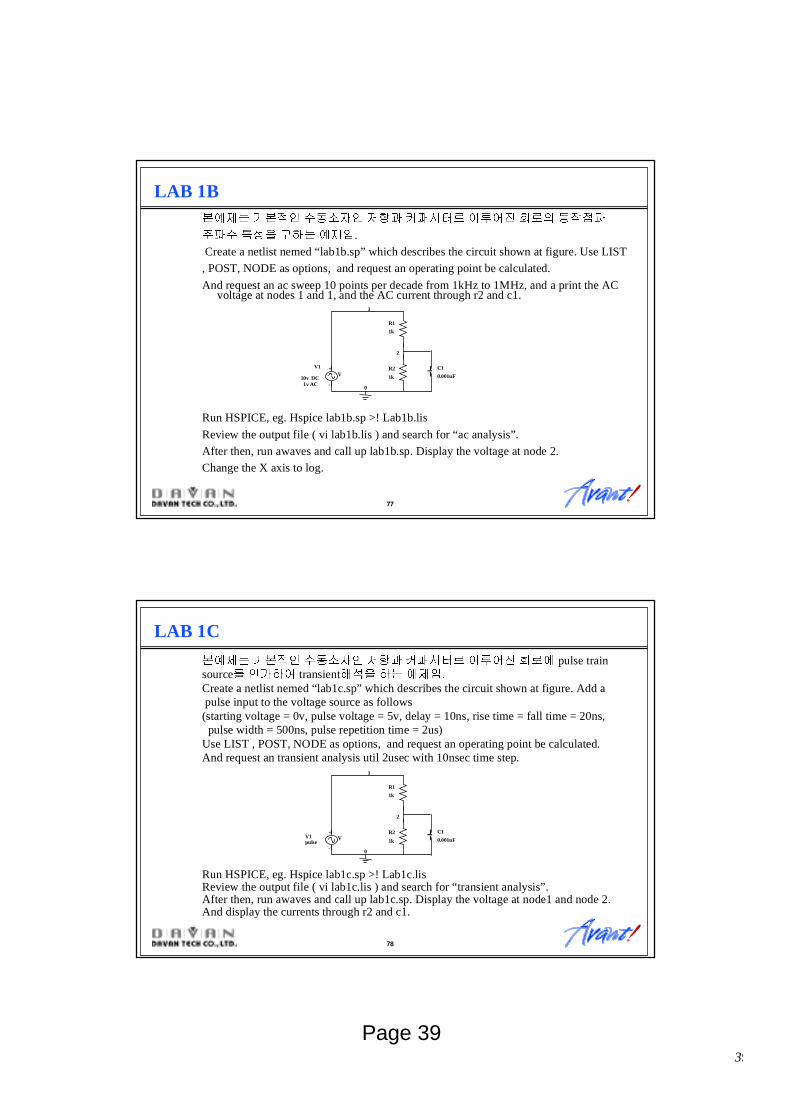
LAB 1C
åõ� �åîe �Æy}e íZé Ñ�É�I aÕ¡± yI½ pulse trainsourcei eíEÙ transienta1 E� õq.Create a netlist nemed “lab1c.sp” which describes the circuit shown at figure. Add a pulse input to the voltage source as follows(starting voltage = 0v, pulse voltage = 5v, delay = 10ns, rise time = fall time = 20ns, pulse width = 500ns, pulse repetition time = 2us)Use LIST , POST, NODE as options, and request an operating point be calculated.And request an transient analysis util 2usec with 10nsec time step.
+
-
VV1pulse
0
1
2
Run HSPICE, eg. Hspice lab1c.sp >! Lab1c.lisReview the output file ( vi lab1c.lis ) and search for “transient analysis”.After then, run awaves and call up lab1c.sp. Display the voltage at node1 and node 2.And display the currents through r2 and c1.
R1
1k
R2
1k
C1
0.001uF

40
Page 40
79
LAB 1D
åõ� �åîe 4� butterworth low-pass filterE éù� ¦�é ÉñîÚ½E ¦�1 í�E� õq.
Create a netlist named “lab1d.sp” which describes the circuit shown at figure.PWL voltage source, 0V at time 0sec, 0V at 1us, 1v at 20us, 0v at 20.1nsAC voltage source, magnitude = 1v phase = 0 degreesAC analysis, 20 points per decade from 100 to 100MegaHzTransient analysis, 2us steps for 40us.View the result of wave form of DB/Phase of voltage at node 3 and transient result ofvoltage at node 3.
+
-
VV1PWL/AC
0
1 2 35
L20.38268U
L11.5772U
C11.5307N
C21.0824N
R11
80
LAB 1E
åõ� �åîe �Æy}e DiodeE device modelE rs í yIE DC ¦�½åE� î�1 DC analysisi ¢EÙ í�E� õqCreate a netlist nemed “lab1e.sp” which describes the circuit shown at figure.Set V1’s voltage to a variable, dv, and sweep dv from 800mV to 1V in 5mV steps.And use following diode model.( .model df d is = 2.6615e-16 rs = 0.0 )Use LIST , POST, NODE as options, put in a print control for v(1) I(d1)
+
-
VV1
0
1
Run HSPICE, eg. Hspice lab1e.sp >! Lab1e.lisReview the output file ( vi lab1e.lis ) and search for “dc transfer”.After then, run awaves and call up lab1c.sp. Display I(d1) with dv as the x-axis. You cansee the unrealistic current spikes due to 0 ohm rs.Change the rs of the diode to 0.01ohms in the model and do the same as above.
D1
df

41
Page 41
81
LAB 1F
åõ� �åîe Peak DetectorE ¦�1 í�E� õq.
Create a netlist named “lab1f.sp” which describes the circuit shown at figure.V1 is a SIN wave source, 0volt offset, 1volt peak amplitude, frequency of 1KHzV2 is a 500mV DC source.Use DN4148 model, print out V(2) and V(1) vs, TIMETransient anlysis, 10us steps for 3ms.Diode model ( .MODEL DN4148 D (CJO=5PF VJ=0.6 M=0.45 RS=0.8 IS=7e-9 + N=2 TT=6e-9 BV=100) )
+
-
VV1SIN
0
1 2
D1DN4148
R11
+
-
V V20.5V
82
LAB 1G
åõ� MOSFETE IV ¦�1 YE� õq.
Create a netlist named “lab1g.sp” which describes the circuit shown at figure.VDS and VGS are DC sources swept by DC analysis.Sweep VDS from 0V to 10V in 500mV increments while sweeping VGS from 0V to 5Vin 1V increments. Print out I(VDS) and I(VGS) vs. VDSUse the MOSFET MOD1 model(.MODEL MOD1 NMOS level = 13 )
+
-
VVGS
0
7
1
+
-
V VDS

42
Page 42
83
LAB 1H
åõ� MOSFET InverterE ¦�1 í�E� õq.
Create a netlist named “lab1h.sp” which describes the circuit shown at figure.The length for both MOS device is 1u, and the width is 20u. The pulse is(vlow=0.2, vhigh=4.8, tdly=2n, tf=fr=1n, pw=5n, trep=20n)The tran is 20n in 200p steps, and use the MOSFET model( .MODEL nch NMOS level = 13 .MODEL pch PMOS level = 13)Sweep VIN from 0V to 5V in 500mV increments. Print out V(out) and V(in).
+
-
VVINPULSE
0
in
+
-
V VDD5V
vdd
out
C10.75pF
Mp1
Mn1
84
Related Documents