ICs for Communications ISDN High Voltage Power Controller IHPC PEB 2026 Version 1.1 Data Sheet 09.99 DS 2

Welcome message from author
This document is posted to help you gain knowledge. Please leave a comment to let me know what you think about it! Share it to your friends and learn new things together.
Transcript

ICs for Communications
ISDN High Voltage Power ControllerIHPC
PEB 2026 Version 1.1
Data Sheet 09.99DS 2

•
For questions on technology, delivery and prices please contact the Infineon Technologies Offices in Germany or the Infineon Technologies Companies and Representatives worldwide: see our webpage at http://www.infineon.com
•
PEB 2026 Revision History: Current Version: 09.99
Previous Version: preliminary Data Sheet 02.96
Page(in previous Version)
Page(in current Version)
Subjects (major changes since last revision)
3-2 Information added about thermal protection and life time
3-3 Information added about parasitic diodes
3-3 Extra paragraphfor subject "IBAT current peak"
16 7-1 Some values for absolute maximum ratings are extended/adapted.
17 7-4 The static thermal resistances are updated. The last two paragraphs on this page, explaning the reason for the different packages are additional.
Edition 09.99Published by Infineon Technologies AG,TR,Balanstraße 73,81541 München© Infineon Technologies AG 1999.All Rights Reserved.Attention please!As far as patents or other rights of third parties are concerned, liability is only assumed for components, not for applications, processes and circuits implemented within components or assemblies.The information describes the type of component and shall not be considered as assured characteristics.Terms of delivery and rights to change design reserved.Due to technical requirements components may contain dangerous substances. For information on the types in question please contact your nearest Infineon Technologies Office.Infineon Technologies AG is an approved CECC manufacturer.PackingPlease use the recycling operators known to you. We can also help you – get in touch with your nearest sales office. By agreement we will take packing material back, if it is sorted. You must bear the costs of transport. For packing material that is returned to us unsorted or which we are not obliged to accept, we shall have to invoice you for any costs incurred.Components used in life-support devices or systems must be expressly authorized for such purpose!Critical components1 of the Infineon Technologies AG, may only be used in life-support devices or systems2 with the express written approval of the Infineon Technologies AG.1 A critical component is a component used in a life-support device or system whose failure can reasonably be
expected to cause the failure of that life-support device or system, or to affect its safety or effectiveness of that device or system.
2 Life support devices or systems are intended (a) to be implanted in the human body, or (b) to support and/or maintain and sustain human life. If they fail, it is reasonable to assume that the health of the user may be en-dangered.
ABM®, AOP®, ARCOFI®, ARCOFI®-BA, ARCOFI®-SP, DigiTape®, EPIC®-1, EPIC®-S, ELIC®, FALC®54, FALC®56, FALC®-E1, FALC®-LH, IDEC®, IOM®, IOM®-1, IOM®-2, IPAT®-2, ISAC®-P, ISAC®-S, ISAC®-S TE, ISAC®-P TE, ITAC®, IWE®, MUSAC®-A, OCTAT®-P, QUAT®-S, SICAT®, SICOFI®, SICOFI®-2, SICOFI®-4, SICOFI®-4µC, SLICOFI® are registered trademarks of Infineon Technologies AG.
ACE™, ASM™, ASP™, POTSWIRE™, QuadFALC™, SCOUT™ are trademarks of Infineon Technologies AG.
PEB 2026PEF 2026
Table of Contents Page
Data Sheet iii 09.99
1 Overview . . . . . . . . . . . . . . . . . . . . . . . . . . . . . . . . . . . . . . . . . . . . . . . . . . 1-11.1 Features . . . . . . . . . . . . . . . . . . . . . . . . . . . . . . . . . . . . . . . . . . . . . . . . . . . 1-1
2 Pin Description . . . . . . . . . . . . . . . . . . . . . . . . . . . . . . . . . . . . . . . . . . . . 2-12.1 Pin Configuration . . . . . . . . . . . . . . . . . . . . . . . . . . . . . . . . . . . . . . . . . . . . 2-12.2 Pin Definitions and Functions . . . . . . . . . . . . . . . . . . . . . . . . . . . . . . . . . . 2-2
3 Functional Description . . . . . . . . . . . . . . . . . . . . . . . . . . . . . . . . . . . . . . 3-1
4 Operating Modes . . . . . . . . . . . . . . . . . . . . . . . . . . . . . . . . . . . . . . . . . . . 4-1
5 Designing the External Components . . . . . . . . . . . . . . . . . . . . . . . . . . . 5-1
6 Application Note . . . . . . . . . . . . . . . . . . . . . . . . . . . . . . . . . . . . . . . . . . . 6-1
7 Electrical Characteristics . . . . . . . . . . . . . . . . . . . . . . . . . . . . . . . . . . . . 7-1
8 Package Outlines . . . . . . . . . . . . . . . . . . . . . . . . . . . . . . . . . . . . . . . . . . . 8-1
PEB 2026PEF 2026
List of Figures Page
Data Sheet iv 09.99
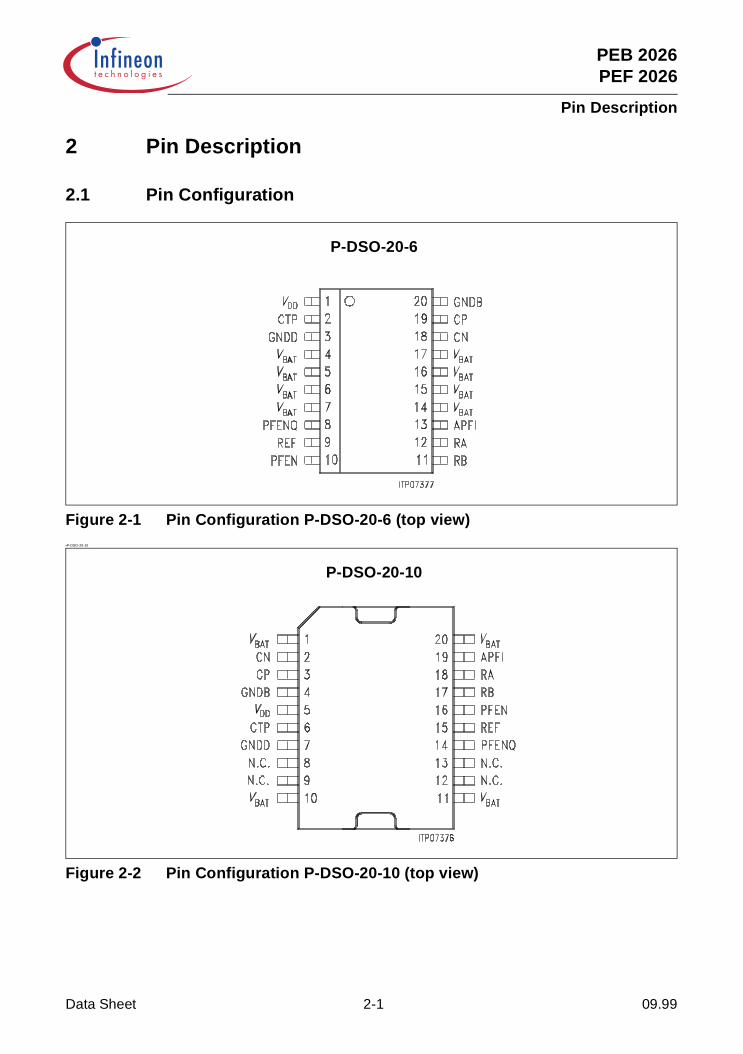
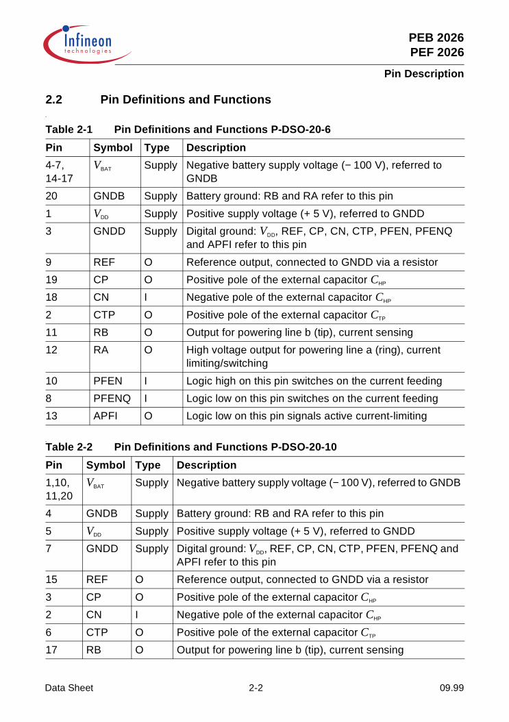
Figure 2-1 Pin Configuration P-DSO-20-6 (top view) . . . . . . . . . . . . . . . . . . . . . . 2-1Figure 2-2 Pin Configuration P-DSO-20-10 (top view) . . . . . . . . . . . . . . . . . . . . . 2-1Figure 3-1 Block Diagram . . . . . . . . . . . . . . . . . . . . . . . . . . . . . . . . . . . . . . . . . . . 3-1Figure 5-1 Current limit ILimit,ON as a function of RREF (typical values) . . . . . . . . . . 5-1Figure 5-2 Power Supply Current IBAT as a function of RREF (typical values) . . . . 5-2Figure 5-3 Power Supply Current IDD as a function of RREF (typical values) . . . . 5-2Figure 5-4 Corner frequency of high-pass filter as a function of CHP
(typical values) . . . . . . . . . . . . . . . . . . . . . . . . . . . . . . . . . . . . . . . . . . . 5-3Figure 5-5 Time constant of high-pass filter as a function of CHP
(typical values) . . . . . . . . . . . . . . . . . . . . . . . . . . . . . . . . . . . . . . . . . . . 5-3Figure 5-6 Delay time of the low-pass filter for the status output signal
(typical values) . . . . . . . . . . . . . . . . . . . . . . . . . . . . . . . . . . . . . . . . . . . 5-4Figure 5-7 Delay time of the low-pass filter for the status output signal
(typical values) . . . . . . . . . . . . . . . . . . . . . . . . . . . . . . . . . . . . . . . . . . . 5-4Figure 6-1 Application Circuit . . . . . . . . . . . . . . . . . . . . . . . . . . . . . . . . . . . . . . . . 6-1Figure 7-1 Power Dissipation and Reference Voltage Output. . . . . . . . . . . . . . . . 7-6Figure 7-2 Maximal Line Currents . . . . . . . . . . . . . . . . . . . . . . . . . . . . . . . . . . . . . 7-7Figure 7-3 Resistances . . . . . . . . . . . . . . . . . . . . . . . . . . . . . . . . . . . . . . . . . . . . . 7-7Figure 7-4 Line Status . . . . . . . . . . . . . . . . . . . . . . . . . . . . . . . . . . . . . . . . . . . . . . 7-8Figure 7-5 Line Status under Superimposed Longitudinal Current . . . . . . . . . . . . 7-8Figure 7-6 Timing-Characteristics . . . . . . . . . . . . . . . . . . . . . . . . . . . . . . . . . . . . . 7-9Figure 7-7 Lightning Voltage Influence . . . . . . . . . . . . . . . . . . . . . . . . . . . . . . . . 7-10

PEB 2026PEF 2026
List of Tables Page
Data Sheet v 09.99
Table 2-1 Pin Definitions and Functions P-DSO-20-6 . . . . . . . . . . . . . . . . . . . . 2-2Table 2-2 Pin Definitions and Functions P-DSO-20-10 . . . . . . . . . . . . . . . . . . . 2-2Table 7-1 Absolute Maximum Ratings . . . . . . . . . . . . . . . . . . . . . . . . . . . . . . . . 7-1Table 7-2 Operating Range . . . . . . . . . . . . . . . . . . . . . . . . . . . . . . . . . . . . . . . . 7-2Table 7-3 Power-Supply. . . . . . . . . . . . . . . . . . . . . . . . . . . . . . . . . . . . . . . . . . . 7-3Table 7-4 DC-Characteristics . . . . . . . . . . . . . . . . . . . . . . . . . . . . . . . . . . . . . . . 7-3Table 7-5 Indication of Current Limit . . . . . . . . . . . . . . . . . . . . . . . . . . . . . . . . . 7-4Table 7-6 Timing-Characteristics . . . . . . . . . . . . . . . . . . . . . . . . . . . . . . . . . . . . 7-6
PEB 2026PEF 2026
Overview
1 OverviewThe IHPC is an integrated power controller especially designed for feeding two-wireISDN-transmission lines. One line can be powered by one IHPC. An external resistordefines the value of the current-limit for the line. Powering can be switched on or off bythe logic inputs “PFEN” and “PFENQ”. With a logic low at the “APFI” output the IHPCsignals that current-limiting is active; this signal is low-pass filtered. An external capacitordefines the corner frequency of this low-pass filter and the resulting delay timerespectively. A second external capacitor is needed to make sure that longitudinaldisturbances (AC) will not produce a current limiting effect. Line current-limiting andreducing this limiting level in case of overtemperature guards the IHPC againstoverloads.
Data Sheet 1-1 09.99
ISDN High Voltage Power ControllerIHPC
PEB 2026
Version 1.1 CMOS
P-DSO-20-6
P-DSO-20-10
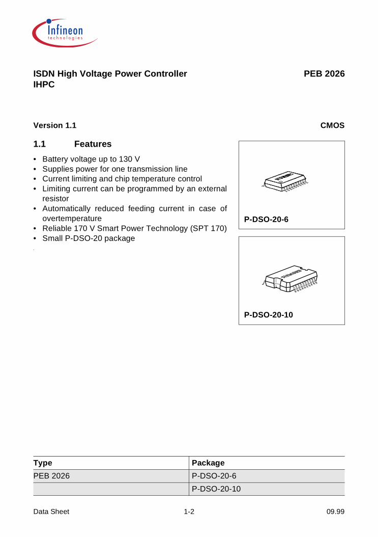
1.1 Features
• Battery voltage up to 130 V• Supplies power for one transmission line• Current limiting and chip temperature control• Limiting current can be programmed by an external
resistor• Automatically reduced feeding current in case of
overtemperature• Reliable 170 V Smart Power Technology (SPT 170)• Small P-DSO-20 package•
Data Sheet 1-2 09.99
Type Package
PEB 2026 P-DSO-20-6
P-DSO-20-10
PEB 2026PEF 2026
Pin Description
2 Pin Description
2.1 Pin Configuration
Figure 2-1 Pin Configuration P-DSO-20-6 (top view)•P-DSO-20-10
Figure 2-2 Pin Configuration P-DSO-20-10 (top view)
P-DSO-20-6
P-DSO-20-10
Data Sheet 2-1 09.99
PEB 2026PEF 2026
Pin Description
2.2 Pin Definitions and Functions •
•
Table 2-1 Pin Definitions and Functions P-DSO-20-6
Pin Symbol Type Description
4-7,14-17
VBAT Supply Negative battery supply voltage (− 100 V), referred to GNDB
20 GNDB Supply Battery ground: RB and RA refer to this pin
1 VDD Supply Positive supply voltage (+ 5 V), referred to GNDD
3 GNDD Supply Digital ground: VDD, REF, CP, CN, CTP, PFEN, PFENQ and APFI refer to this pin
9 REF O Reference output, connected to GNDD via a resistor
19 CP O Positive pole of the external capacitor CHP
18 CN I Negative pole of the external capacitor CHP
2 CTP O Positive pole of the external capacitor CTP
11 RB O Output for powering line b (tip), current sensing
12 RA O High voltage output for powering line a (ring), current limiting/switching
10 PFEN I Logic high on this pin switches on the current feeding
8 PFENQ I Logic low on this pin switches on the current feeding
13 APFI O Logic low on this pin signals active current-limiting
Table 2-2 Pin Definitions and Functions P-DSO-20-10
Pin Symbol Type Description
1,10,11,20
VBAT Supply Negative battery supply voltage (− 100 V), referred to GNDB
4 GNDB Supply Battery ground: RB and RA refer to this pin
5 VDD Supply Positive supply voltage (+ 5 V), referred to GNDD
7 GNDD Supply Digital ground: VDD, REF, CP, CN, CTP, PFEN, PFENQ and APFI refer to this pin
15 REF O Reference output, connected to GNDD via a resistor
3 CP O Positive pole of the external capacitor CHP
2 CN I Negative pole of the external capacitor CHP
6 CTP O Positive pole of the external capacitor CTP
17 RB O Output for powering line b (tip), current sensing
Data Sheet 2-2 09.99
PEB 2026PEF 2026
Pin Description
•
18 RA O High voltage output for powering line a (ring), current limiting/switching
16 PFEN I Logic high on this pin switches on the current feeding
14 PFENQ I Logic low on this pin switches on the current feeding
19 APFI O Logic low on this pin signals active current-limiting
Table 2-2 Pin Definitions and Functions P-DSO-20-10 (cont’d)
Pin Symbol Type Description
Data Sheet 2-3 09.99

PEB 2026PEF 2026
Functional Description
3 Functional Description•
Figure 3-1 Block Diagram
The current flowing from GNDB to RB is measured. A down scaled image of this currentis filtered by a high-pass filter with a corner frequency fCHP of approximately 3 Hz (see
Data Sheet 3-1 09.99

PEB 2026PEF 2026
Functional Description
Figure 5-4). This filter needs the external capacitor CHP. This “AC”-current is subtractedfrom the reference-current generated in the bandgap. The value of the reference-currentis defined by the external resistor RREF.
In case of overtemperature the thermal protection TH-PROT sinks a current, so that thecurrent ILimit is reduced. So in case of high power dissipation on chip the junctiontemperature is limited to about 165 °C.
This function is a protection against instant damages due to overload at the outputs.Continuous high temperatures during operation, however, will reduce the life time of theIHPC. A maximum junction temperature of 150°C shall not be exceeded (See section 7,"Electrical Characteristics")
Measures have to be taken to switch off the IHPC in case of a short-circuit. E.g. if pinAPFI indicates active current-limiting, the IHPC should be deactivated after 1.5 sec usingpin PFEN or PFENQ. A consecutive power-up attempt shall give enough time to theIHPC to cool down again (e.g. 30 sec).
The current ILimit is reflected to the output current ILine flowing from RA to VBAT using theoperational-amplifier OP, the transistor TL and two resistors (4 Ω, 4 kΩ).
ILine,max (t) = 1000 × ILimit (t) = 1000 × (IREF − ITH-PROT (t) − IAC (t))
In case of “no current-limiting” the output voltage of the operational-amplifier OP is equalto the positive OP-supply voltage. The transistor TL is “switched on”.
If the output current ILine rises to ILine,max the current-mirror becomes active and keeps theoutput current at this level.
The voltage level at the gate of transistor TL shows the state of the current-limiter(current-limiting active or not). This state-signal is filtered by a low-pass filter andgenerates the logic output APFI. The external capacitor CTP of this low-pass filter definesthe corner frequency and the resulting delay times tLIMON (Spec.-No.: 17) and tLIMOFF (Spec.-No.: 18) respectively.
Summarized, the current sensor I-SENS and the high-pass filter prevent, that alongitudinal disturbance in the frequency range from about (5*fCHP) to about 100kHzresult in a current limitation. This applies if the maximum amplitude of the longitudinalcurrent is lower than about half of the current limit (Spec.-No.: 3) defined by the externalresistor RREF, see also Spec.-No.: 15 and 16.There is also another effect from the current sensing and high-pass filtering, which canbe seen when changing from status LIMOFF to LIMON. This can occur by switchingpower on to the line (loading the line capacitor) or in case of short-circuiting the line. Theresulting current transient starts at half of ILine,max and increases (capacitor loadingfunction) to ILine,max with a time constant tCHP also defined by the value of CHP.
Data Sheet 3-2 09.99
PEB 2026PEF 2026
Functional Description
The diodes connected to GNDB and RB protect the IHPC against lightning andovervoltages (see Absolute Maximum Ratings). The diode Dp is the parasitic bulk-drain-diode of the DMOS-transistor TL.
Because of technology reasons („p“-substrate, junction isolation) there are also parasiticdiodes from pin VBAT to all other pins.
IBAT current peak:
When line feeding is switched on (transistor TL is on) and a short circuit occurs betweenpins RA and GNDB (or GNDD) then it needs a certain time to unload the gate-source-capacitance of TL and to limit the current to the defined maximum value. In the meantimea current peak IBAT on the supply voltage VBAT can be seen.
An overvoltage protection circuit for pin RA, for example can produce such a short circuitbetween pins RA and GNDB.
In the IHPC a fast bipolar npn-transistor limits such current peaks. With VBAT =100 V, theresulting IBAT current transient has the profile of one triangular pulse with a peak value ofabout 1.5A and a time duration (50% to 50%) of about 130nsec. •
Data Sheet 3-3 09.99
PEB 2026PEF 2026
Operating Modes
Data Sheet 4-1 09.99
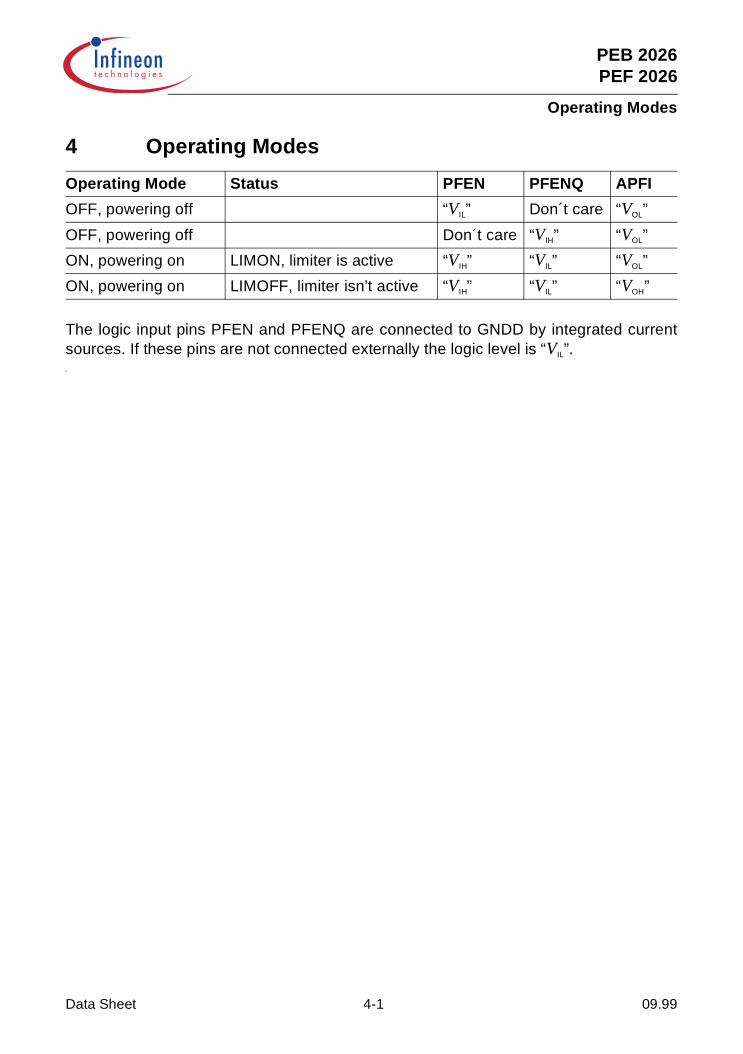
4 Operating Modes
The logic input pins PFEN and PFENQ are connected to GNDD by integrated currentsources. If these pins are not connected externally the logic level is “VIL”.•
Operating Mode Status PFEN PFENQ APFI
OFF, powering off “VIL” Don´t care “VOL”
OFF, powering off Don´t care “VIH” “VOL”
ON, powering on LIMON, limiter is active “VIH” “VIL” “VOL”
ON, powering on LIMOFF, limiter isn’t active “VIH” “VIL” “VOH”
PEB 2026PEF 2026
Designing the External Components
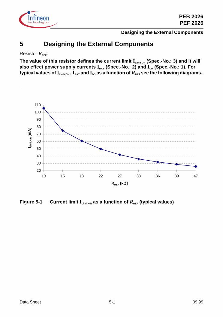
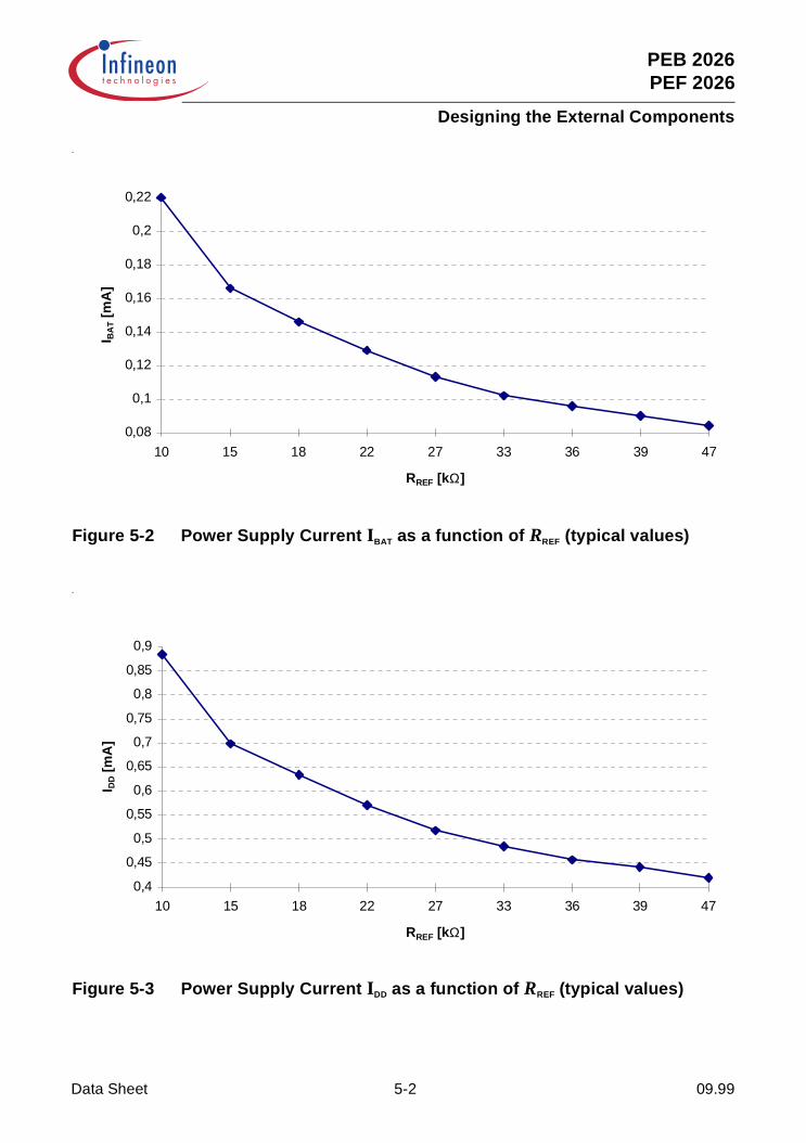
5 Designing the External ComponentsResistor RREF:
The value of this resistor defines the current limit ILimit,ON (Spec.-No.: 3) and it will also effect power supply currents IBAT (Spec.-No.: 2) and IDD (Spec.-No.: 1). For typical values of ILimit,ON , IBAT and IDD as a function of RREF see the following diagrams.
•
Figure 5-1 Current limit ILimit,ON as a function of RREF (typical values)
20
30
40
50
60
70
80
90
100
110
10 15 18 22 27 33 36 39 47
RREF [kΩ]
I Lim
it,O
N [
mA
]
Data Sheet 5-1 09.99
PEB 2026PEF 2026
Designing the External Components
•
Figure 5-2 Power Supply Current IBAT as a function of RREF (typical values)
•
Figure 5-3 Power Supply Current IDD as a function of RREF (typical values)
0,08
0,1
0,12
0,14
0,16
0,18
0,2
0,22
10 15 18 22 27 33 36 39 47
RREF [kΩ]
I BA
T [
mA
]
0,4
0,45
0,5
0,55
0,6
0,65
0,7
0,75
0,8
0,85
0,9
10 15 18 22 27 33 36 39 47
RREF [kΩ]
I DD [
mA
]
Data Sheet 5-2 09.99

PEB 2026PEF 2026
Designing the External Components
Capacitor CHP:
The value of this capacitor defines the corner frequency fCHP of the high-pass filter andthe time constant tCHP of the current transient described at the last but one paragraph ofchapter 2. The following diagrams show typical values of fCHP and tCHP as a function of CHP.•
Figure 5-4 Corner frequency of high-pass filter as a function of CHP (typical values)
•
Figure 5-5 Time constant of high-pass filter as a function of CHP (typical values)
05
1015202530354045
0,33 0,47 0,68 1 2,2 3,3 4,7 6,8
CHP [µF]
f CH
P [
Hz]
020406080
100120140160180
0,33 0,47 0,68 1 2,2 3,3 4,7 6,8
CHP [µF]
t CH
P [
mse
c]
Data Sheet 5-3 09.99
PEB 2026PEF 2026
Designing the External Components
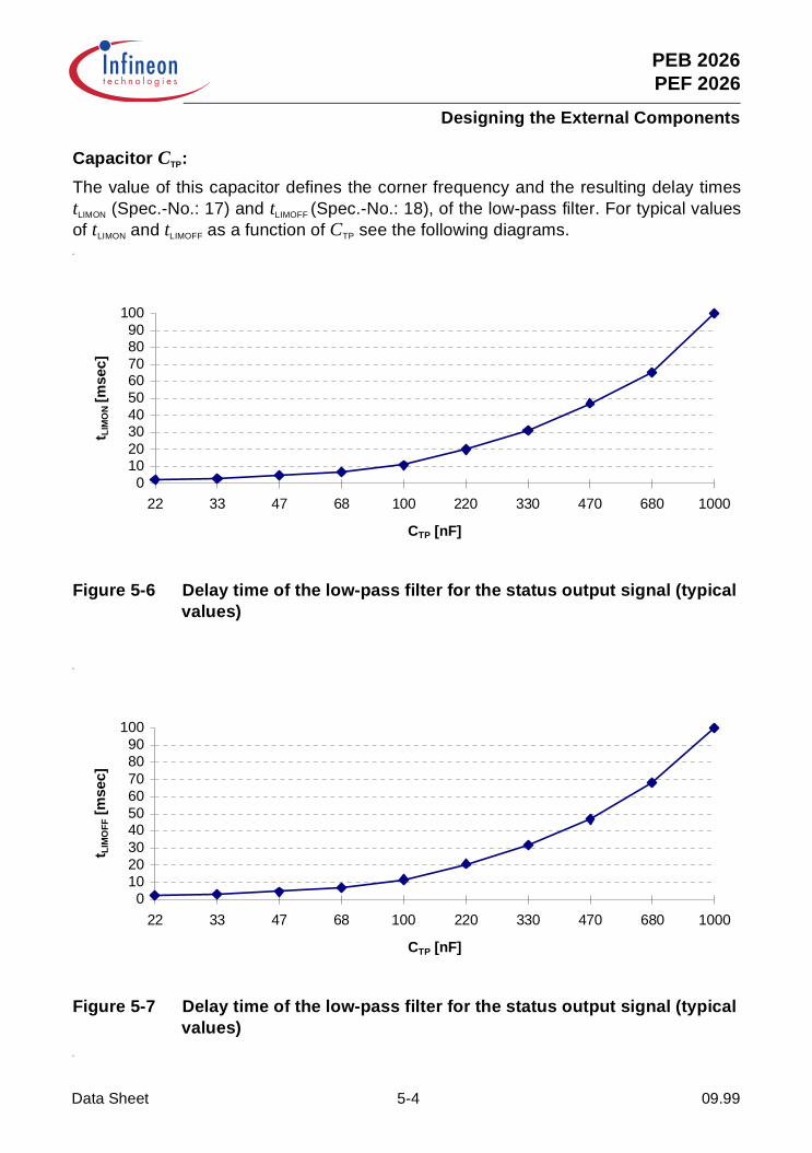
Capacitor CTP:
The value of this capacitor defines the corner frequency and the resulting delay timestLIMON (Spec.-No.: 17) and tLIMOFF (Spec.-No.: 18), of the low-pass filter. For typical valuesof tLIMON and tLIMOFF as a function of CTP see the following diagrams.•
Figure 5-6 Delay time of the low-pass filter for the status output signal (typical values)
•
Figure 5-7 Delay time of the low-pass filter for the status output signal (typical values)
•
0102030405060708090
100
22 33 47 68 100 220 330 470 680 1000
CTP [nF]
t LIM
ON [
mse
c]
0102030405060708090
100
22 33 47 68 100 220 330 470 680 1000
CTP [nF]
t LIM
OF
F [m
sec]
Data Sheet 5-4 09.99
PEB 2026PEF 2026
Application Note
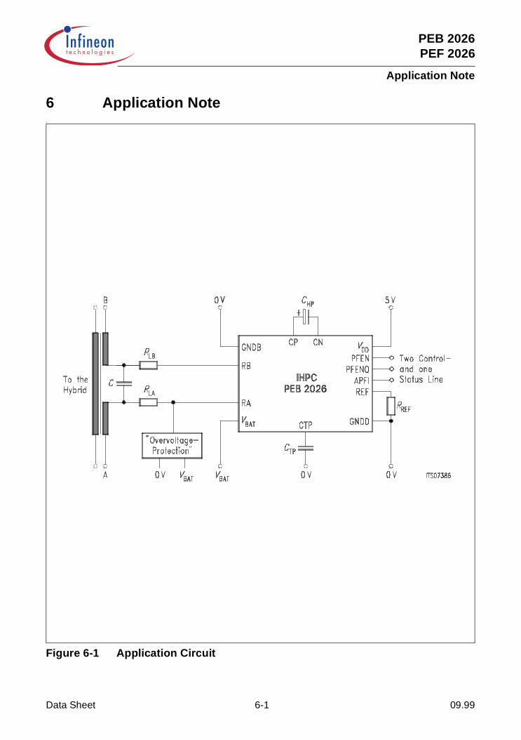
6 Application Note•
Figure 6-1 Application Circuit
Data Sheet 6-1 09.99

PEB 2026PEF 2026
Application Note
RREF Defines the current-limit and the internal biasing currents. Asmaller/bigger value increases/decreases the current limit. Itwill also effect power supply currents.
CTP Defines with an internal resistor the delay time (a typical valueis 20 msec) from the low pass filter, whose output signal iscalled ‘APFI’. Short disturbances will therefore be filtered. Asmaller/bigger value decreases/increases the delay time.
CHP Defines with an internal resistor the corner frequency from ahigh pass filter. It is used to make sure that longitudinaldisturbances (AC) will not produce a current limiting effect. Asmaller/bigger value decreases/increases the cornerfrequency.
RLA, RLB These resistors limit the peak currents during lightningtransients. The maximum value for these resistors is definedby the allowed voltage drop on the resistors.
C The AC-signal-current will be shunted by this capacitor.
A, B A- and B-line to the subscriber
VBAT The most negative supply voltage; also called battery voltage.
overvoltage protection This circuit makes sure that the voltage from RA to VBAT will notexceed the defined limits in case of lightning (see AbsoluteMaximum Ratings).
Recommended Device Values:
RREF 22 kΩ,Current limiting is set to 50 mA
CTP 220 nF,‘APFI’ delay time is set to 20 msec
CHP 4.7 µF,AC longitudinal disturbances in a frequency rangehigher than 16.666 Hz do not effect a current limiting.
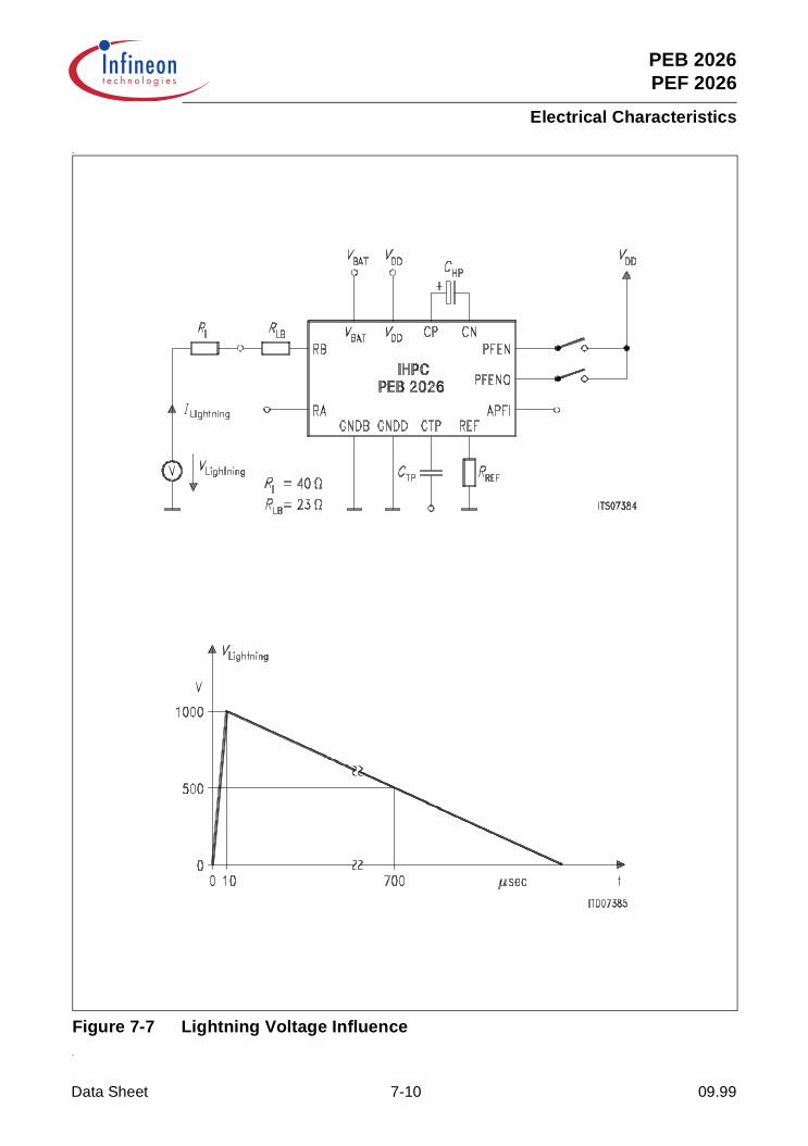
RLA, RLB 23 Ω,Minimum value, so that peek currents don’t exceed 16 A(using voltage peek = 1 kV from 40 Ω source resistance) incase of lightning.
•
Data Sheet 6-2 09.99
PEB 2026PEF 2026
Electrical Characteristics
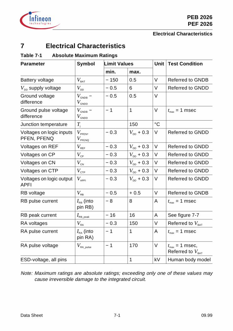
7 Electrical Characteristics
Note: Maximum ratings are absolute ratings; exceeding only one of these values maycause irreversible damage to the integrated circuit.
Table 7-1 Absolute Maximum Ratings
Parameter Symbol Limit Values Unit Test Condition
min. max.
Battery voltage VBAT − 150 0.5 V Referred to GNDB
VDD supply voltage VDD − 0.5 6 V Referred to GNDD
Ground voltage difference
VGNDB −VGNDD
− 0.5 0.5 V
Ground pulse voltage difference
VGNDB −VGNDD
− 1 1 V tmax = 1 msec
Junction temperature Tj 150 °C
Voltages on logic inputs PFEN, PFENQ
VPFEN,VPFENQ
− 0.3 VDD + 0.3 V Referred to GNDD
Voltages on REF VREF − 0.3 VDD + 0.3 V Referred to GNDD
Voltages on CP VCP − 0.3 VDD + 0.3 V Referred to GNDD
Voltages on CN VCN − 0.3 VDD + 0.3 V Referred to GNDD
Voltages on CTP VCTP − 0.3 VDD + 0.3 V Referred to GNDD
Voltages on logic output APFI
VAPFI − 0.3 VDD + 0.3 V Referred to GNDD
RB voltage VRB − 0.5 + 0.5 V Referred to GNDB
RB pulse current IRB (intopin RB)
− 8 8 A tmax = 1 msec
RB peak current IRB_peak − 16 16 A See figure 7-7
RA voltages VRA − 0.3 150 V Referred to VBAT
RA pulse current IRA (intopin RA)
− 1 1 A tmax = 1 msec
RA pulse voltage VRA_pulse − 1 170 V tmax = 1 msec, Referred to VBAT
ESD-voltage, all pins 1 kV Human body model
Data Sheet 7-1 09.99
PEB 2026PEF 2026
Electrical Characteristics
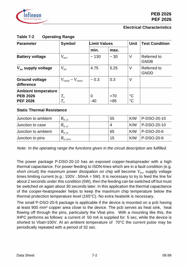
Note: In the operating range the functions given in the circuit description are fulfilled.
The power package P-DSO-20-10 has an exposed copper-heatspreader with a highthermal capacitance. For power feeding to ISDN-lines which are in a fault condition (e.g.short circuit) the maximum power dissipation on chip will become VBAT supply voltagetimes limiting current (e.g.: 100V * 50mA = 5W). It is necessary to try to feed the line forabout 2 seconds under this condition (5W), then the feeding can be switched off but mustbe switched on again about 30 seconds later. In this application the thermal capacitanceof the cooper-heatspreader helps to keep the maximum chip temperature below thethermal protection temperature level (165°C). No extra heatsink is necessary.
The small P-DSO-20-6 package is applicable if the device is mounted on a pcb havingat least 900 mm² copper area close to the device. The pcb serves as heat sink, heatflowing off through the pins, particularly the Vbat pins. With a mounting like this, theIHPC performs as follows: a current of 50 mA is supplied for 5 sec, while the device isshorted to Vbat=100V. At an ambient temperature of 70°C the current pulse may beperiodically repeated with a period of 32 sec.
Table 7-2 Operating Range
Parameter Symbol Limit Values Unit Test Condition
min. max.
Battery voltage VBAT − 130 − 30 V Referred to GNDB
VDD supply voltage VDD 4.75 5.25 V Referred to GNDD
Ground voltage difference
VGNDB − VGNDD − 0.3 0.3 V
Ambient temperaturePEB 2026PEF 2026
TA
TA
0-40
+70+85
°C°C
Static Thermal Resistance
Junction to ambient Rth, jA 55 K/W P-DSO-20-10
Junction to case Rth, jC 4 K/W P-DSO-20-10
Junction to ambient Rth, jA 65 K/W P-DSO-20-6
Junction to pins Rth, jPins 15 K/W P-DSO-20-6
Data Sheet 7-2 09.99

PEB 2026PEF 2026
Electrical Characteristics
Electrical Parameters
Typical values are defined at the following test conditions:
VDD=5V± 1 %CHP=4.7µF± 10 %(6.3 V)
VBAT=− 100V± 1 %CTP=220nF± 10 %(6.3 V)
RLA=23Ω± 1 %TA=25± 5 °CRLB=23Ω± 1 %RLine=± 0.1 %
RREF=22kΩ± 1 %no heatsink
Min. and max. values are in force within the whole operating range.
Table 7-3 Power-Supply
No. Parameter Symbol Limit Values Unit Test Condition
TestFig.
Mode
min. typ. max.
Supply Currents (IRB = IRA = 0)
1 VDD current IDD 0.57 0.9 mA 7-1 all
2 VBAT current IBAT 0.13 0.25 mA 7-1 all
Table 7-4 DC-Characteristics
No. Parameter Symbol Limit Values Unit Test Condition
TestFig.
Mode
min. typ. max.
Maximal Line Currents
3 Line current Ilimit,ON 45 50 55 mA 7-2 ON, Sta-tus: LIMON
4 Line current Imax,OFF 0 10 µA 7-2 OFF
Logic Input Levels on PFEN and PFENQ
5 H-input voltage VIH 2 V all
6 L-input voltage VIL 0.8 V all
7 Input current Iinp 2 11 20 µA 0.8 V < = Vinp < = VDD
all
Data Sheet 7-3 09.99
PEB 2026PEF 2026
Electrical Characteristics
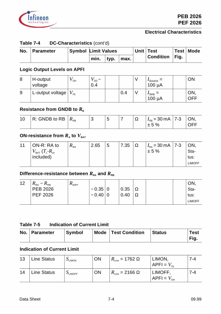
•
Logic Output Levels on APFI
8 H-output voltage
VOH VDD − 0.4
V ISource =100 µA
ON
9 L-output voltage VOL 0.4 V ISink =100 µA
ON, OFF
Resistance from GNDB to RB
10 R: GNDB to RB RRB 3 5 7 Ω IRB = 30 mA ± 5 %
7-3 ON, OFF
ON-resistance from RA to VBAT
11 ON-R: RA to VBAT (TL-Ron included)
RRA 2.65 5 7.35 Ω IRA = 30 mA ± 5 %
7-3 ON, Sta-tus: LIMOFF
Difference-resistance between RRA and RRB
12 RRA − RRB PEB 2026PEF 2026
RDIFF
− 0.35− 0.40
00
0.350.40
ΩΩ
ON, Sta-tus: LIMOFF
Table 7-5 Indication of Current Limit
No. Parameter Symbol Mode Test Condition Status TestFig.
Indication of Current Limit
13 Line Status SLIMON ON RLine = 1762 Ω LIMON,APFI = VOL
7-4
14 Line Status SLIMOFF ON RLine = 2166 Ω LIMOFF,APFI = VOH
7-4
Table 7-4 DC-Characteristics (cont’d)
No. Parameter Symbol Limit Values Unit Test Condition
TestFig.
Mode
min. typ. max.
Data Sheet 7-4 09.99
PEB 2026PEF 2026
Electrical Characteristics
Calculation and Values of RLine
RLine = – RRA – RRB – RLA – RLB = – 5 Ω – 5 Ω – 23 Ω – 23 Ω
where:
RLA, RLB ... referred to page 7-3, electrical parameters
RRA, RRB ... referred to Spec.-No.: 10 and 11
Note: In some of these cases the IHPC will limit the line current to lower values.
Indication of Current Limit under Superimposed Longitudinal Current
15 Line Status SLLIMON ON RLine = 1482 Ω LIMON,APFI = VOL
7-5
16 Line Status SLLIMOFF ON RLine = 2801 Ω LIMOFF,APFI = VOH
7-5
ILine RLine
35 mA 2801 Ω
45 mA 2166 Ω
55 mA 1762 Ω
65 mA 1482 Ω
Table 7-5 Indication of Current Limit (cont’d)
No. Parameter Symbol Mode Test Condition Status TestFig.
VBAT
ILine--------------
100VILine--------------
Data Sheet 7-5 09.99
PEB 2026PEF 2026
Electrical Characteristics
•.
•
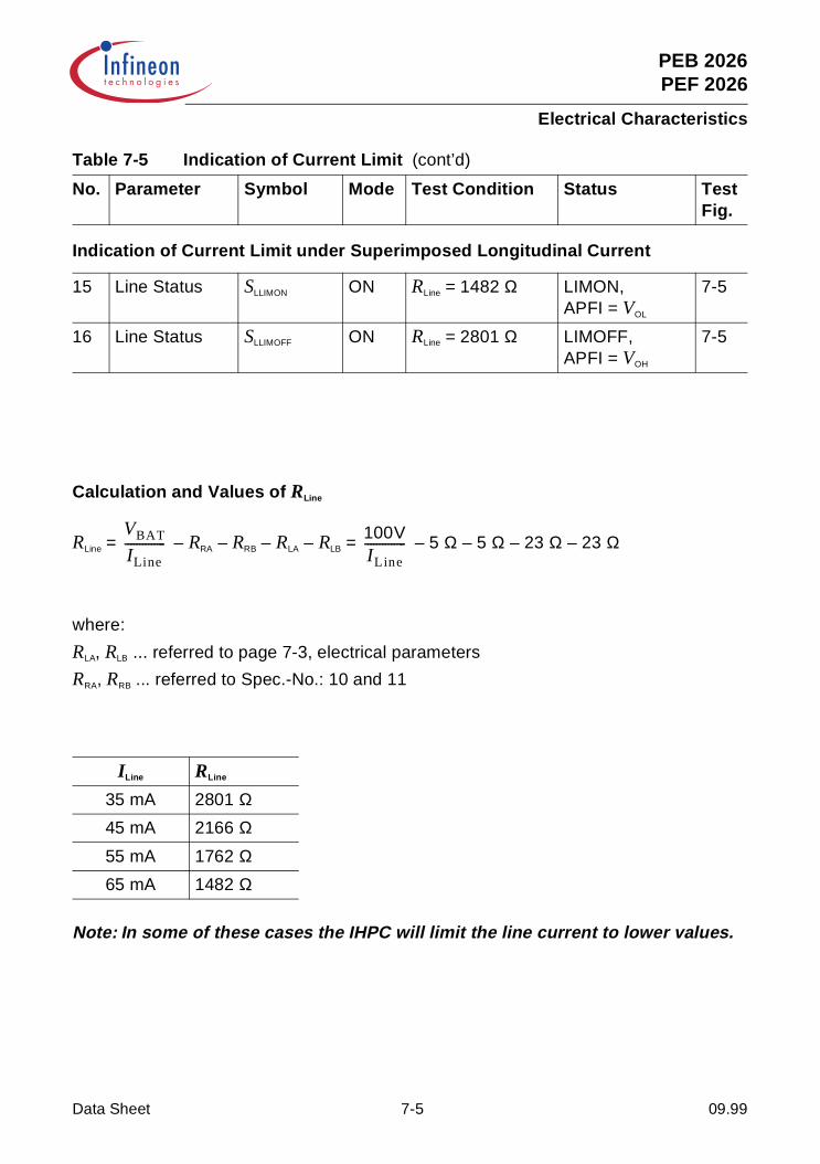
Figure 7-1 Power Dissipation and Reference Voltage Output
Table 7-6 Timing-Characteristics
No.
Parameter
Symbol Limit Values Unit Test Condition TestFig.
Modemin
.typ. max
.
Delay from Begin/End of Current Limiting to Status LIMON/LIMOFF
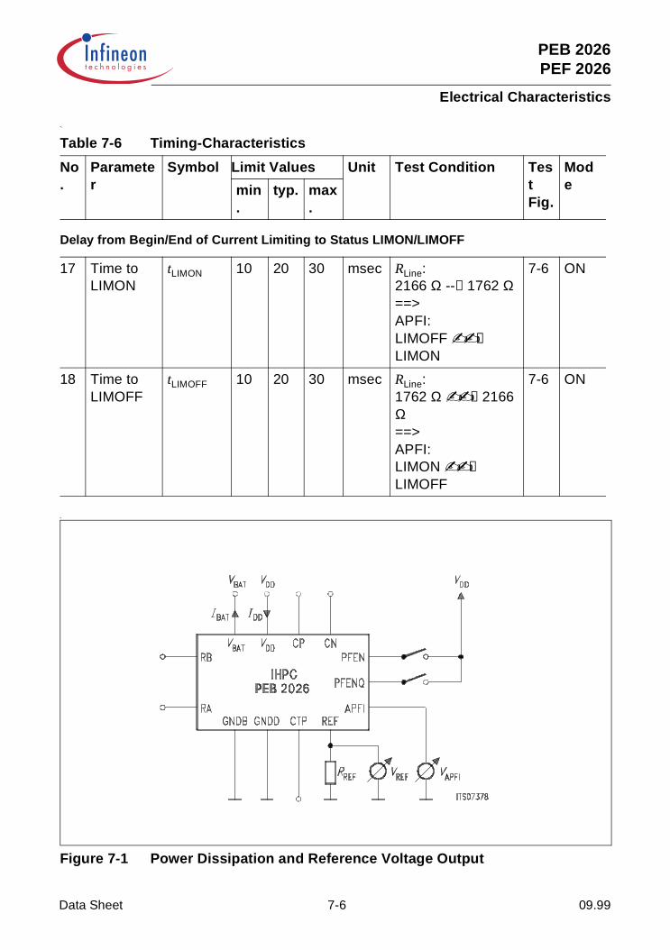
17 Time to LIMON
tLIMON 10 20 30 msec RLine:2166 Ω -- 1762 Ω==>APFI: LIMOFF
LIMON
7-6 ON
18 Time to LIMOFF
tLIMOFF 10 20 30 msec RLine:1762 Ω 2166 Ω==>APFI: LIMON
LIMOFF
7-6 ON
Data Sheet 7-6 09.99

PEB 2026PEF 2026
Electrical Characteristics
•
Figure 7-2 Maximal Line Currents•
Figure 7-3 Resistances
Data Sheet 7-7 09.99

PEB 2026PEF 2026
Electrical Characteristics
•
Figure 7-4 Line Status•
Figure 7-5 Line Status under Superimposed Longitudinal Current
Data Sheet 7-8 09.99
PEB 2026PEF 2026
Electrical Characteristics
•
Figure 7-6 Timing-Characteristics
Data Sheet 7-9 09.99
PEB 2026PEF 2026
Electrical Characteristics
•
Figure 7-7 Lightning Voltage Influence•
Data Sheet 7-10 09.99
PEB 2026PEF 2026
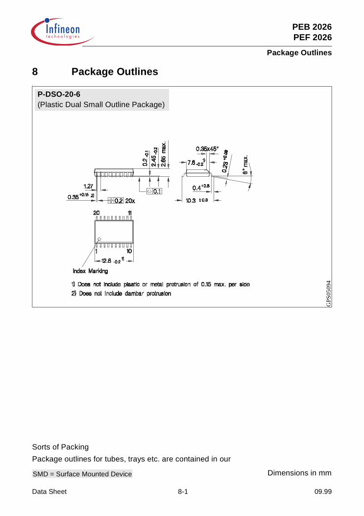
Package Outlines
8 Package Outlines•
P-DSO-20-6(Plastic Dual Small Outline Package)
GPS
0509
4
Sorts of Packing
Package outlines for tubes, trays etc. are contained in our
Dimensions in mmSMD = Surface Mounted Device
Data Sheet 8-1 09.99
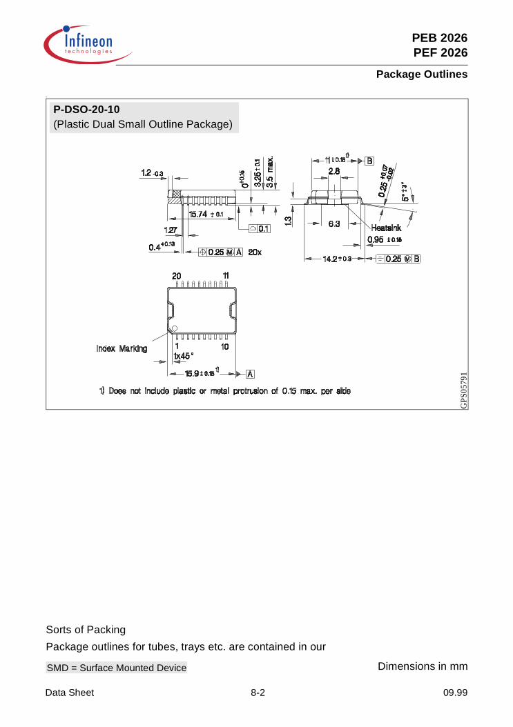
PEB 2026PEF 2026
Package Outlines
•
P-DSO-20-10(Plastic Dual Small Outline Package)
GP
S057
91
Sorts of Packing
Package outlines for tubes, trays etc. are contained in our
Dimensions in mmSMD = Surface Mounted Device
Data Sheet 8-2 09.99
Related Documents