IC Manufacturing Process Group 6

Welcome message from author
This document is posted to help you gain knowledge. Please leave a comment to let me know what you think about it! Share it to your friends and learn new things together.
Transcript

ICManufacturingProcessGroup 6
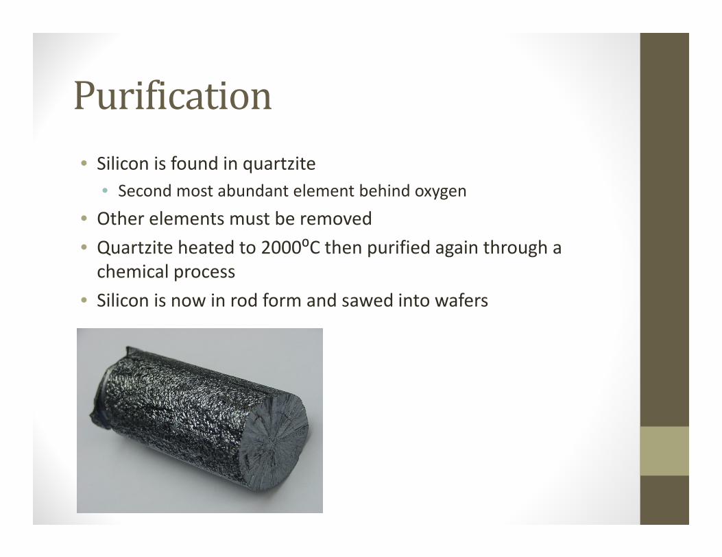
Purification• Silicon is found in quartzite
• Second most abundant element behind oxygen• Other elements must be removed• Quartzite heated to 2000⁰C then purified again through a chemical process
• Silicon is now in rod form and sawed into wafers

WaferPreparation• Wafer is polished to be almost mirror like• Final chemical process removes polishing materials• Wafers packaged in ultra‐clean facility and ready for the fabrication process

SemiconductorFabricationPlant• Built to keep dust particles off of semiconductors, to dampen vibrations, and to control humidity and temperature
• Cost to build is at least $1 billion• Equipment can cost anywhere from $700,000 to $4,000,000
• Hundreds of pieces of equipment are needed
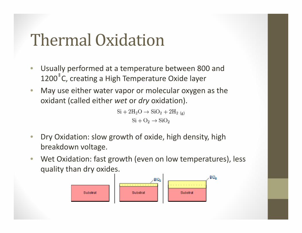
ThermalOxidation• Usually performed at a temperature between 800 and
1200 ̊̊C, crea ng a High Temperature Oxide layer• May use either water vapor or molecular oxygen as the
oxidant (called either wet or dry oxidation).
• Dry Oxidation: slow growth of oxide, high density, high breakdown voltage.
• Wet Oxidation: fast growth (even on low temperatures), less quality than dry oxides.

Photomasking
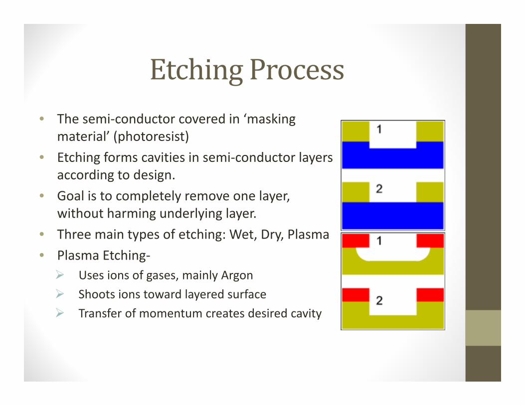
EtchingProcess• The semi‐conductor covered in ‘masking
material’ (photoresist)• Etching forms cavities in semi‐conductor layers
according to design.• Goal is to completely remove one layer,
without harming underlying layer.• Three main types of etching: Wet, Dry, Plasma • Plasma Etching‐ Uses ions of gases, mainly Argon Shoots ions toward layered surface Transfer of momentum creates desired cavity

DiffusionProcess• Pure silicon doped with specific types of atoms
Alters electrical properties, mainly conductivity Allows one to determine the carrier concentration
• Atoms used for doping: Group III (boron)‐ produce p‐type semiconductor Group V (phosphorous)‐ produce n‐type
semiconductor
• Heated to extreme temperatures to ‘diffuse’ with intrinsic silicon

IonImplantation• Process of shooting ions of the desired dopant species into the
wafer through openings in the oxide or photoresist.• Low temperature technique.• Provides flexibility not available with diffusion.• Ion Implanter is a large complex and expensive piece of
equipment. It’s made of several vacuum systems and a computer controlled electronic system.
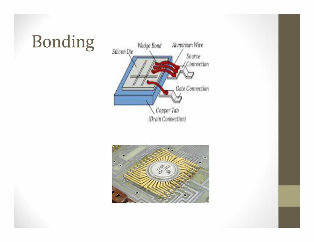
Metallization,Bonding,andPackaging• Metallization is a specialized deposition process that forms critical interconnections between different areas of the chip and different transistors.
• Also used to form the bonding pads that connect the chip to package and then to the circuit board of the system it supports.
• Wire Bonding is used to connect the bonding pads on the die to the post (bonding area). There are three types of bonding: thermo compression, ultrasonic, and thermo sonic ball bonding.
• Packaging is completed by sealing the pieces of the housing together or by encapsulation with a molding component.
Bonding

Video• http://www.youtube.com/watch?v=yoeJQBZqqRo
Questions?

References• http://smithsonianchips.si.edu/ice/cd/BT/SECTION2.PDF
• http://www.ece.gatech.edu/research/labs/vc/theory/oxide.html
• http://blogs.cae.tntech.edu/bwabegaz42/files/2013/10/Physical‐Electronics‐Slides‐of‐Chapter‐1‐All‐Slides‐.pdf
• http://www.ti.com/corp/docs/manufacturing/howchipmade.shtml
• http://www.pcgameshardware.com/aid,689436/How‐an‐Intel‐CPU‐is‐created‐From‐Sand‐to‐Silicon‐Making‐of‐a‐Chip/News/&menu=browser&image_id=1156836&article_id=689436&page=1&show=original
• http://en.wikipedia.org/wiki/Wire_bonding
Related Documents