IC Design of Power Management Circuits (IV) Wing-Hung Ki Integrated Power Electronics Laboratory ECE Dept., HKUST Clear Water Bay, Hong Kong www.ee.ust.hk/~eeki International Symposium on Integrated Circuits Singapore, Dec. 14, 2009

IC Design of Power Management Circuits (IV)
May 25, 2015
by Wing-Hung Ki
Integrated Power Electronics Laboratory
ECE Dept., HKUST
Clear Water Bay, Hong Kong
www.ee.ust.hk/~eeki
International Symposium on Integrated Circuits
Singapore, Dec. 14, 2009
Integrated Power Electronics Laboratory
ECE Dept., HKUST
Clear Water Bay, Hong Kong
www.ee.ust.hk/~eeki
International Symposium on Integrated Circuits
Singapore, Dec. 14, 2009
Welcome message from author
This document is posted to help you gain knowledge. Please leave a comment to let me know what you think about it! Share it to your friends and learn new things together.
Transcript

IC Design ofPower Management Circuits (IV)
Wing-Hung KiIntegrated Power Electronics Laboratory
ECE Dept., HKUSTClear Water Bay, Hong Kong
www.ee.ust.hk/~eeki
International Symposium on Integrated CircuitsSingapore, Dec. 14, 2009

Ki 2
Part IV
Bandgap References

Ki 3
Bandgap Reference Fundamentals:PTAT Loop, VPTAT , VBE , VBG , VREFTempco, Line and Load Regulation, PSRPositive and Negative Feedback Loops, StabilitySymmetrical Matching in Bipolar and CMOS Transistors
Simplest Bandgap References:Basic BGR: Basic Bandgap Reference in [Meijer 76]Basic SM BGR: Basic Symmetrically Matched BGR [industry]PCS BGR: Peak Current Source BGR [Cheng 05]
Classic Bandgap References:Widlar BGR [Widlar 71]Brokaw BGR [Brokaw 74]
in [Meijer 76]: referenced, but not proposed, in [Meijer 76].[industry]: circuit not published but used in the industry.
Content (1)
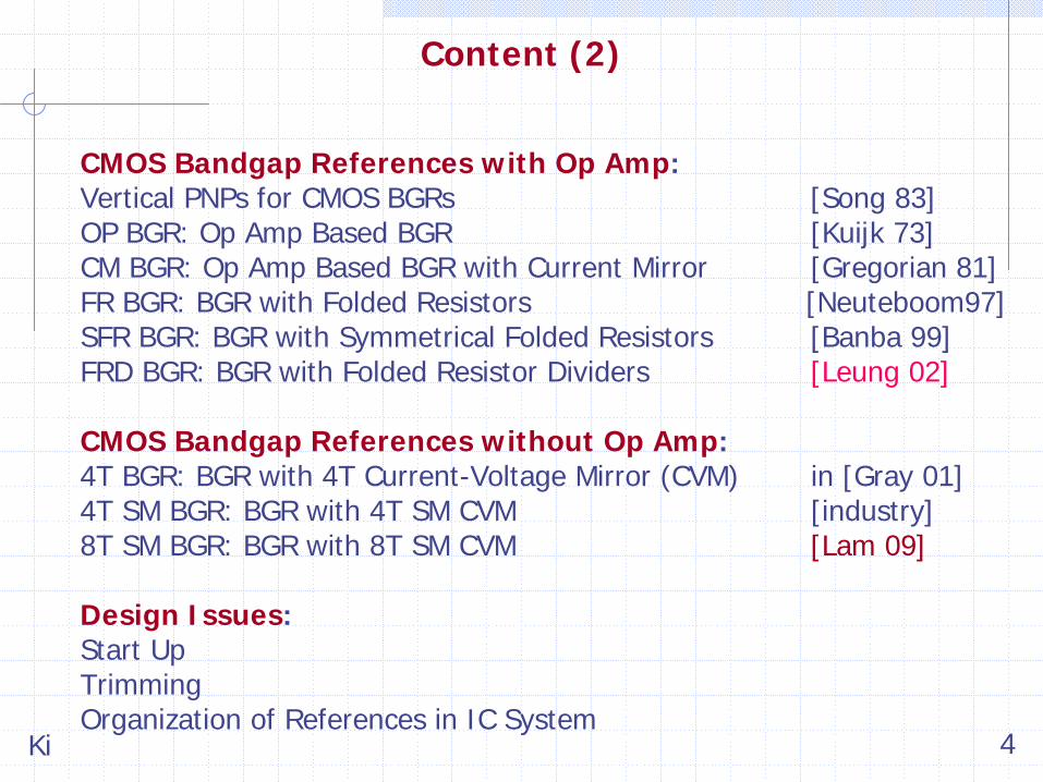
Ki 4
CMOS Bandgap References with Op Amp:Vertical PNPs for CMOS BGRs [Song 83]OP BGR: Op Amp Based BGR [Kuijk 73]CM BGR: Op Amp Based BGR with Current Mirror [Gregorian 81]FR BGR: BGR with Folded Resistors [Neuteboom97]SFR BGR: BGR with Symmetrical Folded Resistors [Banba 99]FRD BGR: BGR with Folded Resistor Dividers [Leung 02]
CMOS Bandgap References without Op Amp:4T BGR: BGR with 4T Current-Voltage Mirror (CVM) in [Gray 01]4T SM BGR: BGR with 4T SM CVM [industry]8T SM BGR: BGR with 8T SM CVM [Lam 09]
Design Issues:Start UpTrimmingOrganization of References in IC System
Content (2)

Ki 5
= −
= −
BE T
BE T
V /nVc s
V /nV2 ni
A B
I I (e 1)D
qn A (e 1)N W
I-V Characteristic of NPN
The I-V characteristic of a short-base npn transistor is [Sze 81]
where Ic : collector currentIs : reverse saturation currentVBE : base-emitter voltageVT : thermal voltage = kT/qk: Boltzmann’s constant (=1.38x10⁻²³ J/K)T: absolute temperature (Kelvin, K)q: electronic charge (=1.6x10⁻¹⁹ C)n: non-ideality factorni : intrinsic carrier concentrationA: area of baseDn : diffusion constant of electron (minority carrier) in the baseNA : donor (majority carrier) doping concentration in the baseWB : effective base width (to replace diffusion length)
eI
cI
E
BEV1Q
bIB
C

Ki 6
Temperature Dependence of I-V Curve
We investigate the temperature dependence of the transistor. With Einstein’s relation:
−
−η
= μ=
μ =Go T
2ns 1 iV /nV2 3
i 2
n 3
I C Tnn C T e
C T
= =μ μ
p n
p n
D D kTq
we have
−γ= = γ = − ηGo TV /nVs 1 2 3I CT e (C C C C , 4 )
and gives
where μn : (average, effective) mobility of electronVGo : silicon bandgap voltage at 0K (=-273oC) [Gray 01] gives VGo =1.205V with no explanation; while [Sze 81] gives VGo =1.17V, and VG (300k)=1.11V using experimental data.

Ki 7
Temperature Dependence of VBE
The temperature dependence of the collector current is quite complicated but could be expressed as [Gray 01]
⎛ ⎞= ⎜ ⎟
⎝ ⎠c
BE Ts
IV nV ln
I
χ=cI DT
and gives
( )γ−χ= −Go TV nV ln ET
= − γ − χ +Go TV nV [( ) ln(T) ln(E)]
χ
−γ
⎛ ⎞= ⎜ ⎟
⎝ ⎠Go TT V /nV
DTnV lnCT e
=(E C /D)
Note: (1) VBE is lower than VGo(2) Temperature coefficient (TC) of VBE (∂VBE /∂T) is negative

Ki 8
The thermal voltage at T = 300K (27oC) is
Realizing VREF
∂= =
∂T TV Vk
T q T−= + × 6 o86.25 10 V / C
The TC of VT at 300K is positive:
−
−
× ×= = =
×
23
T 19
kT 1.38 10 300V 25.88mVq 1.6 10
From previous page, we learn that TC of VBE is negative. If we design a circuit with a voltage proportional to VT , then we have
We need to determine the condition for VREF to have zero TC.
= − γ − χ + −Go T TV nV ( ) ln(T) V [M nln(E)]
= +REF BE TV V MV
Ki 9
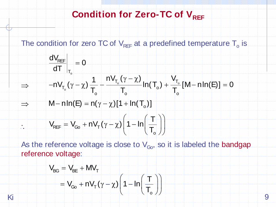
Condition for Zero-TC of VREF
The condition for zero TC of VREF at a predefined temperature To is
=o
REF
T
dV0
dTγ − χ
− γ − χ − + − =o o
o
T TT o
o o o
nV ( ) V1nV ( ) ln(T ) [M nln(E)] 0T T T
⇒
⇒ − = γ − χ + oM nln(E) n( )[1 ln(T )]
⎛ ⎞⎛ ⎞= + γ − χ −⎜ ⎟⎜ ⎟
⎝ ⎠⎝ ⎠REF Go T
o
TV V nV ( ) 1 lnT∴
As the reference voltage is close to VGo , so it is labeled the bandgap reference voltage:
= +BG BE TV V MV⎛ ⎞⎛ ⎞
= + γ − χ −⎜ ⎟⎜ ⎟⎝ ⎠⎝ ⎠
Go To
TV nV ( ) 1 lnT

Ki 10
Temperature Dependence of VBG
For T = To +ΔT and ln(1+δ) ≈ δ–½δ2, we have
⎛ ⎞Δ= +⎜ ⎟
⎝ ⎠oT To
TV V 1T
⎛ ⎞ ⎛ ⎞Δ Δ Δ= + ≈ −⎜ ⎟ ⎜ ⎟
⎝ ⎠ ⎝ ⎠
2
2o o o o
T T T 1 Tln ln 1T T T 2 T
⎛ ⎞Δ= + γ − χ −⎜ ⎟
⎝ ⎠o
2
BG Go T 2o
1 TV V nV ( ) 12 T
then
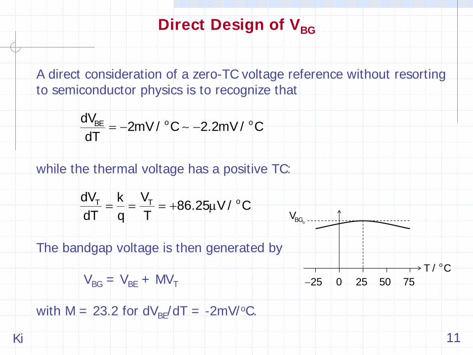
Hence, VBG peaks at VBGo = VBG (To ), and VBG (T) < VBG (To ):
oBGV
0 25−25 75
oT / C50
Ki 11
Direct Design of VBG
A direct consideration of a zero-TC voltage reference without resorting to semiconductor physics is to recognize that
= − −∼o oBEdV2mV / C 2.2mV / C
dT
while the thermal voltage has a positive TC:
= = = + μ oT TdV Vk86.25 V / C
dT q T
The bandgap voltage is then generated by
VBG = VBE + MVT
with M = 23.2 for dVBE /dT = -2mV/oC.
oBGV
0 25−25 75
oT / C50

Ki 12
TC of Voltage References
The IC industry defines TC of VREF as:
−=
−REF,max REF,min
2 1
| V V |TC
T Toin mV / C
oin ppm / C−=
−REF,max REF,min REF,ave
2 1
| V V | / VT T
Moreover, due to simulation and fabrication variations, the measured zero TC point may not be at exactly the midpoint of the temperature range:
1T oT 2T
REF,maxVREF,minV
REF,aveV
ΔTΔT

Ki 13
TC of BGR
For the ideal I-V curve with the temperature range of 2ΔT, the TC of VBG is given by
Δ= γ − χ
Δo
2
T 2o
1 T 1TC nV ( )2 2 TT
Let n(γ–χ) = 2, and To = 300K (27oC), then
= × × × ×2
2
1 50 1TC 2 25.88m2 100300
≈ μ o7.2 V / C
If the temperature range is from 250K (-23oC) to 350K (77oC), then To = 300K (27oC), ΔT = 50oC, T2 – T1 = 100oC, and
= + × ≈BGV 1.205 2 25.88m 1.26V
≈ o6ppm / CIn actual design, the TC figures would be (much) worse.

Ki 14
Line Regulation
• Find Vdd (min) such that the voltage reference is barely operative• Measure points range from Vdd (min)+0.2V to Vdd (max)• Compute line regulation
in mV / VΔ=Δ
REF
dd
Vline reg.
V
Line regulation is the change of VREF w.r.t. the change in Vdd :
Δ=
ΔREF REF
dd
V / VV
in % / V
Transistor circuits are non-linear circuits for large signal changes, and hand analysis is impossible. It could be obtained by simulation. In datasheets, line regulation is usually measured:

Ki 15
Power Supply Rejection
Power supply rejection (PSR) is the small signal change of VBG w.r.t. the small signal change in Vdd .
In transfer function form:
In dB:
Usually |vbg /vdd | < 1, but we customarily give a positive PSR in dB.
Note: Line reg. ≈
PSR × ΔVdd
= bg
dd
vPSR
v
= × dd
bg
vPSR 20 log
v
For a good voltage reference (also for bandgap reference and linear regulator), the output voltage should be a weak function w.r.t. the supply voltage. Hence, a small signal parameter, the power supply rejection, gives good indication of line regulation.

Ki 16
Load Regulation and Output Impedance
in mV /mAΔ=
ΔREF
o
Vload reg.
I
Load regulation is the change of VREF w.r.t. the change in Io :
Δ=
ΔREF REF
o
V / VI
in % /mA
In datasheets, load regulation is usually measured. Moreover, many BGRs cannot drive resistive loads, and load regulation is not included.
In the small signal limit, load regulation is the output impedance:
= REFo(REF)
o
dVR
dIΩin
Ki 17
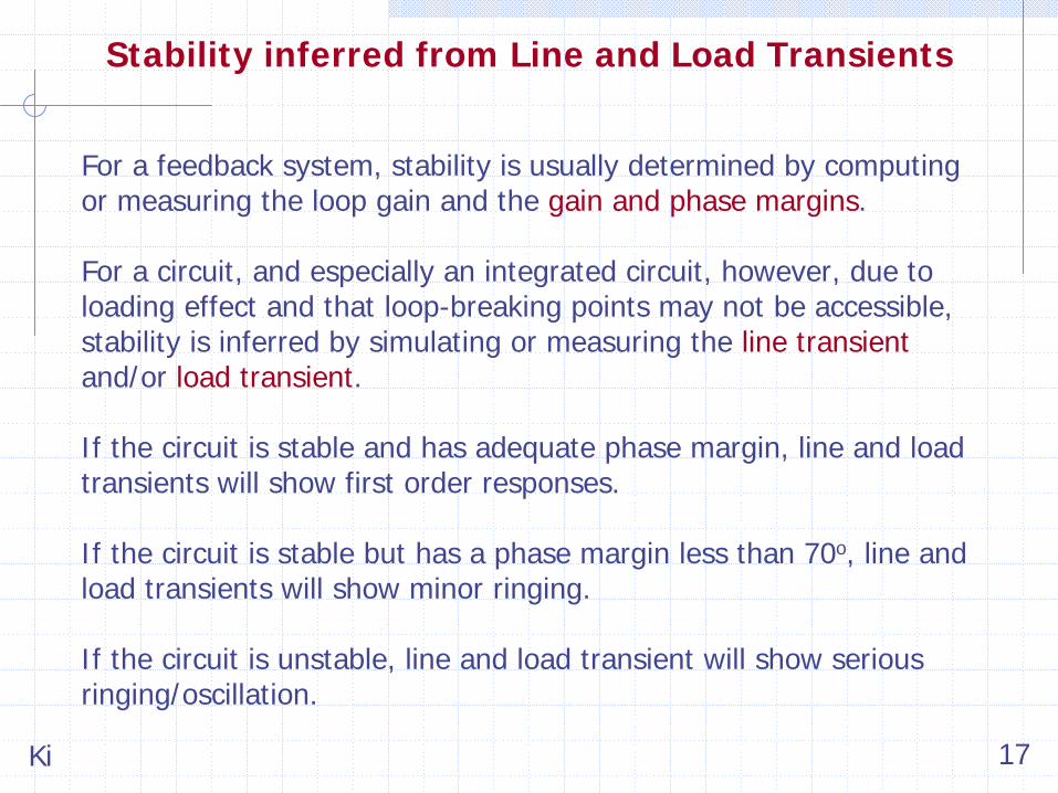
Stability inferred from Line and Load Transients
For a feedback system, stability is usually determined by computing or measuring the loop gain and the gain and phase margins.
For a circuit, and especially an integrated circuit, however, due to loading effect and that loop-breaking points may not be accessible, stability is inferred by simulating or measuring the line transient and/or load transient.
If the circuit is stable and has adequate phase margin, line and load transients will show first order responses.
If the circuit is stable but has a phase margin less than 70o, line and load transients will show minor ringing.
If the circuit is unstable, line and load transient will show serious ringing/oscillation.

Ki 18
Voltage References Criteria
A good voltage reference should have:
(1) Low TC over a wide range of temperature(2) Low line regulation and good power supply rejection (PSR)(3) Good stability
Other considerations:
(1) Low load regulation (if applicable)(2) Minimum Vdd for operation(3) Consume little power(4) Small area for resistors(5) Small area for compensation capacitor (if applicable)(6) Low noise(7) Long term stability
Ki 19
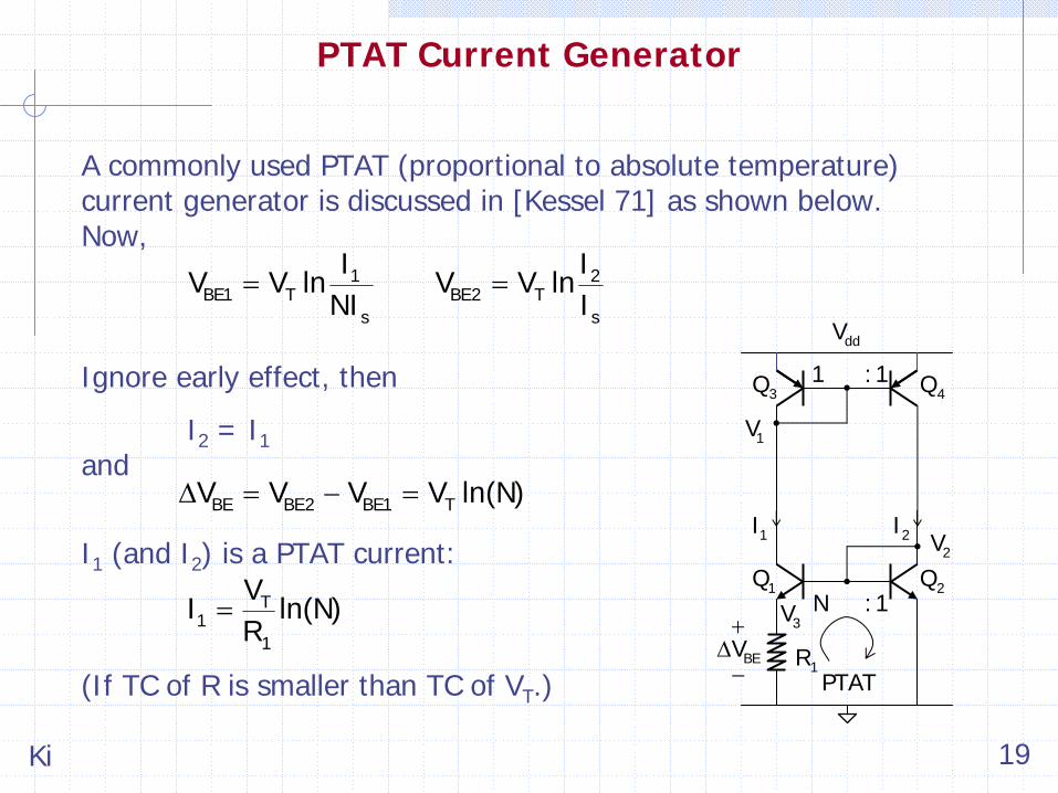
PTAT Current Generator
= 1BE1 T
s
IV V ln
NI= 2
BE2 Ts
IV V ln
I
Δ = − =BE BE2 BE1 TV V V V ln(N)
A commonly used PTAT (proportional to absolute temperature) current generator is discussed in [Kessel 71] as shown below.Now,
Ignore early effect, then
I2 = I1and
I1 (and I2 ) is a PTAT current:
= T1
1
VI ln(N)
R
1Q 2Q
1R
N :1
3Q 4Q
ddV
PTAT
1I 2I
1 :1
+Δ−
BEV
1V
3V
2V
(If TC of R is smaller than TC of VT .)

Ki 20
Basic BGR: Schematic
= +BG BE2 2 2V V I R
The simplest bandgap reference (BGR) consists of 4 transistors and 2 resistors. Positive TC is generated by the PTAT circuit consists of Q1 , R1 and Q2 (n=1 and large β) [Meijer 76]*. The reference voltage is
= + 2BE2 T
1
RV ln(N)V
R
1Q 2Q
1R
N :1
BGV
3Q 4Q
ddV
2R
PTAT
1I 2I
1 :1
+Δ−
BEV
1V
3V
2V
Clearly, VBE2 has a –ve TC, and VT has a +ve TC. Note that the TCs of R1 and R2 cancel each other. Also, the basic BGR, and all other BGRs, requires a start-up circuit (to be discussed later).
*The basic BGR is referenced, not proposed, in [Meijer 76].

Ki 21
To achieve zero TC for VBG at To , we set
= ⇒ + =o
o
TBG BE2 2
T 1 o
VdV dV R0 ln(N) 0
dT dT R T
R1 and R2 has the same TC, and (R2 /R1 )×ln(N) is independent of temp. In practice, TC of VBE2 is obtained by characterizing the process, and
≈ − −o oBEdV2mV / C to 2.2mV / C
dT
The transistor ratio N is usually taken as 4 or 8, and I1 is determined by the application, usually ranges from 10μA to 100μA. Let TC of VBE be -2mV/oC (from measurement), and To =300K, then
−
−
× × ×= = = ≈
×
22o2
231 T
2m TR 2m q 3.2 10ln(N) 23.2R V k 1.38 10
Basic BGR: Zero TC Condition

Ki 22
Common centroid layout for Q1 and Q2 for better matching:
2Q1Q
Q1 :Q2 = 4:1 Q1 :Q2 = 8:1
= = ΩT1
1
VR ln(N) 10.76k
I
Take N=8, ΔVBE = VT ln(N) = 53.8mV at T=300K. For I1 =5μA,
× ×= = × × = Ωo 1
2 o 1T
2m T RR 2m T I 120k
V ln(N)
Basic BGR: Matching Consideration
1Q
1Q
1Q 2Q1Q
1Q
1Q
1Q
1Q1Q
1Q 1Q
N.B. Some designs use N > 100 to generate a large ΔVBE for better (lower) sensitivity due to process variations.

Ki 23
Process and Simulation
Process: TSMC 0.18μ
deep n-well CMOSNMOS: Vtn =0.44VPMOS: |Vtp |=–0.44Vnpn: VBE (4.7μA)=0.70Vpnp: VEB (4.7μA)=0.64V
Conditions: N=8, I1 ≈4.6μA @25oC, R1 =10.8kΩ, R2 =91.6kΩ
Notes:
(1) All voltage references in this talk are simulated using the same 0.18μ
CMOS process that also supports bipolar transistors.
(2) With N=8, R2 should be 11.16×R1 = 120.5kΩ, but as the non- ideality factor n ≠
1, R2 needed is smaller.
(3) Current mirrors are simulated using PMOS transistors.
(4) I thank Mr. Chenchang Zhan for assisting in all Spice simulations.

Ki 24
Basic BGR: TC + Line Reg. Simulation
1.135V1.130V1.125V1.120V1.115V
2.7V
1.110V
1.140V
− o25 C o0 C o25 C o50 C o75 C
2.2V
=ddV 1.7V
BGV
T
Instead of cutting and pasting the simulation results, they are redrawn using PowerPoint as shown below. Note that line regulation causes a larger error than the temperature dependence.

Ki 25
Cross-Biased 4T Cell
The loop gain of the basic BGR is independent of R2 . Moreover, for N = 1 and R1 = 0Ω, T = -1, and the circuit oscillates.
Although the circuit oscillates, this cross-biased 4T cell, when properly connected, can be considered as a current mirror as well as a voltage mirror: current conveyer [Smith 68], or current-voltage mirror (CVM) [Lam 08]. More on this later.
1Q 2Q:1
3Q 4Q
ddV
1I 2I
1 :1
1V
2V
11M 2M
:1
3M 4M
ddV
1I 2I
1 :1
1V
2V
1
UNSTABLE by
themselves!
But could be useful if
properly connected.

Ki 26
Basic BGR: PSR Analysis
Small signal model for computing PSR of the basic BGR:
1R
1v
2v
bgv
π1r π2r
π3r π4r
2R
m21 / g
−m4
dd 1
g(v v )
−m1
2 3
g(v v )
ddv
m31 / go3r o4r
3vo1r o2r
⎛ ⎞⎛ ⎞= = + +⎜ ⎟⎜ ⎟⎜ ⎟+⎝ ⎠⎝ ⎠
bg on2
dd 1 op on m op on
v rR 1 1PSR 1 ln(N)v R r r ln(N) g (r || r )
The computation is not trivial, but using appropriate approximations, it could be shown that, for ron =ro1,2 , rop =ro3,4 ,

Ki 27
Basic BGR: Line Transient
1.41.6
2.01.8
t / sμ10 μ20
BGV
ddV
μ30
Assume on-chip application such that CLoad =10pF. The basic BGR is stable with a larger CLoad .
t / sμ10 μ20 μ30
1.12
1.14
1.10

Ki 28
Basic BGR: Performance Summary
Parameter Computation Simulation SimulationBSIM 3 Level 1(βn =20) (βn =80)
R2 (R1 =10.8kΩ) 120.5kΩ
91.6kΩ
108.3kΩVdd (min)=VBG +0.2V 1.45V 1.5V 1.5VVBG (Vdd =1.7V) 1.118V 1.118VTC 6ppm/oC 49ppm/oC 8ppm/oCLoop gain -0.324 -0.349 -0.324PSR 32.7dB 33.6dB 32.4dBLine regulation 23mV/V 22mV/V 25mV/V
N.B.(1) R2 is smaller than computed because n (ideality factor) is not 1.(2) BSIM3 simulation using parasitic Q1 and Q2 gives a much larger
TC than predicted in pp.13. By substituting Q1 and Q2 with Level 1 npn with βn =80, TC simulation is close to prediction.

Ki 29
Symmetrical Matching of Bipolar Transistors
When a pair of bipolar transistors Q1 and Q2 of the same type are matched, the area ratio is designed to be the same as the intended current ratio. However, their collector-emitter voltages may be different and their collector currents are different due to early effect.
If Q1 and Q2 are forced (by an additional circuit) to have essentially the same VC , VB and VE , then they are called symmetrically matched (SM) [Lam 07b].
High performance BGRs inevitably employ symmetrical matching to improve PSR, although not explicitly stated [Brokaw 74].

Ki 30
Basic SM BGR
1Q 2Q
1R
N :1
BGV
3Q4Q
ddV
2R
1I 2I
1 :1
+Δ−
BEV
4V
3V
2V
5Q
6Q
3I
1
1V
5V
2R
For the basic BGR, line regulation and PSR could be improved by reducing the early effect of Q1 and Q2 . The Q5 and Q6 branch is added, forcing Q1 and Q2 to be symmetrically matched. By adding R2 at the collector of Q3 , Q3 and Q4 are symmetrically matched.
The reference voltage is
= − = ×2om op on
2i
vT ln(N) g (r || r )
v
where all transistors have the same transconductance gm , all npn have the same ron , and all pnp have the same rop . This T is –ve feedback.
= + 2BG BE5 T
1
RV V ln(N)V
R
The loop gain at breaking at V2 is
cC

Ki 31
Basic SM BGR (2)
1Q 2Q
1R
N :1
3Q 4QddV
1I 2I
1 :1
+Δ−
BEV
4V
3V
2V
5Q
6Q
3I
1
1V
cC 7Q
BGV
8Q
2R4I
+
−BE7V
To save a large R2 , a fourth branch (Q7 and Q8 ) could be added, and
= + 2BG BE7 T
1
RV V ln(N)V
R
:1
N.B. Both basic SM BGRs are used in the industry but not discussed in the literature.

Ki 32
Basic SM BGR: Performance Summary
Parameter Computation Simulation SimulationBSIM 3 Level 1(βn =20) (βn =80)
R2 (R1 =10.8kΩ) 120.5kΩ
115.4kΩ
105.7kΩVdd (min) 1.45V 1.5V 1.3VVBG (Vdd =1.7V) 1.3305V 1.3305VTC 6ppm/oC 13.3ppm/oC 5.9ppm/oCLoop gain 64.5dB 60.9dB 64.1dBPSR 69dB 60dBLine regulation -0.36mV/V -0.83mV/V
N.B. TC performance of the basic SM BGR is closer to prediction even for BSIM3 simulation using parasitic Q1 and Q2 .

Ki 33
The op-amp based bandgap was first discussed in [Kuijk 73] using Widlar current source [Widlar 65] with I1 ≠I2 . For I1 =I2 , Q1 and Q2 will have different sizes (N:1). The op-amp A(s) forces I1 =I2 , and I1 is a PTAT current:
1Q 2Q
1R
2R1I
BGV
ddV
−+
N :1
2R=2 1I I− = =BE2 BE1 T 1 1V V V ln(N) I R
= +BG BE2 1 2V V I R
= + 2BE2 T
1
RV ln(N)V
R
This VBG relation is the same as that of the basic BGR. However, the total resistance is
RT = R1 + 2R2 .
EA
Op-Amp Based BGR (OP BGR)

Ki 34
In a digital CMOS n-well process, parasitic lateral pnp, lateral npn and vertical pnp transistors could be identified. Vertical pnp transistors are more commonly used for their lower base resistance than lateral transistors. However, the collector, which is the p-sub, is restricted to be connected to ground.
BJTs in Digital CMOS Process
−n well
+n+p+p
p-sub
+p+n+n
lateralpnp
verticalpnp
BB
C
CE E
B
CE+p
lateralnpn
GND GND GNDEV
Parasitic vertical pnp transistors were used in [Song 83].

Ki 35
1Q
N :1
1R
2R2R
BGV
A(s)
+T−T
PTAT
1I 2I
2Q
Op-Amp Based BGR (OP BGR)
For a standard CMOS digital process, BGR usually uses parasitic vertical pnp transistors. By drawing the CMOS op-amp based BGR (OP BGR) as shown on the right, two feedback loops, one negative and one positive, can easily be identified.
1Q 2Q
1R
2R1I
BGV
ddV
−+
N :1
2R1I
aV
aV
− +
EA
This BGR can drive resistive load if EA is properly designed.

Ki 36
OP BGR: –ve and +ve Feedback Loops
Negative feedback loop:
−+
= ×+ +
m1 1
m1 1 2
1 g RT A(s)
1 g (R R )
Positive feedback loop:
+−
= ×+ m1 2
1T A(s)
1 g R
For stability, we need |T- | > |T+ |, and this criterion is satisfied by the above two relations.
The above T- and T+ ignore parasitic capacitors of the transistors and resistors. By accounting for all parasitics, we require |T- (jω)| > |T+ (jω)| for all frequencies.
+| T (s) |
−| T (s) |
f

Ki 37
OP BGR: System Loop Gain
By breaking the loop at the output of the op-amp Va , the system loop gain T(s) is given by
− += −T T T
⎛ ⎞+= − ×⎜ ⎟+ + +⎝ ⎠
m1 1
m1 1 2 m1 2
1 g R 1 A(s)1 g (R R ) 1 g R
Stability of a system is determined by the system loop gain, however, parasitic capacitors complicate the loop gain expression, and may not be too useful in compensation consideration:
⇒
Considering T- (s) and T+ (s) for stability is more direct.
An example is shown in designing the current-mirror (CM) BGR.
Ki 38
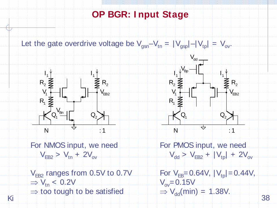
OP BGR: Input Stage
Let the gate overdrive voltage be Vgsn –Vtn = |Vgsp |–|Vtp | = Vov .
1Q 2Q
1R
2R1I
N :1
2R1I
1V EB2V
BnV
For NMOS input, we needVEB2 > Vtn + 2Vov
VEB2 ranges from 0.5V to 0.7V ⇒
Vtn < 0.2V⇒
too tough to be satisfied
For PMOS input, we needVdd > VEB2 + |Vtp | + 2Vov
For VEB =0.64V, |Vtp |=0.44V, Vov =0.15V⇒
Vdd (min) = 1.38V.
1Q 2Q
1R
2R1I
2R1I
1V
BpV
N :1
ddV
EB2V

Ki 39
OP BGR: Example
1Q 2Q
1R
2R
N :1
2R
ddV
2M1M
BGV
zM5M
cC4M3M
7M
6M
The OP BGR could be implemented by a 2-stage op-amp with a self- biasing scheme, and it resembles the CM BGR to be discussed in terms of feedback connections. Note that a start-up circuit is needed.
−V +V

Ki 40
OP BGR: Offset Error
1Q 2Q
1R
2R1I
BGV
ddV
−+
N :1
2R2I
aV+ −
osVEB2V
1V
+
−EB1V
For a bipolar op-amp, the offset voltage could be as low as 1mV, while for a CMOS op-amp, the offset voltage could be a few mV.
⎛ ⎞= + − +⎜ ⎟
⎝ ⎠2 2
BG EB2 T os1 1
R RV V ln(N)V 1 V
R R
By accounting for Vos , it can be shown that [Song 83]
EA

Ki 41
CM BGR: Offset Error
The op amp may drive a current mirror instead of the resistors directly [Gregorian 81]. The BGR is thus called the current-mirror BGR (CM BGR). The current mirror forces the drain currents of M1 and M2 to be equal, and
1Q 2Q
:N
1R
2R2R
BGV
A(s) 1I
ddV
1
2M1M
osV
+ −
1I
EB2V
+
−EB1V
1V
= + × + ×2 2BG EB2 T os
1 1
R RV V ln(N) V V
R R
Hence, the effect due to Vos is smaller and opposite to that of the OP BGR.
In principle, R2 at M1 may be eliminated to save a resistor, but channel length modulation of M1 and M2 affects accuracy.
+ −
aV

Ki 42
T+ and T– of CM BGR
:N
1R
2R2R
BGV
A(s) 1I2I
Note that Vd1 and Vd2 generate the same reference voltage, but the reference output should be taken at Vd2 , because with the filtering capacitor COUT , the positive feedback loop then has an even lower gain at high frequencies, satisfying |T- (jω)| > |T+ (jω)|.
ddV
1
2M1M
1V
d2V
With a PMOS input stage, andVEB2 = 0.64V|Vtp | = 0.44VVov = 0.15V
The minimum Vdd is thus
Vdd (min) = VBE2 +|Vtp |+2Vov = 1.38VOUTC
1Q 2Q+
−EB1V
d1V
EB2V

Ki 43
CM BGR: Line Transient with cap. at Vd1
3.0Vt / s
μ5 μ5.2
ddV
f /Hz
dB
60
40
20
−20
0
10G100k 10M 100M1M 1G
−T+T
3.3V
If COUT is connected at Vd1 , then |T+ (jω)| > |T- (jω)| at high frequencies, making the BGR unstable.
1.2Vt / s
μ5 μ5.2
d1V1.3V
t / sμ5 μ5.2
1.2V
1.4V d2V

Ki 44
CM BGR: Line Transient with cap. at Vd2
3.0Vt / s
μ5 μ5.2
ddV
f /Hz
dB
60
40
20
−20
0
10G100k 10M 100M1M 1G
−T
+T
3.3V
If COUT is connected at Vd2 , then |T+ (jω)| < |T- (jω)| for all frequencies, and the BGR is stable.
1.2Vt / s
μ5 μ5.2
d1V
t / sμ5 μ5.2
1.22V
1.4V
d2V1.28V

Ki 45
CM BGR with PMOS Input
1Q 2Q
1R
2R1I
2R1I
1V
N :1
ddV
EB2V
BGVAV
−V +VOUTC
A 2-stage op amp could be used, and biased by the PTAT circuit.
cR cC

Ki 46
CM BGR: Performance Summary
Parameter Computation SimulationBSIM 3
R1 12kΩ
12kΩR2 133.9kΩ
123.1kΩRT 279.8kΩ
258.2kΩIpnp 4.75μA 4.75μAIop 9.5μA 9.5μAItotal 19μA 19μACc 200fF
Vdd (min) 1.38V 1.5VVBG (Vdd =1.7V) 1.2757VTC 6ppm/oC 7.26ppm/oCPSR 79dBLine regulation +0.12mV/V
Ki 47
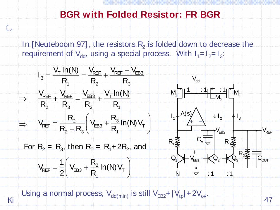
BGR with Folded Resistor: FR BGR
In [Neuteboom 97], the resistors R2 is folded down to decrease the requirement of Vdd , using a special process. With I1 =I2 =I3 :
1Q 2Q
N
1R
A(s)1I 2I
ddV
2M1M
OUTC+
−EB1V
+ −
3Q
3I
3M
REFV
2R
EB2V
1 :1 :1
3R
−= = + REF EB3T REF
31 2 3
V VV ln(N) VI
R R R
+ = +EB3REF REF T
2 3 3 1
VV V V ln(N)R R R R
:1 :1
⎛ ⎞= +⎜ ⎟+ ⎝ ⎠
32REF EB3 T
2 3 1
RRV V ln(N)V
R R R⇒
⇒
For R2 = R3 , then RT = R1 +2R2 , and
⎛ ⎞= +⎜ ⎟
⎝ ⎠2
REF EB3 T1
R1V V ln(N)V2 R
Using a normal process, Vdd(min) is still VEB2 +|Vtp |+2Vov .
−VC
Ki 48
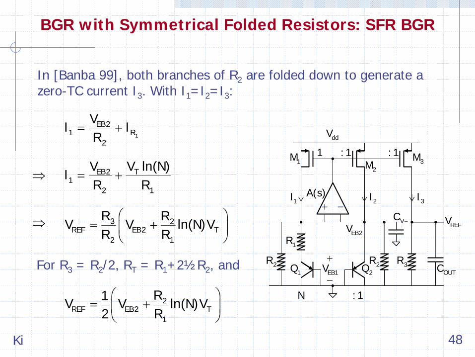
In [Banba 99], both branches of R2 are folded down to generate a zero-TC current I3 . With I1 =I2 =I3 :
BGR with Symmetrical Folded Resistors: SFR BGR
1Q 2Q
N
1R
A(s)1I 2I
ddV
2M1M
OUTC+
−EB1V
+ − 3I
3M
REFV
2R
EB2V
1 :1 :1
:1
2R 3R
= +1
EB21 R
2
VI I
R
= +EB2 T1
2 1
V V ln(N)I
R R⇒
⎛ ⎞= +⎜ ⎟
⎝ ⎠3 2
REF EB2 T2 1
R RV V ln(N)V
R R⇒
For R3 = R2 /2, RT = R1 +2½R2 , and
⎛ ⎞= +⎜ ⎟
⎝ ⎠2
REF EB2 T1
R1V V ln(N)V2 R
−VC

Ki 49
In [Neuteboom 97], the 0.8μ
process has |Vtp |=-0.7V and Vtn =0.5V. Due to low Vtn , the op amp has an NMOS input stage, and
Vdd (min) = VREF + Vov
For VREF =670mV, the BGR works at Vdd =0.9V or lower.
In [Banba 99], the 0.4μ
n-well process has |Vtp |=-1V, Vtn =0.7V, and native NMOS with Vtn(native) =-0.2V. The op amp uses a native NMOS input stage, and
Vdd (min) = VREF + Vov
For VREF =515mV, the simulated lowest Vdd is 0.84V. However, all measurements in [Banba 99] used Vdd are larger than 2.4V.
FR BGR and SFR BGR with Sub-1V Operation
Ki 50
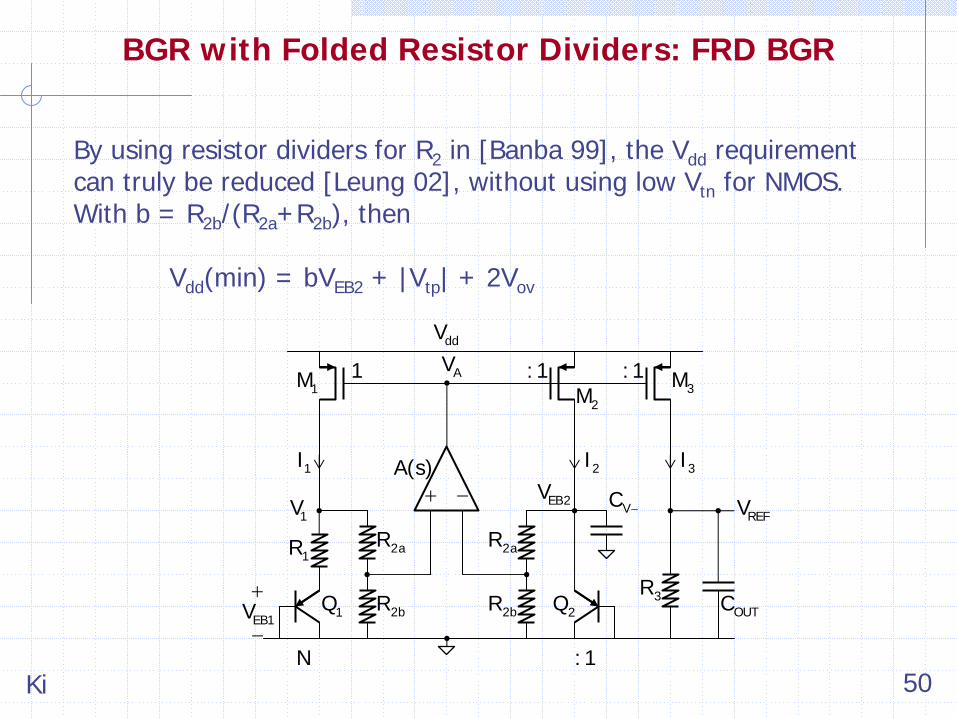
BGR with Folded Resistor Dividers: FRD BGR
1Q 2Q
N
1R
A(s)1I 2I
ddV
2M1M
OUTC+
−EB1V
+ − 3I
3M
REFV
2bR
EB2V
1 :1 :1
:1
2aR
3R
2aR
2bR
1V
AV
By using resistor dividers for R2 in [Banba 99], the Vdd requirement can truly be reduced [Leung 02], without using low Vtn for NMOS. With b = R2b /(R2a +R2b ), then
Vdd (min) = bVEB2 + |Vtp | + 2Vov
−VC

Ki 51
SFR/FRD BGR: Performance Summary
Parameter SFR BGR FDR BGR
R1 25kΩ
25kΩR2 269.4kΩ
268.5kΩ
(b=0.6)R3 126kΩ
125.5kΩRT 689.8kΩ
687.5kΩIpnp 4.75μA 4.75μACVBE2 5pF 5pFCc / Rc 60fF / 12kΩ
60fF / 12kΩItotal 24.25μA 24.25μA
Vdd (min) 1.4V 1.2VVBG 0.6015V 0.6003VTC 4.32ppm/oC (Vdd =1.8V) 6.1ppm/oC (Vdd =1.5V)PSR 84.7dB 96.5dBLine reg. -0.12mV/V -0.12mV/V

Ki 52
PTAT loop is realized by forcing VEB1 +I1 R1 (=Vy ) = VEB2 (=Vx ). The previous BGRs use an op-amp, but we may use a “voltage mirror” instead. The cross-biased 4T cell with the PMOS side connected to Vdd is such a voltage mirror.
A positive feedback loop is identified and the diode-connection must be at Rx with Rx <Ry to maintain stability.
The loop gain is
Cross-Biased 4T Cell
n1Mn2M:1
p1Mp2M
ddV
1I2I
1 :1
1V
2V
1
xRXVyV
yR
1iV 1oV
+= − = −
+1o mn x
1i mn y
V 1 g RT
V 1 g R

Ki 53
BGR with 4T Current-Voltage Mirror
n1Mn2M:1
p1Mp2M
ddV
1I2I
1 :1
1V
2V
1
1Q
1R
+
−EB1V 2Q
:1N
zQ
2R
pzM
BGV
XVyV
+
−EB2V
+= − = −
+ +1o mn x
1i mn 1 x
V 1 g RT
V 1 g (R R )
where Rx =1/gmq , with gmq the transconductance of all pnp transistors, and
Vdd(min) = VEB2 +Vtn +2Vov
The 4T current-voltage mirror (CVM) forces Vy =Vx , and Q1 , R1 and Q2 forms a PTAT loop with
= = T1 2
1
VI I ln(N)
R
The reference voltage is thus
:1
= + ×2BG EBZ T
1
RV V ln(N) V
R
The loop gain of the 4T BGR is
zV
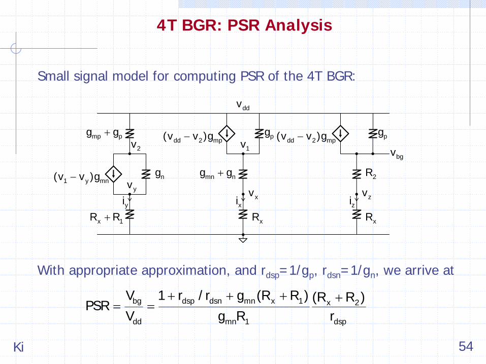
Ki 54
4T BGR: PSR Analysis
+ + + += =bg dsp dsn mn x 1 x 2
dd mn 1 dsp
V 1 r / r g (R R ) (R R )PSR
V g R r
Small signal model for computing PSR of the 4T BGR:
With appropriate approximation, and rdsp =1/gp , rdsn =1/gn , we arrive at
2R
xR xRxiyi zi
+x 1R R
+mp pg g −dd 2 mp(v v )g−dd 2 mp(v v )g
ddv
pg pg
ng
bgv
−1 y mn(v v )g +mn ng g
2v
yv
1v
xv zv

Ki 55
4T SM BGR
p3M
1Q2Q
zR
ddV
1R
:1 :N
BGV
pzM
s3M
n2M
zQ3Q
1 :1
By adding the Mn3 and Mp3 branch, Mn1 and Mn2 are symmetrically matched. The diode-connection of NMOS is at Q1 rather than at Q2 to give negative feedback, and Cc is added for compensation [industry].
n1Mn3M
p1M p2M
s2M
s1M
zVyVxVcC
−start up
[industry]: circuit not published but used in the industry.

Ki 56
8T SM BGR
1Q 2Q
zR
ddV
1R
:1
N
BGV
pzM
n4M
zQ
:1
n1M
p4M
zVyV xV
p3Mp1M
n2M
p2M
n3M
K :K:1
:1
+: K 1
1V2V
3V4V
Another way to achieve symmetrical matching is to use an 8T SM CVM [Taylor 99]. A modified version is shown below [Lam 08]. For stability, we require K>1, and a suggested value is K=4.
yI xI
xAI xBIyAIyBI

Ki 57
8T SM BGR: Operation
When the PTAT loop is activated, the current IX flows in Q2 is equal to IXA +IXB .
The W/L ratio of Mp1 and Mp3 is 1:K, and IXB is approximately equal to K×IXA (Mp1 and Mp3 are not symmetrically matched).
To provide the correct gate drive for Mp3 , the feedback action of the SM CVM drives V2 to be essentially equal to V1 , such that the X branch is symmetrically matched to the Y branch.
Now, with VSG of Mp1 being equal to VSG of Mp2 , Mp1 is then symmetrically matched to Mp2 .
Arguing in a similar fashion, we conclude that all transistor pairs (Mn1 , Mn2 ), (Mp1 , Mp2 ), (Mn3 , Mn4 ) and (Mp3 , Mp4 ) are symmetrically matched and thus VY =VX .
Ki 58
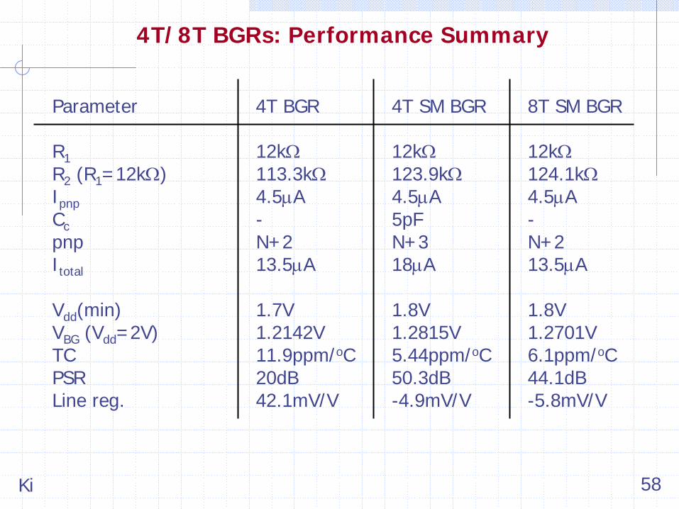
4T/8T BGRs: Performance Summary
Parameter 4T BGR 4T SM BGR 8T SM BGR
R1 12kΩ
12kΩ
12kΩR2 (R1 =12kΩ) 113.3kΩ
123.9kΩ
124.1kΩIpnp 4.5μA 4.5μA 4.5μACc - 5pF -pnp N+2 N+3 N+2Itotal 13.5μA 18μA 13.5μA
Vdd (min) 1.7V 1.8V 1.8VVBG (Vdd =2V) 1.2142V 1.2815V 1.2701VTC 11.9ppm/oC 5.44ppm/oC 6.1ppm/oCPSR 20dB 50.3dB 44.1dBLine reg. 42.1mV/V -4.9mV/V -5.8mV/V

Ki 59
Modified Widlar BGR
Widlar’s original BGR [Widlar 71] has minor matching difficulties. A modified version with better matching is shown below [Gilbert 96].
1Q 2Q
1R
N :1
BGV
ddV
2R
1I 2I2R
3Q
4Q3I

Ki 60
Brokaw BGR (1)
The Brokaw BGR is a popular topology for BJT process [Brokaw 74], and its CMOS variant is discussed in [Vittoz 79].
1Q 2Q
1RN :1
R
2R
+−
R
= + 2BG BE2 T
1
RV V 2 ln(N)V
R
1Q 2Q
1RN :1
2R
BGV
REFV
3R
BR
AR
⎛ ⎞= +⎜ ⎟⎝ ⎠
AREF BG
B
RV 1 V
R
BGV
To compensate for base current error, set
=+
1 A B3
2 A B
R R RR
R R R
3Q 4Q
5Q
ddV ddV

Ki 61
Brokaw BGR (2)
To achieve symmetrical matching between Q3 and Q4 , Q6 is added [Brokaw 74].
1Q 2Q
1RN :1
2R
BGV
REFV
3R
BR
AR
ddV
3Q 4Q
5Q
6Q
cC
1 : AB2R
B1R
1 :1
BI7Q
B4QB3Q
B2QB1Q
B5QQB1 , QB2 and RB2 forms a PTAT loop to produce IB , a PTAT current. QB3 and QB4 are used to minimize base current error. IB is at least 3 times of IPTAT , to supply enough base current to Q7 to drive resistive load.
PTATI

Ki 62
The basic BGR has two stable operation points:(1) Normal mode with VBG ≈
1.2V; and(2) Shutdown mode with V1 = Vdd and V2 = 0.
A start-up circuit should(1) automatically steer the BGR from the shutdown
mode to the normal mode;(2) disconnect from the BGR when it is working in
the normal mode; and(3) consume very little power.
Start-Up Consideration
1Q 2Q
1R
N :1
BGV
3Q 4Q
ddV
2R
PTAT
1I 2I
1 :1
+Δ−
BEV
1V
3V
2V

Ki 63
Basic BGR with CMOS Start-Up
1Q 2Q
1R
N :1
BGV
3M 4M
ddV
2R
1I 2I
1 :1
1V
3V
2V
s1Ms3M
s2M
long
wide
Consider the 0.18μ
CMOS process that supports bipolar transistors.
When BGR is shut down, V1 = Vdd , Ms1 is off and Ms2 is on, such that Vs is low, turning on Ms3 that pumps current to Q2 . Q1 mirrors current to turn on M3 , and M4 mirrors current and the BGR works properly.
Ms1 should be turned on hard by V1 , trying to source large current that puts itself into the linear region with a very small Vsd1 , such that Ms3 is shut off and isolated from the BGR.
sV
−start up
Ki 64
CMOS Start-Up Schemes
s1Ms3M
s2Mlong
wide
sV
−P startup
s1M
s3M s2M
long
wide
sV
−N startup
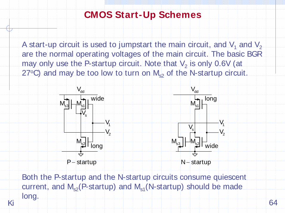
A start-up circuit is used to jumpstart the main circuit, and V1 and V2 are the normal operating voltages of the main circuit. The basic BGR may only use the P-startup circuit. Note that V2 is only 0.6V (at 27oC) and may be too low to turn on Ms2 of the N-startup circuit.
1V 1V
2V2V
ddVddV
Both the P-startup and the N-startup circuits consume quiescent current, and Ms2 (P-startup) and Ms1 (N-startup) should be made long.
Ki 65
Trimming for Zero-TC
Consider the Brokaw BGR. The simulated BGR has zero-TC, giving, say, VBG =1.263V at 25oC, and RA and RB are adjusted to give, say, VREF =2.50V. Due to inaccurate modeling and process variations, the fabricated BGR will have a different VREF and large TC.
A very accurate VREF will need to trim for both zero-TC and accurate initial value. The zero-TC point is determined by R1 :R2 , while the initial accuracy of VREF (at room temp.) is determined by RA :RB .
Trimming individual BGR for zero-TC is too time consuming. In practice, the zero-TC point is determined by fabricating and measuring the BGRs a few times using the same vendor and process. After finding the “optimal” ratio of R1 :R2 , this is then fixed for mass production and individual BGR will only be trimmed for initial accuracy.
Ki 66
Trimming for Initial Accuracy
For VREF =2.50V±1% over T and Vdd , the initial accuracy should be VREF = 2.50V±0.25% by trimming RB . The LSB of 0.25% is 6.25mV, and for 4-bit trimming, the trimming range is ≈±50mV.
Let IREF =5μA, such that RA =247.4kΩ
and RB =252.6kΩ±10kΩ. RB is divided into RB1 =242.6kΩ
and RB2 =18.75kΩ. RB2 consists of 4 smaller resistors of 1.25kΩ
(LSB), 2.5kΩ, 5kΩ
and 10kΩ
(MSB) that are connected in parallel with poly fuses (≈100Ω).
If the fabricated BGR behaves as designed, only 1 fuse (MSB fuse) is needed to be blown open. Otherwise, the BGR could still be trimmed up and down +43.75mV/-50mV.

Ki 67
Trimming Circuit
Trimming is usually done during wafer testing. A poly fuse of around 100Ω
needs 60mA to be blown open.
For RLSB >>Rpoly : blow fuse to trim up.
B1R
AR
Ω1.25k
Ω2.5k
Ω5k
Ω10k
6V(fromtester)
poly fuse
trim pad
thick metal
trim pad
trimpads
GNDpad
BGV
REFV
MSB
LSB

Ki 68
Organization of BGRs in IC Systems
For a low-voltage system, e.g., Vdd =5V, there is usually only one trimmed voltage reference.
For a system with Vdd =15V, there are usually two voltage references, one trimmed for accuracy, and a second one untrimmed and could work at very low voltage for start-up, UVLO (under voltage lockout) and OVP (over voltage protection).
untrimBGR
trimmedBGR
15V
BG(untrim)V
5V
+_
functionalblocks
REFV
UVLO OVP
linear regulator
Ki 69
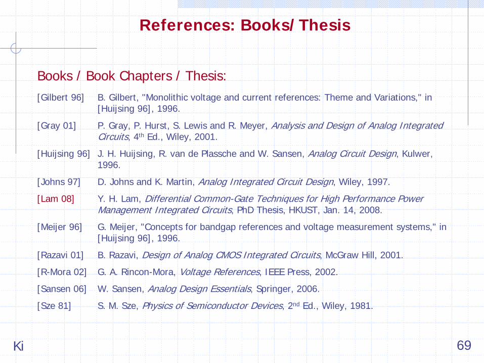
References: Books/Thesis
Books / Book Chapters / Thesis:[Gilbert 96] B. Gilbert, "Monolithic voltage and current references: Theme and Variations," in
[Huijsing 96], 1996.
[Gray 01] P. Gray, P. Hurst, S. Lewis and R. Meyer, Analysis and Design of Analog Integrated Circuits, 4th Ed., Wiley, 2001.
[Huijsing 96] J. H. Huijsing, R. van de Plassche and W. Sansen, Analog Circuit Design, Kulwer, 1996.
[Johns 97] D. Johns and K. Martin, Analog Integrated Circuit Design, Wiley, 1997.
[Lam 08] Y. H. Lam, Differential Common-Gate Techniques for High Performance Power Management Integrated Circuits, PhD Thesis, HKUST, Jan. 14, 2008.
[Meijer 96] G. Meijer, "Concepts for bandgap references and voltage measurement systems," in [Huijsing 96], 1996.
[Razavi 01] B. Razavi, Design of Analog CMOS Integrated Circuits, McGraw Hill, 2001.
[R-Mora 02] G. A. Rincon-Mora, Voltage References, IEEE Press, 2002.
[Sansen 06] W. Sansen, Analog Design Essentials, Springer, 2006.
[Sze 81] S. M. Sze, Physics of Semiconductor Devices, 2nd Ed., Wiley, 1981.

Ki 70
References: Current Sources
Current Sources and Circuits:[Frederiksen 72] T. M. Frederiksen, "Constant current source," US Patent 3,659,121, Apr. 25,
1972.
[Lam 07] Y. H. Lam, W. H. Ki and C. Y. Tsui, "Symmetrically matched voltage mirrors and applications therefor," US Patent 7,215,187, May 8, 2007.
[Kessel 71] T. van Kessel and R. van der Plaasche, "Integrated linear basic circuits," Philips Tech. Rev., pp.1-12, 1971.
[Smith 68] K. C. Smith and A. Sedra, "The current conveyor: a new circuit building block," Proc. of the IEEE., pp.1368-1369, 1968.
[Widlar 65] R. J. Widlar, "Some circuit design techniques for linear integrated circuits," IEEE Trans. Circ. Theory, pp.586-590, 1965.

Ki 71
Bandgap References:[Banba 99] H. Banba et. al., "A CMOS bandgap reference circuit with sub-1-V operation," IEEE
J. on Solid-State Circ., pp.670-674, May 1999.
[Brokaw 74] A. P. Brokaw, "A simple three-terminal IC bandgap reference," IEEE J. on Solid- State Circ., pp.388-393, Dec. 1974.
[Cheng 05] M. H. Cheng and Z. W. Wu, "Low-power low-voltage reference using peaking current mirror circuit," Elect. Lett., pp.572-573, May 2005.
[Gregorian 81] R. Gregorian, G. A. Wegner and W. Nicholson Jr., "An integrated single-chip PCM voice codec with filters," IEEE J. Solid-State Circ., pp.322-333, Aug. 1981.
[Kuijk 73] K. E. Kuijk, "A precision reference voltage source," IEEE J. on Solid-State Circ., pp.222-226, June 1973.
[Lam 09] Y. H. Lam and W. H. Ki, "CMOS bandgap references with self-biased symmetrically matched current-voltage mirror and extension of sub-1V design," IEEE Trans. on VLSI Syst., accepted for publication.
[Leung 02] K. N. Leung and P. Mok, "A sub-1-V 15-ppm/°C CMOS bandgap voltage reference without requiring low threshold voltage device," IEEE J. on Solid-State Circ., pp.526-530, Apr. 2002.
[Meijer 76] G. Meijer and J. B. Verhoeff, "An integrated bandgap reference," IEEE J. on Solid- State Circ., pp.403-406, June 1976.
IC References: BGR (1)

Ki 72
Bandgap References (cont.):[Mok 04] P. Mok and K. N. Leung, "Design considerations of recent advanced low-voltage
low-temperature-coefficient CMOS bandgap voltage reference," IEEE Custom IC Conf., pp.635-642, Sept. 2004.
[Neuteboom 97] H. Neuteboom, B. Kup and M. Janssens, "A DSP-based hearing instrument IC," IEEE J. Solid-State Circuits, pp. 1790-1806, Nov. 1997.
[Song 83] B. S. Song and P. R. Gray, "A precision curvature-compensated CMOS bandgap reference," IEEE J. on Solid-State Circ., pp.634-643, Dec. 1983.
[Taylor 99] C. R. Taylor, "Current source, reference voltage generator, method of defining a PTAT current source, and method of providing a temperature compensated reference voltage," US Patent No. 5,936,392, Aug. 10, 1999.
[Vittoz 79] E. A. Vittoz and O. Neyroud, "A low-voltage CMOS bandgap reference," IEEE J. on Solid-State Circ., pp.573-577, June 1979.
[Widlar 71] R. J. Widlar, "New developments in IC voltage regulators," IEEE J. on Solid-State Circ., pp.2–7, Feb. 1971.
IC References: BGR (2)

IC Design ofPower Management Circuits (V)
Wing-Hung KiIntegrated Power Electronics Laboratory
ECE Dept., HKUSTClear Water Bay, Hong Kong
www.ee.ust.hk/~eeki
International Symposium on Integrated CircuitsSingapore, Dec. 14, 2009

Ki 2
Part V
Development ofIntegrated Charge Pumps

Ki 3
The first AC-DC switched-capacitor power converters (charge pumps) were invented in the 1930’s, while DC-DC charge pumps found many applications in recent years. After seventy years of research and development, the study is still not systematic and not standardized. My study on AC-DC and DC-DC charge pumps suggests the following four areas of attention:
AnalysisTopologyGate ControlRegulation
A comprehensive review of the development of charge pumps would definitely include the works from all over the world. However, due to limited time, I could only concentrate on the research efforts at HKUST, and in particular, my own research. I hope I could write up a better account in the future.
Foreword

Ki 4
AC-DC and DC-DC Charge PumpsStep-Up, Step-Down, and Inverting Charge PumpsSingle-Branch and Dual-Branch Charge Pumps
Linear (Dickson) Charge PumpsFibonacci (Ueno) Charge PumpsExponential Charge Pumps2N-X Charge Pumps
2-Phase Charge PumpsGate Control StrategiesANTZ Topological Tree
Multi-Phase Charge Pumps
Regulated Charge Pumps
Content
Ki 5
Switched-Capacitor Power Converters
Qn.
What is a switched-capacitor power converter (SCPC)?
Ans:
An SCPC converts an input power source to an output voltage that supplies power to a load, with power transfer components that consists of only switches and capacitors.
Currently, there are more step-up SCPCs than step-down SCPCs, and hence an SCPC is better known as a Charge Pump (QP).

Ki 6
Classification of Charge Pumps
A major classification of charge pumps is according to input:
AC-DC charge pumpsDC-DC charge pumps
In this talk, the focus is on DC-DC charge pumps. In particular, integrated step-up charge pumps.

Ki 7
Classifications of DC-DC Charge Pumps
According to output vs input (with Vs > 0):Vo >Vs : step-up charge pumpsVo <Vs : step-down charge pumpsVo <0: inverting charge pumps
According to conversion ratio:Linear charge pumps (Dickson charge pumps)Fibonacci charge pumps (Ueno charge pumps)Exponential charge pumps (2N charge pumps) 2N-X charge pumps
According to ripple-reduction:Single-branch charge pumpsDual-branch charge pumps
According to phases:2-phase charge pumpsMulti-phase charge pumps

Ki 8
Step-Up Charge Pump
1C
loadR
ddV 2S
1SoV
2C
1V
+
−ddV
A voltage doubler (2X charge pump) is shown below.
Clock phases φ1 and φ2 are non-overlapping with appropriate voltages to switch on and off the switches completely.
When φ1 =1, C1 is charged to Vdd .
When φ2 =1, C1 sits on top of Vdd , and charges V1 towards 2Vdd .
3S
4Sφ1
φ1
φ2
φ2
φ1
φ2

Ki 9
Step-Down Charge Pump
1C
loadR2S
1SoV
2C
+
−ddV /2
3S
4Sφ1
φ1
φ2
φ2
3C
A voltage divider (divided by 2) is shown below.
When φ1 =1, C1 and C2 are charged in series to Vdd /2.
When φ2 =1, C1 and C2 are connected in parallel to charge Vo towards Vdd /2.
5Sφ2
ddV+
−ddV /2
Ki 10
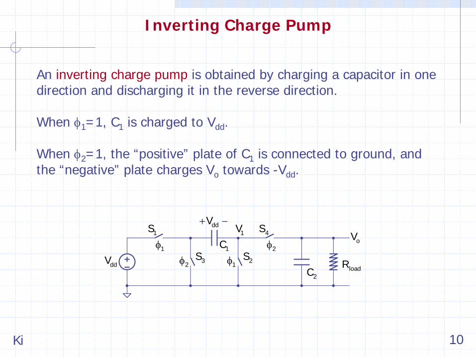
Inverting Charge Pump
1C
loadR2S
1SoV
3S
4Sφ1
φ1φ2
2C
An inverting charge pump is obtained by charging a capacitor in one direction and discharging it in the reverse direction.
When φ1 =1, C1 is charged to Vdd .
When φ2 =1, the “positive” plate of C1 is connected to ground, and the “negative” plate charges Vo towards -Vdd .
+ −ddV
φ2
1V
ddV

Ki 11
Linear Charge Pump
2C 3C 4C1C 5C loadR
oV2V 3V 4V1V 5V2S 3S 4S1S 5S
φ1φ2φ1φ2
ddV
Principle of operation (with ideal switches):φ1 =1, (φ2 =0), C1 is charged to Vdd .φ2 =1, top of C1 (V1 ) is pushed to 2Vdd , charging C2 to 2Vdd .φ1 =1 again, top of C2 (V2 ) pushed to 2Vdd , charging C3 to 3Vdd .Similarly, Vo =V5 is then 5Vdd .
For N flying capacitors, the conversion ratio M = Vo /Vdd is N+1, and a linear charge pump (LQP) is obtained.
Ki 12
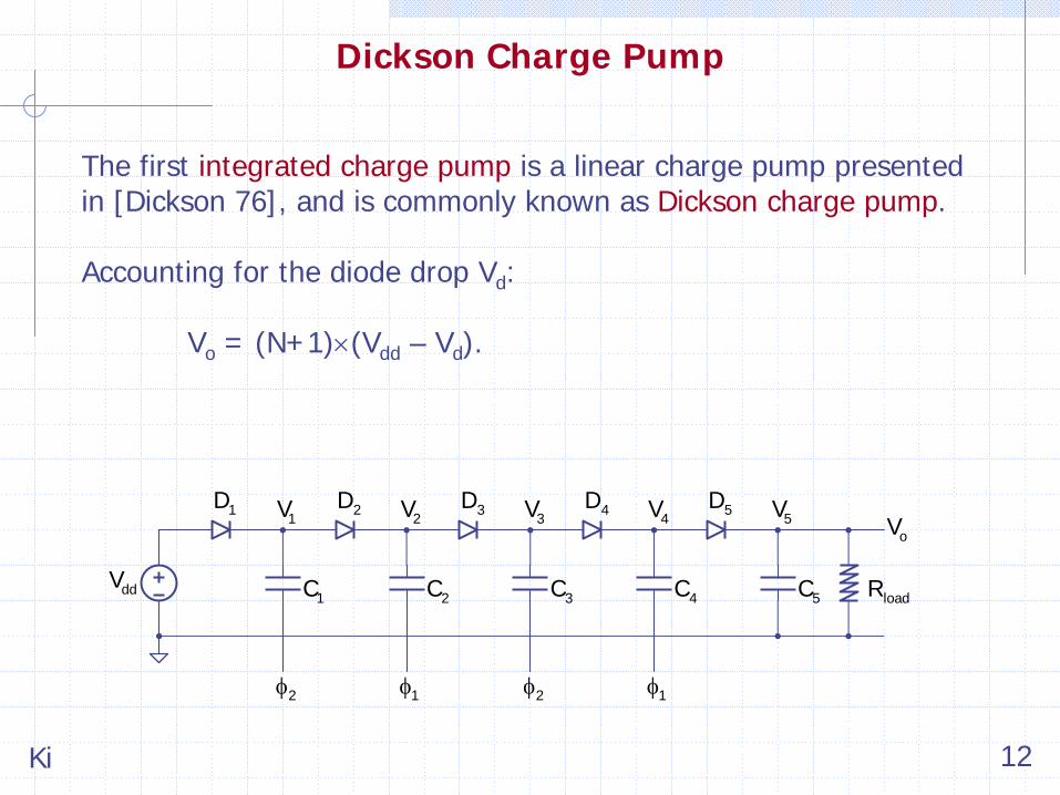
Dickson Charge Pump
The first integrated charge pump is a linear charge pump presented in [Dickson 76], and is commonly known as Dickson charge pump.
Accounting for the diode drop Vd :
Vo = (N+1)×(Vdd – Vd ).
2C 3C 4C1C 5C loadR
oV2V 3V 4V1V 5V2D 3D 4D1D 5D
φ1φ2φ1φ2
ddV

Ki 13
LQP with Diode-Connected Transistors
In [Dickson 76], in fact, diode-connected transistors are used, and
Vo = (N+1)×(Vdd – Vtn(k) ).
For an n-well process, the p substrate (p-sub) has to be connected to GND, and high stage switches Mk (k>1) have body effect, and Vtn(k+1) > Vtn(k) . Eventually, Vtn(k) > Vdd , and adding more stages could not increase the conversion ratio.
2C 3C 4C1C 5C loadR
oV2V 3V 4V1V 5V1M 3M 4M 5M
φ1φ2φ1φ2
ddV
2M
Ki 14
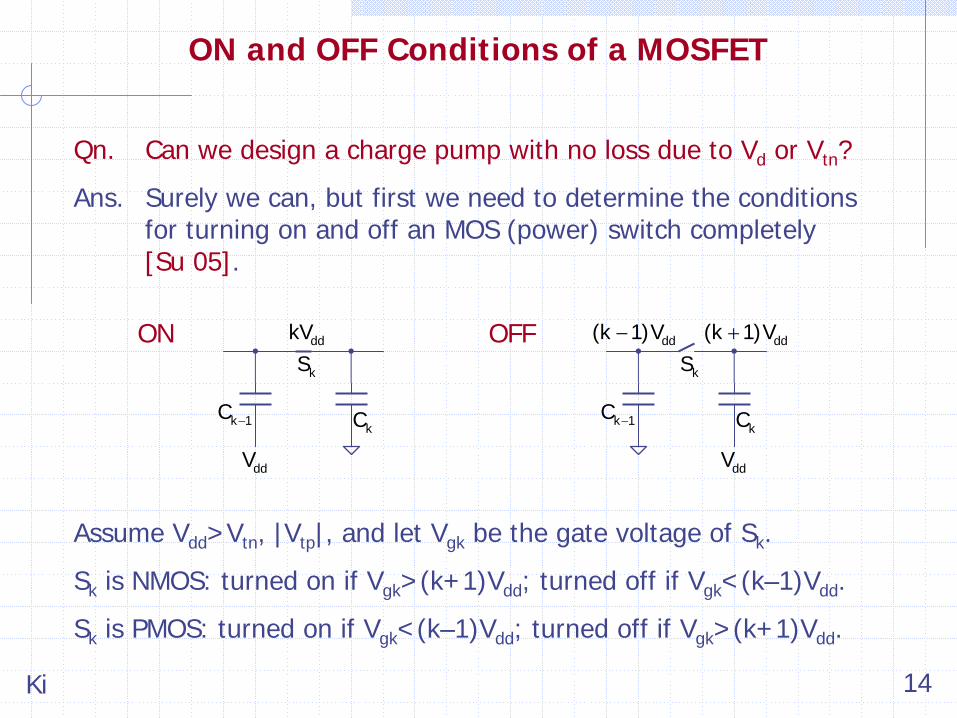
ON and OFF Conditions of a MOSFET
Qn. Can we design a charge pump with no loss due to Vd or Vtn ?
Ans. Surely we can, but first we need to determine the conditions for turning on and off an MOS (power) switch completely [Su 05].
−k 1C
kS
kC
− dd(k 1)V + dd(k 1)V
−k 1C
kS
kC
ddkV
Assume Vdd >Vtn , |Vtp |, and let Vgk be the gate voltage of Sk .
Sk is NMOS: turned on if Vgk >(k+1)Vdd ; turned off if Vgk <(k–1)Vdd .
Sk is PMOS: turned on if Vgk <(k–1)Vdd ; turned off if Vgk >(k+1)Vdd .
ddV ddV
ON OFF

Ki 15
Gate Control Schemes
In [Su 05], a systematic study of gate control for both NMOS and PMOS power switches is presented. For the 5X LQP, S5 has to be PMOS, and gate control circuits for PMOS are shown below.
kM
pkVnkV
HkVLkV
kGC
gkV
First-level gate control: uses a PN pair to control the gate of Mk .
Second-level gate control: treats Mpk (or Mnk ) as Mk , and generates GCpk to drive Mk with a larger gate drive.
nkM pkM
a5M
4V2V
5V
3V
p5GC
g5V
n5M
p5M
4V
3Vb5M
4V
5V
3V
g5V
n5M
p5M

Ki 16
Gate Control Candidates
(VHk , Vpk ) (Vnk , VLk )
GC1 (V1 , φ2 ), (V1 , Vdd ),(V3 , V2 ), (V5 , V4 )
(Vdd , φ1 ), (φ2 , φ1 ), (φ2 , 0)
GC2 (V2 , V1 ), (V4 , V3 ) (V1 , Vdd ), (V1 , φ2 ), (Vdd , φ2 ),(φ1 , φ2 ), (φ1 , 0)
GC3 (V3 , V2 ), (V5 , V4 ) (V2 , V1 ), (Vdd , φ1 ), (φ2 , φ1 ),(φ2 , 0)
GC4 (V4 , V3 ) (V3 , V2 ), (V1 , Vdd ), (V1 , φ2 ),(Vdd , φ2 ), (φ1 , φ2 ), (φ1 , 0)
GC5 (V5 , V4 ) (V4 , V3 ), (V2 , V1 ), (Vdd , φ1 ),(φ2 , φ1 ), (φ2 , 0)

Ki 17
5X LQP w/o Drop Loss
The first LQP that completely eliminates (diode) drop loss is [Cheng 03] using the boldfaced options in the previous page. Only simulation was provided.
Implementation and measurement were finally realized in [Su 05] using the concept of first-level gate control. We labeled it LQP0.
ddV
2V 3V 4V1V1M 3M 4M 5M2M
φ1φ2φ1
φ2
φ2
2C 3C 4C1C 5C loadR
oV5V

Ki 18
ddV
2V 3V 4V1V3M 4M 5M2M
φ1φ2φ1 φ2
2C 3C 4C1C 5C loadR
oV
Improved 5X LQPs
φ2LQP1LQP2
1M
d1MLQP3
The efficiency of LQP0 could be improved by increasing the gate drives of some transistors to 2Vdd :
LQP1: connect VL2 to φ2 so gate drive of M2 is 2VddLQP2: second-level gate control for M5LQP3: change M1 to NMOS, but need Md1 for startup
5V
Ki 19
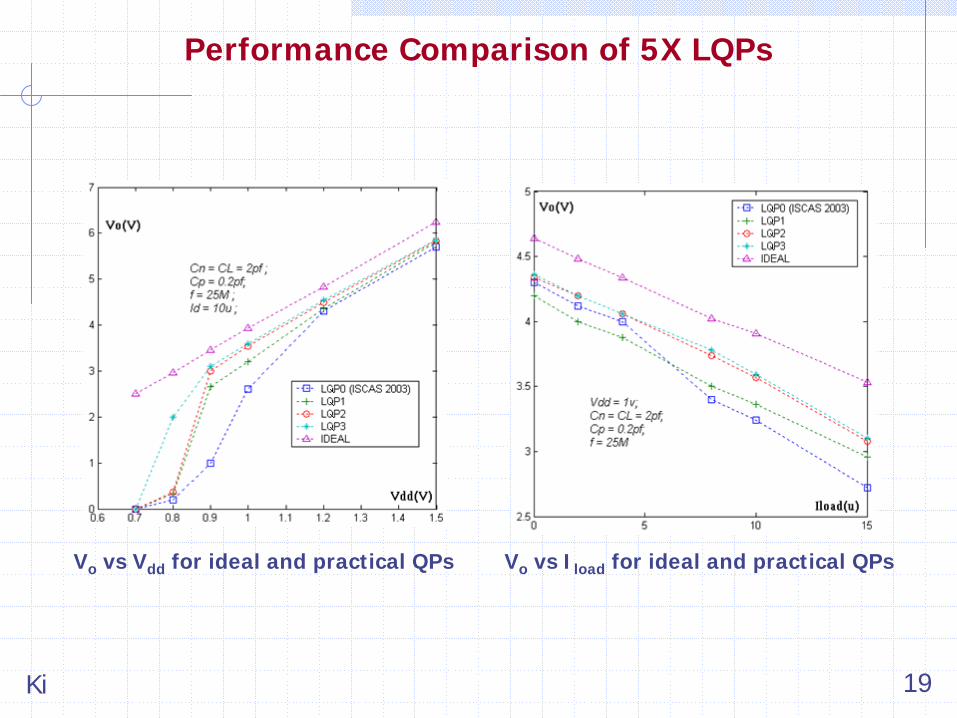
Performance Comparison of 5X LQPs
Vo vs Vdd for ideal and practical QPs Vo vs Iload for ideal and practical QPs

Ki 20
Fibonacci Charge Pump
2C 3C1C
2V 3V1V1aSφ1
φ1
φ2
1cS
1bS
2aS
φ2φ1
φ2
2cS
2bS
3aSφ1
φ1φ2
3cS
3bSoC loadR
oV
ddV
oS
In [Ueno 91], a 2-phase charge pump is suggested that could realize a conversion ratio of 2, 3, 5, 8, 13, etc. that are Fibonacci numbers, and it could be referred as a Fibonacci charge pump (FQP).
In [Makowski 97], it is shown, using graph theoretical concepts, that an FQP achieves the largest conversion ratio using the fewest capacitors among all 2-phase charge pumps.

Ki 21
ANTZ Principle
Qn: How many 2-phase charge pumps could be realized given a specified number of flying capacitors?
Ans: To answer the above question, we need to formulate a systematic construction of charge pumps, the ANTZ principle: All Negative Terminals are connected to Zero (GND) during the charging phase [Su 07].
1C
φc
c1S
p1S c2S
p2S
φcφp
φp
1C
φc
c1S
p1S c2S
p2S
φcφp
φp
Charging Phase Pumping Phase
+−
It should be noted that all published charge pumps are abided by the ANTZ principle, and hence it is not a restrictive requirement.
ANTZ

Ki 22
Charging and Pumping Scenarios
2C 3C 4C1C 5C loadR
oV2V 3V 4V1V 5V2S 3S 4S1S 5S
φ1φ2φ1φ2
ddV
Consider a charge pump structure:
After C4 is charged to 4Vdd in φ2 , it may be connected differently in φ1 :
ddV2C 3C1C
4C 4C 4C 4C
dd5V dd7Vdd5V
dd3VddV dd3V
dd7V
φ2
?
Ki 23
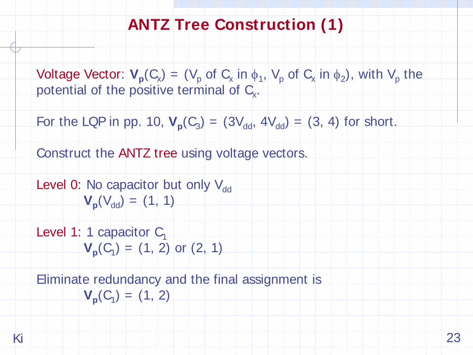
Voltage Vector: Vp (Cx ) = (Vp of Cx in φ1 , Vp of Cx in φ2 ), with Vp the potential of the positive terminal of Cx .
For the LQP in pp. 10, Vp (C3 ) = (3Vdd , 4Vdd ) = (3, 4) for short.
Construct the ANTZ tree using voltage vectors.
Level 0: No capacitor but only VddVp (Vdd ) = (1, 1)
Level 1: 1 capacitor C1Vp (C1 ) = (1, 2) or (2, 1)
Eliminate redundancy and the final assignment isVp (C1 ) = (1, 2)
ANTZ Tree Construction (1)

Ki 24
Level 2: C1 and C2
To avoid redundancy, C2 should not assume (1, 2).
C2 charged in φ1 ⇒
has to be connected in series with C1 and Vdd in φ2 , and gives (1, 3).
C2 charged in φ2 ⇒
(1) charged to Vdd by source and gives (2, 1)(2) charged to 2Vdd by C1 , and gives (3, 2)
Hence, we have the following vector paths (starting from Level 1):(1, 2) →
(1, 3)(1, 2) →
(2, 1)(1, 2) →
(3, 2)
Level 3 and Level 4 are constructed in a similarly fashion.
ANTZ Tree Construction (2)

Ki 25
4-Capacitor ANTZ Tree
(1,5) (2,1)(3,2)(4,3)(5,4)
(2,3) (3,1)(2,4) (3,2)(2,5) (4,2)
(4,3)(5,3)
(3,4) (5,2)(3,5) (4,3)(3,6) (6,3)
(4,5) (5,1)(4,6) (6,2)(4,7) (7,3)
(1,4) (3,2)(2,4) (4,2)(2,5) (4,3)
(5,3)
(1,5) (4,2)(2,6) (5,4)
(6,4)
(1,5) (4,1)(3,5) (5,2)(3,7) (5,4)
(7,4)
(1,6) (4,1)(3,8) (5,2)
(6,5)(8,5)
(4,5) (5,1)(4,6) (5,2)
(6,2)
(5,6) (6,1)(5,7) (7,2)
(1,4) (4,3)(3,2)(2,1) (2,3) (2,4) (3,4) (5,2)(4,1)(3,5)
(1,3) (3,2)(2,1)
(1,2)
(1,1)Level 0
Level 1
Level 2
The 4-capacitor ANTZ tree has 59 configurations.

Ki 26
Charge Pumps from ANTZ Tree
5X Heap Charge Pump [Mihara 95]:(1, 2) →
(1, 3) →
(1, 4) →
(1, 5)
3X Dual-Branch Charge Pump [Pellinconi 03]:(1, 2) →
(2, 1) →
(2, 3) →
(3, 2)
2nX or 2nX (Exponential) Charge Pump (n=2) [Ying 03], [Ki 08]:(1, 2) →
(2, 1) →
(2, 4) →
(4, 2)
5X Linear Charge Pump [Dickson 76]:(1, 2) →
(3, 2) →
(3, 4) →
(5, 4)
8X Fibonacci Charge Pump [Ueno 91]:(1, 2) →
(3, 2) →
(3, 5) →
(8, 5)
New 8X FQP [Su 07]:(1, 2) →
(3, 2) →
(3, 5) →
(3, 8)

Ki 27
Variable Conversion Ratio
Qn: What is the advantage of identifying all possible topologies?
Ans: The ANTZ tree helps to design charge pumps with a variable conversion ratio, by observing that adjacent topologies only differ by one connection.
For example, consider the vector paths:
(1, 2) →
(1, 3) →
(4, 3) →
(4, 5) / (4, 6) / (4, 7)
2C 3C1C
2V 3V1V1aSφ1
φ1
φ2
1cS
1bS
2aSφ2
φ2
2cS
2bS
3aS
φ1φ1 φ2
3cS
3bSoC loadR
oV
ddV
oS4V
φ2φ1
4aSφ1
4bS
φ1 φ2
7X6X5X
4C

Ki 28
Dual-Branch Charge Pumps
Using the same total capacitance, a dual-branch charge pump is more efficient than a single-branch charge pump [Ki 05]:
Cak = Cbk = Ck /2
Hence, dual-branch charge pumps are more suitable for on-chip implementation.
2C1C
φ1φ2
ddVoC loadR
oVφ1 φ2 φ1
a2Ca1C
φ1φ2
ddVoC loadR
oV
φ1 φ2 φ1
b2Cb1C
φ1 φ2
φ1φ2 φ2
Ki 29
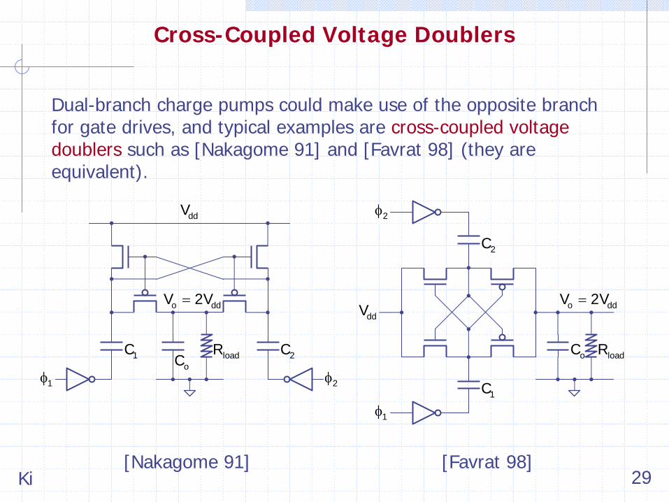
Cross-Coupled Voltage Doublers
Dual-branch charge pumps could make use of the opposite branch for gate drives, and typical examples are cross-coupled voltage doublers such as [Nakagome 91] and [Favrat 98] (they are equivalent).
oC loadR
=o ddV 2VddV
2C
1Cφ1
φ2
oC
=o ddV 2V
φ2
loadR
φ1
1C 2C
ddV
[Nakagome 91] [Favrat 98]

Ki 30
Component-Efficient 2N-X Charge Pumps
A 4X charge pump could be constructed by cascading two 2X cross- coupled doublers, using 16 power switches. [Ying 02] suggests a 4X cross-coupled charge pump using only 14 power switches.
oC
=o ddV 4V
loadR3C 4C
ddV
φ2
2Cφ1
1CddVddV
φ1 φ2

Ki 31
φ1
φ1
φ2
ddVφ4
φ5
φ5
φ6loadR
=o ddV 8Vφ3
φ3
φ4 φ6φ2
φ4
φ6
φ1
φ3
φ5
Qn. Is it possible to design an exponential (2NX) charge pump?
Ans. Yes, [Starzyk 01] suggests a consecutive charging scheme that uses a 2N-phase clock: C1 is charged in φ1 , hold for a long φ2 , within which C2 is charged in φ3 and for a shorter φ4 , but long enough for C3 to charge in φ5 and pump in φ6 .
2N-Phase Exponential Charge Pump
φ2
2C1C
oC
3C
Ki 32
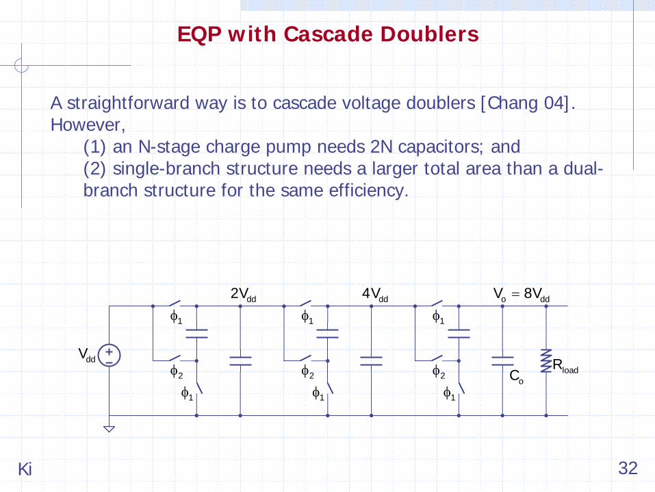
EQP with Cascade Doublers
A straightforward way is to cascade voltage doublers [Chang 04].However,
(1) an N-stage charge pump needs 2N capacitors; and(2) single-branch structure needs a larger total area than a dual- branch structure for the same efficiency.
φ1
φ1
φ2
ddV
dd2V
φ1
φ2
φ1
φ1
φ2loadR
dd4Vφ1
=o ddV 8V
oC
Ki 33
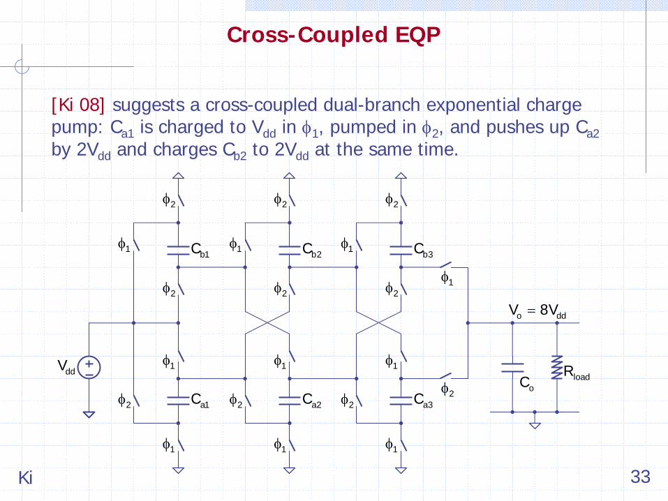
Cross-Coupled EQP
[Ki 08] suggests a cross-coupled dual-branch exponential charge pump: Ca1 is charged to Vdd in φ1 , pumped in φ2 , and pushes up Ca2 by 2Vdd and charges Cb2 to 2Vdd at the same time.
φ1
φ2 a1C
φ1
φ2
φ2
φ1b1C
ddV
φ1
φ2 a2C
φ1
φ2
φ2
φ1b2C
φ1
φ2 a3C
φ1
φ2
φ2
φ1b3C
φ2
φ1
loadR
=o ddV 8V
oC

Ki 34
Properties of Cross-Coupled EQP
Advantages:
(1) Only a 2-phase clock is needed, and gate drive is simpler because dual branch operation provides node voltages to drive the other branch.
(2) Dual branch operation charges the output in both phases, reducing the ripple, or equivalently, enhancing the efficiency as compared to single branch charge pumps.
Disadvantages:
(1) Need 2N capacitors, and may not be good if off-chip capacitors are used.
(2) Using cross-biased nodes for gate drives results in reversion loss.

Ki 35
Multi-Phase Charge Pumps
Qn. Is it possible to design an exponential (2NX) charge pump using only N flying capacitors but using fewer than 2N phases?
Ans. Yes, [Su 08b] suggests a systematic strategy to design multi- phase charge pumps, observing the one voltage criteria.
One voltage criteria: Each capacitor should be charged to only one voltage value that is a multiple of Vdd for all charging phases, and in the discharging phases, the lowering of the capacitor voltage is mainly due to the load current.
With the one voltage criteria, we demonstrate that a 2NX charge pump could be realized using N flying capacitors and only N+1 phases.

Ki 36
1C 2C 3C LC
1X1C
2C 3C LC1C
2C
3C LC
2X2X 4X
2X
4X
4X
4X5X2X 5X 5X
4X
1C
2C
3C LC
2X
4X
1X
1C
2C 3C LC
5X
2X4X
1C 2C 3C LC
1X1C
2C 3C LC
2X
4X 4X6X2X1C
2C
3C LC
2X
4X
1C2C
3C LC
2X
4X
1C 2C 3C LC
1X1C
2C 3C LC
2X
6X 6X
6X
4X 4X7X2X1C
2C
3C LC
2X
4X
1C
2C
3C LC
5X
4X
1C 2C 3C LC
1X1C
2C 3C LC
2X
7X
7X7X 1X
1φ 2φ 3φ 4φM
(a)4
5
6
7
3/4-Phase QPs with 3 Flying Capacitors

Ki 37
4X
7X
3X
1C
2C
3C
LC
2X
1C
2C
3C LC
1X1C
2C 3C LC
2X
7X
7X3X
4X 4X2X1C
2C
3C LC
2X
4X
1C 2C 3C LC
1X1C
2C 3C LC
2X 4X
1C
2C
3C
LC
2X
8X
(b)
(c)
7
8
Multi-Phase 7X and 8X Charge Pumps
8X 8X 8X
Ki 38
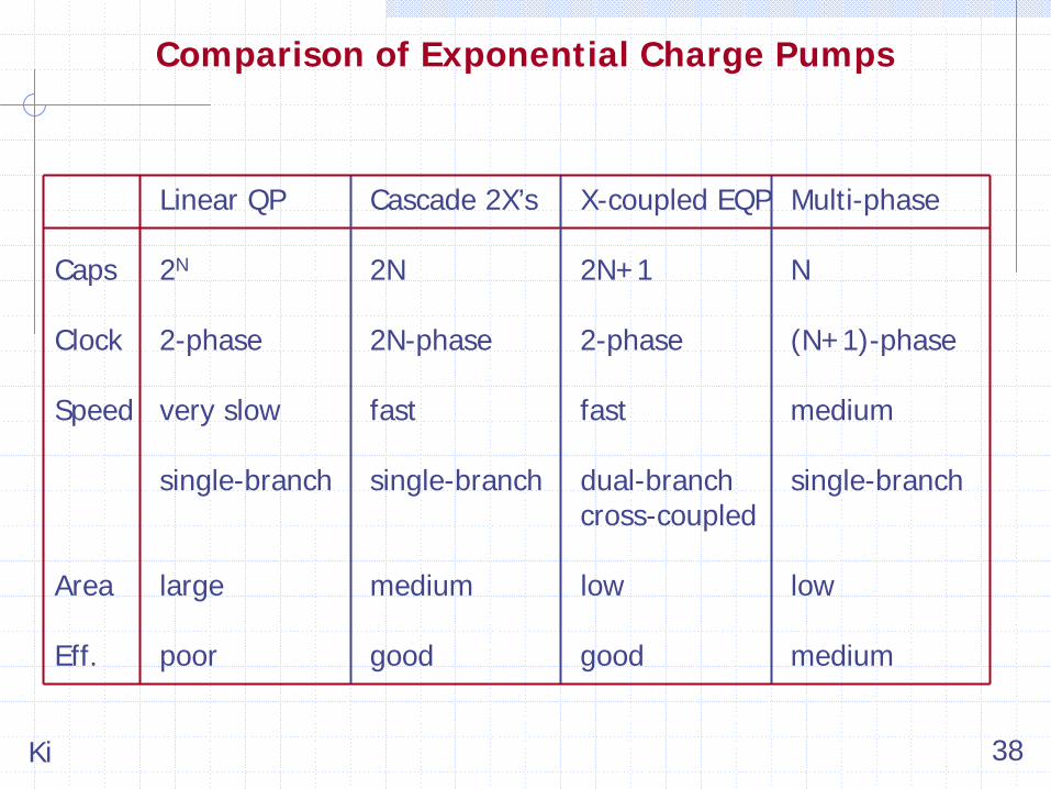
Comparison of Exponential Charge Pumps
Linear QP Cascade 2X’s X-coupled EQP Multi-phase
Caps 2N 2N 2N+1 N
Clock 2-phase 2N-phase 2-phase (N+1)-phase
Speed very slow fast fast medium
single-branch single-branch dual-branch single-branchcross-coupled
Area large medium low low
Eff. poor good good medium

Ki 39
Voltage Doubler + LDR
To achieve a regulated output voltage, a straightforward method is to cascade the charge pump with a low dropout regulator (LDR) to achieve a regulated charge pump (RQP).
dd2V
refV loadR
ddV
aC
φ1
φ2
φ1
φ1
φ2φ2 LDRM
a2Ma1M
a3M a4M
bCb2M
b1M
b3M b4M
oCmC
oV
EA

Ki 40
RQP with Quasi Switches
In [Chung 98], the switches Ma4 and Mb4 are turned into controlled current sources (resistors), coined quasi switches, and charges Ca and Cb to V1 ([Chung 98] uses only single-branch) such that
Vo = Vdd + V1
refV loadR
ddV
aC
φ1
φ2
φ1
φ1
φ2φ2
a2Ma1M
a3M a4M
bCb2M
b1M
b3M b4M
oC
oV
φ1
φ2
φ1
φ2
EA

Ki 41
Switching Low Dropout Regulator
The RQP with quasi-switches cannot achieve in-phase regulation, and the best is to combine Ma2 (Mb2 ) with MLDR , and the scheme is coined switching low dropout regulator (SLDR) [Chen 01].
refV loadR
ddV
aC
φ1
φ2
φ1
φ1
φ2φ2
a2Ma1M
a3M a4M
bCb2M
b1M
b3M b4M
oC
oVφ1 φ2
EA

Ki 42
RQP with Pseudo-Continuous Regulation
An alternative way to achieve in-phase regulation is to incorporate MLDR into Ma3 (Mb3 ), and the scheme is coined pseudo-continuous regulation [Lee 05].
ddV
aC
φ1
φ2
φ1
φ1
φ2φ2
a2Ma1M
a3M a4M
bCb2M
b1M
b3M b4M
refV loadRoC
oV
φ1
φ2
φ1
φ2
EA

Ki 43
aC bC
ddVddV
φ1 a1M
φ1
φ2
φ2
φ2
a1D
φ1
a1V
dd2V
a2V b2V
b1V
oV
dd2V
b2D
b1D
a2D
oC
obVrefV
a2M b2M
b1M
RQP with Active Diodes
An alternative way of implementing the switching LDR is to use active diodes, i. e., using MOS transistors with control to replace the diodes [Lam 06a].
EAeaV

Ki 44
dd2V
a1D
ddV
ddV
a1V
aC
a2V
level shifter
4T voltagecomparator
Na1M
Pa1M
GaV
a2to D
biasI
Implementation of Da1
An active diode is an MOS switch with a differential common gate comparator and level shifter [Lam 06a].
biasV
Ki 45
01a1V
aC
a2V
biasV
eaV
dd2V
Pa3M
Pa2M
dd2V
a2D
oV
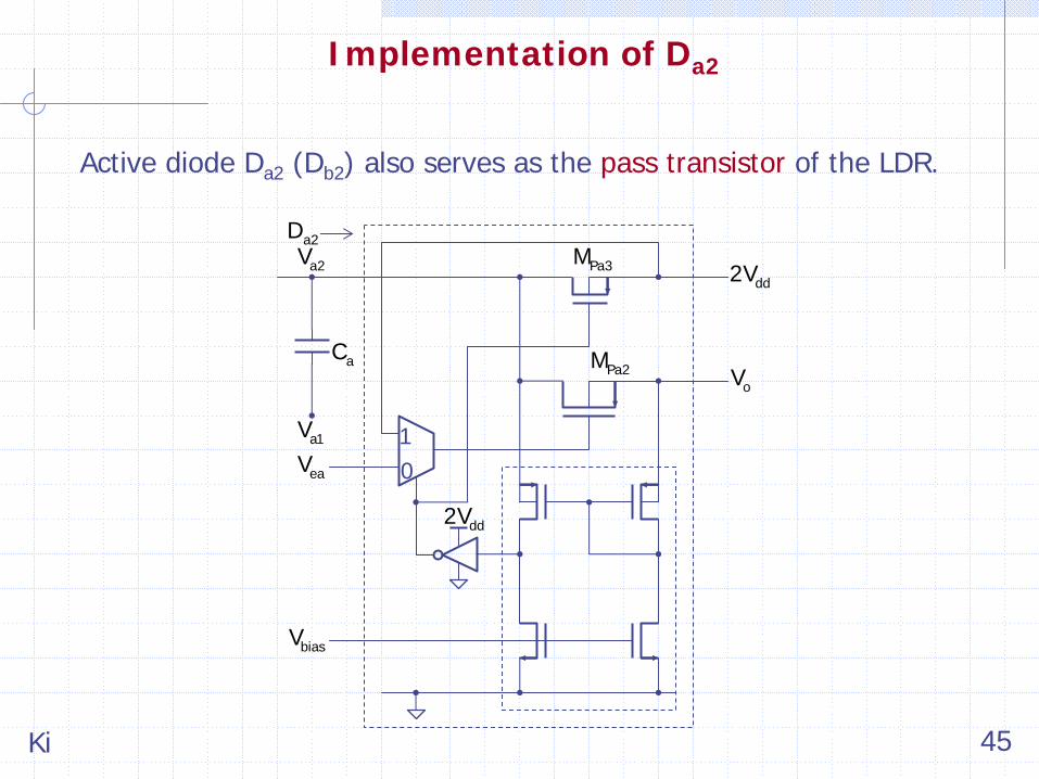
Implementation of Da2
Active diode Da2 (Db2 ) also serves as the pass transistor of the LDR.

Ki 46
RQP with Continuous Output Regulation (1)
To achieve (in-phase) continuous output regulation, a 4-phase clock with interleaving control is proposed [Su 09].
a1 a1S ( )φ
aVbV
a3 a 2S ( )φ
a2 a2S ( )φ
a4 a1S ( )φ
aC
bCb3 b2S ( )φ
b1 b1S ( )φ b2 b2S ( )φ
b4 b1S ( )φ
LCddV
inI chIoV
bV
aV
inIchIoV
ivt
a1φ
a 2φ
b1φ
b2φ
Branch A
Branch B
Voltage doubler with 4-phase interleaving clock:

Ki 47
aC
b C− +
a1 a2
b1 b2
( , ) (1,0)( , ) (0,1)φ φ =φ φ =
aC
b C− +
(0,0)(0,1)
b C− +
(0,1)(0,1)
a C− +
bC
(0,1)(0,0)
a C− +
bC
(0,1)(1,0)
a C− +bC
(0,1)(0,0)
a C− +
b C− +
(0,1)(0,1)
a C− +
aC
b C− +
(0,0)(0,1)
iv
interleavingsessions (t )
RQP with Continuous Output Regulation (2)
The interleaving scenario:

Ki 48
RQP with Continuous Output Regulation (3)
The LDR architecture:
b2φ
a 2φ
b1φ
a1φa 2g
aV
bVb1M
a 2M
b2M
a1M
buffer
ctrlV
oV
a 2φ a1φ
b1φb2φ
ddVobV
refV
maxV
a3M a 4M
b3M b4M
ahM
bhM
faC
fbC
buffer
buffer buffer
amV
bmV
a1g
b1g
ahg
bhgb2g
feedbackcontroller
1R
2RLC LR
HC
GD A1 GD A2
GD B1 GD B2

Ki 49
Remarks
A systematic study of charge pumps should cover analysis, topology, gate control and regulation. This talk only covers snapshots on topology, gate control and regulation.
The talk centered on the research activities at HKUST. The attached reference section only mentions those papers (in chronological order) that are directly useful for the discussion:
[BLUE] Papers from other institutions[RED] HKUST papers (Ki’s research group)[PINK] HKUST papers (Mok’s and Tsui’s research groups)
The reference section tabulates all publications since the setup of the Integrated Power Electronics Lab. in 1995 up to Sept. 2009, and topics such as analysis, AC-DC charge pumps, energy harvesting applications, etc., are not covered in this talk due to limited time.
Ki 50
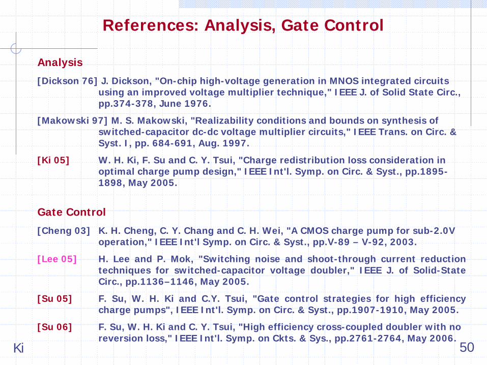
References: Analysis, Gate Control
Analysis
[Dickson 76] J. Dickson, "On-chip high-voltage generation in MNOS integrated circuits using an improved voltage multiplier technique," IEEE J. of Solid State Circ., pp.374-378, June 1976.
[Makowski 97] M. S. Makowski, "Realizability conditions and bounds on synthesis of switched-capacitor dc-dc voltage multiplier circuits," IEEE Trans. on Circ. & Syst. I, pp. 684-691, Aug. 1997.
[Ki 05] W. H. Ki, F. Su and C. Y. Tsui, "Charge redistribution loss consideration in optimal charge pump design," IEEE Int'l. Symp. on Circ. & Syst., pp.1895- 1898, May 2005.
Gate Control
[Cheng 03] K. H. Cheng, C. Y. Chang and C. H. Wei, "A CMOS charge pump for sub-2.0V operation," IEEE Int'l Symp. on Circ. & Syst., pp.V-89 – V-92, 2003.
[Lee 05] H. Lee and P. Mok, "Switching noise and shoot-through current reduction techniques for switched-capacitor voltage doubler," IEEE J. of Solid-State Circ., pp.1136–1146, May 2005.
[Su 05] F. Su, W. H. Ki and C.Y. Tsui, "Gate control strategies for high efficiency charge pumps", IEEE Int'l. Symp. on Circ. & Syst., pp.1907-1910, May 2005.
[Su 06] F. Su, W. H. Ki and C. Y. Tsui, "High efficiency cross-coupled doubler with no reversion loss," IEEE Int'l. Symp. on Ckts. & Sys., pp.2761-2764, May 2006.

Ki 51
References: Topology (1)
[Dickson 76] J. Dickson, "On-chip high-voltage generation in MNOS integrated circuits using an improved voltage multiplier technique," IEEE J. of Solid State Circ., pp.374-378, June 1976.
[Nakagome 91] Y. Nakagome et al., "An experimental 1.5-V 64-Mb DRAM," IEEE J. of Solid-States Circ., pp. 465-472, March 1991.
[Ueno 91] F. Ueno et. al., "Emergency power supply for small computer systems," IEEE Int. Symp. Circ. & Syst.., 1991, pp. 1065–1068.
[Mihara 95] M. Mihara, Y. Terada and M. Yamada, "Negative heap pump for low voltage operation flash memory," IEEE VLSI Symp. on Circ., 1995, pp. 75–76.
[Favrat 98] P. Favrat, P. Deval and M. J. Declercq, "A high efficiency CMOS voltage doubler," IEEE J. of Solid-States Circ., March 1998, pp.410-416.
[Starzyk 01] J. A. Starzyk, Y. W. Jan and F. Qiu, “A DC-DC charge pump design based on voltage doublers,” IEEE Trans. on Circ. & Syst., pp.350-359, March 2001.
[Ying 02] T. R. Ying, W. H. Ki and M. Chan, "Area-efficient CMOS integrated charge pumps," IEEE Int'l. Symp. on Circ. & Syst., Scottsdale, USA, pp.III.831- III.834, May, 2002.
[Cheng 03] K. H. Cheng, C. Y. Chang and C. H. Wei, "A CMOS charge pump for sub-2.0V operation," IEEE Int'l Symp. on Circ. & Syst., pp.V-89 – V-92, 2003.

Ki 52
References: Topology (2)
[Pelliconi 03] R. Pelliconi et. al., "Power efficient charge pump in deep submicron standard CMOS technology," IEEE J. Solid-State Circ., pp. 1068–1071, Jun. 2003.
[Ying 03] T. R. Ying, W. H. Ki and M. Chan, "Area-efficient CMOS charge pumps for LCD drivers," IEEE J. of Solid-State Circ., pp.1721-1725, Oct. 2003.
[Chang 04] L. K. Chang and C. H. Hu, “An exponential-folds design of a charge pump styled DC/DC converter,” IEEE Power Elec. Specialists Conf., pp.516-520, June 2004.
[Ki 05] W. H. Ki, F. Su and C. Y. Tsui, "Charge redistribution loss consideration in optimal charge pump design," IEEE Int'l. Symp. on Circ. & Syst., pp.1895- 1898, May 2005.
[Su 07] F. Su and W. H. Ki, "Design strategy for step-up charge pumps with variable integer conversion ratios," IEEE Trans. on Circ. & Syst. II, pp.417-421, May 2007.
[Ki 08] W. H. Ki, F. Su, Y. H. Lam and C. Y. Tsui, "N-stage exponential charge pumps, charging stages therefor and methods of operation therefor," US Patent 7,397,299, July 8, 2008.
[Su 08c] F. Su and W. H. Ki, "An integrated reconfigurable SC power converter with hybrid gate control scheme for mobile display driver applications," IEEE Asian Solid-State Circ. Conf., pp.169-172, Nov. 2008.

Ki 53
References: Regulated Charge Pumps
[Chung 98] H. Chung, "Design and analysis of quasi-switched-capacitor step-up DC/DC converter," IEEE Int'l. Symp. on Circ. & Syst., pp.IV-438 – IV-441, 1998.
[Chen 01] W. Chen, W. H. Ki, P. Mok and M. Chan, "Switched-capacitor power converters with integrated low dropout regulators," IEEE Int'l. Symp. on Circ. & Syst., pp.III-293 - III-296, May 2001.
[Chan 02] C. S. Chan, W. H. Ki and C. Y. Tsui, "Bi-directional integrated charge pumps," IEEE Int'l. Symp. on Circ. & Syst., pp.III.827-III.830, May, 2002.
[Lee 05] H. Lee and P. Mok, “A SC DC-DC converter with pseudo-continuous output regulation using a three-stage switchable opamp,” IEEE Int’l Solid-State Circ. Conf., pp.288-289+599, Feb. 2005.
[Lam 06a] Y. H. Lam, W. H. Ki and C. Y. Tsui, "An integrated 1.8V to 3.3V regulated voltage doubler using active diodes and dual-loop voltage follower for switch-capacitive load," IEEE VLSI Symp. on Tech. & Circ., pp.104-105, June 2006.
[Lee 07] H. Lee and P. Mok, "An SC voltage doubler with pseudo-continuous output regulation using a three-stage switchable opamp," IEEE J. of Solid-State Circ., pp. 1216-1229, June 2007.
[Su 08a] F. Su, W. H. Ki and C. Y. Tsui, "An SC voltage regulator with novel area- efficient continuous output regulation by a dual-branch interleaving control scheme," IEEE VLSI Symp. on Tech. & Circ., pp.136-137, June, 2008.
[Su 09] F. Su and W. H. Ki, "Regulated switched-capacitor doubler with interleaving control for continuous output regulation," IEEE J. of Solid-State Circ., pp. 1112-1120, Apr. 2009.

Ki 54
References: M-Phase, AC-DC, Energy Harvesting QPs
Multi-Phase Charge Pumps
[Su 08b] F. Su and W. H. Ki, "Component-efficient multi-phase switched capacitor DC-DC converter with configurable conversion ratios for LCD driver applications," IEEE Trans. on Circ. & Syst. II, pp.753-757, Aug. 2008.
AC-DC Charge Pumps
[Lam 06b] Y. H. Lam, W. H. Ki and C. Y. Tsui, "Integrated low-loss CMOS active rectifier for wirelessly powered devices," IEEE Trans. on Circ. & Syst. II, pp.1378-1382, Dec. 2006.
[Yi 07] J. Yi, W. H. Ki and C. Y. Tsui, "Analysis and design strategy of UHF micro- power CMOS rectifiers for micro-sensor and RFID applications," IEEE Trans. on Circ. & Syst. I, pp.153-166, Jan. 2007.
Energy Harvesting Charge Pumps
[Tsui 05] C. Y. Tsui, H. Shao, W. H. Ki and F. Su, "Ultra-low voltage power management and computation methodology for energy harvesting applications," IEEE VLSI Symp. on Tech. & Circ., pp.316-319, June 2005.
[Tsui 06] C. Y. Tsui, H. Shao, W. H. Ki and F. Su, "Ultra-low voltage power management and computation methodology for energy harvesting applications," Asia South Pacific Design Automation Conf., LSI University Design Contest, pp.96-97, Jan. 2006.

Ki 55
References: Charge Pumps for Energy Harvesting
[Shao 06] H. Shao, C. Y. Tsui and W. H. Ki, "A novel charge based computation system and control strategy for energy harvesting applications," IEEE Int'l. Symp. on Circ. & Syst., pp.2933-2936, May 2006.
[Shao 07a] H. Shao, C. Y. Tsui and W. H. Ki, "An inductor-less micro solar power management system design for energy harvesting applications," IEEE Int'l. Symp. on Circ. & Syst., pp.1353-1356, May 2007.
[Shao 07b] H. Shao, C. Y. Tsui and W. H. Ki, "A micro power management system and maximum output power control for solar energy harvesting applications", IEEE Int'l Symp. on Low Power Elec. Devices, pp.298-303, Aug. 2007.
[Yi 08] J. Yi, F. Su, Y. H. Lam, W. H. Ki and C. Y. Tsui, "An energy-adaptive MPPT power management unit for micro-power vibration energy harvesting," IEEE Int'l. Symp. on Circ. & Syst., May 2008, pp.2570-2573.
[Shao 09a] H. Shao, C. Y. Tsui and W. H. Ki, "An inductor-less MPPT design for light energy harvesting systems," Asia South Pacific Design Automation Conf., LSI University Design Contest, pp.101-102, Jan. 2009.
[Shao 09b] H. Shao, C. Y. Tsui and W. H. Ki, "The design of a micro power management system for applications using photovoltaic cells with the maximum output power control," IEEE Trans. on VLSI Syst., pp.1138- 1142, Aug. 2009.

Ki 56
BLANK

IC Design ofPower Management Circuits (VI)
Wing-Hung KiIntegrated Power Electronics Laboratory
ECE Dept., HKUSTClear Water Bay, Hong Kong
www.ee.ust.hk/~eeki
International Symposium on Integrated CircuitsSingapore, Dec. 14, 2009

2
Part VI
Introduction toLow Dropout Regulators

3
Content
Generic Linear Regulator
Low Dropout Regulator
Simple Low Dropout Regulator

4
Generic Linear Regulator
C LR
oV
1R
2R
obV
VREF
NM
EAddV
Q1I oIQ3IQ2I
ddI
Linear Regulator
A linear regulator consists of a pass transistor inserted between the input supply voltage Vdd and the required output voltage Vo , and a feedback circuit for controlling the voltage drop across the pass transistor such that Vo is kept constant. In CMOS design, the pass transistor could be an NMOS or a PMOS transistor.

5
Dropout Voltage of Linear Regulator
One important parameter of a linear regulator is the dropout voltage (VDO ) that is defined as the minimum voltage difference between Vdd and Vo such that the regulator still performs satisfactorily as a linear regulator:
VDO = min[Vdd – Vo ]
As Vo is usually fixed, we have
VDO = Vddmin – Vo
For the linear regulator in the previous page, the high output swing of the error amplifier EA is Vdd –Vov , and VgsN = Vtn +Vov (Vov is the gate overdrive voltage of all transistors), and Vddmin is computed as
Vddmin = Vo + VgsN + Vov
= Vo + Vtn + 2Vov
6
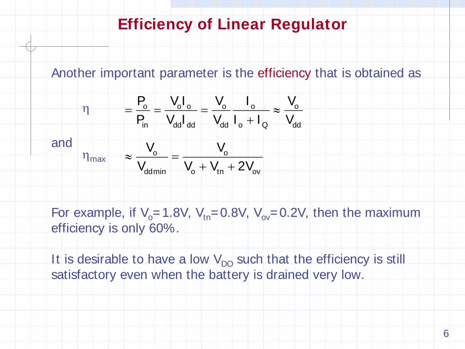
Efficiency of Linear Regulator
Another important parameter is the efficiency that is obtained as
= = = ≈+
o o o o o o
in dd dd dd o Q dd
P V I V I VP V I V I I V
For example, if Vo =1.8V, Vtn =0.8V, Vov =0.2V, then the maximum efficiency is only 60%.
It is desirable to have a low VDO such that the efficiency is still satisfactory even when the battery is drained very low.
η
andηmax ≈ =
+ +o o
ddmin o tn ov
V VV V V 2V

7
Low Dropout Regulator
C LR
oV
1R
2R
obV
VREF
PM
EAddV
Q1I oIQ3IQ2I
ddI
Low Dropout Regulator
Low dropout regulators (LDRs) could be achieved by using a higher supply voltage for EA through using an on-chip charge pump. Yet, a popular method is to use a PMOS pass transistor, (V+ and V– have to be swapped), and Vddmin = Vo +Vov , giving
ηmax ≈ =+
o o
ddmin o ov
V VV V V
(ηmax = 90% with the previous parameters)
8
Simple Low Dropout Regulator
1M 2M
3M4M
LC
PC
PM
1R
2RobV
ESRRoV
aV
LR
ddV
0MbnV
refV
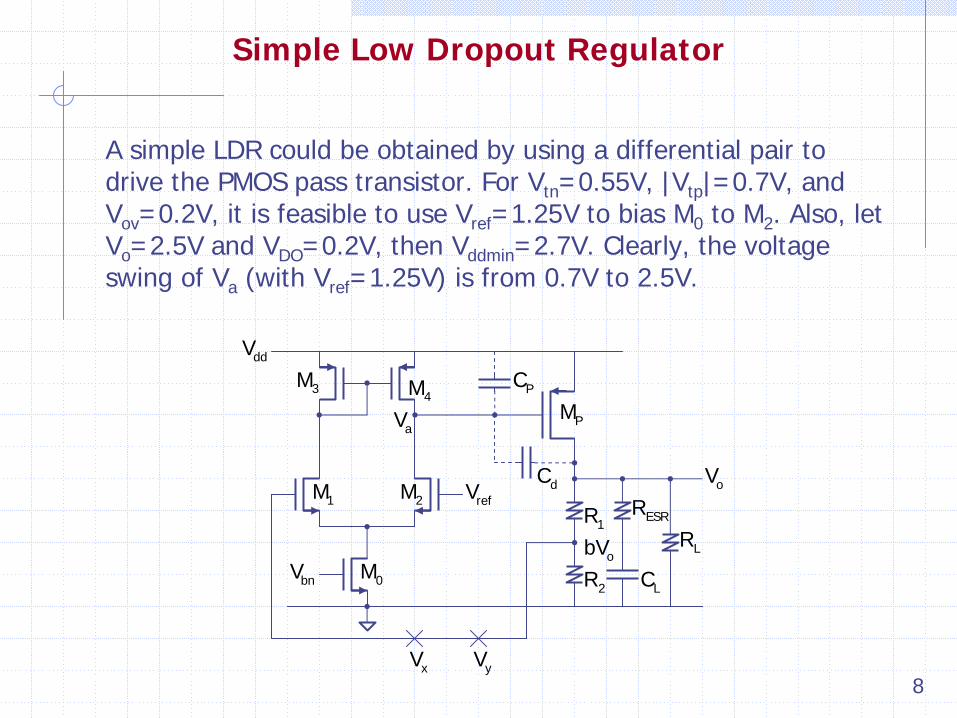
A simple LDR could be obtained by using a differential pair to drive the PMOS pass transistor. For Vtn =0.55V, |Vtp |=0.7V, and Vov =0.2V, it is feasible to use Vref =1.25V to bias M0 to M2 . Also, let Vo =2.5V and VDO =0.2V, then Vddmin =2.7V. Clearly, the voltage swing of Va (with Vref =1.25V) is from 0.7V to 2.5V.
xV yV
dC

9
Complications in LDR Analysis
Although the simple LDR resembles a 2-stage amplifier of which the analysis is well-known, there are complications.
1. In many analyses, only the gate capacitance of the pass transistor CgP (=CP ) is considered; but in fact the gate-drain overlap capacitance CgdoP (=Cd ) is quite large and should not be omitted.
2. The output current could change by 5 orders of magnitudes (say, from 10μA to 100mA), and the pass transistor will transit from the sub-threshold region to the active region.
3. For aggressive design in using a smaller pass transistor, it will operate in the triode region at high currents.
4. Both CP and Cd depends on the load current.
10
Simple LDR: Small Signal Model
T(s)
oT = ma mp a obg g R R
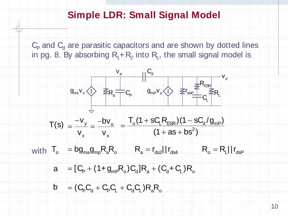
CP and Cd are parasitic capacitors and are shown by dotted lines in pg. 8. By absorbing R1 +R2 into RL , the small signal model is
− −= =y o
x x
v bvv v
with
m1 xg vPC
dCav
aR dsPrmP ag vLR
LC
ESRRov
+ −=
+ +o L ESR d mP
2
T (1 sC R )(1 sC /g )(1 as bs )
a = + +P mP o d a d L o[C (1+g R )C ]R (C +C )R
b = + +P d P L d L a o(C C C C C C )R R
=o L dsPR R ||r=a ds2 ds4R r ||r

11
+=
+ +o ESR
o a
T (1 s/z )(1 s/p )(1 s/p )
Simple LDR: Loop Gain Function
Note that CL >>>CP , Cd , we have
a ≈
CL Ro = CL (RL ||rdsP )
b ≈
(CP +Cd )CL Ra Ro
and gmP /Cd >> zESR , then the loop gain function is given by
T(s)
oT = ma mp ds2 ds4 L dsPbg g (r || r )(R || r )with
ESRz =L ESR
1C R
op =L L dsP
1C (R || r )
ap =+P d ds2 ds4
1(C C )(r || r )

12
Simple LDR: Numerical Example
The simple LDR is designed using a 0.35μm CMOS process:
μn Cox =110μA/V2, μp Cox =35μA/V2, Vtn =0.55V, |Vtp |=0.7V, λn =0.1/V@L=0.5μm, |λp |=0.1/V@L=1μm
Vdd =2.7V, Vo =2.5V, Vref =1.25V, b=0.5, CL =10μF, I1,2 =50μA, Iomax =100mA
At Io =Iomax , MP is at the edge of active region, and× μ
= =μμ × 2
2 100m 50,000 m0.35 m35 0.2
⎛ ⎞⎜ ⎟⎝ ⎠P
WL
The gate capacitance CP and gate-drain overlap capacitance CgdoP (=Cd ) depends on the load current Io :
Io CP Cd0.1mA 9.5pF 10pF1mA 12.5pF 10pF10mA 50pF 13pF100mA 50pF 13pF

13
Simple LDR: Diff Pair Parameters
m1,2g × μ= = μ
2 50 500 A/V0.2
ds2,4r = = Ω× μ1
200k0.1 50
Consider the pass transistor to operate at Iomax =100mA first.To achieve λn =|λp |=0.1/V, Ln =0.5μm, and Lp =1μm, and
× μ μ= ≈
μμ × 2
2 50 12 m0.5 m110 0.2
⎛ ⎞⎜ ⎟⎝ ⎠1,2
WL
⎛ ⎞⎜ ⎟⎝ ⎠3,4
WL
μ⎛ ⎞= ≈⎜ ⎟ μ⎝ ⎠1,2
W 67.5 m3L 1 m
ap = =×1
160k rad/s63p 100k
1A = μ × =500 100k 50 V/V (34dB)
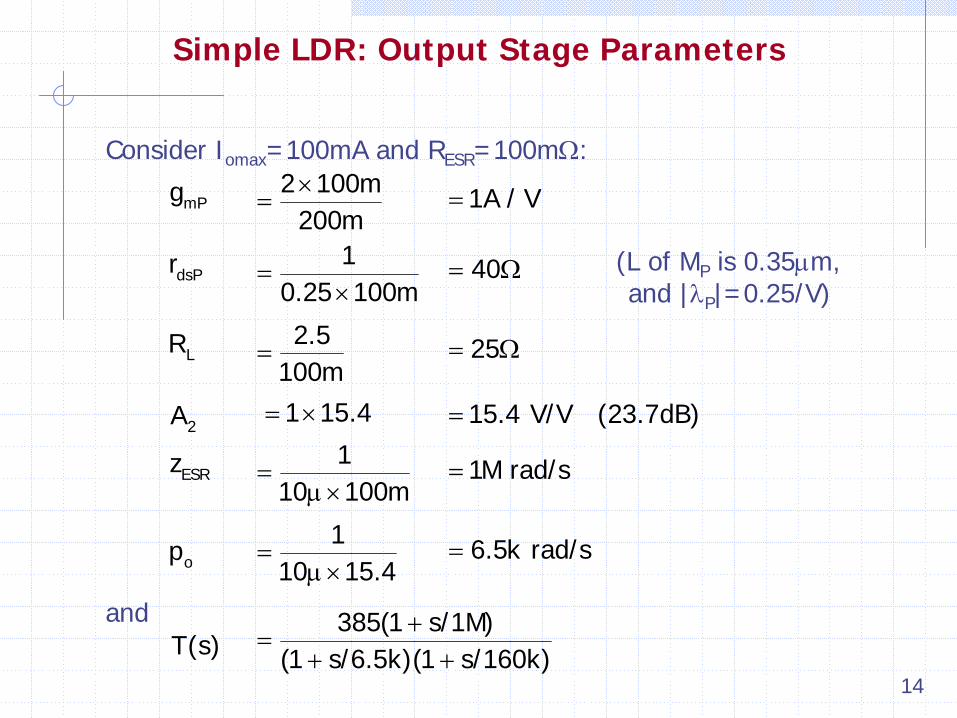
14
mPg ×=
2 100m200m
dsPr =×1
0.25 100m
Simple LDR: Output Stage Parameters
LR =2.5
100m
2A = ×1 15.4
op =μ ×
110 15.4
Consider Iomax =100mA and RESR =100mΩ:
and +=
+ +385(1 s/1M)
(1 s/6.5k)(1 s/160k)T(s)
=μ ×
110 100m
ESRz
= 1A / V
= Ω40
= Ω25
= 15.4 V/V (23.7dB)
= 1M rad/s
= 6.5k rad/s
(L of MP is 0.35μm, and |λP |=0.25/V)

15
Simple LDR: T(s) at Lower Currents
The output stage is affected by Io . Let Io =f×Iomax , and
mPg ' = μ =o p ox P mP2I C (W/L) f×g
oR ' = =L dsP o(R '||r ') R /f
T '(s)+
=+ +
o ESR
o a
(T / f )(1 s/z )[1 s/(f×p )](1 s/p )
The loop gain function is then given by
++ +
385(1 s/1M)(1 s/6.5k)(1 s/160k)
1mA
++ +
1217(1 s/1M)(1 s/650)(1 s/160k)
++ +3850(1 s/1M)
(1 s/65)(1 s/160k)
Io T(s)
10mA
100mA

16
100 10M
1M
100k10k1k 100M
60dB
40dB
20dB
10
− o90
− o180
0dB
o0100mA
1mA
1mA 10mA
10mA100mA
|T|
/T
Simple LDR: Bode Plots of T(s)
160k

17
Simple LDR: Computation vs Simulation
Io To UGF φm
1mA* 71.5dB 32kHz 55o
10mA 61.5dB 57kHz 55o
100mA 51.5dB 100kHz 55o
Computation:
Io To UGF φm
1mA* 57.1dB 13kHz 70o
10mA 56.2dB 46kHz 40o
100mA 45.8dB 94kHz 42o
Simulation:
* At 1mA MP is in sub-threshold and resulted in large discrepancy.

18
Simple LDR: Remarks
(1) To maintain stability, a relatively large output capacitor CL is used.
(2) A relatively large ESR (100mΩ) is needed to achieve a marginal phase margin (around 45o).
(3) The gate-drain overlap capacitance Cd is miller multiplied by the gain of the output stage, but the gain is too low to affect the dominant pole po . However, the pole pa should be modified to 1/(CP +Cd )Ra for better accuracy.
(4) For low output current, the pass transistor enters sub- threshold region. A more accurate small signal model should take this into account.
Related Documents


