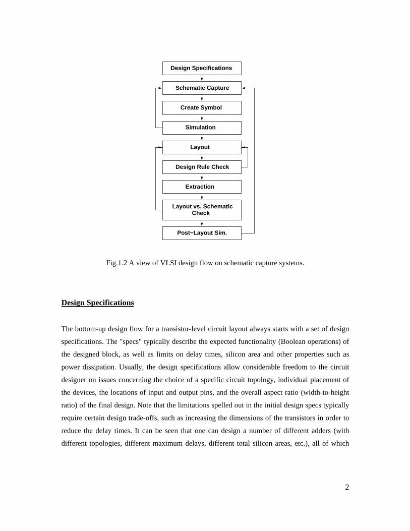
1 1.2 IC Design Flow The IC design process starts with a given set of requirements. After the development, this initial design is tested against the initial design requirements. When these requirements are not satisfied, the design must be improved. If such improvement is either not possible or too costly, then the requirements must be revised and the IC design process re-starts with the new modified requirements. The failure to properly verify a design in its early phases typically causes significant and expensive re-design at a later stage, which ultimately increases the time-to- market. Thus, the verification of the design plays a very important role in every step. Fig.1.2 provides a view of the Very large scale integration (VLSI) design flow based on schematic capture systems. Although the design process has been described in a linear fashion for simplicity, in reality there are many iterations back and forth, especially between any two neighboring steps, and occasionally even remotely separated pairs. Although top-down design flow provides an excellent design process control, in reality, there is no truly unidirectional top- down design flow. Both top-down and bottom-up approaches have to be combined. For instance, if a chip designer defined an architecture without close estimation of the corresponding chip area, then it is very likely that the resulting chip layout will exceed the area limit of the available technology. In such a case, in order to fit the architecture into the allowable chip area, some functions may have to be removed and the design process must be repeated. Such changes may require significant modification of the initial requirements. Thus, it is very important to feed forward low-level information to higher levels (bottom up) as early as possible.

Welcome message from author
This document is posted to help you gain knowledge. Please leave a comment to let me know what you think about it! Share it to your friends and learn new things together.
Transcript
1
1.2 IC Design Flow
The IC design process starts with a given set of requirements. After the development, this initial
design is tested against the initial design requirements. When these requirements are not satisfied,
the design must be improved. If such improvement is either not possible or too costly, then the
requirements must be revised and the IC design process re-starts with the new modified
requirements. The failure to properly verify a design in its early phases typically causes
significant and expensive re-design at a later stage, which ultimately increases the time-to-
market. Thus, the verification of the design plays a very important role in every step.
Fig.1.2 provides a view of the Very large scale integration (VLSI) design flow based on
schematic capture systems. Although the design process has been described in a linear fashion
for simplicity, in reality there are many iterations back and forth, especially between any two
neighboring steps, and occasionally even remotely separated pairs. Although top-down design
flow provides an excellent design process control, in reality, there is no truly unidirectional top-
down design flow. Both top-down and bottom-up approaches have to be combined. For instance,
if a chip designer defined an architecture without close estimation of the corresponding chip area,
then it is very likely that the resulting chip layout will exceed the area limit of the available
technology. In such a case, in order to fit the architecture into the allowable chip area, some
functions may have to be removed and the design process must be repeated. Such changes may
require significant modification of the initial requirements. Thus, it is very important to feed
forward low-level information to higher levels (bottom up) as early as possible.
2
Design Specifications
Schematic Capture
Create Symbol
Simulation
Layout
Design Rule Check
Extraction
Layout vs. SchematicCheck
Post−Layout Sim.
Fig.1.2 A view of VLSI design flow on schematic capture systems.
Design Specifications
The bottom-up design flow for a transistor-level circuit layout always starts with a set of design
specifications. The "specs" typically describe the expected functionality (Boolean operations) of
the designed block, as well as limits on delay times, silicon area and other properties such as
power dissipation. Usually, the design specifications allow considerable freedom to the circuit
designer on issues concerning the choice of a specific circuit topology, individual placement of
the devices, the locations of input and output pins, and the overall aspect ratio (width-to-height
ratio) of the final design. Note that the limitations spelled out in the initial design specs typically
require certain design trade-offs, such as increasing the dimensions of the transistors in order to
reduce the delay times. It can be seen that one can design a number of different adders (with
different topologies, different maximum delays, different total silicon areas, etc.), all of which
3
essentially conform to the specs listed above. This indicates that the starting point of a typical
bottom-up design process usually leaves the designer a considerable amount of design freedom.
Schematic Capture
The traditional method for capturing a transistor-level or gate-level design is via a schematic
editor. Schematic editors provide simple, intuitive means to draw, place and connect individual
components that make up a design. The resulting schematic drawing must accurately describe the
main electrical properties of all components and their interconnections. Also included in the
schematic are the power supply and ground connections, as well as all pins for the input/output
interface of the circuit. This information is crucial for generating the corresponding netlist, which
is used in later stages of the design. The generation of a complete circuit schematic is therefore
the first important step of the transistor-level design flow. Usually, some properties of the
components and/or the interconnections between the devices are subsequently modified as a
result of iterative optimization steps.
Symbol Creation
If a certain circuit design consists of smaller hierarchical components, it is usually very
beneficial to identify such modules early in the design process and to assign each module a
corresponding symbol to represent that circuit. This step greatly simplifies the schematic
representation of the overall system. The symbol view of a circuit module is an icon that
represents the collection of all components within the module. A symbol view of the circuit is
also required for some of the subsequent simulation steps; therefore the schematic capture of the
circuit topology is usually followed by the creation of a symbol to represent the entire circuit.
Simulation
After the transistor-level description of a circuit is completed using the Schematic Editor, the
electrical performance and the functionality of the circuit must be verified using a Simulation
4
tool. The detailed transistor-level simulation of a design will be the first in-depth validation of its
operation, and it is therefore extremely important to complete this step before proceeding to the
subsequent design optimization steps. Based on simulation results, the designer usually modifies
some of the device properties in order to optimize the performance. The initial simulation phase
also serves in detecting possible design errors that may have been created during the schematic
entry step. It is quite common to discover errors such as a missing connection or an extra
connection (an unintended crossing of two signals) in the schematic. The second simulation
phase follows the extraction of a mask layout to accurately assess the electrical performance of
the completed design.
Layout
The creation of the mask layout is one of the most important steps in the full-custom (bottom-up)
design flow. This is where the designer describes the detailed geometries and the relative
positioning of each mask layer to be used in actual fabrication, using a Layout Editor. Physical
layout design is very tightly linked to overall circuit performance (area, speed and power
dissipation) since the physical structure determines the transconductances of the transistors, the
parasitic capacitances and resistances, and obviously, the silicon area which is used to realize a
certain function. On the other hand, the detailed mask layout of logic gates requires a very
intensive and time-consuming design effort. The physical design of CMOS logic gates is an
iterative process which starts with the circuit topology and the initial sizing of the transistors.
5
Design Rule Check (DRC)
The created mask layout must conform to a complex set of design rules, in order to ensure a
lower probability of fabrication defects. A tool built into the Layout Editor, called Design Rule
Checker, is used to detect any design rule violations during and after the mask layout design. The
designer must perform DRC, and make sure that all errors are eventually removed from the mask
layout, before the final design is saved.
Circuit Extraction
Circuit extraction is performed after the mask layout design is completed in order to create a
detailed net-list for the simulation tool. The circuit extractor is capable of identifying the
individual transistors and their interconnections as well as the parasitic resistances and
capacitances that are inevitably present between these layers. The extracted net-list can provide a
very accurate estimation of the actual device dimensions and device parasitics that ultimately
determine circuit performance. The extracted net-list file and parameters are subsequently used
in Layout-versus-Schematic comparison and in detailed transistor-level simulations (post-layout
simulation).
Layout versus Schematic (LVS) Check
After the mask layout design of the circuit is completed, the design should be checked against
the schematic circuit description created earlier. By comparing the original network with the one
extracted from the mask layout the designer can check that the two networks are indeed
equivalent. The LVS step provides an additional level of confidence for the integrity of the
design, and ensures that the mask layout is a correct realization of the intended circuit topology.
Note that the LVS check only guarantees a topological match. In other words, a successful LVS
will not guarantee that the extracted circuit will actually satisfy the performance requirements.
Any errors that may show up during LVS such as unintended connections between transistors, or
6
missing connections/devices, etc. should be corrected in the mask layout - before proceeding to
post-layout simulation.
Post-layout Simulation
The electrical performance of a full-custom design can be best analyzed by performing a post-
layout simulation on the extracted circuit net-list. At this point, the designer should have a
complete mask layout of the intended circuit/system, and should have passed the DRC and LVS
steps with no violations. The detailed (transistor-level) simulation performed using the extracted
netlist will provide a clear assessment of the circuit speed, the influence of circuit parasitics such
as parasitic capacitances and resistances, and any glitches that may occur due to signal delay
mismatches. If the results of post-layout simulation are not satisfactory, the designer should
modify some of the transistor dimensions and/or the circuit topology, in order to achieve the
desired circuit performance under realistic conditions. This may require multiple iterations on the
design until the post-layout simulation results satisfy the original design requirements. However,
a satisfactory result in post-layout simulation is still no guarantee for a completely successful
product; the actual performance of the chip can only be verified by testing the fabricated
prototype.
1.3 Detailed Physical Design Cycle
The physical design stage transforms circuit design specifications into physical mask
representations used to manufacture the electronic circuit. The designer must follow strict
geometric design rules associated with the constraints of the fabrication process. These include
requirements for minimum feature sizes of the various components, as well as the spacings and
connections between them. Failure to follow these rules can make the chip inoperable, unreliable,
or unmanufacturable. Physical design is iterative in nature and many steps are repeated several
times in order to obtain a better layout. In addition, the quality of results obtained in a step
depends on the quality of the solutions obtained in earlier steps. In general, the whole design
7
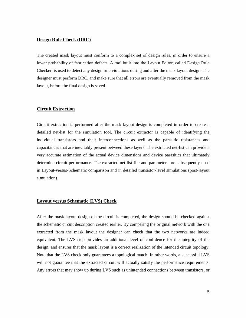
cycle may be repeated several times to accomplish the design objectives. Fig.1.3 shows the
sequence of physical design.
SystemPartitioning
Floorplanning
Placement
Routing
Post−layoutSimulation
CircuitExtraction
Fig.1.3 A Typical Physical Design Flow [MJS].
Partitioning Step
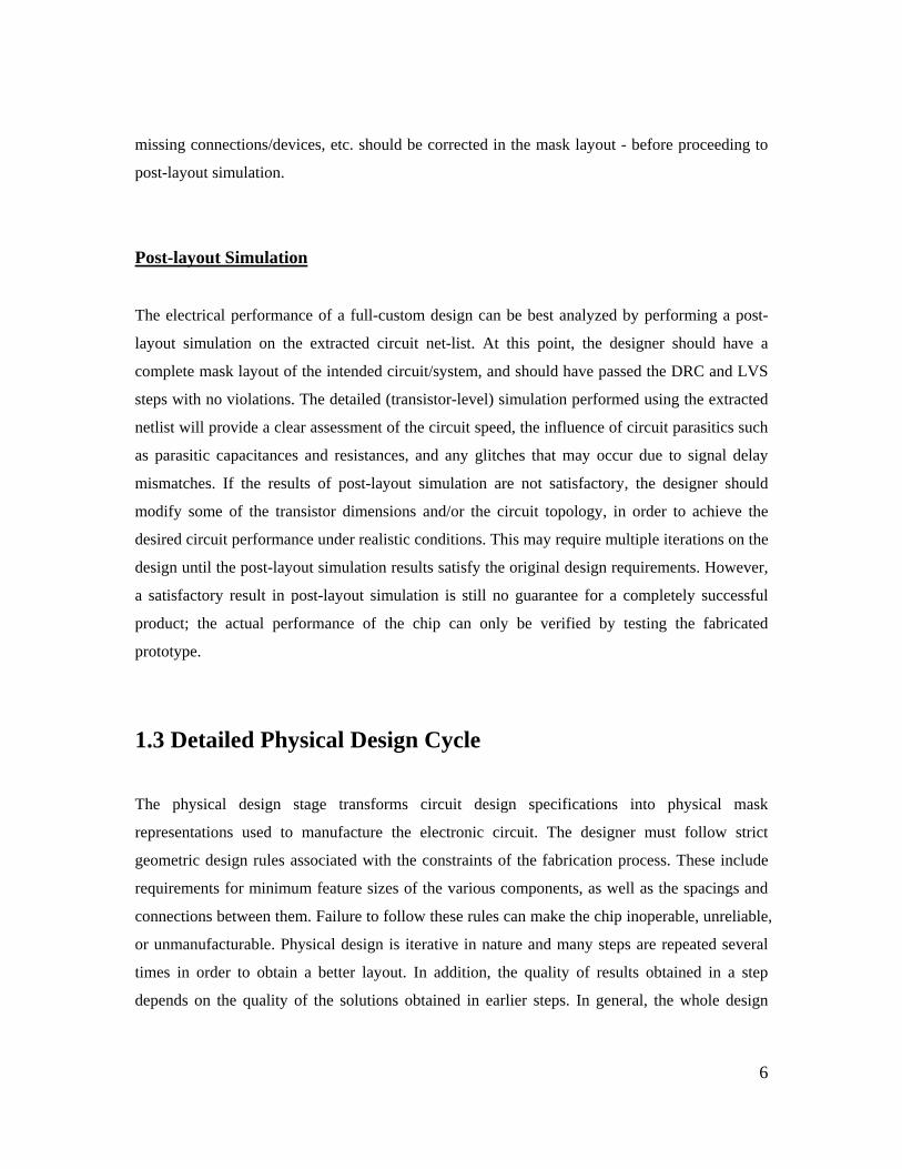
A chip may contain several million transistors. The layout of the whole chip cannot be handled
due to the limitation of memory space, as well as computation time. Therefore, it is normally
partitioned by grouping components into blocks as shown in Fig.1.4. The actual partitioning
process considers many factors such as the size of the blocks, the number of blocks and the
number of interconnections between the blocks. The output of partitioning is a set of blocks
along with the interconnections required between blocks. In large circuits, the partitioning
process is hierarchical and at the top-most level a chip may have between 5 to 25 blocks. Each
module is then partitioned recursively into smaller blocks.
8
Fig.1.4 A simple example of partitioning
Floor-planning and Placement Step
This step is concerned with selecting good layout alternatives for each block as well as the entire
chip. The area of each block can be calculated after partitioning and is based approximately on
the number and the type of components in that block. The actual rectangular shape of the block,
which is determined by the aspect ratio may vary within a pre-specified range. In executing a
complex layout, it is worthwhile to develop a plan for how the various subcells are to be placed
and connected. This process is generally referred to as floorplanning. A well-done floorplan
greatly minimizes area and routing complexity and can even simplify subcell layout. Thus, very
often, the task of floor-plan layout is done by a design engineer, rather than by a CAD tool. This
is sometimes necessary as the major components of an IC are often intended for specific
locations on the chip.
A critical part of floorplanning is deciding which signals travel in which tracks and how far.
Since it is assumed that a track passes completely over any leaf cell without interference, the
importance of not using the upper metal layers within the subcells should be obvious. Exceptions
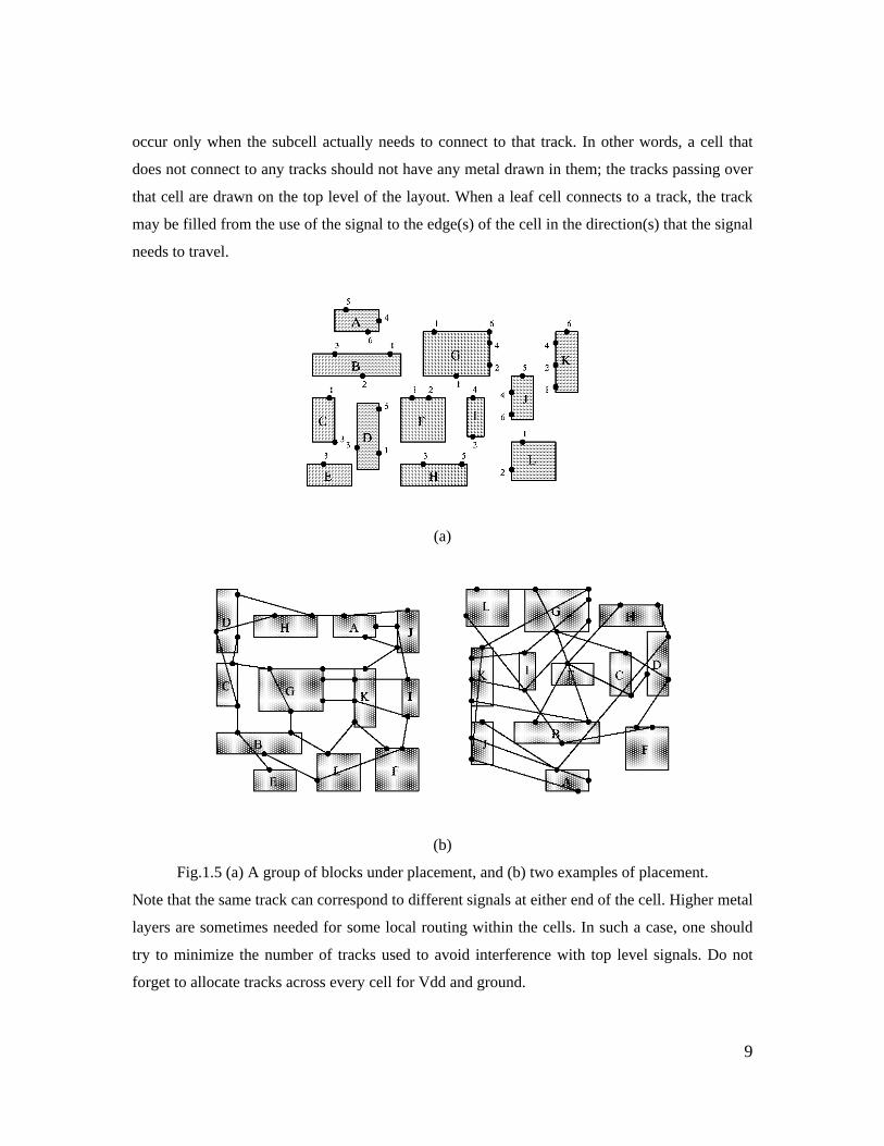
9
occur only when the subcell actually needs to connect to that track. In other words, a cell that
does not connect to any tracks should not have any metal drawn in them; the tracks passing over
that cell are drawn on the top level of the layout. When a leaf cell connects to a track, the track
may be filled from the use of the signal to the edge(s) of the cell in the direction(s) that the signal
needs to travel.
(a)
(b)
Fig.1.5 (a) A group of blocks under placement, and (b) two examples of placement.
Note that the same track can correspond to different signals at either end of the cell. Higher metal
layers are sometimes needed for some local routing within the cells. In such a case, one should
try to minimize the number of tracks used to avoid interference with top level signals. Do not
forget to allocate tracks across every cell for Vdd and ground.
10
During placement, the blocks are exactly positioned on the chip. As shown in Fig.1.5, the goal
of placement is to find a minimum area arrangement for the blocks that allows completion of
interconnections between the blocks. Placement is typically done in two phases. In the first phase,
an initial placement is created. In the second phase, the initial placement is evaluated and
iterative improvements are made until the layout has minimum area and conforms to design
specifications. Between adjacent cells, interconnection is as simple as ensuring that the signal in
each cell goes all the way to the edge of the cell at the same location on the common edge. In this
way, the mere placement of the cells adjacent to each other in the next level of layout hierarchy
connects the two cells properly. This eliminates the need to manually connect adjacent cells on
the top level and helps to guide the layout of the leaf cells. However, it also requires that the leaf
cell layouts meet design rule requirements when placed adjacent to each other.
The quality of the placement will not be evident until the routing phase has been completed.
Placement may lead to an un-routable design, i.e., routing may not be possible in the space
provided. In that case, another iteration of placement is necessary. To limit the number of
iterations of the placement algorithm, an estimate of the required routing space is used during the
placement phase. Good routing and circuit performance heavily depend on a good placement
algorithm. This is due to the fact that once the position of each block is fixed, very little can be
done to improve the routing and the overall circuit performance.
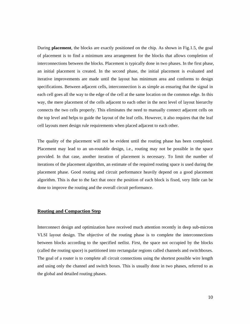
Routing and Compaction Step
Interconnect design and optimization have received much attention recently in deep sub-micron
VLSI layout design. The objective of the routing phase is to complete the interconnections
between blocks according to the specified netlist. First, the space not occupied by the blocks
(called the routing space) is partitioned into rectangular regions called channels and switchboxes.
The goal of a router is to complete all circuit connections using the shortest possible wire length
and using only the channel and switch boxes. This is usually done in two phases, referred to as
the global and detailed routing phases.
11
(a) (b)
Fig.1.6 (a) Global Routing, and (b) Detailed Routing
Global routing is often planned with the aid of these channels and tracks. Channels are areas of
a die between functional units used exclusively for routing. They are often highly oblong to
accommodate long buses. Because most metal layers in a channel are used for routing, it is
usually not possible to put devices into the channels. Routing tracks are used to organize and
simplify routing within and over layout cells. Generally, global routing layers (the higher metal
layers) are assigned a preferred direction that alternates every layer. Usually this direction
restriction does not apply to the lowest one or two metal layers because of their use in
convoluted local routes. Picture the entire layout overlaid with minimum width metal lines
running the length of the bit slice. The lines are at the minimum pitch which allows space for via
landing pads to upper and lower metal layers. Each of these hypothetical metal lines is referred
to as a track. Global routing is followed by detailed routing, which completes point-to-point
connections between pins on the blocks. Loose routing is converted into exact routing by
specifying geometric information such as width of wires and their layer assignments.
Compaction is simply the task of compressing the layout in all directions such that the total area
is reduced. By making the chip smaller, wire lengths are reduced which in turn reduces the signal
delay between components of the circuit. At the same time, this reduced area implies that more
chips can be produced on a single wafer driving down the cost of manufacturing. Compaction
must ensure that no rules regarding the design and fabrication process are violated during the
process.

12
Extraction
Circuit extractors analyze the layout and extract a netlist of transistors, thus converting a physical
description back to a structural description. The structural circuit description can then be
simulated with a switch or circuit simulator. Programs to verify the extracted netlist include: a
network comparison program, which compares the netlist from the circuit design phase to the
extracted netlist from the physical design; and an electrical rules checker (ERC), which checks
the electrical properties of a circuit. Parameter extractors can determine electrical parameters
from layout information for timing simulation.
Post-Layout Simulation
Finally, post-layout simulation ensures that the chosen design performs all the desired functions
with extracted parameters. This simulation also helps determine the circuit's operating speed and
checks any delays accurately.

13
References
[MOO] Gordon E. Moore, “ Cramming More Components onto Integrated Circuits,” Electronics.
Vol.38, April 19, 1965.
[MJS] Michael John Sebastian and John Smith, Application-Specific Integrated Circuits,
Wesley Publishing Company, 1997.
14
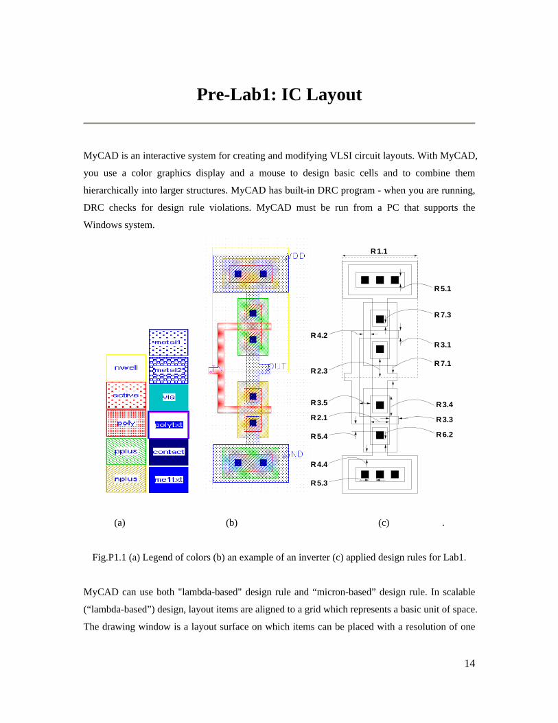
Pre-Lab1: IC Layout
MyCAD is an interactive system for creating and modifying VLSI circuit layouts. With MyCAD,
you use a color graphics display and a mouse to design basic cells and to combine them
hierarchically into larger structures. MyCAD has built-in DRC program - when you are running,
DRC checks for design rule violations. MyCAD must be run from a PC that supports the
Windows system.
R 7.3
R 3.5 R 3.4
R 1.1
R 2.3R 7.1
R 3.1
R 5.4
R 2.1
R 4.4
R 4.2
R 6.2
R 3.3
R 5.1
R 5.3
(a) (b) (c) .
Fig.P1.1 (a) Legend of colors (b) an example of an inverter (c) applied design rules for Lab1.
MyCAD can use both "lambda-based" design rule and “micron-based” design rule. In scalable
(“lambda-based”) design, layout items are aligned to a grid which represents a basic unit of space.
The drawing window is a layout surface on which items can be placed with a resolution of one
15
lambda. In this lab, the given DRC rule is based on lambda rule, and one lambda is 0.5um. While
drawing an inverter, however, your feature sizes are shown in micrometers in the MyChip layout
editor.
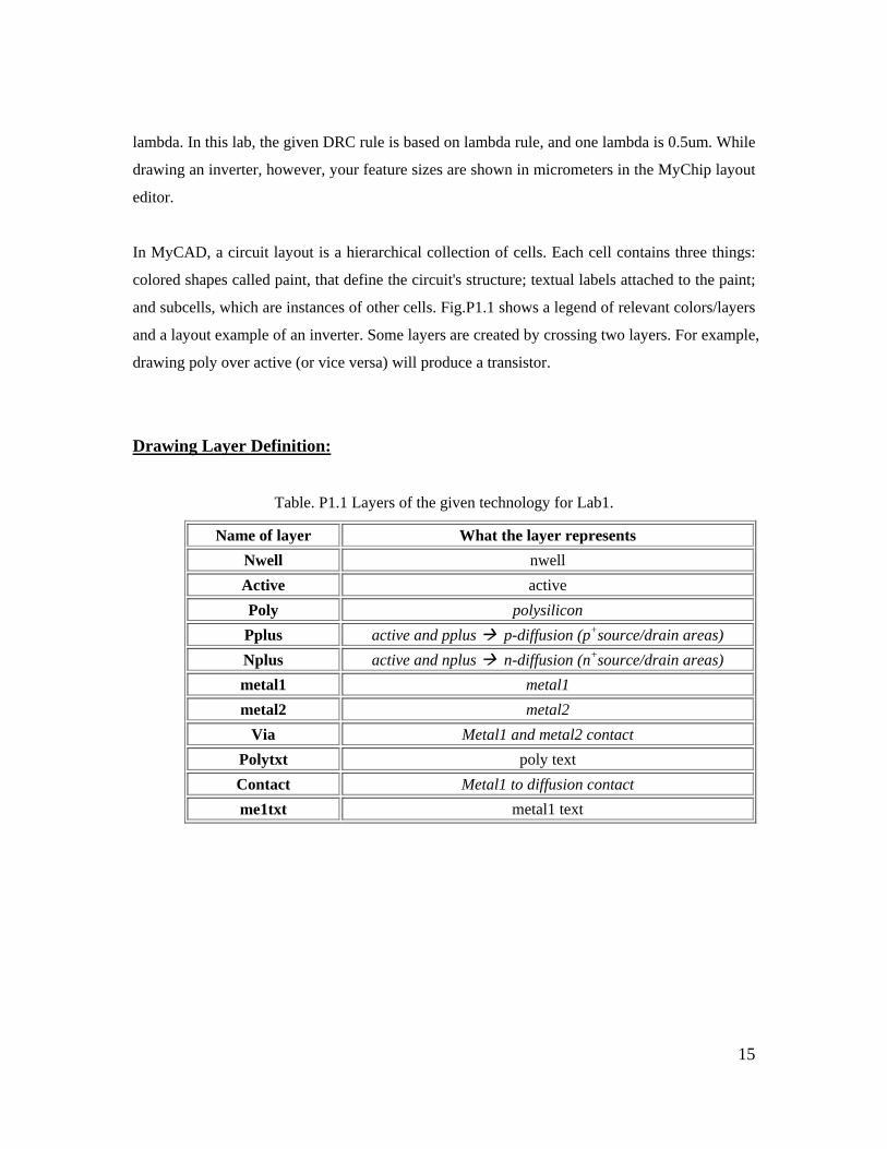
In MyCAD, a circuit layout is a hierarchical collection of cells. Each cell contains three things:
colored shapes called paint, that define the circuit's structure; textual labels attached to the paint;
and subcells, which are instances of other cells. Fig.P1.1 shows a legend of relevant colors/layers
and a layout example of an inverter. Some layers are created by crossing two layers. For example,
drawing poly over active (or vice versa) will produce a transistor.
Drawing Layer Definition:
Table. P1.1 Layers of the given technology for Lab1.
Name of layer What the layer represents Nwell nwell Active active Poly polysilicon
Pplus active and pplus p-diffusion (p+source/drain areas) Nplus active and nplus n-diffusion (n+source/drain areas)metal1 metal1 metal2 metal2
Via Metal1 and metal2 contact Polytxt poly text Contact Metal1 to diffusion contact me1txt metal1 text
16
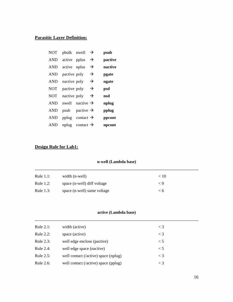
Parasitic Layer Definition:
NOT pbulk nwell psub
AND active pplus pactive
AND active nplus nactive
AND pactive poly pgate
AND nactive poly ngate
NOT pactive poly psd
NOT nactive poly nsd
AND nwell nactive nplug
AND psub pactive pplug
AND pplug contact ppcont
AND nplug contact npcont
Design Rule for Lab1:
n-well (Lambda base)
Rule 1.1: width (n-well) < 10
Rule 1.2: space (n-well) diff voltage < 9
Rule 1.3: space (n-well) same voltage < 6
active (Lambda base)
Rule 2.1: width (active) < 3
Rule 2.2: space (active) < 3
Rule 2.3: well edge enclose (pactive) < 5
Rule 2.4: well edge space (nacitve) < 5
Rule 2.5: well contact (/active) space (nplug) < 3
Rule 2.6: well contact (/active) space (pplug) < 3
17
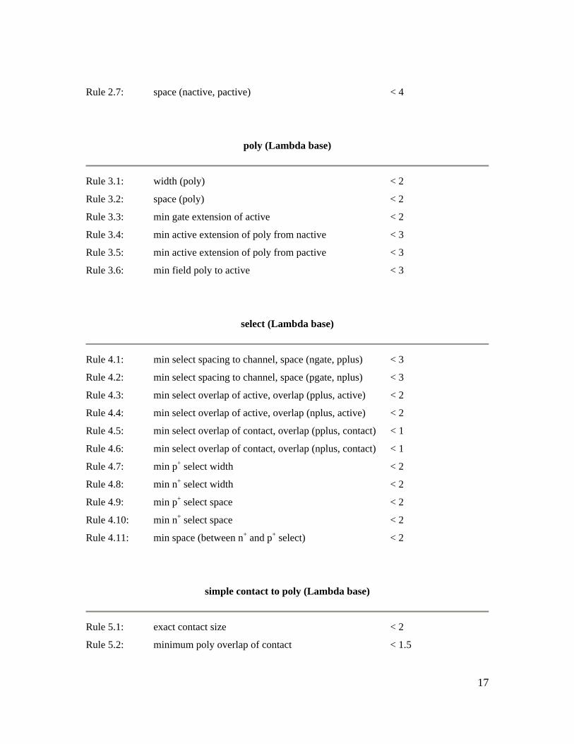
Rule 2.7: space (nactive, pactive) < 4
poly (Lambda base)
Rule 3.1: width (poly) < 2
Rule 3.2: space (poly) < 2
Rule 3.3: min gate extension of active < 2
Rule 3.4: min active extension of poly from nactive < 3
Rule 3.5: min active extension of poly from pactive < 3
Rule 3.6: min field poly to active < 3
select (Lambda base)
Rule 4.1: min select spacing to channel, space (ngate, pplus) < 3
Rule 4.2: min select spacing to channel, space (pgate, nplus) < 3
Rule 4.3: min select overlap of active, overlap (pplus, active) < 2
Rule 4.4: min select overlap of active, overlap (nplus, active) < 2
Rule 4.5: min select overlap of contact, overlap (pplus, contact) < 1
Rule 4.6: min select overlap of contact, overlap (nplus, contact) < 1
Rule 4.7: min p+ select width < 2
Rule 4.8: min n+ select width < 2
Rule 4.9: min p+ select space < 2
Rule 4.10: min n+ select space < 2
Rule 4.11: min space (between n+ and p+ select) < 2
simple contact to poly (Lambda base)
Rule 5.1: exact contact size < 2
Rule 5.2: minimum poly overlap of contact < 1.5
18
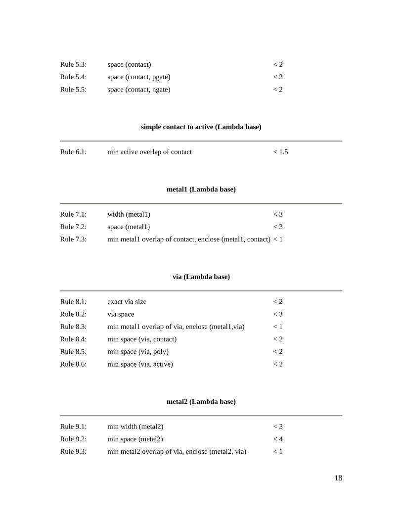
Rule 5.3: space (contact) < 2
Rule 5.4: space (contact, pgate) < 2
Rule 5.5: space (contact, ngate) < 2
simple contact to active (Lambda base)
Rule 6.1: min active overlap of contact < 1.5
metal1 (Lambda base)
Rule 7.1: width (metal1) < 3
Rule 7.2: space (metal1) < 3
Rule 7.3: min metal1 overlap of contact, enclose (metal1, contact) < 1
via (Lambda base)
Rule 8.1: exact via size < 2
Rule 8.2: via space < 3
Rule 8.3: min metal1 overlap of via, enclose (metal1,via) < 1
Rule 8.4: min space (via, contact) < 2
Rule 8.5: min space (via, poly) < 2
Rule 8.6: min space (via, active) < 2
metal2 (Lambda base)
Rule 9.1: min width (metal2) < 3
Rule 9.2: min space (metal2) < 4
Rule 9.3: min metal2 overlap of via, enclose (metal2, via) < 1
19
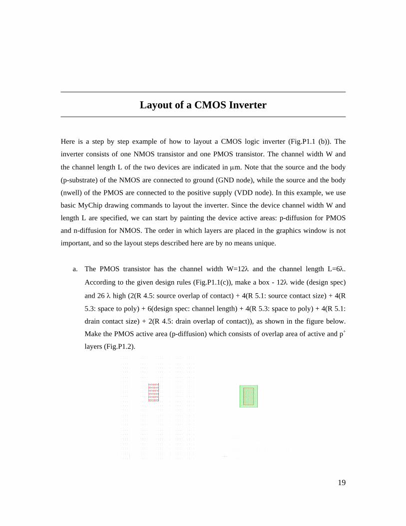
Layout of a CMOS Inverter
Here is a step by step example of how to layout a CMOS logic inverter (Fig.P1.1 (b)). The
inverter consists of one NMOS transistor and one PMOS transistor. The channel width W and
the channel length L of the two devices are indicated in μm. Note that the source and the body
(p-substrate) of the NMOS are connected to ground (GND node), while the source and the body
(nwell) of the PMOS are connected to the positive supply (VDD node). In this example, we use
basic MyChip drawing commands to layout the inverter. Since the device channel width W and
length L are specified, we can start by painting the device active areas: p-diffusion for PMOS
and n-diffusion for NMOS. The order in which layers are placed in the graphics window is not
important, and so the layout steps described here are by no means unique.
a. The PMOS transistor has the channel width W=12λ and the channel length L=6λ.
According to the given design rules (Fig.P1.1(c)), make a box - 12λ wide (design spec)
and 26 λ high (2(R 4.5: source overlap of contact) + 4(R 5.1: source contact size) + 4(R
5.3: space to poly) + 6(design spec: channel length) + 4(R 5.3: space to poly) + 4(R 5.1:
drain contact size) + 2(R 4.5: drain overlap of contact)), as shown in the figure below.
Make the PMOS active area (p-diffusion) which consists of overlap area of active and p+
layers (Fig.P1.2).
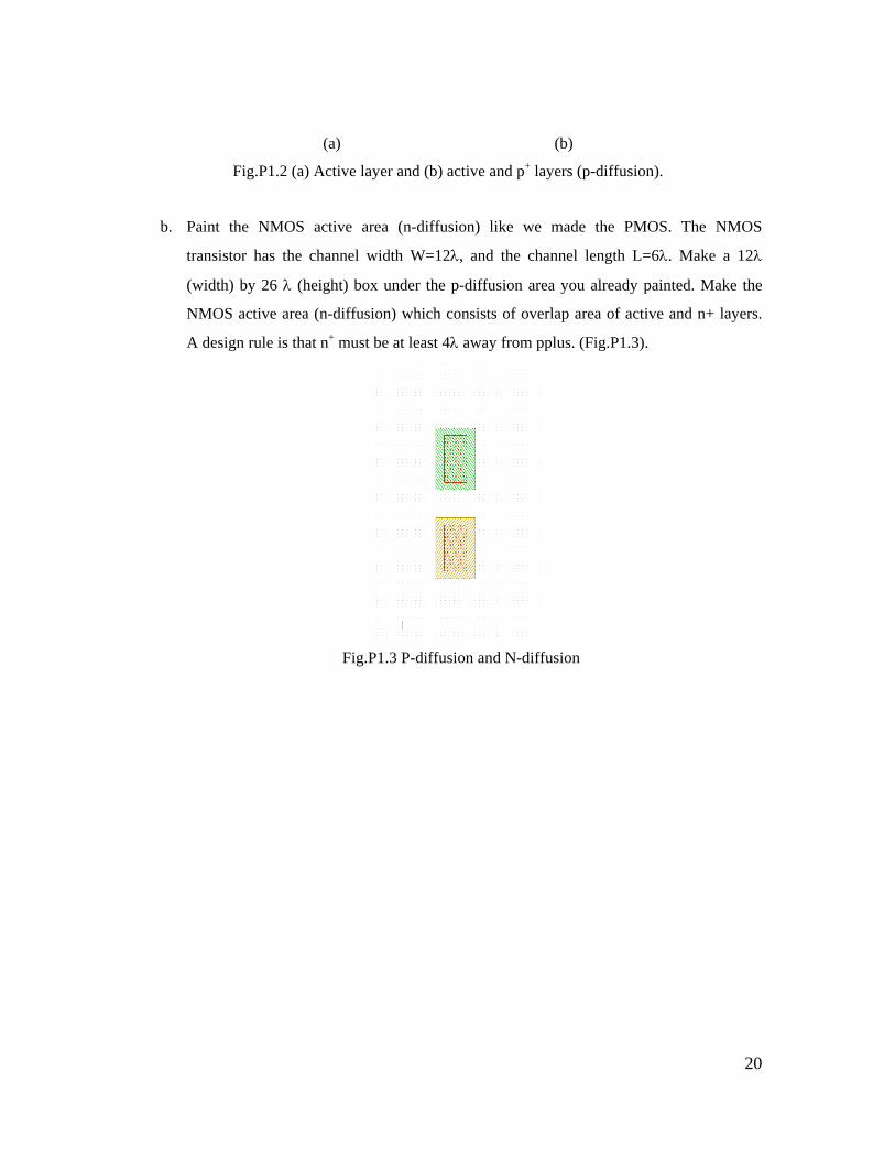
20
(a) (b)
Fig.P1.2 (a) Active layer and (b) active and p+ layers (p-diffusion).
b. Paint the NMOS active area (n-diffusion) like we made the PMOS. The NMOS
transistor has the channel width W=12λ, and the channel length L=6λ. Make a 12λ
(width) by 26 λ (height) box under the p-diffusion area you already painted. Make the
NMOS active area (n-diffusion) which consists of overlap area of active and n+ layers.
A design rule is that n+ must be at least 4λ away from pplus. (Fig.P1.3).
Fig.P1.3 P-diffusion and N-diffusion
21
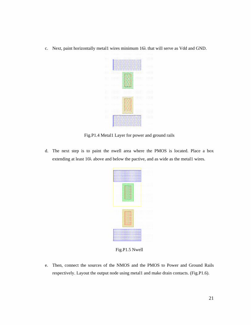
c. Next, paint horizontally metal1 wires minimum 16λ that will serve as Vdd and GND.
Fig.P1.4 Metal1 Layer for power and ground rails
d. The next step is to paint the nwell area where the PMOS is located. Place a box
extending at least 10λ above and below the pactive, and as wide as the metal1 wires.
Fig.P1.5 Nwell
e. Then, connect the sources of the NMOS and the PMOS to Power and Ground Rails
respectively. Layout the output node using metal1 and make drain contacts. (Fig.P1.6).
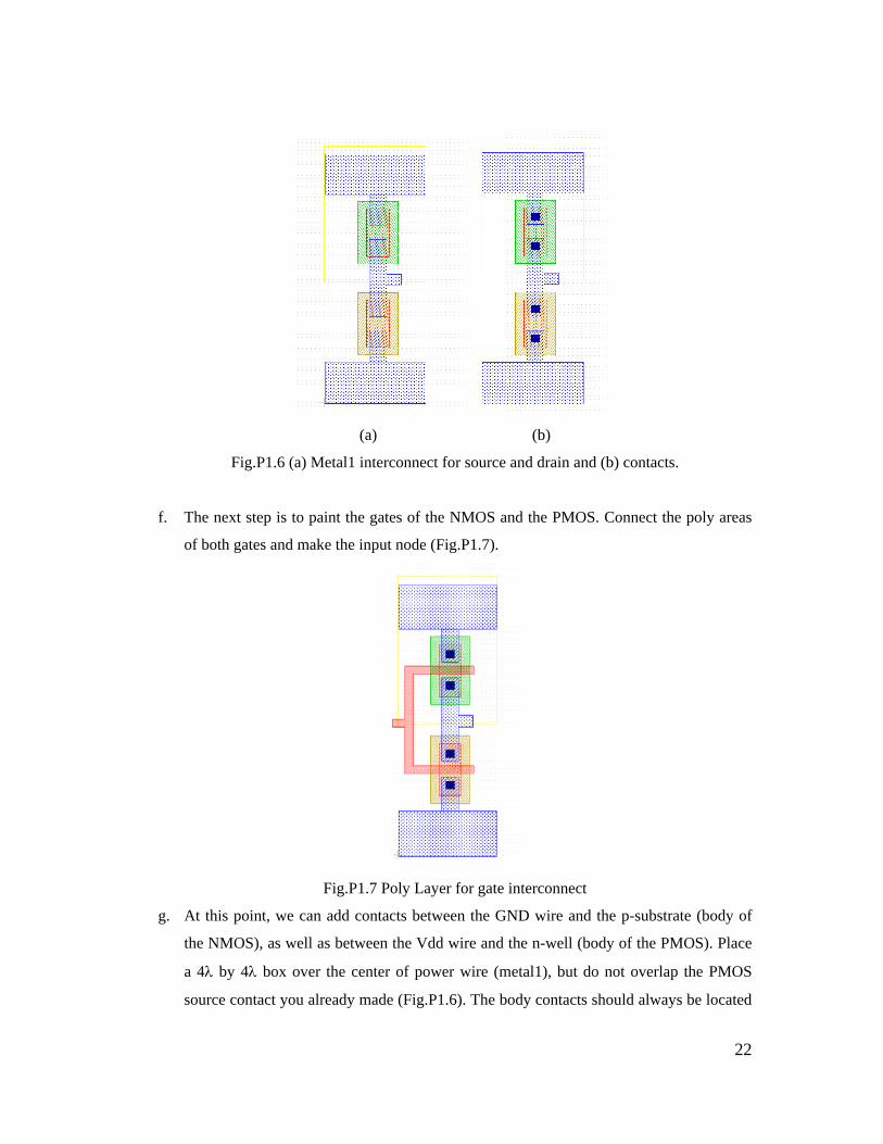
22
(a) (b)
Fig.P1.6 (a) Metal1 interconnect for source and drain and (b) contacts.
f. The next step is to paint the gates of the NMOS and the PMOS. Connect the poly areas
of both gates and make the input node (Fig.P1.7).
Fig.P1.7 Poly Layer for gate interconnect
g. At this point, we can add contacts between the GND wire and the p-substrate (body of
the NMOS), as well as between the Vdd wire and the n-well (body of the PMOS). Place
a 4λ by 4λ box over the center of power wire (metal1), but do not overlap the PMOS
source contact you already made (Fig.P1.6). The body contacts should always be located
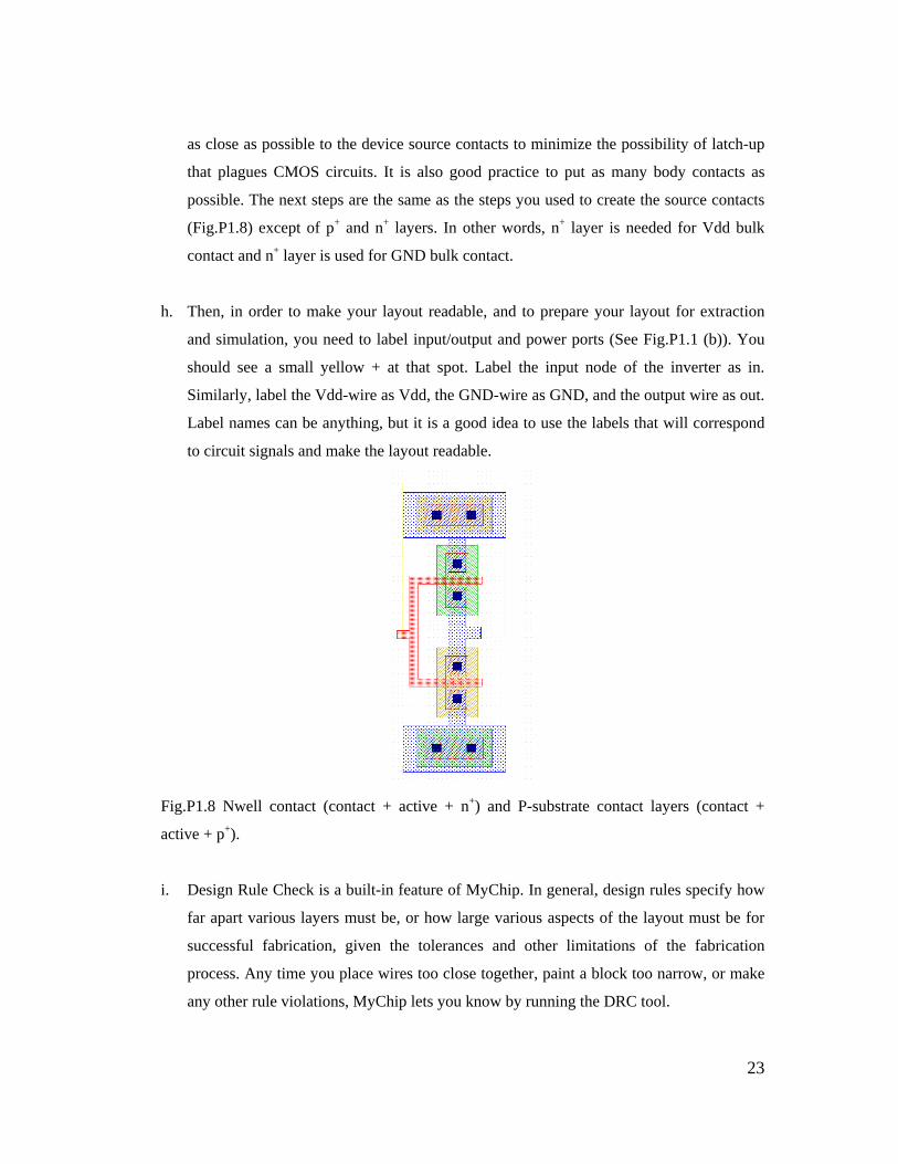
23
as close as possible to the device source contacts to minimize the possibility of latch-up
that plagues CMOS circuits. It is also good practice to put as many body contacts as
possible. The next steps are the same as the steps you used to create the source contacts
(Fig.P1.8) except of p+ and n+ layers. In other words, n+ layer is needed for Vdd bulk
contact and n+ layer is used for GND bulk contact.
h. Then, in order to make your layout readable, and to prepare your layout for extraction
and simulation, you need to label input/output and power ports (See Fig.P1.1 (b)). You
should see a small yellow + at that spot. Label the input node of the inverter as in.
Similarly, label the Vdd-wire as Vdd, the GND-wire as GND, and the output wire as out.
Label names can be anything, but it is a good idea to use the labels that will correspond
to circuit signals and make the layout readable.
Fig.P1.8 Nwell contact (contact + active + n+) and P-substrate contact layers (contact +
active + p+).
i. Design Rule Check is a built-in feature of MyChip. In general, design rules specify how
far apart various layers must be, or how large various aspects of the layout must be for
successful fabrication, given the tolerances and other limitations of the fabrication
process. Any time you place wires too close together, paint a block too narrow, or make
any other rule violations, MyChip lets you know by running the DRC tool.

24
j. The built-in MyChip extractor generates from the layout the netlist needed to run
simulation tool—AimSpice. The netlist includes the sizes and shapes of the transistors,
and the connectivity, resistance, and parasitic capacitances of the nodes.
Related Documents