ALC5631Q I 2 C +I 2 S Audio Codec Stereo Class-D Amp Cap-Free Headphone Amp Datasheet Rev. 0.9 Realtek Semiconductor Corp. No. 2, Innovation Road II, Hsinchu Science Park, Hsinchu 300, Taiwan Tel.: +886-3-578-0211. Fax: +886-3-577-6047 www.realtek.com

Welcome message from author
This document is posted to help you gain knowledge. Please leave a comment to let me know what you think about it! Share it to your friends and learn new things together.
Transcript
ALC5631Q
I2C +I2S Audio Codec Stereo Class-D Amp
Cap-Free Headphone Amp
Datasheet
Rev. 0.9
Realtek Semiconductor Corp. No. 2, Innovation Road II, Hsinchu Science Park, Hsinchu 300, Taiwan
Tel.: +886-3-578-0211. Fax: +886-3-577-6047
www.realtek.com

ALC5631Q Datasheet
I2S Audio Codec + Class-D Amp + Cap-Free HP ii Rev. 0.9
COPYRIGHT ©2011 Realtek Semiconductor Corp. All rights reserved. No part of this document may be reproduced, transmitted, transcribed, stored in a retrieval system, or translated into any language in any form or by any means without the written permission of Realtek Semiconductor Corp.
DISCLAIMER Realtek provides this document “as is”, without warranty of any kind. Realtek may make improvements and/or changes in this document or in the product described in this document at any time. This document could include technical inaccuracies or typographical errors.
TRADEMARKS Realtek is a trademark of Realtek Semiconductor Corporation. Other names mentioned in this document are trademarks/registered trademarks of their respective owners.
USING THIS DOCUMENT This document is intended for the hardware and software engineer’s general information on the Realtek ALC5631Q Audio Codec IC.
Though every effort has been made to ensure that this document is current and accurate, more information may have become available subsequent to the production of this guide.

ALC5631Q Datasheet
I2S Audio Codec + Class-D Amp + Cap-Free HP iii Rev. 0.9
REVISION HISTORY Revision Release Date Summary
0.1 2010/03/01 Preliminary version 0.11 2010/3/17 Fix typing error 0.2 2010/4/20 1. Modify package pin definition
2. Add note at mixer path 3. Modify ALC block 4. Modify pin location for typing error 5. Modify application circuit
0.3 2010/5/4 1. Modify Figure 3 2. Modify application circuit 3. add more description
0.4 2010/8/18 1. Modify some typing error 2. Modify Application circuit 3. Modify order information to “Sample”
0.5 2010/9/21 1. Modify performance information 2. Modify application circuit
0.61 2010/9/27 1. Modify some typos 0.62 2010/12/13 1. Modify typos in register list
2. Update operation voltage for AVDD 3. Modify application circuit
0.9 2011/1/20 1. Modify registers 2. Modify mixer path

ALC5631Q Datasheet
I2S Audio Codec + Class-D Amp + Cap-Free HP iv Rev. 0.9
Table of Contents 1. GENERAL DESCRIPTION..............................................................................................................................................1
2. FEATURES.........................................................................................................................................................................1
3. SYSTEM APPLICATION .................................................................................................................................................2
4. FUNCTION BLOCK AND MIXER PATH .....................................................................................................................2 4.1. FUNCTION BLOCK ........................................................................................................................................................2 4.2. AUDIO MIXER PATH.....................................................................................................................................................3
5. PIN ASSIGNMENTS .........................................................................................................................................................4 5.1. GREEN PACKAGE AND VERSION IDENTIFICATION ........................................................................................................4
6. PIN DESCRIPTIONS.........................................................................................................................................................5 6.1. DIGITAL I/O PINS .........................................................................................................................................................5 6.2. ANALOG I/O PINS ........................................................................................................................................................6 6.3. FILTER/REFERENCE......................................................................................................................................................7 6.4. POWER/GROUND..........................................................................................................................................................7
7. FUNCTION DESCRIPTION ............................................................................................................................................8 7.1. POWER .........................................................................................................................................................................8 7.2. RESET ..........................................................................................................................................................................8
7.2.1. Power-On Reset (POR) ..........................................................................................................................................9 7.2.2. H/W Reset ...............................................................................................................................................................9 7.2.3. Software Reset ........................................................................................................................................................9
7.3. CLOCKING....................................................................................................................................................................9 7.3.1. Phase-Locked Loop ..............................................................................................................................................10 7.3.2. I2C and Stereo I2S.................................................................................................................................................10
7.4. DIGITAL DATA INTERFACE ........................................................................................................................................11 7.4.1. Stereo I2S/PCM Interface .....................................................................................................................................11
7.5. AUDIO DATA PATH ....................................................................................................................................................14 7.5.1. Stereo ADC...........................................................................................................................................................14 7.5.2. Stereo DAC...........................................................................................................................................................14 7.5.3. Mixers...................................................................................................................................................................14
7.6. ANALOG AUDIO INPUT PATH .....................................................................................................................................15 7.7. ANALOG AUDIO OUTPUT PATH..................................................................................................................................16 7.8. ALC FUNCTION .........................................................................................................................................................17 7.9. SPEAKER AMPLIFIER RATIO GAIN..............................................................................................................................20 7.10. HARDWARE SOUND PROCESSING...............................................................................................................................21
7.10.1. Equalizer Block................................................................................................................................................21 7.10.2. Pseudo Stereo and Spatial 3D Sound ..............................................................................................................21 7.10.3. Wind Noise Reduction Filter............................................................................................................................21
7.11. I2C CONTROL INTERFACE ..........................................................................................................................................22 7.11.1. Address Setting ................................................................................................................................................22 7.11.2. Complete Data Transfer ..................................................................................................................................22 7.11.3. Odd-Addressed Register Access ......................................................................................................................23
7.12. GPIO, INTERRUPT AND JACK DETECTION ..................................................................................................................23 7.13. POWER MANAGEMENT...............................................................................................................................................25
8. REGISTERS LIST ...........................................................................................................................................................26 8.1. REG-00H: RESET ........................................................................................................................................................26
ALC5631Q Datasheet
I2S Audio Codec + Class-D Amp + Cap-Free HP v Rev. 0.9
8.2. REG-02H: SPEAKER OUTPUT CONTROL .....................................................................................................................26 8.3. REG-04H: HEADPHONE OUTPUT CONTROL ................................................................................................................27 8.4. REG-06H: OUTPUT CONTROL FOR AXO1/AXO2/MONOOUT .................................................................................28 8.5. REG-0AH: AUX INPUT VOLUME CONTROL .............................................................................................................29 8.6. REG-0CH: STEREO DAC CONTROL 1 ......................................................................................................................29 8.7. REG-0EH: MICROPHONE INPUT CONTROL .................................................................................................................30 8.8. REG-10H: STEREO DAC CONTROL 2 .......................................................................................................................30 8.9. REG-12H: STEREO ADC CONTROL 1..........................................................................................................................30 8.10. REG-14H: ADC RECORDING MIXER CONTROL ..........................................................................................................31 8.11. REG-16H: STEREO ADC CONTROL 2..........................................................................................................................32 8.12. REG-1AH: LEFT OUTPUT MIXER (OUTMIXL) CONTROL..........................................................................................32 8.13. REG-1CH: RIGHT OUTPUT MIXER (OUTMIXR) MIXER CONTROL............................................................................33 8.14. REG-1EH: AXO1MIX CONTROL ...............................................................................................................................33 8.15. REG-20H: AXO2MIX CONTROL................................................................................................................................35 8.16. REG-22H: MICROPHONE INPUT CONTROL..................................................................................................................36 8.17. REG-24H: DIGITAL MICROPHONE CONTROL ..............................................................................................................37 8.18. REG-26H: MONOIN INPUT VOLUME.........................................................................................................................38 8.19. REG-28H: SPEAKER MIXER CONTROL........................................................................................................................38 8.20. REG-2AH: SPEAKER/MONO OUTPUT CONTROL .........................................................................................................39 8.21. REG-2CH: SPEAKER/MONO/HP OUTPUT CONTROL ...................................................................................................41 8.22. REG-34H: STEREO I2S SERIAL DATA PORT CONTROL ................................................................................................42 8.23. REG-38H: STEREO ADC/DAC CLOCK CONTROL.......................................................................................................43 8.24. REG-3AH: POWER MANAGEMENT 1...........................................................................................................................44 8.25. REG-3BH: POWER MANAGEMENT 2...........................................................................................................................45 8.26. REG-3CH: POWER MANAGEMENT 3...........................................................................................................................46 8.27. REG-3EH: POWER MANAGEMENT 4 ...........................................................................................................................47 8.28. REG-40H: GENERAL PURPOSE CONTROL REGISTER...................................................................................................48 8.29. REG-42H: GLOBAL CLOCK CONTROL ........................................................................................................................49 8.30. REG-44H: PLL CONTROL...........................................................................................................................................49
8.30.1. PLL Clock Setting Table for 48K: (Unit: MHz)...............................................................................................50 8.30.2. PLL Clock Setting Table for 44.1K: (Unit: MHz)............................................................................................50
8.31. REG-48H: INTERNAL STATUS AND IRQ CONTROL 1 ..................................................................................................50 8.32. REG-4AH: INTERNAL STATUS AND IRQ CONTROL 2..................................................................................................51 8.33. REG-4CH: GPIO CONTROL ........................................................................................................................................51 8.34. REG-52H: MISC. CONTROL .......................................................................................................................................52 8.35. REG-56H: DE-POP FUNCTION CONTROL ...................................................................................................................54 8.36. REG-5AH: JACK DETECTION CONTROL......................................................................................................................55 8.37. REG-5CH: SOFT VOLUME CONTROL ..........................................................................................................................57 8.38. REG-64H: ALC CONTROL 1 .......................................................................................................................................58 8.39. REG-65H: ALC CONTROL 2 .......................................................................................................................................59 8.40. REG-66H: ALC CONTROL 3 .......................................................................................................................................59 8.41. REG-68H: PSEUDO STEREO AND SPATIAL EFFECT CONTROL .....................................................................................60 8.42. REG-6AH: INDEX ADDRESS .......................................................................................................................................61 8.43. REG-6CH: INDEX DATA .............................................................................................................................................61 8.44. REG-6EH: EQ CONTROL 1 .........................................................................................................................................61 8.45. INDEX-00H: EQ LOW PASS FILTER COEFFICIENT (LPF: A1) ......................................................................................63 8.46. INDEX-01H: EQ LOW PASS FILTER GAIN (LPF: HO)..................................................................................................63 8.47. INDEX-02H: EQ BAND PASS FILTER 1 COEFFICIENT (BPF1: A1)................................................................................63 8.48. INDEX-03H: EQ BAND PASS FILTER 1 COEFFICIENT (BPF1: A2)................................................................................63 8.49. INDEX-04H: EQ BAND PASS FILTER 1 GAIN (BPF1: HO) ...........................................................................................64 8.50. INDEX-05H: EQ BAND PASS FILTER 2 COEFFICIENT (BPF2: A1)................................................................................64 8.51. INDEX-06H: EQ BAND PASS FILTER 2 COEFFICIENT (BPF2: A2)................................................................................64 8.52. INDEX-07H: EQ BAND PASS FILTER 2 GAIN (BPF2: HO) ...........................................................................................64 8.53. INDEX-08H: EQ BAND PASS FILTER 3 COEFFICIENT (BPF3: A1)................................................................................65 8.54. INDEX-09H: EQ BAND PASS FILTER 3 COEFFICIENT (BPF3: A2)................................................................................65
ALC5631Q Datasheet
I2S Audio Codec + Class-D Amp + Cap-Free HP vi Rev. 0.9
8.55. INDEX-0AH: EQ BAND PASS FILTER 3 GAIN (BPF3: HO) ..........................................................................................65 8.56. INDEX-0BH: EQ HIGH PASS FILTER 1 COEFFICIENT (HPF1: A1)................................................................................65 8.57. INDEX-0CH: EQ HIGH PASS FILTER 1 GAIN (HPF1: HO) ...........................................................................................66 8.58. INDEX-0DH: EQ HIGH PASS FILTER 2 COEFFICIENT (HPF2: A1) ...............................................................................66 8.59. INDEX-0EH: EQ HIGH PASS FILTER 2 COEFFICIENT (HPF2: A2)................................................................................66 8.60. INDEX-0FH: EQ HIGH PASS FILTER 2 GAIN (HPF2: HO)............................................................................................66 8.61. INDEX-11H: EQ INPUT VOLUME CONTROL ................................................................................................................66 8.62. INDEX-12H: EQ OUTPUT VOLUME CONTROL.............................................................................................................67 8.63. INDEX-20H: ALC DAC DIGITAL VOLUME.................................................................................................................67 8.64. INDEX-21H: AUTO VOLUME CONTROL REGISTER 1 ...................................................................................................68 8.65. INDEX-22H: AUTO VOLUME CONTROL REGISTER 2 ...................................................................................................69 8.66. INDEX-23H: AUTO LEVEL CONTROL REGISTER 3 ....................................................................................................71 8.67. INDEX-4AH: CLASS-D INTERNAL REGISTER.............................................................................................................71 8.68. REG-7CH: VENDOR ID 1 ............................................................................................................................................72
9. ELECTRICAL CHARACTERISTICS ..........................................................................................................................73 9.1. DC CHARACTERISTICS...............................................................................................................................................73
9.1.1. Absolute Maximum Ratings ..................................................................................................................................73 9.1.2. Recommended Operating Conditions ...................................................................................................................73 9.1.3. Static Characteristics ...........................................................................................................................................73
9.2. ANALOG PERFORMANCE CHARACTERISTICS..............................................................................................................74 9.3. SIGNAL TIMING..........................................................................................................................................................77
9.3.1. I2C Control Interface............................................................................................................................................77 9.3.2. I2S/PCM Interface Master Mode ..........................................................................................................................78 9.3.3. I2S/PCM Interface Slave Mode.............................................................................................................................79
10. APPLICATION CIRCUITS .......................................................................................................................................80
11. MECHANICAL DIMENSIONS.................................................................................................................................81
12. ORDERING INFORMATION...................................................................................................................................82

ALC5631Q Datasheet
I2S Audio Codec + Class-D Amp + Cap-Free HP vii Rev. 0.9
List of Tables TABLE 1. DIGITAL I/O PINS ..........................................................................................................................................................5 TABLE 2. ANALOG I/O PINS..........................................................................................................................................................6 TABLE 3. FILTER/REFERENCE .......................................................................................................................................................7 TABLE 4. POWER/GROUND ...........................................................................................................................................................7 TABLE 5. POWER SUPPLY FOR BEST PERFORMANCE.....................................................................................................................8 TABLE 6. POWER SUPPLY FOR LEAKAGE CURRENT ......................................................................................................................8 TABLE 7. RESET OPERATION ........................................................................................................................................................8 TABLE 8. POWER-ON RESET VOLTAGE.........................................................................................................................................9 TABLE 9. CLOCK SETTING TABLE FOR 48K (UNIT: MHZ) ..........................................................................................................10 TABLE 10. CLOCK SETTING TABLE FOR 44.1K (UNIT: MHZ) .....................................................................................................10 TABLE 11. RATION GAIN TABLE FOR SPKVDD .........................................................................................................................20 TABLE 12. SAMPLE RATE WITH BANDWIDTH FOR WIND FILTER.................................................................................................21 TABLE 13. ADDRESS SETTING (0X34H).......................................................................................................................................22 TABLE 13. WRITE WORD PROTOCOL ........................................................................................................................................22 TABLE 14. READ WORD PROTOCOL..........................................................................................................................................22 TABLE 14. REG-00H: RESET .......................................................................................................................................................26 TABLE 15. REG-02H: SPEAKER OUTPUT CONTROL.....................................................................................................................26 TABLE 16. REG-04H: HEADPHONE OUTPUT CONTROL ...............................................................................................................27 TABLE 17. REG-06H: OUTPUT CONTROL FOR AXO1/AXO2/MONOOUT.................................................................................28 TABLE 18. REG-0AH: AUX INPUT VOLUME CONTROL ............................................................................................................29 TABLE 19. REG-0CH: STEREO DAC CONTROL 1......................................................................................................................29 TABLE 20. REG-0EH: MICROPHONE INPUT CONTROL.................................................................................................................30 TABLE 21. REG-10H: STEREO DAC CONTROL 2 ......................................................................................................................30 TABLE 22. REG-12H: STEREO ADC CONTROL 1 .........................................................................................................................30 TABLE 23. REG-14H: ADC RECORDING MIXER CONTROL .........................................................................................................31 TABLE 24. REG-16H: STEREO ADC CONTROL 2 .........................................................................................................................32 TABLE 25. REG-1AH: LEFT OUTPUT MIXER CONTROL...............................................................................................................32 TABLE 26. REG-1CH: RIGHT OUTPUT MIXER CONTROL.............................................................................................................33 TABLE 27. REG-1EH: AXO1 MIXER CONTROL...........................................................................................................................34 TABLE 28. REG-20H: AXO2 MIXER CONTROL ...........................................................................................................................35 TABLE 29. REG-22H: MICROPHONE INPUT CONTROL .................................................................................................................36 TABLE 30. REG-24H: DIGITAL MICROPHONE CONTROL .............................................................................................................37 TABLE 31. REG-26H: MONOIN INPUT VOLUME ........................................................................................................................38 TABLE 32. REG-28H: SPEAKER MIXER CONTROL .......................................................................................................................38 TABLE 33. REG-2AH: SPEAKER/MONO OUTPUT CONTROL ........................................................................................................39 TABLE 34. REG-2CH: SPEAKER/MONO/HP OUTPUT CONTROL...................................................................................................41 TABLE 35. REG-34H: STEREO I2S SERIAL DATA PORT CONTROL ...............................................................................................42 TABLE 36. REG-38H: STEREO ADC/DAC CLOCK CONTROL ......................................................................................................43 TABLE 37. REG-3AH: POWER MANAGEMENT 1 ..........................................................................................................................44 TABLE 38. REG-3BH: POWER MANAGEMENT 2 ..........................................................................................................................45 TABLE 39. REG-3CH: POWER MANAGEMENT 3 ..........................................................................................................................46 TABLE 40. REG-3EH: POWER MANAGEMENT 4 ..........................................................................................................................47 TABLE 41. REG-40H: GENERAL PURPOSE CONTROL REGISTER ..................................................................................................48 TABLE 42. REG-42H: GLOBAL CLOCK CONTROL........................................................................................................................49 TABLE 43. REG-44H: PLL CONTROL ..........................................................................................................................................49 TABLE 44. PLL CLOCK SETTING TABLE FOR 48K: (UNIT: MHZ) ...............................................................................................50 TABLE 45. PLL CLOCK SETTING TABLE FOR 44.1K: (UNIT: MHZ) ............................................................................................50 TABLE 46. REG-48H: INTERNAL STATUS AND IRQ CONTROL 1..................................................................................................50 TABLE 47. REG-4AH: INTERNAL STATUS AND IRQ CONTROL 2 .................................................................................................51 TABLE 48. REG-4CH: GPIO CONTROL .......................................................................................................................................52 TABLE 49. REG-52H: MISC. CONTROL.......................................................................................................................................52 TABLE 50. REG-54H: DE-POP FUNCTION CONTROL 1................................................................................................................53

ALC5631Q Datasheet
I2S Audio Codec + Class-D Amp + Cap-Free HP viii Rev. 0.9
TABLE 51. REG-56H: DE-POP FUNCTION CONTROL...................................................................................................................54 TABLE 52. REG-5AH: JACK DETECTION CONTROL .....................................................................................................................55 TABLE 53. REG-5CH: SOFT VOLUME CONTROL..........................................................................................................................57 TABLE 54. REG-64H: ALC CONTROL 1.......................................................................................................................................58 TABLE 55. REG-65H: ALC CONTROL 2.......................................................................................................................................59 TABLE 56. REG-66H: ALC CONTROL 3.......................................................................................................................................59 TABLE 57. REG-68H: PSEUDO STEREO AND SPATIAL EFFECT CONTROL.....................................................................................60 TABLE 58. REG-6AH: INDEX ADDRESS.......................................................................................................................................61 TABLE 59. REG-6CH: INDEX DATA.............................................................................................................................................61 TABLE 60. REG-6EH: EQ CONTROL 1.........................................................................................................................................61 TABLE 61. INDEX-00H: EQ LOW PASS FILTER COEFFICIENT (LPF: A1)......................................................................................63 TABLE 62. INDEX-01H: EQ LOW PASS FILTER GAIN (LPF: HO) .................................................................................................63 TABLE 63. INDEX-02H: EQ BAND PASS FILTER 1 COEFFICIENT (BPF1: A1) ...............................................................................63 TABLE 64. INDEX-03H: EQ BAND PASS FILTER 1 COEFFICIENT (BPF1: A2) ...............................................................................64 TABLE 65. INDEX-04H: EQ BAND PASS FILTER 1 GAIN (BPF1: HO) ..........................................................................................64 TABLE 66. INDEX-05H: EQ BAND PASS FILTER 2 COEFFICIENT (BPF2: A1) ...............................................................................64 TABLE 67. INDEX-06H: EQ BAND PASS FILTER 2 COEFFICIENT (BPF2: A2) ...............................................................................64 TABLE 68. INDEX-07H: EQ BAND PASS FILTER 2 GAIN (BPF2: HO) ..........................................................................................64 TABLE 69. INDEX-08H: EQ BAND PASS FILTER 3 COEFFICIENT (BPF3: A1) ...............................................................................65 TABLE 70. INDEX-09H: EQ BAND PASS FILTER 3 COEFFICIENT (BPF3: A2) ...............................................................................65 TABLE 71. INDEX-0AH: EQ BAND PASS FILTER 3 GAIN (BPF3: HO) .........................................................................................65 TABLE 72. INDEX-0BH: EQ HIGH PASS FILTER 1 COEFFICIENT (HPF1: A1) ...............................................................................65 TABLE 73. INDEX-0CH: EQ HIGH PASS FILTER 1 GAIN (HPF1: HO) ..........................................................................................66 TABLE 74. INDEX-0DH: EQ HIGH PASS FILTER 2 COEFFICIENT (HPF1: A1)...............................................................................66 TABLE 75. INDEX-0EH: EQ HIGH PASS FILTER 2 COEFFICIENT (HPF1: A2) ...............................................................................66 TABLE 76. INDEX-0FH: EQ HIGH PASS FILTER 2 GAIN (HPF2: HO)...........................................................................................66 TABLE 77. INDEX-11H: EQ INPUT VOLUME CONTROL ...............................................................................................................67 TABLE 78. INDEX-12H: EQ OUTPUT VOLUME CONTROL............................................................................................................67 TABLE 79. INDEX-20XXH: ALC DAC DIGITAL VOLUME ..........................................................................................................67 TABLE 80. INDEX-21H: AUTO VOLUME CONTROL REGISTER 1 ..................................................................................................68 TABLE 81. INDEX-22H: AUTO VOLUME CONTROL REGISTER 2 ..................................................................................................69 TABLE 82. INDEX-23H: AUTO LEVEL CONTROL REGISTER 3 ......................................................................................................71 TABLE 83. INDEX-4AH: CLASS-D INTERNAL REGISTER..............................................................................................................71 TABLE 84. REG-7CH: VENDOR ID 1 ...........................................................................................................................................72 TABLE 85. ABSOLUTE MAXIMUM RATINGS................................................................................................................................73 TABLE 86. RECOMMENDED OPERATING CONDITIONS.................................................................................................................73 TABLE 87. STATIC CHARACTERISTICS ........................................................................................................................................73 TABLE 88. ANALOG PERFORMANCE CHARACTERISTICS .............................................................................................................74 TABLE 89. THERMAL INFORMATION...........................................................................................................................................76 TABLE 90. I2C TIMING ................................................................................................................................................................77 TABLE 91. TIMING OF I2S/PCM MASTER MODE.........................................................................................................................78 TABLE 92. I2S/PCM SLAVE MODE TIMING.................................................................................................................................79 TABLE 93. ORDERING INFORMATION..........................................................................................................................................82
ALC5631Q Datasheet
I2S Audio Codec + Class-D Amp + Cap-Free HP ix Rev. 0.9
List of Figures FIGURE 1. BLOCK DIAGRAM .......................................................................................................................................................2 FIGURE 2. AUDIO MIXER PATH ...................................................................................................................................................3 FIGURE 3. PIN ASSIGNMENTS ......................................................................................................................................................4 FIGURE 4. AUDIO SYSCLK ........................................................................................................................................................9 FIGURE 5. PCM MONO DATA MODE A FORMAT (BCLK POLARITY=0) ..............................................................................11 FIGURE 6. PCM MONO DATA MODE A FORMAT (BCLK POLARITY=1) ..............................................................................12 FIGURE 7. PCM MONO DATA MODE B FORMAT (BCLK POLARITY=0) ..............................................................................12 FIGURE 8. PCM STEREO DATA MODE A FORMAT (BCLK POLARITY=0)..............................................................................12 FIGURE 9. PCM STEREO DATA MODE B FORMAT (BCLK POLARITY=0) ..............................................................................13 FIGURE 10. I2S DATA FORMAT (BCLK POLARITY=0) ...........................................................................................................13 FIGURE 11. LEFT-JUSTIFIED DATA FORMAT (BCLK POLARITY=0) ........................................................................................13 FIGURE 12. AUTO LEVEL CONTROL BLOCK DIAGRAM..............................................................................................................17 FIGURE 13. ALC FOR PLAYBACK MODE ...................................................................................................................................18 FIGURE 14. ALC FOR RECORDING MODE..................................................................................................................................19 FIGURE 15. RATIO GAIN FOR SPKVDD AND AVDD ................................................................................................................20 FIGURE 16. DATA TRANSFER OVER I2C CONTROL INTERFACE .................................................................................................22 FIGURE 17. IRQ/JACK DETECTION FUNCTION BLOCK ..............................................................................................................24 FIGURE 18. I2C CONTROL INTERFACE .......................................................................................................................................77 FIGURE 19. TIMING OF I2S/PCM MASTER MODE ......................................................................................................................78 FIGURE 20. I2S/PCM SLAVE MODE TIMING..............................................................................................................................79 FIGURE 21. APPLICATION CIRCUIT............................................................................................................................................80 FIGURE 22. PACKAGE DIMENSION.............................................................................................................................................81

ALC5631Q Datasheet
I2S Audio Codec + Class-D Amp + Cap-Free HP 1 Rev. 0.5
1. General Description The ALC5631Q is a high performance and powerful I2S codec for portable devices. Multi-function configuration for input and output port can flexible for using. Differential input mode can effective to cancel the common-mode noise for input signal. And single-ended input mode can easy be used for external income signal. With wide range volume control can be used for each path whether analog to digital path, analog to analog path or digital to analog path. An analog input to analog output path is bypass ADC and DAC that can keep original performance to output for income signal. In this bypass mode, can into the ultra low power mode by shutdown unused block. The powerful Auto-Level-Control (ALC) function is for playback and record. For playback, it will keep the same output level when different input level. And prevent the output signal be clipped when speaker power is dropping or huge input signal. For record, it can effective to reduce the background noise for voice recording. Wide range power supply and low power consumption on ALC5631Q is suitable for portable devices. Also 48-ball QFN (6mm x 6mm) package is used by ALC5631Q.
2. Features Digital-to-Analog Converter with 100dBA SNR and –90dB THD+N Analog-to-Digital Converter with 93dBA SNR and –88dB THD+N Stereo BTL (Bridge-Tied Load) Class-D amplifier and with 650mW/Ch output power
(SPKVDD=3.6V, THD = 1%, 8Ω load) Stereo headphone output and without DC blocking capacitors.
(With 45mW/Ch driving power, 3.3V, 16Ω load) 3 analog differential inputs and 1 stereo single-ended input Stereo differential analog microphone inputs with boost pre-amplifiers and low noise microphone
bias Differential earpiece Amp output Stereo single-end or one differential line output Audio jack insert detection and microphone switch detection Power management and enhanced power saving Support flexible digital 6 bands equalizer (EQ) Support digital spatial sound and pseudo stereo effect Zero detection and soft volume for pop noise suppression Inside PLL can receive wide range clock input Support I2C Control Interface 24bit/8kHz ~ 192kHz I2S/PCM interface for stereo DAC 24bit/8kHz ~ 96kHz I2S/PCM interface for stereo ADC Support enhanced Auto Level Control (ALC) function for playback and record Support digital microphone interface QFN-48 (6mm x 6mm) package

ALC5631Q Datasheet
I2S Audio Codec + Class-D Amp + Cap-Free HP 2 Rev. 0.9
3. System Application Smartbook Netbook
4. Function Block and Mixer Path
4.1. Function Block
MIC1PMIC1N
MONOIN_PMONOIN_N
AXI_L/JD1AXI_R/JD2
Boost
ADC_L
ADC_R
ALC6-Band EQ3D Effect
DACL
DACR
OutputMixer
Digital Audio Interface
BC
LKLR
CK
DA
CD
AT
AD
CD
AT
AXO1_L/PAXO1_R/N
SPO_LP
SPO_RPSPO_LN
SPO_RN
LDAC
RDAC
SPO_L_VolDRC
SPO_R_VolDRC
I2CControl
SC
LS
DA
MICBIAS1
MICBIAS2PLL
MC
LK
HPO_L_Vol
HPO_R_Vol
LDAC
RDAC
HPO_LHPO_R
CPNCPP
CP_VREFCPVEE
VREF
AV
DD
AG
ND
SPK
DD
2S
PK
GN
D
DC
VD
D
DG
ND
DBV
DD
SPK
DD
1S
PK
GN
D
ADC Volume
High Pass Filter
DAC Volume
High Pass Filter
CP
VD
D
HeadphoneBlock
CP
GN
D
D_S
CL
DMICInterface
D_S
DA/
GPI
O
MICBIAS1
MICBIAS2
ReferenceVoltage
MONO_L_Vol
MONO_R_Vol
MONOOUT_PMONOOUT_N
MIC2PMIC2N
AXO2_L/PAXO2_R/NInput
Mixer
AVDD
AVDD
AVDD
OUT_Vol
Cde
pop
Figure 1. Block Diagram

ALC5631Q Datasheet
I2S Audio Codec + Class-D Amp + Cap-Free HP 3 Rev. 0.9
4.2. Audio Mixer Path
SPOLMIX
OUTMIXL
Class D AMP
SPO_LP
SPO_LN
HPO_L
HPO_R
MONOOUT_P
MONOOUT_N
(-46. 5 ~ +12dB, 1.5dB/step)
(-46. 5 ~ +12dB, 1.5dB/step)
(-46. 5 ~ 0dB, 1.5dB/step)
(-46. 5 ~ 0dB, 1.5dB/step)
SPKVOLL
SPKVOLR
OUTVOLR
OUTVOLL
DACL
AXO1MIX
OUTMIXL
OUTMIXR
-34.5~+12dB,1.5dB/step
-34.5~+12dB,1.5dB/step
-34.5~+12dB,1.5dB/stepMONOIN_P
MONOIN_N
AXIL
RECMIXL
RECMIXR
20/30/40/50
20/30/40/50dB
BST1N
BST2P
BST2N
ADCR
ADCL
DACL
DACR
Filte
r&D
igita
lVol
ume
AD
CD
AT
DA
CD
AT
ALCDRC
3D( Only DAC)EQ
a/u-Law
AD- DA Loop Back
DA- AD Loop Back
Voice ADC
AD- DA Loop Back
DA- AD Loop Back
Loop Back
DSPBlock※
Onl
yO
neof
AD
Can
dD
AC
pass
DSP
AXIR
-34.5~+12dB,1.5dB/step
RXN
RXP
(-46. 5 ~ 0dB, 1.5dB/step)
HPOVOLL
(-46. 5 ~ 0dB, 1.5dB/step)
HPOVOLRDACR
ZCD
Filte
r&D
igita
lVol
ume
Filte
r&D
igita
lVol
ume
Filte
r&D
igita
lVol
ume
SPKMIXL
SPKMIXR
AXO1_R/N
AXO1_L/P
VMID
VMID
BST1PMIC1P
MIC1N
MIC2P
MIC2N
OUTMIXL
RX
RX
AXILVOL
AXIRVOL
BST1
BST2
OUTMIXR
RECMIXL
MIC1P
RECMIXL
DACL
RECMIXR
BST1
BST2
RXN
AXILVOL
AXIRVOL
AXILVOL
AXIRVOL
BST1
BST2
RXP
RECMIXL
RECMIXR
RECMIXR
MIC2P
DACR
sel_lin_hp
sel_rin_hp
ZCD
ZCD
ZCD
VMID
VMID
VMID
VMID
VMID
VMID
VMID
-21 ~ 0dB,3dB/stepBST2PBST2N
-21 ~ 0dB,3dB/stepBST1PBST1N
AXO2MIX
AXO2_R/N
AXO2_L/P
-21~ 0dB,3dB/stepBST2PBST2N
-21~ 0dB,3dB/stepBST1PBST1N
RXPRXN
DACLPDACLN
sel_spol
SPORMIXClass D AMP
SPO_RP
SPO_RN
RXPRXN
DACLPDACLN sel_spor
MONOMIX
RXPRXN
sel_ mono
en_rx_se
REG-0E[15]
REG-22[15:12]
REG-0A[12:8]
REG-26[12:8]
REG-26[4:0]
REG-0A[4:0]
REG-0E[7]
REG-22[11:8]
REG-14[4]
REG-14[5]
REG-14[6]
REG-14[7]
REG-14[15]
REG-14[14]
REG-14[13]
REG-14[12]
REG-28[15]
REG-28[14]
REG-28[13]
REG-28[12]
REG-1A[15]
REG-1A[14]
REG-1A[13]
REG-1A[12]
REG-1A[11]
REG-1A[10]
REG-1A[9]
REG-1A[8]
REG-1C[15]
REG-1C[14]
REG-1C[13]
REG-1C[12]
REG-1C[11]
REG-1C[10]
REG-1C[9]
REG-1C[8]
REG-28[7]
REG-28[6]
REG-28[5]
REG-28[4]
REG-02[5:0]
REG-02[6]
REG-04[4:0]
REG-04[6]
REG-06[4:0]
REG-06[6]
REG-06[14]
REG-06[12:8]
REG-04[12:8]
REG-04[14]
REG-02[13:8]
REG-02[14]
REG-1E[14:12]
REG-1E[10:8]
REG-2A[15]
REG-2A[14]
REG-2A[11]
REG-2A[10]
REG-2A[13]
REG-2A[12]
REG-20[14:12]
REG-20[10:8]
REG-20[15]
REG-20[7]
REG-20[6]
REG-20[11]
REG-02[7]
REG-2C[11:10]
REG-06[13]
REG-2C[7:6]
REG-04[7]REG-2C[2]
REG-02[15]
REG-2C[15:14]
REG-04[15]REG-2C[3]
REG-06[15]
REG-1E[15]
REG-1E[7]
REG-1E[6]
REG-1E[11]
REG-06[7]
OUTMIXR
RECMIXR
RECMIXL
DMICALC
6 Band Equalizer3 D effectA/u-Law
Figure 2. Audio Mixer Path

ALC5631Q Datasheet
I2S Audio Codec + Class-D Amp + Cap-Free HP 4 Rev. 0.9
5. Pin Assignments
Figure 3. Pin Assignments
5.1. Green Package and Version Identification Green package is indicated by a ‘G’ in the location marked ‘y’ in Figure 3. The version number is shown in the location marked ‘v’.

ALC5631Q Datasheet
I2S Audio Codec + Class-D Amp + Cap-Free HP 5 Rev. 0.9
6. Pin Descriptions
6.1. Digital I/O Pins Table 1. Digital I/O Pins
Name Type Pin Description Characteristic Definition DACDAT
I 30 Serial I2S data input Schmitt trigger
(VIL=0.35*DBVDD, VIH=0.65*DBVDD) ADCDAT O 31 Serial I2S data output VOL=0.1*DBVDD, VOH=0.9*DBVDD
BCLK I/O 32
I2S interface serial bit clock Master: VOL =0.1*DVDD, VOH =0.9*DVDD
Slave: Schmitt trigger
LRCK I/O 33
I2S interface synchronous signal Master: VOL =0.1*DVDD, VOH =0.9*DVDD
Slave: Schmitt trigger
SDA I/O 34 I2C serial data Open drain structure
SCL I 35
I2C clock input Schmitt trigger
(VIL=0.35*DBVDD, VIH=0.65*DBVDD)
MCLK I 36
I2S master clock input Schmitt trigger
(VIL=0.35*DBVDD, VIH=0.65*DBVDD)
DMIC_SDA/GPIO
I/O 37
Digital microphone data General purpose input and output
Input: Schmitt trigger
(VIL=0.35*DBVDD, VIH=0.65*DBVDD)
Output: VOL=0.1*DBVDD, VOH =0.9*DBVDD
DMIC_SCL O 38 Digital microphone clock Output: VOL=0.1*DBVDD, VOH =0.9*DBVDD
/RST I 42
Hardware reset Schmitt trigger
(VIL=0.35*DBVDD, VIH=0.65*DBVDD) Total: 10 Pins

ALC5631Q Datasheet
I2S Audio Codec + Class-D Amp + Cap-Free HP 6 Rev. 0.9
6.2. Analog I/O Pins Table 2. Analog I/O Pins
Name Type Pin Description Characteristic Definition AXO2_L/P O 2 Auxiliary output 2
Left output channel Differential positive output channel
Analog output
AXO2_R/N O 3 Auxiliary output 2 Right output channel Differential negative output channel
Analog output
AXO1_R/N O 4 Auxiliary output 1 Right output channel Differential negative output channel
Analog output
AXO1_L/P O 5 Auxiliary output 1 Left output channel Differential positive output channel
Analog output
AXIL/JD1 I 8 Auxiliary left channel input / Jack detection pin 1
Analog input JD threshold: Vil = 0.4V Vih = 1.5V
AXIR/JD2 I 9 Auxiliary right channel input / Jack detection pin 2
Analog input JD threshold: Vil = 0.4V Vih = 1.5V
MONOIN_N I 10 Mono negative differential input Analog input MONOIN_P I 11 Mono positive differential input Analog input MIC1P I 12 Positive differential input for MIC1 Analog input MIC1N I 13 Negative differential input for MIC1 Analog input MIC2N I 14 Negative differential input for MIC2 Analog input MIC2P I 15 Positive differential input for MIC2 Analog input MONOOUT_P O 19 Positive channel output for Mono Amp Analog output MONOOUT_N O 20 Negative channel output for Mono Amp Analog output HPO_R O 28 Right channel for headphone output Analog output HPO_L O 29 Left channel for headphone output Analog output SPO_RP O 43 Right positive speaker output Analog output SPO_RN O 45 Right negative speaker output Analog output SPO_LN O 46 Left negative speaker output Analog output SPO_LP O 48 Left positive speaker output Analog output Total: 20 Pins

ALC5631Q Datasheet
I2S Audio Codec + Class-D Amp + Cap-Free HP 7 Rev. 0.9
6.3. Filter/Reference Table 3. Filter/Reference
Name Type Pin Description Characteristic Definition MICBIAS2 O 6 Bias voltage output for MIC2 Programmable analog DC output MICBIAS1 O 7 Bias voltage output for MIC1 Programmable analog DC output VREF O 17 Internal reference voltage 4.7uf capacitor to analog ground Cdepop O 21 Headphone de-pop capacitor 1.0uf capacitor to analog ground CPREF - 22 0V Reference voltage Analog ground CPP - 24 Charge pump bucket capacitor 2.2uf capacitor to CBN CPN - 26 Charge pump bucket capacitor 2.2uf capacitor to CBP Total: 7 Pins
6.4. Power/Ground Table 4. Power/Ground
Name Type Pin Description Characteristic Definition SPKGND P 1 Speaker ground AVDD P 16 Analog power 2.3V~3.6V AGND P 18 Analog ground CPVDD P 23 Charge pump power 2.3V~3.6V CPGND P 25 Charge pump ground CPVEE P 27 Charge pump negative voltage output 2.2uf capacitor to analog ground DCVDD P 39 Digital core power 1.71V~3.6V DBVDD P 40 Digital I/O power 1.71V~3.6V DGND P 41 Digital ground SPKVDD1 P 44 Speaker AMP power 3.0V~5.0V SPKVDD2 P 47 Speaker AMP power 3.0V~5.0V Total: 11 Pins
ALC5631Q Datasheet
I2S Audio Codec + Class-D Amp + Cap-Free HP 8 Rev. 0.9
7. Function Description
7.1. Power There are different power types in ALC5631Q. DBVDD is for digital I/O power, DCVDD is for digital core power, AVDD is for analog power, CPVDD is for charge pump power and SPKVDD is for speaker amplifier power. The power supplier limit condition are DBVDD DCVDD and SPKVDD ≧ ≧ AVDD = CPVDD , AVDD DCVDD, and for the best performance, our design setting is show on below.≧
Table 5. Power Supply for Best Performance Power DBVDD DCVDD AVDD CPVDD SPKVDD
Setting 3.3V 3.3V 3.3V 3.3V 4.2V
Table 6. Power Supply for Leakage Current Supply Condition DBVDD DCVDD AVDD CPVDD SPKVDD Total Leakage Current
1 Supplied Supplied Supplied Supplied Supplied < 11uA
2 N/A N/A N/A N/A Supplied < 11uA
*For other supply conditions, the total leakage current will large than 11uA. We don’t recommend these supply conditions other than Table 6 listed.
7.2. Reset There are 3 types of reset operation: hardware reset, power on reset (POR) and register reset.
Table 7. Reset Operation Reset Type Trigger Condition CODEC Response H/W Reset Control /RST pin from high to low Reset all hardware logic and all registers to default
values. POR Monitor digital power supply voltage reach
VPOR Reset all hardware logic and all registers to default values.
Register Reset Write REG-00h Reset all registers to default values except some specify control registers and logic.

ALC5631Q Datasheet
I2S Audio Codec + Class-D Amp + Cap-Free HP 9 Rev. 0.9
7.2.1. Power-On Reset (POR) When powered on, DCVDD passes through the VPOR band of the ALC5631Q (VPOR_ON ~VPOR_OFF). A power on reset (POR) will generate an internal reset signal (POR reset ‘LOW’) to reset the whole chip.
Table 8. Power-On Reset Voltage Symbol Min Typical Max Unit VPOR_ON 1.0 - 1.6 V VPOR_OFF - 1.3 - V
Note: VPOR_OFF must be below VPOR_ON.
7.2.2. H/W Reset When control /RST pin from high to low, it will reset all hardware logic and reset the registers to default values. The /RST is a Schmitt trigger input. The VIL is equal to 0.35*DBVDD and VIH is equal to 0.65*DBVDD.
7.2.3. Software Reset When REG-00h is wrote, all registers become to default value.
7.3. Clocking The system clock of ALC5631Q can be selected from MCLK or PLL. This means MCLK is always provided externally, and the driver should arrange the clock of each block and setup each divider. The system clock of ALC5631Q can be selected from MCLK or PLLs. MCLK is always provided externally while the reference clock of PLLs can be selected from MCLK, BCLK. The driver should arrange the clock of each block and setup each divider. The Main I2S_SYSCLK=256*Fs(main) provides clocks into stereo DAC/ADC that can be selected from MCLK or PLL. Refer to
sel_
sysc
lk1
sel_
pll_
sour
1
Figure 4. Audio SYSCLK

ALC5631Q Datasheet
I2S Audio Codec + Class-D Amp + Cap-Free HP 10 Rev. 0.9
7.3.1. Phase-Locked Loop A Phase-Locked Loop (PLL) is used to provide a flexible input clock from 2.048MHz to 40MHz. The source of the PLL can be set to MCLK or BCLK by setting register.
The driver can set up the PLL to output a frequency to match the requirement of Main I2S SYSCLK.
The PLL transmit formula is:
FOUT = (MCLK * (N+2)) / ((M+2) * (K+2)) {Typical K=2}
Table 9. Clock Setting Table for 48K (Unit: MHz) MCLK N M FVCO K FOUT
13 66 7 98.222 2 24.555 3.6864 78 1 98.304 2 24.576 2.048 94 0 98.304 2 24.576 4.096 70 1 98.304 2 24.576
12 80 8 98.4 2 24.6 15.36 81 11 98.068 2 24.517
16 78 11 98.462 2 24.615 19.2 80 14 98.4 2 24.6
19.68 78 14 98.4 2 24.6
Table 10. Clock Setting Table for 44.1K (Unit: MHz) MCLK N M FVCO K FOUT
13 68 8 91 2 22.75 3.6864 72 1 90.931 2 22.733 2.048 86 0 90.112 2 22.528 4.096 64 1 90.112 2 22.528
12 66 7 90.667 2 22.667 15.36 63 9 90.764 2 22.691
16 66 10 90.667 2 22.667 19.2 64 12 90.514 2 22.629
19.68 67 13 90.528 2 22.632
After a POR Reset, PLL related Registers are reset to default values, however, they are not reset to default values after a soft-reset (write REG-00).
7.3.2. I2C and Stereo I2S The ALC5631Q supports I2C for the digital control interface, and has I2S/PCM for the digital data interface. The I2S/PCM audio digital interface is used to input data to a stereo DAC or output data from a stereo ADC. The I2S/PCM audio digital interface can be configured to Master mode or Slave mode.

ALC5631Q Datasheet
I2S Audio Codec + Class-D Amp + Cap-Free HP 11 Rev. 0.9
Master Mode In master mode BCLK and LRCK are configured as output. When MCLK is used as I2S SYSCLK source, PLL can be disabled and sel_sysclk1=00’b, . When PLL output is used as I2S SYSCLK source PLL enabled and sel_sysclk1=01’b, MCLK is suggested to provide frequency from 2.048MHz to 40MHz., and PLL should be configured to support .256 or 512*Fs. The driver should set each divider (Reg42 and Reg38) to arrange the clock distribution. Refer to section TBD for details.
Slave Mode In slave mode BCLK and LRCK are configured as input. The_SYSCLK can be input from MCLK by provide the BCLK synchronized clock externally. And the driver should set each divider to arrange the clock distribution. Refer to section TBD for details.
7.4. Digital Data Interface 7.4.1. Stereo I2S/PCM Interface The stereo I2S/PCM interface can be configured as master mode or slave mode. Four audio data formats are supported:
• PCM mode
• Left justified mode
• I2S mode
Figure 5. PCM MONO Data Mode A Format (BCLK POLARITY=0)

ALC5631Q Datasheet
I2S Audio Codec + Class-D Amp + Cap-Free HP 12 Rev. 0.9
Figure 6. PCM MONO Data Mode A Format (BCLK POLARITY=1)
Figure 7. PCM MONO Data Mode B Format (BCLK POLARITY=0)
Figure 8. PCM Stereo Data Mode A Format (BCLK POLARITY=0)
ALC5631Q Datasheet
I2S Audio Codec + Class-D Amp + Cap-Free HP 13 Rev. 0.9
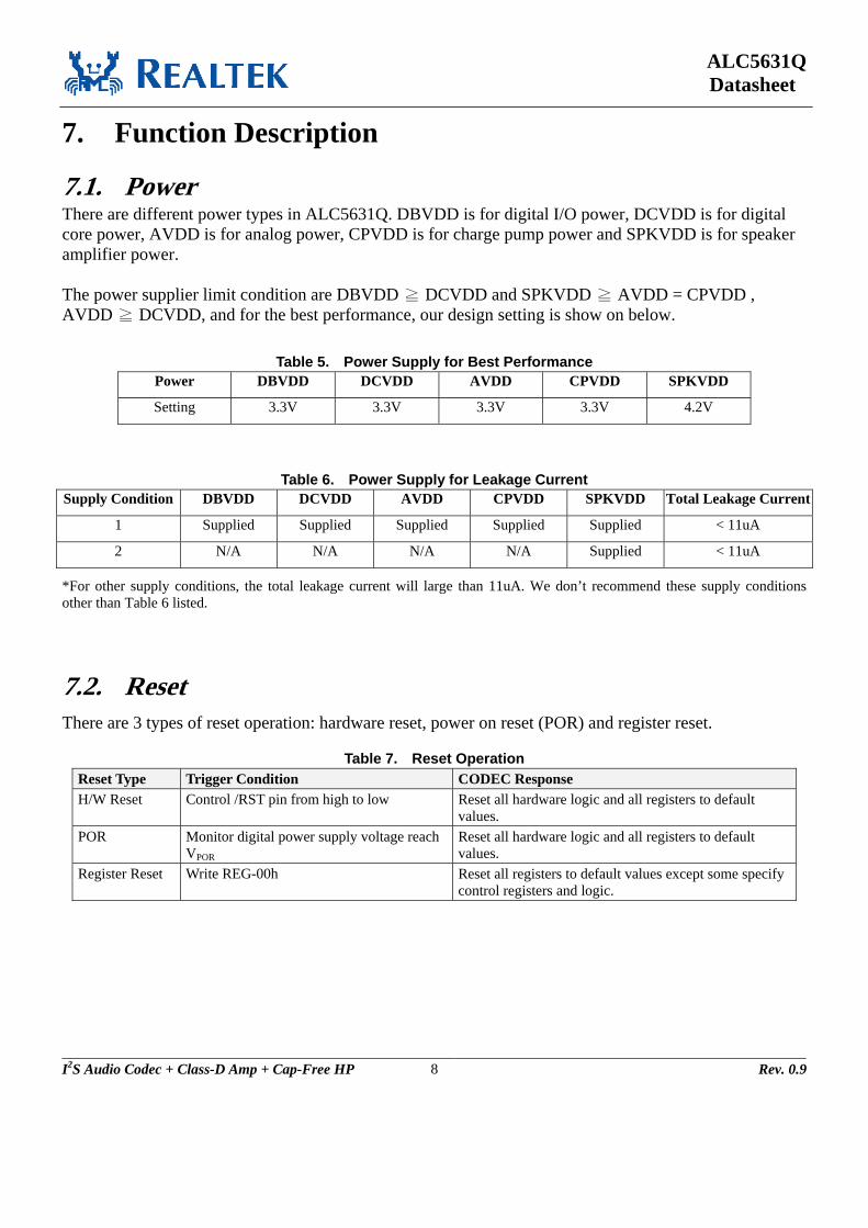
Figure 9. PCM Stereo Data Mode B Format (BCLK POLARITY=0)
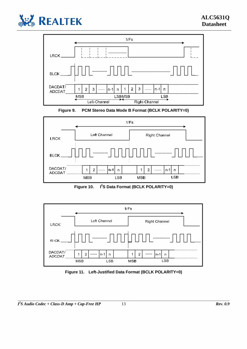
Figure 10. I2S Data Format (BCLK POLARITY=0)
Figure 11. Left-Justified Data Format (BCLK POLARITY=0)
ALC5631Q Datasheet
I2S Audio Codec + Class-D Amp + Cap-Free HP 14 Rev. 0.9
7.5. Audio Data Path The ALC5631Q provides 2-channel stereo audio DAC for playback and 2-channel ADC for recording.
7.5.1. Stereo ADC The stereo ADC is a high performance ADC. The full scale input of ADC is 1Vrms at AVDD is 3.3V. In order to save power, the left and right ADC can be powered down separately by setting pow_adc_l and pow_adc_r . The volume control of the stereo ADC is also can set by vol_adc_l and vol_adc_r .
7.5.2. Stereo DAC The stereo DAC is a high performance DAC. The sampling rate can be configured by setting the stereo I2S clock divider(Reg-38). The volume control of the stereo DAC is set by vol_dac_l and vol_dac_r.
pow_dac_l can be enabled Left channel of DAC whilt pow_dac_r can be enabled Right channel of DAC,
7.5.3. Mixers There are five digital/analog mixers in ALC5631Q.
• Output mixer - OUTMIXL/R
The stereo analog mixer can do mixing for DAC output and analog input. The mixer output is mainly for headphone output. Each input path has it’s mute function to the mixer block in Reg-1A and Reg-1C. pow_outmix and pow_outmixr can be used to power on/off OUTMIXL/R
• Speaker mixer – SPKMIXL/R
The stereo analog mixer can do mixing for OUTMIX output and analog input. The mixer output is for speaker output. Each input path has it’s mute function to the mixer block in Reg-28. pow_spkmixl and pow_spkmixr can be used to power on/off SPKMIXL/R.
• AUX_Out mixer – AXO1/2MIX
The stereo analog mixer can do mixing for analog input and DAC output. The mixer output is for line-out output for drive external amplifier. Each input path has individual mute function to the mixer block in Reg-1E. pow_axo1 and pow_axo2 can be used to power on/off AXOMIX.
• Record mixer – RECMIXL/R
The stereo analog mixer can do mixing for analog input and OUTMIX output. The mixer output is for ADC input. Each input path has it’s mute function to the mixer block in Reg-14. pow_recmixl and pow_recmixr can be used to power on/off RECMIXL/R
• DMIC mixer – DMICMIX
The stereo digital mixer can do mixing for digital microphone input and ADC output. The mixer output is digital data and send to I2S output. en_dmic can be used to power on/off DMICMIX.

ALC5631Q Datasheet
I2S Audio Codec + Class-D Amp + Cap-Free HP 15 Rev. 0.9
# Each mixer has it’s power down control by register. And can power down single channel of stereo mixer independent. It can easy to control the power management to achieve enhance power saving.
7.6. Analog Audio Input Path The ALC5631Q supports four analog audio input ports: • MIC1P/N
The microphone input port-1 can configure as mono differential input or mono single-ended input by REG-0E[15]. The microphone input port has it’s microphone bias and microphone boost. High performance microphone bias can improve the recording performance and increase the microphone sensitivity. Multi-steps microphone boost gain set by sel_bst1 can easy to use for microphone application.
pow_mic1 can be used to power down the MIC1 boost while pow_micbias1 can be used to power down the microphone bias of MIC1.
• MIC2P/N
The microphone input port-2 can configure as mono differential input or mono single-ended input by REG-0E[7].. The microphone input port has it’s microphone bias and microphone boost. High performance microphone bias can improve the recording performance and increase the microphone sensitivity. Multi-steps microphone boost gain set by sel_bst2 can easy to use for microphone application.
pow_mic2 can be used to power down the MIC2 boost while pow_micbias2 can be used to power down the microphone bias of MIC2.
• AXIL/R
The input port is a stereo single-ended input. It has input volume for tuning. The volume range is from +12dB to -34.5dB and with 1.5dB/step. set by REG-0A[12:8] and REG-0A[4:0].
pow_axi_vol_l and pow_axi_vol_r can be used to power down AXIL/R Volume control.
• MONOIN_P/N
This input port can configure as mono differential input or mono single-ended input by en_rx_df.. The input port can direct bypass to mono AMP output or speaker AMP output and don’t need through the internal mixer. It can keep the original performance and minimize the power consumption of inter-chip. The differential input mode can effective to reduce the common-mode noise produced by external device and external PCB trace. It also has input volume control and with +12dB to -34.5dB,

ALC5631Q Datasheet
I2S Audio Codec + Class-D Amp + Cap-Free HP 16 Rev. 0.9
1.5dB/step volume range controlled by REG-26[12:8] and REG-26[4:0]..
7.7. Analog Audio Output Path The ALC5631Q supports four type output paths: • SPO_L/R_P/N
The speaker output of ALC5631Q is a stereo BTL output with Class-D type amplifier. The power of speaker amplifier is an individual power pin and higher than AVDD. So the input and output of speaker amplifier has a gain ratio to enlarge or reduce the income analog signal. The gain ratio setting can be controlled by auto-mode or manual-mode(en_spk_auto_ratio). The input source of the speaker output port can select from analog input , SPOLMIX or DAC output setting REG-2C[15:14]. The front stage of speaker output has volume control and the volume range is from +12dB to -46.5dB with 1.5dB/step controlled by REG-02[13:8] and REG-02[5:0]. pow_spo_vol_l and pow_spo_vol_r can be used to power on/off SPKVOLL and SPKVOLR and pow_clsd can be used to power on/off SPO_L/R_P/N
• HPO_L/R The headphone output of ALC5631Q is a stereo output and with cap-free type headphone amplifier. It didn’t need to connect external cap. and can connect to earphone device directly. The headphone output’s source can select from output mixer (OUTMIX) or DAC direct output by REG-2C[2:3].. The front stage of headphone output has volume control and the volume range is from 0dB to -46.5dB with 1.5dB/step. by REG-04[12:8] and REG-04[4:0] pow_l_hp and pow_r_hp can be used to power on/off Headphone Amplifier while pow_hpo_vol_l and pow_hpo_vol_r can be used to power on/off headphone volume control. In addition, pow_cp_hp can be used to power on/off charge pump circuit for Headphone amplifier.
• MONOOUT_P/N The mono output is a differential output and with Class-AB type amplifier. The mono output’s source can select from analog input or mono mixer (MONOMIX) by setting REG-2C[7:6]. The mono mixer (MONOMIX) is mixing channel left and channel right from output mixer (OUTMIX) by setting REG-2A[11:10]. The front stage of mono output has volume control (OUTVOLL/R) and the volume range is from 0dB to -46.5dB with 1.5dB/step by REG-06[12:8] and REG-06[4:0]... .
• AXO1/2_L/R/P/N The output type is line output. The output can configure as differential or single-ended. So there are two types for this output: one stereo differential output or two stereo single-ended outputs. The input
ALC5631Q Datasheet
I2S Audio Codec + Class-D Amp + Cap-Free HP 17 Rev. 0.9
can select from analog input with 0dB to -21dB, 3dB/step volume by REG-1E[14:12][10:8] and REG-20[14:12][10:8] or volume control (OUTVOLL/R) with 0dB to -46.5dB, 1.5db/step by REG-06[12:8] and REG-06[4:0]...
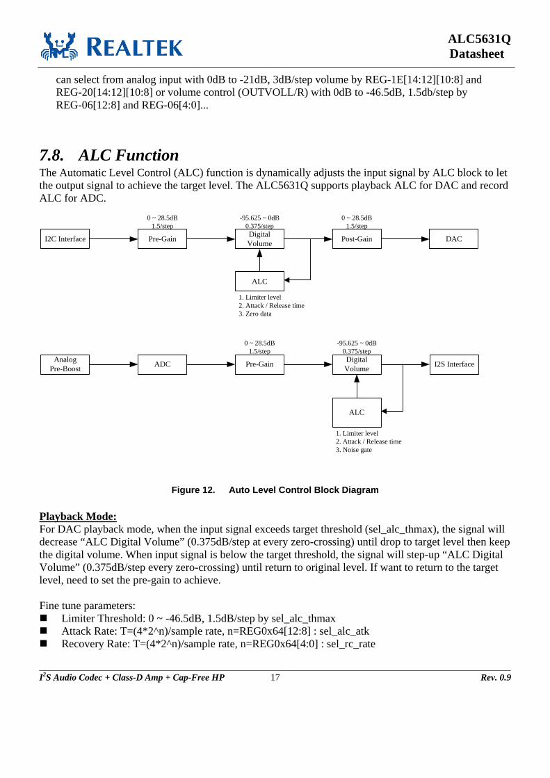
7.8. ALC Function The Automatic Level Control (ALC) function is dynamically adjusts the input signal by ALC block to let the output signal to achieve the target level. The ALC5631Q supports playback ALC for DAC and record ALC for ADC.
I2C Interface Pre-Gain Digital Volume Post-Gain DAC
ALC
-95.625 ~ 0dB 0.375/step
0 ~ 28.5dB1.5/step
0 ~ 28.5dB1.5/step
1. Limiter level2. Attack / Release time3. Zero data
Analog Pre-Boost Pre-Gain Digital
Volume I2S Interface
ALC
-95.625 ~ 0dB 0.375/step
0 ~ 28.5dB1.5/step
1. Limiter level2. Attack / Release time3. Noise gate
ADC
Figure 12. Auto Level Control Block Diagram
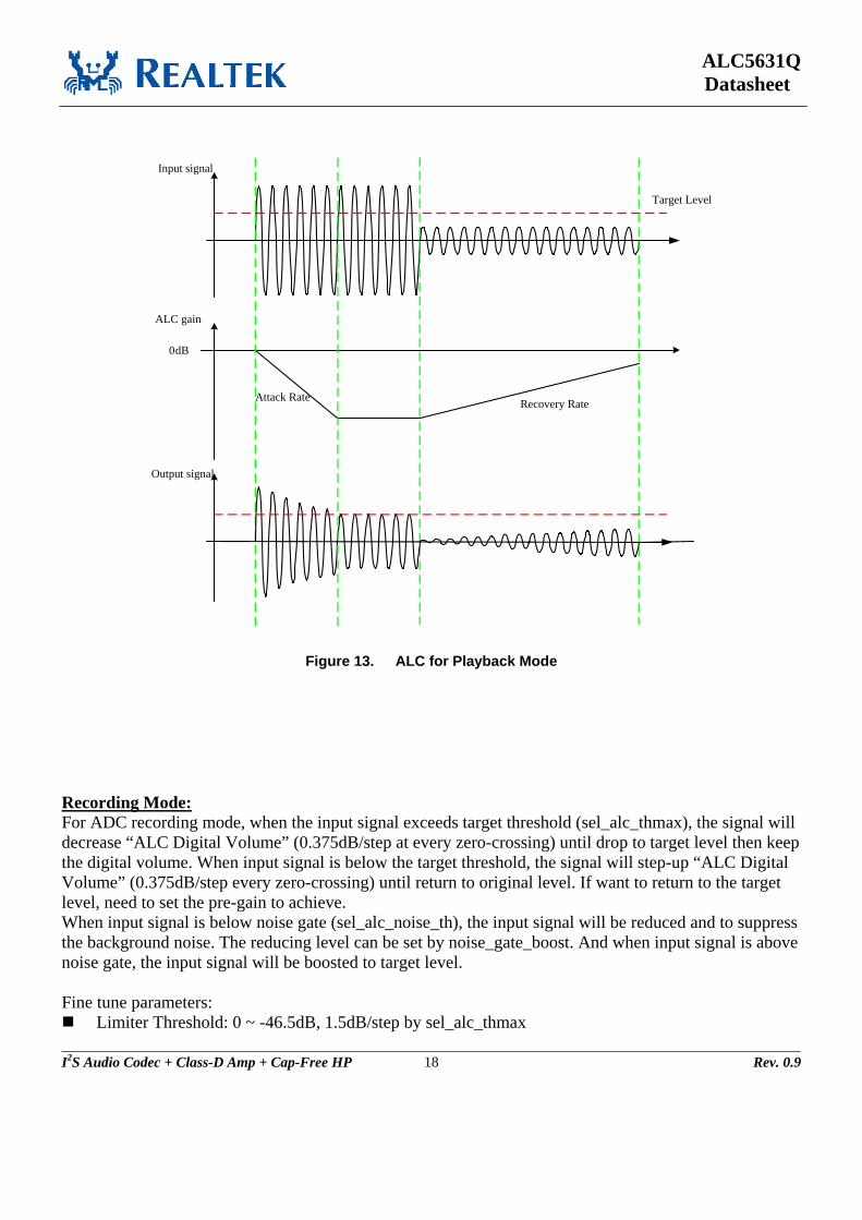
Playback Mode: For DAC playback mode, when the input signal exceeds target threshold (sel_alc_thmax), the signal will decrease “ALC Digital Volume” (0.375dB/step at every zero-crossing) until drop to target level then keep the digital volume. When input signal is below the target threshold, the signal will step-up “ALC Digital Volume” (0.375dB/step every zero-crossing) until return to original level. If want to return to the target level, need to set the pre-gain to achieve. Fine tune parameters:
Limiter Threshold: 0 ~ -46.5dB, 1.5dB/step by sel_alc_thmax Attack Rate: T=(4*2^n)/sample rate, n=REG0x64[12:8] : sel_alc_atk Recovery Rate: T=(4*2^n)/sample rate, n=REG0x64[4:0] : sel_rc_rate
ALC5631Q Datasheet
I2S Audio Codec + Class-D Amp + Cap-Free HP 18 Rev. 0.9
ALC gain
0dB
Input signal
Output signal
Target Level
Attack Rate Recovery Rate
Figure 13. ALC for Playback Mode Recording Mode: For ADC recording mode, when the input signal exceeds target threshold (sel_alc_thmax), the signal will decrease “ALC Digital Volume” (0.375dB/step at every zero-crossing) until drop to target level then keep the digital volume. When input signal is below the target threshold, the signal will step-up “ALC Digital Volume” (0.375dB/step every zero-crossing) until return to original level. If want to return to the target level, need to set the pre-gain to achieve. When input signal is below noise gate (sel_alc_noise_th), the input signal will be reduced and to suppress the background noise. The reducing level can be set by noise_gate_boost. And when input signal is above noise gate, the input signal will be boosted to target level. Fine tune parameters:
Limiter Threshold: 0 ~ -46.5dB, 1.5dB/step by sel_alc_thmax

ALC5631Q Datasheet
I2S Audio Codec + Class-D Amp + Cap-Free HP 19 Rev. 0.9
Attack Rate: T=(4*2^n)/sample rate, n=REG0x64[12:8] : sel_alc_atk Recovery Rate: T=(4*2^n)/sample rate, n=REG0x64[12:8] : sel_rc_rate Noise Gate Threshold: -36 ~ -82.5dB, 1.5dB/step by sel_alc_noise_th Reducing Noise Level: 0 ~ 45dB, 3dB/step by noise_gate_boost
ALC gain
0dB
Input signal
Output signal
Target Level
Attack Rate Recovery Rate
Noise Gate
Attack Rate Recovery Rate
Noise Gate
Target Level
Noise Reduction
Figure 14. ALC for Recording Mode

ALC5631Q Datasheet
I2S Audio Codec + Class-D Amp + Cap-Free HP 20 Rev. 0.9
7.9. Speaker Amplifier Ratio Gain Owing to speaker power (SPKVDD) and analog power (AVDD) is different power domain. And normally the speaker power is higher than analog power. So the audio input signal is need to be boost or reduce by a gain and then output from speaker amplifier. When SPKVDD is dropping, the gain need to be reduced to prevent the signal is clipped. And when SPKVDD is rising, the gain need to be boosted to prevent the signal is to small. en_spk_auto_ratio is used to enable speaker amplifier auto gain ratio.
Table 11. Ration Gain Table for SPKVDD
AVDD = 2.5V AC Ratio Gain Setting Gain ( dB )
5.86 V 2.34 111'b 7.400227 4.99 V 2.00 110'b 5.999729 4.20 V 1.68 101'b 4.506186 3.90 V 1.56 100'b 3.862492 3.60 V 1.44 011'b 3.16725 3.18 V 1.27 010'b 2.1 2.74 V 1.10 001'b 0.8
SPKVDD
2.50 V 1.00 000'b 0
AVDD = 2.5V
SPKVDD = 4.2V
VMID =1.25V
VMID = 2.1V
SPKVDD = 3.6V
VMID = 1.8V
Figure 15. Ratio Gain for SPKVDD and AVDD

ALC5631Q Datasheet
I2S Audio Codec + Class-D Amp + Cap-Free HP 21 Rev. 0.9
7.10. Hardware Sound Processing The Sound Effect block is composed of Pseudo Stereo, Spatial 3D, and Equalizer blocks. The Pseudo Stereo block is used to convert a MONO source into virtualized stereo output. The Spatial 3D block is a surround sound generator with adjustable amplitude (Gain) and surround depth (Ratio). The Equalizer block can be used to compensate for speaker response, or to make environment sound effects, e.g., ‘Pub’, ‘Live’, ‘Rock’,… etc..
7.10.1. Equalizer Block The equalizer block cascades 6 bands of equalizer to compensate for speaker response and to emulate environment sound. The 6 bands equalizer are include two high pass filter, three band pass filter and one low pass filter. One high pass filter cascaded in the front end is used to drop low frequency tone, the tone has a large amplitude and may damage a mini speaker.
The high pass filter can also be used to adjust Treble strength with gain control. One low pass filter with gain control can adjust the Bass strength. Three bands of bi-quad band pass filters are used to emulate environment sounds.
7.10.2. Pseudo Stereo and Spatial 3D Sound There are two spatial effects in post-processing; the Pseudo-Stereo Effect + Spatial Effect, and the Stereo Expansion Effect. The Pseudo-Stereo Effect + Spatial Effect converts a MONO signal to a stereo signal by changing the phase and amplitude of the original signal followed by enhancing the spatial effect. The Stereo Expansion Effect enhances the spatial effect when the input signal is Stereo.
7.10.3. Wind Noise Reduction Filter The wind filter is implemented by a high pass filter equalizer. The wind filter is mainly for ADC recording used. The bandwidth of wind filter is programmable and varies with sample rate. The filter is used to remove DC offset at normal condition, and wind noise reduction at application mode.
Table 12. Sample Rate with bandwidth for Wind Filter Sampling Rate (sel_adhpf_fs_type) = 48kHz sel_adc_wf
00’b 01’b 10’b 000 130 Hz 260 Hz 440 Hz 001 170 Hz 330 Hz 556 Hz 010 171 Hz 330 Hz 556 Hz 011 254 Hz 448 Hz 770 Hz 100 330 Hz 640 Hz 1124 Hz 101 420 Hz 730 Hz 1200 Hz 110 509 Hz 770 Hz 2000 Hz 111 620 Hz 1260 Hz 2155 Hz

ALC5631Q Datasheet
I2S Audio Codec + Class-D Amp + Cap-Free HP 22 Rev. 0.9
7.11. I2C Control Interface I2C is a 2-wire (SCL/SDA) half-duplex serial communication interface, supporting only slave mode. SCL is used for clock and SDA is for data. SCL clock supports up to 400KHz rate and SDA data is a open drain structure. The input has built-in spike filter and can remove less than 50ns spike at SCL and SDA.
7.11.1. Address Setting Table 13. Address Setting (0x34h)
(MSB) BIT (LSB) 0 0 1 1 0 1 0 R/W
7.11.2. Complete Data Transfer Data Transfer over I2C Control Interface
Figure 16. Data Transfer Over I2C Control Interface
Write WORD Protocol Table 1. Write WORD Protocol
Read WORD Protocol Table 2. Read WORD Protocol

ALC5631Q Datasheet
I2S Audio Codec + Class-D Amp + Cap-Free HP 23 Rev. 0.9
S: Start Condition A: 0 for ACK, 1 for NACK
Slave Address: 7-bit Device Address Data Byte: 16-bit Mixer data
Wr: 0 for Write Command : Master-to-Slave
Rd: 1 for Read Command : Slave-to-Master
Command Code: 8-bit Register Address
7.11.3. Odd-Addressed Register Access The ALC5631Q will return ‘0000h’ when odd-addressed and unimplemented registers are read.
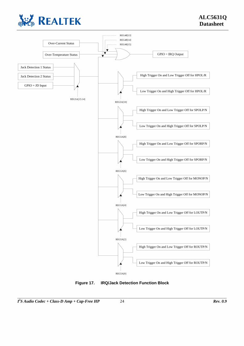
7.12. GPIO, Interrupt and Jack Detection The ALC5631Q supports one GPIO. The GPIO can be configured as Input/Output by REG4C[2]. When GPIO is configured as input, the status will be indicated in REG4A[2]. When GPIO is configured as output, REG4C[1] is used to drive GPIO to high or low.
The GPIO is also can as IRQ output and triggered by trigger sources. The trigger sources can from over-current status, over-temperature status and jack detection. Each of these is trigged and the GPIO will output a flag as interrupt signal.
There are three pins can as jack detect pins, GPIO, JD1 (share with AXIL) and JD2 (share with AXIR). The jack detect function is use to turn-on or turn-off output port. When jack detect pin has been trigged, the selected output ports will be turn-on or turn-off. When GPIO is as IRQ function then will not as jack detect pin.
ALC5631Q Datasheet
I2S Audio Codec + Class-D Amp + Cap-Free HP 24 Rev. 0.9
Over-Current Status
Over-Temperature Status
Jack Detection 1 Status
Jack Detection 2 Status
GPIO = JD Input
GPIO = IRQ Output
High Trigger On and Low Trigger Off for HPOL/R
REG5A[15:14]REG5A[10]
High Trigger On and Low Trigger Off for SPOLP/N
Low Trigger On and High Trigger Off for SPOLP/N
REG5A[8]
REG5A[6]
High Trigger On and Low Trigger Off for MONOP/N
Low Trigger On and High Trigger Off for MONOP/N
REG5A[4]
High Trigger On and Low Trigger Off for LOUTP/N
Low Trigger On and High Trigger Off for LOUTP/N
REG5A[2]
High Trigger On and Low Trigger Off for ROUTP/N
Low Trigger On and High Trigger Off for ROUTP/N
REG5A[0]
REG48[15]
REG48[14]
REG48[13]
Low Trigger On and High Trigger Off for HPOL/R
High Trigger On and Low Trigger Off for SPORP/N
Low Trigger On and High Trigger Off for SPORP/N
Figure 17. IRQ/Jack Detection Function Block

ALC5631Q Datasheet
I2S Audio Codec + Class-D Amp + Cap-Free HP 25 Rev. 0.9
7.13. Power Management ALC5631Q detailed Power Management control registers are supported in Reg3A, 3B, 3C, 3E. Each particular block will only be active when individual bits of Reg3A are set to enable.

ALC5631Q Datasheet
I2S Audio Codec + Class-D Amp + Cap-Free HP 26 Rev. 0.5
8. Registers List Accessing odd numbered registers, or reading unimplemented registers, will return a 0.
8.1. Reg-00h: Reset Default: 0001’h
Table 14. Reg-00h: Reset Port Name Bits Read/Write Reset State Description Reserved 15:4 - 0’h Reserved Reg-00_b3 3 R 0’h Internal used Reg-00_b2 2 R 0’h Internal used Reg-00_b1 1 R 0’h Internal used Reg-00_b0 0 R 1’h Internal used Note: Writes to this register will reset all registers to their default values except PLL related Register. The written data will be ignored.
8.2. Reg-02h: Speaker Output Control Default: 8888’h
Table 15. Reg-02h: Speaker Output Control Port Name Bits Read/Write Reset State Description mu_spo_l 15 R/W 1’h Mute Control for SPOLP/LN
0’b: Un-mute 1’b: Mute
sel_spkvoll_in 14 R/W 0’h Speaker Left Channel Volume Input Select 0’b: VMID (No input) 1’b: SPKMIXL
vol_spo_l 13:8 R/W 8’h Speaker Left Channel Volume Control (SPKVOLL) 00’h: +12dB ~ 08’h: 0dB ~ 27’h: -46.5dB, with 1.5dB/step
mu_spo_r 7 R/W 1’h Mute Control for SPO_RP/RN 0’b: Un-mute 1’b: Mute
sel_spkvolr_in 6 R/W 0’h Speaker Right Channel Volume Input Select 0’b: VMID (No input) 1’b: SPKMIXR

ALC5631Q Datasheet
I2S Audio Codec + Class-D Amp + Cap-Free HP 27 Rev. 0.9
Port Name Bits Read/Write Reset State Description vol_spo_r 5:0 R/W 8’h Speaker Right Channel Volume Control (SPKVOLR)
00’h: +12dB ~ 08’h: 0dB ~ 27’h: -46.5dB, with 1.5dB/step
8.3. Reg-04h: Headphone Output Control Default: 8080’h
Table 16. Reg-04h: Headphone Output Control Name Bits Read/Write Reset State Description mu_hpo_l 15 R/W 1’h Mute Control for HPOL
0’b: Un-mute 1’b: Mute
sel_hpovoll_in 14 R/W 0’h Headphone Left Channel Volume Input Select 0’b: VMID (No input) 1’b: OUTMIXL
Reserved 13 - 0’h Reserved vol_hpo_l 12:8 R/W 0’h Headphone Left Channel Volume Control (HPOVOLL)
00’h: 0dB ~ 1F’h: -46.5dB, with 1.5dB/step
mu_hpo_r 7 R/W 1’h Mute Control for HPOR 0’b: Un-mute 1’b: Mute
sel_hpovolr_in 6 R/W 0’h Headphone Right Channel Volume Input Select 0’b: VMID (No input) 1’b: OUTMIXR
Reserved 5 - 0’h Reserved vol_hpo_r 4:0 R/W 0’h Headphone Right Channel Volume Control (HPOVOLR)
00’h: 0dB ~ 1F’h: -46.5dB, with 1.5dB/step
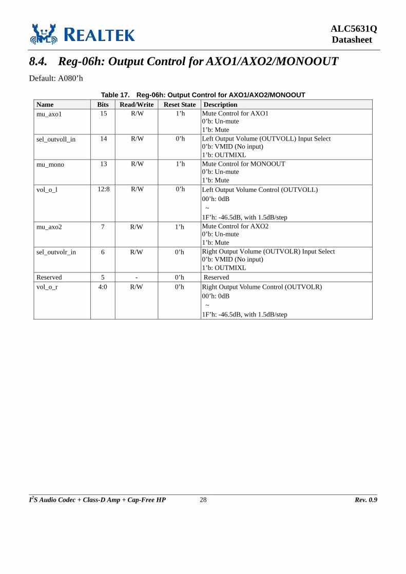
ALC5631Q Datasheet
I2S Audio Codec + Class-D Amp + Cap-Free HP 28 Rev. 0.9
8.4. Reg-06h: Output Control for AXO1/AXO2/MONOOUT Default: A080’h
Table 17. Reg-06h: Output Control for AXO1/AXO2/MONOOUT Name Bits Read/Write Reset State Description mu_axo1 15 R/W 1’h Mute Control for AXO1
0’b: Un-mute 1’b: Mute
sel_outvoll_in 14 R/W 0’h Left Output Volume (OUTVOLL) Input Select 0’b: VMID (No input) 1’b: OUTMIXL
mu_mono 13 R/W 1’h Mute Control for MONOOUT 0’b: Un-mute 1’b: Mute
vol_o_l 12:8 R/W 0’h Left Output Volume Control (OUTVOLL) 00’h: 0dB ~ 1F’h: -46.5dB, with 1.5dB/step
mu_axo2 7 R/W 1’h Mute Control for AXO2 0’b: Un-mute 1’b: Mute
sel_outvolr_in 6 R/W 0’h Right Output Volume (OUTVOLR) Input Select 0’b: VMID (No input) 1’b: OUTMIXL
Reserved 5 - 0’h Reserved vol_o_r 4:0 R/W 0’h Right Output Volume Control (OUTVOLR)
00’h: 0dB ~ 1F’h: -46.5dB, with 1.5dB/step

ALC5631Q Datasheet
I2S Audio Codec + Class-D Amp + Cap-Free HP 29 Rev. 0.9
8.5. Reg-0Ah: AUX INPUT Volume Control Default: 0808’h
Table 18. Reg-0Ah: AUX INPUT Volume Control Name Bits Read/Write Reset State Description Reserved 15:13 - 0’h Reserved vol_axi_l 12:8 R/W 8’h AUX Left Input Volume Control
00’h: 12dB ~ 08’h: 0dB ~ 1F’h: -34.5dB, with 1.5dB/step
Reserved 7:5 - 0’h Reserved vol_axi_r 4:0 R/W 8’h AUX Right Input Volume Control
00’h: 12dB ~ 08’h: 0dB ~ 1F’h: -34.5dB, with 1.5dB/step
8.6. Reg-0Ch: STEREO DAC Control 1 Default: 0000’h
Table 19. Reg-0Ch: STEREO DAC Control 1 Name Bits Read/Write Reset State Description mu_dac_l 15 R/W 0’h Digital Mute for Left DAC
0’b: Un-mute 1’b: Mute
Reserved 14:8 R 0’h Reserved mu_dac_r 7 R/W 0’h Digital Mute for Right DAC
0’b: Un-mute 1’b: Mute
sel_dac_pre_bst 6:0 R/W 0’h Digital Pre-Boost Gain 00’h= 0dB 01’h= 0.375dB 02’h= 0.75dB 03’h= 1.125dB ~ 4C’h= 28.5dB, with 0.375dB/step Others: Reserved

ALC5631Q Datasheet
I2S Audio Codec + Class-D Amp + Cap-Free HP 30 Rev. 0.9
8.7. Reg-0Eh: Microphone Input Control Default: 0000’h
Table 20. Reg-0Eh: Microphone Input Control Name Bits Read/Write Reset State Description en_mic1_df 15 R/W 0’h MIC1 Input Mode Control
0’b: Single-ended input (Input is from MIC1N) 1’b: Differential input
Reserved 14:8 - 0’h Reserved en_mic2_df 7 R/W 0’h MIC2 Input Mode Control
0’b: Single-ended input (Input is from MIC2N) 1’b: Differential input
Reserved 6:0 - 0’h Reserved
8.8. Reg-10h: STEREO DAC Control 2 Default: 0000’h
Table 21. Reg-10h: STEREO DAC Control 2 Name Bits Read/Write Reset State Description vol_dac_l 15:8 R/W 0’h Stereo DAC Left Channel Digital Volume
00’h: 0dB ~ FF’h: -95.625dB, with 0.375dB/step
vol_dac_r 7:0 R/W 0’h Stereo DAC Right Channel Digital Volume 00’h: 0dB ~ FF’h: -95.625dB, with 0.375dB/step
8.9. Reg-12h: Stereo ADC Control 1 Default: 0000’h
Table 22. Reg-12h: Stereo ADC Control 1 Name Bits Read/Write Reset State Description mu_adc_l 15 R/W 0’h Digital Mute for Left ADC
0’b: Un-mute 1’b: Mute
Reserved 14:8 - 0’h Reserved mu_adc_r 7 R/W 0’h Digital Mute for Right ADC
0’b: Un-mute 1’b: Mute
Reserved 6:5 - 0’h Reserved

ALC5631Q Datasheet
I2S Audio Codec + Class-D Amp + Cap-Free HP 31 Rev. 0.9
Name Bits Read/Write Reset State Description sel_adc_pre_bst 4:0 R/W 0’h Digital Pre-Boost Gain
00’h= 0dB 01’h= 1.5dB 02’h= 3dB 03’h= 4.5dB ……………….. 13’h= 28.5dB, with 1.5dB/step Others: Reserved
8.10. Reg-14h: ADC Recording Mixer Control Default: F0F0’h
Table 23. Reg-14h: ADC Recording Mixer Control Name Bits Read/Write Reset State Description mu_outmixl_to_recmixl
15 R/W 1’h Left Output Mixer (OUTMIXL) to Left REC Mixer (RECMIXL) 0’b: Un-mute 1’b: Mute
mu_bst1_to_recmixl 14 R/W 1’h MIC1 to Left REC Mixer (RECMIXL) 0’b: Un-mute 1’b: Mute
mu_axilvol_to_recmixl
13 R/W 1’h AXIL to Left REC Mixer (RECMIXL) 0’b: Un-mute 1’b: Mute
mu_rx_to_recmixl 12 R/W 1’h MONOIN to Left REC Mixer (RECMIXL) 0’b: Un-mute 1’b: Mute
reserved 11:8 - 0’h Reserved mu_outmixr_to_recmixr
7 R/W 1’h Right Output Mixer (OUTMIXR) to Right REC Mixer (RECMIXR)
0’b: Un-mute
1’b: Mute mu_bst2_to_recmixr 6 R/W 1’h MIC2 to Right REC Mixer (RECMIXR)
0’b: Un-mute
1’b: Mute mu_axirvol_to_recmixr
5 R/W 1’h AXIR to Right REC Mixer (RECMIXR)
0’b: Un-mute
1’b:Mute mu_rx_to_recmixr 4 R/W 1’h MONOIN to Right REC Mixer (RECMIXR)
0’b: Un-mute
1’b: Mute reserved 3:0 - 0’h Reserved

ALC5631Q Datasheet
I2S Audio Codec + Class-D Amp + Cap-Free HP 32 Rev. 0.9
8.11. Reg-16h: Stereo ADC Control 2 Default: 0000’h
Table 24. Reg-16h: Stereo ADC Control 2 Name Bits Read/Write Reset State Description vol_adc_l 15:8 R/W 0’h Stereo ADC Left Channel Digital Volume
00’h: 0dB ~ FF’h: -95.625dB, with 0.375dB/step
vol_adc_r 7:0 R/W 0’h Stereo ADC Right Channel Digital Volume 00’h: 0dB ~ FF’h: -95.625dB, with 0.375dB/step
8.12. Reg-1Ah: Left Output Mixer (OUTMIXL) Control Default: FFC0’h
Table 25. Reg-1Ah: Left Output Mixer Control Name Bits Read/Write Reset State Description mu_recmixl_to_outmixl
15 R/W 1’h Left REC Mixer (RECMIXL) to Left Output Mixer (OUTMIXL) 0’b: Un-mute 1’b: Mute
mu_recmixr_to_outmixl
14 R/W 1’h Right REC Mixer (RECMIXR) to Left Output Mixer (OUTMIXL) 0’b: Un-mute 1’b: Mute
mu_dacl_to_outmixl 13 R/W 1’h Left DAC Output to Left Output Mixer (OUTMIXL) 0’b: Un-mute 1’b: Mute
mu_bst1_to_outmixl 12 R/W 1’h MIC1 to Left Output Mixer (OUTMIXL) 0’b: Un-mute 1’b: Mute
mu_bst2_to_outmixl 11 R/W 1’h MIC2 to Left Output Mixer (OUTMIXL)
0’b: Un-mute 1’b: Mute
mu_rxn_to_outmixl 10 R/W 1’h MONOIN Negative Input to Left Output Mixer (OUTMIXL)
0’b: Un-mute 1’b: Mute
mu_axilvol_to_outmixl
9 R/W 1’h AXIL to Left Output Mixer (OUTMIXL) 0’b: Un-mute 1’b: Mute
mu_axirvol_to_outmixl
8 R/W 1’h AXIR to Left Output Mixer (OUTMIXL) 0’b: Un-mute 1’b: Mute
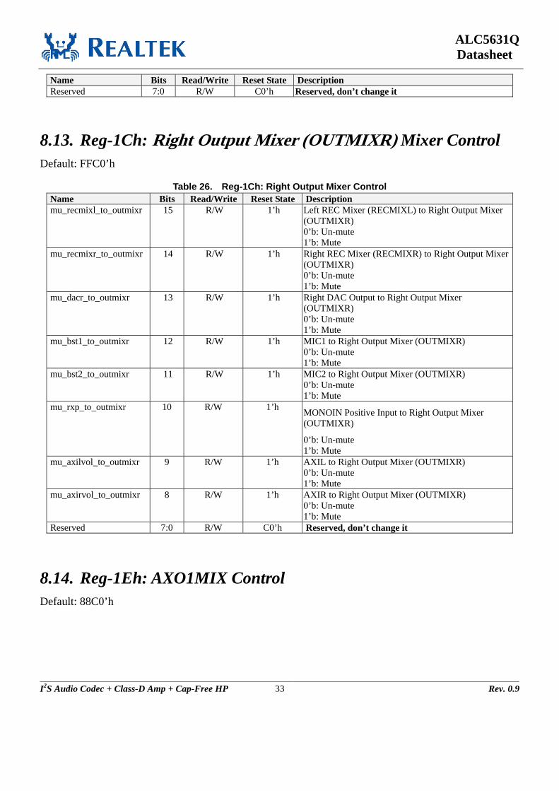
ALC5631Q Datasheet
I2S Audio Codec + Class-D Amp + Cap-Free HP 33 Rev. 0.9
Name Bits Read/Write Reset State Description Reserved 7:0 R/W C0’h Reserved, don’t change it
8.13. Reg-1Ch: Right Output Mixer (OUTMIXR) Mixer Control Default: FFC0’h
Table 26. Reg-1Ch: Right Output Mixer Control Name Bits Read/Write Reset State Description mu_recmixl_to_outmixr 15 R/W 1’h Left REC Mixer (RECMIXL) to Right Output Mixer
(OUTMIXR) 0’b: Un-mute 1’b: Mute
mu_recmixr_to_outmixr 14 R/W 1’h Right REC Mixer (RECMIXR) to Right Output Mixer (OUTMIXR) 0’b: Un-mute 1’b: Mute
mu_dacr_to_outmixr 13 R/W 1’h Right DAC Output to Right Output Mixer (OUTMIXR) 0’b: Un-mute 1’b: Mute
mu_bst1_to_outmixr 12 R/W 1’h MIC1 to Right Output Mixer (OUTMIXR) 0’b: Un-mute 1’b: Mute
mu_bst2_to_outmixr 11 R/W 1’h MIC2 to Right Output Mixer (OUTMIXR) 0’b: Un-mute 1’b: Mute
mu_rxp_to_outmixr 10 R/W 1’h MONOIN Positive Input to Right Output Mixer (OUTMIXR)
0’b: Un-mute 1’b: Mute
mu_axilvol_to_outmixr 9 R/W 1’h AXIL to Right Output Mixer (OUTMIXR) 0’b: Un-mute 1’b: Mute
mu_axirvol_to_outmixr 8 R/W 1’h AXIR to Right Output Mixer (OUTMIXR) 0’b: Un-mute 1’b: Mute
Reserved 7:0 R/W C0’h Reserved, don’t change it
8.14. Reg-1Eh: AXO1MIX Control Default: 88C0’h
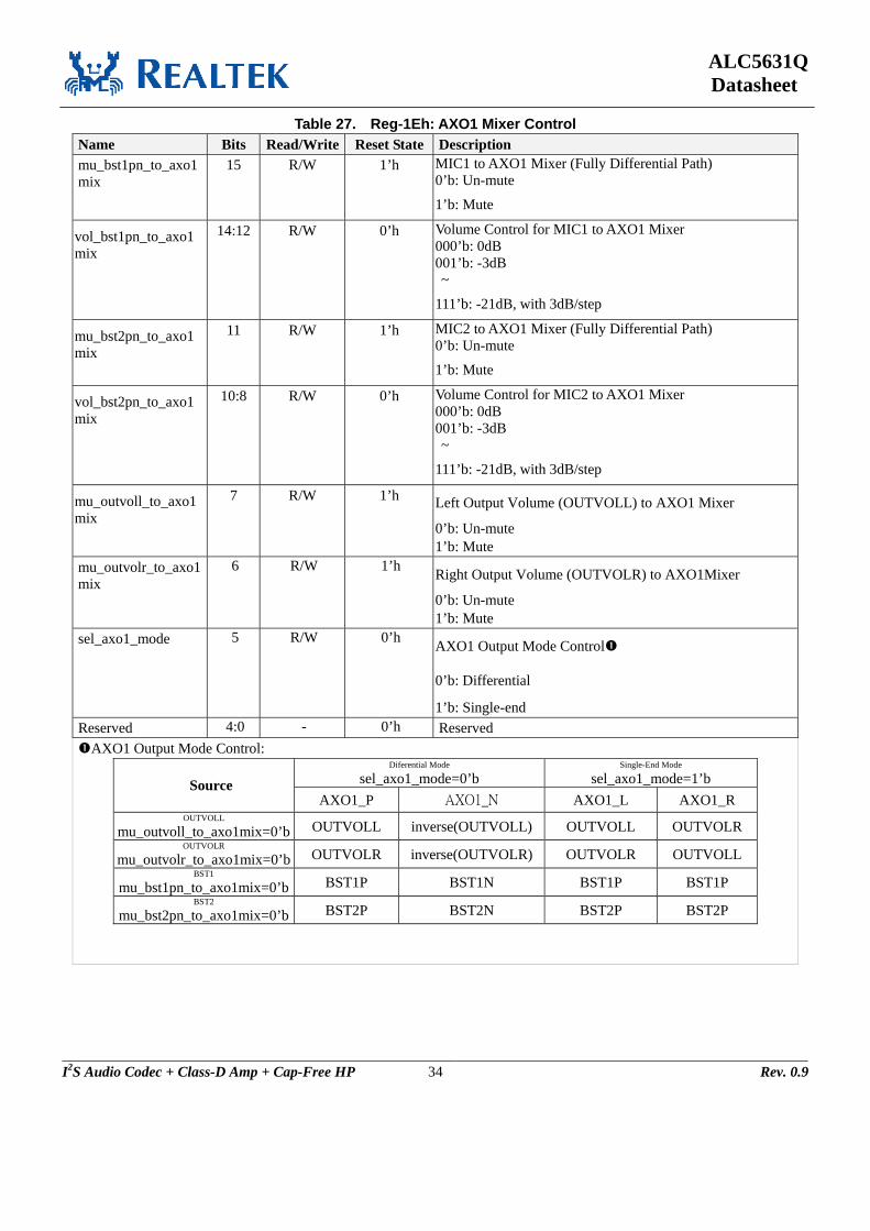
ALC5631Q Datasheet
I2S Audio Codec + Class-D Amp + Cap-Free HP 34 Rev. 0.9
Table 27. Reg-1Eh: AXO1 Mixer Control Name Bits Read/Write Reset State Description mu_bst1pn_to_axo1mix
15 R/W 1’h MIC1 to AXO1 Mixer (Fully Differential Path) 0’b: Un-mute
1’b: Mute
vol_bst1pn_to_axo1mix
14:12 R/W 0’h Volume Control for MIC1 to AXO1 Mixer 000’b: 0dB 001’b: -3dB ~
111’b: -21dB, with 3dB/step
mu_bst2pn_to_axo1mix
11 R/W 1’h MIC2 to AXO1 Mixer (Fully Differential Path) 0’b: Un-mute
1’b: Mute
vol_bst2pn_to_axo1mix
10:8 R/W 0’h Volume Control for MIC2 to AXO1 Mixer 000’b: 0dB 001’b: -3dB ~
111’b: -21dB, with 3dB/step
mu_outvoll_to_axo1mix
7 R/W 1’h Left Output Volume (OUTVOLL) to AXO1 Mixer
0’b: Un-mute 1’b: Mute
mu_outvolr_to_axo1mix
6 R/W 1’h Right Output Volume (OUTVOLR) to AXO1Mixer
0’b: Un-mute 1’b: Mute
sel_axo1_mode 5 R/W 0’h AXO1 Output Mode Control
0’b: Differential
1’b: Single-end Reserved 4:0 - 0’h Reserved
AXO1 Output Mode Control: Diferential Mode
sel_axo1_mode=0’b Single-End Mode
sel_axo1_mode=1’b Source AXO1_P AXO1_N AXO1_L AXO1_R
OUTVOLL
mu_outvoll_to_axo1mix=0’b OUTVOLL inverse(OUTVOLL) OUTVOLL OUTVOLR OUTVOLR
mu_outvolr_to_axo1mix=0’b OUTVOLR inverse(OUTVOLR) OUTVOLR OUTVOLL BST1
mu_bst1pn_to_axo1mix=0’b BST1P BST1N BST1P BST1P BST2
mu_bst2pn_to_axo1mix=0’b BST2P BST2N BST2P BST2P
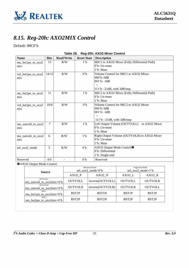
ALC5631Q Datasheet
I2S Audio Codec + Class-D Amp + Cap-Free HP 35 Rev. 0.9
8.15. Reg-20h: AXO2MIX Control Default: 88C0’h
Table 28. Reg-20h: AXO2 Mixer Control Name Bits Read/Write Reset State Description mu_bst1pn_to_axo2mix
15 R/W 1’h MIC1 to AXO2 Mixer (Fully Differential Path) 0’b: Un-mute 1’b: Mute
vol_bst1pn_to_axo2mix
14:12 R/W 0’h Volume Control for MIC1 to AXO2 Mixer 000’b: 0dB 001’b: -3dB ~ 111’b: -21dB, with 3dB/step
mu_bst2pn_to_axo2mix
11 R/W 1’h MIC2 to AXO2 Mixer (Fully Differential Path) 0’b: Un-mute 1’b: Mute
vol_bst2pn_to_axo2mix
10:8 R/W 0’h Volume Control for MIC2 to AXO2 Mixer 000’b: 0dB 001’b: -3dB ~ 111’b: -21dB, with 3dB/step
mu_outvoll_to_axo2mix
7 R/W 1’h Left Output Volume (OUTVOLL) to AXO2 Mixer 0’b: Un-mute 1’b: Mute
mu_outvolr_to_axo2mix
6 R/W 1’h Right Output Volume (OUTVOLR) to AXO2 Mixer 0’b: Un-mute 1’b: Mute
sel_axo2_mode 5 R/W 0’h AXO2 Output Mode Control 0’b: Differential 1’b: Single-end
Reserved 4:0 - 0’h Reserved AXO2 Output Mode Control:
Diferential Mode
sel_axo2_mode=0’b Single-End Mode
sel_axo2_mode=1’b Source AXO2_P AXO2_N AXO2_L AXO2_R
OUTVOLL
mu_outvoll_to_axo2mix=0’b OUTVOLL inverse(OUTVOLL) OUTVOLL OUTVOLR OUTVOLR
mu_outvolr_to_axo2mix=0’b OUTVOLR inverse(OUTVOLR) OUTVOLR OUTVOLL BST1
mu_bst1pn_to_axo2mix=0’b BST1P BST1N BST1P BST1P BST2
mu_bst2pn_to_axo2mix=0’b BST2P BST2N BST2P BST2P

ALC5631Q Datasheet
I2S Audio Codec + Class-D Amp + Cap-Free HP 36 Rev. 0.9
8.16. Reg-22h: Microphone Input Control Default: 0000’h
Table 29. Reg-22h: Microphone Input Control Name Bits Read/Write Reset State Description sel_bst1 15:12 R/W 0’h MIC1 Input Boost Gain Control
0000’b: Bypass 0001’b: +20dB 0010’b: +24dB 0011’b: +30dB 0100’b: +35dB 0101’b: +40dB 0110’b: +44dB 0111’b: +50dB 1000’b: +52dB Others : Reserved
sel_bst2 11:8 R/W 0’h MIC2 Input Boost Gain Control 0000’b: Bypass 0001’b: +20dB 0010’b: +24dB 0011’b: +30dB 0100’b: +35dB 0101’b: +40dB 0110’b: +44dB 0111’b: +50dB 1000’b: +52dB Others : Reserved
sel_micbias1 7 R/W 0’h MICBIAS1 Output Voltage Control 0’b: 0.9 * AVDD
1’b: 0.75 * AVDD
pow_mic_ovcd1 6 R/W 0’h MICBIAS1 Short Current Detector Control 0’b: Disable
1’b: Enable
sel_mic_ovcd_th1 5:4 R/W 0’h MICBIAS1 Short Current Detector Threshold 00’b: 600uA 01’b: 1500uA 1x’b: 2000uA Note: tolerance is 200uA

ALC5631Q Datasheet
I2S Audio Codec + Class-D Amp + Cap-Free HP 37 Rev. 0.9
Name Bits Read/Write Reset State Description sel_micbias2 3 R/W 0’h MICBIAS2 Output Voltage Control
0’b: 0.9 * AVDD 1’b: 0.75 * AVDD
pow_mic_ovcd2 2 R/W 0’h MICBIAS2 Short Current Detector Control 0’b: Disable 1’b: Enable
sel_mic_ovcd_th2 1:0 R/W 0’h MICBIAS2 Short Current Detector Threshold 00’b: 600uA 01’b: 1500uA 1x’b: 2000uA Note: tolerance is 200uA
8.17. Reg-24h: Digital Microphone Control Default: 3000’h
Table 30. Reg-24h: Digital Microphone Control Name Bits Read/Write Reset State Description en_dmic 15 R/W 0’h Enable DMIC Interface(ADC digital MUX selection)
0’b: Disable (ADC to ADC Digital Filter) 1’b: Enable (DMIC to ADC Digital Filter)
Reserved 14 - 0’h Reserved mu_dmic_l 13 R/W 1’h DMIC Left Channel Mute Control
0’b: Un-mute 1’b: Mute
mu_dmic_r 12 R/W 1’h DMIC Right Channel Mute Control 0’b: Un-mute 1’b: Mute
Reserved 11:10 - 0’h Reserved
sel_dmic_l_edge 9 R/W 0’h DMIC Left Channel Source Control 0’b: Latch from falling edge
1’b: Latch from rising edge
sel_dmic_r_edge 8 R/W 0’h DMIC ADC Right Channel Source Control 0’b: Latch from falling edge
1’b: Latch from rising edge
Reserved 7:6 - 0’h Reserved
sel_dmic_clk 5:4 R/W 0’h DMIC Clock Rate Control 00’b: 128*fs 01’b: 64*fs 1x’b: 32*fs
Reserved 3:0 - 0’h Reserved

ALC5631Q Datasheet
I2S Audio Codec + Class-D Amp + Cap-Free HP 38 Rev. 0.9
8.18. Reg-26h: MONOIN Input Volume Default: 8808’h
Table 31. Reg-26h: MONOIN Input Volume Name Bits Read/Write Reset State Description en_rx_df 15 R/W 1’h MONOIN Input Mode Control
0’b: Single-ended input
1’b: Differential input
Reserved 14:13 - 0’h Reserved
vol_rx_p 12:8 R/W 8’h MONOIN_N Input Volume Control
00’h: 12dB ~ 08’h: 0dB ~
1F’h: -34.5dB, with 1.5dB/step
Reserved 7:5 - 0’h Reserved
vol_rx_n 4:0 R/W 8’h MONOIN_P Input Volume Control
00’h: 12dB ~ 08’h: 0dB ~
1F’h: -34.5dB, with 1.5dB/step
8.19. Reg-28h: Speaker Mixer Control Default: F8F8’h
Table 32. Reg-28h: Speaker Mixer Control Name Bits Read/Write Reset State Description mu_recmixl_to_spkmixl
15 R/W 1’h Left REC Mixer (RECMIXL) to Left Speaker Mixer (SPKMIXL) 0’b: Un-mute 1’b: Mute

ALC5631Q Datasheet
I2S Audio Codec + Class-D Amp + Cap-Free HP 39 Rev. 0.9
Name Bits Read/Write Reset State Description mu_mic1p_to_spkmixl
14 R/W 1’h MIC1 Positive Channel to Left Speaker Mixer (SPKMIXL)0’b: Un-mute 1’b: Mute
mu_dacl_to_spkmixl 13 R/W 1’h DAC Left Channel to Left Speaker Mixer (SPKMIXL) 0’b: Un-mute 1’b: Mute
mu_outmixl_to_spkmixl
12 R/W 1’h Left Output Mixer (OUTMIXL) to Left Speaker Mixer (SPKMIXL) 0’b: Un-mute 1’b: Mute
Reserved 11:8 R/W 8’h Reserved, don’t change it
mu_recmixr_to_spkmixr
7 R/W 1’h Right REC Mixer (RECMIXR) to Right Speaker Mixer (SPKMIXR) 0’b: Un-mute 1’b: Mute
mu_mic2p_to_spkmixr
6 R/W 1’h MIC2 Positive Channel to Right Speaker Mixer (SPKMIXR) 0’b: Un-mute 1’b: Mute
mu_dacr_to_spkmixr
5 R/W 1’h DAC Right Channel to Right Speaker Mixer (SPKMIXR) 0’b: Un-mute 1’b: Mute
mu_outmixr_to_spkmixr
4 R/W 1’h Right Output Mixer (OUTMIXR) to Right Speaker Mixer (SPKMIXR) 0’b: Un-mute 1’b: Mute
Reserved 3:0 R/W 8’h Reserved, don’t change it
8.20. Reg-2Ah: Speaker/Mono Output Control Default: FC00’h
Table 33. Reg-2Ah: Speaker/Mono Output Control Name Bits Read/Write Reset State Description mu_spkvoll_to_spolmix
15 R/W 1’h Left Speaker Volume (SPKLVOL) to Left Speaker Output Mixer (SPOLMIX)
0’b: Un-mute 1’b: Mute
mu_spkvolr_to_spolmix
14 R/W 1’h Right Speaker Volume (SPKRVOL) to Left Speaker Output Mixer (SPOLMIX)
0’b: Un-mute 1’b: Mute
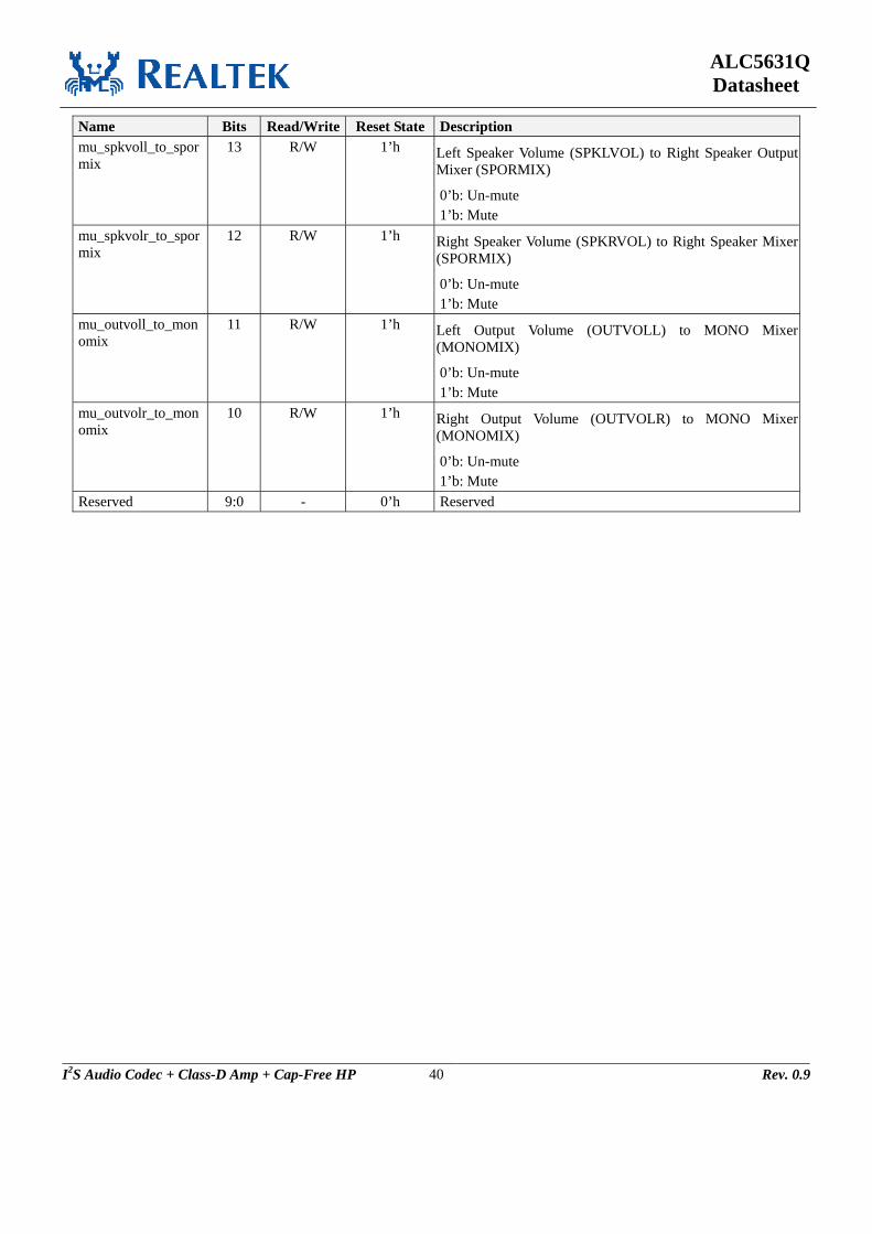
ALC5631Q Datasheet
I2S Audio Codec + Class-D Amp + Cap-Free HP 40 Rev. 0.9
Name Bits Read/Write Reset State Description mu_spkvoll_to_spormix
13 R/W 1’h Left Speaker Volume (SPKLVOL) to Right Speaker Output Mixer (SPORMIX)
0’b: Un-mute 1’b: Mute
mu_spkvolr_to_spormix
12 R/W 1’h Right Speaker Volume (SPKRVOL) to Right Speaker Mixer (SPORMIX)
0’b: Un-mute 1’b: Mute
mu_outvoll_to_monomix
11 R/W 1’h Left Output Volume (OUTVOLL) to MONO Mixer (MONOMIX)
0’b: Un-mute 1’b: Mute
mu_outvolr_to_monomix
10 R/W 1’h Right Output Volume (OUTVOLR) to MONO Mixer (MONOMIX)
0’b: Un-mute 1’b: Mute
Reserved 9:0 - 0’h Reserved

ALC5631Q Datasheet
I2S Audio Codec + Class-D Amp + Cap-Free HP 41 Rev. 0.9
8.21. Reg-2Ch: Speaker/Mono/HP Output Control Default: 4400h
Table 34. Reg-2Ch: Speaker/Mono/HP Output Control Name Bits Read/Write Reset State Description sel_spol 15:14 R/W 1’h Left Speaker Output MUX Selection
00’b: Left Speaker Output Mixer (SPOLMIX) 01’b: MONOIN Input 10’b:Reserved 11’b: DAC Left Channel
Reserved 13:12 - 0’h Reserved sel_spor 11:10 R/W 1’h Right Speaker Output MUX Selection
00’b: Right Speaker Output Mixer (SPORMIX) 01’b: MONOIN Input 10’b: Reserved 11’b: DAC Right Channel
Reserved 9:8 - 0’h Reserved sel_mono 7:6 R/W 1’h Mono Output MUX Selection
00’b: MONO Mixer (MONOMIX) 01’b: MONOIN Input 10’b: Reserved 11’b: Reserved
Reserved 5:4 - 0’h Reserved sel_lin_hp 3 R/W 0’h Left Headphone Output MUX Selection
0’b: Left Headphone Output Volume 1’b: DAC Left Channel
sel_rin_hp 2 R/W 0’h Right Headphone Output MUX Selection 0’b: Right Headphone Output Volume 1’b: DAC Right Channel
Reserved 1:0 - 0’h Reserved

ALC5631Q Datasheet
I2S Audio Codec + Class-D Amp + Cap-Free HP 42 Rev. 0.9
8.22. Reg-34h: Stereo I2S Serial Data Port Control Default: 8000’h
Table 35. Reg-34h: Stereo I2S Serial Data Port Control Name Bits Read/Write Reset State Description sel_i2s_ms 15 R/W 1’h Stereo I2S Serial Data Port Mode Selection
0’b: Master 1’b: Slave
Reserved 14:12 - 0’h Reserved en_adc_comp 11:10 R/W 0’h ADC Compress (For ADCDAT Output)
00’b: OFF 01’b: µ law 10’b: A law 11’b: Reserved
en_dac_comp 9:8 R/W 0’h DAC Compress (For DACDAT Input) 00’b: OFF 01’b: µ law 10’b: A law 11’b: Reserved
inv_bclk 7 R/W 0’h Stereo I2S BCLK Polarity Control 0’b: Normal 1’b: Invert
inv_r_ch 6 R/W 0’h Inverse DAC R Channel Digital Data for Support Differential Output. 0’b: Normal 1’b: Inverse
inv_adc_lrck 5 R/W 0’h ADC Data L/R Swap Control 0’b: ADC data appear at left phase of LRCK 1’b: ADC data appear at right phase of LRCK Note: support to I2S & PCM
inv_dac_lrck 4 R/W 0’h DAC Data L/R Swap Control 0’b: DAC data appear at left phase of LRCK 1’b: DAC data appear at right phase of LRCK Note: support to I2S & PCM
sel_i2s_len 3:2 R/W 0’h Data Length Selection 00’b: 16 bits 01’b: 20 bits 10’b: 24 bits 11’b: 8 bits
sel_i2s_format 1:0 R/W 0’h Stereo PCM Data Format Selection 00’b: I2S format 01’b: Left justified 10’b: PCM mode A 11’b: PCM mode B

ALC5631Q Datasheet
I2S Audio Codec + Class-D Amp + Cap-Free HP 43 Rev. 0.9
8.23. Reg-38h: Stereo ADC/DAC Clock Control Default: 2020’h
Table 36. Reg-38h: Stereo ADC/DAC Clock Control Name Bits Read/Write Reset State Description sel_i2s_pre_div1 15:13 R/W 1’h I2S Pre Div1
000’b: ÷ 1 001’b: ÷ 2 010’b: ÷ 4 011’b: ÷ 8 100’b: ÷ 16 101’b: ÷ 32 Others: Reserved
sel_i2s_bclk_ms1 12 R/W 0’h Master Mode Clock Relative of BCLK and LRCK 0’b: 32Bits (64FS) 1’b: 16Bits (32FS)
sel_dac_osr 11:10 R/W 0’h Stereo DAC Over Sample Rate Select 00’b: 128Fs 01’b: 64Fs 10’b: 32Fs 11’b: 16Fs
sel_adc_osr 9:8 R/W 0’h Stereo ADC Over Sample Rate Select 00’b: 128Fs 01’b: 64Fs 10’b: 32Fs 11’b: 16Fs
sel_filter_clk1 7 R/W 0’h Stereo ADC/DAC Filter Clock Select 0’b: 256Fs 1’b: 384Fs
Reserved 6:0 R/W 2’h Reserved, don’t change it
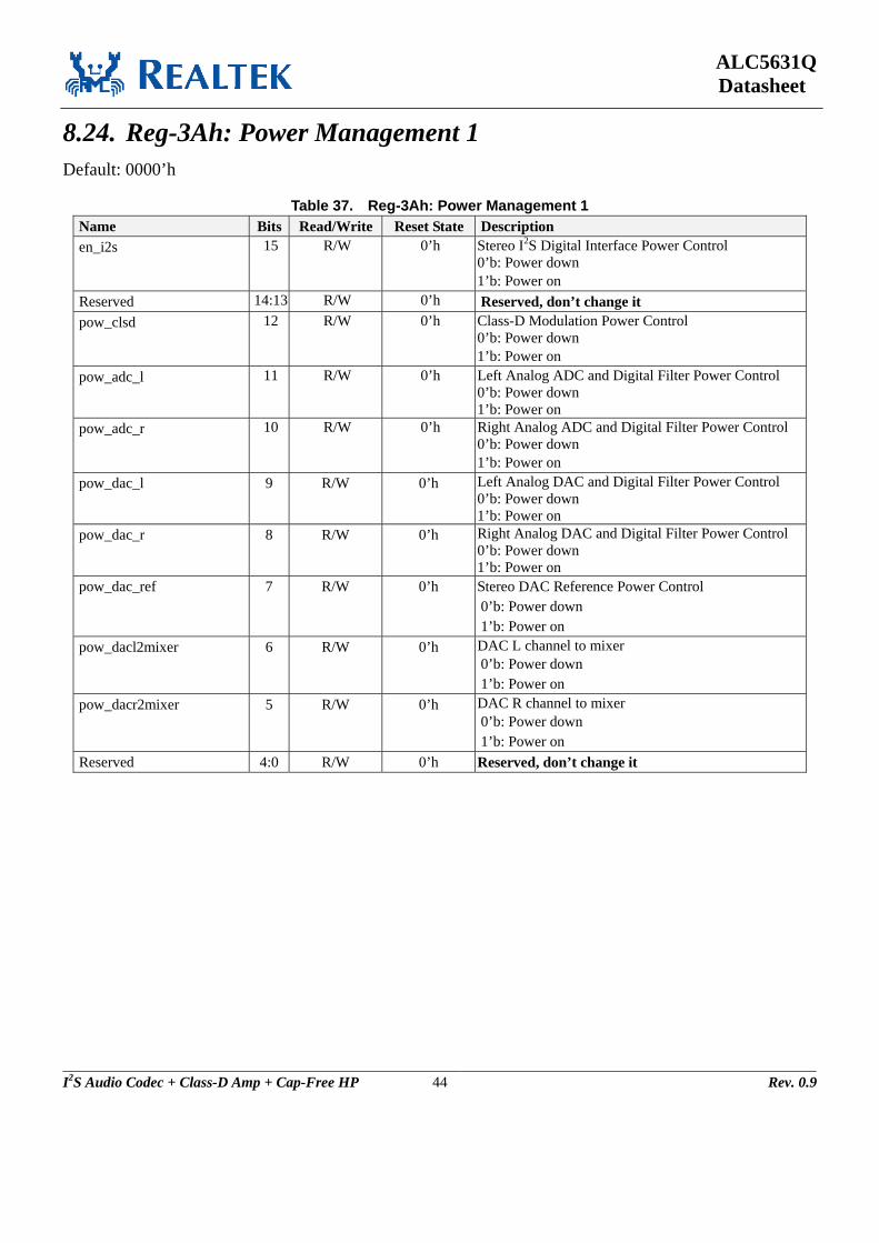
ALC5631Q Datasheet
I2S Audio Codec + Class-D Amp + Cap-Free HP 44 Rev. 0.9
8.24. Reg-3Ah: Power Management 1 Default: 0000’h
Table 37. Reg-3Ah: Power Management 1 Name Bits Read/Write Reset State Description en_i2s 15 R/W 0’h Stereo I2S Digital Interface Power Control
0’b: Power down 1’b: Power on
Reserved 14:13 R/W 0’h Reserved, don’t change it pow_clsd 12 R/W 0’h Class-D Modulation Power Control
0’b: Power down 1’b: Power on
pow_adc_l 11 R/W 0’h Left Analog ADC and Digital Filter Power Control 0’b: Power down 1’b: Power on
pow_adc_r 10 R/W 0’h Right Analog ADC and Digital Filter Power Control 0’b: Power down 1’b: Power on
pow_dac_l 9 R/W 0’h Left Analog DAC and Digital Filter Power Control 0’b: Power down 1’b: Power on
pow_dac_r 8 R/W 0’h Right Analog DAC and Digital Filter Power Control 0’b: Power down 1’b: Power on
pow_dac_ref 7 R/W 0’h Stereo DAC Reference Power Control 0’b: Power down 1’b: Power on
pow_dacl2mixer 6 R/W 0’h DAC L channel to mixer 0’b: Power down 1’b: Power on
pow_dacr2mixer 5 R/W 0’h DAC R channel to mixer 0’b: Power down 1’b: Power on
Reserved 4:0 R/W 0’h Reserved, don’t change it

ALC5631Q Datasheet
I2S Audio Codec + Class-D Amp + Cap-Free HP 45 Rev. 0.9
8.25. Reg-3Bh: Power Management 2 Default: 0000’h
Table 38. Reg-3Bh: Power Management 2 Name Bits Read/Write Reset State Description pow_outmixl 15 R/W 0’h Left Output Mixer (OUTMIXL) Power Control
0’b: Power down 1’b: Power on
pow_outmixr 14 R/W 0’h Right Output Mixer (OUTMIXR) Power Control 0’b: Power down 1’b: Power on
pow_spkmixl 13 R/W 0’h Left Speaker Mixer (SPKMIXL) Power Control 0’b: Power down 1’b: Power on
pow_spkmixr 12 R/W 0’h Right Speaker Mixer (SPKMIXR) Power Control 0’b: Power down 1’b: Power on
pow_recmixl 11 R/W 0’h Left REC Mixer (RECMIXL) Power Control 0’b: Power down 1’b: Power on
pow_recmixr 10 R/W 0’h Right REC Mixer (RECMIXR) Power Control 0’b: Power down 1’b: Power on
Reserved 9:6 - 0’h Reserved pow_mic1 5 R/W 0’h MIC1 Boost Gain Power Control
0’b: Power down 1’b: Power on
pow_mic2 4 R/W 0’h MIC2 Boost Gain Power Control 0’b: Power down 1’b: Power on
pow_micbias1 3 R/W 0’h MIC1 Bias Voltage Power Control 0’b: Power down 1’b: Power on
pow_micbias2 2 R/W 0’h MIC2 Bias Voltage Power Control 0’b: Power down 1’b: Power on
pllen_PLL 1 R/W 0’h PLL Power Control 0’b: Power down 1’b: Power on
Reserved 0 R/W 0’h Reserved, don’t change it

ALC5631Q Datasheet
I2S Audio Codec + Class-D Amp + Cap-Free HP 46 Rev. 0.9
8.26. Reg-3Ch: Power Management 3 Default: 0000’h
Table 39. Reg-3Ch: Power Management 3 Name Bits Read/Write Reset State Description pow_vref 15 R/W 0’h Vref Voltage Power Control
0’b: Power down 1’b: Power on
en_fastb 14 R/W 0’h Fast Vref Control 0’b: Enable 1’b: Disable (For beter analog performance)
pow_main_bias 13 R/W 0’h Analog Block Bias Control 0’b: Power down 1’b: Power on
Reserved 12 - 0’h Reserved pow_axo1 11 R/W 0’h AXO1 Mixer Power Control
0’b: Power down 1’b: Power on
pow_axo2 10 R/W 0’h AXO2 Mixer Power Control 0’b: Power down 1’b: Power on
pow_monomix 9 R/W 0’h MONO Mixer (MONOMIX) Power Control 0’b: Power down 1’b: Power on
en_out_mono 8 R/W 0’h MONOOUT Output Depop Mode Control 0’b: Enable depop mode 1’b: Disable depop mode
en_mono_amp 7 R/W 0’h MONOOUT Output Amplifier Driving Control 0’b: Disable amplifier driving (Without driving capability) 1’b: Enable amplifier driving (With driving capability)
reserved 6:5 - 0’h Reserved pow_cp_hp 4 R/W 0’h Charge Pump Power Control
0’b: Power down 1’b: Power on This register will be no used when pow_capless =1’b
pow_l_hp 3 R/W 0’h Headphone Amplifier Left Channel Power Control 0’b: Power down 1’b: Power on This register will be no used when pow_capless =1’b
pow_r_hp 2 R/W 0’h Headphone Amplifier Right Channel Power Control 0’b: Power down 1’b: Power on This register will be no used when pow_capless =1’b
en_out_hp 1 R/W 0’h Headphone Output Depop Mode Control 0’b: Depop mode 1’b: Normal mode This register will be no used when pow_capless =1’b

ALC5631Q Datasheet
I2S Audio Codec + Class-D Amp + Cap-Free HP 47 Rev. 0.9
Name Bits Read/Write Reset State Description Reserved 0 R/W 0’h Reserved, don’t change it
8.27. Reg-3Eh: Power Management 4 Default: 0000’h
Table 40. Reg-3Eh: Power Management 4 Name Bits Read/Write Reset State Description pow_spo_vol_l 15 R/W 0’h Left Speaker Volume (SPKLVOL) Power Control
0’b: Power down
1’b: Power on
pow_spo_vol_r 14 R/W 0’h Right Speaker Volume (SPKRVOR) Power Control 0’b: Power down
1’b: Power on
pow_o_vol_l 13 R/W 0’h Left Output Volume (OUTVOLL) Power Control 0’b: Power down
1’b: Power on
pow_o_vol_r 12 R/W 0’h Right Output Volume (OUTVOLR) Power Control 0’b: Power down
1’b: Power on
pow_hpo_vol_l 11 R/W 0’h Left Headphone Output Volume (HPOVOLL) Power Control 0’b: Power down
1’b: Power on
pow_hpo_vol_r 10 R/W 0’h Right Headphone Output Volume (HPOVOLR) Power Control 0’b: Power down
1’b: Power on
pow_axi_vol_l 9 R/W 0’h AXIL Input Volume Power Control 0’b: Power down
1’b: Power on
pow_axi_vol_r 8 R/W 0’h AXIR Input Volume Power Control 0’b: Power down 1’b: Power on
pow_rx_vol_p 7 R/W 0’h MONOIN_P Input Volume Power Control 0’b: Power down 1’b: Power on
pow_rx_vol_n 6 R/W 0’h MONOIN_ N Input Volume Power Control 0’b: Power down 1’b: Power on
Reserved 5:0 - 0’h Reserved

ALC5631Q Datasheet
I2S Audio Codec + Class-D Amp + Cap-Free HP 48 Rev. 0.9
8.28. Reg-40h: General Purpose Control Register Default: 0E00’h
Table 41. Reg-40h: General Purpose Control Register Name Bits Read/
Write Reset State
Description
en_spk_auto_ratio 15 R/W 0’h Speaker Amplifier Auto Ratio Gain Control 0’b: Disable (Manual Setting) 1’b: Enable (Auto Setting)
spk_gain 14:12 R/W 0’h Speaker Amplifier AC Ratio Gain Control 000’b: 1.00 × AVDD ( 0dB ) 001’b: 1.09 × AVDD ( 0.80dB ) 010’b: 1.27 × AVDD ( 2.10dB ) 011’b: 1.44 × AVDD ( 3.16dB ) 100’b: 1.56 × AVDD ( 3.86dB ) 101’b: 1.68 × AVDD ( 4.50dB ) 110’b: 1.99 × AVDD ( 5.99dB ) 111’b: 2.34 × AVDD ( 7.40dB ) Note: When en_spk_auto_ratio=0’b, this register can set AC gain ratio of SPK Amplifier. This Register is not work when en_spk_auto_ratio=1’b
en_dac_hpf 11 R/W 1’h Stereo DAC High-Pass-Filter (HPF) Control 0’b: Bypass HPF 1’b: With HPF
en_adc_hpf 10 R/W 1’h Stereo ADC High-Pass-Filter (HPF) Control 0’b: Bypass HPF 1’b: With HPF
Reserved 9:6 - 1’h Reserved, don’t change it sel_adhpf_fs_type 5:4 R/W 0’h Select ADC Wind Filter Clock Type
00’b: Type1 01’b: Type2 10’b: Type3 11’b: Reserved
en_adc_wf 3 R/W 0’h ADC Wind Filter Control 0’b: Disable 1’b: Enable
sel_adc_wf 2:0 R/W 0’h Select ADC Wind Filter Corner Frequency
Sampling Rate (sel_adhpf_fs_type) = 48kHz sel_adc_wf 00’b 01’b 10’b
000 130 Hz 260 Hz 440 Hz 001 170 Hz 330 Hz 556 Hz 010 171 Hz 330 Hz 556 Hz 011 254 Hz 448 Hz 770 Hz 100 330 Hz 640 Hz 1124 Hz 101 420 Hz 730 Hz 1200 Hz 110 509 Hz 770 Hz 2000 Hz 111 620 Hz 1260 Hz 2155 Hz
The setting of REG-40h_b5:4 is need to the same as I2S sample rate. Or will have frequency difference for corner frequency of wind filter.
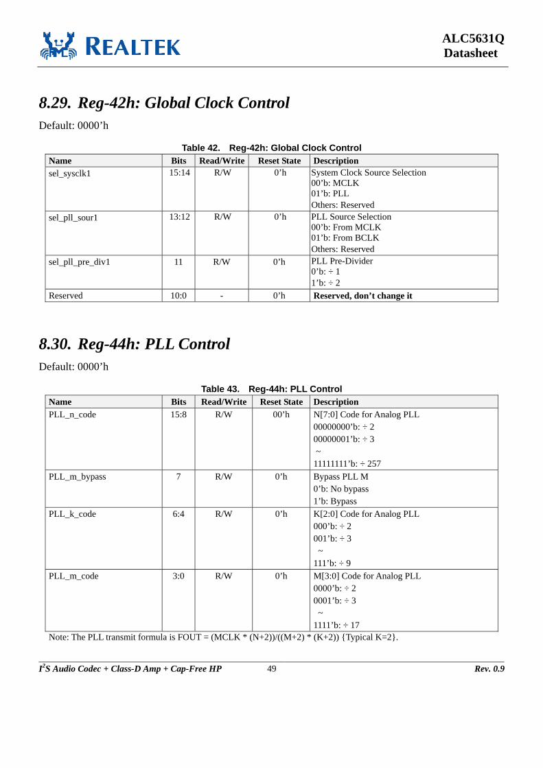
ALC5631Q Datasheet
I2S Audio Codec + Class-D Amp + Cap-Free HP 49 Rev. 0.9
8.29. Reg-42h: Global Clock Control Default: 0000’h
Table 42. Reg-42h: Global Clock Control Name Bits Read/Write Reset State Description sel_sysclk1 15:14 R/W 0’h System Clock Source Selection
00’b: MCLK 01’b: PLL Others: Reserved
sel_pll_sour1 13:12 R/W 0’h PLL Source Selection 00’b: From MCLK 01’b: From BCLK Others: Reserved
sel_pll_pre_div1 11 R/W 0’h PLL Pre-Divider 0’b: ÷ 1 1’b: ÷ 2
Reserved 10:0 - 0’h Reserved, don’t change it
8.30. Reg-44h: PLL Control Default: 0000’h
Table 43. Reg-44h: PLL Control Name Bits Read/Write Reset State Description PLL_n_code 15:8 R/W 00’h N[7:0] Code for Analog PLL
00000000’b: ÷ 2 00000001’b: ÷ 3 ~ 11111111’b: ÷ 257
PLL_m_bypass 7 R/W 0’h Bypass PLL M 0’b: No bypass 1’b: Bypass
PLL_k_code 6:4 R/W 0’h K[2:0] Code for Analog PLL 000’b: ÷ 2 001’b: ÷ 3 ~ 111’b: ÷ 9
PLL_m_code 3:0 R/W 0’h M[3:0] Code for Analog PLL 0000’b: ÷ 2 0001’b: ÷ 3 ~ 1111’b: ÷ 17
Note: The PLL transmit formula is FOUT = (MCLK * (N+2))/((M+2) * (K+2)) {Typical K=2}.

ALC5631Q Datasheet
I2S Audio Codec + Class-D Amp + Cap-Free HP 50 Rev. 0.9
8.30.1. PLL Clock Setting Table for 48K: (Unit: MHz) Table 44. PLL Clock Setting Table for 48K: (Unit: MHz)
MCLK N M FVCO K FOUT 13 66 7 98.222 2 24.555
3.6864 78 1 98.304 2 24.576 2.048 94 0 98.304 2 24.576 4.096 70 1 98.304 2 24.576
12 80 8 98.4 2 24.6 15.36 81 11 98.068 2 24.517
16 78 11 98.462 2 24.615 19.2 80 14 98.4 2 24.6
19.68 78 14 98.4 2 24.6
8.30.2. PLL Clock Setting Table for 44.1K: (Unit: MHz) Table 45. PLL Clock Setting Table for 44.1K: (Unit: MHz)
MCLK N M FVCO K FOUT 13 68 8 91 2 22.75
3.6864 72 1 90.931 2 22.733 2.048 86 0 90.112 2 22.528 4.096 64 1 90.112 2 22.528
12 66 7 90.667 2 22.667 15.36 63 9 90.764 2 22.691
16 66 10 90.667 2 22.667 19.2 64 12 90.514 2 22.629
19.68 67 13 90.528 2 22.632
8.31. Reg-48h: Internal Status and IRQ Control 1 Default: 0000’h
Table 46. Reg-48h: Internal Status and IRQ Control 1 Name Bits Read/Write Reset State Description en_irq_ovcd 15 R/W 0’h IRQ Output Source Decision for Over Current Status
0’b: Disable over current status to IRQ output 1’b: Enable over current status to IRQ output

ALC5631Q Datasheet
I2S Audio Codec + Class-D Amp + Cap-Free HP 51 Rev. 0.9
Name Bits Read/Write Reset State Description en_irq_ovtd 14 R/W 0’h IRQ Output Source Decision for Over Temperature
status 0’b: Disable over temperature status to IRQ output 1’b: Enable over temperature status to IRQ output
en_irq_jd 13 R/W 0’h IRQ Output Source Decision for Jack Detection Status 0’b: Disable jack detection status to IRQ output 1’b: Enable jack detection status to IRQ output
Reserved 12:2 - 0’h Reserved inv_ovtd 1 R/W 0’h Over Temperature Status Polarity
0’b: Normal 1’b: Output invert
inv_ovcd 0 R/W 0’h Speaker Amplifier Over Current Status Polarity 0’b: Normal 1’b: Output invert
8.32. Reg-4Ah: Internal Status and IRQ Control 2 Default: 0700’h
Table 47. Reg-4Ah: Internal Status and IRQ Control 2 Name Bits Read/Write Reset State Description en_adc_mono_source 15:14 R/W 0’h ADC MONO Mode Data source select:
00’b: Disable 01’b: From L-CH 10’b: From R-CH 11’b: Reserved
Reserved 13:4 - 38’h Reserved, don’t change it sta_jd_internal 3 R 0’h JD Status
0’b: Low 1’b: High
sta_gpio 2 R 0’h GPIO Pin Status 0’b: Low 1’b: High
ovt_status 1 R 0’h Over Temperature Sensor Status 0’b: Normal 1’b: Over temperature
sta_ovcd 0 R 0’h Speaker Amplifier Over Current Status 0’b: Normal 1’b: Over current
8.33. Reg-4Ch: GPIO Control Default: 0000’h
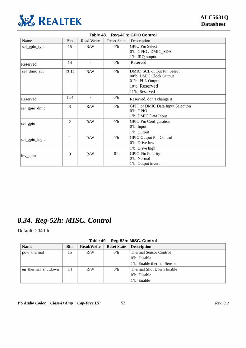
ALC5631Q Datasheet
I2S Audio Codec + Class-D Amp + Cap-Free HP 52 Rev. 0.9
Table 48. Reg-4Ch: GPIO Control Name Bits Read/Write Reset State Description sel_gpio_type 15 R/W 0’h GPIO Pin Select
0’b: GPIO / DMIC_SDA 1’b: IRQ output
Reserved 14 - 0’h Reserved
sel_dmic_scl 13:12 R/W 0’h DMIC_SCL output Pin Select 00’b: DMIC Clock Output 01’b: PLL Output 10’b: Reserved 11’b: Reserved
Reserved 11:4 - 0’h Reserved, don’t change it
sel_gpio_dmic 3 R/W 0’h GPIO or DMIC Data Input Selection 0’b: GPIO 1’b: DMIC Data Input
sel_gpio 2 R/W 0’h GPIO Pin Configuration 0’b: Input 1’b: Output
sel_gpio_logic 1 R/W 0’h GPIO Output Pin Control 0’b: Drive low 1’b: Drive high
inv_gpio 0 R/W 0’h GPIO Pin Polarity 0’b: Normal 1’b: Output invert
8.34. Reg-52h: MISC. Control Default: 2040’h
Table 49. Reg-52h: MISC. Control Name Bits Read/Write Reset State Description pow_thermal 15 R/W 0’h Thermal Sensor Control
0’b: Disable 1’b: Enable thermal Sensor
en_thermal_shutdown 14 R/W 0’h Thermal Shut Down Enable 0’b: Disable 1’b: Enable

ALC5631Q Datasheet
I2S Audio Codec + Class-D Amp + Cap-Free HP 53 Rev. 0.9
Name Bits Read/Write Reset State Description en_ovcd_hp 13 R/W 1’h Enable HP Amp Over Current Protection
0’b: Disable 1’b: Enable
Reserved 12 - 0’h Reserved sel_ovcd_th_hp 11:10 R/W 0’h HP Amp Over Current Protection Threshold
00’b: 100mA 01’b: 150mA 10’b: 200mA 11’b: 250mA
Reserved 9:8 - 0’h Reserved tmp_th_set 7:4 R/W 4’h Temperature Sensor Threshold Setting
0000’b: NA 0001’b: -40 oC 0010’b: -30 oC 0011’b: -10 oC 0100’b: +10 oC 0101’b: +30 oC 0110’b: +60 oC 0111’b: +70 oC 1000’b: +80 oC 1001’b: +90 oC 1010’b: +100 oC 1011’b: +110 oC 1100’b: +120 oC 1101’b: +130 oC 1110’b: +150 oC 1111’b: Reserved
Reserved 3:0 - 0’h Reserved
8.35. Reg-54h: De-POP Function Control 1 Default: 0000’h
Table 50. Reg-54h: De-POP Function Control 1 Name Bits Read/Write Reset State Description Pow_softgen_hp 15 R/W 0’h HP Soft Generator Control
0’b: Power down 1’b: Power on

ALC5631Q Datasheet
I2S Audio Codec + Class-D Amp + Cap-Free HP 54 Rev. 0.9
Name Bits Read/Write Reset State Description smttrig 14 R/W 0’h HP Softgen Trigger Control
0’b: Power down 1’b: Power on
Reserved 13 R/W 0’b Reserved, don’t change it En_dp_mono 12 R/W 0’b Enable De-pop Mode for MONO Amp
0’b: Disable 1’b: Enable
Reserved 11 R/W 0’b Reserved, don’t change it En_smt_mono 10 R/W 0’b Enable MONO Amp Mute/Un-Mute De-Pop
0’b: Disable 1’b: Enable
Pdn_mono 9 R/W 0’b Power Down MONO Amp Starts Up Signal 0’b: Disable 1’b: Enable
Reserved 8:7 R/W 0’h Reserved, don’t change it En_dp_hp 6 R/W 0’h Enable De-pop Mode for HPO
0’b: Disbale 1’b: Enable
Pdn_l_hp 5 R/W 0’h Power On HPO_L Start-Up Signal 0’b: Disable 1’b: Enable
Pdn_r_hp 4 R/W 0’h Power On HPO_R Start-Up Signal 0’b: Disable 1’b: Enable
reserved 3:2 - 0’h Reserved En_smt_l_hp 1 R/W 0’h Enable HPO_L Mute/Un-mute De-pop
0’b: Disable 1’b: Enable
En_smt_r_hp 0 R/W 0’h Enable HPO_R Mute/Un-mute De-pop 0’b: Disable 1’b: Enable
8.36. Reg-56h: De-POP Function Control Default: 0000’h
Table 51. Reg-56h: De-POP Function Control Name Bits Read/Write Reset State Description
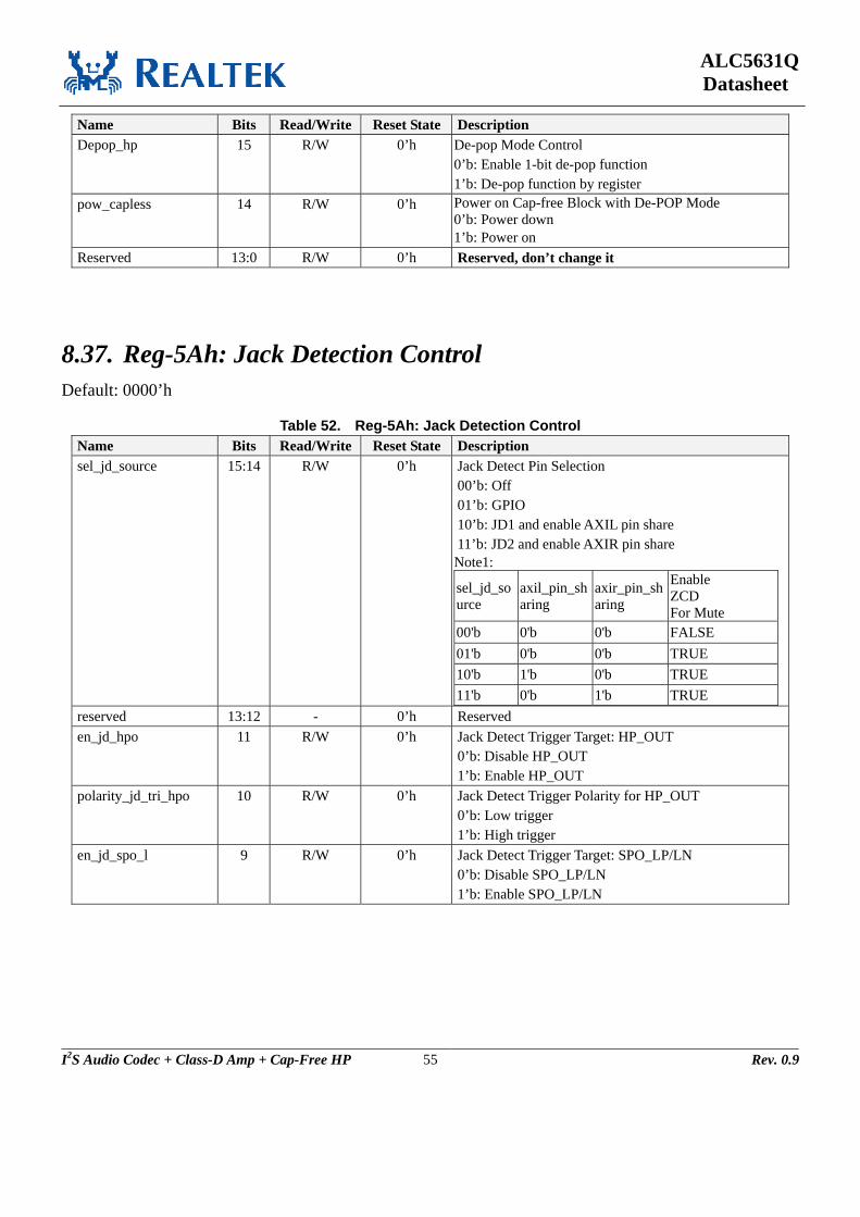
ALC5631Q Datasheet
I2S Audio Codec + Class-D Amp + Cap-Free HP 55 Rev. 0.9
Name Bits Read/Write Reset State Description Depop_hp 15 R/W 0’h De-pop Mode Control
0’b: Enable 1-bit de-pop function 1’b: De-pop function by register
pow_capless 14 R/W 0’h Power on Cap-free Block with De-POP Mode 0’b: Power down 1’b: Power on
Reserved 13:0 R/W 0’h Reserved, don’t change it
8.37. Reg-5Ah: Jack Detection Control Default: 0000’h
Table 52. Reg-5Ah: Jack Detection Control Name Bits Read/Write Reset State Description sel_jd_source 15:14 R/W 0’h Jack Detect Pin Selection
00’b: Off 01’b: GPIO 10’b: JD1 and enable AXIL pin share 11’b: JD2 and enable AXIR pin share Note1:
sel_jd_source
axil_pin_sharing
axir_pin_sharing
Enable ZCD For Mute
00'b 0'b 0'b FALSE 01'b 0'b 0'b TRUE 10'b 1'b 0'b TRUE 11'b 0'b 1'b TRUE
reserved 13:12 - 0’h Reserved en_jd_hpo 11 R/W 0’h Jack Detect Trigger Target: HP_OUT
0’b: Disable HP_OUT 1’b: Enable HP_OUT
polarity_jd_tri_hpo 10 R/W 0’h Jack Detect Trigger Polarity for HP_OUT 0’b: Low trigger 1’b: High trigger
en_jd_spo_l 9 R/W 0’h Jack Detect Trigger Target: SPO_LP/LN 0’b: Disable SPO_LP/LN 1’b: Enable SPO_LP/LN

ALC5631Q Datasheet
I2S Audio Codec + Class-D Amp + Cap-Free HP 56 Rev. 0.9
Name Bits Read/Write Reset State Description polarity_jd_tri_spo_l 8 R/W 0’h Jack Detect Trigger Polarity for SPO_LP/LN
0’b: Low trigger 1’b: High trigger
en_jd_spo_r 7 R/W 0’h Jack Detect Trigger Target: SPO_RP/RN 0’b: Disable SPO_RP/RN 1’b: Enable SPO_RP/RN
polarity_jd_tri_spo_r 6 R/W 0’h Jack Detect Trigger Polarity for SPO_RP/RN 0’b: Low trigger 1’b: High trigger
en_jd_mono 5 R/W 0’h Jack Detect Trigger Target: MONOOUT 0’b: Disable MONOOUT 1’b: Enable MONOOUT
polarity_jd_tri_mono 4 R/W 0’h Jack Detect Trigger Polarity for MONOOUT 0’b: Low trigger 1’b: High trigger
en_jd_axo1 3 R/W 0’h Jack Detect Trigger Target: AXO1 0’b: Disable AXO1 1’b: Enable AXO1
polarity_jd_tri_axo1 2 R/W 0’h Jack Detect Trigger Polarity AXO1 0’b: Low trigger 1’b: High trigger
en_jd_axo2 1 R/W 0’h Jack Detect Trigger Target: AXO2 0’b: Disable AXO2 1’b: Enable AXO2
polarity_jd_tri_axo2 0 R/W 0’h Jack Detect Polarity trigger AXO2 0’b: Low trigger 1’b: High trigger

ALC5631Q Datasheet
I2S Audio Codec + Class-D Amp + Cap-Free HP 57 Rev. 0.9
8.38. Reg-5Ch: Soft Volume Control Default: 07E9’h
Table 53. Reg-5Ch: Soft Volume Control Name Bits Read/Write Reset State Description en_softvol 15 R/W 0’h Digital Soft Volume Delay Control
0’b: Disable 1’b: Enable
en_spo_svol 14 R/W 0’h SPO L/R Soft Volume Delay Control 0’b: Disable 1’b: Enable
en_o_svol 13 R/W 0’h Output Soft Volume Delay Control 0’b: Disable 1’b: Enable
en_hpo_svol 12 R/W 0’h HPO Soft Volume Delay Control 0’b: Disable 1’b: Enable
en_rx_svol 11 R/W 0’h MONOIN Soft Volume Delay Control 0’b: Disable 1’b: Enable
pow_zcd 10 R/W 1’h Zero Crossing Control 0’b: Power down
1’b: Power on
en_axo1_zcd 9 R/W 1’h AXO1 Mute/Un-Mute Zero Crossing Control 0’b: Disable
1’b: Enable
en_axo2_zcd 8 R/W 1’h AXO2 Mute/Un-Mute Zero Crossing Control 0’b: Disable
1’b: Enable
en_spol_zcd 7 R/W 1’h SPO Left Channel Mute/Un-Mute Zero Crossing Control0’b: Disable
1’b: Enable
en_spor_zcd 6 R/W 1’h SPO Right Channel Mute/Un-Mute Zero Crossing Control 0’b: Disable
1’b: Enable
en_mono_zcd 5 R/W 1’h MONOOUT Mute/Un-Mute Zero Crossing Control 0’b: Disable
1’b: Enable
Reserved 4 - 0’h Reserved
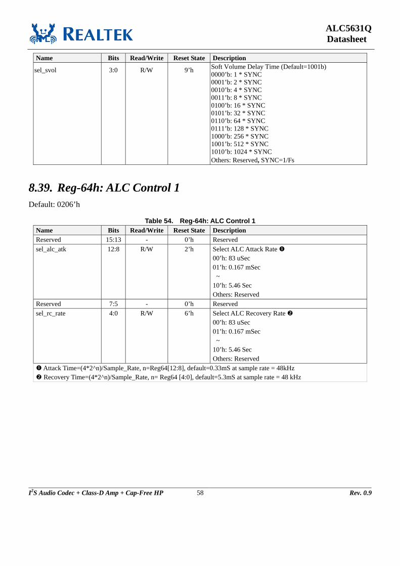
ALC5631Q Datasheet
I2S Audio Codec + Class-D Amp + Cap-Free HP 58 Rev. 0.9
Name Bits Read/Write Reset State Description
sel_svol 3:0 R/W 9’h Soft Volume Delay Time (Default=1001b) 0000’b: 1 * SYNC 0001’b: 2 * SYNC 0010’b: 4 * SYNC 0011’b: 8 * SYNC 0100’b: 16 * SYNC 0101’b: 32 * SYNC 0110’b: 64 * SYNC 0111’b: 128 * SYNC 1000’b: 256 * SYNC 1001’b: 512 * SYNC 1010’b: 1024 * SYNC Others: Reserved, SYNC=1/Fs
8.39. Reg-64h: ALC Control 1 Default: 0206’h
Table 54. Reg-64h: ALC Control 1 Name Bits Read/Write Reset State Description Reserved 15:13 - 0’h Reserved sel_alc_atk 12:8 R/W 2’h Select ALC Attack Rate
00’h: 83 uSec 01’h: 0.167 mSec ~ 10’h: 5.46 Sec Others: Reserved
Reserved 7:5 - 0’h Reserved sel_rc_rate 4:0 R/W 6’h Select ALC Recovery Rate
00’h: 83 uSec 01’h: 0.167 mSec ~ 10’h: 5.46 Sec Others: Reserved
Attack Time=(4*2^n)/Sample_Rate, n=Reg64[12:8], default=0.33mS at sample rate = 48kHz Recovery Time=(4*2^n)/Sample_Rate, n= Reg64 [4:0], default=5.3mS at sample rate = 48 kHz

ALC5631Q Datasheet
I2S Audio Codec + Class-D Amp + Cap-Free HP 59 Rev. 0.9
8.40. Reg-65h: ALC Control 2 Default: 0000’h
Table 55. Reg-65h: ALC Control 2 Name Bits Read/Write Reset State Description Reserved 15:4 - 0’h Reserved noise_gate_boost 3:0 R/W 0’h Noise Level Reduction Gain when Signal is Below Noise
Gate Level. 0000’b: 0dB 0001’b: 3dB 0010’b: 6dB ~ 1110’b: 42dB 1111’b: 45dB
When signal is below noise gate, can select gain to reduce noise level. The noise level is equal to - (original noise level + reduction gain)
8.41. Reg-66h: ALC Control 3 Default: 2000’h
Table 56. Reg-66h: ALC Control 3 Name Bits Read/Write Reset State Description sel_alc 15 R/W 0’h ALC Select
0’b: Enable ALC for DAC path 1’b: Enable ALC for ADC path
alc_en 14 R/W 0’h ALC Enable 1’b: ALC enable 0’b: ALC disable
update_alc_param 13 R/W 1’h Update ALC Parameter Write 1’b to update all ALC parameter then auto clear to zero
sel_alc_thmax 12:8 R/W 0’h ALC Limit Level 00’h: 0dBFS 01’h: -1.5dBFS 02’h: -3dBFS 03’h: -4.5dBFS ~ 1F’h: -46.5dBFS
en_alc_noise_gate 7 R/W 0’h Noise Gate Function Control 0’b: Disable 1’b: Enable
en_alc_noise_gate_hold 6 R/W 0’h Enable Noise Gate Hold Data Function 0’b: Disable 1’b: Enable
Reserved 5 - 0’h Reserved
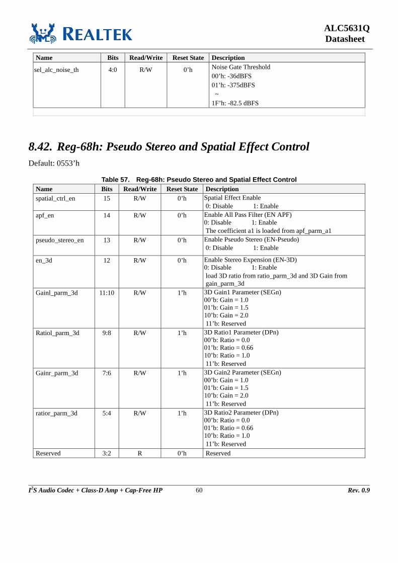
ALC5631Q Datasheet
I2S Audio Codec + Class-D Amp + Cap-Free HP 60 Rev. 0.9
Name Bits Read/Write Reset State Description
sel_alc_noise_th 4:0 R/W 0’h Noise Gate Threshold 00’h: -36dBFS 01’h: -375dBFS ~ 1F’h: -82.5 dBFS
8.42. Reg-68h: Pseudo Stereo and Spatial Effect Control Default: 0553’h
Table 57. Reg-68h: Pseudo Stereo and Spatial Effect Control Name Bits Read/Write Reset State Description spatial_ctrl_en 15 R/W 0’h Spatial Effect Enable
0: Disable 1: Enable apf_en 14 R/W 0’h Enable All Pass Filter (EN APF)
0: Disable 1: Enable The coefficient a1 is loaded from apf_parm_a1
pseudo_stereo_en 13 R/W 0’h Enable Pseudo Stereo (EN-Pseudo) 0: Disable 1: Enable
en_3d 12 R/W 0’h Enable Stereo Expension (EN-3D) 0: Disable 1: Enable load 3D ratio from ratio_parm_3d and 3D Gain from gain_parm_3d
Gainl_parm_3d 11:10 R/W 1’h 3D Gain1 Parameter (SEGn) 00’b: Gain = 1.0 01’b: Gain = 1.5 10’b: Gain = 2.0 11’b: Reserved
Ratiol_parm_3d 9:8 R/W 1’h 3D Ratio1 Parameter (DPn) 00’b: Ratio = 0.0 01’b: Ratio = 0.66 10’b: Ratio = 1.0 11’b: Reserved
Gainr_parm_3d 7:6 R/W 1’h 3D Gain2 Parameter (SEGn) 00’b: Gain = 1.0 01’b: Gain = 1.5 10’b: Gain = 2.0 11’b: Reserved
ratior_parm_3d 5:4 R/W 1’h 3D Ratio2 Parameter (DPn) 00’b: Ratio = 0.0 01’b: Ratio = 0.66 10’b: Ratio = 1.0 11’b: Reserved
Reserved 3:2 R 0’h Reserved
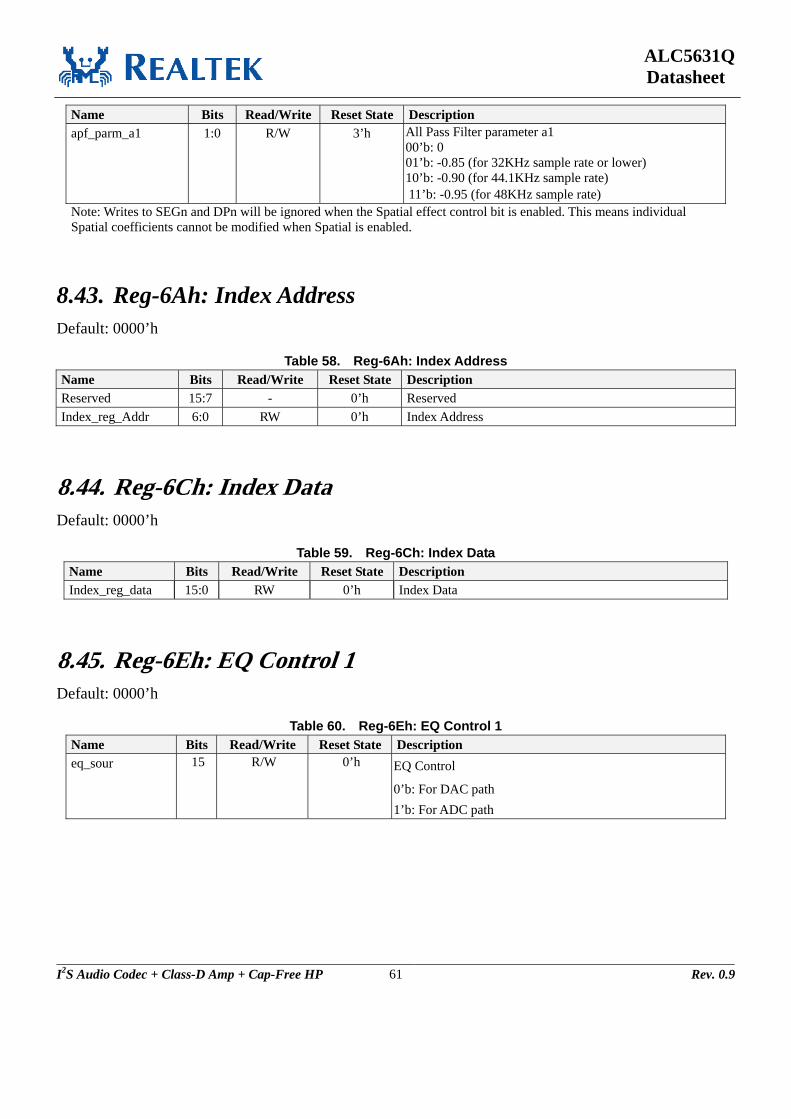
ALC5631Q Datasheet
I2S Audio Codec + Class-D Amp + Cap-Free HP 61 Rev. 0.9
Name Bits Read/Write Reset State Description apf_parm_a1 1:0 R/W 3’h All Pass Filter parameter a1
00’b: 0 01’b: -0.85 (for 32KHz sample rate or lower) 10’b: -0.90 (for 44.1KHz sample rate) 11’b: -0.95 (for 48KHz sample rate)
Note: Writes to SEGn and DPn will be ignored when the Spatial effect control bit is enabled. This means individual Spatial coefficients cannot be modified when Spatial is enabled.
8.43. Reg-6Ah: Index Address Default: 0000’h
Table 58. Reg-6Ah: Index Address Name Bits Read/Write Reset State Description Reserved 15:7 - 0’h Reserved Index_reg_Addr 6:0 RW 0’h Index Address
8.44. Reg-6Ch: Index Data Default: 0000’h
Table 59. Reg-6Ch: Index Data Name Bits Read/Write Reset State Description Index_reg_data 15:0 RW 0’h Index Data
8.45. Reg-6Eh: EQ Control 1 Default: 0000’h
Table 60. Reg-6Eh: EQ Control 1 Name Bits Read/Write Reset State Description eq_sour 15 R/W 0’h EQ Control
0’b: For DAC path 1’b: For ADC path
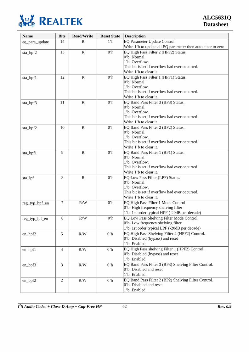
ALC5631Q Datasheet
I2S Audio Codec + Class-D Amp + Cap-Free HP 62 Rev. 0.9
Name Bits Read/Write Reset State Description eq_para_update 14 R 1’h EQ Parameter Update Control
Write 1’b to update all EQ parameter then auto clear to zero sta_hpf2 13 R 0’h EQ High Pass Filter 2 (HPF2) Status.
0’b: Normal 1’b: Overflow. This bit is set if overflow had ever occurred. Write 1’b to clear it.
sta_hpf1 12 R 0’h EQ High Pass Filter 1 (HPF1) Status. 0’b: Normal 1’b: Overflow. This bit is set if overflow had ever occurred. Write 1’b to clear it.
sta_bpf3 11 R 0’h EQ Band Pass Filter 3 (BP3) Status. 0’b: Normal 1’b: Overflow. This bit is set if overflow had ever occurred. Write 1’b to clear it.
sta_bpf2 10 R 0’h EQ Band Pass Filter 2 (BP2) Status. 0’b: Normal 1’b: Overflow. This bit is set if overflow had ever occurred. Write 1’b to clear it.
sta_bpf1 9 R 0’h EQ Band Pass Filter 1 (BP1) Status. 0’b: Normal 1’b: Overflow. This bit is set if overflow had ever occurred. Write 1’b to clear it.
sta_lpf 8 R 0’h EQ Low Pass Filter (LPF) Status. 0’b: Normal 1’b: Overflow. This bit is set if overflow had ever occurred. Write 1’b to clear it.
reg_typ_hpf_en 7 R/W 0’h EQ High Pass Filter 1 Mode Control 0’b: High frequency shelving filter 1’b: 1st order typical HPF (-20dB per decade)
reg_typ_lpf_en 6 R/W 0’h EQ Low Pass Shelving Filter Mode Control 0’b: Low frequency shelving filter 1’b: 1st order typical LPF (-20dB per decade)
en_hpf2 5 R/W 0’h EQ High Pass Shelving Filter 2 (HPF2) Control. 0’b: Disabled (bypass) and reset 1’b: Enabled
en_hpf1 4 R/W 0’h EQ High Pass shelving Filter 1 (HPF2) Control. 0’b: Disabled (bypass) and reset 1’b: Enabled
en_bpf3 3 R/W 0’h EQ Band Pass Filter 3 (BP3) Shelving Filter Control. 0’b: Disabled and reset 1’b: Enabled.
en_bpf2 2 R/W 0’h EQ Band Pass Filter 2 (BP2) Shelving Filter Control. 0’b: Disabled and reset 1’b: Enabled.
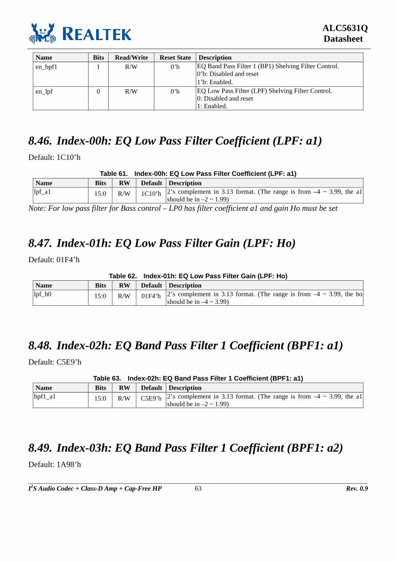
ALC5631Q Datasheet
I2S Audio Codec + Class-D Amp + Cap-Free HP 63 Rev. 0.9
Name Bits Read/Write Reset State Description en_bpf1 1 R/W 0’h EQ Band Pass Filter 1 (BP1) Shelving Filter Control.
0’b: Disabled and reset 1’b: Enabled.
en_lpf 0 R/W 0’h EQ Low Pass Filter (LPF) Shelving Filter Control. 0: Disabled and reset 1: Enabled.
8.46. Index-00h: EQ Low Pass Filter Coefficient (LPF: a1) Default: 1C10’h
Table 61. Index-00h: EQ Low Pass Filter Coefficient (LPF: a1) Name Bits RW Default Description lpf_a1 15:0 R/W 1C10’h 2’s complement in 3.13 format. (The range is from –4 ~ 3.99, the a1
should be in –2 ~ 1.99) Note: For low pass filter for Bass control – LP0 has filter coefficient a1 and gain Ho must be set
8.47. Index-01h: EQ Low Pass Filter Gain (LPF: Ho) Default: 01F4’h
Table 62. Index-01h: EQ Low Pass Filter Gain (LPF: Ho) Name Bits RW Default Description lpf_h0 15:0 R/W 01F4’h 2’s complement in 3.13 format. (The range is from –4 ~ 3.99, the ho
should be in –4 ~ 3.99)
8.48. Index-02h: EQ Band Pass Filter 1 Coefficient (BPF1: a1) Default: C5E9’h
Table 63. Index-02h: EQ Band Pass Filter 1 Coefficient (BPF1: a1) Name Bits RW Default Description bpf1_a1 15:0 R/W C5E9’h 2’s complement in 3.13 format. (The range is from –4 ~ 3.99, the a1
should be in –2 ~ 1.99)
8.49. Index-03h: EQ Band Pass Filter 1 Coefficient (BPF1: a2) Default: 1A98’h

ALC5631Q Datasheet
I2S Audio Codec + Class-D Amp + Cap-Free HP 64 Rev. 0.9
Table 64. Index-03h: EQ Band Pass Filter 1 Coefficient (BPF1: a2) Name Bits RW Default Description bpf1_a2 15:0 R/W 1A98’h 2’s complement in 3.13 format. (The range is from –4 ~ 3.99, the a2
should be in –2 ~ 1.99)
8.50. Index-04h: EQ Band Pass Filter 1 Gain (BPF1: Ho) Default: 1D2C’h
Table 65. Index-04h: EQ Band Pass Filter 1 Gain (BPF1: Ho) Name Bits RW Default Description bpf1_h0 15:0 R/W 1D2C’h 2’s complement in 3.13 format. (The range is from –4 ~ 3.99, the ho
should be in –4 ~ 3.99)
8.51. Index-05h: EQ Band Pass Filter 2 Coefficient (BPF2: a1) Default: C882’h
Table 66. Index-05h: EQ Band Pass Filter 2 Coefficient (BPF2: a1) Name Bits RW Default Description bpf2_a1 15:0 R/W C882’h 2’s complement in 3.13 format. (The range is from –4 ~ 3.99, the a1
should be in –2 ~ 1.99)
8.52. Index-06h: EQ Band Pass Filter 2 Coefficient (BPF2: a2) Default: 1C10’h
Table 67. Index-06h: EQ Band Pass Filter 2 Coefficient (BPF2: a2) Name Bits RW Default Description bpf2_a2 15:0 R/W 1C10’h 2’s complement in 3.13 format. (The range is from –4 ~ 3.99, the a2
should be in –2 ~ 1.99)
8.53. Index-07h: EQ Band Pass Filter 2 Gain (BPF2: Ho) Default: 01F4’h
Table 68. Index-07h: EQ Band Pass Filter 2 Gain (BPF2: Ho) Name Bits RW Default Description bpf2_h0 15:0 R/W 01F4’h 2’s complement in 3.13 format. (The range is from –4 ~ 3.99, the ho
should be in –4 ~ 3.99)
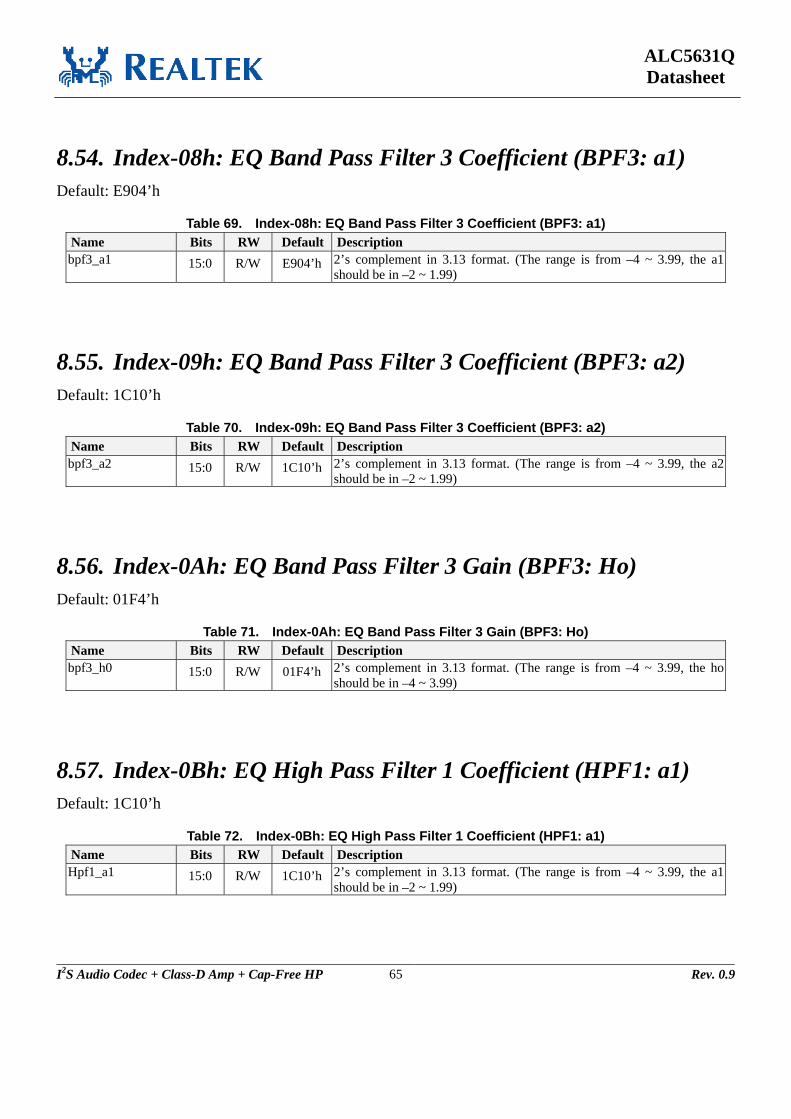
ALC5631Q Datasheet
I2S Audio Codec + Class-D Amp + Cap-Free HP 65 Rev. 0.9
8.54. Index-08h: EQ Band Pass Filter 3 Coefficient (BPF3: a1) Default: E904’h
Table 69. Index-08h: EQ Band Pass Filter 3 Coefficient (BPF3: a1) Name Bits RW Default Description bpf3_a1 15:0 R/W E904’h 2’s complement in 3.13 format. (The range is from –4 ~ 3.99, the a1
should be in –2 ~ 1.99)
8.55. Index-09h: EQ Band Pass Filter 3 Coefficient (BPF3: a2) Default: 1C10’h
Table 70. Index-09h: EQ Band Pass Filter 3 Coefficient (BPF3: a2) Name Bits RW Default Description bpf3_a2 15:0 R/W 1C10’h 2’s complement in 3.13 format. (The range is from –4 ~ 3.99, the a2
should be in –2 ~ 1.99)
8.56. Index-0Ah: EQ Band Pass Filter 3 Gain (BPF3: Ho) Default: 01F4’h
Table 71. Index-0Ah: EQ Band Pass Filter 3 Gain (BPF3: Ho) Name Bits RW Default Description bpf3_h0 15:0 R/W 01F4’h 2’s complement in 3.13 format. (The range is from –4 ~ 3.99, the ho
should be in –4 ~ 3.99)
8.57. Index-0Bh: EQ High Pass Filter 1 Coefficient (HPF1: a1) Default: 1C10’h
Table 72. Index-0Bh: EQ High Pass Filter 1 Coefficient (HPF1: a1) Name Bits RW Default Description Hpf1_a1 15:0 R/W 1C10’h 2’s complement in 3.13 format. (The range is from –4 ~ 3.99, the a1
should be in –2 ~ 1.99)

ALC5631Q Datasheet
I2S Audio Codec + Class-D Amp + Cap-Free HP 66 Rev. 0.9
8.58. Index-0Ch: EQ High Pass Filter 1 Gain (HPF1: Ho) Default: 01F4’h
Table 73. Index-0Ch: EQ High Pass Filter 1 Gain (HPF1: Ho) Name Bits RW Default Description Hpf1_h0 15:0 R/W 01F4’h 2’s complement in 3.13 format. (The range is from –4 ~ 3.99, the ho
should be in –4 ~ 3.99)
8.59. Index-0Dh: EQ High Pass Filter 2 Coefficient (HPF2: a1) Default: C01E’h
Table 74. Index-0Dh: EQ High Pass Filter 2 Coefficient (HPF1: a1) Name Bits RW Default Description Hpf2_a1 15:0 R/W C01E’h 2’s complement in 3.13 format. (The range is from –4 ~ 3.99, the a1
should be in –2 ~ 1.99)
8.60. Index-0Eh: EQ High Pass Filter 2 Coefficient (HPF2: a2) Default: 1FE2’h
Table 75. Index-0Eh: EQ High Pass Filter 2 Coefficient (HPF1: a2) Name Bits RW Default Description Hpf2_a2 15:0 R/W 1FE2’h 2’s complement in 3.13 format. (The range is from –4 ~ 3.99, the a1
should be in –2 ~ 1.99)
8.61. Index-0Fh: EQ High Pass Filter 2 Gain (HPF2: Ho) Default: 1FF1’h
Table 76. Index-0Fh: EQ High Pass Filter 2 Gain (HPF2: Ho) Name Bits RW Default Description Hpf2_h0 15:0 R/W 1FF1’h 2’s complement in 3.13 format. (The range is from –4 ~ 3.99, the ho
should be in –4 ~ 3.99)
8.62. Index-11h: EQ Input Volume Control Default: 8000’h

ALC5631Q Datasheet
I2S Audio Codec + Class-D Amp + Cap-Free HP 67 Rev. 0.9
Table 77. Index-11h: EQ Input Volume Control Name Bits RW Default Description eq_sel_hidden 15 R/W 1’h EQ Block Control
0’b: Disable (Bypass EQ) 1’b: Enable
reserved 14:3 R 0’h Reserved
reg_eq_pre_vol 2:0 R/W 0’h Volume Unsigned Ratio EQIn-VOL-LR 000’b: 0dB 001’b: -3dB 010’b: -6dB 011’b: -9dB 100’b: -12dB 101’b: -15dB 110’b: -18dB 111’b: -21dB
Note: Individual EQ coefficients cannot be modified when EQ is enabled.
8.63. Index-12h: EQ Output Volume Control Default: 0003’h
Table 78. Index-12h: EQ Output Volume Control Name Bits RW Default Description reserved 15:4 R 0’h Reserved
reg_eq_post_vol 3:0 R/W 3’h Volume Unsigned Ratio EQOut-VOL-LR 0000’b: -4.5dB 0001’b: -3dB 0010’b: -1.5dB 0011’b: 0dB 0100’b: 1.5dB 0101’b: 3dB 0110’b: 4.5dB 0111’b: 6dB 1000’b: 7.5dB 1001’b: 9dB 1010’b: 10.5dB 1011’b: 12dB 1100’b: 13.5dB 1101’b: 15dB 1110’b: 16.5dB 1111’b: 18dB
8.64. Index-20h: ALC DAC Digital Volume Default: 0000’h
Table 79. Index-20XXh: ALC DAC Digital Volume Name Bits RW Default Description sta_vol_dac_l 15:8 R 0’h DAC left channel digital volume in 0.375 dB step
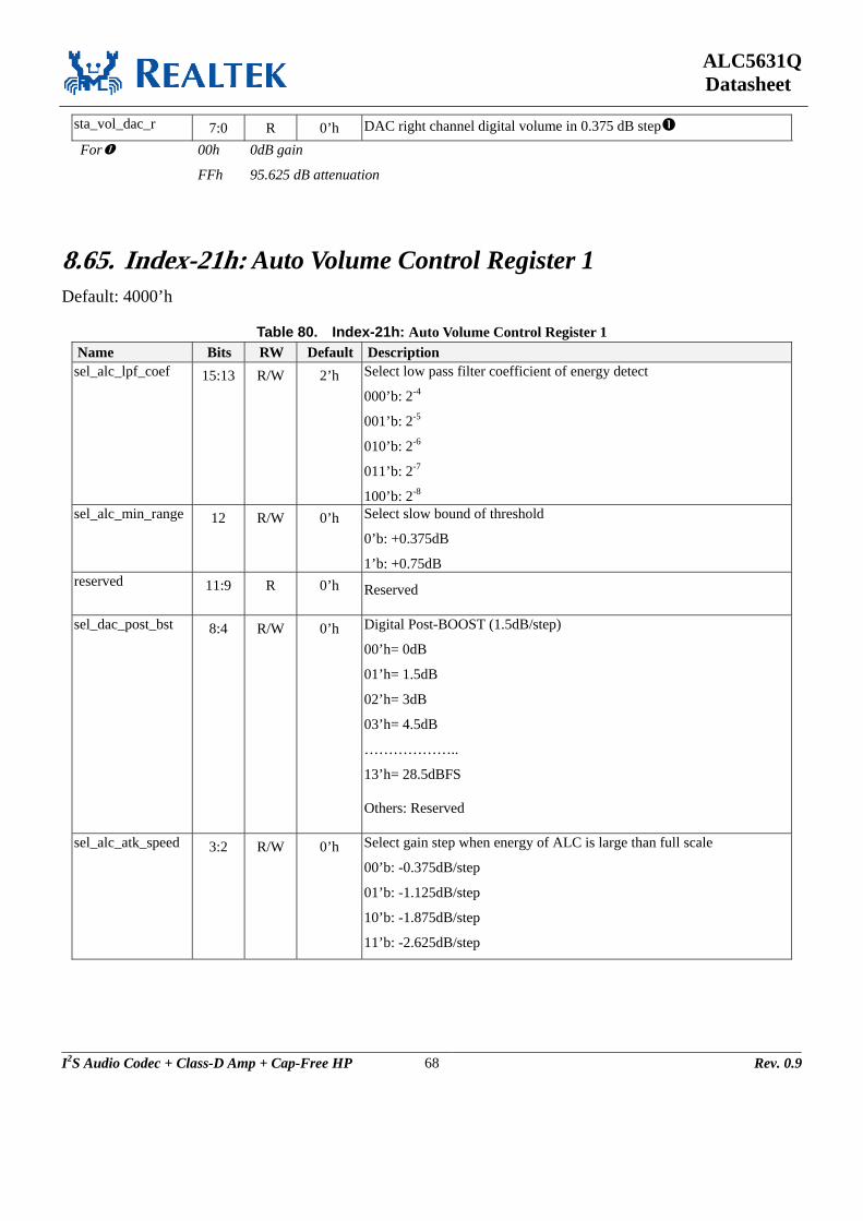
ALC5631Q Datasheet
I2S Audio Codec + Class-D Amp + Cap-Free HP 68 Rev. 0.9
sta_vol_dac_r 7:0 R 0’h DAC right channel digital volume in 0.375 dB step For 00h
FFh
0dB gain
95.625 dB attenuation
8.65. Index-21h: Auto Volume Control Register 1 Default: 4000’h
Table 80. Index-21h: Auto Volume Control Register 1 Name Bits RW Default Description sel_alc_lpf_coef 15:13 R/W 2’h Select low pass filter coefficient of energy detect
000’b: 2-4
001’b: 2-5
010’b: 2-6
011’b: 2-7
100’b: 2-8 sel_alc_min_range 12 R/W 0’h Select slow bound of threshold
0’b: +0.375dB
1’b: +0.75dB reserved 11:9 R 0’h Reserved
sel_dac_post_bst 8:4 R/W 0’h Digital Post-BOOST (1.5dB/step)
00’h= 0dB
01’h= 1.5dB
02’h= 3dB
03’h= 4.5dB
………………..
13’h= 28.5dBFS
Others: Reserved
sel_alc_atk_speed 3:2 R/W 0’h Select gain step when energy of ALC is large than full scale
00’b: -0.375dB/step
01’b: -1.125dB/step
10’b: -1.875dB/step
11’b: -2.625dB/step

ALC5631Q Datasheet
I2S Audio Codec + Class-D Amp + Cap-Free HP 69 Rev. 0.9
sel_alc_full_th 1:0 R/W 0’h Full scale targe
00’b: 0dBFS
01’b: -1.5dBFS
10’b: -3dBFS
11’b: -4.5dBFS
8.66. Index-22h: Auto Volume Control Register 2 Default: A280’h
Table 81. Index-22h: Auto Volume Control Register 2 Name Bits RW Default Description en_rc_fast 15 R/W 1’h Enable Fast recovery
0’b: Disable
1’b: Enable ctl_alc_force_fast_rc
14 R/W 0’h ALC force fast recovery control
0’b: Disable Force fast recovery
1’b: Enable Force fast recovery immediately en_alc_force_fast_rc
13 R/W 1’h Enable ALC force fast recovery control
0’b: Disable fast recovery for special case
1’b: Enable fast recovery for normal use
sel_alc_fast_rate 12:8 R/W 2’h Select fast ALC recovery rate
00’h: 83 uSec
01’h: 0.167 mSec
………………..
10’h: 5.46 Sec
Others: Reserved
en_alc_zero_data 7 R/W 1’h Enable zero date detection
0’b: Disable
1’b: Enable
Reserved 6:3 R 0’h Reserved

ALC5631Q Datasheet
I2S Audio Codec + Class-D Amp + Cap-Free HP 70 Rev. 0.9
sel_alc_zero_th 2:0 R/W 0’h Zero Date Threshold (-1.5dB/step)
000’b: -84dBFS
001’b: -85.5dBFS
010’b: -87dBFS
011’b: -88.5dBFS
100’b: -90dBFS
101’b: -91.5dBFS
110’b: -93dBFS
111’b: -94.5dBFS
Fast recovery time=(4*2^n)/Sample_Rate, n=PR22[12:8], default=0.33mS HEX DEC Fast Attack Time
0 0 8.33333E-05
1 1 0.000166667
2 2 0.000333333
3 3 0.000666667
4 4 0.001333333
5 5 0.002666667
6 6 0.005333333
7 7 0.010666667
8 8 0.021333333
9 9 0.042666667
A 10 0.085333333
B 11 0.170666667
C 12 0.341333333
D 13 0.682666667
E 14 1.365333333
F 15 2.730666667
10 16 5.461333333
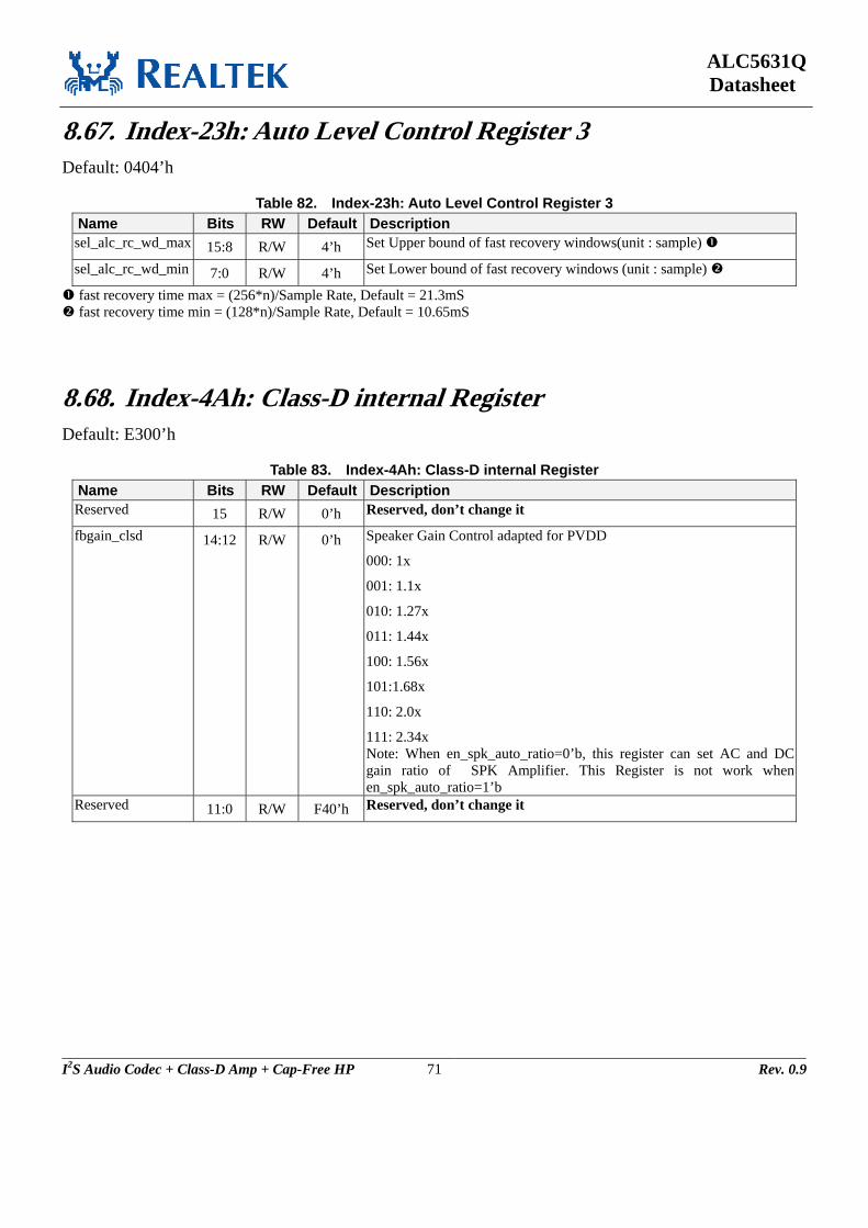
ALC5631Q Datasheet
I2S Audio Codec + Class-D Amp + Cap-Free HP 71 Rev. 0.9
8.67. Index-23h: Auto Level Control Register 3 Default: 0404’h
Table 82. Index-23h: Auto Level Control Register 3 Name Bits RW Default Description sel_alc_rc_wd_max 15:8 R/W 4’h Set Upper bound of fast recovery windows(unit : sample)
sel_alc_rc_wd_min 7:0 R/W 4’h Set Lower bound of fast recovery windows (unit : sample)
fast recovery time max = (256*n)/Sample Rate, Default = 21.3mS fast recovery time min = (128*n)/Sample Rate, Default = 10.65mS
8.68. Index-4Ah: Class-D internal Register Default: E300’h
Table 83. Index-4Ah: Class-D internal Register Name Bits RW Default Description Reserved 15 R/W 0’h Reserved, don’t change it
fbgain_clsd 14:12 R/W 0’h Speaker Gain Control adapted for PVDD
000: 1x
001: 1.1x
010: 1.27x
011: 1.44x
100: 1.56x
101:1.68x
110: 2.0x
111: 2.34x Note: When en_spk_auto_ratio=0’b, this register can set AC and DC gain ratio of SPK Amplifier. This Register is not work when en_spk_auto_ratio=1’b
Reserved 11:0 R/W F40’h Reserved, don’t change it

ALC5631Q Datasheet
I2S Audio Codec + Class-D Amp + Cap-Free HP 72 Rev. 0.9
8.69. Reg-7Ch: Vendor ID 1 Default: 10EC’h
Table 84. Reg-7Ch: Vendor ID 1 Name Bits Read/Write Reset State Description vender_id1 15:0 R 10EC’h Vendor ID=10EC
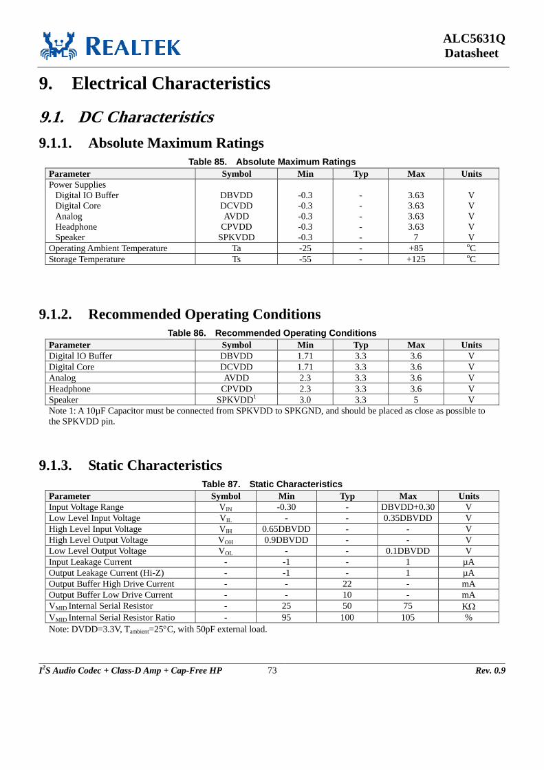
ALC5631Q Datasheet
I2S Audio Codec + Class-D Amp + Cap-Free HP 73 Rev. 0.9
9. Electrical Characteristics
9.1. DC Characteristics 9.1.1. Absolute Maximum Ratings
Table 85. Absolute Maximum Ratings Parameter Symbol Min Typ Max Units Power Supplies
Digital IO Buffer Digital Core Analog Headphone Speaker
DBVDD DCVDD AVDD
CPVDD SPKVDD
-0.3 -0.3 -0.3 -0.3 -0.3
- - - - -
3.63 3.63 3.63 3.63
7
V V V V V
Operating Ambient Temperature Ta -25 - +85 oC Storage Temperature Ts -55 - +125 oC
9.1.2. Recommended Operating Conditions Table 86. Recommended Operating Conditions
Parameter Symbol Min Typ Max Units Digital IO Buffer DBVDD 1.71 3.3 3.6 V Digital Core DCVDD 1.71 3.3 3.6 V Analog AVDD 2.3 3.3 3.6 V Headphone CPVDD 2.3 3.3 3.6 V Speaker SPKVDD1 3.0 3.3 5 V Note 1: A 10µF Capacitor must be connected from SPKVDD to SPKGND, and should be placed as close as possible to the SPKVDD pin.
9.1.3. Static Characteristics Table 87. Static Characteristics
Parameter Symbol Min Typ Max Units Input Voltage Range VIN -0.30 - DBVDD+0.30 V Low Level Input Voltage VIL - - 0.35DBVDD V High Level Input Voltage VIH 0.65DBVDD - - V High Level Output Voltage VOH 0.9DBVDD - - V Low Level Output Voltage VOL - - 0.1DBVDD V Input Leakage Current - -1 - 1 µA Output Leakage Current (Hi-Z) - -1 - 1 µA Output Buffer High Drive Current - - 22 - mA Output Buffer Low Drive Current - - 10 - mA VMID Internal Serial Resistor - 25 50 75 KΩ VMID Internal Serial Resistor Ratio - 95 100 105 % Note: DVDD=3.3V, Tambient=25°C, with 50pF external load.
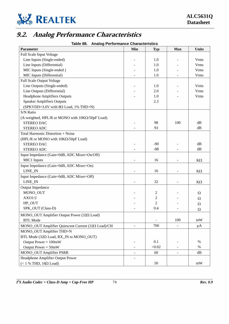
ALC5631Q Datasheet
I2S Audio Codec + Class-D Amp + Cap-Free HP 74 Rev. 0.9
9.2. Analog Performance Characteristics Table 88. Analog Performance Characteristics
Parameter Min Typ Max Units Full Scale Input Voltage
Line Inputs (Single-ended) Line Inputs (Differential) MIC Inputs (Single-ended ) MIC Inputs (Differential)
- - - -
1.0 1.0 1.0 1.0
- - - -
Vrms Vrms Vrms Vrms
Full Scale Output Voltage Line Outputs (Single-ended) Line Outputs (Differential) Headphone Amplifiers Outputs Speaker Amplifiers Outputs (SPKVDD=3.6V with 8Ω Load, 1% THD+N)
- - -
1.0 2.0 1.0 2.3
- - -
Vrms Vrms Vrms
S/N Ratio (A-weighted, HPL/R or MONO with 10KΩ/50pF Load)
STEREO DAC STEREO ADC
- -
98 93
100
dB dB
Total Harmonic Distortion + Noise (HPL/R or MONO with 10KΩ/50pF Load)
STEREO DAC STEREO ADC
- -
-90 -88
- -
dB dB
Input Impedance (Gain=0dB, ADC Mixer=On/Off) MIC1 Inputs
-
16
-
KΩ
Input Impedance (Gain=0dB, ADC Mixer=On) LINE_IN
-
16
-
KΩ
Input Impedance (Gain=0dB, ADC Mixer=Off) LINE_IN
-
32
-
KΩ
Output Impedance MONO_OUT AXO1/2 HP_OUT SPK_OUT (Class-D)
- - - -
2 2 2
0.4
- - - -
Ω Ω Ω Ω
MONO_OUT Amplifier Output Power (32Ω Load) BTL Mode
-
100
mW
MONO_OUT Amplifier Quiescent Current (32Ω Load)/CH - 700 - µA MONO_OUT Amplifier THD+N BTL Mode (32Ω Load, RX_IN to MONO_OUT)
Output Power = 100mW Output Power = 50mW
- -
0.1 <0.02
- -
% %
MONO_OUT Amplifier PSRR - 60 - dB Headphone Amplifier Output Power (< 1 % THD, 16Ω Load)
- 50
mW

ALC5631Q Datasheet
I2S Audio Codec + Class-D Amp + Cap-Free HP 75 Rev. 0.9
Parameter Min Typ Max Units Headphone Amplifier THD+N (32Ω Load)
Output Power=20mW Output Power=25mW
- -
-70 -70
- -
dB dB
Headphone Amplifier PSRR - 68 - dB Class-D BTL Speaker Amplifier Output Power
(SPKVDD=3.6V with 8Ω Load, 1% THD+N) (SPKVDD=3.6V with 8Ω Load, 10% THD+N) (SPKVDD=3.6V with 4Ω Load, 1% THD+N) (SPKVDD=3.6V with 4Ω Load, 10% THD+N)
- - - -
0.68 0.9 1.1 1.5
- - - -
W W W W
Class-D BTL Speaker Amplifier Output Power (SPKVDD=4.2V with 8Ω Load, 1% THD+N) (SPKVDD=4.2V with 8Ω Load, 10% THD+N) (SPKVDD=4.2V with 4Ω Load, 1% THD+N) (SPKVDD=4.2V with 4Ω Load, 10% THD+N)
- - - -
1.0 1.3 1.8 2.1
- - - -
W W W W
Class-D BTL Speaker Amplifier Output Power (SPKVDD=5.0V with 8Ω Load, 1% THD+N) (SPKVDD=5.0V with 8Ω Load, 10% THD+N) (SPKVDD=5.0V with 4Ω Load, 1% THD+N) (SPKVDD=5.0V with 4Ω Load, 10% THD+N)
- - - -
1.2 1.5 2.1 2.8
- - - -
W W W W
Class-D BTL Speaker Amplifier THD+N Performance (SPKVDD=3.6V with 8Ω Load, 500mW)
-
<0.02
-
%
BTL Speaker Amplifier Quiescent Current (8Ω Load, SPKVDD=3.6V)
Class-D
-
4
-
mA BTL Speaker Amplifier Efficiency (fIN=1kHz, 4Ω Load, SPKVDD=5.0V, Output Power=2.8W, with LC filter, L=33uH and C=1uF)
Class-D
-
82
-
% BTL Speaker Amplifier PSRR - 65 - dB Stand-By Current
Istand-by (DAC to HP_OUT with 16 Ohm Load, No Clock) Istand-by (DAC to HP_OUT with 16 Ohm Load, With Clock) Istand-by (MIC_IN_One Channel to ADC, No Clock) Istand-by (MIC_IN_One Channel to ADC, With Clock)
- - - -
8
10 6
9.5
- - - -
mA mA mA mA
Power Down Current IDDA (Analog Block) IDDD (Digital Block)
- -
- -
10 1
µA µA
MICBIAS1 Output Voltage 0.75*AVDD Setting 0.9*AVDD Setting
- -
2.475 2.97
- -
V V
MICBIAS2 Output Voltage 0.75*AVDD Setting 0.9*AVDD Setting
- -
2.475 2.97
- -
V V

ALC5631Q Datasheet
I2S Audio Codec + Class-D Amp + Cap-Free HP 76 Rev. 0.9
Parameter Min Typ Max Units MICBIAS1 and MICBIAS2 Drive Current MICBIAS = 2.5V MICBIAS = 2.4V
- -
5 9
- -
mA mA
Vref Pull Up Resistor - 50 - KΩ Note: Standard test conditions: Tambient=25°C, DBVDD=DCVDD=AVDD=CPVDD=3.3V, SPKVDD=5.0V. 1kHz input sine wave; PCM Sampling frequency=48kHz; 0dB=1Vrms, Test bench Characterization BW: 10Hz~22kHz, 0dB attenuation; EQ and 3D disabled.
Table 89. Thermal Information
Parameter Symbol Min Typ Max Units QFN48 Thermal Impedance (Junction to Case) θjc - 8.4 - oC/W QFN48 Thermal Impedance (Junction to Ambient) θja - 28 - oC/W

ALC5631Q Datasheet
I2S Audio Codec + Class-D Amp + Cap-Free HP 77 Rev. 0.9
9.3. Signal Timing 9.3.1. I2C Control Interface
tW(9) tW(10)tSP
th(5) th(6) tsu(7) tsu(8) tsu(6)
SCLK
SDA
Figure 18. I2C Control Interface
Table 90. I2C Timing Parameter Symbol Minimum Typical Maximum Units Clock Pulse Duration tw(9) 1.3 - - µs Clock Pulse Duration tw(10) 600 - - ns Clock Frequency f 0 - 400K Hz Re-Start Setup Time tsu(6) 600 - - ns Start Hold Time th(5) 600 - - ns Data Setup Time tsu(7) 100 - - ns Data Hold Time th(6) -
0 - -
900 ns
Rising Time tr - - 300 ns Falling Time tf - - 300 ns Stop Setup Time tsu(8) 600 - - ns Pulse Width of Spikes Suppressed Input Filter
tsp 0 - 50 ns
A device must internally provide a hold time of at least 300ns for SDA signal to bridge the undefined region of the falling edge of SCL The maximum th(6) has only to be met if the device does not stretch the low period (tw(9)) of the SCLK.

ALC5631Q Datasheet
I2S Audio Codec + Class-D Amp + Cap-Free HP 78 Rev. 0.9
9.3.2. I2S/PCM Interface Master Mode
Figure 19. Timing of I2S/PCM Master Mode
Table 91. Timing of I2S/PCM Master Mode Parameter Symbol Min Typ Max Units LRCK Output to BCLK Delay tLRD - - 30 ns Data Output to BCLK Delay tADD - - 30 ns Data Input Setup Time tDAS 10 - - ns Data Input Hold Time tDAH 10 - - ns

ALC5631Q Datasheet
I2S Audio Codec + Class-D Amp + Cap-Free HP 79 Rev. 0.9
9.3.3. I2S/PCM Interface Slave Mode
Figure 20. I2S/PCM Slave Mode Timing
Table 92. I2S/PCM Slave Mode Timing Parameter Symbol Min Typ Max Units BCLK High Pulse Width tBCH 20 - - ns BCLK Low Pulse Width tBCL 20 - - ns LRCK Input Setup Time tLRS 30 - - ns Data Output to BCLK Delay tADD - - 30 ns Data Input Setup Time tDAS 10 - - ns Data Input Hold Time tDAH 10 - - ns

ALC5631Q Datasheet
I2S Audio Codec + Class-D Amp + Cap-Free HP 80 Rev. 0.9
10. Application Circuits
SPK
VDD
CPREF
DMIC_SCLDMIC_SDA
HPOL
AGN
D
AXO2_R/N
SPK
GN
DD
GN
D
HPOR
MONOP
C21
0.1uFC
PGN
D
AXIL
MONON
C2210uF
CPVDD
SPO_LN
AXIR
C17
1uF
C27
0.1uF
MICBIAS2
SPKVDD1/2
C29
0.1uF
DBVDD
C31
0.1uF
U1A
LC56
31Q SPO_LP 48
AXO2_L/P 2AXO2_R/N 3
MICBIAS17
AXIR9
MONOIN_P11
SPO_LN 46
SPO_RN 45
AXO1_L/P 5
AXO1_R/N 4
MICBIAS26
SCL 35
MONOOUT_N 20
AVD
D16
DACDAT30
ADCDAT31
D_SCL 38
DC
VDD
39
DBV
DD
40
AG
ND
18
MONOOUT_P 19
MIC1P12
SPK
GN
D1
CPN 26
CPREF 22
CPVEE 27
HPO_L29
BCLK32
LRCK33
CPV
DD
23
CPP 24
Cdepop21
HPO_R 28
SDA 34
MCLK36
AXIL8
MONOIN_N10
SPO_RP43
SPKV
DD
144
MIC2N14 MIC2P15 MN1N13
VREF17
SPK
GN
D49
DG
ND
41
D_SDA/GPIO 37
CP
GN
D25
SPKV
DD
247
CPVEE
+
C3
2.2u
DCVDDD
BVD
D
AXO1_L/P
CPV
DD
SDAT
SPO_LPMIC1P
AVD
D
MONOIN_NMONOIN_P
SPO_RN
MIC1N
AXO1_R/N
MIC2NMIC2P
R18 2k
DACDAT
BCLKLRCK
MCLK
ADCDAT
SPO_RP
SCLK
AXO2_L/P
BEAD
FB3
+
C9
2.2u
C25 1u
C23 1u
By-Pass Capcity Near ALC5631Q
AXO1_L/P
AXO1_R/N
AXO1
C24 1u
C26 1u
AVDD
AXO2_L/P
AXO2_R/N
AXO2
C67
100p
C19
0.1uFC2010uF
Ear Speaker
12
C5 1u
SPKV
DD
DC
VDD
MIC2P
C6 1u
HP Out
MIC2N
MONON
MONOP
R5
680
MONO
MICBIAS2
R4
680
MIC2 In
C4 1u
BB_N
BB_P
C8 1u
MIC1P
MIC1N
R6
680
MICBIAS1
R3
680
MIC1 In
PH3
Line In
12345
C13 1u
C15 1uAXIL
AXIR MONOIN_N
MONOIN_P
C14 1u
C16 1u
MONOINAXI
from OSC / Processor
MICBIAS1
MCLK
C18
4.7uF
R19 2k
C28
10uF
C30
2.2uF
C32
2.2uF
MIC2
21
MIC1
21
C68
100p
Loud SPKL
12
JR1
11 2 2
33 4 4
Loud SPKR
12
JR1
11 2 2
33 4 4
SPO_LN
P
SPO_LP
SPO_RN
SPO_RP
PBY321611T-700Y-N
FB5
C35
680P
C36
680P
PBY321611T-700Y-N
FB6
PBY321611T-700Y-N
FB7
C37
680P
C38
680P
PBY321611T-700Y-N
FB8
N
Note: FB5~FB8 C35~C38 are reserved for EMI depression
R13
300
C70 1uMIC2N
MICBIAS2
MIC2 In
R25
680C72 1u
MIC1N
MICBIAS1
R27
680
MIC1 In
MIC5
21
MIC6
21
R7 33
LRCKLRCK
CPU_BCLK
DACDAT
ADCDAT
BCLK
DACDAT
I2S(Codec slave mode)
ADCDAT
Microphone Differential Input - Option 1
Microphone Single-End Input - Option 2
C33 22P
C34 22P
R14
300
P
N
Power
N
P
L_OUTN
L_OUTP
R_OUTN
R_OUTP
P
N
R15
300
C10
4.7uF
R16
300
Speaker
R20 33
R21 33
R2222
C550.1u
R2322
C660.1u
HPOR
HPOL
PH2
HP Out
12345
C7
4.7uF
Figure 21. Application Circuit

ALC5631Q Datasheet
I2S Audio Codec + Class-D Amp + Cap-Free HP 81 Rev. 0.9
11. Mechanical Dimensions
Dimension in mm Dimension in inch Symbol Min Nom Max Min Nom Max
A 0.75 0.85 1.00 0.030 0.034 0.039 A1 0.00 0.02 0.05 0.000 0.001 0.002 A3 0.20 REF 0.008 REF b 0.15 0.20 0.25 0.006 0.008 0.010
D/E 6.00BSC 0.236BSC D2/E2 4.15 4.4 4.65 0.163 0.173 0.183
e 0.40BSC 0.016BSC L 0.30 0.40 0.50 0.012 0.016 0.020
Notes : 1. CONTROLLING DIMENSION :MILLIMETER(mm). 2. REFERENCE DOCUMENTL :JEDEC MO-220.
Figure 22. Package Dimension

ALC5631Q Datasheet
I2S Audio Codec + Class-D Amp + Cap-Free HP 82 Rev. 0.9
12. Ordering Information Table 93. Ordering Information
Part Number Package Status ALC5631Q-GR 48-Ball QFN in ‘Green’ Package (Tray) MP ALC5631Q-GRT 48-Ball QFN in ‘Green’ Package (Tape & Reel) MP
Realtek Semiconductor Corp. Headquarters No. 2, Innovation Road II Hsinchu Science Park, Hsinchu 300, Taiwan Tel.: +886-3-578-0211. Fax: +886-3-577-6047
www.realtek.com
Related Documents


