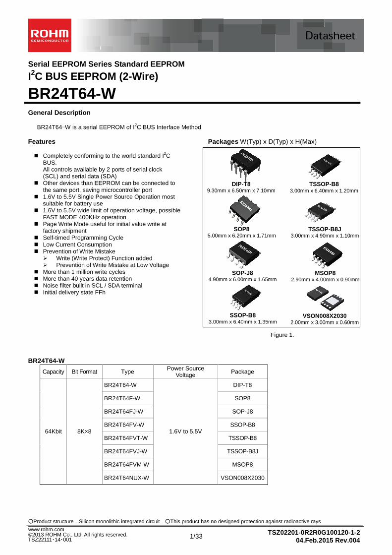
○Product structure:Silicon monolithic integrated circuit ○This product has no designed protection against radioactive rays 1/33 TSZ02201-0R2R0G100120-1-2 04.Feb.2015 Rev.004 ©2013 ROHM Co., Ltd. All rights reserved. TSZ22111・14・001 www.rohm.com Serial EEPROM Series Standard EEPROM I 2 C BUS EEPROM (2-Wire) BR24T64-W General Description BR24T64-W is a serial EEPROM of I 2 C BUS Interface Method Features Completely conforming to the world standard I 2 C BUS. All controls available by 2 ports of serial clock (SCL) and serial data (SDA) Other devices than EEPROM can be connected to the same port, saving microcontroller port 1.6V to 5.5V Single Power Source Operation most suitable for battery use 1.6V to 5.5V wide limit of operation voltage, possible FAST MODE 400KHz operation Page Write Mode useful for initial value write at factory shipment Self-timed Programming Cycle Low Current Consumption Prevention of Write Mistake Write (Write Protect) Function added Prevention of Write Mistake at Low Voltage More than 1 million write cycles More than 40 years data retention Noise filter built in SCL / SDA terminal Initial delivery state FFh Packages W(Typ) x D(Typ) x H(Max) BR24T64-W Capacity Bit Format Type Power Source Voltage Package 64Kbit 8K×8 BR24T64-W 1.6V to 5.5V DIP-T8 BR24T64F-W SOP8 BR24T64FJ-W SOP-J8 BR24T64FV-W SSOP-B8 BR24T64FVT-W TSSOP-B8 BR24T64FVJ-W TSSOP-B8J BR24T64FVM-W MSOP8 BR24T64NUX-W VSON008X2030 Figure 1. SOP8 5.00mm x 6.20mm x 1.71mm SOP-J8 4.90mm x 6.00mm x 1.65mm VSON008X2030 2.00mm x 3.00mm x 0.60mm TSSOP-B8 3.00mm x 6.40mm x 1.20mm DIP-T8 9.30mm x 6.50mm x 7.10mm TSSOP-B8J 3.00mm x 4.90mm x 1.10mm MSOP8 2.90mm x 4.00mm x 0.90mm SSOP-B8 3.00mm x 6.40mm x 1.35mm

Welcome message from author
This document is posted to help you gain knowledge. Please leave a comment to let me know what you think about it! Share it to your friends and learn new things together.
Transcript
Datasheet
Product structure:Silicon monolithic integrated circuit This product has no designed protection against radioactive rays
1/33 TSZ02201-0R2R0G100120-1-2
04.Feb.2015 Rev.004
©2013 ROHM Co., Ltd. All rights reserved. TSZ22111・14・001
www.rohm.com
Serial EEPROM Series Standard EEPROM
I2C BUS EEPROM (2-Wire)
BR24T64-W General Description
BR24T64-W is a serial EEPROM of I2C BUS Interface Method
Features
Completely conforming to the world standard I2C BUS.
All controls available by 2 ports of serial clock (SCL) and serial data (SDA)
Other devices than EEPROM can be connected to the same port, saving microcontroller port
1.6V to 5.5V Single Power Source Operation most suitable for battery use
1.6V to 5.5V wide limit of operation voltage, possible FAST MODE 400KHz operation
Page Write Mode useful for initial value write at factory shipment
Self-timed Programming Cycle Low Current Consumption Prevention of Write Mistake
Write (Write Protect) Function added Prevention of Write Mistake at Low Voltage
More than 1 million write cycles More than 40 years data retention Noise filter built in SCL / SDA terminal Initial delivery state FFh
Packages W(Typ) x D(Typ) x H(Max)
BR24T64-W
Capacity Bit Format Type Power Source Voltage Package
64Kbit 8K×8
BR24T64-W
1.6V to 5.5V
DIP-T8
BR24T64F-W SOP8
BR24T64FJ-W SOP-J8
BR24T64FV-W SSOP-B8
BR24T64FVT-W TSSOP-B8
BR24T64FVJ-W TSSOP-B8J
BR24T64FVM-W MSOP8
BR24T64NUX-W VSON008X2030
Figure 1.
SOP8 5.00mm x 6.20mm x 1.71mm
SOP-J8 4.90mm x 6.00mm x 1.65mm
VSON008X2030 2.00mm x 3.00mm x 0.60mm
TSSOP-B8 3.00mm x 6.40mm x 1.20mm
DIP-T8 9.30mm x 6.50mm x 7.10mm
TSSOP-B8J 3.00mm x 4.90mm x 1.10mm
MSOP8 2.90mm x 4.00mm x 0.90mm
SSOP-B8 3.00mm x 6.40mm x 1.35mm
Datasheet
2/33
BR24T64-W
TSZ02201-0R2R0G100120-1-2 04.Feb.2015 Rev.004
©2013 ROHM Co., Ltd. All rights reserved. TSZ22111・15・001
www.rohm.com
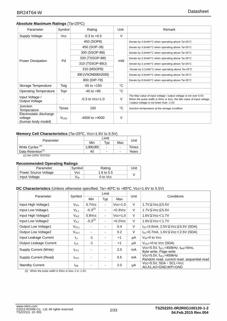
Absolute Maximum Ratings (Ta=25ºC)
Parameter Symbol Rating Unit Remark
Supply Voltage Vcc -0.3 to +6.5 V
Power Dissipation Pd
450 (SOP8)
mW
Derate by 4.5mW/°C when operating above Ta=25°C
450 (SOP-J8) Derate by 4.5mW/°C when operating above Ta=25°C
300 (SSOP-B8) Derate by 3.0mW/°C when operating above Ta=25°C
330 (TSSOP-B8) Derate by 3.3mW/°C when operating above Ta=25°C
310 (TSSOP-B8J) Derate by 3.1mW/°C when operating above Ta=25°C
310 (MSOP8) Derate by 3.1mW/°C when operating above Ta=25°C
300 (VSON008X2030) Derate by 3.0mW/°C when operating above Ta=25°C
800 (DIP-T8) Derate by 8.0mW/°C when operating above Ta=25°C
Storage Temperature Tstg -65 to +150 °C
Operating Temperature Topr -40 to +85 °C
Input Voltage / Output Voltage ‐ -0.3 to Vcc+1.0 V
The Max value of input voltage / output voltage is not over 6.5V. When the pulse width is 50ns or less, the Min value of input voltage / output voltage is not lower than -1.0V.
Junction Temperature Tjmax 150 °C Junction temperature at the storage condition
Electrostatic discharge voltage (human body model)
VESD -4000 to +4000 V
Memory Cell Characteristics (Ta=25ºC, Vcc=1.6V to 5.5V)
Parameter Limit
Unit Min Typ Max
Write Cycles (1) 1,000,000 - - Times Data Retention(1) 40 - - Years
(1) Not 100% TESTED
Recommended Operating Ratings
Parameter Symbol Rating Unit Power Source Voltage Vcc 1.6 to 5.5
V Input Voltage VIN 0 to Vcc
DC Characteristics (Unless otherwise specified, Ta=-40ºC to +85ºC, Vcc=1.6V to 5.5V)
Parameter Symbol Limit
Unit Conditions Min Typ Max
Input High Voltage1 VIH1 0.7Vcc - Vcc+1.0 V 1.7V≦Vcc≦5.5V
Input Low Voltage1 VIL1 -0.3(2) - +0.3Vcc V 1.7V≦Vcc≦5.5V
Input High Voltage2 VIH2 0.8Vcc - Vcc+1.0 V 1.6V≦Vcc<1.7V
Input Low Voltage2 VIL2 -0.3(2) - +0.2Vcc V 1.6V≦Vcc<1.7V
Output Low Voltage1 VOL1 - - 0.4 V IOL=3.0mA, 2.5V≦Vcc≦5.5V (SDA)
Output Low Voltage2 VOL2 - - 0.2 V IOL=0.7mA, 1.6V≦Vcc<2.5V (SDA)
Input Leakage Current ILI -1 - +1 µA VIN=0 to Vcc
Output Leakage Current ILO -1 - +1 µA VOUT=0 to Vcc (SDA)
Supply Current (Write) ICC1 - - 2.0 mA Vcc=5.5V, fSCL=400kHz, tWR=5ms, Byte write, Page write
Supply Current (Read) ICC2 - - 0.5 mA Vcc=5.5V, fSCL=400kHz Random read, current read, sequential read
Standby Current ISB - - 2.0 µA Vcc=5.5V, SDA・SCL=Vcc A0,A1,A2=GND,WP=GND
(2) When the pulse width is 50ns or less, it is -1.0V.

Datasheet
3/33
BR24T64-W
TSZ02201-0R2R0G100120-1-2 04.Feb.2015 Rev.004
©2013 ROHM Co., Ltd. All rights reserved. TSZ22111・15・001
www.rohm.com
AC Characteristics (Unless otherwise specified, Ta=-40ºC to +85ºC, Vcc=1.6V to 5.5V)
Parameter Symbol Limit
Unit Min Typ Max
Clock Frequency fSCL - - 400 kHz
Data Clock High Period tHIGH 0.6 - - µs
Data Clock Low Period tLOW 1.2 - - µs
SDA,SCL(INPUT) Rise Time (1) tR - - 1.0 µs
SDA,SCL (INPUT)Fall Time (1) tF1 - - 1.0 µs
SDA(OUTPUT)Fall Time (1) tF2 - - 0.3 µs
Start Condition Hold Time tHD:STA 0.6 - - µs
Start Condition Setup Time tSU:STA 0.6 - - µs
Input Data Hold Time tHD:DAT 0 - - ns
Input Data Setup Time tSU:DAT 100 - - ns
Output Data Delay Time tPD 0.1 - 0.9 µs
Output Data Hold Time tDH 0.1 - - µs
Stop Condition Setup Time tSU:STO 0.6 - - µs
Bus Free Time tBUF 1.2 - - µs
Write Cycle Time tWR - - 5 ms
Noise Spike Width (SDA and SCL) tI - - 0.1 µs
WP Hold Time tHD:WP 1.0 - - µs
WP Setup Time tSU:WP 0.1 - - µs
WP High Period tHIGH:WP 1.0 - - µs (1) Not 100% TESTED. Condition Input Data Level:VIL=0.2×Vcc VIH=0.8×Vcc Input Data Timing Reference Level: 0.3×Vcc/0.7×Vcc Output Data Timing Reference Level: 0.3×Vcc/0.7×Vcc Rise/Fall Time : ≦20ns
Serial Input / Output Timing
Input read at the rise edge of SCL Data output in sync with the fall of SCL
Figure 2-(a). Serial Input / Output Timing
Figure 2-(b). Start-Stop Bit Timing
Figure 2-(c). Write Cycle Timing
Figure 2-(d). WP Timing at Write Execution
Figure 2-(e). WP Timing at Write Cancel
70% 70%
tSU:STA tHD:STA
START CONDITION
tSU:STO
STOP CONDITION
30%30%
70%
70%
D0 ACK
tWRwrite data
(n-th address)START CONDITIONSTOP CONDITION
70%70%
DATA(1)
D0 ACKD1
DATA(n)
ACK
tWR
30%
70%
STOP CONDITION
tHD:WPtSU:WP
30%
70%
DATA(1)
D0D1 ACK
DATA(n)
ACK
tHIGH:WP
70% 70%
tWR
70%
SCL
SDA(入力)
SDA(出力)
tR tF1 tHIGH
tSU:DATtLOW
tHD:DAT
tDHtPDtBUF
tHD:STA
70%
30%
70%
70%
30%
70% 70%
30% 30%
70% 70%
30%
70% 70%
70%
70%30%
30%30% 30%
tF2
(INPUT)
(OUTPUT)
Datasheet
4/33
BR24T64-W
TSZ02201-0R2R0G100120-1-2 04.Feb.2015 Rev.004
©2013 ROHM Co., Ltd. All rights reserved. TSZ22111・15・001
www.rohm.com
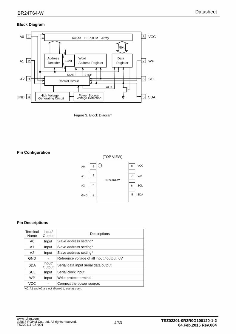
Block Diagram
Figure 3. Block Diagram Pin Configuration (TOP VIEW) Pin Descriptions
Terminal Name
Input/ Output Descriptions
A0 Input Slave address setting*
A1 Input Slave address setting*
A2 Input Slave address setting*
GND - Reference voltage of all input / output, 0V
SDA Input/ Output Serial data input serial data output
SCL Input Serial clock input
WP Input Write protect terminal
VCC - Connect the power source. *A0, A1 and A2 are not allowed to use as open.
8
7
6
5 4
3
2
1
SDA
SCL
WP
V CC
GND
A2
A1
A0
Address
Decoder Word
Address Register Data
Register
Control Circuit
High Voltage Generating Circuit
Power Source Voltage Detection
8bit
ACK
START STOP
13bit
64Kbit EEPROM Array
2
5
6
VCC
SCL
GND
BR24T64-W
1
3
4
7
8
WP
SDA
A2
A1
A0
Datasheet
5/33
BR24T64-W
TSZ02201-0R2R0G100120-1-2 04.Feb.2015 Rev.004
©2013 ROHM Co., Ltd. All rights reserved. TSZ22111・15・001
www.rohm.com
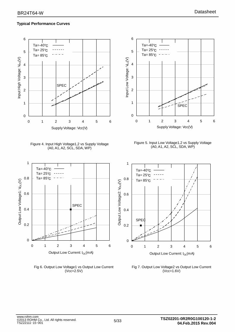
Fig 6. Output Low Voltage1 vs Output Low Current (Vcc=2.5V)
Fig 7. Output Low Voltage2 vs Output Low Current (Vcc=1.6V)
Figure 4. Input High Voltage1,2 vs Supply Voltage
(A0, A1, A2, SCL, SDA, WP)
Figure 5. Input Low Voltage1,2 vs Supply Voltage
(A0, A1, A2, SCL, SDA, WP)
Typical Performance Curves
0
0.2
0.4
0.6
0.8
1
0 1 2 3 4 5 6
Output Low Current: IOL(mA)
Ou
tpu
t Lo
w V
olta
ge1
: VO
L1(V
)
SPEC
Ta=-40Ta= 25
Ta= 85
0
1
2
3
4
5
6
0 1 2 3 4 5 6
Supply Voltage: Vcc(V)In
pu
t Lo
w V
olta
ge:
VIL
1(V
)
Ta=-40
Ta= 25
Ta= 85
SPEC
0
1
2
3
4
5
6
0 1 2 3 4 5 6
Supply Voltage: Vcc(V)
Inp
ut H
igh
Vol
tage
: VIH
1(V
)
Ta=-40
Ta= 25
Ta= 85
SPEC
0
0.2
0.4
0.6
0.8
1
0 1 2 3 4 5 6
Output Low Current: IOL(mA)
Ou
tpu
t Lo
w V
olta
ge
2: V
OL2
(V)
Ta=-40
Ta= 25
Ta= 85
SPEC
Datasheet
6/33
BR24T64-W
TSZ02201-0R2R0G100120-1-2 04.Feb.2015 Rev.004
©2013 ROHM Co., Ltd. All rights reserved. TSZ22111・15・001
www.rohm.com
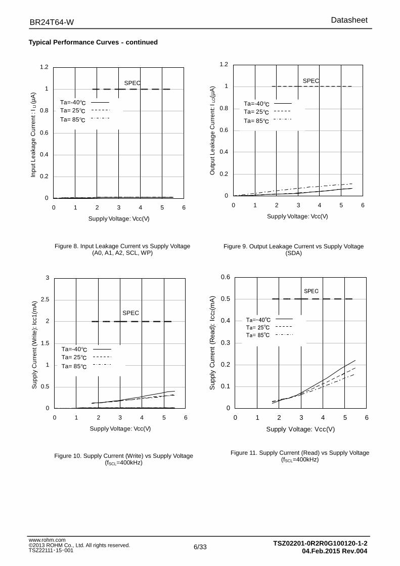
Figure 11. Supply Current (Read) vs Supply Voltage (fSCL=400kHz)
Figure 8. Input Leakage Current vs Supply Voltage (A0, A1, A2, SCL, WP)
Figure 9. Output Leakage Current vs Supply Voltage (SDA)
Figure 10. Supply Current (Write) vs Supply Voltage (fSCL=400kHz)
Typical Performance Curves‐‐‐‐continued
0
0.2
0.4
0.6
0.8
1
1.2
0 1 2 3 4 5 6
Supply Voltage: Vcc(V)
Inp
ut L
ea
kag
e C
urr
en
t : I
LI (µ
A)
Ta=-40
Ta= 25
Ta= 85
SPEC
0
0.2
0.4
0.6
0.8
1
1.2
0 1 2 3 4 5 6
Supply Voltage: Vcc(V)O
utp
ut L
ea
kag
e C
urr
en
t: I L
O(µ
A)
Ta=-40
Ta= 25
Ta= 85
SPEC
0
0.5
1
1.5
2
2.5
3
0 1 2 3 4 5 6
Supply Voltage: Vcc(V)
Sup
ply
Cu
rren
t (W
rite
): Ic
c1(m
A)
Ta=-40
Ta= 25Ta= 85
SPEC
0
0.1
0.2
0.3
0.4
0.5
0.6
0 1 2 3 4 5 6
Supply Voltage: Vcc(V)
Sup
ply
Cur
rent
(R
ead)
: Ic
c 2(m
A)
SPEC
Ta=-40
Ta= 25
Ta= 85

Datasheet
7/33
BR24T64-W
TSZ02201-0R2R0G100120-1-2 04.Feb.2015 Rev.004
©2013 ROHM Co., Ltd. All rights reserved. TSZ22111・15・001
www.rohm.com
Figure 13. Clock Frequency vs Supply Voltage
Figure 14. Data Clock High Period vs Supply Voltage
Figure 12. Standby Current vs Supply Voltage
Figure 15. Data Clock Low Period vs Supply Voltage
Typical Performance Curves‐‐‐‐continued
0.1
1
10
100
1000
10000
0 1 2 3 4 5 6
Supply Voltage: Vcc(V)
Clo
ck F
requ
en
cy: f
scl(k
Hz) SPEC
Ta=-40
Ta= 25
Ta= 85
0
0.5
1
1.5
2
2.5
0 1 2 3 4 5 6
Supply Voltage: Vcc(V)
Sta
ndb
y C
urr
ent
: I S
B (µ
A)
SPEC
Ta=-40
Ta= 25
Ta= 85
0
0.2
0.4
0.6
0.8
1
0 1 2 3 4 5 6
Supply Voltage: Vcc(V)
Da
ta C
lock
Hig
h P
erio
d :
t H
IGH(µ
s)
SPEC
Ta=-40
Ta= 25
Ta= 85
0
0.3
0.6
0.9
1.2
1.5
0 1 2 3 4 5 6
Supply Voltage: Vcc(V)
Dat
a C
lock
Low
Per
iod
: t
LOW
(µs) SPEC
Ta=-40
Ta= 25
Ta= 85
Datasheet
8/33
BR24T64-W
TSZ02201-0R2R0G100120-1-2 04.Feb.2015 Rev.004
©2013 ROHM Co., Ltd. All rights reserved. TSZ22111・15・001
www.rohm.com
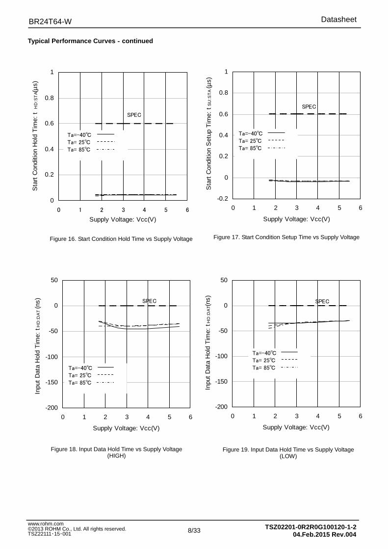
Figure 17. Start Condition Setup Time vs Supply Voltage
Figure 18. Input Data Hold Time vs Supply Voltage (HIGH)
Figure 16. Start Condition Hold Time vs Supply Voltage
Figure 19. Input Data Hold Time vs Supply Voltage (LOW)
Typical Performance Curves‐‐‐‐continued
0
0.2
0.4
0.6
0.8
1
0 1 2 3 4 5 6
Supply Voltage: Vcc(V)
Sta
rt C
ondi
tion
Hol
d T
ime:
t H
D:S
TA(
µs)
SPEC
Ta=-40
Ta= 25
Ta= 85
-0.2
0
0.2
0.4
0.6
0.8
1
0 1 2 3 4 5 6
Supply Voltage: Vcc(V)
Sta
rt C
ondi
tion
Set
up T
ime:
t S
U:S
TA
(µs)
SPEC
Ta=-40
Ta= 25
Ta= 85
-200
-150
-100
-50
0
50
0 1 2 3 4 5 6
Supply Voltage: Vcc(V)
Inpu
t D
ata
Hol
d T
ime:
t H
D:D
AT
(ns) SPEC
Ta=-40
Ta= 25
Ta= 85
-200
-150
-100
-50
0
50
0 1 2 3 4 5 6
Supply Voltage: Vcc(V)
Inp
ut D
ata
Hol
d T
ime:
t H
D:D
AT(
ns)
SPEC
Ta=-40
Ta= 25
Ta= 85
Datasheet
9/33
BR24T64-W
TSZ02201-0R2R0G100120-1-2 04.Feb.2015 Rev.004
©2013 ROHM Co., Ltd. All rights reserved. TSZ22111・15・001
www.rohm.com
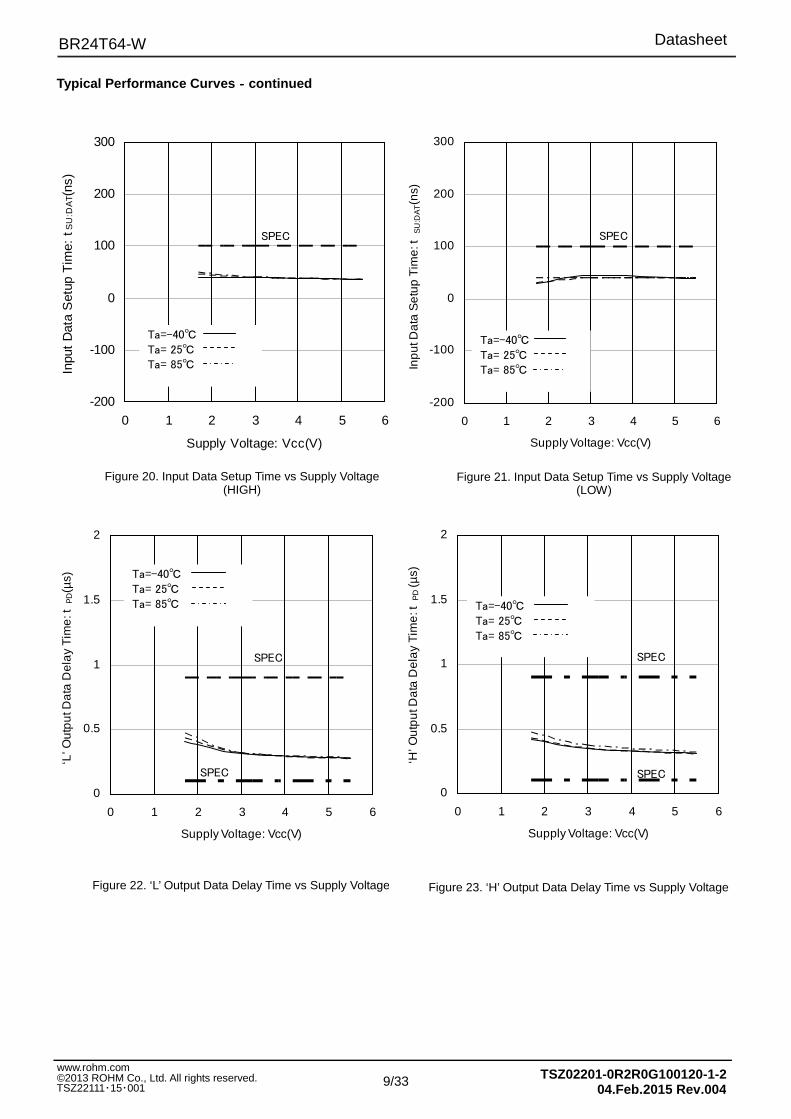
Figure 23. ‘H’ Output Data Delay Time vs Supply Voltage
Figure 21. Input Data Setup Time vs Supply Voltage (LOW)
Figure 22. ‘L’ Output Data Delay Time vs Supply Voltage
Figure 20. Input Data Setup Time vs Supply Voltage (HIGH)
Typical Performance Curves‐‐‐‐continued
-200
-100
0
100
200
300
0 1 2 3 4 5 6
Supply Voltage: Vcc(V)
Inpu
t D
ata
Set
up T
ime:
t S
U:D
AT(
ns)
SPEC
Ta=-40
Ta= 25
Ta= 85
-200
-100
0
100
200
300
0 1 2 3 4 5 6
Supply Voltage: Vcc(V)
Inp
ut D
ata
Se
tup
Tim
e: t
SU
:DA
T(n
s)
SPEC
Ta=-40
Ta= 25
Ta= 85
0
0.5
1
1.5
2
0 1 2 3 4 5 6
Supply Voltage: Vcc(V)
‘L’ O
utp
ut D
ata
Del
ay
Tim
e: t
PD(µ
s)
SPEC
SPEC
Ta=-40
Ta= 25
Ta= 85
0
0.5
1
1.5
2
0 1 2 3 4 5 6
Supply Voltage: Vcc(V)
‘H’ O
utp
ut D
ata
Del
ay
Tim
e: t
PD
(µs)
SPEC
SPEC
Ta=-40
Ta= 25
Ta= 85
Datasheet
10/33
BR24T64-W
TSZ02201-0R2R0G100120-1-2 04.Feb.2015 Rev.004
©2013 ROHM Co., Ltd. All rights reserved. TSZ22111・15・001
www.rohm.com
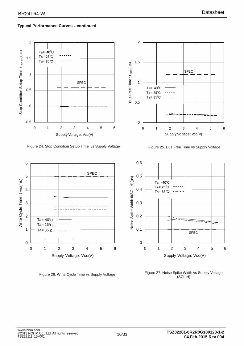
Figure 24. Stop Condition Setup Time vs Supply Voltage
Figure 27. Noise Spike Width vs Supply Voltage (SCL H)
Figure 25. Bus Free Time vs Supply Voltage
Figure 26. Write Cycle Time vs Supply Voltage
Typical Performance Curves‐‐‐‐continued
-0.5
0
0.5
1
1.5
2
0 1 2 3 4 5 6
Supply Voltage: Vcc(V)
Sto
p C
on
diti
on
Se
tup
Tim
e: t
SU
:ST
O(µ
s)
SPEC
Ta=-40
Ta= 25
Ta= 85
0
0.5
1
1.5
2
0 1 2 3 4 5 6
Supply Voltage: Vcc(V)B
us
Fre
e T
ime
: t B
UF(µ
s)
SPEC
Ta=-40
Ta= 25
Ta= 85
0
1
2
3
4
5
6
0 1 2 3 4 5 6
Supply Voltage: Vcc(V)
Writ
e C
ycle
Tim
e: t
WR(m
s)
Ta=-40Ta= 25Ta= 85
SPEC
0
0.1
0.2
0.3
0.4
0.5
0.6
0 1 2 3 4 5 6
Supply Voltage: Vcc(V)
No
ise
Sp
ike
Wid
th:tI
(SC
L H
)(µ
s)
SPEC
Ta=-40
Ta= 25
Ta= 85
Datasheet
11/33
BR24T64-W
TSZ02201-0R2R0G100120-1-2 04.Feb.2015 Rev.004
©2013 ROHM Co., Ltd. All rights reserved. TSZ22111・15・001
www.rohm.com
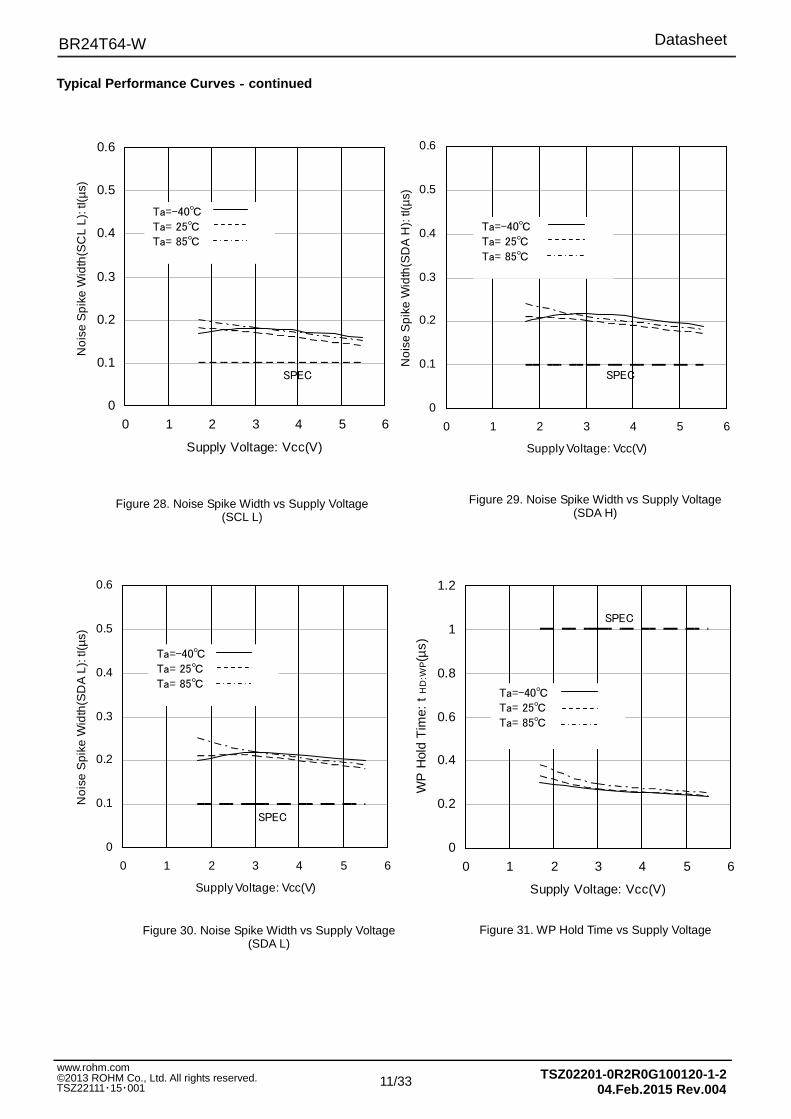
Figure 29. Noise Spike Width vs Supply Voltage (SDA H)
Figure 30. Noise Spike Width vs Supply Voltage (SDA L)
Figure 31. WP Hold Time vs Supply Voltage
Figure 28. Noise Spike Width vs Supply Voltage (SCL L)
Typical Performance Curves‐‐‐‐continued
0
0.1
0.2
0.3
0.4
0.5
0.6
0 1 2 3 4 5 6
Supply Voltage: Vcc(V)
No
ise
Sp
ike
Wid
th(S
CL
L):
tI(µ
s)
SPEC
Ta=-40
Ta= 25
Ta= 85
0
0.1
0.2
0.3
0.4
0.5
0.6
0 1 2 3 4 5 6
Supply Voltage: Vcc(V)
No
ise
Spi
ke W
idth
(SD
A L
): tI
(µs)
SPEC
Ta=-40
Ta= 25
Ta= 85
0
0.2
0.4
0.6
0.8
1
1.2
0 1 2 3 4 5 6
Supply Voltage: Vcc(V)
WP
Hol
d T
ime:
t H
D:W
P(µ
s)
SPEC
Ta=-40
Ta= 25
Ta= 85
0
0.1
0.2
0.3
0.4
0.5
0.6
0 1 2 3 4 5 6
Supply Voltage: Vcc(V)
No
ise
Sp
ike
Wid
th(S
DA
H):
tI(µ
s)
SPEC
Ta=-40
Ta= 25
Ta= 85
Datasheet
12/33
BR24T64-W
TSZ02201-0R2R0G100120-1-2 04.Feb.2015 Rev.004
©2013 ROHM Co., Ltd. All rights reserved. TSZ22111・15・001
www.rohm.com
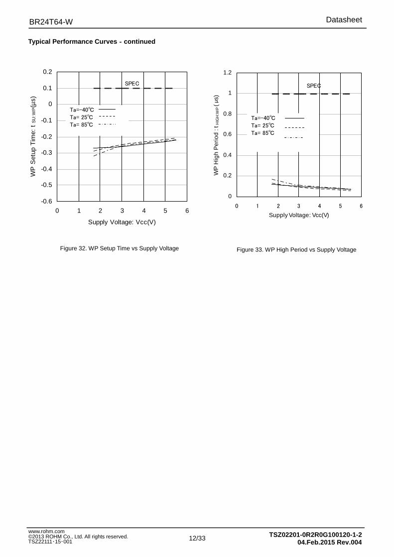
Figure 32. WP Setup Time vs Supply Voltage
Figure 33. WP High Period vs Supply Voltage
Typical Performance Curves‐‐‐‐continued
-0.6
-0.5
-0.4
-0.3
-0.2
-0.1
0
0.1
0.2
0 1 2 3 4 5 6
Supply Voltage: Vcc(V)
WP
Set
up T
ime:
t S
U:W
P(µ
s)
SPEC
Ta=-40
Ta= 25
Ta= 85
0
0.2
0.4
0.6
0.8
1
1.2
0 1 2 3 4 5 6
Supply Voltage: Vcc(V)W
P H
igh
Per
iod
: t H
IGH
:WP
( µs)
SPEC
Ta=-40
Ta= 25
Ta= 85

Datasheet
13/33
BR24T64-W
TSZ02201-0R2R0G100120-1-2 04.Feb.2015 Rev.004
©2013 ROHM Co., Ltd. All rights reserved. TSZ22111・15・001
www.rohm.com
Timing Chart
1. I2C BUS Data Communication I2C BUS data communication starts by start condition input, and ends by stop condition input. Data is always 8bit long, and acknowledge is always required after each byte. I2C BUS data communication with several devices is possible by connecting with 2 communication lines: serial data (SDA) and serial clock (SCL). Among the devices, there should be a “master” that generates clock and control communication start and end. The rest become “slave” which are controlled by an address peculiar to each device, like this EEPROM. The device that outputs data to the bus during data communication is called “transmitter”, and the device that receives data is called “receiver”..
2. Start Condition (Start Bit Recognition) (1) Before executing each command, start condition (start bit) where SDA goes from 'HIGH' down to 'LOW' when SCL is
'HIGH' is necessary. (2) This IC always detects whether SDA and SCL are in start condition (start bit) or not, therefore, unless this condition
is satisfied, any command cannot be executed. 3. Stop Condition (Stop Bit Recongition)
(1) Each command can be ended by a stop condition (stop bit) where SDA goes from 'LOW' to 'HIGH' while SCL is 'HIGH'.
4. Acknowledge (ACK) Signal
(1) The acknowledge (ACK) signal is a software rule to show whether data transfer has been made normally or not. In a master-slave communication, the device (Ex. µ-COM sends slave address input for write or read command, to this IC ) at the transmitter (sending) side releases the bus after output of 8bit data.
(2) The device (Ex. This IC receives the slave address input for write or read command from the µ-COM) at the receiver (receiving) side sets SDA 'LOW' during the 9th clock cycle, and outputs acknowledge signal (ACK signal) showing that it has received the 8bit data.
(3) This IC, after recognizing start condition and slave address (8bit), outputs acknowledge signal (ACK signal) 'LOW'. (4) After receiving 8bit data (word address and write data) during each write operation, this IC outputs acknowledge
signal (ACK signal) 'LOW'. (5) During read operation, this IC outputs 8bit data (read data) and detects acknowledge signal (ACK signal) 'LOW'.
When acknowledge signal (ACK signal) is detected, and stop condition is not sent from the master (µ-COM) side, this IC continues to output data. When acknowledge signal (ACK signal) is not detected, this IC stops data transfer, recognizes stop condition (stop bit), and ends read operation. Then this IC becomes ready for another transmission.
5. Device Addressing
(1) Slave address comes after start condition from master. (2) The significant 4 bits of slave address are used for recognizing a device type.
The device code of this IC is fixed to '1010'. (3) Next slave addresses (A2 A1 A0 --- device address) are for selecting devices, and plural ones can be used on a
same bus according to the number of device addresses. (4) The most insignificant bit ( W/R --- READ / WRITE ) of slave address is used for designating write or read
operation, and is as shown below.
Setting W/R to 0 ------- write (setting 0 to word address setting of random read)
Setting W/R to 1 ------- read
Slave Address Maximum Number of
Connected Buses
1 0 1 0 A2 A1 A0 R/W――
8
8 9 8 9 8 9
S P
condition condition
ACK STOPACKDATA DATAADDRESSSTART R/W ACK
1-7
SDA
SCL
1-7 1-7
Figure 34. Data Transfer Timing
Datasheet
14/33
BR24T64-W
TSZ02201-0R2R0G100120-1-2 04.Feb.2015 Rev.004
©2013 ROHM Co., Ltd. All rights reserved. TSZ22111・15・001
www.rohm.com
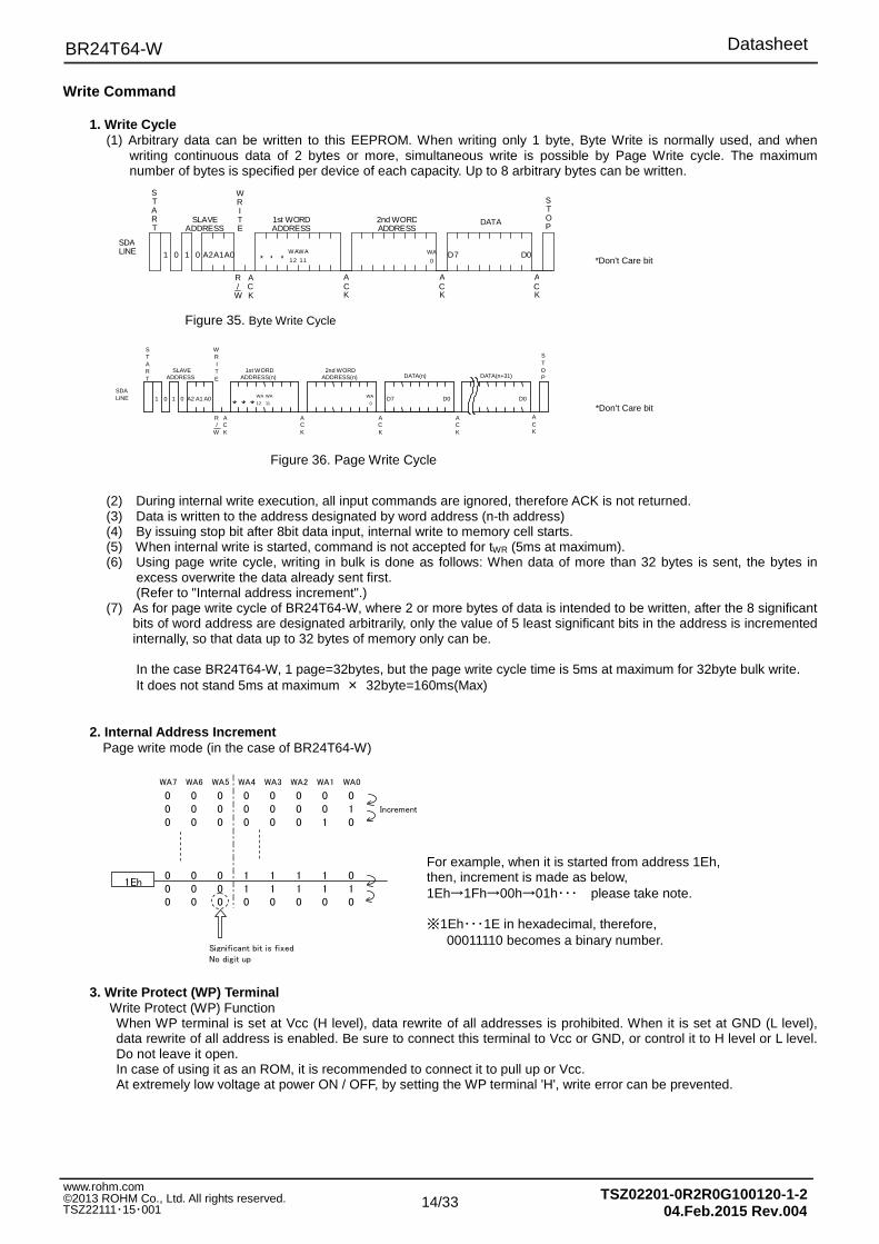
Write Command
1. Write Cycle (1) Arbitrary data can be written to this EEPROM. When writing only 1 byte, Byte Write is normally used, and when
writing continuous data of 2 bytes or more, simultaneous write is possible by Page Write cycle. The maximum number of bytes is specified per device of each capacity. Up to 8 arbitrary bytes can be written.
(2) During internal write execution, all input commands are ignored, therefore ACK is not returned. (3) Data is written to the address designated by word address (n-th address) (4) By issuing stop bit after 8bit data input, internal write to memory cell starts. (5) When internal write is started, command is not accepted for tWR (5ms at maximum). (6) Using page write cycle, writing in bulk is done as follows: When data of more than 32 bytes is sent, the bytes in
excess overwrite the data already sent first. (Refer to "Internal address increment".)
(7) As for page write cycle of BR24T64-W, where 2 or more bytes of data is intended to be written, after the 8 significant bits of word address are designated arbitrarily, only the value of 5 least significant bits in the address is incremented internally, so that data up to 32 bytes of memory only can be.
In the case BR24T64-W, 1 page=32bytes, but the page write cycle time is 5ms at maximum for 32byte bulk write. It does not stand 5ms at maximum × 32byte=160ms(Max)
2. Internal Address Increment Page write mode (in the case of BR24T64-W)
3. Write Protect (WP) Terminal Write Protect (WP) Function When WP terminal is set at Vcc (H level), data rewrite of all addresses is prohibited. When it is set at GND (L level), data rewrite of all address is enabled. Be sure to connect this terminal to Vcc or GND, or control it to H level or L level. Do not leave it open. In case of using it as an ROM, it is recommended to connect it to pull up or Vcc. At extremely low voltage at power ON / OFF, by setting the WP terminal 'H', write error can be prevented.
A1 A2 1 1 0 0
W R I T E
S T A R T
R /
W
S T O P
1st WORD ADDRESS
DATA SLAVE ADDRESS
A0 D0
A C K
SDA LINE
A C K
A C K
* W A
12
WA
11 WA
0
A C K
2nd WORD ADDRESS
D7 * * *Don't Care bit
Figure 35. Byte Write Cycle
Figure 36. Page Write Cycle
D0 D7
A
C K
2nd WORD ADDRESS(n)
WA
0 *
WA 12 WA
11
For example, when it is started from address 1Eh, then, increment is made as below, 1Eh→1Fh→00h→01h・・・ please take note. ※1Eh・・・1E in hexadecimal, therefore,
00011110 becomes a binary number.
WA7 WA6 WA5 WA4 WA3 WA2 WA1 WA0
0 0 0 0 0 0 0 0
0 0 0 0 0 0 0 1
0 0 0 0 0 0 1 0
0 0 0 1 1 1 1 0
0 0 0 1 1 1 1 1
0 0 0 0 0 0 0 0
Increment
1Eh
Significant bit is fixed.
No digit up
*Don't Care bit
W R I T E
S T A R T
R / W
A C K
S T O P
1st WORD ADDRESS(n)
SDA
LINE
A C K
A C K
DATA(n+31)
A C K
SLAVE ADDRESS
1 0
0 1 A0
A1 A2
D0
DATA(n)
* *

Datasheet
15/33
BR24T64-W
TSZ02201-0R2R0G100120-1-2 04.Feb.2015 Rev.004
©2013 ROHM Co., Ltd. All rights reserved. TSZ22111・15・001
www.rohm.com
Read Command
1. Read Cycle Read cycle is when data of EEPROM is read. Read cycle could be random read cycle or current read cycle. Random read cycle is a command to read data by designating a specific address, and is used generally. Current read cycle is a command to read data of internal address register without designating an address, and is used when to verify just after write cycle. In both the read cycles, sequential read cycle is available where the next address data can be read in succession.
(1) In random read cycle, data of designated word address can be read. (2) When the command just before current read cycle is random read cycle, current read cycle (each including
sequential read cycle), data of incremented last read address (n)-th, i.e., data of the (n+1)-th address is output. (3) When ACK signal 'LOW' after D0 is detected, and stop condition is not sent from master (µ-COM) side, the next
address data can be read in succession. (4) Read cycle is ended by stop condition where 'H' is input to ACK signal after D0 and SDA signal goes from ‘L’ to ‘H’
while SCL signal is 'H'. (5) When 'H' is not input to ACK signal after D0, sequential read gets in, and the next data is output.
Therefore, read command cycle cannot be ended. To end read command cycle, be sure to input 'H' to ACK signal after D0, and the stop condition where SDA goes from ‘L’ to ‘H’ while SCL signal is 'H'.
(6) Sequential read is ended by stop condition where 'H' is input to ACK signal after arbitrary D0 and SDA is asserted from ‘L’ to ‘H’ while SCL signal is 'H'.
Figure 37. Random Read Cycle
*Don't Care bit
Figure 38. Current Read Cycle
Figure 39. Sequential Read Cycle (in the case of current read cycle)
A2 A0 A1 A1 A2
W R I T E
S T A R T
R /
W
A C K
S T O P
1st WORD ADDRESS
(n)
SDA LINE
A C K
A C K
DATA(n)
A C K
SLAVE ADDRESS
1 0 0 1 A0 D7 D0
2nd WORD ADDRESS(n)
A C K
S T A R T
SLAVE ADDRESS
1 0 0 1
R /
W
R E A D
WA
0 * WA
12 WA
11 * *
S T A R T
S T O P
SDA LINE
A C K
DATA(n)
A C K
SLAVE ADDRESS
1 0 0 1 A0 A1 A2 D0 D7
R /
W
R E A D
R E A D
S T A R T
R /
W
A C K
S T O P DATA(n)
SDA LINE
A C K
A C K
DATA(n+x)
A C K
SLAVE ADDRESS
1 0 0 1 A0 A1 A2 D0 D7 D0 D7
Datasheet
16/33
BR24T64-W
TSZ02201-0R2R0G100120-1-2 04.Feb.2015 Rev.004
©2013 ROHM Co., Ltd. All rights reserved. TSZ22111・15・001
www.rohm.com
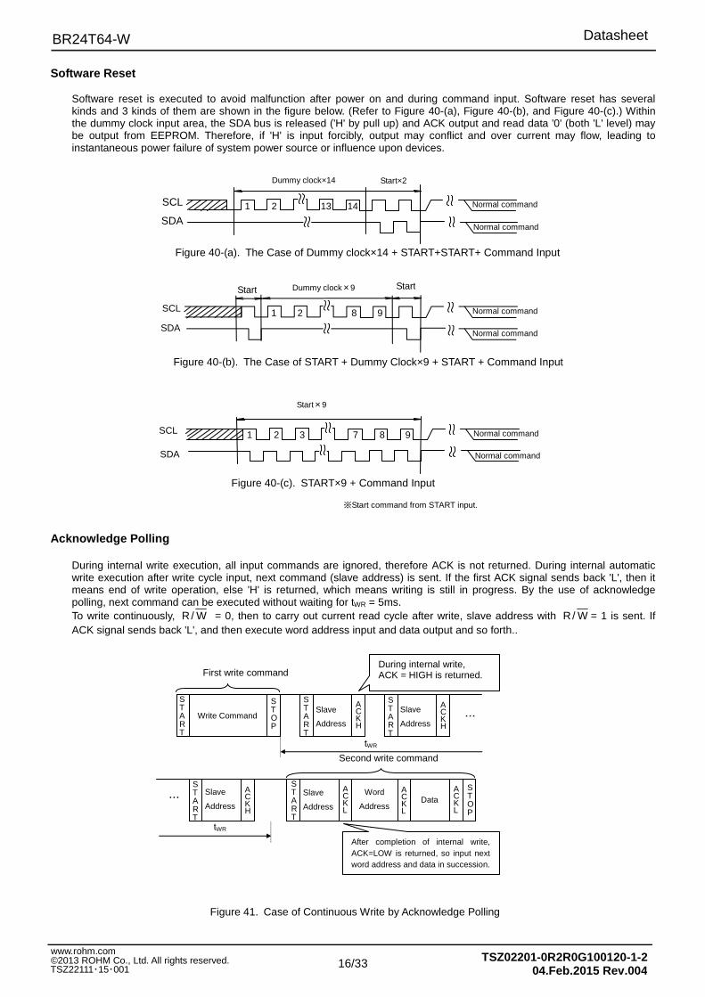
Software Reset
Software reset is executed to avoid malfunction after power on and during command input. Software reset has several kinds and 3 kinds of them are shown in the figure below. (Refer to Figure 40-(a), Figure 40-(b), and Figure 40-(c).) Within the dummy clock input area, the SDA bus is released ('H' by pull up) and ACK output and read data '0' (both 'L' level) may be output from EEPROM. Therefore, if 'H' is input forcibly, output may conflict and over current may flow, leading to instantaneous power failure of system power source or influence upon devices.
Acknowledge Polling
During internal write execution, all input commands are ignored, therefore ACK is not returned. During internal automatic write execution after write cycle input, next command (slave address) is sent. If the first ACK signal sends back 'L', then it means end of write operation, else 'H' is returned, which means writing is still in progress. By the use of acknowledge polling, next command can be executed without waiting for tWR = 5ms. To write continuously, W/R = 0, then to carry out current read cycle after write, slave address with W/R = 1 is sent. If ACK signal sends back 'L', and then execute word address input and data output and so forth..
1 2 13 14 SCL
Dummy clock×14 Start×2
SCL
Figure 40-(a). The Case of Dummy clock×14 + START+START+ Command Input
※Start command from START input.
2 1 8 9
Dummy clock×9 Start
Figure 40-(b). The Case of START + Dummy Clock×9 + START + Command Input
Start
Normal command
Normal command
Normal command
Normal command
Start×9
SDA
SDA
SCL
SD
1 2 3 8 9 7
Figure 40-(c). START×9 + Command Input
Normal command
Normal command SDA
Slave
Address
Word
Address
…
…
S T A R T
First write command
A C K H
A C K L
Slave
Address
Slave
Address
Slave
Address Data
Write Command
During internal write, ACK = HIGH is returned.
After completion of internal write, ACK=LOW is returned, so input next word address and data in succession.
tWR
tWR
Second write command
S T A R T
S T A R T
S T A R T
S T A R T
S T O P
S T O P
A C K H
A C K H
A C K L
A C K L
Figure 41. Case of Continuous Write by Acknowledge Polling
Datasheet
17/33
BR24T64-W
TSZ02201-0R2R0G100120-1-2 04.Feb.2015 Rev.004
©2013 ROHM Co., Ltd. All rights reserved. TSZ22111・15・001
www.rohm.com
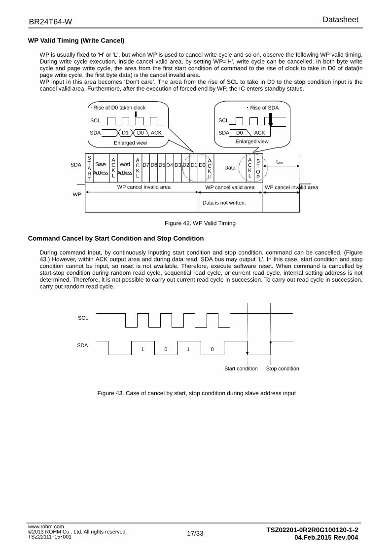
WP Valid Timing (Write Cancel)
WP is usually fixed to 'H' or 'L', but when WP is used to cancel write cycle and so on, observe the following WP valid timing. During write cycle execution, inside cancel valid area, by setting WP='H', write cycle can be cancelled. In both byte write cycle and page write cycle, the area from the first start condition of command to the rise of clock to take in D0 of data(in page write cycle, the first byte data) is the cancel invalid area. WP input in this area becomes ‘Don't care’. The area from the rise of SCL to take in D0 to the stop condition input is the cancel valid area. Furthermore, after the execution of forced end by WP, the IC enters standby status.
Command Cancel by Start Condition and Stop Condition
During command input, by continuously inputting start condition and stop condition, command can be cancelled. (Figure 43.) However, within ACK output area and during data read, SDA bus may output 'L'. In this case, start condition and stop condition cannot be input, so reset is not available. Therefore, execute software reset. When command is cancelled by start-stop condition during random read cycle, sequential read cycle, or current read cycle, internal setting address is not determined. Therefore, it is not possible to carry out current read cycle in succession. To carry out read cycle in succession, carry out random read cycle.
・Rise of D0 taken clock
SCL
D0 ACK
Enlarged view
SCL
SDA ACK D0
・Rise of SDA
SDA
WP WP cancel invalid area WP cancel valid area
Data is not written.
Figure 42. WP Valid Timing
Slave
Address
D7 D6 D5 D4 D3 D2 D1 D0 Data tWR
SDA D1
S T A R T
A C K L
A C K L
A C K L
A C K L
S T O P
Word
Address
Figure 43. Case of cancel by start, stop condition during slave address input
SCL
SDA 1 1 0 0
Start condition Stop condition
Enlarged view
WP cancel invalid area

Datasheet
18/33
BR24T64-W
TSZ02201-0R2R0G100120-1-2 04.Feb.2015 Rev.004
©2013 ROHM Co., Ltd. All rights reserved. TSZ22111・15・001
www.rohm.com
I/O Peripheral Circuit
1. Pull-up Resistance of SDA Terminal SDA is NMOS open drain, so it requires a pull up resistor. As for this resistance value (RPU), select an appropriate value from microcontroller VIL, IL, and VOL-IOL characteristics of this IC. If RPU is large, operating frequency is limited. The smaller the RPU, the larger is the supply current (Read).
2. Maximum Value of RPU
The maximum value of RPU is determined by the following factors. (1) SDA rise time to be determined by the capacitance (CBUS) of bus line and RPU of SDA should be tR or lower.
Furthermore, AC timing should be satisfied even when SDA rise time is slow. (2) The bus. electric potential A to be determined by the input current leak total (IL) of device connected to bus at
output of 'H' to the SDA line and RPU should sufficiently secure the input 'H' level (VIH) of microcontroller and EEPROM including recommended noise margin of 0.2Vcc.
VCC-ILRPU-0.2 VCC ≧ VIH Ex.) Vcc =3V IL=10µA VIH=0.7 Vcc
From (2)
≦ 30 [kΩ]
3. Minimum Value of RPU
The minimum value of RPU is determined by the following factors. (1) When IC outputs LOW, it should be satisfied that VOLMAX=0.4V and IOLMAX=3mA.
(2) VOLMAX=0.4V should secure the input 'L' level (VIL) of microcontroller and EEPROM including recommended noise
margin 0.1Vcc.
VOLMAX ≦ VIL-0.1 VCC
Ex.) VCC =3V, VOL=0.4V, IOL=3mA, microcontroller, EEPROM VIL=0.3Vcc
from (1)
≧ 867 [Ω]
And VOL=0.4 [V]
VIL=0.3×3 =0.9 [V]
Therefore, the condition (2) is satisfied.
4. Pull-up Resistance of SCL Terminal When SCL control is made at the CMOS output port, there is no need for a pull up resistor. But when there is a time where SCL becomes 'Hi-Z', add a pull up resistor. As for the pull up resistor value, one of several kΩ to several ten kΩ is recommended in consideration of drive performance of output port of microcontroller.
Figure 44. I/O Circuit Diagram
Microcontroller
RPU
A SDA terminal
IL IL
Bus line capacity CBUS
BR24TXX ∴ RPU≦
0.8Vcc-VIH IL
RPU≦ 0.8×3-0.7×3
10×10-6
∴ RPU≧
Vcc-VOL RPU ≦IOL
Vcc-VOL IOL
RPU≧
3-0.4 3×10-
3
Datasheet
19/33
BR24T64-W
TSZ02201-0R2R0G100120-1-2 04.Feb.2015 Rev.004
©2013 ROHM Co., Ltd. All rights reserved. TSZ22111・15・001
www.rohm.com
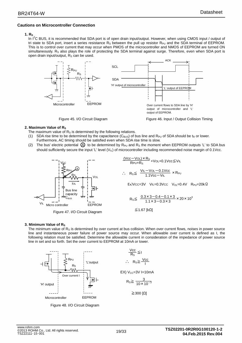
Cautions on Microcontroller Connection
1. RS In I2C BUS, it is recommended that SDA port is of open drain input/output. However, when using CMOS input / output of tri state to SDA port, insert a series resistance RS between the pull up resistor RPU and the SDA terminal of EEPROM. This is to control over current that may occur when PMOS of the microcontroller and NMOS of EEPROM are turned ON simultaneously. RS also plays the role of protecting the SDA terminal against surge. Therefore, even when SDA port is open drain input/output, RS can be used.
2. Maximum Value of RS The maximum value of RS is determined by the following relations. (1) SDA rise time to be determined by the capacitance (CBUS) of bus line and RPU of SDA should be tR or lower.
Furthermore, AC timing should be satisfied even when SDA rise time is slow. (2) The bus’ electric potential A to be determined by RPU and RS the moment when EEPROM outputs 'L' to SDA bus
should sufficiently secure the input 'L' level (VIL) of microcontroller including recommended noise margin of 0.1Vcc.
Ex)VCC=3V VIL=0.3VCC VOL=0.4V RPU=20kΩ
3. Minimum Value of RS
The minimum value of RS is determined by over current at bus collision. When over current flows, noises in power source line and instantaneous power failure of power source may occur. When allowable over current is defined as I, the following relation must be satisfied. Determine the allowable current in consideration of the impedance of power source line in set and so forth. Set the over current to EEPROM at 10mA or lower.
EX) VCC=3V I=10mA
(Vcc-VOL)×RS RPU+RS
RPU
Microcontroller
RS
EEPROM
Figure 45. I/O Circuit Diagram Figure 46. Input / Output Collision Timing
ACK
'L' output of EEPROM 'H' output of microcontroller
Over current flows to SDA line by 'H' output of microcontroller and 'L' output of EEPROM.
SCL
SDA
Microcontroller EEPROM
'L'output R S
R PU
'H' output
Over current I
Figure 48. I/O Circuit Diagram
Figure 47. I/O Circuit Diagram
RPU
Micro controller
RS
EEPROM
IOL
A
Bus line capacity CBUS
VOL
VCC
VIL
+VOL+0.1Vcc≦VIL
∴ RS≦ ×RPU VIL-VOL-0.1Vcc 1.1Vcc-VIL
≦1.67 [kΩ]
RS≦ 0.3×3-0.4-0.1×3
1.1×3-0.3×3 ×20×103
RS≧ 3
10×10-3
≧300 [Ω]
Vcc RS ≦I
∴ RS≧ Vcc
I

Datasheet
20/33
BR24T64-W
TSZ02201-0R2R0G100120-1-2 04.Feb.2015 Rev.004
©2013 ROHM Co., Ltd. All rights reserved. TSZ22111・15・001
www.rohm.com
I/O Equivalence Circuit
1. Input (A0, A1, A2, SCL, WP)
2. Input / Output (SDA)
Figure 49. Input Pin Circuit Diagram
Figure 50. Input / Output Pin Circuit Diagram
Datasheet
21/33
BR24T64-W
TSZ02201-0R2R0G100120-1-2 04.Feb.2015 Rev.004
©2013 ROHM Co., Ltd. All rights reserved. TSZ22111・15・001
www.rohm.com
Power-Up / Down Conditions
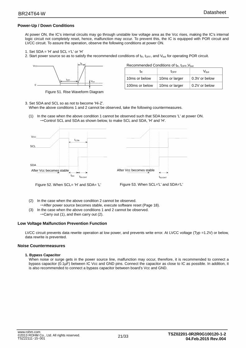
At power ON, the IC’s internal circuits may go through unstable low voltage area as the Vcc rises, making the IC’s internal logic circuit not completely reset, hence, malfunction may occur. To prevent this, the IC is equipped with POR circuit and LVCC circuit. To assure the operation, observe the following conditions at power ON.
1. Set SDA = 'H' and SCL ='L' or 'H’ 2. Start power source so as to satisfy the recommended conditions of tR, tOFF, and Vbot for operating POR circuit.
tOFF
tR
Vbot 0
VCC
3. Set SDA and SCL so as not to become 'Hi-Z'. When the above conditions 1 and 2 cannot be observed, take the following countermeasures.
(1) In the case when the above condition 1 cannot be observed such that SDA becomes 'L' at power ON. →Control SCL and SDA as shown below, to make SCL and SDA, 'H' and 'H'.
(2) In the case when the above condition 2 cannot be observed. →After power source becomes stable, execute software reset (Page 18). (3) In the case when the above conditions 1 and 2 cannot be observed. →Carry out (1), and then carry out (2).
Low Voltage Malfunction Prevention Function
LVCC circuit prevents data rewrite operation at low power, and prevents write error. At LVCC voltage (Typ =1.2V) or below, data rewrite is prevented.
Noise Countermeasures
1. Bypass Capacitor When noise or surge gets in the power source line, malfunction may occur, therefore, it is recommended to connect a bypass capacitor (0.1µF) between IC Vcc and GND pins. Connect the capacitor as close to IC as possible. In addition, it is also recommended to connect a bypass capacitor between board’s Vcc and GND.
Recommended Conditions of tR, tOFF,Vbot
tR tOFF Vbot
10ms or below 10ms or larger 0.3V or below
100ms or below 10ms or larger 0.2V or below
Figure 51. Rise Waveform Diagram
Figure 52. When SCL= 'H' and SDA= 'L' Figure 53. When SCL='L' and SDA='L'
tLOW
tSU:DAT tDH
After Vcc becomes stable
SCL
V CC
SDA
tSU:DAT
After Vcc becomes stable

Datasheet
22/33
BR24T64-W
TSZ02201-0R2R0G100120-1-2 04.Feb.2015 Rev.004
©2013 ROHM Co., Ltd. All rights reserved. TSZ22111・15・001
www.rohm.com
Operational Notes
1. Described numeric values and data are design representative values only, and the values are not guaranteed. 2. We believe that the application circuit examples in this document are recommendable. However, in actual use, confirm
characteristics further sufficiently. If changing the fixed number of external parts is desired, make your decision with sufficient margin in consideration of static characteristics, transient characteristics, and fluctuations of external parts and our LSI.
3. Absolute maximum ratings
If the absolute maximum ratings such as supply voltage, operating temperature range, and so on are exceeded, LSI may be destroyed. Do not supply voltage or subject the IC to temperatures exceeding the absolute maximum ratings. In the case of fear of exceeding the absolute maximum ratings, take physical safety countermeasures such as adding fuses, and see to it that conditions exceeding the absolute maximum ratings should not be supplied to the LSI.
4. GND electric potential
Set the voltage of GND terminal lowest at any operating condition. Make sure that each terminal voltage is not lower than that of GND terminal.
5. Thermal design
Use a thermal design that allows for a sufficient margin by taking into account the permissible power dissipation (Pd) in actual operating conditions.
6. Short between pins and mounting errors
Be careful when mounting the IC on printed circuit boards. The IC may be damaged if it is mounted in a wrong orientation or if pins are shorted together. Short circuit may be caused by conductive particles caught between the pins.
7. Operating the IC in the presence of strong electromagnetic field may cause malfunction, therefore, evaluate design
sufficiently.

Datasheet
23/33
BR24T64-W
TSZ02201-0R2R0G100120-1-2 04.Feb.2015 Rev.004
©2013 ROHM Co., Ltd. All rights reserved. TSZ22111・15・001
www.rohm.com
Part Numbering
B R 2 4 T 6 4 x x x - W x x
BUS Type 24:I2C Operating Temperature/ Power Source Voltage
-40ºC to+85ºC/ 1.6V to 5.5V
Capacity
64=64K Package
Blank :DIP-T8
F :SOP8
FJ :SOP-J8
FV : SSOP-B8
FVT : TSSOP-B8
FVJ : TSSOP-B8J
FVM : MSOP8
NUX : VSON008X2030 Double Cell
Packaging and Forming Specification
E2 : Embossed tape and reel (SOP8,SOP-J8, SSOP-B8,TSSOP-B8, TSSOP-B8J)
TR : Embossed tape and reel (MSOP8, VSON008X2030) None : Tube (DIP-T8)
Datasheet
24/33
BR24T64-W
TSZ02201-0R2R0G100120-1-2 04.Feb.2015 Rev.004
©2013 ROHM Co., Ltd. All rights reserved. TSZ22111・15・001
www.rohm.com
Physical Dimensions Tape and Reel Information
∗ Order quantity needs to be multiple of the minimum quantity.
<Tape and Reel information>
TubeContainer
Quantity
Direction of feed
2000pcs
Direction of products is fixed in a container tube
(Unit : mm)
DIP-T8
0°−15°
7.62
0.3±0.1
9.3±0.3
6.5±
0.3
8 5
1 4
0.51
Min
.
3.4±
0.3
3.2±
0.2
2.54 0.5±0.1
Datasheet
25/33
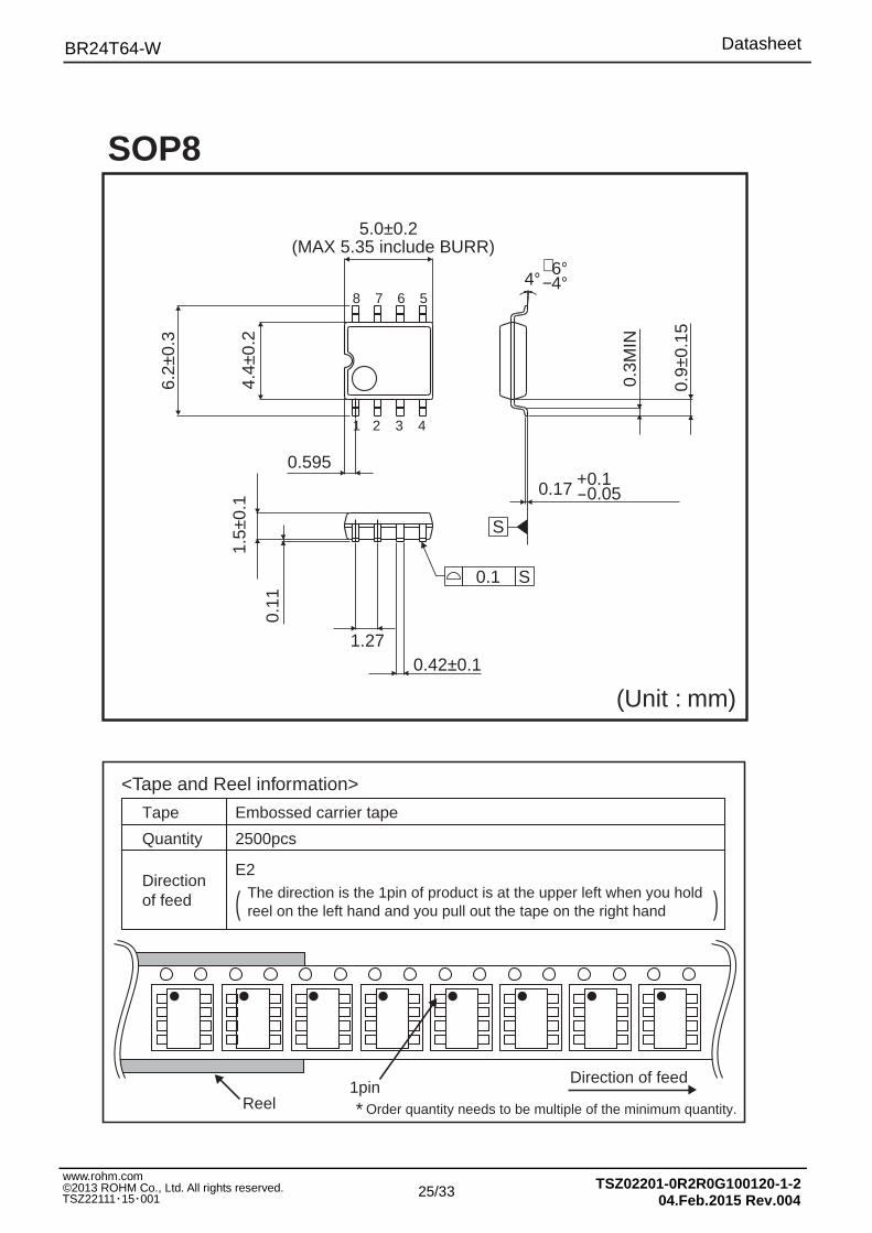
BR24T64-W
TSZ02201-0R2R0G100120-1-2 04.Feb.2015 Rev.004
©2013 ROHM Co., Ltd. All rights reserved. TSZ22111・15・001
www.rohm.com
∗ Order quantity needs to be multiple of the minimum quantity.
<Tape and Reel information>
Embossed carrier tapeTape
Quantity
Direction of feed The direction is the 1pin of product is at the upper left when you hold
reel on the left hand and you pull out the tape on the right hand
2500pcs
E2
( )
Direction of feed
Reel1pin
(Unit : mm)
SOP8
0.9±
0.15
0.3M
IN
4°+6°−4°
0.17 +0.1-0.05
0.595
6
43
8
2
5
1
7
5.0±0.2
6.2±
0.3
4.4±
0.2
(MAX 5.35 include BURR)
1.27
0.11
0.42±0.1
1.5±
0.1
S
0.1 S
Datasheet
26/33
BR24T64-W
TSZ02201-0R2R0G100120-1-2 04.Feb.2015 Rev.004
©2013 ROHM Co., Ltd. All rights reserved. TSZ22111・15・001
www.rohm.com
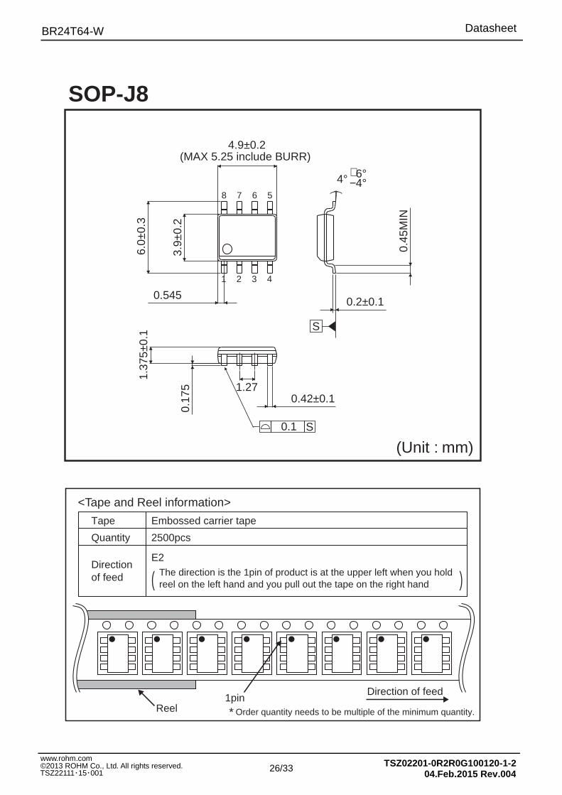
∗ Order quantity needs to be multiple of the minimum quantity.
<Tape and Reel information>
Embossed carrier tapeTape
Quantity
Direction of feed The direction is the 1pin of product is at the upper left when you hold
reel on the left hand and you pull out the tape on the right hand
2500pcs
E2
( )
Direction of feed
Reel1pin
(Unit : mm)
SOP-J8
4° +6°−4°
0.2±0.1
0.45
MIN
2 3 4
5678
1
4.9±0.2
0.545
3.9±
0.2
6.0±
0.3
(MAX 5.25 include BURR)
0.42±0.11.27
0.17
5
1.37
5±0.
1
0.1 S
S
Datasheet
27/33
BR24T64-W
TSZ02201-0R2R0G100120-1-2 04.Feb.2015 Rev.004
©2013 ROHM Co., Ltd. All rights reserved. TSZ22111・15・001
www.rohm.com
∗ Order quantity needs to be multiple of the minimum quantity.
<Tape and Reel information>
Embossed carrier tapeTape
Quantity
Direction of feed The direction is the 1pin of product is at the upper left when you hold
reel on the left hand and you pull out the tape on the right hand
2500pcs
E2
( )
Direction of feed
Reel1pin
(Unit : mm)
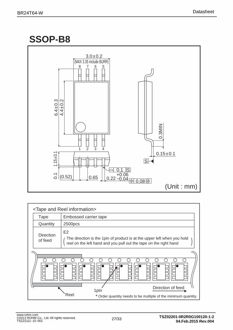
SSOP-B8
0.08 M
0.3M
IN
0.65(0.52)
3.0±0.2
0.15±0.1
(MAX 3.35 include BURR)
S
S0.1
1 2 3 4
5678
0.22
6.4
±0.3
4.4
±0.2
+0.06−0.040.
11.
15±0
.1
Datasheet
28/33
BR24T64-W
TSZ02201-0R2R0G100120-1-2 04.Feb.2015 Rev.004
©2013 ROHM Co., Ltd. All rights reserved. TSZ22111・15・001
www.rohm.com
Direction of feed
Reel ∗ Order quantity needs to be multiple of the minimum quantity.
<Tape and Reel information>
Embossed carrier tapeTape
Quantity
Direction of feed
The direction is the 1pin of product is at the upper left when you hold reel on the left hand and you pull out the tape on the right hand
3000pcs
E2
( )
1pin
(Unit : mm)
TSSOP-B8
0.08 S
0.08 M
4 ± 4
2 3 4
8 7 6 5
1
1.0
±0.0
5
1PIN MARK0.525
0.245+0.05−0.04
0.65
0.145+0.05−0.03
0.1
±0.0
51.2M
AX
3.0±0.1
4.4
±0.1
6.4
±0.2
0.5
±0.1
5
1.0
±0.2
(MAX 3.35 include BURR)
S
Datasheet
29/33
BR24T64-W
TSZ02201-0R2R0G100120-1-2 04.Feb.2015 Rev.004
©2013 ROHM Co., Ltd. All rights reserved. TSZ22111・15・001
www.rohm.com
Direction of feed
Reel ∗ Order quantity needs to be multiple of the minimum quantity.
<Tape and Reel information>
Embossed carrier tapeTape
Quantity
Direction of feed
The direction is the 1pin of product is at the upper left when you hold reel on the left hand and you pull out the tape on the right hand
2500pcs
E2
( )
1pin
(Unit : mm)
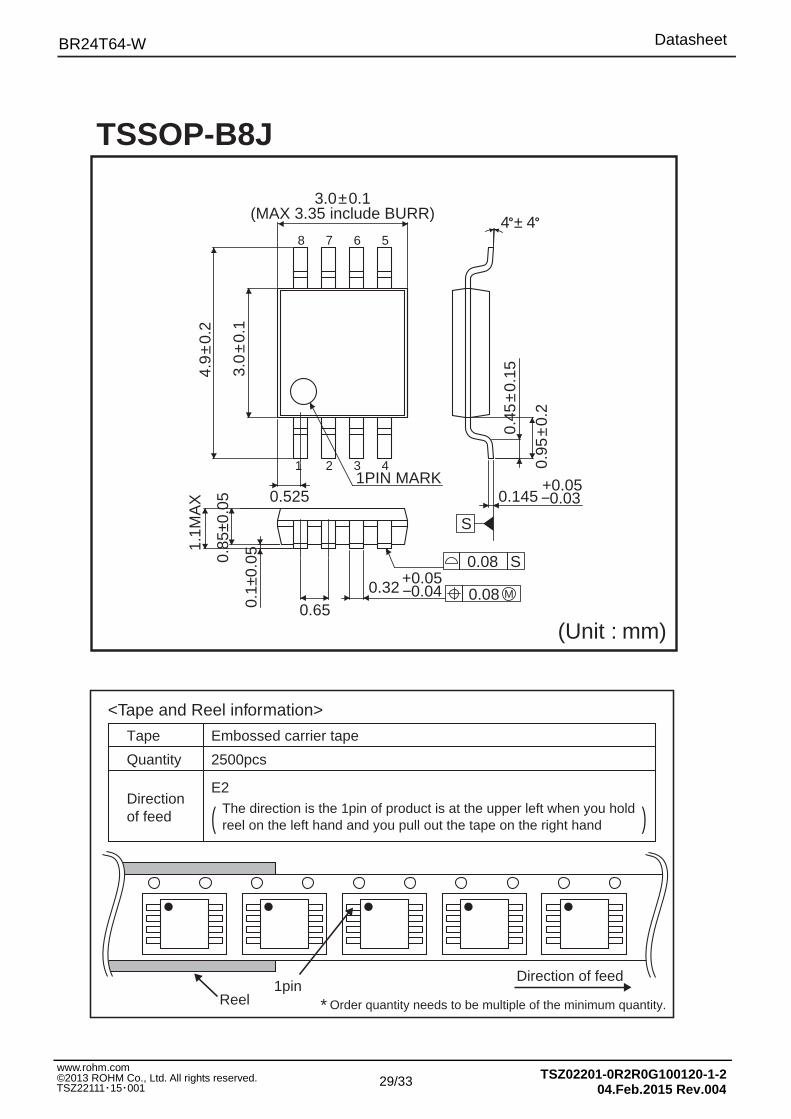
TSSOP-B8J
0.08 M
0.08 S
S
4 ± 4(MAX 3.35 include BURR)
578
1 2 3 4
63.
0±0
.1
1PIN MARK
0.95
±0.2
0.65
4.9
±0.2
3.0±0.1
0.45
±0.1
5
0.85
±0.0
5 0.145
0.1±
0.05
0.32
0.525
1.1M
AX
+0.05−0.03
+0.05−0.04

Datasheet
30/33
BR24T64-W
TSZ02201-0R2R0G100120-1-2 04.Feb.2015 Rev.004
©2013 ROHM Co., Ltd. All rights reserved. TSZ22111・15・001
www.rohm.com
Direction of feed
Reel ∗ Order quantity needs to be multiple of the minimum quantity.
<Tape and Reel information>
Embossed carrier tapeTape
Quantity
Direction of feed
The direction is the 1pin of product is at the upper right when you hold reel on the left hand and you pull out the tape on the right hand
3000pcs
TR
( )1pin
(Unit : mm)
MSOP8
0.08 S
S
4.0±
0.2
8
3
2.8±
0.1
1
6
2.9±0.1
0.475
4
57
(MAX 3.25 include BURR)
2
1PIN MARK
0.9M
AX
0.75
±0.0
5
0.650.08
±0.0
5 0.22+0.05−0.04
0.6±
0.2
0.29
±0.1
5
0.145+0.05−0.03
4°+6°−4°
Datasheet
31/33
BR24T64-W
TSZ02201-0R2R0G100120-1-2 04.Feb.2015 Rev.004
©2013 ROHM Co., Ltd. All rights reserved. TSZ22111・15・001
www.rohm.com
∗ Order quantity needs to be multiple of the minimum quantity.
<Tape and Reel information>
Embossed carrier tapeTape
Quantity
Direction of feed The direction is the 1pin of product is at the upper right when you hold
reel on the left hand and you pull out the tape on the right hand
4000pcs
TR
( )
Direction of feed
Reel1pin
(Unit : mm)
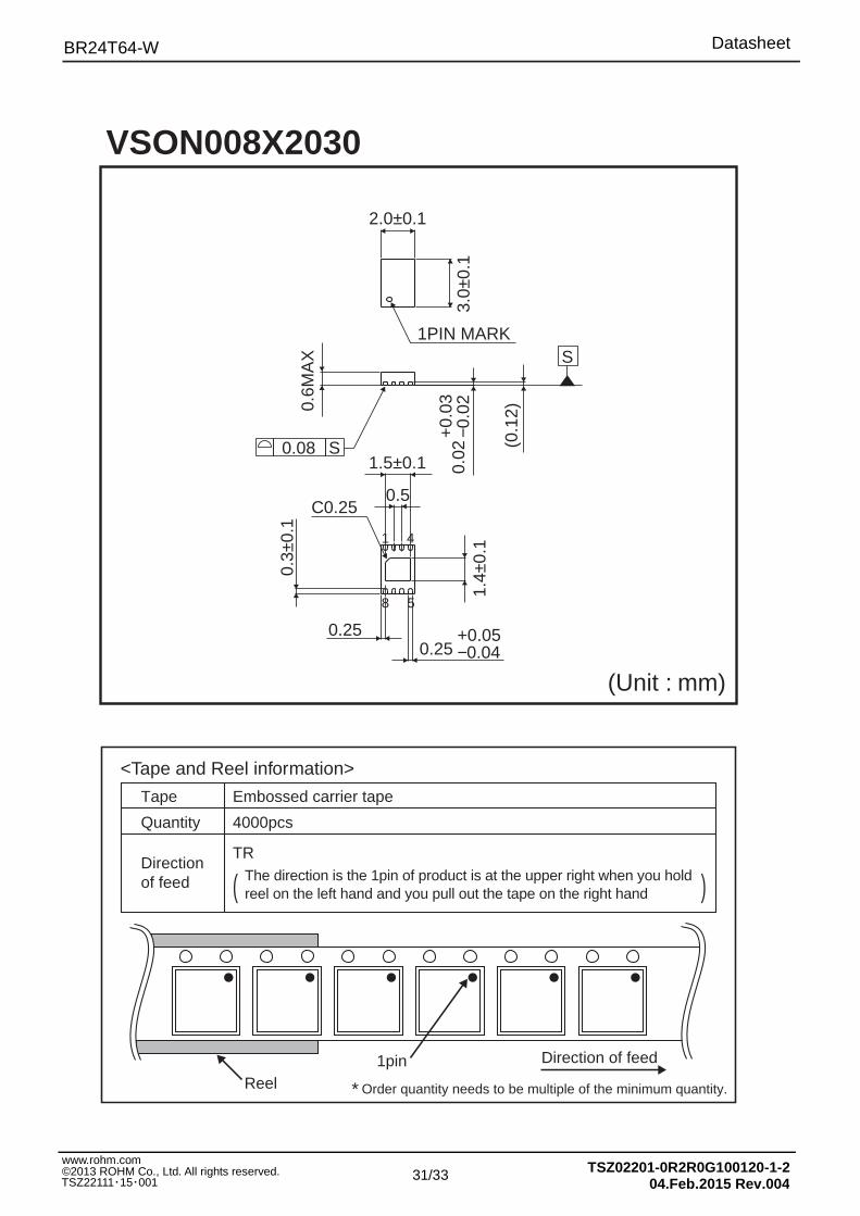
VSON008X2030
5
1
8
4
1.4±
0.1
0.25
1.5±0.1
0.5
0.3±
0.1
0.25+0.05−0.04
C0.25
0.6M
AX
(0.1
2)
0.02
+0.
03−0
.02
3.0±
0.1
2.0±0.1
1PIN MARK
0.08 S
S

Datasheet
32/33
BR24T64-W
TSZ02201-0R2R0G100120-1-2 04.Feb.2015 Rev.004
©2013 ROHM Co., Ltd. All rights reserved. TSZ22111・15・001
www.rohm.com
Marking Diagrams (TOP VIEW)
DIP-T8 (TOP VIEW)
BR24T64
Part Number Marking
LOT Number
SOP8 (TOP VIEW)
Part Number Marking
LOT Number
1PIN MARK
SOP-J8 (TOP VIEW)
Part Number Marking
LOT Number
1PIN MARK
TSSOP-B8 (TOP VIEW)
Part Number Marking
LOT Number
1PIN MARK
TSSOP-B8J (TOP VIEW)
Part Number Marking
LOT Number
1PIN MARK
SSOP-B8 (TOP VIEW)
Part Number Marking
LOT Number
1PIN MARK
VSON008X2030 (TOP VIEW)
Part Number Marking
LOT Number
1PIN MARK
T 6 4
T 6 4 T 6 4
T 6
4 T 6 4
MSOP8 (TOP VIEW)
Part Number Marking
LOT Number
1PIN MARK
T 6 4 T 6 4
Datasheet
33/33
BR24T64-W
TSZ02201-0R2R0G100120-1-2 04.Feb.2015 Rev.004
©2013 ROHM Co., Ltd. All rights reserved. TSZ22111・15・001
www.rohm.com
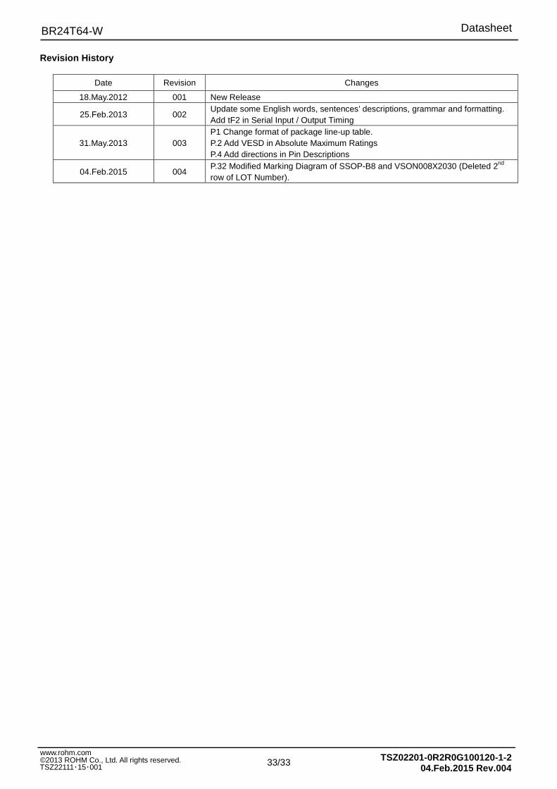
Revision History
Date Revision Changes
18.May.2012 001 New Release
25.Feb.2013 002 Update some English words, sentences’ descriptions, grammar and formatting. Add tF2 in Serial Input / Output Timing
31.May.2013 003 P1 Change format of package line-up table. P.2 Add VESD in Absolute Maximum Ratings P.4 Add directions in Pin Descriptions
04.Feb.2015 004 P.32 Modified Marking Diagram of SSOP-B8 and VSON008X2030 (Deleted 2nd row of LOT Number).

DatasheetDatasheet
Notice-GE Rev.004© 2013 ROHM Co., Ltd. All rights reserved.
Notice Precaution on using ROHM Products
1. Our Products are designed and manufactured for application in ordinary electronic equipments (such as AV equipment, OA equipment, telecommunication equipment, home electronic appliances, amusement equipment, etc.). If you intend to use our Products in devices requiring extremely high reliability (such as medical equipment (Note 1), transport equipment, traffic equipment, aircraft/spacecraft, nuclear power controllers, fuel controllers, car equipment including car accessories, safety devices, etc.) and whose malfunction or failure may cause loss of human life, bodily injury or serious damage to property (“Specific Applications”), please consult with the ROHM sales representative in advance. Unless otherwise agreed in writing by ROHM in advance, ROHM shall not be in any way responsible or liable for any damages, expenses or losses incurred by you or third parties arising from the use of any ROHM’s Products for Specific Applications.
(Note1) Medical Equipment Classification of the Specific Applications JAPAN USA EU CHINA
CLASSⅢ CLASSⅢ
CLASSⅡb CLASSⅢ
CLASSⅣ CLASSⅢ
2. ROHM designs and manufactures its Products subject to strict quality control system. However, semiconductor
products can fail or malfunction at a certain rate. Please be sure to implement, at your own responsibilities, adequate safety measures including but not limited to fail-safe design against the physical injury, damage to any property, which a failure or malfunction of our Products may cause. The following are examples of safety measures:
[a] Installation of protection circuits or other protective devices to improve system safety [b] Installation of redundant circuits to reduce the impact of single or multiple circuit failure
3. Our Products are designed and manufactured for use under standard conditions and not under any special or extraordinary environments or conditions, as exemplified below. Accordingly, ROHM shall not be in any way responsible or liable for any damages, expenses or losses arising from the use of any ROHM’s Products under any special or extraordinary environments or conditions. If you intend to use our Products under any special or extraordinary environments or conditions (as exemplified below), your independent verification and confirmation of product performance, reliability, etc, prior to use, must be necessary:
[a] Use of our Products in any types of liquid, including water, oils, chemicals, and organic solvents [b] Use of our Products outdoors or in places where the Products are exposed to direct sunlight or dust [c] Use of our Products in places where the Products are exposed to sea wind or corrosive gases, including Cl2,
H2S, NH3, SO2, and NO2
[d] Use of our Products in places where the Products are exposed to static electricity or electromagnetic waves [e] Use of our Products in proximity to heat-producing components, plastic cords, or other flammable items [f] Sealing or coating our Products with resin or other coating materials [g] Use of our Products without cleaning residue of flux (even if you use no-clean type fluxes, cleaning residue of
flux is recommended); or Washing our Products by using water or water-soluble cleaning agents for cleaning residue after soldering
[h] Use of the Products in places subject to dew condensation
4. The Products are not subject to radiation-proof design. 5. Please verify and confirm characteristics of the final or mounted products in using the Products. 6. In particular, if a transient load (a large amount of load applied in a short period of time, such as pulse. is applied,
confirmation of performance characteristics after on-board mounting is strongly recommended. Avoid applying power exceeding normal rated power; exceeding the power rating under steady-state loading condition may negatively affect product performance and reliability.
7. De-rate Power Dissipation (Pd) depending on Ambient temperature (Ta). When used in sealed area, confirm the actual
ambient temperature. 8. Confirm that operation temperature is within the specified range described in the product specification. 9. ROHM shall not be in any way responsible or liable for failure induced under deviant condition from what is defined in
this document.
Precaution for Mounting / Circuit board design 1. When a highly active halogenous (chlorine, bromine, etc.) flux is used, the residue of flux may negatively affect product
performance and reliability.
2. In principle, the reflow soldering method must be used on a surface-mount products, the flow soldering method must be used on a through hole mount products. If the flow soldering method is preferred on a surface-mount products, please consult with the ROHM representative in advance.
For details, please refer to ROHM Mounting specification

DatasheetDatasheet
Notice-GE Rev.004© 2013 ROHM Co., Ltd. All rights reserved.
Precautions Regarding Application Examples and External Circuits 1. If change is made to the constant of an external circuit, please allow a sufficient margin considering variations of the
characteristics of the Products and external components, including transient characteristics, as well as static characteristics.
2. You agree that application notes, reference designs, and associated data and information contained in this document
are presented only as guidance for Products use. Therefore, in case you use such information, you are solely responsible for it and you must exercise your own independent verification and judgment in the use of such information contained in this document. ROHM shall not be in any way responsible or liable for any damages, expenses or losses incurred by you or third parties arising from the use of such information.
Precaution for Electrostatic
This Product is electrostatic sensitive product, which may be damaged due to electrostatic discharge. Please take proper caution in your manufacturing process and storage so that voltage exceeding the Products maximum rating will not be applied to Products. Please take special care under dry condition (e.g. Grounding of human body / equipment / solder iron, isolation from charged objects, setting of Ionizer, friction prevention and temperature / humidity control).
Precaution for Storage / Transportation 1. Product performance and soldered connections may deteriorate if the Products are stored in the places where:
[a] the Products are exposed to sea winds or corrosive gases, including Cl2, H2S, NH3, SO2, and NO2 [b] the temperature or humidity exceeds those recommended by ROHM [c] the Products are exposed to direct sunshine or condensation [d] the Products are exposed to high Electrostatic
2. Even under ROHM recommended storage condition, solderability of products out of recommended storage time period may be degraded. It is strongly recommended to confirm solderability before using Products of which storage time is exceeding the recommended storage time period.
3. Store / transport cartons in the correct direction, which is indicated on a carton with a symbol. Otherwise bent leads
may occur due to excessive stress applied when dropping of a carton. 4. Use Products within the specified time after opening a humidity barrier bag. Baking is required before using Products of
which storage time is exceeding the recommended storage time period.
Precaution for Product Label QR code printed on ROHM Products label is for ROHM’s internal use only.
Precaution for Disposition When disposing Products please dispose them properly using an authorized industry waste company.
Precaution for Foreign Exchange and Foreign Trade act Since our Products might fall under controlled goods prescribed by the applicable foreign exchange and foreign trade act, please consult with ROHM representative in case of export.
Precaution Regarding Intellectual Property Rights 1. All information and data including but not limited to application example contained in this document is for reference
only. ROHM does not warrant that foregoing information or data will not infringe any intellectual property rights or any other rights of any third party regarding such information or data. ROHM shall not be in any way responsible or liable for infringement of any intellectual property rights or other damages arising from use of such information or data.:
2. No license, expressly or implied, is granted hereby under any intellectual property rights or other rights of ROHM or any
third parties with respect to the information contained in this document.
Other Precaution 1. This document may not be reprinted or reproduced, in whole or in part, without prior written consent of ROHM. 2. The Products may not be disassembled, converted, modified, reproduced or otherwise changed without prior written
consent of ROHM. 3. In no event shall you use in any way whatsoever the Products and the related technical information contained in the
Products or this document for any military purposes, including but not limited to, the development of mass-destruction weapons.
4. The proper names of companies or products described in this document are trademarks or registered trademarks of
ROHM, its affiliated companies or third parties.
DatasheetDatasheet
Notice – WE Rev.001© 2015 ROHM Co., Ltd. All rights reserved.
General Precaution 1. Before you use our Pro ducts, you are requested to care fully read this document and fully understand its contents.
ROHM shall n ot be in an y way responsible or liabl e for fa ilure, malfunction or acci dent arising from the use of a ny ROHM’s Products against warning, caution or note contained in this document.
2. All information contained in this docume nt is current as of the issuing date and subj ect to change without any prior
notice. Before purchasing or using ROHM’s Products, please confirm the la test information with a ROHM sale s representative.
3. The information contained in this doc ument is provi ded on an “as is” basis and ROHM does not warrant that all
information contained in this document is accurate an d/or error-free. ROHM shall not be in an y way responsible or liable for any damages, expenses or losses incurred by you or third parties resulting from inaccuracy or errors of or concerning such information.
Related Documents