Hyperstone F2-16X 32-Bit Flash Memory Controller Specification

Welcome message from author
This document is posted to help you gain knowledge. Please leave a comment to let me know what you think about it! Share it to your friends and learn new things together.
Transcript

Hyperstone F2-16X
32-Bit Flash Memory Controller Specification
Specifications and information in this document are subject to change without notice and do not represent a commitment on the part of Hyperstone AG. Hyperstone AG reserves the right to make changes to improve functioning. Although the information in this document has been carefully reviewed, Hyperstone AG does not assume any liability arising out of the use of the product or circuit described herein.
Hyperstone AG does not authorize the use of the Hyperstone microprocessor in life support applications wherein a failure or malfunction of the microprocessor may directly threaten life or cause injury. The user of the Hyperstone microprocessor in life support applications assumes all risks of such use and indemnifies Hyperstone AG against all damages.
No part of this manual may be reproduced or transmitted in any form or by any means, electronic or mechanical, including photocopying and recording, for any purpose without the permission of Hyperstone AG.
Hyperstone is a registered trademark of Hyperstone AG.
For further information please contact:
Hyperstone AG Am Seerhein 8 D-78467 Konstanz Germany Phone +49 – 7531 - 98030 Fax +49 – 7531 - 51725 E-Mail [email protected]
URL: http://www.hyperstone.com
Copyright 1990 – 2006 Hyperstone AG
Revision 03/06 FU5

TABLE OF CONTENTS 1
Table of Contents Revision History ...........................................................................................................2 1. Features ...............................................................................................................3
1.1. Host interface...........................................................................................3 1.2. Flash Memory Interface ..........................................................................3 1.3. Controller Core........................................................................................3
2. General Description.............................................................................................4 3. Pin Configuration ................................................................................................6
3.1. hyperstone F2-16XN, F2-L16XN, F2-IL16XN, 128-Pin Package .........6 3.2. hyperstone F2-16XT and F2-L16XT, 100-Pin Package..........................9 3.3. hyperstone F2-L16XB, 100-Pin Package ..............................................12 3.4. Package Dimensions TQFP...................................................................15 3.5. Package Dimensions TFBGA................................................................17 3.6. Bus Signals ............................................................................................19
4. Functional Description ......................................................................................24 4.1. Block Diagram.......................................................................................24 4.2. System Memory Map ............................................................................24 4.3. Flash Memory Interface ........................................................................25 4.4. ECC Unit ...............................................................................................25 4.5. SmartMedia Unit ...................................................................................26 4.6. Reset and ROM boot .............................................................................27 4.7. PCMCIA Interface.................................................................................27 4.8. Register and Sector Buffer Access Modes ............................................37 4.9. Hyperstone Sector Buffer Access..........................................................40 4.10. Internal ROM.........................................................................................41
5. Electrical Specifications....................................................................................42 5.1. DC Characteristics.................................................................................42 5.2. AC Characteristics.................................................................................43

2 FEATURES
Revision History Revision Change History Date
08/02 Initial release Aug 30, 2002
03/05 Product names for lead free package 128 pin package correction (TQFP, 1.0mm) Hitachi flash references removed
Mar 08, 2005
12/05 Added 100 pin TFBGA package Dec 08, 2005
03/06 Added extended temperature range version Mar 10, 2006

TABLE OF CONTENTS 3
1. Features
1.1. Host interface PCMCIA 2.1 and PC Card ATA standard compatible
Memory mapped or I/O operation
Fast ATA host-to-buffer transfer rates supporting PIO 4 in True-IDE mode
Automatic sensing of PCMCIA or True-IDE host interface mode
Dual integrated 512 Byte PCMCIA Sector Buffers and 256 Byte PCMCIA Attribute Memory
PCMCIA Configuration Option Register, Card Configuration and Status Register and Pin Replacement Register support
1.2. Flash Memory Interface Supports all control signal for serial type flash memory connection
Supports direct connection of up to 16 (F2-16XN) or 10 (F2-16XT) flash memory chips
Supports 32, 64, 128, 256, 512Mbit, 1, 2, 4 Gbit Samsung (NAND) type flash memories
Supports 256 Mbit and 1Gbit AG-AND type flash memories
Flash memory power down logic and flash memory write protect control
Firmware storage in flash memory
Firmware is loaded into internal memory by the boot ROM
Error Correcting Code capable of correcting 6 bytes in a 512 byte sector
On-chip voltage regulator for 3.3V flash memory power supply
On-chip voltage regulator for 2.5V processor core power supply
1.3. Controller Core High performance microprocessor core based on the Hyperstone architecture
Clock frequency 20MHz or 40MHz using R-C oscillator
8 Kbyte Internal Boot ROM
16 Kbyte internal RAM
Automatic power-down mode during wait periods for host data or flash memory operation completion
Automatic sleep mode during host inactivity periods, Icc < 200 µA
128 pin TQFP (14×14×1.0 mm, F2-16XN), 100 pin TQFP (14×14×1.0 mm, F2-16XT) ), 100 pin TFBGA (10×10×1.2 mm, F2-L16XB)
Lead free versions are F2-L16XN, F2-IL16XN, F2-L16XT and F2-L16XB.
0.25 µm CMOS technology
Supply voltage 5.0V ±10% or 3.3V ±10%
4 GENERAL DESCRIPTION
2. General Description The Hyperstone F2-16XN and F2-16XT flash memory controllers are among the most powerful single-chip controllers on the market for designing ATA based Flash Memory PC Cards / CompactFlash Cards. The required external component count is reduced to a bare minimum of few passive components enabling the design of very low-cost but high-performance ATA flash memory cards / CompactFlash Cards.
The Hyperstone F2-16X flash memory controller can operate with NAND or AG-AND type flash memory devices. It operates with 5.0V and 3.3V and enables automatic voltage detection for the cards. A highly sophisticated Error Correction Code and a wear-leveling algorithm are also implemented. A complete set of development tools is available which enables you to design ATA Flash Memory Cards / CompactFlash Cards with a very competitive cost/performance ratio.
The main features of Hyperstone F2-16X flash memory controller are:
Inexpensive single-chip controller for ATA flash memory cards / CompactFlash cards
Full support for NAND and AG-AND type flash memories
Built-in 3.3V voltage regulator for flash memory supply
Built-in 2.5V voltage regulator for processor core supply
Built-in PC card / CompactFlash Interface
Data transfer rate to flash memories: up to 20 MBytes/s
Supports True-IDE mode
On-chip ECC unit
Sophisticated software for wear leveling
Automatic power-down mode and sleep mode
Small 128-pin TQFP package (F2-16XN)
Available in a 100-pin TQFP package (F2-16XT) or a 100-pin TFBGA package (F2-L16XB) for low-cost CompactFlash Card applications supporting up to 10 flash memory chips
Lead free versions are F2-L16XN, F2-L16XT and F2-L16XB
Industrial temperature range available for the 128 pin package (F2-IL16XN)
Comprehensive equipment available for development and test of hardware and firmware
The Hyperstone F2-16X single-chip controller for ATA Flash Memory Cards / CompactFlash Cards is based on the Hyperstone E1-32X microprocessor core providing a modern 32-bit RISC architecture. The controller’s flash memory interface allows the direct connection of up to 16 flash memory chips (10 chips for the F2-16XT) and supports either Samsung (NAND) type or AG-AND type flash memories (32 Mbit to 4 Gbit). Next-generation flash memories will be supported as well. Through the sophisticated memory interface of the Hyperstone F2-16X, your flash memory card will achieve a superior performance with a data transfer rate to flash memories of up to 20 MBytes/s. An on-chip ECC unit generates the required code bytes for error detection and correction of up to six bytes per 512 Byte data sector. Code byte generation during write operations as well as
GENERAL DESCRIPTION 5
error detection during read operation is implemented on the fly without any speed penalties.
The controller is equipped with 16 KByte internal memory that is used for storage of code and data. The internal memory can also be used as an intermediate memory for storing data blocks during a wear-leveling procedure.
The Hyperstone F2-16X controller works at power supply voltages of 5.0V as well as 3.3V. It provides a built-in voltage regulator of 3.3V to supply flash memories with the required voltage even when the interface from the host offers just a voltage of 5.0V.
An 8 KByte internal boot ROM includes basic routines for accessing the flash memories and for loading the main code into the internal memory of the Hyperstone F2-16X. This boot concept offers a high degree of flexibility while keeping the component count small.
The PC Card / CompactFlash interface provides all required signals and is fully compliant with the PC Card standard Rel. 2.1. The PC Card controller part of the Hyperstone F2-16X includes 256 Byte attribute memory, PCMCIA configuration and status registers, two 512 Byte sector buffers and the complete ATA register set. Optionally, the controller can be operated in True-IDE mode.
A comprehensive tool kit is also available for developing and testing ATA Flash Memory Cards / CompactFlash Cards based on Hyperstone F2-16X. This includes a HW/SW test environment, pre-format HW/SW, Firmware for ECC and wear leveling.
6 PIN CONFIGURATION
3. Pin Configuration
3.1. hyperstone F2-16XN, F2-L16XN, F2-IL16XN, 128-Pin Package
3.1.1. Pin Configuration - View from Top Side
hyFlashF2-16XN
979899100101102103104105106107108109110111112113114115116117118119120121122123124125126127128
D0A8
OE#VCC_F
A7A6A5
GND_FA4A3A2
IOWR#IORD#PD10
PIOIS16#A0A1
PD9PD2PD8
VCC_PPD1
PSTSCHG#INT4PD0
PSPKR#GND_P
PA0PREG#
GND_F
90 89 88 87 86 85 84 83 82 81 80 79 78 77 76 75 74 73 72 71 70 69 68 67 66 65919293949596
D11
D6
WE2
#FO
E#
GN
D_F
XTA
LIX
TALC
XTA
LRD
2D
5W
E3#
FWE#
D3
D4
FRD
YV
CC
_CV
CC
_CG
ND
_CG
ND
_CFR
ES#
FHO
E#V
CC
_FW
E#C
S3#
CS1
#
D12
D10
D13
D9
D14
1 2 3 4 6 7 8 9 10 11 125 13 14 15 16 17 18 19 20 21 22 23 24 25 26 27 28 29 30 31 32
PA2
PWA
IT#
A19
PA3
PR
ESET
#P
A4
PC
SEL#
PA6A1
8
VCC
_PG
ND
_P PA7
PWE
#P
A8VC
C_C
GN
D_C
GN
D_C
PIO
WR
#P
A9PI
OR
D#
A16
A15
POE
#PA
10PC
E2#
PCE1
#PD
15A17
PA5
60595857565554535251504948474645444342414039383736353433
61626364
GND_F
A11A10
CADJ
VCC_RFADJFOUTFOUTPD3BUSRQ#A14PD11PD4PD12
PD5PD13PD6PD14GND_P
VCC_RGND_RVCC_R
COUTA9
RESET#D15A13A12
PIN
PAC
K#
PD7
GND_P
GND_F
VCC_F
VCC_P
PA1
D7
D1
D8
PIR
EQ#
Figure 1: Hyperstone F2-16XN, F2-L16XN, F2-IL16XN, 128 Pin TQFP Package

PIN CONFIGURATION 7
3.1.2. Pin Cross Reference by Pin Name
Signal Location Signal Location Signal Location Signal Location
A0 ................... 114 D15................... 61 IORD# ............ 111 PD9 ................ 116 A1 ................... 115 D2..................... 87 IOWR#............ 110 PINPACK# ......... 1 A10 ................... 56 D3..................... 84 OE# ................ 100 PIOIS16#........ 113 A11 ................... 57 D4..................... 83 PA0................. 126 PIORD#............ 24 A12 ................... 59 D5..................... 86 PA1................. 128 PIOWR# ........... 22 A13 ................... 60 D6..................... 95 PA10................. 28 PIREQ# ............ 15 A14 ................... 43 D7..................... 97 PA2..................... 2 POE#................ 27 A15 ................... 26 D8..................... 65 PA3..................... 7 PREG# ........... 127 A16 ................... 25 D9..................... 67 PA4..................... 9 PRESET#........... 8 A17 ..................... 6 FADJ................. 48 PA5................... 10 PSPKR# ......... 124 A18 ..................... 5 FHOE# ............. 76 PA6................... 12 PSTSCHG#.... 121 A19 ..................... 4 FOE# ................ 93 PA7................... 16 PWE# ............... 17 A2 ................... 109 FOUT................ 46 PA8................... 18 PWAIT#.............. 3 A3 ................... 108 FOUT................ 47 PA9................... 23 RESET# ........... 62 A4 ................... 107 FRDY................ 82 PCE1# .............. 30 VCC_C ............. 19 A5 ................... 104 FRES#.............. 77 PCE2# .............. 29 VCC_C ............. 80 A6 ................... 103 FEW#................ 92 PCSEL#............ 11 VCC_C ............. 81 A7 ................... 102 GND_C............. 20 PD0 ................ 123 VCC_F.............. 58 A8 ..................... 99 GND_C............. 21 PD1 ................ 120 VCC_F.............. 75 A9 ..................... 55 GND_C............. 78 PD10 .............. 112 VCC_F............ 101 BUSRQ#........... 44 GND_C............. 79 PD11 ................ 42 VCC_P ............. 13 CADJ ................ 53 GND_F ............. 63 PD12 ................ 40 VCC_P ............. 39 COUT ............... 54 GND_F ............. 64 PD13 ................ 37 VCC_P ........... 119 CS1#................. 72 GND_F ............. 91 PD14 ................ 35 VCC_R ............. 49 CS3#................. 73 GND_F ........... 105 PD15 ................ 31 VCC_R ............. 50 D0 ..................... 98 GND_F ........... 106 PD2 ................ 117 VCC_R ............. 52 D1 ..................... 96 GND_P ............. 14 PD3 .................. 45 WE#.................. 74 D10 ................... 69 GND_P ............. 33 PD4 .................. 41 WE2#................ 94 D11 ................... 71 GND_P ............. 34 PD5 .................. 38 WE3#................ 85 D12 ................... 70 GND_P ........... 125 PD6 .................. 36 XTALC.............. 89 D13 ................... 68 GND_R............. 51 PD7 .................. 32 XTALI ............... 90 D14 ................... 66 INT4................ 122 PD8 ................ 118 XTALR.............. 88

8 PIN CONFIGURATION
3.1.3. Pin Cross Reference by Location
Location Signal Location Signal Location Signal Location Signal
1.......... PINPACK# 33..............GND_P 65......................D8 97......................D7 2..................... PA2 34..............GND_P 66....................D14 98......................D0 3.................PWIT# 35................. PD14 67......................D9 99......................A8 4......................A19 36................... PD6 68....................D13 100 ................ OE# 5......................A18 37................. PD13 69....................D10 101 ........... VCC_F 6......................A17 38................... PD5 70....................D12 102 ...................A7 7..................... PA3 39..............VCC_P 71....................D11 103 ...................A6 8............PRESET# 40................. PD12 72................. CS1# 104 ...................A5 9..................... PA4 41................... PD4 73................. CS3# 105 ...........GND_F 10................... PA5 42................. PD11 74.................. WE# 106 ...........GND_F 11............ PCSEL# 43....................A14 75.............. VCC_F 107 ...................A4 12................... PA6 44........... BUSRQ# 76.............. FHOE# 108 ...................A3 13..............VCC_P 45................... PD3 77...............FRES# 109 ...................A2 14..............GND_P 46................ FOUT 78............. GND_C 110 ........... IOWR# 15.............PIREQ# 47................ FOUT 79............. GND_C 111 ............ IORD# 16................... PA7 48................. FADJ 80..............VCC_C 112 .............. PD10 17................PWE# 49..............VCC_R 81..............VCC_C 113 ........PIOIS16# 18................... PA8 50..............VCC_R 82................ FRDY 114 ...................A0 19..............VCC_C 51............. GND_R 83......................D4 115 ...................A1 20............. GND_C 52..............VCC_R 84......................D3 116 ................ PD9 21............. GND_C 53.................CADJ 85................ WE3# 117 ................ PD2 22............PIOWR# 54................COUT 86......................D5 118 ................ PD8 23................... PA9 55......................A9 87......................D2 119 ........... VCC_P 24.............PIORD# 56....................A10 88...............XTALR 120 ................ PD1 25....................A16 57....................A11 89...............XTALC 121 ....PSTSCHG# 26....................A15 58.............. VCC_F 90................ XTALI 122 ............... INT4 27................ POE# 59....................A12 91..............GND_F 123 ................ PD0 28................. PA10 60....................A13 92................ FWE# 124 .........PSPKR# 29...............PCE2# 61................... D15 93.................FOE# 125 ...........GND_P 30...............PCE1# 62............RESET# 94................ WE2# 126 ................ PA0 31.................PD15 63..............GND_F 95......................D6 127 ...........PREG# 32...................PD7 64..............GND_F 96......................D1 128 ................ PA1
PIN CONFIGURATION 9
3.2. hyperstone F2-16XT and F2-L16XT, 100-Pin Package
3.2.1. Pin Configuration - View from Top Side
21 3 4 5 6 7 8 9 10 11 12 13 14 15 16 17 18 19 20 21 22 23 24 25
75 74 73 72 71 70 69 68 67 66 65 63 62 61 60 59 58 57 56 55 54 53
90919293949596979899100
64
373635343332
3839
PD8PD2PD9
PIOIS16#PD10
A2A3A4
GND_FA5A6A7
VCC_FA8D0D7
PD4PD11PD3FOUTFADJVCC_RGND_RVCC_RCADJCOUTA9A10A11A12A13D15RESET#GND_F
PIN
PAC
K#
PA2
PW
AIT#
PA3
PRES
ET#
PA4
PA5
PCSE
L#PA
6G
ND
_PP
IRE
Q#
PA7
PW
E# PA8
VCC
_CG
ND
_CP
IOW
R#
D6
FOE#
FWE
#G
ND
_FXT
ALI
XTA
LCXT
ALR
D2
D5
D3
D4
FRD
YVC
C_C
GN
D_C
FRES
#FH
OE
#VC
C_F
D10
D13
D9
D14
D8
GND_PPD14PD6PD13PD5VCC_PPD12
PA9
PIO
RD
#PO
E#
PC
E2#
PC
E1#
PD15
PD
7
PA1PREG#
PA0GND_P
PSPKR#PD0
PSTSCHG#PD1
VCC_P
50
D1
hyFlashF2-16XT
313029282726
77
7980818283848586878889
76
78 4847
49
46454443424140
52 51
D11
D12
PA10
Figure 2: Hyperstone F2-16XT and F2-L16XT, 100 Pin TQFP Package
10 PIN CONFIGURATION
3.2.2. Pin Cross Reference by Pin Name
Signal Location Signal Location Signal Location Signal Location
A10 ................... 44 D5 ..................... 66 PA3..................... 4 PD9 .................. 89 A11 ................... 45 D6 ..................... 74 PA4..................... 6 PINPACK#.......... 1 A12 ................... 46 D7 ..................... 76 PA5..................... 7 PIOIS16#.......... 88 A13 ................... 47 D8 ..................... 51 PA6..................... 9 PIORD# ............ 19 A2 ..................... 86 D9 ..................... 53 PA7................... 12 PIOWR# ........... 17 A3 ..................... 85 FADJ................. 37 PA8................... 14 PIREQ# ............ 11 A4 ..................... 84 FHOE#.............. 59 PA9................... 18 POE#................ 20 A5 ..................... 82 FOE# ................ 73 PCE1# .............. 23 PREG# ............. 99 A6 ..................... 81 FOUT................ 36 PCE2# .............. 22 PRESET# ........... 5 A7 ..................... 80 FRDY................ 63 PCSEL#.............. 8 PSPKR# ........... 96 A8 ..................... 78 FRES# .............. 60 PD0................... 95 PSTSCHG#...... 94 A9 ..................... 43 FWE#................ 72 PD1................... 93 PWAIT# .............. 3 CADJ ................ 41 GND_C............. 16 PD10................. 87 PWE# ............... 13 COUT................ 42 GND_C............. 61 PD11................. 34 RESET# ........... 49 D0 ..................... 77 GND_F ............. 50 PD12................. 32 VCC_C ............. 15 D1 ..................... 75 GND_F ............. 71 PD13................. 29 VCC_C ............. 62 D10 ................... 55 GND_F ............. 83 PD14................. 27 VCC_F.............. 58 D11 ................... 57 GND_P ............. 10 PD15................. 24 VCC_F.............. 79 D12 ................... 56 GND_P ............. 26 PD2................... 90 VCC_P ............. 31 D13 ................... 54 GND_P ............. 97 PD3................... 35 VCC_P ............. 92 D14 ................... 52 GND_R............. 39 PD4................... 33 VCC_R ............. 38 D15 ................... 48 PA0................... 98 PD5................... 30 VCC_R ............. 40 D2 ..................... 67 PA1................. 100 PD6................... 28 XTALC.............. 69 D3 ..................... 65 PA10................. 21 PD7................... 25 XTALI ............... 70 D4 ..................... 64 PA2..................... 2 PD8................... 91 XTALR.............. 68

PIN CONFIGURATION 11
3.2.3. Pin Cross Reference by Location
Location Signal Location Signal Location Signal Location Signal
1.......... PINPACK# 26..............GND_P 51 .....................D8 76 .....................D7 2..................... PA2 27................. PD14 52 ...................D14 77 .....................D0 3...............PWAIT# 28................... PD6 53 .....................D9 78 .....................A8 4..................... PA3 29................. PD13 54 ...................D13 79 ..............VCC_F 5............PRESET# 30................... PD5 55 ...................D10 80 .....................A7 6..................... PA4 31.............. VCC_P 56 ...................D12 81 .....................A6 7..................... PA5 32................. PD12 57 ...................D11 82 .....................A5 8.............. PCSEL# 33................... PD4 58 ............. VCC_F 83 ............. GND_F 9..................... PA6 34................. PD11 59 ............. FHOE# 84 .....................A4 10..............GND_P 35................... PD3 60 ..............FRES# 85 .....................A3 11.............PIREQ# 36................ FOUT 61 .............GND_C 86 .....................A2 12................... PA7 37................. FADJ 62 .............VCC_C 87 ................ PD10 13................PWE# 38..............VCC_R 63 ............... FRDY 88 ..........PIOIS16# 14................... PA8 39..............GND_R 64 .....................D4 89 .................. PD9 15..............VCC_C 40..............VCC_R 65 .....................D3 90 .................. PD2 16............. GND_C 41.................CADJ 66 .....................D5 91 .................. PD8 17............PIOWR# 42................COUT 67 .....................D2 92 ............. VCC_P 18................... PA9 43......................A9 68 ..............XTALR 93 .................. PD1 19.............PIORD# 44....................A10 69 ..............XTALC 94 ......PSTSCHG# 20................ POE# 45....................A11 70 ............... XTALI 95 .................. PD0 21................. PA10 46....................A12 71 .............GND_F 96 ........... PSPKR# 22...............PCE2# 47....................A13 72 ............... FWE# 97 .............GND_P 23...............PCE1# 48....................D15 73 ................FOE# 98 ...................PA0 24................. PD15 49............ RESET# 74 .....................D6 99 ............. PREG# 25................... PD7 50..............GND_F 75 .....................D1 100 .................PA1

12 PIN CONFIGURATION
3.3. hyperstone F2-L16XB, 100-Pin Package
3.3.1. Pin Configuration - View from Top Side
1 2 3 4 5 6 7 8 9 10
FOE# D4FWE# D12XTALC FHOE#D2 RESET#D9 A13
D0 FRDYD6 D10XTALI FRES#XTALR D15D14 A12
A7 D3A8 D13D1 D11D5 A11D8 A10
A5 GND_CA6 GND_FD7 VCC_FGND_F A9COUT CADJ
A2 A3
PIOIS16# PD9
PD2 PSTS PD8 PD12
PD1 PRESET#PD0 PIOWR#PSPKR# PA7PA3 PD14POE# PD6
PA0 PA6PA1 PA9PA2 PWE#PA5 PD15PCE2# PD7
PREG# PCSEL#PINP
PA8PWAIT# PIREQ#PA4 PA10PIORD# PCE1#
VCC_C VCC_RA4 VCC_FGND_F FADJGND_R PD11
VCC_C VCC_RPD10 GND_CVCC_P PD3FOUT PD4
GND_P GND_PGND_PVCC_P PD5PD13
ACK#
1 2 3 4 5 6 7 8 9 10
A
B
C
D
E
F
G
H
J
K
A
B
C
D
E
F
G
H
J
K
CHG#
Figure 3: Hyperstone F2-L16XB, 100 Pin TFBGA Package

PIN CONFIGURATION 13
3.3.2. Pin Cross Reference by Pin Name
Signal Location Signal Location Signal Location Signal Location
A10 ................ C10 D5.....................C4 PA3...................H4 PD9 .................. F2 A11 ...................C9 D6.....................B2 PA4...................K4 PINPACK# .......K2 A12 .................B10 D7.....................D3 PA5................... J4 PIOIS16#.......... F1 A13 .................A10 D8.....................C8 PA6................... J5 PIORD#............K8 A2 .....................E1 D9.....................A8 PA7...................H6 PIOWR# ...........H7 A3 .....................E2 FADJ.................E9 PA8...................K7 PIREQ# ............K6 A4 .....................E3 FHOE# .............A6 PA9................... J7 POE#................H8 A5 .....................D1 FOE# ................A1 PCE1# ............K10 PREG# .............K1 A6 .....................D2 FOUT................ F8 PCE2# .............. J8 PRESET#.........H5 A7 .....................C1 FRDY................B5 PCSEL#............K5 PSPKR# ...........H3 A8 .....................C2 FRES#..............B6 PD0 ..................H2 PSTSCHG#......G2 A9 .....................D9 FWE#................A2 PD1 ..................H1 PWAIT#............K3 CADJ ............. D10 GND_C.............D5 PD10 ................ F3 PWE# ................J6 COUT ...............D8 GND_C............. F6 PD11 ..............E10 RESET# ...........A9 D0 .....................B1 GND_F .............D4 PD12 ............. G10 VCC_C .............E5 D1 .....................C3 GND_F .............D7 PD13 ............... G8 VCC_C ............. F5 D10 ...................B7 GND_F .............E4 PD14 ................H9 VCC_F..............D6 D11 ...................C6 GND_P ............ G5 PD15 ................ J9 VCC_F..............E6 D12 ...................A7 GND_P ............ G6 PD2 ................. G1 VCC_P ............. F4 D13 ...................C7 GND_P ............ G7 PD3 .................. F9 VCC_P .............G4 D14 ...................B8 GND_R.............E8 PD4 ................ F10 VCC_R .............E7 D15 ...................B9 PA0................... J1 PD5 ................. G9 VCC_R ............. F7 D2 .....................A4 PA1................... J2 PD6 ................H10 XTALC..............A3 D3 .....................C5 PA10.................K9 PD7 ................ J10 XTALI ...............B3 D4 .....................A5 PA2................... J3 PD8 ................. G3 XTALR..............B4

14 PIN CONFIGURATION
3.3.3. Pin Cross Reference by Location
Location Signal Location Signal Location Signal Location Signal
A1 ................FOE# C6 .................. D11 F1 ......... PIOIS16# H6.................. PA7 A2 ...............FWE# C7 .................. D13 F2 .................. PD9 H7...........PIOWR# A3 ............. XTALC C8 .................... D8 F3 ................ PD10 H8................POE# A4 .................... D2 C9 ...................A11 F4 ............. VCC_P H9................ PD14 A5 .................... D4 C10 .................A10 F5 .............VCC_C H10................ PD6 A6 .............FHOE# D1 .....................A5 F6 ............ GND_C J1................... PA0 A7 .................. D12 D2 .....................A6 F7 .............VCC_R J2................... PA1 A8 .................... D9 D3 .................... D7 F8 ............... FOUT J3................... PA2 A9 ...........RESET# D4 .............GND_F F9 .................. PD3 J4................... PA5 A10 .................A13 D5 ............ GND_C F10 ................ PD4 J5................... PA6 B1 .................... D0 D6 ............. VCC_F G1.................. PD2 J6................PWE# B2 .................... D6 D7 .............GND_F G2......PSTSCHG# J7................... PA9 B3 ...............XTALI D8 ...............COUT G3.................. PD8 J8...............PCE2# B4 ............. XTALR D9 .....................A9 G4............. VCC_P J9................. PD15 B5 ............... FRDY D10 ..............CADJ G5.............GND_P J10................. PD7 B6 ............. FRES# E1 .....................A2 G6.............GND_P K1 .............PREG# B7 .................. D10 E2 .....................A3 G7.............GND_P K2 ....... PINPACK# B8 .................. D14 E3 .....................A4 G8................ PD13 K3 ............PWAIT# B9 .................. D15 E4 .............GND_F G9.................. PD5 K4 .................. PA4 B10 .................A12 E5 .............VCC_C G10.............. PD12 K5 ........... PCSEL# C1 .....................A7 E6 ............. VCC_F H1 .................. PD1 K6 ............PIREQ# C2 .....................A8 E7 .............VCC_R H2 .................. PD0 K7 .................. PA8 C3 .................... D1 E8 ............ GND_R H3 ...........PSPKR# K8 ............PIORD# C4 .................... D5 E9 ................ FADJ H4 .................. PA3 K9 ................ PA10 C5 .................... D3 E10 .............. PD11 H5 .........PRESET# K10 ............PCE1#
PIN CONFIGURATION 15
3.4. Package Dimensions TQFP
b
D
D1
E1
Index
A1
A2
L
Ee
Figure 4: Hyperstone F2-16X Package Outline
Symbol Term Definition
A1 Standoff height Height from ground plane to bottom edge of package
A2 Package height Height of package itself
E, D Overall length & width Length and width including leads
E1, D1 Package length & width Length and width of package
L Lead footprint Length of flat lead section
e Lead pitch Lead pitch
b Lead width Width of a lead

16 PIN CONFIGURATION
Hyperstone F2-16XN, F2-L16XN, 128 Pin TQFP Package
Symbol Dimensions in Millimeters Dimensions in Inches
Min. Nom. Max. Min. Nom. Max
A1 0.05 0.10 0.15 .002 .004 .006
A2 0.95 1.00 1.05 .037 .039 .041
E, D 15.80 16.00 16.20 .622 .630 .638
E1, D1 13.00 14.00 14.10 .547 .551 .555
L 0.45 0.60 0.75 .018 .024 .030
b 0.13 0.18 0.23 .005 .007 .009
e 0.40 .0157
Hyperstone F2-16XT, F2-L16XT, 100 Pin TQFP Package
Symbol Dimensions in Millimeters Dimensions in Inches
Min. Nom. Max. Min. Nom. Max
A1 0.05 0.10 0.15 .002 .004 .006
A2 0.95 1.00 1.05 .037 .039 .041
E, D 15.80 16.00 16.20 .622 .630 .638
E1, D1 13.00 14.00 14.10 .547 .551 .555
L 0.45 0.60 0.75 .018 .024 .030
b 0.17 0.22 0.27 .007 .009 .011
e 0.50 .0197
PIN CONFIGURATION 17
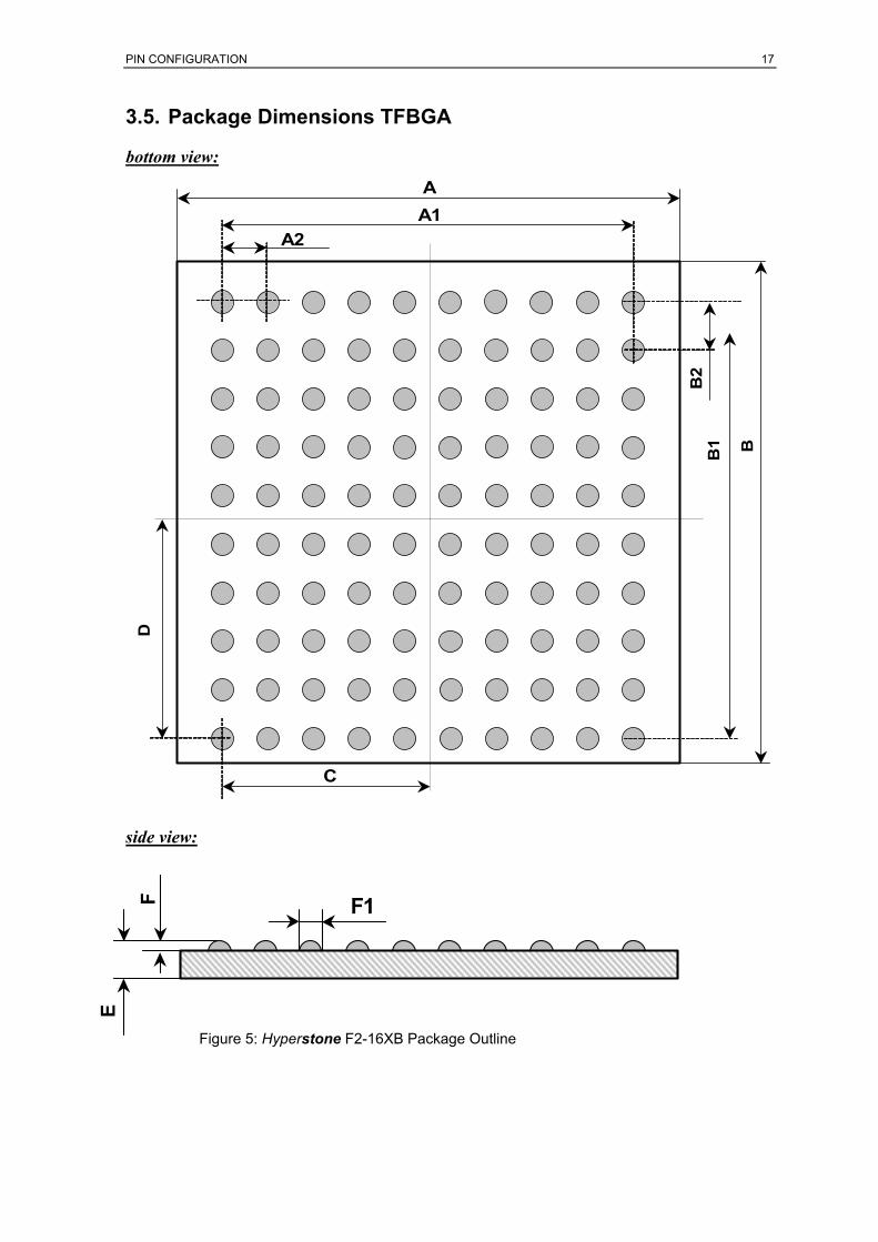
3.5. Package Dimensions TFBGA
bottom view:
AA1
A2
C
D
BB1
B2
side view:
Figure 5: Hyperstone F2-16XB Package Outline
F1F
E
18 PIN CONFIGURATION
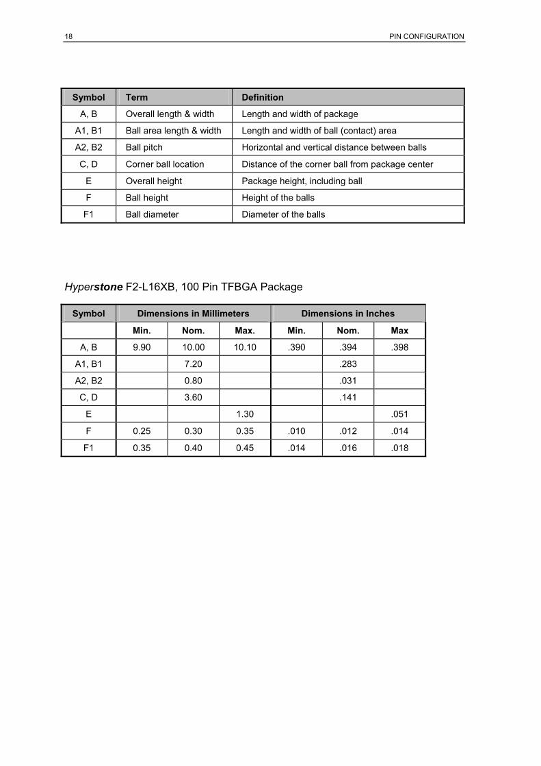
Symbol Term Definition
A, B Overall length & width Length and width of package
A1, B1 Ball area length & width Length and width of ball (contact) area
A2, B2 Ball pitch Horizontal and vertical distance between balls
C, D Corner ball location Distance of the corner ball from package center
E Overall height Package height, including ball
F Ball height Height of the balls
F1 Ball diameter Diameter of the balls
Hyperstone F2-L16XB, 100 Pin TFBGA Package
Symbol Dimensions in Millimeters Dimensions in Inches
Min. Nom. Max. Min. Nom. Max
A, B 9.90 10.00 10.10 .390 .394 .398
A1, B1 7.20 .283
A2, B2 0.80 .031
C, D 3.60 .141
E 1.30 .051
F 0.25 0.30 0.35 .010 .012 .014
F1 0.35 0.40 0.45 .014 .016 .018
PIN CONFIGURATION 19
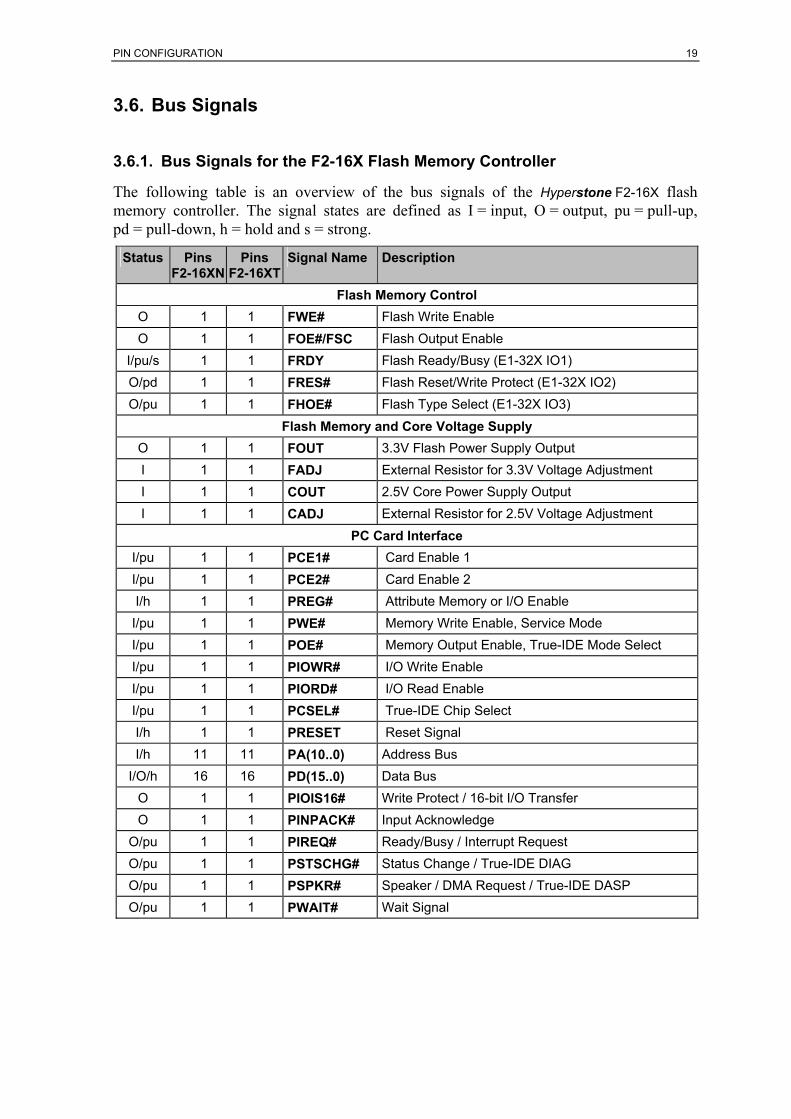
3.6. Bus Signals
3.6.1. Bus Signals for the F2-16X Flash Memory Controller
The following table is an overview of the bus signals of the Hyperstone F2-16X flash memory controller. The signal states are defined as I = input, O = output, pu = pull-up, pd = pull-down, h = hold and s = strong.
Status Pins F2-16XN
Pins F2-16XT
Signal Name Description
Flash Memory Control O 1 1 FWE# Flash Write Enable O 1 1 FOE#/FSC Flash Output Enable
I/pu/s 1 1 FRDY Flash Ready/Busy (E1-32X IO1) O/pd 1 1 FRES# Flash Reset/Write Protect (E1-32X IO2) O/pu 1 1 FHOE# Flash Type Select (E1-32X IO3)
Flash Memory and Core Voltage Supply O 1 1 FOUT 3.3V Flash Power Supply Output I 1 1 FADJ External Resistor for 3.3V Voltage Adjustment I 1 1 COUT 2.5V Core Power Supply Output I 1 1 CADJ External Resistor for 2.5V Voltage Adjustment
PC Card Interface I/pu 1 1 PCE1# Card Enable 1 I/pu 1 1 PCE2# Card Enable 2 I/h 1 1 PREG# Attribute Memory or I/O Enable I/pu 1 1 PWE# Memory Write Enable, Service Mode I/pu 1 1 POE# Memory Output Enable, True-IDE Mode Select I/pu 1 1 PIOWR# I/O Write Enable I/pu 1 1 PIORD# I/O Read Enable I/pu 1 1 PCSEL# True-IDE Chip Select I/h 1 1 PRESET Reset Signal I/h 11 11 PA(10..0) Address Bus
I/O/h 16 16 PD(15..0) Data Bus O 1 1 PIOIS16# Write Protect / 16-bit I/O Transfer O 1 1 PINPACK# Input Acknowledge
O/pu 1 1 PIREQ# Ready/Busy / Interrupt Request O/pu 1 1 PSTSCHG# Status Change / True-IDE DIAG O/pu 1 1 PSPKR# Speaker / DMA Request / True-IDE DASP O/pu 1 1 PWAIT# Wait Signal
20 PIN CONFIGURATION
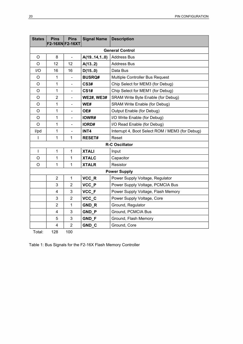
States Pins
F2-16XN Pins
F2-16XT Signal Name Description
General Control O 8 - A(19..14,1..0) Address Bus O 12 12 A(13..2) Address Bus I/O 16 16 D(15..0) Data Bus O 1 - BUSRQ# Multiple Controller Bus Request O 1 - CS3# Chip Select for MEM3 (for Debug) O 1 - CS1# Chip Select for MEM1 (for Debug) O 2 - WE2#, WE3# SRAM Write Byte Enable (for Debug) O 1 - WE# SRAM Write Enable (for Debug) O 1 - OE# Output Enable (for Debug) O 1 - IOWR# I/O Write Enable (for Debug) O 1 - IORD# I/O Read Enable (for Debug)
I/pd 1 - INT4 Interrupt 4, Boot Select ROM / MEM3 (for Debug) I 1 1 RESET# Reset
R-C Oscillator I 1 1 XTALI Input O 1 1 XTALC Capacitor O 1 1 XTALR Resistor
Power Supply 2 1 VCC_R Power Supply Voltage, Regulator 3 2 VCC_P Power Supply Voltage, PCMCIA Bus 4 3 VCC_F Power Supply Voltage, Flash Memory 3 2 VCC_C Power Supply Voltage, Core 2 1 GND_R Ground, Regulator 4 3 GND_P Ground, PCMCIA Bus 5 3 GND_F Ground, Flash Memory 4 2 GND_C Ground, Core
Total: 128 100
Table 1: Bus Signals for the F2-16X Flash Memory Controller

PIN CONFIGURATION 21
3.6.2. Bus Signal Description
The following section describes the bus signals for both the Hyperstone F2-16X controller in detail. In the following signal description, the signal states are defined as I = input, O = output, U = pull-up, D = pull-down.
I XTALI R/C Clock Oscillator Input. This input connects to the other side of the resisors and the capacitor connected to XTALR1, XTALR2 and XTALC. Connect a 22pF capacitor from this pin to ground.
O XTALC R/C Clock Oscillator Capacitor Output. Connect a 22pF capacitor between this pin and XTALI.
O XTALR1 R/C Clock Oscillator Resistor Output. The resistor connected between this pin and XTALI determines the operating clock frequency. Use a 470Ω resistor to obtain a frequency of about 20 MHz.
O A19..A0 The address bits A19..A0 represent the address bus. An active high bit signals a "one". A0 is the least significant bit. The address pins are used as chip select signals for up to 12 Flash memory chips and to address an external SRAM or ROM memory. The A19..A14 and A1..A0 signals are not available on the F2-16XT.
Address bits A13..A9 can be used as Flash memory “Ready” interrupt inputs by enabling this functionality in FCR if they are not used as chip select outputs.
O/I D15..D0 Data bus. The signals D15..D0 represent the bidirectional data bus; active high signals a "one". At a read access, data is transferred from the data bus to the register set or to the instruction cache only at the cycle corre-sponding to the last actual read access cycle, thus inhibiting gar-bled data from being transferred. At a write access, the data bus signals are activated during the address setup, write and bus hold cycle(s). If byte wide Flash memory chips are used, they are connected to the D0..D7 data lines.
O BUSRQ# Multiple Controller Bus Request. This pin is used for the communication between multiple controllers connected to the PCMCIA bus.
O CS1#, CS3# Chip Select. Chip select is signaled in the same cycle(s) as the address signals. Active low of CS1# or CS3# indicates chip select for the memory areas MEM1 (SRAM) and MEM3 (ROM) respectively. These signals are not available on the F2-16XT.
O WE# SRAM Write Enable. Active low indicates a write access to SRAM. This signal is not available on the F2-16XT.
22 PIN CONFIGURATION
3.6.2. Bus Signal Description (continued) States Names Use
O WE2#, WE3# SRAM Write Byte Enable. Active low indicates write enable for the byte on D0..D7 (WE3#), or D8..D15 (WE2#), active high indicates write disable. These signals are not available on the F2-16XT.
O OE# Output Enable for SRAMs or ROMs. OE# is active low on a SRAM or ROM read access. This signal is not available on the F2-16XT.
O IORD# I/O Read Strobe. IORD# is low on I/O read access cycles, high on all other cycles. This signal is not available on the F2-16XT.
O IOWR# I/O Write Strobe. IOWR# is active low on I/O write access cy-cles. This signal is not available on the F2-16XT.
I,D INT4 Interrupt Request and Boot select. A signal of a specified level on the INT4 interrupt request pins causes an interrupt exception when the interrupt lock flag L is zero and the corresponding INT4Mask bit in FCR is not set. The INT4Polarity bit in FCR specifies the level of the INT4 signal: INT4Polarity = 1 causes an interrupt on a high input signal level, INT4Polarity = 0 causes an interrupt on a low input signal level. INT4 may be signaled asynchronously to the clock; they are not stored internally.
The INT4 pin is normally reserved for the hyICE debug connection.
Additionally, the INT4 state on a reset exception determines the location of the reset boot procedure. If INT4 is low on reset, the F2-16X begins booting from the internal ROM, if INT4 is high on reset, the F2-16X begins booting from the external MEM3 ROM. This signal is not available on the F2-16XT.
I RESET# Reset processor. RESET# low resets the processor to the initial state and halts all activity. RESET# must be low for at least one cycle. On a transition from low to high, a Reset exception occurs and the processor starts execution at the Reset entry determined by the INT4 state. The transition may occur asynchronously to the clock.
We recommend connecting this pin to a voltage monitoring circuit with open-drain output (e.g. Torex XC61A) supplying a reset signal for supply voltages less than 2.6 or 2.7V, connected to a R/C combination of 100 kΩ and 100 nF giving an additional reset delay in the order of 10 ms. If no voltage monitoring chip is used, the R/C reset delay should be in the range of about 200 ms, for example with 1 MΩ and 220 nF.
O FOUT 3.3V Flash Memory Power Supply. This output provides a regulated 3.3V supply if the F2-16X power supply voltage is above 3.3V. This supply voltage must also be connected to the VCC_F pins.

PIN CONFIGURATION 23
3.6.2. Bus Signal Description (continued) States Names Use
I FADJ 3.3V Flash Memory Power Supply Adjustment. Connect a 270pF capacitor from this pin to FOUT.
O COUT 2.5V Core Power Supply. This output provides a regulated 2.5V supply if the F2-16X power supply voltage is above 3.3V. This supply voltage must be connected to the VCC_C pins.
I CADJ 2.5V Core Power Supply Adjustment. Connect a 220kΩ resistor from this pin to GND, a 220kΩ resistor from this pin to COUT, and a 270pF capacitor from this pin to COUT.
I,U PCE1# PCMCIA Card Enable 1
I,U PCE2# PCMCIA Card Enable 2
I PREG# PCMCIA Attribute Memory or I/O Enable
I,U PWE# PCMCIA Memory Write Enable, Service Mode select (see Boot ROM description)
I,U POE# PCMCIA Output Enable, True-IDE Mode select
I,U PIOWR# PCMCIA I/O Write Enable
I,U PIORD# PCMCIA I/O Read Enable
I,U PCSEL# True-IDE Master/Slave select
I PRESET PCMCIA Reset signal. This pin includes an input filter that filters pulses shorter than about 40 ns.
I PA(10..0) PCMCIA Address Bus
I/O PD(15..0) PCMCIA Data Bus
O PIOIS16# PCMCIA Write Protect / I/O is 16 bit signal
O PINPACK# PCMCIA Input Achnowledge
O,U PIREQ# PCMCIA Ready/Busy signal / Interrupt Request
O,U PSTSCHG# PCMCIA Status Change / True-IDE DIAG
O,U PSPKR# PCMCIA Speaker / True-IDE DASP
O FWE# NAND Flash Memory Write Enable. Connect to the flash WE# pin.
O FOE#/FSC NAND Flash Output Enable. Connect to the flash RE# pin.
I,U FRDY NAND Flash Ready/Busy signal.
O,D FRES# NAND Flash Write Protect/Reset signal. Connect to the flash WP# pin.
O,U FHOE# Flash memory type select. Connect to ground for NAND flash chips.
24 FUNCTIONAL DESCRIPTION
4. Functional Description
4.1. Block Diagram
4.2. System Memory Map
The processor provides on-chip all functions for controlling memory and peripheral devices. The number of bus cycles used for a memory or I/O access is also defined by the processor, thus, no external bus controllers are required. All memory and peripheral devices can be connected directly, pin by pin, without any glue logic.
The memory address space is divided into six partitions as follows:
Address (Hex) Address Space Memory Type
4000 0000..7FFF FFFF MEM1 external SRAM
8000 0000..BFFF FFFF MEM2 external Flash Memory
C000 0000..C7FF FFFF IRAM Internal RAM
C800 0000..CFFF FFFF IRAM Sector Buffers, Attribute Memory
D000 0000..DFFF FFFF IROM Internal Boot ROM
E000 0000..FFFF FFFF MEM3 external ROM

FUNCTIONAL DESCRIPTION 25
Access to the registers of the PCMCIA and flash memory interface takes place in the processor’s I/O address space.
4.3. Flash Memory Interface
Samsung (NAND) type flash memory chips are connected to the Hyperstone F2-16X as described below.
Samsung K9F2808 F2-16X
CLE A2
ALE A3
CE# one of A19..A4
WE# FWE#
RE# FOE#/FSC
SE# GND
I/O 0 ... I/O 7 (I/O 15) D0 ... D7 (D15)
WP# FRES#
Ready/Busy# FRDY
The FHOE# pin is grounded externally to indicate that Samsung flash memory is connected. In order to avoid static current flowing through the FHOE# pull-up resistor, the FHOE# pin should be switched to output driving 0 when the low state of FHOE# is detected.
When a Samsung flash memory chip is connected, the FCR bit 7 must remain set in the default reset state (1). Switching this bit to 0 with a Samsung flash memory chip connected may cause a collision on the Hyperstone F2-16X data bus.
The FWE# and FOE# control signals are activated on any MEM2 write or read access when address bit A22 is set to zero. Address lines A19 to A2 are used for control signal and chip select generation. Address bits A1 to A0 should not be connected and should be zero on a MEM2 access so that word accesses are possible.
Setting A22 to one on a MEM2 write or read access inhibits the generation of the FWE# and FOE# signals. This mode may be used to pre-set the address or data lines to a specific value without causing an actual access.
At most 16 Samsung flash chips can be connected to the Hyperstone F2-16X. Since address bit A2 is used as CLE, double-word flash accesses are not possible. Flash chip 0 CE# is A4, chip 1 CE# is A5, ... chip 15 CE# is A19.
4.4. ECC Unit
The ECC unit consists of the Parity Unit (parity byte generation) and the Syndrome Unit (syndrome byte computation). This unit implements a Reed-Solomon ECC that is able to correct two bytes in an ECC block. The maximum ECC block length is 251 bytes.
The parity unit listens to MEM2 write accesses when A20 = 1 and processes the byte present on the output data lines. The syndrome unit listens to MEM2 read accesses when A20 = 1 and processes the byte present on the read data lines. The parity and syndrome
26 FUNCTIONAL DESCRIPTION
units process one byte per clock cycle. When the MEM2 bus width is 16 bit, the MEM2 access time must be at least 2 clock cycles to give the time to process both bytes of a MEM2 access. In this case, data bits 15..8 are processed first, then data bits 7..0.
The generated parity bytes b3..b0 and the generated syndrome bytes s3..s0 can be read from the ECC unit using the I/O interface. The ECC unit responds to internal I/O accesses (A27 = 1) when A22 = 1.
There is an 8 bit down counter register associated with the syndrome unit. Whenever bytes are sent to the syndrome unit (on a MEM2 read with A20 = 1) the counter is decremented by one for each byte that is equal to FF16. This counter register can be used to check the number of non-erased (value not equal to FF16) bytes in a data block.
A16 A15 A14 A13 R/W Description
0 0 0 0 R read 16 bit parity bytes b2, b3
0 0 0 1 R read 16 bit parity bytes b0, b1
0 0 1 0 R read 16 bit syndrome bytes s3, s2
0 0 1 1 R read 16 bit syndrome bytes s1, s0
0 0 0 x W reset parity bytes b3 ... b0 to zero
0 0 1 0 W write 16 bit syndrome bytes s3, s2
0 0 1 1 W write 16 bit syndrome bytes s1, s0
0 1 0 0 W write 8 bit down counter register
0 1 0 0 R read 8 bit down counter register
0 1 0 1 W write 8 bit data into parity unit (for test)
0 1 1 1 W write 8 bit data into syndrome unit (for test)
4.5. SmartMedia Unit
The SmartMedia Unit computes the Line Parity and Column Parity information of the SmartMedia ECC for a data block of up to 256 bytes according to the SmartMedia Physical Format Specification.
The SmartMedia unit listens to MEM2 read or write accesses when A24 = 1 and processes the byte present on the read or write data lines. The SmartMedia unit processes one or two bytes per clock cycle, depending on the MEM2 bus width.
The generated line and column parity bytes can be read from the SmartMedia unit using the I/O interface. The SmartMedia unit responds to internal I/O accesses (A27 = 1) when A22 = 1.
A16 A15 A14 A13 R/W Description
1 0 0 0 R read even Line Parity and Column Parity
1 0 0 1 R read odd Line Parity and Column Parity
1 0 0 x W reset Line Parity and Column Parity to 1, reset byte counter
1 1 0 0 R/W read/write Line Parity LP(7..0)
1 1 0 1 R/W read/write Line Parity LP(15..8)
1 1 1 0 R/W read/write Column Parity CP(5..0)

FUNCTIONAL DESCRIPTION 27
The bit arrangements are the following:
A16 A15 A14 A13 R/W Data Bits
15 14 13 12 11 10 9 8 7 6 5 4 3 2 1 0
Line Parity Column P
1 0 0 0 R zero 14 12 10 8 6 4 2 0 4 2 0
1 0 0 1 R zero 15 13 11 9 7 5 3 1 5 3 1
1 0 0 x W don’t care
Line Parity
1 1 0 0 R/W zero 7 6 5 4 3 2 1 0
1 1 0 1 R/W zero 15 14 13 12 11 10 9 8
Column Parity
1 1 1 0 R/W zero 5 4 3 2 1 0 one
4.6. Reset and ROM boot
The Hyperstone F2-16XN uses the INT4 line state at reset to select between booting from internal boot ROM and booting from external MEM3. The INT4 pad has an internal pull-down resistor so that INT4 is low when INT4 is not connected.
If the INT4 line is high at reset (connected to the interrupt line of the hyICE), the Hyperstone F2-16XN reset begins fetching instructions from MEM3 address FFFF FFF816. If the INT4 line is low at reset (no hyICE connected), the F2-16XN begins booting from its internal boot ROM. The F2-16XT does not have the INT4 pin so it always boots from the internal boot ROM.
If the Hyperstone F2-16XN should boot from the internal boot ROM with the hyICE connected (for example to have the two LEDs available), the hyICE’s interrupt line must be disconnected from the INT4 pin by pulling the corresponding jumper on the hyICE.
4.7. PCMCIA Interface
The register model of the Hyperstone F2-16X PCMCIA consists of three groups of registers: the F2-16X only registers, the PCMCIA configuration registers and the ATA register file. The F2-16X PCMCIA interface responds to internal I/O accesses (A27 = 1) when A25 = 0.
The F2-16X address mapping together with the read/write status of the registers when accessed by the Hyperstone F2-16X or the PCMCIA host in the Busy or Not Busy state is given in the following table:
28 FUNCTIONAL DESCRIPTION
A24 A23 A16 A15 A14 A13 Reg Busy hy PC
Not Busy hy PC
Description
1 0 0 0 ISR R/W - R/W - Interrupt Status Register
1 0 0 1 MSR R/W - R/W - Mode and Control Register
1 0 1 0 TIR R/W - R/W - True-IDE Mode Register
1 0 1 1 PIR W - W - PCMCIA Interrupt Register
0 1 1 0 1 0 C1 R/W R R R/W Configuration Option Register
0 1 1 0 1 1 C2 R/W R R R/W Card Config. and Status Reg.
0 1 1 1 0 0 C3 R/W R R R/W Pin Replacement Register
0 1 1 1 0 1 C4 R/W R R R/W Socket and Copy Register
0 1 0 0 0 0 - -
0 1 0 0 0 1 A01 R/W - - W ATA Feature Register
0 1 0 0 1 0 A02 R/W - - R/W ATA Sector Count Register
0 1 0 0 1 1 A03 R/W - - R/W ATA Sector Number Register
0 1 0 1 0 0 A04 R/W - - R/W ATA Cylinder Low Register
0 1 0 1 0 1 A05 R/W - - R/W ATA Cylinder High Register
0 1 0 1 1 0 A06 R/W - - R/W ATA Drive/Head Register
0 1 0 1 1 1 A07 R/W - - W ATA Command Register
0 1 1 0 0 0 A00 R/W R R/W R ATA Status Register
0 1 1 0 0 1 A08 W - - R ATA Error Register
0 1 1 1 1 0 A10 R/W+ W W+ W ATA Device Control Register
0 1 1 1 1 1 A09 R/W - - R ATA Drive Address Register
W+ means that the register is writable, but coinciding accesses from the other side (PC) will be corrupted.
4.7.1. Register Descriptions for the F2-16X Registers
4.7.1.1 F2-16X Register Access
The F2-16X PCMCIA control registers ISR, MSR, TIR and PIR are exclusively owned by the F2-16X and may be read and written at any time. An internal I/O access is used to read and write the F2-16X PCMCIA control registers.
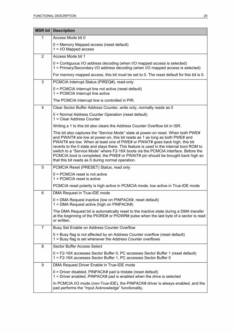
4.7.1.2 Mode and Control Register
MSR bit Description
0 ATA Mode bit
0 = PCMCIA ATA mode (reset default if POE# is high) 1 = True IDE mode (reset default if POE# is low)
This bit should not be changed by software. When the True-IDE detection enable bit is set in PIR, this bit falls back to 0 if POE# was low at reset time as soon as POE# changes back to high. When the True-IDE detection enable bit in PIR is cleared, this bit is not affected by changes of the POE# pin.
FUNCTIONAL DESCRIPTION 29
MSR bit Description
1 Access Mode bit 0
0 = Memory Mapped access (reset default) 1 = I/O Mapped access
2 Access Mode bit 1
0 = Contiguous I/O address decoding (when I/O mapped access is selected) 1 = Primary/Secondary I/O address decoding (when I/O mapped access is selected)
For memory mapped access, this bit must be set to 0. The reset default for this bit is 0.
3 PCMCIA Interrupt Status (PIREQ#), read-only
0 = PCMCIA Interrupt line not active (reset default) 1 = PCMCIA Interrupt line active
The PCMCIA Interrupt line is controlled in PIR.
4 Clear Sector Buffer Address Counter, write only, normally reads as 0
0 = Normal Address Counter Operation (reset default) 1 = Clear Address Counter
Writing a 1 to this bit also clears the Address Counter Overflow bit in ISR.
This bit also captures the “Service Mode” state at power-on reset. When both PWE# and PWAIT# are low at power-on, this bit reads as 1 as long as both PWE# and PWAIT# are low. When at least one of PWE# or PWAIT# goes back high, this bit reverts to the 0 state and stays there. This feature is used in the internal boot ROM to switch to a “Service Mode” where F2-16X boots via the PCMCIA interface. Before the PCMCIA boot is completed, the PWE# or PWAIT# pin should be brought back high so that this bit reads as 0 during normal operation.
5 PCMCIA Reset (PRESET) Status, read only
0 = PCMCIA reset is not active 1 = PCMCIA reset is active
PCMCIA reset polarity is high active in PCMCIA mode, low active in True-IDE mode
6 DMA Request in True-IDE mode
0 = DMA Request inactive (low on PINPACK#, reset default) 1 = DMA Request active (high on PINPACK#)
The DMA Request bit is automatically reset to the inactive state during a DMA transfer at the beginning of the PIORD# or PIOWR# pulse when the last byte of a sector is read or written.
7 Busy Set Enable on Address Counter Overflow
0 = Busy flag is not affected by an Address Counter overflow (reset default) 1 = Busy flag is set whenever the Address Counter overflows
8 Sector Buffer Access Select
0 = F2-16X accesses Sector Buffer 0, PC accesses Sector Buffer 1 (reset default) 1 = F2-16X accesses Sector Buffer 1, PC accesses Sector Buffer 0
9 DMA Request Driver Enable in True-IDE mode
0 = Driver disabled, PINPACK# pad is tristate (reset default) 1 = Driver enabled, PINPACK# pad is enabled when the drive is selected
In PCMCIA I/O mode (non-True-IDE), the PINPACK# driver is always enabled, and the pad performs the “Input Acknowledge” functionality.

30 FUNCTIONAL DESCRIPTION
MSR bit Description
10 State at the PINPACK# pad (True-IDE DMARQ), read only
0 = PINPACK# pad is low (DMARQ inactive) 1 = PINPACK# pad is high (DMARQ active)
11 State at the PREG# pad (True-IDE DMACK#), read only
0 = PREG# is high (DMACK inactive) 1 = PREG# is low (DMACK active)
12..14 Reserved
15 PCMCIA CIS Write Permission
0 = CIS (in Attribute Memory) is not writable from the host (reset default) 1 = CIS (in Attribute Memory) is writable from the host
At boot time, the Hyperstone F2-16X software must read out the ATA Mode bit and initialize the two access mode bits to memory-mapped mode for PCMCIA ATA mode and to Primary I/O mode in True IDE mode. The configuration index in the PCMCIA Configuration Option Register must be initialized to zero for PCMCIA ATA mode and to nonzero for True IDE mode.
4.7.1.3 True-IDE Mode Register
TIR bit Description
0 PDIAG (signal is on PSTSCHG#)
0 = PSTSCHG# pad is tristate (reset default) 1 = pull PSTSCHG# pad low
When read, this bit reflects the PSTSCHG# pad’s state (low reads as 1).
1 PDASP (signal is on PSPKR#)
0 = PSPKR# pad is tristate (reset default) 1 = pull PSPKR# pad low
When read, this bit reflects the PSPKR# pad’s state (low reads as 1).
2 Drive Select
0 = Drive selects as Master (reset default if PCSEL# is low) 1 = Drive selects as Slave (reset default if PCSEL# is high)
This bit must be initialized to 0 for the PCMCIA mode.
3 Drive 1 Status Register Read Enable
0 = Disable reading drive 1 status register (reset default) 1 = Enable reading drive 1 status register
This bit must be set in True IDE mode when our drive is configured as master with no slave present.
4 8 Bit Data Register Access Enable
0 = True-IDE data register access is 16 bit per transfer (reset default) 1 = True-IDE data register access is 8 bit per transfer
5 Multiple Controllers Master/Slave Select
0 = Single controller, or master with multiple controllers (reset default) 1 = Slave with multiple controllers

FUNCTIONAL DESCRIPTION 31
TIR bit Description
6 BUSRQ Line Control
0 = BUSRQ line is tristate, with pull-up on master (reset default) 1 = BUSRQ line is driven low
When read, this bit reflects the BUSRQ pad’s state (low reads as 1).
When multiple controllers are connected to the PCMCIA bus, exactly one of these must be the master, all others must be slave. The PCMCIA lines of a controller are driven if either
- a controller is master, and the BUSRQ line is high, or
- a controller is slave, and pulls the BUSRQ line low.
4.7.1.4 Interrupt Status Register
When any of the ISR bits is set, the processor’s INT1 or INT2 interrupts are activated. The interrupt service routine should read ISR, clear the bits it found set, and act upon them. A bit in ISR is cleared by writing a 1 bit into the appropriate bit position, writing a 0 bit to a bit position does not affect the bit’s value.
ISR bit Description
0 Configuration Register Write Interrupt
1 = The PCMCIA Configuration Option Register was written by the PCMCIA host.
1 Command Register Write Interrupt
1 = The ATA Command Register was written by the PCMCIA host.
The Command Register Write causes the Busy flag to be set.
2 Address Counter Overflow Interrupt
1 = The Sector Buffer Address Counter passed the end of the sector buffer.
This bit is also cleared by writing a 1 into MSR bit 4. The Address Counter overflow causes the Busy flag to be set if this is enabled in MSR bit 7.
3 PCMCIA Soft Reset was set Interrupt
1 = The Soft Reset bit was set in the ATA Device Control Register or in the PCMCIA Configuration Option Register.
The Soft Reset via the ATA Device Control Register causes the Busy flag to be set.
4 PCMCIA Soft Reset was cleared Interrupt
1 = The Soft Reset bit was cleared in the ATA Device Control Register or in the PCMCIA Configuration Option Register.
5 PCMCIA Power Down Request Interrupt
1 = The Power Down Request bit was set in the PCMCIA Card Configuration and Status Register
6 PCMCIA Reset (PRESET) was set Interrupt
1 = The PCMCIA Reset line was activated.
7 PCMCIA Reset (PRESET) was cleared Interrupt
1 = The PCMCIA Reset line was deactivated.
8..12 Flash Ready Interrupts 0..4
1 = Rising edge detected on address line A9..A13.

32 FUNCTIONAL DESCRIPTION
Any bit set in positions 0..7 of ISR activates interrupt INT1. Any bit set in positions 8..12 of ISR activates interrupt INT2.
4.7.1.5 PCMCIA Interrupt Register
PIR bit Description
0 Set PCMCIA Interrupt Request to the PCMCIA host (write only)
0 = No operation 1 = The PCMCIA Interrupt line is set.
Both the PCMCIA Interrupt line and the Interrupt bit in the PCMCIA Card Configuration and Status Register are reset when: - the ATA Status Register is read by the PCMCIA host - the ATA Command Register is written by the PCMCIA host - the PCMCIA Soft Reset was set Interrupt bit in ISR is set - and on a power-on reset.
1 Clear PCMCIA Interrupt Request to the PCMCIA host (write only)
0 = No operation 1 = The PCMCIA Interrupt line is reset.
2 Set Interrupt bit in the PCMCIA Card Configuration and Status Register (write only)
0 = No operation 1 = The Interrupt bit in the PCMCIA Card Configuration and Status Register is set.
3 Clear Interrupt bit in the PCMCIA Card Configuration and Status Register (write only)
0 = No operation 1 = The Interrupt bit in the PCMCIA Card Configuration and Status Register is cleared.
4..5 Unused
6 Set True-IDE Detection Enable
0 = No operation 1 = The True-IDE detection enable bit is set.
The True-IDE detection enable bit is set after power-on reset. As long as this bit is set, the True-IDE bit in MSR is reset to 0 as soon as a high (inactive) level is recognized on the POE# pin. When this bit is not reset, POE# activity does not affect the MSR True-IDE bit.
7 Clear True-IDE Detection Enable
0 = No operation 1 = The True-IDE detection enable bit is cleared.
4.7.2. Register Descriptions for the PCMCIA Registers
4.7.2.1 PCMCIA Configuration Register Access
The PCMCIA Configuration Registers can be accessed via internal I/O accesses by the F2-16X and via PCMCIA memory accesses by the PCMCIA host. Write access to these registers is guarded by the Busy flag: when Busy is set, the F2-16X may write the PCMCIA Configuration Registers, when Busy is clear, the PCMCIA host may write these registers.
For the PCMCIA host access to the PCMCIA configuration registers, an Attribute Memory read or write access is needed with an address of 20016, 20216, 20416 or 20616. These addresses select C1, C2, C3 and C4, respectively.

FUNCTIONAL DESCRIPTION 33
4.7.2.2 Configuration Option Register
C1 bit Description
5..0 Configuration Index
6 PCMCIA Interrupt Mode Select
0 = Pulse Mode Interrupts 1 = Level Mode Interrupts
7 PCMCIA Soft Reset
0 = Normal operation 1 = Software Reset
Any write access by the PCMCIA host to this register causes a Configuration Register Write Interrupt.
The F2-16X disables I/O accesses from the PCMCIA interface as long as the Configuration Index is zero. Prior to enabling the I/O interface in MSR, a Configuration Index unequal to zero must be written. This is done by the host (in PCMCIA mode) or must be done by the F2-16X (in True-IDE mode).
When the PCMCIA Soft Reset bit is changed, a PCMCIA Soft Reset interrupt is generated.
4.7.2.3 Card Configuration and Status Register
C2 bit Description
0 Reserved (0)
1 PCMCIA Interrupt (read only)
This bit is controlled by bits 0 and 2 of PIR.
2 PCMCIA Power Down Request
0 = Normal Operation 1 = Enter Power Down mode.
3 PCMCIA Audio
This bit is unused in F2-16X and should be set to 0.
4 Reserved (0)
5 PCMCIA IOis8
This bit should be set to 0 by the F2-16X since 16 bit I/O is possible.
6 Signal State Change
0 = State Changes (the Changed bit) should not be reported through PSTSCHG# 1 = State Changes are reported through the PSTSCHG# signal.
7 Changed (read only)
This bit represents the logical or of bits 4 to 7 of the Pin Replacement Register.
When the PCMCIA Power Down Request bit is set, a PCMCIA Power Down Request interrupt is generated.
4.7.2.4 Pin Replacement Register
All PCMCIA Pin Replacement Register bits can be written by the F2-16X. In order to conform to the PCMCIA protocol, every time a bit from bits 0 to 3 is set, the corresponding bit in bits 4 to 7 must be set by the F2-16X. This can be done by a read-
34 FUNCTIONAL DESCRIPTION
modify-write cycle since write accesses to the Pin Replacement Register are guarded by the Busy signal. When a bit from bits 0 to 3 is reset, the corresponding bit in bits 4..7 must not be changed.
The PCMCIA host has no write access to bits 0 to 3. Bits 4 to 7 can be written by the PCMCIA host through a write mask in the corresponding bit of bits 0 to 3: for example, if the PCMCIA host performs a write access to the Pin Replacement Register with data bits 1 and 2 set, bits 5 and 6 of the Pin Replacement Register are written with the data bits 5 and 6 from the PCMCIA host, and bits 0 to 3, 4 and 7 are not changed by this write access.
C3 bit Description
0 Write Protect
This bit is used to generate the WP signal (PIOIS16# pin) in memory-mapped mode.
1 Ready/-Busy
2 Battery Voltage Detect 2 (set to 0 when no battery is there)
3 Battery Voltage Detect 1 (set to 0 when no battery is there)
4 Changed Write Protect
5 Changed Ready/-Busy
6 Changed Battery Voltage Detect 2
7 Changed Battery Voltage Detect 1
4.7.2.5 Socket and Copy Register
C4 bit Description
3..0 Socket Number
6..4 Copy Number
7 Reserved (0)
4.7.3. Register Descriptions for the ATA Task File Registers
4.7.3.1 ATA Task File Register Access
The ATA Task File Registers can be accessed by the F2-16X using internal I/O accesses and by the PCMCIA host using I/O or memory accesses on the PCMCIA interface. See section 4.8 Register and Sector Buffer Access Modes for details.
4.7.3.2 ATA Feature Register
A01 bit Description
7..0 Command Specific
4.7.3.3 ATA Sector Count Register
A02 bit Description
7..0 Sector Count for read or write operation. Sector Count 0 means 256 sectors.
FUNCTIONAL DESCRIPTION 35
4.7.3.4 ATA Sector Number Register
A03 bit Description
7..0 Sector Number for the next command, range 1 to max. number of sectors per track. LBA bits 7..0 in LBA addressing mode.
4.7.3.5 ATA Cylinder Low Register
A04 bit Description
7..0 Bits 7..0 of the starting cylinder number for the next command. LBA bits 15..8 in LBA addressing mode.
4.7.3.6 ATA Cylinder High Register
A05 bit Description
7..0 Bits 15..8 of the starting cylinder number for the next command. LBA bits 23..16 in LBA addressing mode.
4.7.3.7 ATA Drive/Head Register
A06 bit Description
3..0 Head number to select for the next command (0..15). LBA bits 27..24 in LBA mode.
4 Drive 0 select (0) or Drive 1 select (1)
5 Reserved (1)
6 Addressing Mode select
0 = addressing is by Cylinder/Head/Sector (CHS mode) 1 = addressing is by LBA mode
7 Reserved (1)
4.7.3.8 ATA Command Register
A PCMCIA write access to the ATA Command Register causes the Busy flag to be set and generates a Command Register Write Interrupt.
A07 bit Description
7..0 Command Code for the next command to be executed.
4.7.3.9 ATA Status Register, ATA Alternate Status Register
The ATA Status Register and the ATA Alternate Status Register carry the same information. The only difference is, reading the ATA Status Register implies an interrupt acknowledge and resets the PCMCIA Interrupt line while reading the ATA Alternate Status Register does not.

36 FUNCTIONAL DESCRIPTION
A00 bit Description
0 ERR (Error). An error occurred during command execution, further information can be found in the Error Register
1 IDX (Index).
2 CORR (Corrected Data). A correctable data error occurred and the data has been corrected.
3 DRQ (Data Request). The drive is ready to transfer data. This bit is cleared when a host Data Register access causes an Address Counter overflow.
4 DSC (Drive Seek Complete).
5 DWF (Drive Write Fault)
6 DRDY (Drive Ready). The drive is ready to accept a command.
7 BSY (Busy). This bit indicates that the drive has access to the ATA Registers. When any ATA register is read by the PCMCIA host, the Status Register content is returned.
The F2-16X hardware sets the Busy flag on any of the following events: power-up reset any PCMCIA write access to the ATA Command Register the Soft Reset bit in the ATA Device Control Register is being set sector buffer address counter overflow when MSR bit 7 is set.
4.7.3.10 ATA Error Register
A08 bit Description
7..0 Status from the last command, valid when the ERR bit in the ATA Status Register is set. Diagnostic code from Execute Drive Diagnostics command.
4.7.3.11 ATA Device Control Register
A10 bit Description
0 Reserved (0)
1 nIEN (negated Interrupt Enable). This bit is initialized to 0 on power-on reset and on PCMCIA reset assertion.
0 = Interrupt is enabled 1 = Interrupt is disabled
2 SRST (Soft Reset). This bit is initialized to 0 on reset.
3 Reserved (1)
The PCMCIA Interrupt line is used as Ready/-Busy output in memory-mapped mode. In I/O mode, the interrupt line state is determined by the PCMCIA Interrupt bit that is set or reset by PIR bits 0 and 1 and queried in MSR bit 5. In PCMCIA I/O mode, the interrupt line is always driven (active high) according to the PCMCIA Interrupt bit. In True-IDE mode, the interrupt line is driven (active low) according to the PCMCIA Interrupt bit when the drive is selected (bit 4 in the ATA Drive/Head Register equals bit 2 in TIR), else the interrupt line is tristate.
When the SRST bit is being set by the PCMCIA host, the Busy flag is set and a PCMCIA Soft Reset was set Interrupt is generated. When this bit is being cleared by the PCMCIA host, a PCMCIA Soft Reset was cleared Interrupt is generated.
FUNCTIONAL DESCRIPTION 37
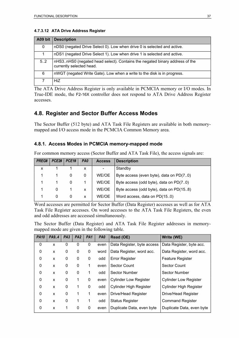
4.7.3.12 ATA Drive Address Register
A09 bit Description
0 nDS0 (negated Drive Select 0). Low when drive 0 is selected and active.
1 nDS1 (negated Drive Select 1). Low when drive 1 is selected and active.
5..2 nHS3..nHS0 (negated head select). Contains the negated binary address of the currently selected head.
6 nWGT (negated Write Gate). Low when a write to the disk is in progress.
7 HiZ
The ATA Drive Address Register is only available in PCMCIA memory or I/O modes. In True-IDE mode, the F2-16X controller does not respond to ATA Drive Address Register accesses.
4.8. Register and Sector Buffer Access Modes
The Sector Buffer (512 byte) and ATA Task File Registers are available in both memory-mapped and I/O access mode in the PCMCIA Common Memory area.
4.8.1. Access Modes in PCMCIA memory-mapped mode
For common memory access (Sector Buffer and ATA Task File), the access signals are: PREG# PCE2# PCE1# PA0 Access Description
x 1 1 x - Standby
1 1 0 0 WE/OE Byte access (even byte), data on PD(7..0)
1 1 0 1 WE/OE Byte access (odd byte), data on PD(7..0)
1 0 1 x WE/OE Byte access (odd byte), data on PD(15..8)
1 0 0 x WE/OE Word access, data on PD(15..0)
Word accesses are permitted for Sector Buffer (Data Register) accesses as well as for ATA Task File Register accesses. On word accesses to the ATA Task File Registers, the even and odd addresses are accessed simultaneously.
The Sector Buffer (Data Register) and ATA Task File Register addresses in memory-mapped mode are given in the following table.
PA10 PA9..4 PA3 PA2 PA1 PA0 Read (OE) Write (WE)
0 x 0 0 0 even Data Register, byte access Data Register, byte acc.
0 x 0 0 0 word Data Register, word acc. Data Register, word acc.
0 x 0 0 0 odd Error Register Feature Register
0 x 0 0 1 even Sector Count Sector Count
0 x 0 0 1 odd Sector Number Sector Number
0 x 0 1 0 even Cylinder Low Register Cylinder Low Register
0 x 0 1 0 odd Cylinder High Register Cylinder High Register
0 x 0 1 1 even Drive/Head Register Drive/Head Register
0 x 0 1 1 odd Status Register Command Register
0 x 1 0 0 even Duplicate Data, even byte Duplicate Data, even byte
38 FUNCTIONAL DESCRIPTION
PA10 PA9..4 PA3 PA2 PA1 PA0 Read (OE) Write (WE)
0 x 1 0 0 odd Duplicate Data, odd byte Duplicate Data, odd byte
0 x 1 0 0 word Duplicate Data Duplicate Data
0 x 1 1 0 odd Duplicate Error Register Duplicate Error Register
0 x 1 1 1 even Alternate Status Register Device Control Register
0 x 1 1 1 odd Drive Address Register -
1 x x x x even Data Register, even byte Data Register, even byte
1 x x x x odd Data Register, odd byte Data Register, odd byte
1 x x x x word Data Register Data Register
For Attribute Memory (CIS and PCMCIA Configuration Registers), only even addresses are valid. The access signals are:
PREG# PCE2# PCE1# PA0 Access Description
x 1 1 x - Standby
0 1 0 0 WE/OE Byte access (even byte), data on PD(7..0)
0 1 0 1 WE/OE not valid
0 0 1 x WE/OE not valid
0 0 0 x WE/OE Word access, even byte data on PD(7..0)
The Attribute Memory (Card Information Structure) and PCMCIA Configuration Register addresses in memory-mapped mode are given in the following table.
PA9 PA8..3 PA2 PA1 PA0 Description
0 8 bit address even 256 bytes Card Information Structure
1 x 0 0 even PCMCIA Configuration Option Register (C1) 1 x 0 1 even PCMCIA Card Configuration and Status Register (C2) 1 x 1 0 even PCMCIA Pin Replacement Register (C3) 1 x 1 1 even PCMCIA Socket and Copy Register (C4)
Write accesses to the Card Information Structure are only possible if the PCMCIA CIS Write Permission bit in MSR is set.
4.8.2. Access Modes in PCMCIA I/O mode
In I/O mode, common and attribute memory access signals are: PREG# PCE2# PCE1# PA0 Access Description
x 1 1 x - Standby
0 1 0 0 IOWR/RD Byte access (even byte), data on PD(7..0)
1 0 1 IOWR/RD Byte access (odd byte), data on PD(7..0)
0 0 1 x IOWR/RD Byte access (odd byte), data on PD(15..8)
0 0 0 x IOWR/RD Word access, data on PD(15..0)
0

FUNCTIONAL DESCRIPTION 39
PREG# PCE2# PCE1# PA0 Access Description
0 x x x WE/OE Attribute Memory access, see memory-mapped mode
Word accesses are permitted for Sector Buffer (Data Register) accesses as well as for ATA Task File Register accesses. On word accesses to the ATA Task File Registers, the even and odd addresses are accessed simultaneously.
The Sector Buffer (Data Register) and ATA Task File Register addresses in Contiguous I/O mode are given in the following table.
PA3 PA2 PA1 PA0 Read (IORD) Write (IOWR)
0 0 0 even Data Register, byte access Data Register, byte access
0 0 0 word Data Register, word access Data Register, word access
0 0 0 odd Error Register Feature Register
0 0 1 even Sector Count Sector Count
0 0 1 odd Sector Number Sector Number
0 1 0 even Cylinder Low Register Cylinder Low Register
0 1 0 odd Cylinder High Register Cylinder High Register
0 1 1 even Drive/Head Register Drive/Head Register
0 1 1 odd Status Register Command Register
1 0 0 even Duplicate Data, even byte Duplicate Data, even byte
1 0 0 odd Duplicate Data, odd byte Duplicate Data, odd byte
1 0 0 word Duplicate Data Duplicate Data
1 1 0 odd Duplicate Error Register Duplicate Error Register
1 1 1 even Alternate Status Register Device Control Register
1 1 1 odd Drive Address Register -
The Sector Buffer (Data Register) and ATA Task File Register addresses in Primary or Secondary I/O mode are given in the following table.
PA9 PA2 PA1 PA0 Read (IORD) Write (IOWR)
0 0 0 even Data Register, byte access Data Register, byte access
0 0 0 word Data Register, word access Data Register, word access
0 0 0 odd Error Register Feature Register
0 0 1 even Sector Count Sector Count
0 0 1 odd Sector Number Sector Number
0 1 0 even Cylinder Low Register Cylinder Low Register
0 1 0 odd Cylinder High Register Cylinder High Register
0 1 1 even Drive/Head Register Drive/Head Register
0 1 1 odd Status Register Command Register
1 1 1 even Alternate Status Register Device Control Register
1 1 1 odd Drive Address Register -

40 FUNCTIONAL DESCRIPTION
4.8.3. Access Modes in True-IDE mode
In True-IDE mode, only common memory (Sector Buffer and ATA Task File) is addressable. The access signals are:
PREG# PCE2# PCE1# Access Description
x 1 1 - Standby
x 1 0 IOWR/RD ATA Command block access (Cmd in table below)
x 0 1 IOWR/RD ATA Control block access (Ctrl in table below)
x 0 0 IOWR/RD not valid
A word access is valid only for the Sector Buffer (Data Register) access.
The Sector Buffer (Data Register) and ATA Task File Register addresses in True-IDE Primary or Secondary I/O mode are given in the following table.
Block PA2 PA1 PA0 Read (IORD) Write (IOWR)
Cmd 0 0 0 Data Register, word access Data Register, word access
Cmd 0 0 1 Error Register Feature Register
Cmd 0 1 0 Sector Count Sector Count
Cmd 0 1 1 Sector Number Sector Number
Cmd 1 0 0 Cylinder Low Register Cylinder Low Register
Cmd 1 0 1 Cylinder High Register Cylinder High Register
Cmd 1 1 0 Drive/Head Register Drive/Head Register
Cmd 1 1 1 Status Register Command Register
Ctrl 1 1 0 Alternate Status Register Device Control Register
The Drive Address Register is not available in True-IDE mode.
4.9. Hyperstone Sector Buffer Access
The sector buffers and the attribute memory are available on the Hyperstone side in the IRAM access space, starting at C800 000016. There are two sector buffers of 528 bytes (132 words of 32 bits), and a 256 byte attribute memory. Read accesses to these memories are unrestricted, write accesses must always be in 32 bit units (byte or halfword write accesses are not allowed).
The selection which of the sector buffers are accessed from the Hyperstone side and from the host side depends on the Sector Buffer Select bit in MCR, and on the Busy state. The access modes are detailed in the following table. When Busy is 0, the host side (PCMCIA) always has access to sector buffer SB0 when MSR(8) is 1, and to sector buffer SB1 when MSR(8) is 0.
The 256 byte attribute memory is mapped to 256 words in this address range, with the 8 bit data in bits 31..24 of these words.

FUNCTIONAL DESCRIPTION 41
Hyperstone Address Bits Busy
15 14 13 12 11 10 9 8 7 6 5 4 3 2 1 0
Hy Access MSR(8)=0
Hy Access MSR(8)=1
0 0 x 0 x x 0 528 byte SB0 SB1
0 X x x x x 1 x x x x x x x x x x
0 x x 1 x x x x x x x x x x x x x
0 1 x x x x x x x x x x x x x x x
1 0 x 0 x x 0 528 byte SB0 SB1
1 0 x 0 x x 1 528 byte SB1 SB0
1 0 x 1 x x 0 528 byte SB0
1 0 x 1 x x 1 528 byte SB1
1 1 x x x x x 256 byte 0 0 Attribute Memory
4.10. Internal ROM
The F2-16X has 8 Kbytes of internal ROM at address D000 000016 with a wraparound modulo 8 Kbytes up to DFFF FFFF16. When the interrupt 4 input of the F2-16X is low (or open) at reset, the reset trap begins executing the internal boot ROM code at DFFF FFF816.
The internal ROM present on the F2-16X performs the following actions on reset when booting is done from ROM:
The F2-16X processor is initialized.
IO(3) is switched to output driving 0 (for Samsung Flashes) or 1 (for Hitachi Flashes), FCR bit 7 (Flash Select) is initialized according to the detected Flash type. After 50 µs delay for the stabilization of the voltage regulator, all Flashes are deselected and IO(2) (Flash Write Protect) is switched to output driving 1 so that Flash access is possible.
The Busy flag is set in the ATA Status Register. The PCMCIA and ATA Registers are initialized to allow a PCMCIA boot if a power-on reset is detected.
If the PWE# and PWAIT# pins were low at reset and still are, the F2-16X tries to boot from PCMCIA. Else, the F2-16X tries to boot from Flash 0. This involves a search of the Anchor Block and a load of the Main Program and Overlay sectors. If the Anchor Block is not found or if there is an uncorrectable error when loading the program, the F2-16X falls back to booting from PCMCIA. If the Anchor Block is found, a copy is stored in the sector buffer SB1 Then, a pre-boot routine at offset 01FC16 in SB1 is called. After return, the F2-16X processor proceeds to load the Program and Overlay sectors from Flash 0 using the Anchor Block information in sector buffer SB1.
For the PCMCIA boot, the F2-16X determines the device ID of flash chip 0 and stores this information in the cylinder high and low registers. Then, the F2-16X writes B816 into the ATA Error register and sets DRDY, DSC and ERR in the ATA Status register. The boot software on the host must then respond by writing the number of sectors (512 bytes) to boot into the ATA Sector Count register and 8016 into the ATA Command register. The F2-16X then reads the specified number of sectors by setting DRDY, DRQ and DSC in the ATA Status register. The downloaded code is put into IRAM starting at address C000 000016.

42 ELECTRICAL SPECIFICATIONS
5. Electrical Specifications
5.1. DC Characteristics
5.1.1. Absolute Maximum Ratings
Case temperature TC under Bias: 0°C to +85°C -40°C to +85°C for F2-IL16XN
Storage Temperature: -65°C to +150°C
Voltage on any Pin with respect to ground: -0.5V to VCC + 0.5V
5.1.2. D.C. Parameters
Supply Voltage VCC_P and VCC_R: 5V ± 0.5V or 3.3V ± 0.30V
Supply Voltage VCC_F: 3.3V ± 0.30V
Supply Voltage VCC_C: 2.5V ± 0.25V
Case Temperature TCASE: 0°C to +85°C
Symbol Parameter Min Max Units Notes
VIL Input LOW Voltage -0.3 +0.8 V
VIH Input HIGH Voltage 2.0 VCC+0.3 V
VOL Output LOW Voltage 0.45 V at 4mA
VOH Output HIGH Voltage 2.4 V at 1mA
ICC Operating Current, VCC_R=5.0V
Sleep mode Operating, 20 MHz Operating, 40 MHz
0.2 30 50
mA mA mA
ICC Operating Current, VCC_R=3.3V
Sleep mode Operating, 20 MHz Operating, 40 MHz
0.2 30 50
mA mA mA
ILI Input Leakage Current ±10 µA
ILO Output Leakage Current ±10 µA
CI/O Input/output Capacitance 10 pF
Table 2: DC Characteristics
ELECTRICAL SPECIFICATIONS 43
5.2. AC Characteristics
The AC Characteristics reference the timing diagrams of the PCMCIA PC Card Standard and the symbols in these timing diagrams. The AC characteristics are valid for a supply voltage VCC of 5V ± 10% or 3.3V ± 5%.
5.2.1. Attribute Memory Read and Write AC Characteristics
Symbol Parameter Min Max Units
tcR Read cycle time 250 ns
ta(A) Address access time 250 ns
ta(CE) Card Enable access time 250 ns
ta(OE) Output Enable access time 125 ns
tdis(CE) Output disable time from CE 100 ns
tdis(OE) Output disable time from OE 100 ns
ten(CE) Output enable time from CE 5 ns
ten(OE) Output enable time from OE 5 ns
tv(A) Data valid time from address change
0 ns
tsu(A) Address setup time 30 ns
th(A) Address hold time 20 ns
tsu(CE) Card Enable setup time 0 ns
th(CE) Card Enable hold time 20 ns
tcW Write cycle time 250 ns
tw(WE) Write pulse time 150 ns
tsu(A-WEH) Address setup time for WE 180 ns
tsu(CE-WEH) Card Enable setup time for WE 180 ns
tsu(D-WEH) Data setup time for WE 80 ns
th(D) Data hold time 30 ns
tdis(WE) Output disable time from WE 100 ns
ten(WE) Output enable time from WE 5 ns
tsu(OE-WE) Output Enable setup time for WE 10 ns
th(OE-WE) Output Enable hold time from WE 10 ns
Table 3: Attribute Memory Read and Write AC Characteristics
44 ELECTRICAL SPECIFICATIONS
5.2.2. Common Memory Read and Write AC Characteristics
Symbol Parameter Min Max Units
tcR Read cycle time 150 ns
ta(A) Address access time 150 ns
ta(CE) Card Enable access time 150 ns
ta(OE) Output Enable access time 75 ns
tdis(CE) Output disable time from CE 75 ns
tdis(OE) Output disable time from OE 75 ns
ten(CE) Output enable time from CE 5 ns
ten(OE) Output enable time from OE 5 ns
tv(A) Data valid time from address change
0 ns
tsu(A) Address setup time 20 ns
th(A) Address hold time 20 ns
tsu(CE) Card Enable setup time 0 ns
th(CE) Card Enable hold time 20 ns
tcW Write cycle time 150 ns
tw(WE) Write pulse time 80 ns
tsu(A-WEH) Address setup time for WE 100 ns
tsu(CE-WEH) Card Enable setup time for WE 100 ns
tsu(D-WEH) Data setup time for WE 50 ns
th(D) Data hold time 20 ns
trec(WE) Write recover time 20 ns
tdis(WE) Output disable time from WE 75 ns
ten(WE) Output enable time from WE 5 ns
tsu(OE-WE) Output Enable setup time for WE 10 ns
th(OE-WE) Output Enable hold time from WE 10 ns
Table 4: Common memory Read and Write AC Characteristics

ELECTRICAL SPECIFICATIONS 45
5.2.3. I/O Access Read and Write AC Characteristics
Symbol Parameter Min Max Units
td(IORD) Data delay after IORD 100 ns
th(IORD) Data hold following IORD 0 ns
tw(IORD) IORD pulse width 165 ns
tsuA(IORD) Address setup time for IORD 70 ns
thA(IORD) Address hold time from IORD 20 ns
tsuCE(IORD) Card Enable setup time for IORD 5 ns
thCE(IORD) Card Enable hold time from IORD 20 ns
tsuREG(IORD) REG setup time for IORD 5 ns
thREG(IORD) REG hold time from IORD 0 ns
tdfINP(IORD) INPACK delay falling from IORD 0 45 ns
tdrINP(IORD) INPACK delay rising from IORD 45 ns
tdfIO16(IORD) IOIS16 delay falling from address 35 ns
tdrIO16(IORD) IOIS16 delay rising from address 35 ns
tsu(IOWR) Data setup time for IOWR 60 ns
th(IOWR) Data hold time from IOWR 30 ns
tw(IOWR) IOWR pulse width 165 ns
tsuA(IOWR) Address setup time for IOWR 70 ns
thA(IOWR) Address hold time from IOWR 20 ns
tsuCE(IOWR) Card Enable setup time for IOWR 5 ns
thCE(IOWR) Card Enable hold time from IOWR 20 ns
tsuREG(IOWR) REG setup time for IOWR 5 ns
thREG(IOWR) REG hold time from IOWR 0 ns
Table 5: I/O Access Read and Write AC Characteristics

46 ELECTRICAL SPECIFICATIONS
5.2.4. True-IDE Mode I/O Access Read and Write AC Characteristics
Symbol Parameter Min Max Units
tcR Cycle time 120 ns
tsuA Address setup time for IORD/IOWR 25 ns
thA Address hold time from IORD/IOWR 10 ns
tw IORD/IOWR pulse width 70 ns
trec IORD/IOWR recovery time 25 ns
tsuD(IORD) Data setup time for IORD 20 ns
thD(IORD) Data hold following IORD 5 ns
tdis(IORD) Output disable time from IORD 30 ns
tsuD(IOWR) Data setup time for IOWR 20 ns
thD(IOWR) Data hold following IOWR 10 ns
Table 6: True-IDE Mode I/O Access Read and Write AC Characteristics
5.2.5. Flash Memory Interface AC Characteristics, Samsung Type
The AC Characteristics for the flash memory interface are based on a F2-16X processor clock speed of 20 MHz.
Symbol Parameter Min Max Units
tCLS CLE setup time 50 ns
tCLH CLE hold time 20 ns
tCS CE setup time 50 ns
tCH CE hold time 50 ns
tWP WE pulse width 25 ns
tALS ALE setup time 50 ns
tALH ALE hold time 20 ns
tDS Data Setup time 25 ns
tDH Data hold time 20 ns
tWC Write cycle time 50 ns
tWH WE high hold time 20 ns
tRP RE pulse width 30 ns
tRC Read cycle time 50 ns
tREA RE access time 35 ns
tREH RE high hold time 15 ns
tCEH CE high hold time 200 ns
tWHR WE high to RE low 100 ns
Table 7: AC Characteristics for Samsung Type flash memory

47
Hyperstone AG Line-Eid-Straße 3 D-78467 Konstanz Germany Phone +49 – 7531 - 98030 Fax +49 – 7531 - 51725 E-Mail [email protected]
http://www.hyperstone.com
Related Documents