Hybrid cascode feedforward compensation for nano-scale low-power ultra-area-efficient three-stage amplifiers Hamed Aminzadeh a,n , Mohammad Danaie b , Wouter A. Serdijn c a Department of Electrical Engineering, Payame Noor University, 19395-3697 Tehran, Iran b Faculty of Electrical and Computer Engineering, Semnan University, Semnan, Iran c Electronics Research Laboratory, Delft University of Technology, Delft 56101, The Netherlands article info Article history: Received 29 March 2013 Received in revised form 2 August 2013 Accepted 6 August 2013 Keywords: Cross-feedforward cascode compensation Frequency compensation Hybrid cascode feedforward compensation Low power Nested-Miller compensation Operational amplifier (opamp) Single-Miller feedforward compensation and stability abstract A modified frequency compensation technique is proposed for low-power area-efficient three-stage amplifiers driving medium to large capacitive loads. Coined hybrid cascode feedforward compensation (HCFC), the total compensation capacitor is divided and shared between two internal high-speed feedback loops instead of only one loop as is common in prior art. Detailed analysis of this technique shows significant improvement in terms of bandwidth and stability. This is verified for a 1.2-V amplifier driving a 500-pF capacitive load in 90-nm CMOS technology, where HCFC reduces the total capacitor size and improves the gain-bandwidth by at least 30% and 40% respectively, compared to the prevailing schemes. & 2013 Elsevier Ltd. All rights reserved. 1. Introduction Frequency compensation is a conventional design step in the design procedure for negative-feedback amplifiers used in drivers, filters, data converters and low-dropout regulators [1–17]. Depend- ing on the load capacitor (C L ), a minimum compensation capacitor (C C ) is required to maintain stability, by which the gain-bandwidth (GBW) and slew-rate (SR) are affected depending on their value. With two large compensation capacitors proportional to C L , the well-known nested Miller compensation (NMC) [1–3] fails to achieve sufficient GBW and SR under low power constraints. Various frequency compensation strategies have therefore been proposed to reduce the size of the compensation capacitors with limited power budget. Multipath nested Miller compensation (MNMC) [6] compen- sation is among these solutions which aims to further push away the power/area envelope. It uses a feedforward stage to implant an additional left-half-plane (LHP) zero to the NMC transfer function. The undesired right-half plane (RHP) zero in basic NMC architecture imposes excessive power for sufficient stability. Nested Gm-C com- pensation is another compensation solution dedicated for three- stage amplifiers to remove this RHP zero [7]. Looking for ways to remove the bulky capacitance used within the internal ac feedback loop of the NMC has also been the idea of some improved architectures. This capacitance is used to control the location of the complex poles for adequate gain margin (GM). The damping-factor- control frequency compensation (DFCFC) [8] replaces this capacitor with an active damping-factor-control unit. As a step further, the main compensation capacitor is substituted with an active capaci- tance in active feedback frequency compensation (AFFC) [9], resulting in improved stability with lower compensation capacitance. The remaining passive capacitance in AFFC is replaced by a damping- factor-control unit in dual-loop parallel compensation (DLPC) [10]. Two high-speed paths are also included to extend the bandwidth and to reduce the capacitor [10]. A serial RC network is added at the output of the amplifier intermediate stage to create a LHP zero in impedance adapting compensation (IAC) [11]. A standard Miller capacitance is also used for pole-splitting. Combining the concepts of signal feedforwarding and pole-splitting, single Miller capacitor feedforward frequency compensation (SMFFC) successfully removes the second compensation capacitance in NMC topology [12]. As proposed, the sizing of the remaining capacitance can also be decreased when increasing the gain of the intermediate stage [12]. To stabilize the amplifiers driving ultra-large capacitive loads, a few compensation techniques have been reported so far. Among these solutions are single capacitor with current amplifier compen- sation (SCCAC) [13], and current-buffer Miller compensation (CBMC) plus parasitic-pole cancellation [14,15]. Contents lists available at ScienceDirect journal homepage: www.elsevier.com/locate/mejo Microelectronics Journal 0026-2692/$ - see front matter & 2013 Elsevier Ltd. All rights reserved. http://dx.doi.org/10.1016/j.mejo.2013.08.004 n Corresponding author. E-mail addresses: [email protected], [email protected] (H. Aminzadeh), [email protected] (M. Danaie), [email protected] (W.A. Serdijn). Please cite this article as: H. Aminzadeh, et al., Hybrid cascode feedforward compensation for nano-scale low-power ultra-area-efficient three-stage amplifiers, Microelectron. J (2013), http://dx.doi.org/10.1016/j.mejo.2013.08.004i Microelectronics Journal ∎ (∎∎∎∎) ∎∎∎–∎∎∎

Welcome message from author
This document is posted to help you gain knowledge. Please leave a comment to let me know what you think about it! Share it to your friends and learn new things together.
Transcript
Hybrid cascode feedforward compensation for nano-scale low-powerultra-area-efficient three-stage amplifiers
Hamed Aminzadeh a,n, Mohammad Danaie b, Wouter A. Serdijn c
a Department of Electrical Engineering, Payame Noor University, 19395-3697 Tehran, Iranb Faculty of Electrical and Computer Engineering, Semnan University, Semnan, Iranc Electronics Research Laboratory, Delft University of Technology, Delft 56101, The Netherlands
a r t i c l e i n f o
Article history:Received 29 March 2013Received in revised form2 August 2013Accepted 6 August 2013
Keywords:Cross-feedforward cascode compensationFrequency compensationHybrid cascode feedforward compensationLow powerNested-Miller compensationOperational amplifier (opamp)Single-Miller feedforward compensationand stability
a b s t r a c t
A modified frequency compensation technique is proposed for low-power area-efficient three-stageamplifiers driving medium to large capacitive loads. Coined hybrid cascode feedforward compensation(HCFC), the total compensation capacitor is divided and shared between two internal high-speedfeedback loops instead of only one loop as is common in prior art. Detailed analysis of this techniqueshows significant improvement in terms of bandwidth and stability. This is verified for a 1.2-V amplifierdriving a 500-pF capacitive load in 90-nm CMOS technology, where HCFC reduces the total capacitor sizeand improves the gain-bandwidth by at least 30% and 40% respectively, compared to the prevailingschemes.
& 2013 Elsevier Ltd. All rights reserved.
1. Introduction
Frequency compensation is a conventional design step in thedesign procedure for negative-feedback amplifiers used in drivers,filters, data converters and low-dropout regulators [1–17]. Depend-ing on the load capacitor (CL), a minimum compensation capacitor(CC) is required to maintain stability, by which the gain-bandwidth(GBW) and slew-rate (SR) are affected depending on their value.With two large compensation capacitors proportional to CL, thewell-known nested Miller compensation (NMC) [1–3] fails toachieve sufficient GBW and SR under low power constraints. Variousfrequency compensation strategies have therefore been proposed toreduce the size of the compensation capacitors with limited powerbudget. Multipath nested Miller compensation (MNMC) [6] compen-sation is among these solutions which aims to further push away thepower/area envelope. It uses a feedforward stage to implant anadditional left-half-plane (LHP) zero to the NMC transfer function.The undesired right-half plane (RHP) zero in basic NMC architectureimposes excessive power for sufficient stability. Nested Gm-C com-pensation is another compensation solution dedicated for three-stage amplifiers to remove this RHP zero [7]. Looking for ways to
remove the bulky capacitance used within the internal ac feedbackloop of the NMC has also been the idea of some improvedarchitectures. This capacitance is used to control the location of thecomplex poles for adequate gain margin (GM). The damping-factor-control frequency compensation (DFCFC) [8] replaces this capacitorwith an active damping-factor-control unit. As a step further, themain compensation capacitor is substituted with an active capaci-tance in active feedback frequency compensation (AFFC) [9], resultingin improved stability with lower compensation capacitance. Theremaining passive capacitance in AFFC is replaced by a damping-factor-control unit in dual-loop parallel compensation (DLPC) [10].Two high-speed paths are also included to extend the bandwidthand to reduce the capacitor [10]. A serial RC network is added at theoutput of the amplifier intermediate stage to create a LHP zero inimpedance adapting compensation (IAC) [11]. A standard Millercapacitance is also used for pole-splitting. Combining the conceptsof signal feedforwarding and pole-splitting, single Miller capacitorfeedforward frequency compensation (SMFFC) successfully removesthe second compensation capacitance in NMC topology [12]. Asproposed, the sizing of the remaining capacitance can also bedecreased when increasing the gain of the intermediate stage [12].
To stabilize the amplifiers driving ultra-large capacitive loads,a few compensation techniques have been reported so far. Amongthese solutions are single capacitor with current amplifier compen-sation (SCCAC) [13], and current-buffer Miller compensation (CBMC)plus parasitic-pole cancellation [14,15].
Contents lists available at ScienceDirect
journal homepage: www.elsevier.com/locate/mejo
Microelectronics Journal
0026-2692/$ - see front matter & 2013 Elsevier Ltd. All rights reserved.http://dx.doi.org/10.1016/j.mejo.2013.08.004
n Corresponding author.E-mail addresses: [email protected],
[email protected] (H. Aminzadeh), [email protected] (M. Danaie),[email protected] (W.A. Serdijn).
Please cite this article as: H. Aminzadeh, et al., Hybrid cascode feedforward compensation for nano-scale low-power ultra-area-efficientthree-stage amplifiers, Microelectron. J (2013), http://dx.doi.org/10.1016/j.mejo.2013.08.004i
Microelectronics Journal ∎ (∎∎∎∎) ∎∎∎–∎∎∎
The available compensation solutions some of which reportedabove considerably reduce the size of the compensation network,yet, unless consuming significant power, this block still remainsas one of the largest parts of the integrated negative-feedbackamplifiers [5–15].
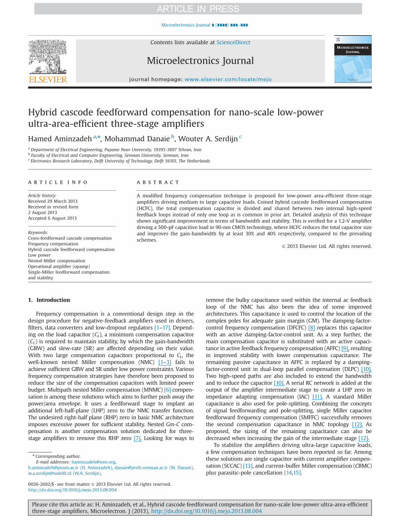
Cross feedforward cascode compensation (CFCC) [16] is one of therecently-proposed effective solutions to decrease the size of thecompensation capacitance in a three-stage operational amplifier. Incomparison with other topologies based on the required capacitancevalue, power consumption, and design complexity, it shows betterperformance metrics for capacitive loads up to a few nano-farads [5–16]. Fig. 1 depicts a three-stage amplifier with one compensationcapacitance either in SMFFC or CFCC configurations. Compared toadvanced variations of NMC, SMFFC needs less area for implementa-tion as the required CC is divided by the gain of the intermediate stage[12]. A transconductance (gm)-stage (gmC) in series with the compen-sation capacitance further decreases the required area in accordancewith the results from CFCC [16]. This makes CC a function of
ffiffiffiffiffiCL
p
rather than CL in SMFFC that is considerably effective especially forlarger capacitive loads.
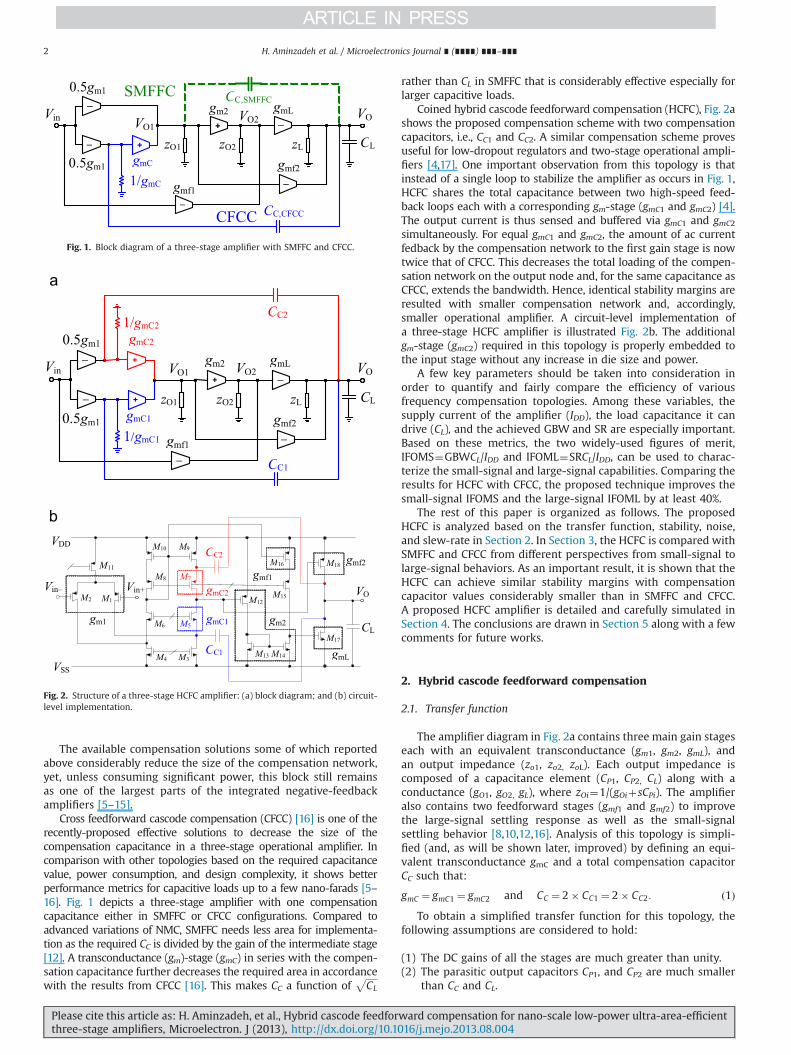
Coined hybrid cascode feedforward compensation (HCFC), Fig. 2ashows the proposed compensation scheme with two compensationcapacitors, i.e., CC1 and CC2. A similar compensation scheme provesuseful for low-dropout regulators and two-stage operational ampli-fiers [4,17]. One important observation from this topology is thatinstead of a single loop to stabilize the amplifier as occurs in Fig. 1,HCFC shares the total capacitance between two high-speed feed-back loops each with a corresponding gm-stage (gmC1 and gmC2) [4].The output current is thus sensed and buffered via gmC1 and gmC2
simultaneously. For equal gmC1 and gmC2, the amount of ac currentfedback by the compensation network to the first gain stage is nowtwice that of CFCC. This decreases the total loading of the compen-sation network on the output node and, for the same capacitance asCFCC, extends the bandwidth. Hence, identical stability margins areresulted with smaller compensation network and, accordingly,smaller operational amplifier. A circuit-level implementation ofa three-stage HCFC amplifier is illustrated Fig. 2b. The additionalgm-stage (gmC2) required in this topology is properly embedded tothe input stage without any increase in die size and power.
A few key parameters should be taken into consideration inorder to quantify and fairly compare the efficiency of variousfrequency compensation topologies. Among these variables, thesupply current of the amplifier (IDD), the load capacitance it candrive (CL), and the achieved GBW and SR are especially important.Based on these metrics, the two widely-used figures of merit,IFOMS¼GBWCL/IDD and IFOML¼SRCL/IDD, can be used to charac-terize the small-signal and large-signal capabilities. Comparing theresults for HCFC with CFCC, the proposed technique improves thesmall-signal IFOMS and the large-signal IFOML by at least 40%.
The rest of this paper is organized as follows. The proposedHCFC is analyzed based on the transfer function, stability, noise,and slew-rate in Section 2. In Section 3, the HCFC is compared withSMFFC and CFCC from different perspectives from small-signal tolarge-signal behaviors. As an important result, it is shown that theHCFC can achieve similar stability margins with compensationcapacitor values considerably smaller than in SMFFC and CFCC.A proposed HCFC amplifier is detailed and carefully simulated inSection 4. The conclusions are drawn in Section 5 along with a fewcomments for future works.
2. Hybrid cascode feedforward compensation
2.1. Transfer function
The amplifier diagram in Fig. 2a contains three main gain stageseach with an equivalent transconductance (gm1, gm2, gmL), andan output impedance (zo1, zo2, zoL). Each output impedance iscomposed of a capacitance element (CP1, CP2, CL) along with aconductance (gO1, gO2, gL), where zOi¼1/(gOiþsCPi). The amplifieralso contains two feedforward stages (gmf1 and gmf2) to improvethe large-signal settling response as well as the small-signalsettling behavior [8,10,12,16]. Analysis of this topology is simpli-fied (and, as will be shown later, improved) by defining an equi-valent transconductance gmC and a total compensation capacitorCC such that:
gmC ¼ gmC1 ¼ gmC2 and CC ¼ 2� CC1 ¼ 2� CC2: ð1ÞTo obtain a simplified transfer function for this topology, the
following assumptions are considered to hold:
(1) The DC gains of all the stages are much greater than unity.(2) The parasitic output capacitors CP1, and CP2 are much smaller
than CC and CL.
Fig. 1. Block diagram of a three-stage amplifier with SMFFC and CFCC.
Fig. 2. Structure of a three-stage HCFC amplifier: (a) block diagram; and (b) circuit-level implementation.
H. Aminzadeh et al. / Microelectronics Journal ∎ (∎∎∎∎) ∎∎∎–∎∎∎2
Please cite this article as: H. Aminzadeh, et al., Hybrid cascode feedforward compensation for nano-scale low-power ultra-area-efficientthree-stage amplifiers, Microelectron. J (2013), http://dx.doi.org/10.1016/j.mejo.2013.08.004i
Under these circumstances, the gain of the amplifier is calcu-lated as follows:
AV ðsÞ ¼ VO=Vin
�A0 1þs CC
2gmC
� �1þs gmf1CP1
gm1gm2
� �1�s gm1CP2
gmf1gmL
� �
1þs 1p�3dB
� � 1þs gO1gO2CCCL2gmC ðgO1gO2CL þgm2gmLCC Þ
þs2 CCCLðgO1CP2 þgO2CP1Þ2gmC ðgO1gO2CL þgm2gmLCC Þ
24
35 1þsCP1
gO1
� � ð2Þ
In this equation, A0¼þ(gm1gm2gmL)/(gO1gO2gL) and p�3dB¼�(gO1gO2gL)/(gm2gmLCC) are the DC gain and the dominant pole,respectively. The GBW is also given as
GBW¼ A0 � jp�3dBj ¼ gm1=CC ð3ÞThe transfer function in (2) has two LHP zeros z1¼–2gmC/CC
and z2¼�(gm1gm2)/(gmf1CP1) and one RHP zero z3¼þ(gmf1gmL)/(gm1CP2) at very high frequencies. It also contains three non-dominant poles p2, p3 and p4¼�gO1/CP1. The two LHP zeros addmore phase lead to increase the phase margin and improvestability.
2.2. Stability considerations
The absolute stability condition of an HCFC amplifier can bedetermined, at first, by neglecting the zeros of (2) and then byanalyzing the closed-loop transfer function ACL(s) of the amplifierconnected in unity-gain feedback configuration. The closed-looptransfer function is therefore derived as
ACLðsÞ �1
1þs CC=gm1� �þs2ððgO1gO2CCCL=2gmCgm1gm2gmLÞþCCCP1=gm1gO1Þ
þs3CCCLðgO1CP2þ2gO2CP1Þ
2gm1gm2gmLgmC
� �þs4
CCCP1CLðgO1CP2þgO2CP1Þ2gm1gm2gmLgmCgO1
� �
ð4ÞApplying the Routh–Hurwitz stability criterion on ACL(s) [7],
two conditions are resulted as the prerequisites for unconditionalstability. The first condition is an inequality which holds alwayswhile the second condition sets a low limit to CL depending on CC,CP1 and CP2
CL42gmCgm2gmLgO2C
2P1CC
gO1ðgO1CP2þ2gO2CP1Þðgm1gO1CP2þ2gm1gO2CP1�gO1gO2CCÞð5Þ
If and only if condition (5) is satisfied, the amplifier is uncondi-tionally stable.
Depending on the device sizes, the two first non-dominantpoles in (2) can be either real or complex conjugate. The expres-sion for phase margin (PM) can thus be different depending on thelocation of p2 and p3. For complex poles, PM is expressed as
PM¼ 180o� tan �1ðGBW=p�3dBÞ – tan�1 ðGBW=jp2;3jÞQ � ½1�ðGBW=jp2;3jÞ2�
!
� tan �1ðGBW=p4Þþ tan�1ðGBW=z1Þ þ tan �1ðGBW=z2Þ� tan �1ðGBW=z3Þ � 90o� tan �1ðGBW=p4Þ: ð6Þ
This approximation for the PM shows that its value depends onthe location of p4 and consequently to CP1 and gO1.
2.3. Noise
With reference to the topology illustrated in Fig. 2b, the input-referred noise is generated mostly by M1, M2 and M9 and M10.Other sources including those in intermediate and output stagesare significantly suppressed when referred to the input. Neglectingthe flicker noise which only dominates at lower frequencies, the
total input-referred thermal noise (Vni2) is
Vni2 � 2� 4kTγ
1gm1
1þgm9
gm1
¼ 8kT � γ � F
gm1; ð7Þ
where k is Boltzmann constant, T is absolute temperature, gm9
is the transconductance of the differential pair M9 and M10,F¼1þgm9/gm1 is the excess noise factor, and γ is a noise factorthat depends on the technology (γ¼2/3 for long-channel devicesoperating in strong-inversion saturation [18]). Eq. (7) shows thatin addition to input devices which are always critical for input-referred noise, the differential pair M9 and M10 also contributes toF and should be left in an operating point with minimumtransconductance.
2.4. Slew-rate and settling time
The effective slew-rate of the HCFC amplifier depicted in Fig. 2bis considered as the minimum between the internal slew-rateof the first gain stage (SRINT) which drives the compensationcapacitors (CC1 and CC2) and the external slew-rate of the outputstage (SREXT). In Fig. 2b, the feedforward stage gmf2 and the outputstage gmL form a push–pull stage at the output. This combinationalong with the balanced formation of the compensation capacitorsin the proposed topology equalizes the SR in both rising and fallingedges of the settling response. Denoting IB and IL as, respectively,the amount of the current available to charge and dischargeCC1þCC2 and CC1þCC2þCL, SRINT and SREXT are expressed by
SRINT ¼IB
CC1þCC2; SREXT ¼
ILCC1þCC2þCL
: ð8Þ
Setting SR equal to both SRINT and SREXT as an optimal designcriterion, it can be seen that SR can be improved by either increasingthe bias currents (IB and IL) or by reducing the compensationcapacitors. Without sacrificing more current, higher SR is thereforeachieved by selecting a compensation scheme which stabilizes theamplifier with smaller compensation capacitors.
The settling time (tS) is defined as the moment when thetransient response to a step input enters to and remains within anerror band around a desired value. For an operational amplifier, tSis divided into two portions: large-signal settling time tLS (that is afunction of the SR and the step amplitude Vmax) and small-signalsettling time tSS (which depends on the GBW and stability criteria)[3]. This observation of the total settling time yields [3,19]
tS ¼ tSSþtLS ¼n
GBWþVmax
SR; ð9Þ
where n is defined as the equivalent time-constant coefficient offirst-order systems that is the number of time constants requiredfor the output response to enter the error band around the finalvalue [3,19]. It depends on the stability conditions of the amplifierand also the required settling error. Eq. (9) predicts that anamplifier can achieve shorter settling times when the employedfrequency compensation scheme allows higher GBW and SR forthe same stability criteria.
2.5. Matching between elements
Based on the conditions presented in (1) and certain assump-tions highlighted earlier, the transfer function of the HCFCamplifier was evaluated in (2). The transfer function may containan additional pole and zero located at different frequencies whenCC1, CC2, gmC1 and gmC2 of the two feedback loops deviate from (1).
H. Aminzadeh et al. / Microelectronics Journal ∎ (∎∎∎∎) ∎∎∎–∎∎∎ 3
Please cite this article as: H. Aminzadeh, et al., Hybrid cascode feedforward compensation for nano-scale low-power ultra-area-efficientthree-stage amplifiers, Microelectron. J (2013), http://dx.doi.org/10.1016/j.mejo.2013.08.004i
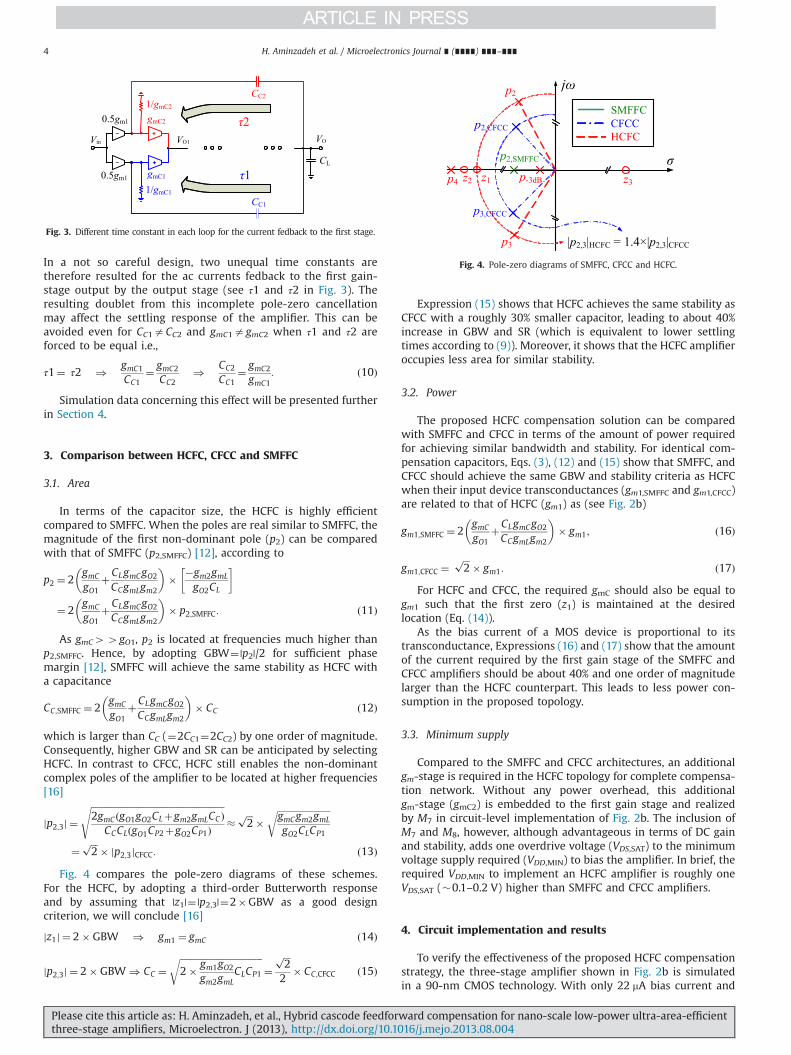
In a not so careful design, two unequal time constants aretherefore resulted for the ac currents fedback to the first gain-stage output by the output stage (see τ1 and τ2 in Fig. 3). Theresulting doublet from this incomplete pole-zero cancellationmay affect the settling response of the amplifier. This can beavoided even for CC1aCC2 and gmC1agmC2 when τ1 and τ2 areforced to be equal i.e.,
τ1¼ τ2 ) gmC1
CC1¼ gmC2
CC2) CC2
CC1¼ gmC2
gmC1: ð10Þ
Simulation data concerning this effect will be presented furtherin Section 4.
3. Comparison between HCFC, CFCC and SMFFC
3.1. Area
In terms of the capacitor size, the HCFC is highly efficientcompared to SMFFC. When the poles are real similar to SMFFC, themagnitude of the first non-dominant pole (p2) can be comparedwith that of SMFFC (p2,SMFFC) [12], according to
p2 ¼ 2gmC
gO1þCL
CC
gmCgO2gmLgm2
� �gm2gmL
gO2CL
� �
¼ 2gmC
gO1þCL
CC
gmCgO2gmLgm2
� p2;SMFFC: ð11Þ
As gmC44gO1, p2 is located at frequencies much higher thanp2,SMFFC. Hence, by adopting GBW¼ |p2|/2 for sufficient phasemargin [12], SMFFC will achieve the same stability as HCFC witha capacitance
CC;SMFFC ¼ 2gmC
gO1þCL
CC
gmCgO2gmLgm2
� CC ð12Þ
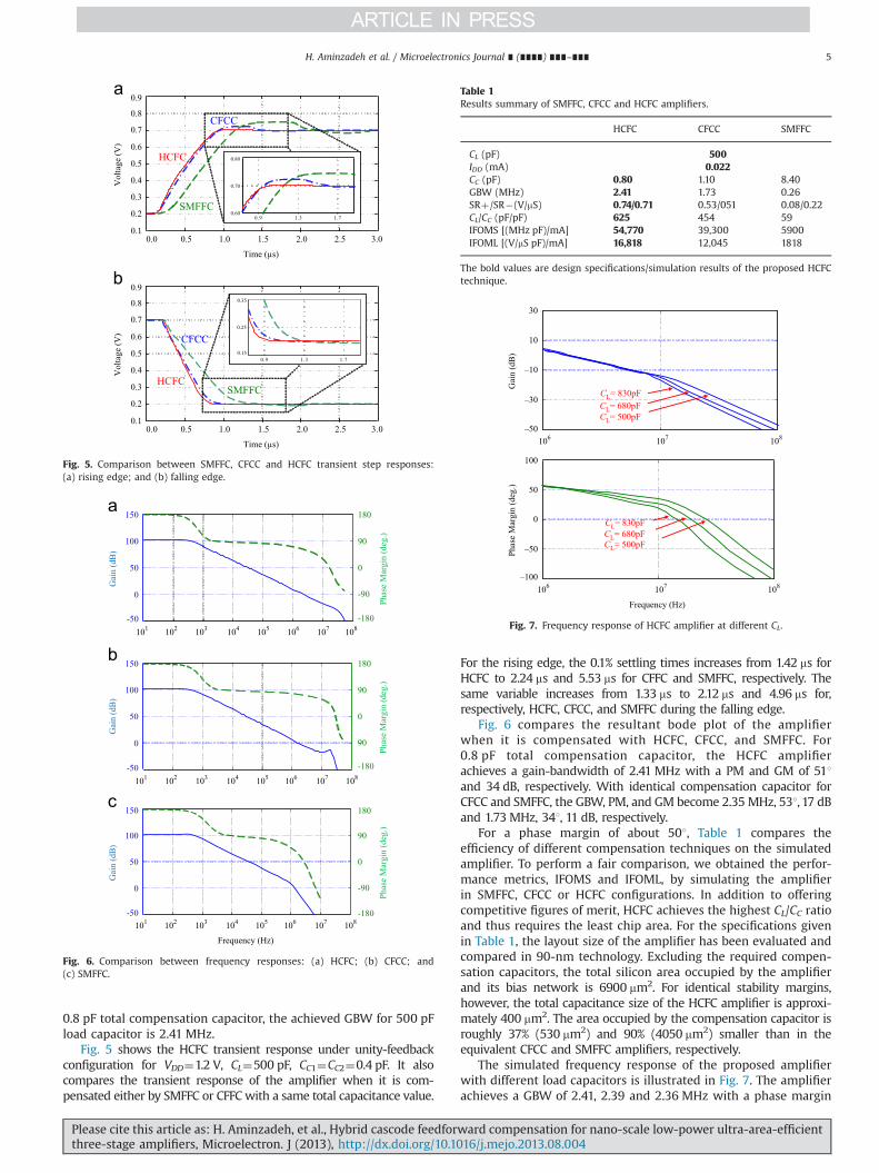
which is larger than CC (¼2CC1¼2CC2) by one order of magnitude.Consequently, higher GBW and SR can be anticipated by selectingHCFC. In contrast to CFCC, HCFC still enables the non-dominantcomplex poles of the amplifier to be located at higher frequencies[16]
jp2;3j ¼ffiffiffiffiffiffiffiffiffiffiffiffiffiffiffiffiffiffiffiffiffiffiffiffiffiffiffiffiffiffiffiffiffiffiffiffiffiffiffiffiffiffiffiffiffiffiffiffiffiffiffiffiffiffiffiffiffiffi2gmC ðgO1gO2CLþgm2gmLCCÞ
CCCLðgO1CP2þgO2CP1Þ
s�
ffiffiffi2
p�
ffiffiffiffiffiffiffiffiffiffiffiffiffiffiffiffiffiffiffiffiffiffiffigmCgm2gmL
gO2CLCP1
r
¼ffiffiffi2
p� jp2;3jCFCC: ð13Þ
Fig. 4 compares the pole-zero diagrams of these schemes.For the HCFC, by adopting a third-order Butterworth responseand by assuming that |z1|¼ |p2,3|¼2�GBW as a good designcriterion, we will conclude [16]
jz1j ¼ 2� GBW ) gm1 ¼ gmC ð14Þ
jp2;3j ¼ 2� GBW ) CC ¼ffiffiffiffiffiffiffiffiffiffiffiffiffiffiffiffiffiffiffiffiffiffiffiffiffiffiffiffiffiffiffiffiffiffiffiffi2� gm1gO2
gm2gmLCLCP1
r¼
ffiffiffi2
p
2� CC;CFCC ð15Þ
Expression (15) shows that HCFC achieves the same stability asCFCC with a roughly 30% smaller capacitor, leading to about 40%increase in GBW and SR (which is equivalent to lower settlingtimes according to (9)). Moreover, it shows that the HCFC amplifieroccupies less area for similar stability.
3.2. Power
The proposed HCFC compensation solution can be comparedwith SMFFC and CFCC in terms of the amount of power requiredfor achieving similar bandwidth and stability. For identical com-pensation capacitors, Eqs. (3), (12) and (15) show that SMFFC, andCFCC should achieve the same GBW and stability criteria as HCFCwhen their input device transconductances (gm1,SMFFC and gm1,CFCC)are related to that of HCFC (gm1) as (see Fig. 2b)
gm1;SMFFC ¼ 2gmC
gO1þCL
CC
gmCgO2gmLgm2
� gm1; ð16Þ
gm1;CFCC ¼ffiffiffi2
p� gm1: ð17Þ
For HCFC and CFCC, the required gmC should also be equal togm1 such that the first zero (z1) is maintained at the desiredlocation (Eq. (14)).
As the bias current of a MOS device is proportional to itstransconductance, Expressions (16) and (17) show that the amountof the current required by the first gain stage of the SMFFC andCFCC amplifiers should be about 40% and one order of magnitudelarger than the HCFC counterpart. This leads to less power con-sumption in the proposed topology.
3.3. Minimum supply
Compared to the SMFFC and CFCC architectures, an additionalgm-stage is required in the HCFC topology for complete compensa-tion network. Without any power overhead, this additionalgm-stage (gmC2) is embedded to the first gain stage and realizedby M7 in circuit-level implementation of Fig. 2b. The inclusion ofM7 and M8, however, although advantageous in terms of DC gainand stability, adds one overdrive voltage (VDS,SAT) to the minimumvoltage supply required (VDD,MIN) to bias the amplifier. In brief, therequired VDD,MIN to implement an HCFC amplifier is roughly oneVDS,SAT (�0.1–0.2 V) higher than SMFFC and CFCC amplifiers.
4. Circuit implementation and results
To verify the effectiveness of the proposed HCFC compensationstrategy, the three-stage amplifier shown in Fig. 2b is simulatedin a 90-nm CMOS technology. With only 22 mA bias current and
Fig. 3. Different time constant in each loop for the current fedback to the first stage.
Fig. 4. Pole-zero diagrams of SMFFC, CFCC and HCFC.
H. Aminzadeh et al. / Microelectronics Journal ∎ (∎∎∎∎) ∎∎∎–∎∎∎4
Please cite this article as: H. Aminzadeh, et al., Hybrid cascode feedforward compensation for nano-scale low-power ultra-area-efficientthree-stage amplifiers, Microelectron. J (2013), http://dx.doi.org/10.1016/j.mejo.2013.08.004i
0.8 pF total compensation capacitor, the achieved GBW for 500 pFload capacitor is 2.41 MHz.
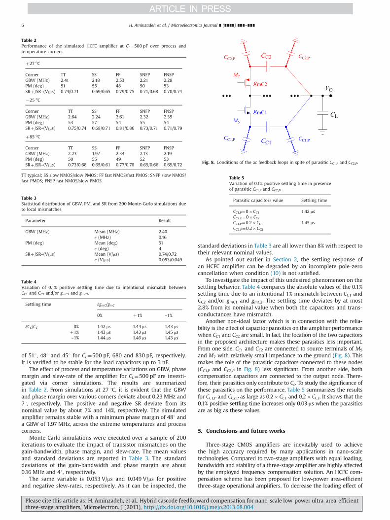
Fig. 5 shows the HCFC transient response under unity-feedbackconfiguration for VDD¼1.2 V, CL¼500 pF, CC1¼CC2¼0.4 pF. It alsocompares the transient response of the amplifier when it is com-pensated either by SMFFC or CFFC with a same total capacitance value.
For the rising edge, the 0.1% settling times increases from 1.42 ms forHCFC to 2.24 ms and 5.53 ms for CFFC and SMFFC, respectively. Thesame variable increases from 1.33 ms to 2.12 ms and 4.96 ms for,respectively, HCFC, CFCC, and SMFFC during the falling edge.
Fig. 6 compares the resultant bode plot of the amplifierwhen it is compensated with HCFC, CFCC, and SMFFC. For0.8 pF total compensation capacitor, the HCFC amplifierachieves a gain-bandwidth of 2.41 MHz with a PM and GM of 511and 34 dB, respectively. With identical compensation capacitor forCFCC and SMFFC, the GBW, PM, and GM become 2.35 MHz, 531, 17 dBand 1.73 MHz, 341, 11 dB, respectively.
For a phase margin of about 501, Table 1 compares theefficiency of different compensation techniques on the simulatedamplifier. To perform a fair comparison, we obtained the perfor-mance metrics, IFOMS and IFOML, by simulating the amplifierin SMFFC, CFCC or HCFC configurations. In addition to offeringcompetitive figures of merit, HCFC achieves the highest CL/CC ratioand thus requires the least chip area. For the specifications givenin Table 1, the layout size of the amplifier has been evaluated andcompared in 90-nm technology. Excluding the required compen-sation capacitors, the total silicon area occupied by the amplifierand its bias network is 6900 mm2. For identical stability margins,however, the total capacitance size of the HCFC amplifier is approxi-mately 400 mm2. The area occupied by the compensation capacitor isroughly 37% (530 mm2) and 90% (4050 mm2) smaller than in theequivalent CFCC and SMFFC amplifiers, respectively.
The simulated frequency response of the proposed amplifierwith different load capacitors is illustrated in Fig. 7. The amplifierachieves a GBW of 2.41, 2.39 and 2.36 MHz with a phase margin
Fig. 5. Comparison between SMFFC, CFCC and HCFC transient step responses:(a) rising edge; and (b) falling edge.
-50
0
50
100
150
-180
-90
0
90
180
Gai
n (d
B)
-50
0
50
100
150
101
-180
-90
0
90
180
102 103 104 105 106 107 108
Gai
n (d
B)
-50
0
50
100
150
101 -180
-90
0
90
180
102 103 104 105 106 107 108
Gai
n (d
B)
Phas
e M
argi
n (d
eg.)
Phas
e M
argi
n (d
eg.)
Frequency (Hz)
Phas
e M
argi
n (d
eg.)
101 102 103 104 105 106 107 108
Fig. 6. Comparison between frequency responses: (a) HCFC; (b) CFCC; and(c) SMFFC.
Table 1Results summary of SMFFC, CFCC and HCFC amplifiers.
HCFC CFCC SMFFC
CL (pF) 500IDD (mA) 0.022CC (pF) 0.80 1.10 8.40GBW (MHz) 2.41 1.73 0.26SRþ/SR�(V/mS) 0.74/0.71 0.53/051 0.08/0.22CL/CC (pF/pF) 625 454 59IFOMS [(MHz pF)/mA] 54,770 39,300 5900IFOML [(V/mS pF)/mA] 16,818 12,045 1818
The bold values are design specifications/simulation results of the proposed HCFCtechnique.
107 108 –100
–50
0
50
100
106
CL= 830pF CL= 680pF CL= 500pF
Frequency (Hz)
Phas
e M
argi
n (d
eg.)
–50
–30
–10
10
30
Gai
n (d
B)
106 107 108
CL= 830pF CL= 680pF CL= 500pF
Fig. 7. Frequency response of HCFC amplifier at different CL.
H. Aminzadeh et al. / Microelectronics Journal ∎ (∎∎∎∎) ∎∎∎–∎∎∎ 5
Please cite this article as: H. Aminzadeh, et al., Hybrid cascode feedforward compensation for nano-scale low-power ultra-area-efficientthree-stage amplifiers, Microelectron. J (2013), http://dx.doi.org/10.1016/j.mejo.2013.08.004i
of 511, 481 and 451 for CL¼500 pF, 680 and 830 pF, respectively.It is verified to be stable for the load capacitors up to 3 nF.
The effect of process and temperature variations on GBW, phasemargin and slew-rate of the amplifier for CL¼500 pF are investi-gated via corner simulations. The results are summarizedin Table 2. From simulations at 27 1C, it is evident that the GBWand phase margin over various corners deviate about 0.23 MHz and71, respectively. The positive and negative SR deviate from itsnominal value by about 7% and 14%, respectively. The simulatedamplifier remains stable with a minimum phase margin of 481 anda GBW of 1.97 MHz, across the extreme temperatures and processcorners.
Monte Carlo simulations were executed over a sample of 200iterations to evaluate the impact of transistor mismatches on thegain-bandwidth, phase margin, and slew-rate. The mean valuesand standard deviations are reported in Table 3. The standarddeviations of the gain-bandwidth and phase margin are about0.16 MHz and 41, respectively.
The same variable is 0.053 V/ms and 0.049 V/ms for positiveand negative slew-rates, respectively. As it can be inspected, the
standard deviations in Table 3 are all lower than 8% with respect totheir relevant nominal values.
As pointed out earlier in Section 2, the settling response ofan HCFC amplifier can be degraded by an incomplete pole-zerocancellation when condition (10) is not satisfied.
To investigate the impact of this undesired phenomenon on thesettling behavior, Table 4 compares the absolute values of the 0.1%settling time due to an intentional 1% mismatch between CC1 andCC2 and/or gmC1 and gmC2. The settling time deviates by at most2.8% from its nominal value when both the capacitors and trans-conductances have mismatch.
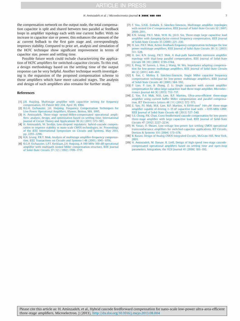
Another non-ideal factor which is in connection with the relia-bility is the effect of capacitor parasitics on the amplifier performancewhen CC1 and CC2 are small. In fact, the location of the two capacitorsin the proposed architecture makes these parasitics less important.From one side, CC1 and CC2 are connected to source terminals of M5
and M7 with relatively small impedance to the ground (Fig. 8). Thismakes the role of the parasitic capacitors connected to these nodes(CC1,P and CC2,P in Fig. 8) less significant. From another side, bothcompensation capacitors are connected to the output node. There-fore, their parasitics only contribute to CL. To study the significance ofthese parasitics on the performance, Table 5 summarizes the resultsfor CC1,P and CC2,P as large as 0.2�CC1 and 0.2�CC2. It shows that the0.1% positive settling time increases only 0.03 ms when the parasiticsare as big as these values.
5. Conclusions and future works
Three-stage CMOS amplifiers are inevitably used to achievethe high accuracy required by many applications in nano-scaletechnologies. Compared to two-stage amplifiers with equal loading,bandwidth and stability of a three-stage amplifier are highly affectedby the employed frequency compensation solution. An HCFC com-pensation scheme has been proposed for low-power area-efficientthree-stage operational amplifiers. To decrease the loading effect of
Table 2Performance of the simulated HCFC amplifier at CL¼500 pF over process andtemperature corners.
þ27 oC
Corner TT SS FF SNFP FNSPGBW (MHz) 2.41 2.18 2.53 2.21 2.29PM (deg) 51 55 48 50 53SRþ/SR–(V/ms) 0.74/0.71 0.69/0.65 0.79/0.75 0.71/0.68 0.70/0.74
�25 oC
Corner TT SS FF SNFP FNSPGBW (MHz) 2.64 2.24 2.61 2.32 2.35PM (deg) 53 57 54 55 54SRþ/SR–(V/ms) 0.75/0.74 0.68/0.71 0.81/0.86 0.73/0.71 0.71/0.79
þ85 oC
Corner TT SS FF SNFP FNSPGBW (MHz) 2.23 1.97 2.34 2.13 2.19PM (deg) 50 55 49 52 53SRþ/SR–(V/ms) 0.73/0.68 0.65/0.61 0.77/0.76 0.69/0.66 0.69/0.72
TT typical; SS slow NMOS/slow PMOS; FF fast NMOS/fast PMOS; SNFP slow NMOS/fast PMOS; FNSP fast NMOS/slow PMOS.
Table 3Statistical distribution of GBW, PM, and SR from 200 Monte-Carlo simulations dueto local mismatches.
Parameter Result
GBW (MHz) Mean (MHz) 2.40s (MHz) 0.16
PM (deg) Mean (deg) 51s (deg) 4
SRþ/SR–(V/ms) Mean (V/ms) 0.74/0.72s (V/ms) 0.053/0.049
Table 4Variation of 0.1% positive settling time due to intentional mismatch betweenCC1 and CC2 and/or gmC1 and gmC2.
Settling time δgmC/gmC
0% þ1% –1%
δCC/CC 0% 1.42 ms 1.44 ms 1.43 msþ1% 1.43 ms 1.43 ms 1.45 ms–1% 1.44 ms 1.46 ms 1.43 ms
Fig. 8. Conditions of the ac feedback loops in spite of parasitic CC1,P and CC2,P.
Table 5Variation of 0.1% positive settling time in presenceof parasitic CC1,P and CC2,P.
Parasitic capacitors value Settling time
CC1,P¼0�CC1 1.42 msCC2,P¼0�CC2CC1,P¼0.2�CC1 1.45 msCC2,P¼0.2�CC2
H. Aminzadeh et al. / Microelectronics Journal ∎ (∎∎∎∎) ∎∎∎–∎∎∎6
Please cite this article as: H. Aminzadeh, et al., Hybrid cascode feedforward compensation for nano-scale low-power ultra-area-efficientthree-stage amplifiers, Microelectron. J (2013), http://dx.doi.org/10.1016/j.mejo.2013.08.004i
the compensation network on the output node, the total compensa-tion capacitor is split and shared between two parallel ac feedbackloops in amplifier topology each with one current buffer. With noincrease in capacitor size or power, this enhances the amount of theac current fedback to the first gain stage and, correspondingly,improves stability. Compared to prior art, analysis and simulation ofthe HCFC technique show significant improvement in terms ofcapacitor size, power and settling time.
Possible future work could include characterizing the applica-tion of HCFC amplifiers for switched-capacitor circuits. To this end,a design methodology based on the settling time of the outputresponse can be very helpful. Another technique worth investigat-ing is the expansion of the proposed compensation scheme tothose amplifiers which have more cascaded stages. The analysisand design of such amplifiers also remains for further study.
References
[1] J.H. Huijsing, Multistage amplifier with capacitive nesting for frequencycompensation, US Patent 602 234, April 19, 1984.
[2] R.G.H. Eschauzier, J.H. Huijsing, Frequency Compensation Techniques forLow-Power Operational Amplifiers, Kluwer, Boston, MA, 1995.
[3] H. Aminzadeh, Three-stage nested-Miller-compensated operational ampli-fiers: analysis, design, and optimization based on settling time, InternationalJournal of Circuit Theory and Applications 39 (6) (2011) 573–587.
[4] H. Aminzadeh, W. Serdijn, Low-dropout regulators: hybrid-cascode compen-sation to improve stability in nano-scale CMOS technologies, in: Proceedingsof the IEEE International Symposium on Circuits and Systems, May 2011,pp. 2293–2296.
[5] K.N. Leung, P.K.T. Mok, Analysis of multistage amplifier-frequency compensa-tion, IEEE Transactions on Circuits and Systems I 48 (2001) 1041–1056.
[6] R.G.H. Eschauzier, L.P.T. Kerklaan, J.H. Huijsing, A 100-MHz 100-dB operationalamplifier with multipath nested Miller compensation structure, IEEE Journalof Solid-State Circuits 27 (12) (1992) 1709–1717.
[7] F. You, S.H.K. Embabi, E. Sánchez-Sinencio, Multistage amplifier topologieswith nested Gm-C compensation, IEEE Journal of Solid-State Circuits 32 (1997)2000–2011.
[8] K.N. Leung, P.K.T. Mok, W.H. Ki, J.K.O. Sin, Three-stage large capacitive loadamplifier with damping-factor-control frequency compensation, IEEE Journalof Solid-State Circuits 35 (2000) 221–230.
[9] H. Lee, P.K.T. Mok, Active-feedback frequency compensation technique for lowpower multistage amplifiers, IEEE Journal of Solid-State Circuits 38 (3) (2003)511–520.
[10] H. Lee, K.N. Leung, P.K.T. Mok, A dual-path bandwidth extension amplifiertopology with dual-loop parallel compensation, IEEE Journal of Solid-StateCircuits 38 (10) (2003) 1739–1744.
[11] X. Peng, W. Sansen, L. Hou, J. Wang, W. Wu, Impedance adapting compensa-tion for low-power multistage amplifiers, IEEE Journal of Solid-State Circuits46 (2) (2011) 445–451.
[12] X. Fan, C. Mishra, E. Sánchez-Sinencio, Single Miller capacitor frequencycompensation technique for low-power multistage amplifiers, IEEE Journalof Solid-State Circuits 40 (2005) 584–592.
[13] P. Liao, P. Luo, B. Zhang, Z. Li, Single capacitor with current amplifiercompensation for ultra-large capacitive load three-stage amplifier, Microelec-tronics Journal 44 (8) (2013) 712–717.
[14] Z. Yan, P.-I. Mak, M.K. Law, R.P. Martins, Ultra-area-efficient three-stageamplifier using current buffer Miller compensation and parallel compensa-tion, IET Electronics Letters 48 (11) (2012) 572–573.
[15] Z. Yan, P.I. Mak, M.K. Law, R.P. Martins, A 0.016-mm2 144-mW three-stageamplifier capable of driving 1–15 nF capacitive load with 40.95-MHz GBW,IEEE Journal of Solid-State Circuits 48 (2013) 527–540.
[16] S.S. Chong, P.K. Chan, Cross feedforward cascode compensation for low-powerthree-stage amplifier with large capacitive load, IEEE Journal of Solid-StateCircuits 47 (2012) 2227–2234.
[17] M. Yavari, O. Shoaei, Low-voltage low-power fast settling CMOS operationaltransconductance amplifiers for switched-capacitor applications, IET Circuits,Devices & Systems 151 (2004) 573–578.
[18] B. Razavi, Design of Analog CMOS Integrated Circuits, McGraw-Hill, New York,2001.
[19] H. Aminzadeh, M. Danaie, R. Lotfi, Design of high-speed two-stage cascode-compensated operational amplifiers based on settling time and open-loopparameters, Integration, the VLSI Journal 41 (2008) 183–192.
H. Aminzadeh et al. / Microelectronics Journal ∎ (∎∎∎∎) ∎∎∎–∎∎∎ 7
Please cite this article as: H. Aminzadeh, et al., Hybrid cascode feedforward compensation for nano-scale low-power ultra-area-efficientthree-stage amplifiers, Microelectron. J (2013), http://dx.doi.org/10.1016/j.mejo.2013.08.004i
Related Documents