ISSN:1369 7021 © Elsevier Ltd 2011 SEPTEMBER 2011 | VOLUME 14 | NUMBER 9 398 The technological trend in large-area electronics including displays, sensors, and actuators is that the form is thin and lightweight. This trend is currently undergoing further developments to make electronics that are also bendable and rollable, i.e., flexible electronics. In fact, flexibility is required for larger electronics to realize the simultaneous achievement of portability and mechanical robustness. Utilizing various types of flexible TFTs 1-5 , a number of flexible applications on plastic have been demonstrated, such as solar cells 6 , light emitting diodes 7 , thin-film transistors 8 , memory devices 9-13 , sensors 14 , actuators 15 , displays 16 , and transponders 17 ; however, mechanical flexibility has not been frequently evaluated. Although the mechanical flexibility of amorphous-silicone 3 and organic transistors 4 on plastic have been reported, the operation voltages are higher than 40 V. This is because of the rough surface of the plastic films (typically 2 – 3 nm more in RMS), which requires thick polymeric gate dielectric layers. Recently, high-capacitive gate dielectric materials have been developed to reduce the operation voltage of organic transistors. In particular, Marks et al. reported self-assembled nanometer-thick dielectrics that achieved an operation voltage of 3 V 18 . Bao et al. reported a 10 nm thick PVP dielectric layer that achieved 2 V operation 19 . However, the use of these materials on glass or rigid substrates has been limited thus far 18-21 . Essentially, it is very difficult to manufacture dielectric layers with single-nanometer-thick gates and high performance transistors on plastic because of its intrinsic surface roughness. One promising approach towards the fabrication of ultraflexible circuits with high electrical performances is micro-contact printing (such as material transfer methods) that can transfer TFT circuits from rigid to flexible and stretchable substrates after circuit fabrication 1,22-26 . Rogers et al. reported very high-performance inorganic-based TFT circuits on rubber substrates utilizing a photolithographic process and Many electronic systems such as flat-panel displays, optical detectors, and sensor arrays would benefit greatly from mechanical flexibility. Ultraflexible and foldable electronics demonstrate ultimate flexibility, and are highly portable. A major obstacle toward the development of foldable electronics is the fundamental compromise between operation voltage, transistor performance, and mechanical flexibility. This review describes foldable and conformable integrated circuits based on organic thin-film transistors (TFTs) with very high mechanical stability. We review our work on such transistors and integrated circuits, that continue to operate without failure, without detectable degradation during folding of the plastic substrate. Tsuyoshi Sekitani* and Takao Someya Department of Electrical Engineering and Information Systems, School of Engineering, The University of Tokyo, Japan *E-mail: [email protected] Human-friendly organic integrated circuits

Welcome message from author
This document is posted to help you gain knowledge. Please leave a comment to let me know what you think about it! Share it to your friends and learn new things together.
Transcript

ISSN:1369 7021 © Elsevier Ltd 2011SEPTEMBER 2011 | VOLUME 14 | NUMBER 9398
The technological trend in large-area electronics including displays,
sensors, and actuators is that the form is thin and lightweight.
This trend is currently undergoing further developments to
make electronics that are also bendable and rollable, i.e., flexible
electronics. In fact, flexibility is required for larger electronics to
realize the simultaneous achievement of portability and mechanical
robustness. Utilizing various types of flexible TFTs1-5, a number of
flexible applications on plastic have been demonstrated, such as
solar cells6, light emitting diodes7, thin-film transistors8, memory
devices9-13, sensors14, actuators15, displays16, and transponders17;
however, mechanical flexibility has not been frequently evaluated.
Although the mechanical flexibility of amorphous-silicone3 and
organic transistors4 on plastic have been reported, the operation
voltages are higher than 40 V. This is because of the rough surface
of the plastic films (typically 2 – 3 nm more in RMS), which
requires thick polymeric gate dielectric layers.
Recently, high-capacitive gate dielectric materials have been
developed to reduce the operation voltage of organic transistors.
In particular, Marks et al. reported self-assembled nanometer-thick
dielectrics that achieved an operation voltage of 3 V18. Bao et al.
reported a 10 nm thick PVP dielectric layer that achieved 2 V
operation19. However, the use of these materials on glass or rigid
substrates has been limited thus far18-21. Essentially, it is very difficult
to manufacture dielectric layers with single-nanometer-thick gates and
high performance transistors on plastic because of its intrinsic surface
roughness.
One promising approach towards the fabrication of ultraflexible
circuits with high electrical performances is micro-contact printing (such
as material transfer methods) that can transfer TFT circuits from rigid
to flexible and stretchable substrates after circuit fabrication1,22-26.
Rogers et al. reported very high-performance inorganic-based TFT
circuits on rubber substrates utilizing a photolithographic process and
Many electronic systems such as flat-panel displays, optical detectors, and sensor arrays would benefit greatly from mechanical flexibility. Ultraflexible and foldable electronics demonstrate ultimate flexibility, and are highly portable. A major obstacle toward the development of foldable electronics is the fundamental compromise between operation voltage, transistor performance, and mechanical flexibility. This review describes foldable and conformable integrated circuits based on organic thin-film transistors (TFTs) with very high mechanical stability. We review our work on such transistors and integrated circuits, that continue to operate without failure, without detectable degradation during folding of the plastic substrate.
Tsuyoshi Sekitani* and Takao Someya
Department of Electrical Engineering and Information Systems, School of Engineering, The University of Tokyo, Japan
*E-mail: [email protected]
Human-friendly organic integrated circuits
MT149p398_407.indd 398 8/12/2011 11:33:50 AM
Human-friendly organic integrated circuits REVIEW
SEPTEMBER 2011 | VOLUME 14 | NUMBER 9 399
high precision micro-contact printing (so called, soft lithography),
and then, realized flexible OLED lighting, waterproof optics, and
multifunctional balloon catheters for bio-integrated electronics22-25.
Using a similar method, Ma et al. reported the fabrication of single
crystal silicon nanomembrane-based TFTs on a soft plastic substrate,
and demonstrated a record frequency response of 12 GHz. Although
they demonstrated simultaneous achievements of excellent electrical
and mechanical performances using printing, the scalability is limited
because photolithographic processes and inorganic materials were used.
Organic material based TFTs have an excellent scalability because
of the low process temperatures, and since organic circuits can be
fabricated directly on large scale plastic substrates using several
printing technologies, such as inkjet and screen printing13,15.
In this review, we demonstrate ultraflexible circuits in the form
of 2 V operation organic transistors and complementary circuits that
continue to operate without degradation while being folded into a
radius of 100 μm5. This exceptional flexibility and bending stability
is provided by a very thin plastic substrate (12.5 μm), an atomically
smooth planarization coating, and a hybrid encapsulation stack that
places the transistors in a neutral strain position, because Young's
modules of the bottom layer is the same as the top layer.
Device structure and fabricationA complementary electronic circuit (subsequently referred to as
CMOS) is an integrated circuit structure comprising p- and n-type
transistors that complement each other. In conventional inorganic
CMOSs employed in nearly all electronics, the dielectric is a silicon
dioxide layer, several nanometers thick; the semiconductors consist
of p- and n-type silicon, which can be modulated by doping with
accepters or donors. Conventionally, these inorganic CMOSs have been
predominantly fabricated by a photolithographic patterning process on
rigid substrates using high temperature and high energy manufacturing
methods. Owing to the miniaturization from photolithography, the
state of the art resolution of CMOSs has achieved a channel length
of 65 nm, allowing CMOSs to work as high definition data storage
devices, central processing units, and so on; however, because of high
temperature and/or high energy manufacturing methods and rigid
substrates, conventional inorganic CMOSs are incompatible with large
area, cost effective processes on plastic.
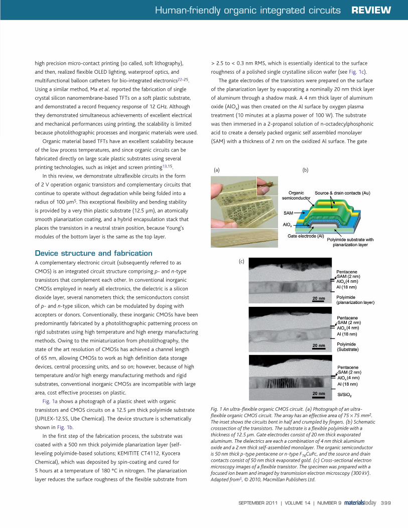
Fig. 1a shows a photograph of a plastic sheet with organic
transistors and CMOS circuits on a 12.5 μm thick polyimide substrate
(UPILEX-12.5S, Ube Chemical). The device structure is schematically
shown in Fig. 1b.
In the first step of the fabrication process, the substrate was
coated with a 500 nm thick polyimide planarization layer (self-
leveling polyimide-based solutions; KEMITITE CT4112, Kyocera
Chemical), which was deposited by spin-coating and cured for
5 hours at a temperature of 180 °C in nitrogen. The planarization
layer reduces the surface roughness of the flexible substrate from
> 2.5 to < 0.3 nm RMS, which is essentially identical to the surface
roughness of a polished single crystalline silicon wafer (see Fig. 1c).
The gate electrodes of the transistors were prepared on the surface
of the planarization layer by evaporating a nominally 20 nm thick layer
of aluminum through a shadow mask. A 4 nm thick layer of aluminum
oxide (AlOx) was then created on the Al surface by oxygen plasma
treatment (10 minutes at a plasma power of 100 W). The substrate
was then immersed in a 2-propanol solution of n-octadecylphosphonic
acid to create a densely packed organic self assembled monolayer
(SAM) with a thickness of 2 nm on the oxidized Al surface. The gate
Fig. 1 An ultra-flexible organic CMOS circuit. (a) Photograph of an ultra-flexible organic CMOS circuit. The array has an effective area of 75 × 75 mm2. The inset shows the circuits bent in half and crumpled by fingers. (b) Schematic crosssection of the transistors. The substrate is a flexible polyimide with a thickness of 12.5 μm. Gate electrodes consist of 20 nm thick evaporated aluminum. The dielectrics are each a combination of 4 nm thick aluminum oxide and a 2 nm thick self-assembled monolayer. The organic semiconductor is 50 nm thick p-type pentacene or n-type F16CuPc, and the source and drain contacts consist of 50 nm thick evaporated gold. (c) Cross-sectional electron microscopy images of a flexible transistor. The specimen was prepared with a focused ion beam and imaged by transmission electron microscopy (300 kV). Adapted from5, © 2010, Macmillan Publishers Ltd.
(a) (b)
(c)
MT149p398_407.indd 399 8/12/2011 11:33:53 AM

REVIEW Human-friendly organic integrated circuits
SEPTEMBER 2011 | VOLUME 14 | NUMBER 9400
dielectric layer is therefore 6 nm thick in total, and has a capacitance
per unit area of 0.6 – 0.65 μF/cm2 27,28.
Fifty nanometer thick layers of the organic semiconductors
pentacene (for p-channel TFTs) and F16CuPc (for n-channel TFTs)
were then deposited by vacuum sublimation through shadow masks.
The source and drain contacts were prepared on top of the organic
semiconductors by evaporating gold Au to a thickness of 50 nm.
Finally, a polymer/metal encapsulation stack (300 nm thick parylene,
200 nm thick gold, and 12.5 μm thick parylene) was deposited to
protect the transistors from air-induced degradation. Consequently,
all measurements reported below were carried out in ambient air.
Furthermore, the deposition of the 13 μm thick encapsulation stack
places the TFTs and circuits at a neutral strain position because Young's
modulus of the bottom layer is the just same as that of the top layer.
Fig. 1c shows a cross-sectional electron microscopy image of a
completed device. The specimen was prepared by using a focused
ion beam and imaged by transmission electron microscopy. The gate
electrode and the two dielectric layers (AlOx and SAM) can clearly be
distinguished in the TEM image. It should be noted that the 2 nm thick
organic SAM and 4 nm thick aluminum oxide layer are clearly resolved
and atomically flat. Owing to a spin-coated planarization-polymer
layer, the TEM image shows the surface smoothness of the SAM and
the quality of the organic/inorganic interfaces.
Transistor performanceThe transistors exhibit excellent electrical performance, as shown
in Figs. 2a – d. A p-type pentacene transistor exhibits a fieldeffect
mobility of 0.5 cm2/Vs and an on/off ratio of > 105, whereas an
n-type F16CuPc transistor exhibits a fieldeffect mobility of 0.01 cm2/
Vs and an on/off ratio of > 104. These characteristics are comparable
to those of devices on glass27. The electrical characteristics are stable
during long term exposure to air for six months. This stability in air is
due to the excellent gas barrier characteristics of the organic/metal
passivation layer29.
By combining a p-type pentacene transistor with an n-type F16CuPc
transistor, a complementary inverter circuit is constructed. This
inverter can operate within 2 V with a gain of more than 65, indicating
excellent inverter performances in 2 V operation (Figs. 2e and f).
In order to evaluate the electrical characteristics under bending
stress, bending experiments are performed on the pentacene transistors
where the direction of source-drain current paths is precisely arranged
parallel and perpendicular to the direction of strain (Fig. 3a). A
capacitor is simultaneously manufactured on the same film, and
its capacitance is measured by varying the bending radius of the
base films (R) in order to obtain the precise capacitance of the gate
dielectric layers as a function of the bending stress. Furthermore, its
capacitor characteristics can function as a strain gauge30. We measured
the electrical properties of the transistors under various inward bending
strains whose magnitudes were systematically controlled by changing
R. Schematic illustrations of inward bending are shown in Fig. 3a.
Fig. 3b shows a micrograph of an organic transistor bent to a radius
of 0.15 mm. Detailed explanations including the experimental setup
and analysis methods of strain evaluated from R are provided in our
previous report30.
Fig. 3c shows source-drain currents (IDS) as a function of R where
IDS is normalized by measurements before the bending experiment.
Pentacene transistors placed at a neutral strain position (manufactured
on a 13 μm thick plastic substrate with encapsulation layers)
exhibit no changes in IDS and can be bent down to about 0.2 mm
without mechanical or electrical damage. For comparison, pentacene
transistors on a 75 μm thick plastic substrate characterized in the
same experiments also exhibit a decrease in IDS from 4 mm. Fig.
3c shows leakage currents (IGS) as a function of R. IGS significantly
increases at bending radii where the decrease in IDS begins. This result
suggests that IDS degradation is mainly due to the destruction of gate
dielectric layers. Through these bending experiments, we confirmed
that organic transistors at neutral strain positions can be bent to
0.2 mm, which is the smallest critical bending radius for transistors
reported thus far.
In our previous reports4,30, we suggested that the effective strains
at the channel layer could be reduced by thinning the base films and
creating a sandwich structure between the sealant and the base film;
quantitative analysis was also shown in a similar structure. When
transistors lack encapsulation layers, inward bending of the base film
induces compressive strains at channel positions and outward tensile
strains. Such strain-induced changes in transistor performance can be
understood in the context of a carrier-hopping model in polycrystalline
thin films. On the other hand, encapsulation layers induce opposite
strains at channel positions. Therefore, transistors with encapsulation
layers that have precisely the same thickness as the base films should
not suffer from the bending stress and should show no significant
changes in transistor characteristics.
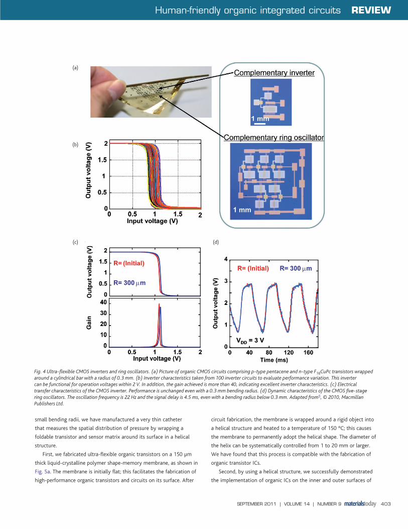
Bending organic complementary (CMOS) circuitsTaking advantage of the ultra-flexible organic transistors with p- and
n-type channels, we manufactured organic CMOS inverters and ring-
oscillators and characterized their performances under very large
bending strains. A photograph of the CMOS circuit at a bending radius
of 0.3 mm is shown in Fig. 4a, along with magnified pictures of the
CMOS inverter and ring oscillator.
Fig. 4b shows the electrical characteristics of 100 CMOS inverters
comprising p-type pentacene and n-type F16CuPc transistors. The
pentacene and F16CuPc transistors have channel widths of 800 and
4400 μm, respectively, and both transistors have a channel length of
20 μm. A difference in channel length is necessary to achieve similar
drain currents for both transistors despite the significant difference
in carrier mobility. The inverter operates with supply voltages
MT149p398_407.indd 400 8/12/2011 11:33:57 AM

Human-friendly organic integrated circuits REVIEW
SEPTEMBER 2011 | VOLUME 14 | NUMBER 9 401
Fig. 2 Static electrical performance of organic transistors on plastic. (a) Drain currents of p-type pentacene transistors as a function of drain-source voltage. Gate-source voltage (VGS) is increased in steps of -0.5 V. (b) Drain and gate currents of pentacene transistors as a function of gate-source voltage where the drain-source voltage (VDS) is −2 V. The observed hysteresis and leakage currents are very small. (c) Drain current of n-type F16CuPc transistors as a function of drain-source voltage. (d) Drain and gate currents of F16CuPc transistors as a function of gate-source voltage where the drain-source voltage (VDS) is −2 V. Owing to the very small thickness of SAM gate dielectrics, the operation voltage is about 2 V. (e, f) Output voltage and gain of a complementary inverter comprising an n-type pentacene TFT and n-type F16CuPc TFTs. Adapted from5, © 2010, Macmillan Publishers Ltd.
(a) (b)
(c) (d)
(e) (f)
MT149p398_407.indd 401 8/12/2011 11:33:57 AM

REVIEW Human-friendly organic integrated circuits
SEPTEMBER 2011 | VOLUME 14 | NUMBER 9402
between 1 and 2 V and a small signal gain of > 40. The variation in
inversion voltages is less than 14 %, indicating excellent performance
consistency. Furthermore, the inverter can function even when
wrapped into a cylindrical bar with a 0.3 mm bending radius, as shown
in Fig. 4c.
A photograph and the electrical transfer characteristics of a five-
stage ring oscillator are shown in Fig. 4. The oscillation frequency
is 22 Hz, and the signal delay is 4.5 ms, which is the fastest among
flexible organic CMOS circuits with a 2 V operating voltage.
Furthermore, the frequency does not change even under a bending
stress of 0.3 mm.
Flexible organic circuits for practical applicationsTo demonstrate a potential electronic application that requires
the operation of high-performance circuits folded into extremely
Fig. 3 Bending experiments of organic transistors on plastic. (a) Photograph of the custom-built bending apparatus in action. Magnified pictures show a capacitor and organic transistors with geometry of applied current parallel and perpendicular to the direction of strain, respectively. The channel length and width of pentacene transistors are 50 and 500 μm, respectively. Devices are stressed using a stress apparatus with a precision mechanical stage4,24. (b) The exact bending radius was determined from digital photographs taken along the bending axis. (c) Drain-source currenta (IDS) as a function of inward bending radius where IDS is normalized by the current before bending. Bending experiments were performed on pentacene transistors located at a neutral strain position (manufactured on 12.5 μm thick plastic and encapsulated by 12.5 μm thick parylene). Red and black lines represent IDS from current parallel and perpendicular to the direction of strain, respectively. The inset shows a magnified view around 0 mm in bending radius. Pentacene transistors located at a neutral strain position can be bent down to 0.2 mm without mechanical and electrical damages. (d) Gate-source currents (IGS) as a function of bending radius. The inset shows a magnified view. IGS (leakage current) significantly increases at bending radii where IDS starts to decrease. Adapted from5, © 2010, Macmillan Publishers Ltd.
(a) (b)
(c) (d)
MT149p398_407.indd 402 8/12/2011 11:33:59 AM
Human-friendly organic integrated circuits REVIEW
SEPTEMBER 2011 | VOLUME 14 | NUMBER 9 403
small bending radii, we have manufactured a very thin catheter
that measures the spatial distribution of pressure by wrapping a
foldable transistor and sensor matrix around its surface in a helical
structure.
First, we fabricated ultra-flexible organic transistors on a 150 μm
thick liquid-crystalline polymer shape-memory membrane, as shown in
Fig. 5a. The membrane is initially flat; this facilitates the fabrication of
high-performance organic transistors and circuits on its surface. After
circuit fabrication, the membrane is wrapped around a rigid object into
a helical structure and heated to a temperature of 150 °C; this causes
the membrane to permanently adopt the helical shape. The diameter of
the helix can be systematically controlled from 1 to 20 mm or larger.
We have found that this process is compatible with the fabrication of
organic transistor ICs.
Second, by using a helical structure, we successfully demonstrated
the implementation of organic ICs on the inner and outer surfaces of
Fig. 4 Ultra-flexible CMOS inverters and ring oscillators. (a) Picture of organic CMOS circuits comprising p-type pentacene and n-type F16CuPc transistors wrapped around a cylindrical bar with a radius of 0.3 mm. (b) Inverter characteristics taken from 100 inverter circuits to evaluate performance variation. This inverter can be functional for operation voltages within 2 V. In addition, the gain achieved is more than 40, indicating excellent inverter characteristics. (c) Electrical transfer characteristics of the CMOS inverter. Performance is unchanged even with a 0.3 mm bending radius. (d) Dynamic characteristics of the CMOS five-stage ring oscillators. The oscillation frequency is 22 Hz and the signal delay is 4.5 ms, even with a bending radius below 0.3 mm. Adapted from5, © 2010, Macmillan Publishers Ltd.
(a)
(b)
(c) (d)
MT149p398_407.indd 403 8/12/2011 11:34:01 AM

REVIEW Human-friendly organic integrated circuits
SEPTEMBER 2011 | VOLUME 14 | NUMBER 9404
ultrafine rubber tubes with a diameter of 1 mm. Owing to its novel
helical structure and great flexibility, the electrically functionalized
tube can bend around turns or corners and hence be wrapped, just
like a tube without transistors. In fact, to demonstrate a possible
application for organic TFTs that operate in the bent state, we
manufactured a thin catheter that measures the spatial distribution
of mechanical pressure. The sensor was fabricated by laminating three
sheets: a foldable 4 × 36 array of pentacene TFTs, a pressure-sensitive
rubber sheet, and a 12.5 μm thick polyimide sheet with a gold
counter electrode. The picture is shown in Fig. 5. The source contacts
Fig. 5 Tightly wound transistor helix. (a) Photograph of a tightly wound transistor active-matrix array in the shape of a tightly wound helix. A TFT array fabricated on a shape-memory polymer film (Nippon Mektron, Ltd.) and permanently transformed into a helix. (b) Transfer curves of individual transistors with and without 80 % stretching. (c) An ultra-flexible active-matrix pressure sensor array as a concept of a catheter that measures the spatial distribution of pressure along its length and circumference by means of an active-matrix sensor helix. (d) Circuit diagram of the pressure sensor cell. The array was fabricated by laminating three sheets: (1) a foldable 4 × 36 array of pentacene TFTs, (2) a pressure-sensitive rubber sheet, and (3) a 12.5 μm thick polyimide sheet with an Au counter electrode. (e) Transfer characteristics of an individual sensor cell measured at two different pressures. (Note that applying pressure to the pressure-sensitive rubber sheet creates a conducting path between the source of the TFT and the counter electrode. Thus, a potential of −3 V is present on the source of the TFT only when pressure is applied, allowing the array to measure the spatial distribution of pressure.) Adapted from5, © 2010, Macmillan Publishers Ltd.
(a) (b)
(c)
(d) (e)
MT149p398_407.indd 404 8/12/2011 11:34:03 AM

Human-friendly organic integrated circuits REVIEW
SEPTEMBER 2011 | VOLUME 14 | NUMBER 9 405
of all 144 transistors are connected to the rubber sheet, whereas
the counter electrode is in contact with the opposite surface of the
rubber sheet. When mechanical pressure is exerted on the catheter,
the electrical resistance between the top and bottom surfaces of
the rubber decreases. A potential of −3 V applied to the counter
electrode is supplied to the TFTs in those positions where pressure is
applied, and thus the spatial distribution of pressure can be obtained
by interrogating the TFTs in the active-matrix array. We believe that
this approach will lead to various kinds of new applications ranging
from functionalization of catheters to artificial blood tubes with
pressure sensors. To show the feasibility of the new concept, we also
demonstrated the measurement of mechanical pressure using the
organic-transistor-based pressure sensors in this configuration.
Organic TFTs with a SAM gate dielectric layer are fabricated not only
on plastics but also on fibers31 and paper32-34. Klauk et al. have fabricated
high-performance organic transistors and circuits on banknotes owing to
very low-temperature processes for TFT fabrication35. Fig. 6 shows organic
circuits on €5 banknotes and a cross-sectional TEM image. The p-type
DNTT TFTs exhibit a mobility of 0.2 cm2/Vs, whereas the n-type F16CuPc
TFTs exhibit a mobility of 0.005 cm2/Vs, which is within five times that of
F16CuPc TFTs on glass27. These circuits can realize anti-counterfeiting and
tracking features in future banknotes.
DiscussionWe have demonstrated the first transistors that operate while folded
into an extremely small bending radius of 100 μm, and the first
integrated circuits that continue to operate without any change in
performance while folded into a radius of 300 μm. Although there are
many previous reports of flexible organic and inorganic transistors,
the transistors in all of these studies were degraded or destroyed
when bent into a radius smaller than a few millimeters, because of
damage by the bend-induced mechanical strain. Although transistors
that survive bending to a radius of 500 μm have been reported by
the Princeton University group9, they require relatively high operating
voltages (15 V), have not been tested during bending (only before
and after); and have not been incorporated into flexible circuits.
To simultaneously achieve extreme bending stability (100 μm) and
low-voltage operation (2 V), we fabricated high-performance organic
Fig. 6 Organic circuits on banknotes. (a) Picture of organic transistors fabricated on a €5 note. (b) Magnified picture of an individual transistor on a banknote. (c) Performances of 92 organic transistors on banknotes, indicating excellent uniformity. Adapted from figure reproduced from35 with permission from Wiley-VCH. © 2011.
(a) (b)
(c)
MT149p398_407.indd 405 8/12/2011 11:34:06 AM

REVIEW Human-friendly organic integrated circuits
SEPTEMBER 2011 | VOLUME 14 | NUMBER 9406
transistors and circuits on a very thin plastic substrate (12.5 μm thick),
dramatically reduced the substrate’s surface roughness with a 500 nm
thick planarization layer that provided an almost atomically smooth
surface, and employed a very thin gate dielectric based on an organic
SEM. Ultimately, we deposited a 13 μm thick encapsulation layer that
not only protects the devices from oxygen and humidity, but places
the transistors in a neutral strain position where the bending-induced
compressive and tensile strains cancel each other out. The current-
voltage characteristics of the organic transistors and circuits do not
change while they are folded into a radius as small as 100 μm.
Although the surface smoothness at channels is crucial for
achieving high-performance transistors and CMOS circuits, almost all
Fig. 7 Future concept of human-friendly organic circuits. (a) Schematic illustration of ultra-flexible large-area electronics that spread over arbitrary curved surfaces and movable parts. (b) Schematic illustration of ultraflexible sensors and lighting for medical applications. Medical sensing and treatments can be performed in blood vessels and unconventional surfaces in the human body.
(a)
(b)
MT149p398_407.indd 406 8/12/2011 11:34:09 AM

Human-friendly organic integrated circuits REVIEW
SEPTEMBER 2011 | VOLUME 14 | NUMBER 9 407
plastics have rough surfaces, leading to poor electrical performance.
In the present work, transistors without the flat-polymer layealso had
very rough interfaces and exhibited a mobility of 0.01 cm2/Vs and
demonstrated large hysteresis. The atomically flat polymer formed a
very smooth surface (0.3 nm in RMS) and gave high-mobility organic
transistors and high-speed organic CMOS circuits.
A SAM gate dielectric is also necessary for simultaneously realizing
foldability (bending radius ~0.3 mm), low-voltage operation (2 V),
and high electrical performance (mobility > 0.5 cm2/Vs on pentacene)
because it enables us to form a very thin and uniform single-
monolayer gate dielectric on plastics without controlling thickness.
Furthermore, the molecules are packed with a sufficient density
(4.6 × 10¹⁴ molecules/cm2) such that SAM could be an ideal ultra-
flexible insulating material.
From the perspective of circuit design, CMOS circuits have
numerous advantages over circuits based on a single carrier type,
including greater noise margin, lower power consumption, and faster
switching speed36. Our foldable organic CMOS can provide new
electronic devices with functionalities that are more resistant to shock.
This will allow users to carry small devices in pockets and fold up large
devices to make them more convenient.
Future prospectsOne of the most attractive features of flexible electronics is their
compatibility with living bodies. In addition to wearable electronics
including sensors and actuators that function from outside the body,
implantable electronics that function inside the body have been
expected to play important roles in safety and securing life, especially
in healthcare. For example, flexible pressure and thermal sensors
could be used to realize electrically powered artificial skin, and flexible
vibration and photo detectors could work as an electrically powered
artificial auris interna and retina, respectively. Given the excellent
mechanical flexibility and softness, users may experience a lower
resistance to electronic objects in their bodies. Furthermore, if the
flexible organic circuits comprise biocompatible materials, electronic
implants could be used in the body without experiencing the rejection
phenomenon.
In addition to healthcare, flexible electronics will be able to expand
into daily life. The flexible organic circuits fabricated onto banknotes
described above could be used as the ultimate anti-counterfeit
technology and tracking system.
Organic integrated circuits with exceptional flexibility and bending
stability will be used to realize new concepts in electronics and
introduce a new era of human-friendly electronic systems.
AcknowledgementsThis study was partially supported by JST/CREST, the GrantinAid for
Scientific Research (KAKENHI; WAKATE S), NEDO, and the Special
Coordination Funds for Promoting and Technology. We thank Hagen
Klauk, Ute Zschieschang (Max Planck Institute for Solid State Research),
Takayasu Sakurai, and Makoto Takamiya (University of Tokyo) for
technical supports, sample preparation, and valuable discussion. We also
thank Athene Co., Ltd for manufacturing very fine shadow masks and
Daisankasei Co., Ltd. for highpurity parylene (diX-SR).
REFERENCES
1. Kodaira, T. et al., J Soc Inf Display (2008) 16/1, 107-111.
2. Nomura, K., et al., Nature (2004) 432, 488.
3. Gleskova, H., et al., J Appl Phys (2002) 92, 6224.
4. Sekitani, T. et al., Appl Phys Lett (2005) 87, 173502.
5. Sekitani, T., et al., Nature Mater (2010) 9, 1015.
6. Ross, R. B. et al., Nature Mater (2009) 8, 208212.
7. Müller, C. D. et al., Nature (2003) 421, 829833.
8. Gelinck, G. H. et al., Nature Mater (2004) 3, 106110.
9. Möller, S., et al., Nature (2003) 426, 166169.
10. Ouyang, J., et al., Nature Mater (2004) 3, 918922.
11. Naber, R. C. G. et al., Nature Mater (2005) 4, 243248.
12. Asadi, K. de Leeuw, et al., Nature Mater (2008) 7, 547550.
13. Sekitani, T. et al., IEEE Trans Electr Dev (2009) 56, 10271035.
14. Someya, T. et al., P Natl Acad Sci USA (2005) 102, 1232112325.
15. Sekitani, T. et al., Nature Mater (2007) 6, 413417.
16. Zhou, L. et al., Appl Phys Lett (2006) 88, 083502.
17. Baude, P. et al., Appl Phys Lett (2003) 82, 39643966.
18. Yoon, M. –H., Facchetti, A., and Marks, T. J. P Natl Acad Sci USA (2005) 102, 4678.
19. Roberts, M. E. et al., P Natl Acad Sci USA (2008) 105, 12134.
20. Ma, H. et al., Appl Phys Lett (2008) 92, 113303.
21. Wöbkenberg, P. H. et al., Appl Phys Lett (2008) 93, 013303.
22. Park., S. et al., Adv Mater (2010) 22, 3062.
23. Kim, R. H. et al., Nature Mater (2010) 9, 929.
24. Kim, D. H. et al., Nature Mater (2010) 9, 511.
25. Kim, D. H. et al., Nature Mater (2011) 10, 316.
26. Sun, L. et al. Small (2010) 6, 2553.
27. Klauk, H., et al., Nature (2007) 445, 745.
28. Sekitani, T., et al., P Natl Acad Sci USA (2008) 105, 49764980.
29. Sekitani, T and Someya, T., Jpn J Appl Phys (2007)46, 43004305.
30. Sekitani, T. et al., Appl Phys Lett (2005) 86, 073511.
31. Lee, J., and Subramanian, V., IEEE T Electron Dev (2005) 52, 269.
32. Andersson, P. et al., Adv Mater (2002) 14, 1460.
33. Eder, F. et al., Appl Phys Lett (2004) 84, 2673.
34. Kim, Y. H., Moon, D. G., and Han, J. I., IEEE Electr Device L (2004) 25, 702.
35. Zschieschang, U. et al., Adv Mater (2011) 23, 654.
36. Crone, B. K. et al., J Appl Phys (2001) 89, 5125.
Instrument citation
Focused ion beam, FB-2100, Hitachi High-Technologies Corp.
Transmission electron microscopy, HF-3300 Cold-FE TEM, 300 kV,
Hitachi High-Technologies Corp.
MT149p398_407.indd 407 8/12/2011 11:34:13 AM
Related Documents


