HTG2150 8-Bit 320 Pixel Dot Matrix LCD MCU Series Rev. 1.30 1 May 21, 2002 Features · Operating voltage: 2.4V~3.6V · 16K´16 bits program ROM · 192´8 bits data RAM · 8~12 bidirectional I/O lines · 8 common´33~40 segment LCD driver · One 16-bit programmable timer with overflow inter- rupts · One 8-bit programmable timer with 8 stage prescaler for PFD · One 8-bit programmable timer with 8 stage prescaler for Time base · One 8-bit PWM audio output to directly drive speaker and buzzer · Watchdog Timer · On-chip RC oscillator for system clock and 32768Hz crystal oscillator for timebase and LCD driver · HALT function and wake-up feature reduce power consumption · 8-level subroutine nesting · Bit manipulation instructions · 63 powerful instructions · One interrupt input · 100-pin QFP package General Description The HTG2150 is an 8-bit high performance RISC-like microcontroller. The single cycle instruction and two-stage pipeline architecture make it suitable for high speed application. The device is ideally suited for multi- ple LCD low power application among which are calcu- lators, clock timer, game, scales, toys and hand held LCD products, as well as for battery systems.

Welcome message from author
This document is posted to help you gain knowledge. Please leave a comment to let me know what you think about it! Share it to your friends and learn new things together.
Transcript
HTG2150
8-Bit 320 Pixel Dot Matrix LCD MCU Series
Rev. 1.30 1 May 21, 2002
Features
� Operating voltage: 2.4V~3.6V
� 16K�16 bits program ROM
� 192�8 bits data RAM
� 8~12 bidirectional I/O lines
� 8 common�33~40 segment LCD driver
� One 16-bit programmable timer with overflow inter-
rupts
� One 8-bit programmable timer with 8 stage prescaler
for PFD
� One 8-bit programmable timer with 8 stage prescaler
for Time base
� One 8-bit PWM audio output to directly drive speaker
and buzzer
� Watchdog Timer
� On-chip RC oscillator for system clock and 32768Hz
crystal oscillator for timebase and LCD driver
� HALT function and wake-up feature reduce power
consumption
� 8-level subroutine nesting
� Bit manipulation instructions
� 63 powerful instructions
� One interrupt input
� 100-pin QFP package
General Description
The HTG2150 is an 8-bit high performance RISC-like
microcontroller. The single cycle instruction and
two-stage pipeline architecture make it suitable for high
speed application. The device is ideally suited for multi-
ple LCD low power application among which are calcu-
lators, clock timer, game, scales, toys and hand held
LCD products, as well as for battery systems.

Block Diagram
HTG2150
Rev. 1.30 2 May 21, 2002
���
� � � � � � �
� � � � � �
� � � � � � �
� � � � � �
� � �
� � � � � � � � � � �
� � � � � � � �
� � � � � � � � � � �
� � � � � � �
� � � � � �
� � � � � � � �
� � � �
� �� � �� � �
� � � � � � � �
� � � � � � �
� � � �
� !
� "���
� � �
� # � #� � � � � $
# % �
� & � ' � � �
� � # � � �
# � �
� � # � ( !
� � # � ( "
� � � !
� � � ! �
� ) � * � % ( � +
" , * - � �� � # � ( .
� � # � ( �
� � # � ( +
� � # � ( /
� � # � ( ,
� � # � ( �
# �
#
� � � * # # ! 0 # �
% � �� � � � � $
% � � * � � � 1 � �
� � � ! 0 � � � �
� � � . �
� � � .
2 �
3 � "
� � � � �
� � � �
� . � , 4 5 6 * � � $ � � � 7
� ! 0 � � . 8 + 0 8 � � � � � 0 � � ,� � � � � � �� � � � � � � 4� � � � � � 9
� ) � * � % (
���
3 � .
8 �
8
� � � * 8 8 + 0 8 � � � � � 0 � � ,
���
� ) � * � % (
4 : � � � � � � � � � � 7 � �
4 : � � � � � � � � � � 7 � �
4 : � � � � � � � � � � 7 � �
3 �
� � # 3 � � # � "
3 � � # � .
� ) � * � % (
3 � � # � "
3 � � # � .
3 � � �
3 � � * � � � � � 7 � �3 � � * � � *� � �� . / ,

Pin Assignment
HTG2150
Rev. 1.30 3 May 21, 2002
"
.
�
+
/
,
�
4
9
" !
" "
" .
" �
" +
" /
" ,
" �
" 4
" 9
. !
. "
. .
. �
. +
. /
. ,
. �
. 4
. 9
� !� " � . � � � + � / � , � � � 4 � 9 + ! + " + . + � + + + / + , + � + 4 + 9 / !
4 "4 .4 �4 +4 /4 ,4 �4 44 99 !9 "9 .9 �9 +9 /9 ,9 �9 49 9" ! !4 !
� 9
� 4
� �
� ,
� /
� +
� �
� .
� "
� !
, 9
, 4
, �
, ,
, /
, +
, �
, .
, "
, !
/ 9
/ 4
/ �
/ ,
/ /
/ +
/ �
/ .
/ "
� �
� �
� �
� �
� �
� �
� �
� �
� . /
� . ,
� . �
� . 4
� . 9
� � !
� � "
� � .
8 + � � � �
8 / � � � +
8 , � � � /
8 � � � � ,
� � � � � � �
� � � � � � � 4
� � � � � � 9
� �
� �
� �
� �
� �
� �
� �
��
��
��
��
#�
#,
#/
#+
#�
#.
#"
#!
���
����
���
3�.
3�"
��
��
��
� �
� �
� �
� �
� �
� �
� �
� 4
� �
� ,
� /
� +
� �
� .
� "
� !
� � � �
� � � ,
� � � /
� � � +
� � � �
� � � .
� � � "
� � � !
� �
� �
� �
� �
� �
� �
��
��
��
�9
�"!
�""
�".
�"�
�"+
�"/
�",
�"�
�"4
�"9
�.!
�."
�..
�.�
�.+
��
� � � � � � �� � � � � � � � �
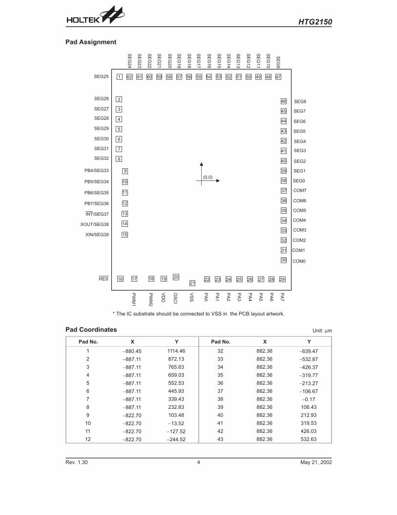
Pad Assignment
* The IC substrate should be connected to VSS in the PCB layout artwork.
Pad Coordinates Unit: �m
Pad No. X Y Pad No. X Y
1 �880.45 1114.46 32 882.36 �639.47
2 �887.11 872.13 33 882.36 �532.87
3 �887.11 765.63 34 882.36 �426.37
4 �887.11 659.03 35 882.36 �319.77
5 �887.11 552.53 36 882.36 �213.27
6 �887.11 445.93 37 882.36 �106.67
7 �887.11 339.43 38 882.36 �0.17
8 �887.11 232.83 39 882.36 106.43
9 �822.70 103.48 40 882.36 212.93
10 �822.70 �13.52 41 882.36 319.53
11 �822.70 �127.52 42 882.36 426.03
12 �822.70 �244.52 43 882.36 532.63
HTG2150
Rev. 1.30 4 May 21, 2002
"
� .
.
� �
�
� +
+
� /
/
� ,
,
� �
�
� 4
4
� 99
+ !
" !
+ "
" "
+ .
" .
+ �
" �
+ +
" +
+ /
" /
+ ,
" ,
+ �
" �
+ 4
" 4
+ 9
" 9
/ !
. !
/ "
. "
/ .
. .
/ �
. �
/ +
. +
/ /
. /
/ ,
. ,
/ �
. �
/ 4
. 4
/ 9
. 9
, !
� !
, "
� "
, .
; ! < ! =
� . /
� . ,
� . �
� . 4
� . 9
� � !
� � "
� � .
8 + � � � �
8 / � � � +
8 , � � � /
8 � � � � ,
� � � � � � � 4
� � � � � � 9
� �
3�"
3�.
���
����
���
#!
#"
#.
#�
#+
#/
#,
#�
� � � !
� � � "
� � � .
� � � �
� � � +
� � � /
� � � ,
� � � �
� �
� .
� "
� !
� +
� �
� ,
� /
� 4
�9
�"!
�""
�".
�"�
�"+
�"/
�",
�"�
�"4
�"9
�.!
�."
�..
�.�
�.+
� � � � � � �
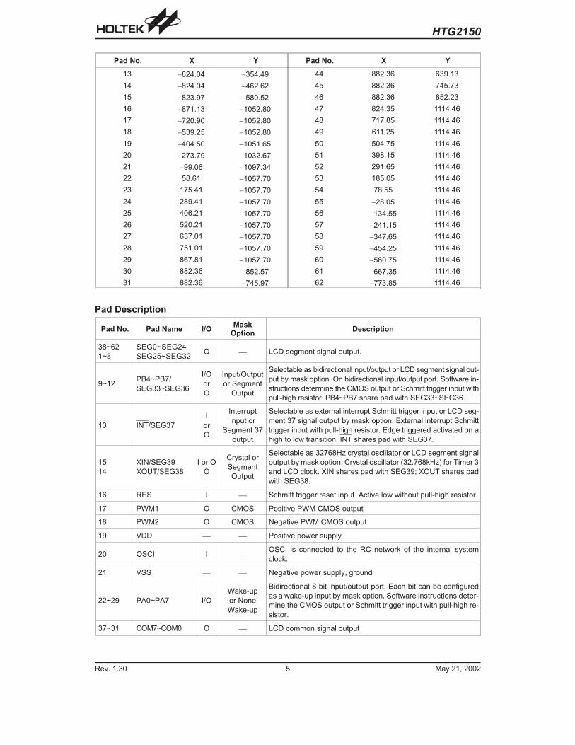
Pad No. X Y Pad No. X Y
13 �824.04 �354.49 44 882.36 639.13
14 �824.04 �462.62 45 882.36 745.73
15 �823.97 �580.52 46 882.36 852.23
16 �871.13 �1052.80 47 824.35 1114.46
17 �720.90 �1052.80 48 717.85 1114.46
18 �539.25 �1052.80 49 611.25 1114.46
19 �404.50 �1051.65 50 504.75 1114.46
20 �273.79 �1032.67 51 398.15 1114.46
21 �99.06 �1097.34 52 291.65 1114.46
22 58.61 �1057.70 53 185.05 1114.46
23 175.41 �1057.70 54 78.55 1114.46
24 289.41 �1057.70 55 �28.05 1114.46
25 406.21 �1057.70 56 �134.55 1114.46
26 520.21 �1057.70 57 �241.15 1114.46
27 637.01 �1057.70 58 �347.65 1114.46
28 751.01 �1057.70 59 �454.25 1114.46
29 867.81 �1057.70 60 �560.75 1114.46
30 882.36 �852.57 61 �667.35 1114.46
31 882.36 �745.97 62 �773.85 1114.46
Pad Description
Pad No. Pad Name I/OMask
OptionDescription
38~62
1~8
SEG0~SEG24
SEG25~SEG32O � LCD segment signal output.
9~12PB4~PB7/
SEG33~SEG36
I/O
or
O
Input/Output
or Segment
Output
Selectable as bidirectional input/output or LCD segment signal out-
put by mask option. On bidirectional input/output port. Software in-
structions determine the CMOS output or Schmitt trigger input with
pull-high resistor. PB4~PB7 share pad with SEG33~SEG36.
13 INT/SEG37
I
or
O
Interrupt
input or
Segment 37
output
Selectable as external interrupt Schmitt trigger input or LCD seg-
ment 37 signal output by mask option. External interrupt Schmitt
trigger input with pull-high resistor. Edge triggered activated on a
high to low transition. INT shares pad with SEG37.
15
14
XIN/SEG39
XOUT/SEG38
I or O
O
Crystal or
Segment
Output
Selectable as 32768Hz crystal oscillator or LCD segment signal
output by mask option. Crystal oscillator (32.768kHz) for Timer 3
and LCD clock. XIN shares pad with SEG39; XOUT shares pad
with SEG38.
16 RES I � Schmitt trigger reset input. Active low without pull-high resistor.
17 PWM1 O CMOS Positive PWM CMOS output
18 PWM2 O CMOS Negative PWM CMOS output
19 VDD � � Positive power supply
20 OSCI I �OSCI is connected to the RC network of the internal system
clock.
21 VSS � � Negative power supply, ground
22~29 PA0~PA7 I/O
Wake-up
or None
Wake-up
Bidirectional 8-bit input/output port. Each bit can be configured
as a wake-up input by mask option. Software instructions deter-
mine the CMOS output or Schmitt trigger input with pull-high re-
sistor.
37~31 COM7~COM0 O � LCD common signal output
HTG2150
Rev. 1.30 5 May 21, 2002
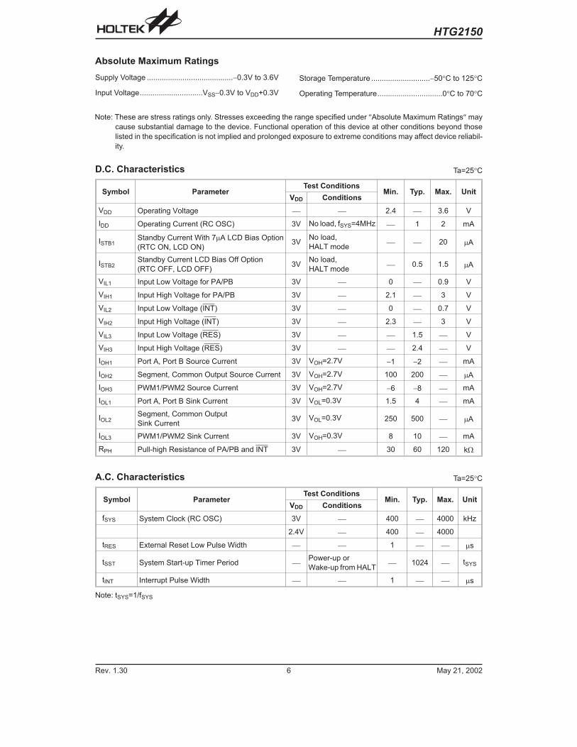
Absolute Maximum Ratings
Supply Voltage .........................................�0.3V to 3.6V Storage Temperature ............................�50�C to 125�C
Input Voltage..............................VSS�0.3V to VDD+0.3V Operating Temperature...............................0�C to 70�C
Note: These are stress ratings only. Stresses exceeding the range specified under �Absolute Maximum Ratings� may
cause substantial damage to the device. Functional operation of this device at other conditions beyond those
listed in the specification is not implied and prolonged exposure to extreme conditions may affect device reliabil-
ity.
D.C. Characteristics Ta=25�C
Symbol ParameterTest Conditions
Min. Typ. Max. UnitVDD Conditions
VDD Operating Voltage � � 2.4 � 3.6 V
IDD Operating Current (RC OSC) 3V No load, fSYS=4MHz � 1 2 mA
ISTB1Standby Current With 7�A LCD Bias Option
(RTC ON, LCD ON)3V
No load,
HALT mode� � 20 �A
ISTB2Standby Current LCD Bias Off Option
(RTC OFF, LCD OFF)3V
No load,
HALT mode� 0.5 1.5 �A
VIL1 Input Low Voltage for PA/PB 3V � 0 � 0.9 V
VIH1 Input High Voltage for PA/PB 3V � 2.1 � 3 V
VIL2 Input Low Voltage (INT) 3V � 0 � 0.7 V
VIH2 Input High Voltage (INT) 3V � 2.3 � 3 V
VIL3 Input Low Voltage (RES) 3V � � 1.5 � V
VIH3 Input High Voltage (RES) 3V � � 2.4 � V
IOH1 Port A, Port B Source Current 3V VOH=2.7V �1 �2 � mA
IOH2 Segment, Common Output Source Current 3V VOH=2.7V 100 200 � �A
IOH3 PWM1/PWM2 Source Current 3V VOH=2.7V �6 �8 � mA
IOL1 Port A, Port B Sink Current 3V VOL=0.3V 1.5 4 � mA
IOL2Segment, Common Output
Sink Current3V VOL=0.3V 250 500 � �A
IOL3 PWM1/PWM2 Sink Current 3V VOH=0.3V 8 10 � mA
RPH Pull-high Resistance of PA/PB and INT 3V � 30 60 120 k�
A.C. Characteristics Ta=25�C
Symbol ParameterTest Conditions
Min. Typ. Max. UnitVDD Conditions
fSYS System Clock (RC OSC) 3V � 400 � 4000 kHz
2.4V � 400 � 4000
tRES External Reset Low Pulse Width � � 1 � � �s
tSST System Start-up Timer Period �Power-up or
Wake-up from HALT� 1024 � tSYS
tINT Interrupt Pulse Width � � 1 � � �s
Note: tSYS=1/fSYS
HTG2150
Rev. 1.30 6 May 21, 2002
HTG2150
Rev. 1.30 7 May 21, 2002
� " � . � � � + � " � . � � � + � " � . � � � +
2 � � � & * � � � � * ; � =
> � � � � � * � � � � * ; � : " = 2 � � � & * � � � � * ; � ? " =
> � � � � � * � � � � * ; � = 2 � � � & * � � � � * ; � ? . =
> � � � � � * � � � � * ; � ? " =
� � ? " � ? .
� $ � � � �� 7 � � @
�
8 � � @ !
8 � � @ "
4 " 9 . � " ,8 � � �
� � � � @
* 8 � � @ * � � � � � �� � � � � � � � * 8 � � / *
� � � * # � � � � � �# " � * - � � * % � � � &
% � � � & * � � � � * � � * > � � � � � � � * � ' * A � � * � � * � � 7 7 * � � � � � � � � � � �" , ( * � � � � � � * � � � * # � � � � � � � � � * # � � & � � � � � � � �
" � * - � � � � � � � � �� � � � � � �
! ! ! ! 5
" 2 2 2 5 . ! ! ! 5
� 2 2 2 5
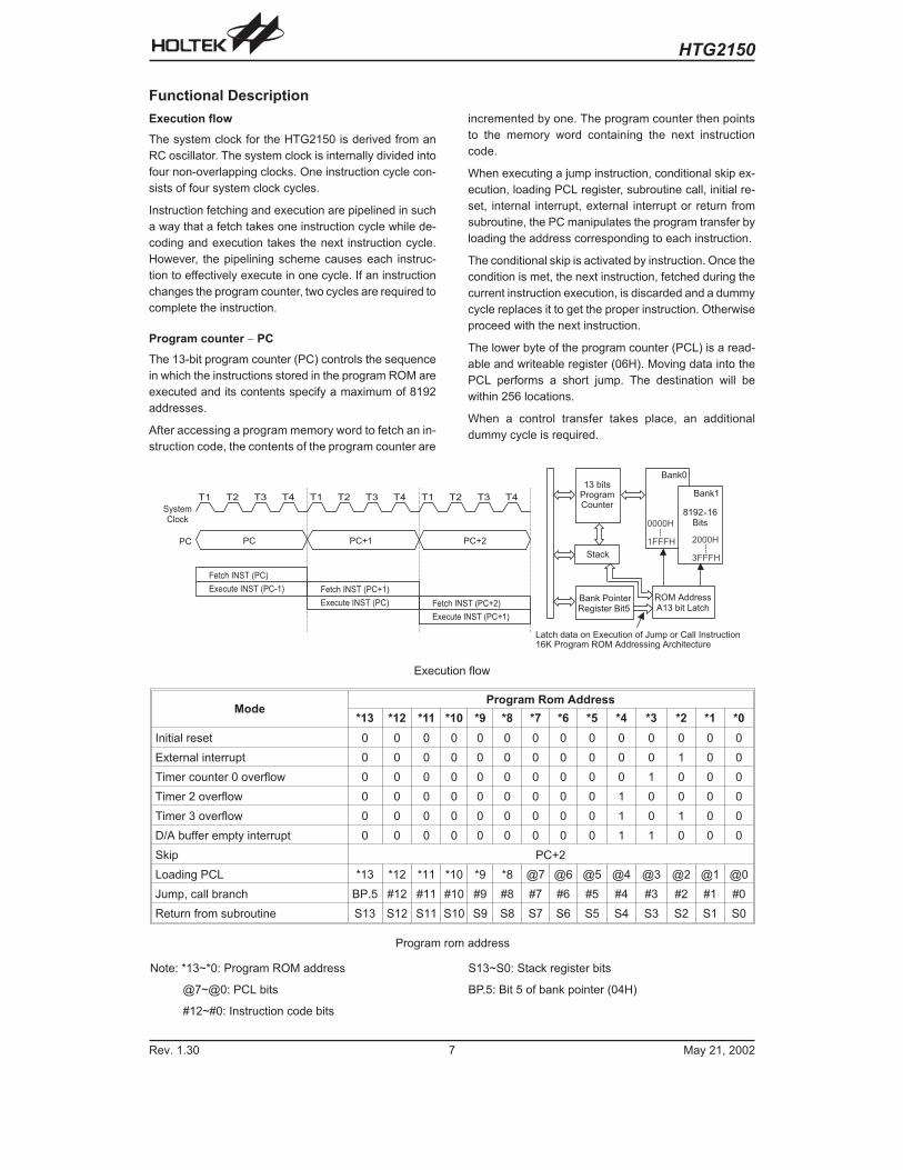
Execution flow
Functional Description
Execution flow
The system clock for the HTG2150 is derived from an
RC oscillator. The system clock is internally divided into
four non-overlapping clocks. One instruction cycle con-
sists of four system clock cycles.
Instruction fetching and execution are pipelined in such
a way that a fetch takes one instruction cycle while de-
coding and execution takes the next instruction cycle.
However, the pipelining scheme causes each instruc-
tion to effectively execute in one cycle. If an instruction
changes the program counter, two cycles are required to
complete the instruction.
Program counter � PC
The 13-bit program counter (PC) controls the sequence
in which the instructions stored in the program ROM are
executed and its contents specify a maximum of 8192
addresses.
After accessing a program memory word to fetch an in-
struction code, the contents of the program counter are
incremented by one. The program counter then points
to the memory word containing the next instruction
code.
When executing a jump instruction, conditional skip ex-
ecution, loading PCL register, subroutine call, initial re-
set, internal interrupt, external interrupt or return from
subroutine, the PC manipulates the program transfer by
loading the address corresponding to each instruction.
The conditional skip is activated by instruction. Once the
condition is met, the next instruction, fetched during the
current instruction execution, is discarded and a dummy
cycle replaces it to get the proper instruction. Otherwise
proceed with the next instruction.
The lower byte of the program counter (PCL) is a read-
able and writeable register (06H). Moving data into the
PCL performs a short jump. The destination will be
within 256 locations.
When a control transfer takes place, an additional
dummy cycle is required.
ModeProgram Rom Address
*13 *12 *11 *10 *9 *8 *7 *6 *5 *4 *3 *2 *1 *0
Initial reset 0 0 0 0 0 0 0 0 0 0 0 0 0 0
External interrupt 0 0 0 0 0 0 0 0 0 0 0 1 0 0
Timer counter 0 overflow 0 0 0 0 0 0 0 0 0 0 1 0 0 0
Timer 2 overflow 0 0 0 0 0 0 0 0 0 1 0 0 0 0
Timer 3 overflow 0 0 0 0 0 0 0 0 0 1 0 1 0 0
D/A buffer empty interrupt 0 0 0 0 0 0 0 0 0 1 1 0 0 0
Skip PC+2
Loading PCL *13 *12 *11 *10 *9 *8 @7 @6 @5 @4 @3 @2 @1 @0
Jump, call branch BP.5 #12 #11 #10 #9 #8 #7 #6 #5 #4 #3 #2 #1 #0
Return from subroutine S13 S12 S11 S10 S9 S8 S7 S6 S5 S4 S3 S2 S1 S0
Program rom address
Note: *13~*0: Program ROM address S13~S0: Stack register bits
@7~@0: PCL bits BP.5: Bit 5 of bank pointer (04H)
#12~#0: Instruction code bits
HTG2150
Rev. 1.30 8 May 21, 2002
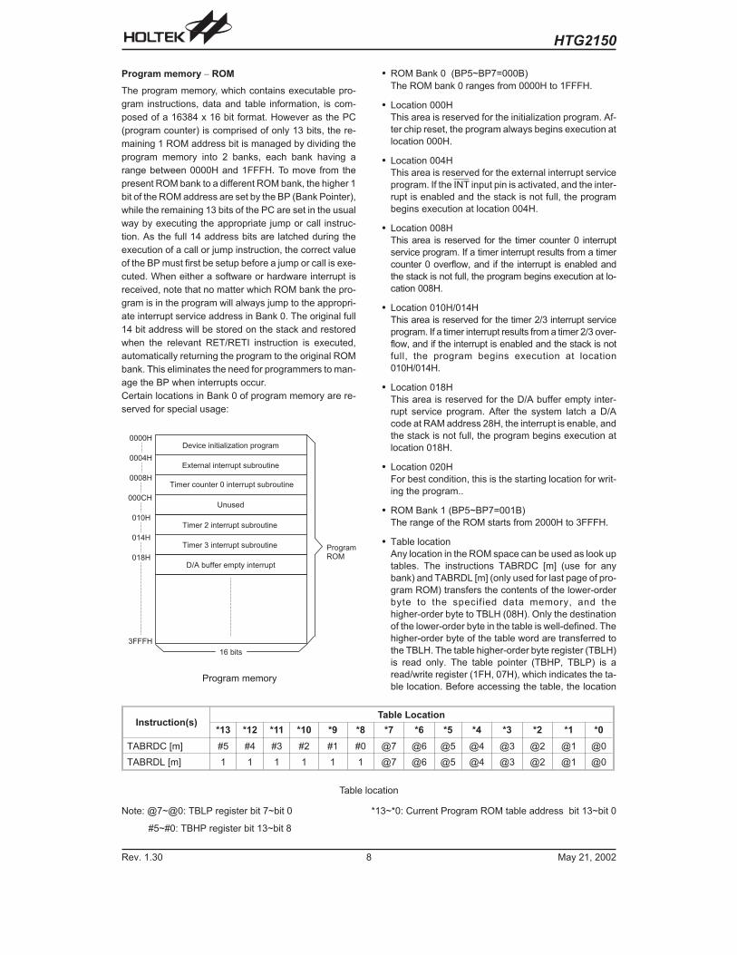
Program memory � ROM
The program memory, which contains executable pro-
gram instructions, data and table information, is com-
posed of a 16384 x 16 bit format. However as the PC
(program counter) is comprised of only 13 bits, the re-
maining 1 ROM address bit is managed by dividing the
program memory into 2 banks, each bank having a
range between 0000H and 1FFFH. To move from the
present ROM bank to a different ROM bank, the higher 1
bit of the ROM address are set by the BP (Bank Pointer),
while the remaining 13 bits of the PC are set in the usual
way by executing the appropriate jump or call instruc-
tion. As the full 14 address bits are latched during the
execution of a call or jump instruction, the correct value
of the BP must first be setup before a jump or call is exe-
cuted. When either a software or hardware interrupt is
received, note that no matter which ROM bank the pro-
gram is in the program will always jump to the appropri-
ate interrupt service address in Bank 0. The original full
14 bit address will be stored on the stack and restored
when the relevant RET/RETI instruction is executed,
automatically returning the program to the original ROM
bank. This eliminates the need for programmers to man-
age the BP when interrupts occur.
Certain locations in Bank 0 of program memory are re-
served for special usage:
� ROM Bank 0 (BP5~BP7=000B)
The ROM bank 0 ranges from 0000H to 1FFFH.
� Location 000H
This area is reserved for the initialization program. Af-
ter chip reset, the program always begins execution at
location 000H.
� Location 004H
This area is reserved for the external interrupt service
program. If the INT input pin is activated, and the inter-
rupt is enabled and the stack is not full, the program
begins execution at location 004H.
� Location 008H
This area is reserved for the timer counter 0 interrupt
service program. If a timer interrupt results from a timer
counter 0 overflow, and if the interrupt is enabled and
the stack is not full, the program begins execution at lo-
cation 008H.
� Location 010H/014H
This area is reserved for the timer 2/3 interrupt service
program. If a timer interrupt results from a timer 2/3 over-
flow, and if the interrupt is enabled and the stack is not
full, the program begins execution at location
010H/014H.
� Location 018H
This area is reserved for the D/A buffer empty inter-
rupt service program. After the system latch a D/A
code at RAM address 28H, the interrupt is enable, and
the stack is not full, the program begins execution at
location 018H.
� Location 020H
For best condition, this is the starting location for writ-
ing the program..
� ROM Bank 1 (BP5~BP7=001B)
The range of the ROM starts from 2000H to 3FFFH.
� Table location
Any location in the ROM space can be used as look up
tables. The instructions TABRDC [m] (use for any
bank) and TABRDL [m] (only used for last page of pro-
gram ROM) transfers the contents of the lower-order
byte to the specified data memory, and the
higher-order byte to TBLH (08H). Only the destination
of the lower-order byte in the table is well-defined. The
higher-order byte of the table word are transferred to
the TBLH. The table higher-order byte register (TBLH)
is read only. The table pointer (TBHP, TBLP) is a
read/write register (1FH, 07H), which indicates the ta-
ble location. Before accessing the table, the location
! ! ! ! 5
! ! ! + 5
! ! ! 4 5
� � 1 � � � * � � � � � � 7 � 6 � � � � � * � � � � � �
> � � � � � 7 * � � � � � � � � * � � - � � � � � � �
� � � � � * � � � � � � � * ! * � � � � � � � � * � � - � � � � � � �
� � � � � �� � �
" , * - � � �
� 2 2 2 5
! ! ! � 5
� � � � � * . * � � � � � � � � * � � - � � � � � � �
� � � � � * � * � � � � � � � � * � � - � � � � � � �
! " ! 5
! " + 5
� � # * - � ' ' � � * � � � $ * � � � � � � � �! " 4 5
� � � � � �
Program memory
Instruction(s)Table Location
*13 *12 *11 *10 *9 *8 *7 *6 *5 *4 *3 *2 *1 *0
TABRDC [m] #5 #4 #3 #2 #1 #0 @7 @6 @5 @4 @3 @2 @1 @0
TABRDL [m] 1 1 1 1 1 1 @7 @6 @5 @4 @3 @2 @1 @0
Table location
Note: @7~@0: TBLP register bit 7~bit 0 *13~*0: Current Program ROM table address bit 13~bit 0
#5~#0: TBHP register bit 13~bit 8
HTG2150
Rev. 1.30 9 May 21, 2002
must be placed in TBLP. The TBLH is read only and
cannot be restored. If the main routine and the ISR
(Interrupt Service Routine) both employ the table read
instruction, the contents of the TBLH in the main rou-
tine are likely to be changed by the table read instruc-
tion used in the ISR. Errors can occur. In other words,
using the table read instruction in the main routine and
the ISR simultaneously should be avoided. However,
if the table read instruction has to be applied in both
the main routine and the ISR, the interrupt is sup-
posed to be disabled prior to the table read instruction.
It will not be enabled until the TBLH has been backed
up. All table related instructions need two cycles to
complete the operation. These areas may function as
normal program memory depending upon the require-
ments.
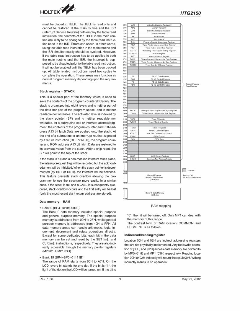
Stack register � STACK
This is a special part of the memory which is used to
save the contents of the program counter (PC) only. The
stack is organized into eight levels and is neither part of
the data nor part of the program space, and is neither
readable nor writeable. The activated level is indexed by
the stack pointer (SP) and is neither readable nor
writeable. At a subroutine call or interrupt acknowledg-
ment, the contents of the program counter and ROM ad-
dress A13 bit latch Data are pushed onto the stack. At
the end of a subroutine or an interrupt routine, signaled
by a return instruction (RET or RETI), the program coun-
ter and ROM address A13 bit latch Data are restored to
its previous value from the stack. After a chip reset, the
SP will point to the top of the stack.
If the stack is full and a non-masked interrupt takes place,
the interrupt request flag will be recorded but the acknowl-
edgment will be inhibited. When the stack pointer is decre-
mented (by RET or RETI), the interrupt will be serviced.
This feature prevents stack overflow allowing the pro-
grammer to use the structure more easily. In a similar
case, if the stack is full and a CALL is subsequently exe-
cuted, stack overflow occurs and the first entry will be lost
(only the most recent eight return address are stored).
Data memory � RAM
� Bank 0 (BP4~BP0=00000)
The Bank 0 data memory includes special purpose
and general purpose memory. The special purpose
memory is addressed from 00H to 2FH, while general
purpose memory is addressed from 40H to FFH. All
data memory areas can handle arithmetic, logic, in-
crement, decrement and rotate operations directly.
Except for some dedicated bits, each bit in the data
memory can be set and reset by the SET [m].i and
CLR [m].i instructions, respectively. They are also indi-
rectly accessible through the memory pointer registers
(MP0;01H, MP1;03H).
� Bank 15 (BP4~BP0=01111B)
The range of RAM starts from 80H to A7H. On the
LCD, every bit stands for one dot. If the bit is �1�, the
light of the dot on the LCD will be turned on. If the bit is
�0�, then it will be turned off. Only MP1 can deal with
the memory of this range.
The contrast form of RAM location, COMMON, and
SEGMENT is as follows.
Indirect addressing register
Location 00H and 02H are indirect addressing registers
that are not physically implemented. Any read/write opera-
tion of [00H] and [02H] access data memory are pointed to
by MP0 (01H) and MP1 (03H) respectively. Reading loca-
tion 00H or 02H indirectly will return the result 00H. Writing
indirectly results in no operation.
� 2 5
2 2 5
� � � .
� � � . �
� � � � 5
� 8 5
� � � �
� � � � �
3 � �
3 �
� � � �
� B � # % �
+ ! 5
" � 5
" 5
" 2 5
. ! 5
. " 5
. . 5
. � 5
. + 5
. / 5
. , 5
. � 5
. 4 5
. 9 5
. # 5
. 8 5
. � 5
. � 5
. 5
. 2 5
� ! 5
% � � � % � � * � � � � � � 7 * � � � � � � � �
� � � � � � * � � * # � � � � � � * � � � � � � �
� � � � * � � * C ! ! C 8 * - � � * � � . � " � ! * � � � � D !
E * � � � � � �
4 ! 5
# � 5
8 � � @ * " / * � � � � * � � � � � $; + ! * 8 $ � � =
� � � � � 7 * � � � � �8 � � @ * ! * � � � � * � � � � � $
; " 9 . * 8 $ � � =
! ! 5
! " 5
! . 5
! � 5
! + 5
! / 5
! , 5
! � 5
! 4 5
! 9 5
! # 5
! 8 5
! � 5
! � 5
! 5
! 2 5
" ! 5
" " 5
" . 5
" � 5
" + 5
" / 5
" , 5
" � 5
" 4 5
" 9 5
" # 5
" 8 5
" � 5
� # � !
� !
� # � "
� "
8
# � �
� %
� 8 %
� 8 % 5
3 � � �
� � # � � �
� � � �
� � � ! 5
� � � ! %
� � � ! �
#
# �
8
8 �
# * � � � * � � � � * � � � � � � � �
# * � � � * � � � � � � 7 * � � � � � � � �
8 * � � � * � � � � * � � � � � � � �
8 * � � � * � � � � � � 7 * � � � � � � � �
� � � � � � � � * # � � � � � � � � � * � � � � � � � � * !
� � � � � $ * � � � � � � * !
� � � � � � � � * # � � � � � � � � � * � � � � � � � � * "
� � � � � $ * � � � � � � * "
8 � � @ * � � � � � �
# � � � � � 7 � � � �
� � � � � � * � � � � � � � * % � F � � : - $ � � * � � � � � � � �
� � - 7 � * � � � � � � * % � F � � : � � � � � * 8 $ � � * � � � � � � � �
� � - 7 � * 5 � � & � � : � � � � � * 8 $ � � * � � � � � � � �
3 � � � & � � � * � � � � � * � � � � � * � � � � � � � * � � � � � � � �
� � � � � � * � � � � � � � �
� � � � � � � � * � � � � � � 7 * � � � � � � � �
� � � � � * � � � � � � � * ! * 5 � � & � � : � � � � � * 8 $ � � * � � � � � � � �
� � � � � * � � � � � � � * ! * % � F � � : � � � � � * 8 $ � � * � � � � � � � �
� � � � � * � � � � � � � * ! * � � � � � � 7 * � � � � � � � �
� � � � � 7 * � � � � �� � � � * � � � � � $
� � � � � � � � * � � � � � � 7 * 5 � � & � � : � � � � � * 8 $ � � * � � � � � � � �
� � - 7 � * � � � � � � * 5 � � & � � : � � � � � * 8 $ � � * � � � � � � � �
� � � � � * . * � � � � � � � �
� � � � � * . * � � � � � � 7 * � � � � � � � �
� � � � � * � * � � � � � � � �
� � � � � * � * � � � � � � 7 * � � � � � � � �
� B � � 7 * 2 � � � * � � � � 7 7 � � � � * � * � � � � � � 7
3 � * � � � � � � 7
3 � * � � � �
RAM mapping
HTG2150
Rev. 1.30 10 May 21, 2002
The function of data movement between two indirect ad-
dressing registers, is not supported. The memory
pointer registers, MP0 and MP1, are 8-bit registers
which can be used to access the data memory by com-
bining corresponding indirect addressing registers but
Bank 15 can use MP1 only.
Accumulator
The accumulator is closely related to ALU operations. It
is also mapped to location 05H of the data memory and
it can carry out immediate data operations. The data
movement between two data memories has to pass
through the accumulator.
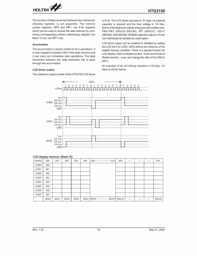
LCD driver output
The maximum output number of the HTG2150 LCD driver
is 8�40. The LCD driver bias type is �R� type, no external
capacitor is required and the bias voltage is 1/4 bias.
Some of the Segment outputs share pins with another pins,
PB4~PB7 (SEG33~SEG36), INT (SEG37), XOUT
(SEG38), XIN (SEG39). Whether segment output or I/O pin
can individually be decided by mask option.
LCD driver output can be enabled or disabled by setting
the LCD (bit 6 of LCDC; 2EH) without the influence of the
related memory condition. There is a special function for
LCD display, which is Rotate function. There are 8 kinds of
Rotate function, (user can change the data of the SS0 to
SS3.)
An example of an lcd driving waveform (1/8 duty, 1/4
bias) is shown below.
" . � + / , � 4
/ " . 5 6
� � � !
� � �
� � + * � � �
. � + * � � �
" � + * � � �
� �
� � � "
� � �
� � + * � � �
. � + * � � �
" � + * � � �
� �
� !
� � �
� � + * � � �
. � + * � � �
" � + * � � �
� �
� . 5 6
" . � + /" . � + / , � 4
# � � � � � �
� � � !
� � � "
� � � .
� � � �
� � � +
� � � /
� � � ,
� � � �
4 ! 5
8 � � !
8 � � "
8 � � .
8 � � �
8 � � +
8 � � /
8 � � ,
8 � � �
� !
4 " 5
� "
4 . 5
� .
4 � 5
� �
4 + 5 4 / 5 9 " 5
� / � " �� +
9 . 5
� " 4 � � 9
# � 5
� � � � � � � � � � � � � � � � � � � � � � � � � � � !
HTG2150
Rev. 1.30 11 May 21, 2002
Arithmetic and logic unit � ALU
This circuit performs 8-bit arithmetic and logic operation.
The ALU provides the following functions:
� Arithmetic operations (ADD, ADC, SUB,
SBC, DAA)
� Logic operations (AND, OR, XOR, CPL)
� Rotation (RL, RR, RLC, RRC)
� Increment and Decrement (INC, DEC)
� Branch decision (SZ, SNZ, SIZ, SDZ ....)
The ALU not only saves the results of a data operation but
also changes the status register.
Status register � STATUS
This 8-bit register (0AH) contains the zero flag (Z), carry
flag (C), auxiliary carry flag (AC), overflow flag (OV),
power down flag (PD) and watchdog time-out flag (TO).
It also records the status information and controls the oper-
ation sequence.
With the exception of the TO and PD flags, bits in the
status register can be altered by instructions like any
other register. Any data written into the status register
will not change the TO or PD flags. In addition it should
be noted that operations related to the status register
may give different results from those intended. The TO
and PD flags can only be changed by system power up,
Watchdog Timer overflow, executing the HALT instruc-
tion and clearing the Watchdog Timer.
The Z, OV, AC and C flags generally reflect the status of
the latest operations.
In addition, on entering the interrupt sequence or exe-
cuting the subroutine call, the status register will not be
automatically pushed onto the stack. If the contents of
status are important and if the subroutine can corrupt
the status register, precautions must be taken to save it
properly.
Register Bit No. Label Function
LCDC
0~5 � Can R/W (Default 000000B)
6 LCD Control the LCD output (0=disable; 1=enabled) (Default=1)
7 RC
LCD clock source select (Default=0)
1= 32768Hz crystal
0= system clock (note*)
LCDC register
Note: * When the mask option is selected to 32K xtal disable, user should set �0� to LCDC.7
But the 32K xtal cant be disabled in the HT-IDE2000 tools, so user should take care of this difference.
RotateDescription
SSL3 SSL2 SSL1 SSL0
x 0 0 0The Pad of common 0 is connected to common 0 and the Pad of common 1 is con-
nected to common 1 and so on.
x 0 0 1The Pad of common 0 is connected to common 1 and the Pad of common 1 is con-
nected to common 2 and so on.
x 0 1 0The Pad of common 0 is connected to common 2 and the Pad of common 1 is con-
nected to common 3 and so on.
x 0 1 1The Pad of common 0 is connected to common 3 and the Pad of common 1 is con-
nected to common 4 and so on.
x 1 0 0The Pad of common 0 is connected to common 4 and the Pad of common 1 is con-
nected to common 5 and so on.
x 1 0 1The Pad of common 0 is connected to common 5 and the Pad of common 1 is con-
nected to common 6 and so on.
x 1 1 0The Pad of common 0 is connected to common 6 and the Pad of common 1 is con-
nected to common 7 and so on.
x 1 1 1The Pad of common 0 is connected to common 7 and the Pad of common 1 is con-
nected to common 0 and so on.
2FH register
HTG2150
Rev. 1.30 12 May 21, 2002
Interrupt
The HTG2150 provides an external interrupt and a
PWM D/A interrupt and internal timer interrupts. The In-
terrupt Control register (INTC;0BH, INTCH;1EH) con-
tains the interrupt control bits to set the enable/disable
and the interrupt request flags.
Once an interrupt subroutine is serviced, all other inter-
rupts will be blocked (by clearing the EMI bit). This
scheme may prevent any further interrupt nesting. Other
interrupt requests may happen during this interval but
only the interrupt request flag is recorded. If a certain in-
terrupt needs servicing within the service routine, the
programmer may set the EMI bit and the corresponding
bit of the INTC to allow interrupt nesting. If the stack is
full, the interrupt request will not be acknowledged, even
if the related interrupt is enabled, until the SP is decre-
mented. If immediate service is desired, the stack must
be prevented from becoming full.
All these kinds of interrupt have a wake-up capability. As
an interrupt is serviced, a control transfer occurs by
pushing the program counter and A13 bit onto the stack
followed by a branch to subroutines at specified loca-
tions in the program memory. Only the program counter
and A13 bit are pushed onto the stack. If the contents of
the register and Status register (STATUS) are altered by
the interrupt service program which corrupt the desired
control sequence, the contents should be saved first.
External interrupt is triggered by a high to low transition
of INT and the related interrupt request flag (EIF; bit 4 of
INTC) will be set. When the interrupt is enabled, and the
stack is not full and the external interrupt is active, a sub-
routine call to location 04H will occur. The interrupt re-
quest flag (EIF) and EMI bits will be cleared to disable
other interrupts.
The internal timer counter 0 interrupt is initialized by set-
ting the timer counter 0 interrupt request flag (T0F; bit 5
of INTC), resulting from a timer 0 overflow. When the in-
terrupt is enabled, and the stack is not full and the T0F
bit is set, a subroutine call to location 08H will occur. The
related interrupt request flag (T0F) will be reset and the
EMI bit cleared to disable further interrupts.
The Timer 2/3 interrupts are operated in the same man-
ner as timer 0. While ET2I/ET3I and T2F/T3F are the re-
lated control bits and the related request flags of
TMR2/TMR3, which locate at bit0/bit1 and bit4/bi5 of the
INTCH respectively.
During the execution of an interrupt subroutine, other inter-
rupt acknowledgments are held until the RETI instruction is
executed or the EMI bit and the related interrupt control bit
are set to 1 ( if the stack is not full). To return from the inter-
Labels Bits Function
C 0
C is set if the operation results in a carry during an addition operation or if a borrow does not
take place during a subtraction operation; otherwise C is cleared. C is also affected by a rotate
through carry instruction.
AC 1AC is set if the operation results in a carry out of the low nibbles in addition or no borrow from
the high nibble into the low nibble in subtraction; otherwise AC is cleared.
Z 2 Z is set if the result of an arithmetic or logic operation is zero; otherwise Z is cleared.
OV 3OV is set if the operation results in a carry into the highest-order bit but not a carry out of the
highest-order bit, or vice versa; otherwise OV is cleared.
PD 4PD is cleared when either a system powers up or a CLR WDT instruction is executed. PD is set
by executing the HALT instruction.
TO 5TO is cleared by a system power-up or executing the CLR WDT or HALT instruction. TO is set
by a WDT time-out.
� 6, 7 Unused bit, read as �0�.
Status register
Register Bit No. Label Function
INTC
0 EMI Controls the (global) interrupt (1=enable; 0=disable)
1 EEI Controls the external interrupt (1=enable; 0=disable)
2 ET0I Controls the timer counter 0 interrupt (1=enable; 0=disable)
3 � Unused bit
4 EIF External interrupt request flag (1=active; 0=inactive)
5 T0F Internal timer counter 0 request flag (1=active; 0=inactive)
6, 7 � Unused bit
INTC register

HTG2150
Rev. 1.30 13 May 21, 2002
rupt subroutine, the RET or RETI instruction may be in-
voked. RETI will set the EMI bit to enable an interrupt
service, but RET will not.
Interrupts occurring in the interval between the rising
edges of two consecutive T2 pulses, will be serviced on
the latter of the two T2 pulses, if the corresponding inter-
rupts are enabled. In the case of simultaneous requests
the priorities applied are shown in the following table.
These can be masked by resetting the EMI bit.
No. Interrupt Source Priority Vector
a External interrupt 1 04H
b Timer counter 0 overflow 2 08H
d Timer 2 overflow 4 10H
e Timer 3 overflow 5 14H
f PWM D/A interrupt 6 18H
The timer counter 0 and Timer 2/3 interrupt request flag
(T0F/T2F/T3F), External interrupt request flag (EIF), PWM
D/A interrupt request flag (PWMF),Enable Timer 0/2/3 bit
(ET0I/ET2I/ET3I), enable PWM D/A interrupt (PWMI), En-
able external interrupt bit (EEI) and Enable master interrupt
bit (EMI) constitute an interrupt control register
(INTC/INTCH) which is located at 0BH/1EH in the data
memory. EMI, EEI, ET0I, ET2I, ET3I, PWMI are used to
control the enabling/disabling of interrupts. These bits
prevent the requested interrupt from being serviced.
Once the interrupt request flags (T0F, T2F, T3F, EIF,
PWMF) are set, they will remain in the INTC/INTCH reg-
ister until the interrupts are serviced or cleared by a soft-
ware instruction.
It is recommended that a program does not use the
�CALL subroutine� within the interrupt subroutine. Inter-
rupts often occur in an unpredictable manner or need to
be serviced immediately in some applications. If only
one stack is left and enabling the interrupt is not well
controlled, the �CALL subroutine� should not operate in
the interrupt subroutine as it will damage the original
control sequence.
Oscillator configuration
There are two oscillator circuits in the HTG2150.
The RC oscillator signal provides the internal system
clock. The HALT mode stops the system oscillator and
ignores any external signal to conserve power. Only the
RC oscillator is designed to drive the internal system
clock. The RTC oscillator provides the Timer 3 and LCD
driver clock source.
The RC oscillator needs an external resistor connected
between OSCI and VSS. The resistance value must
range from 50k� to 400k�.
However, the frequency of the oscillation may vary with
VDD, temperature and the chip itself due to process varia-
tions. It is, therefore, not suitable for timing sensitive oper-
ations where accurate oscillator frequency is desired.
There is another oscillator circuit designed for the real
time clock. In this case, only the 32768Hz crystal can be
applied. The crystal should be connected between XIN
and XOUT, and two external capacitors are required for
the oscillator circuit in order to get a stable frequency.
The RTC oscillator is used to provide clock source for
the LCD driver and Timer 3. It can be enabled or dis-
abled by mask option.
The WDT oscillator is a free running on-chip RC oscilla-
tor, requiring no external components. Even if the sys-
tem enters the power down mode, and the system clock
is stopped, the WDT oscillator still runs with a period of
approximately 78�s. The WDT oscillator can be dis-
abled by mask option to conserve power.
Register Bit No. Label Function
INTCH
0 ET2I Controls the Timer 2 interrupt (1=enable; 0=disable)
1 ET3I Controls the Timer 3 interrupt (1=enable; 0=disable)
2 PWMI PWM D/A interrupt (1=enable; 0=disable)
3 � Should be set as �0� always
4 T2F Internal Timer 2 request flag (1=active; 0=inactive)
5 T3F Internal Timer 3 request flag (1=active; 0=inactive)
6 PWMF PWM D/A flag (1=active; 0=inactive)
7 � Should be set as �0� always
INTCH register
� � � �
� � � * � � � � 7 7 � � � �
� � �
� � � �� . � , 4 5 6
� � * � � � � 7 7 � � � �
System and RTC oscillator
HTG2150
Rev. 1.30 14 May 21, 2002
Watchdog Timer � WDT
The WDT clock source is implemented by a dedicated RC
oscillator (WDT oscillator). This timer is designed to pre-
vent a software malfunction or sequence jumping to an un-
known location with unpredictable results. The Watchdog
Timer can be disabled by mask option. If the Watchdog
Timer is disabled, all the executions related to WDT result
in no operation.
When the internal WDT oscillator (RC oscillator with
78�s period normally) is enable, it is first divided by 256
(8 stages) to get the nominal time-out period of approxi-
mately 20ms. This time-out period may vary with tem-
perature, VDD and process variations. By invoking the
WDT prescaler, longer time-out periods can be realized.
Writing data to WS2, WS1, WS0 (bits 2,1,0 of the
WDTS) can give different time-out periods. If WS2,
WS1, WS0 are all equal to 1, the division ratio is up to
1:128, and the maximum time-out period is 2.6 seconds.
WS2 WS1 WS0 Division Ratio
0 0 0 1:1
0 0 1 1:2
0 1 0 1:4
0 1 1 1:8
1 0 0 1:16
1 0 1 1:32
1 1 0 1:64
1 1 1 1:128
WDTS register
The WDT overflow under normal operation will initialize
�chip reset� and set the status bit TO. Whereas in the
HALT mode, the overflow will initialize a �warm reset�only the PC and SP are reset to zero. To clear the WDT
contents (including the WDT prescaler), three methods
are adopted; external reset (a low level to RES), soft-
ware instructions, or a HALT instruction. The software in-
struction is �CLR WDT�, execution of the CLR WDT
instruction will clear the WDT.
Power down operation � HALT
The HALT mode is initialized by the HALT instruction
and results in the following...
� The system oscillator will turn off but the WDT oscilla-
tor keeps running (if the WDT oscillator is selected).
� The contents of the on-chip RAM and registers remain
unchanged.
� WDT and WDT prescaler will be cleared and do re-
counting again.
� All I/O ports maintain their original status.
� The PD flag is set and the TO flag is cleared.
The system can leave the HALT mode by means of an
external reset, an interrupt, an external falling edge sig-
nal on port A or a WDT overflow. An external reset
causes a device initialization and the WDT overflow per-
forms a �warm reset�. By examining the TO and PD flags,
the reason for chip reset can be determined. The PD flag
is cleared when the system powers up or upon executing
the CLR WDT instruction and is set when the HALT in-
struction is executed. The TO flag is set if the WDT
time-out occurs, and causes a wake-up that only resets
the PC and SP, the others maintain their original status.
The port A wake-up and interrupt methods can be con-
sidered as a continuation of normal execution. Each bit
in port A can be independently selected to wake up the
device by mask option. Awakening from an I/O port stim-
ulus, the program will resume execution of the next in-
struction. If awakening from an interrupt, two sequences
may happen. If the related interrupt is disabled or the in-
terrupt is enabled but the stack is full, the program will
resume execution at the next instruction. If the interrupt
is enabled and the stack is not full, the regular interrupt
response takes place.
Once a wake-up event occurs, it takes 1024 tSYS (sys-
tem clock period) to resume normal operation. In other
words, a dummy cycle period will be inserted after the
wake-up. If the wake-up results from an interrupt ac-
knowledge, the actual interrupt subroutine will be de-
layed by one more cycle. If the wake-up results in the
next instruction execution, this will be executed immedi-
ately after a dummy period has finished. If an interrupt
request flag is set to �1� before entering the HALT mode,
the wake-up function of the related interrupt will be dis-
abled.
To minimize power consumption, all I/O pins should be
carefully managed before entering the HALT status.
4 : - � � * � � � � � � �
3 � � * � � � � � 7 � �
� : - � � * � � � � � � �
4 : � � : " * � � �
3 � � * � � � � : � � �
3 � ! 0 3 � .
3 � �
� � �
Watchdog Timer
HTG2150
Rev. 1.30 15 May 21, 2002
Reset
There are three ways in which a reset can occur:
� RES reset during normal operation
� RES reset during HALT
� WDT time-out reset during normal operation
The WDT time-out during HALT is different from other
chip reset conditions, since it can perform a �warm re -
set� that just resets the PC and SP, leaving the other cir-
cuits in their original state. Some registers remain un-
changed during other reset conditions. Most registers
are reset to the �initial condition� when the reset condi-
tions are met. By examining the PD and TO flags, the
program can distinguish between different �chip resets�.
TO PD RESET Conditions
0 0 RES reset during power-up
u u RES reset during normal operation
0 1 RES wake-up HALT
1 u WDT time-out during normal operation
1 1 WDT wake-up HALT
Note: �u� means �unchanged�
To guarantee that the system oscillator has started and
stabilized, the SST (System Start-up Timer) provides an
extra-delay of 1024 system clock pulses when the sys-
tem powers up or awakes from the HALT state.
When a system power-up occurs, the SST delay is
added during the reset period. But when the reset co-
mes from the RES pin, the SST delay is disabled. Any
wake-up from HALT will enable the SST delay.
The functional unit chip reset status are shown below.
PC 000H
Interrupt Disable
Prescaler Clear
WDTClear. After master reset,
WDT begins counting
Timer (0/2/3) Off
LCD Display Enable
Pull-high of RESB with
Input/output Ports Input mode
SP Points to the top of the stack
Timer 0
The timer 0 contains 16-bit programmable count-up
counters and the clock source come from the system
clock divided by 4.
There are three registers related to timer counter 0;
TMR0H (0CH), TMR0L (0DH), TMR0C (0EH). Writing
TMR0L only writes the data into a low byte buffer, and
writing TMR0H will write the data and the contents of the
low byte buffer into the timer 0 preload register (16-bit)
simultaneously. The timer 0 preload register is changed
by writing TMR0H operations and writing TMR0L will
keep the timer 0 preload register unchanged.
Reading TMR0H will also latch the TMR0L into the low
byte buffer to avoid the false timing problem. Reading
TMR0L returns the contents of the low byte buffer. In
other words, the low byte of timer counter 0 cannot be
read directly. It must read the TMR0H first to make the
low byte contents of timer 0 be latched into the buffer.
The TMR0C is the timer 0 control register, which defines
the timer 0 options.
The timer counter control registers define the operating
mode, counting enable or disable and active edge.
If the timer counter starts counting, it will count from the
current contents in the timer counter to FFFFH. Once an
overflow occurs, the counter is reloaded from the timer
counter preload register and generates the correspond-
ing interrupt request flag (T0F; bit of INTC) at the same
time.
To enable the counting operation, the Timer ON bit (TON;
bit 4 of TMR0C) should be set to 1. The overflow of the
timer counter is one of the wake-up sources. No matter
� � � �� �
� � �
� � � * � � � � : � � �
� & � * * � � � � �
Reset timing chart
� �
� � �
Reset circuit
3 � �
5 # % �
3 � �
� � � � : � � �� � � � �
� �
� � 7 �� � � � �
3 � � � * � � � � �
� F � � : � � * � � � � � � � � �
� � �" ! : � � � � �
� � 7 � * � � � � � � �� � � "
Reset configuration

HTG2150
Rev. 1.30 16 May 21, 2002
what the operation mode is, writing a 0 to ET0I can dis-
able the corresponding interrupt service.
In the case of timer counter OFF condition, writing data
to the timer counter preload register will also reload that
data to the timer counter. But if the timer counter is
turned on, data written to the timer counter will only
be kept in the timer counter preload register. The
timer counter will still operate until overflow occurs.
When the timer counter (reading TMR0H) is read, the
clock will be blocked to avoid errors. As this may re-
sults in a counting error, this must be taken into con-
sideration by the programmer.
The state of the registers is summarized in the following table:
RegisterReset
(Power On)WDT Time-out
(Normal Operation)RES Reset
(Normal Operation)RES Reset
(HALT)WDT Time-out
(HALT)
TMR0H xxxx xxxx uuuu uuuu uuuu uuuu uuuu uuuu uuuu uuuu
TMR0L xxxx xxxx uuuu uuuu uuuu uuuu uuuu uuuu uuuu uuuu
TMR0C 00-0 1--- 00-0 1--- 00-0 1--- 00-0 1--- uu-u u---
TMR2 xxxx xxxx uuuu uuuu uuuu uuuu uuuu uuuu uuuu uuuu
TMR2C 00-0 1000 00-0 1000 00-0 1000 00-0 1000 uu-u uuuu
TMR3 xxxx xxxx uuuu uuuu uuuu uuuu uuuu uuuu uuuu uuuu
TMR3C 00-0 1000 00-0 1000 00-0 1000 00-0 1000 uu-u uuuu
INTCH 0000 0000 0000 0000 0000 0000 0000 0000 uuuu uuuu
TBHP xxxx xxxx uuuu uuuu uuuu uuuu uuuu uuuu uuuu uuuu
Program Counter 0000H 0000H 0000H 0000H 0000H
MP0 xxxx xxxx uuuu uuuu uuuu uuuu uuuu uuuu uuuu uuuu
MP1 xxxx xxxx uuuu uuuu uuuu uuuu uuuu uuuu uuuu uuuu
ACC xxxx xxxx uuuu uuuu uuuu uuuu uuuu uuuu uuuu uuuu
TBLP xxxx xxxx uuuu uuuu uuuu uuuu uuuu uuuu uuuu uuuu
TBLH xxxx xxxx uuuu uuuu uuuu uuuu uuuu uuuu uuuu uuuu
STATUS --00 xxxx --1u uuuu --uu uuuu --01 uuuu --11 uuuu
BP 0000 0000 0000 0000 0000 0000 0000 0000 uuuu uuuu
LCDC 0100 0000 0100 0000 0100 0000 0100 0000 uuuu uuuu
INTC 0000 0000 0000 0000 0000 0000 0000 0000 uuuu uuuu
WDTS 0000 0111 0000 0111 0000 0111 0000 0111 uuuu uuuu
PA 1111 1111 1111 1111 1111 1111 1111 1111 uuuu uuuu
PAC 1111 1111 1111 1111 1111 1111 1111 1111 uuuu uuuu
PB 1111 0000 1111 0000 1111 0000 1111 0000 uuuu uuuu
PBC 1111 0000 1111 0000 1111 0000 1111 0000 uuuu 0000
COMR 0000 0000 0000 0000 0000 0000 0000 0000 uuuu uuuu
PWMC 1111 1111 1111 1111 1111 1111 1111 1111 uuuu uuuu
PWM xxxx xxxx xxxx xxxx xxxx xxxx xxxx xxxx uuuu uuuu
XTALC 0000 0000 0000 0000 0000 0000 0000 0000 uuuu uuuu
Note: �*� means �warm reset��u� means �unchanged��x� means �unknown�
� � � � � * � � � � � � � * ! � � 7 � � � * � � � � � � � �
� � � � �� � � � � � � * !
� � � � * 8 � �
� � 7 � � �
� 1 � � ' 7 � F� � * � � � � � � � �
% � F * 8 $ � �8 � ' ' � �
� $ � � � �� 7 � � @ � +
Timer counter 0

HTG2150
Rev. 1.30 17 May 21, 2002
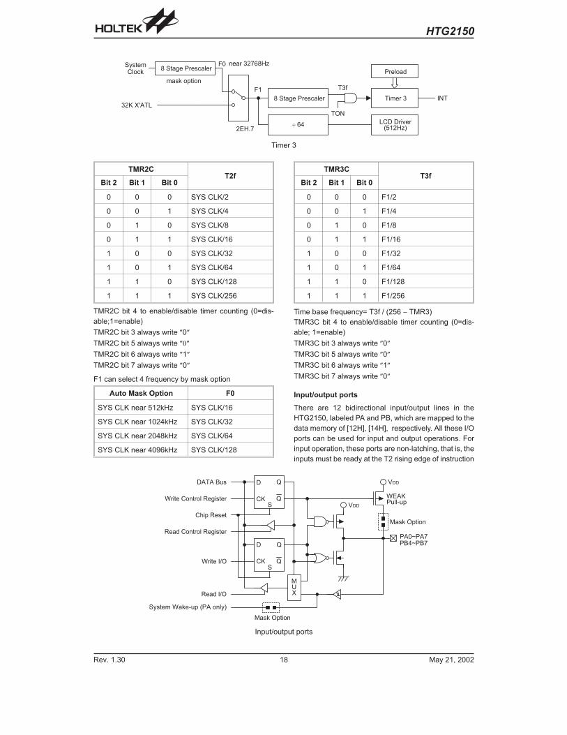
Timer 2/3
Timer 2 is an 8-bit counter, and its clock source comes
from the system clock divided by an 8-stage prescaler.
There are two registers related to Timer 2 ; TMR2 (21H)
and TMR2C (22H). Two physical registers are mapped
to TMR2 location; writing TMR2 makes the starting
value be placed in the Timer 2 preload register and
reading the TMR2 gets the contents of the Timer 2 coun-
ter. The TMR2C is a control register, which defines the
division ratio of the prescaler and counting enable or
disable.
Writing data to B2, B1 and B0 (bits 2, 1, 0 of TMR2C)
can yield various clock sources.
Once the Timer 2 starts counting, it will count from the
current contents in the counter to FFH. Once an over-
flow occurs, the counter is reloaded from a preload reg-
ister, and generates an interrupt request flag (T2F; bit 4
of INTCH). To enable the counting operation, the timer
On bit (TON; bit 4 of TMR2C) should be set to �1�. For
proper operation, bit 6 of TMR2C should be set to �1�
and bit 3, bit7 should be set to �0�.
The Timer 2 can also be used as PFD output by setting
PWM1 and PWM2 to be PFD and PFDB output respec-
tively by 2FH.7 and 2FH.6. When the PFD/PFDB func-
tion is selected, setting 2FH.4/2FH.5 to �1� will enable
the PFD/PFDB output and setting 2FH.4/2FH.5 to �0�will disable the PFD/PFDB output. PFD Frequency:
T2f/[256-TMR2)�2]
Timer 3 has the same structure and operating manner
with Timer 2, except for clock source and PFD function.
The Timer 3 can be used as a time base to generate a
regular internal interrupt. The clock source of Timer 3
can come from RTC OSC (XTAL 32kHz) or system
clock divided by an 8-stage prescaler. If the RTC mask
option is enabled, a 32kHz crystal is needed across XIN
and XOUT pins. The 32kHz signal is processed by an
8-stage prescaler to yield various counting clock for
Timer 3. There are 2 registers related to Timer 3; TMR3
(24H) and TMR3C (25H). Writing data to B2, B1, B0 (bit
2, 1, 0 of TMR3C) can yield various counting clock.
Label Bits Function
� 0~2 Unused bit, read as �0�.
TE 3To define the TMR0 active edge of the timer counter
(0=active on low to high; 1=active on high to low)
TON 4 To enable/disable timer counting (0=disabled; 1=enabled)
� 5 Unused bit, read as �x�.
TM0, TM1 6, 7 0, 1=Internal clock
TMR0C register
� ) � * � % ( *4 : � � � � � � � � � � 7 � �
� � � � � * . � � 7 � � � * � � � � � � � �
� � � � � * .
� � � � * 8 � �
� � 7 � � �
� 1 � � ' 7 � F� � �
. 2 5 G +
� � * � � � � � � � �� . '
� .
. 2 5 G / 3 � .
. 2 5 G �
3 � � # � .
3 � "
. 2 5 G ,
3 � � # � "
Timer 2
Label Bits Function
SSL 3~0 3~0 LCD common used
PFD 4 To enable/disable PFD output (0=disable; 1=enable)
PFDB 5 To enable/disable PFDB output (0=disable; 1=enable)
PWM1 6 To select PFDB/PWM1 output (0=PWM1; 1=PFDB)
PWM2 7 To select PFD/PWM2 output (0=PWM2; 1=PFD)
2FH register
HTG2150
Rev. 1.30 18 May 21, 2002
� � � � � * �
� � �
� � �
� � 7 � � �
4 * � � � � � * � � � � � 7 � �
% � � * � � � 1 � �; / " . 5 6 =
� . ( * � B # � %
. 5 G �
4 * � � � � � * � � � � � 7 � �� $ � � � �� 7 � � @
2 !
2 " � � '
� � � � * � . � , 4 5 6
� � , +
� � � @ * � � � � �
Timer 3
TMR2CT2f
Bit 2 Bit 1 Bit 0
0 0 0 SYS CLK/2
0 0 1 SYS CLK/4
0 1 0 SYS CLK/8
0 1 1 SYS CLK/16
1 0 0 SYS CLK/32
1 0 1 SYS CLK/64
1 1 0 SYS CLK/128
1 1 1 SYS CLK/256
TMR2C bit 4 to enable/disable timer counting (0=dis-
able;1=enable)
TMR2C bit 3 always write �0�
TMR2C bit 5 always write ���
TMR2C bit 6 always write �1�
TMR2C bit 7 always write �0�
F1 can select 4 frequency by mask option
Auto Mask Option F0
SYS CLK near 512kHz SYS CLK/16
SYS CLK near 1024kHz SYS CLK/32
SYS CLK near 2048kHz SYS CLK/64
SYS CLK near 4096kHz SYS CLK/128
TMR3CT3f
Bit 2 Bit 1 Bit 0
0 0 0 F1/2
0 0 1 F1/4
0 1 0 F1/8
0 1 1 F1/16
1 0 0 F1/32
1 0 1 F1/64
1 1 0 F1/128
1 1 1 F1/256
Time base frequency= T3f / (256 � TMR3)
TMR3C bit 4 to enable/disable timer counting (0=dis-
able; 1=enable)
TMR3C bit 3 always write �0�
TMR3C bit 5 always write �0�
TMR3C bit 6 always write �1�
TMR3C bit 7 always write �0�
Input/output ports
There are 12 bidirectional input/output lines in the
HTG2150, labeled PA and PB, which are mapped to the
data memory of [12H], [14H], respectively. All these I/O
ports can be used for input and output operations. For
input operation, these ports are non-latching, that is, the
inputs must be ready at the T2 rising edge of instruction
H
�
� (�
H
�
� (�
H
���
� # � # * 8 � �
3 � � � � * � � � � � � 7 * � � � � � � � �
� & � * � � � � �
� � � � * � � � � � � 7 * � � � � � � � �
3 � � � � * � � �
� � � � * � � �
� $ � � � � * 3 � @ � : � * ; # * � � 7 $ =
3 # ( � 7 7 : �
# ! 0 # � 8 + 0 8 �
� � � @ * � � � � �
� � � @ * � � � � �
� � �
H
� � �
Input/output ports

HTG2150
Rev. 1.30 19 May 21, 2002
MOV A,[m] (m=12H, 14H). For output operation, all data
is latched and remains unchanged until the output latch
is rewritten.
Each I/O line has its own control register (PAC, PBC) to
control the input/output configuration. With this control
register, CMOS output or schmitt trigger input with or
without pull-high resistor structures can be reconfigured
dynamically under software control. To function as an in-
put, the corresponding latch of the control register must
write �1�. The pull-high resistance will exhibit automati-
cally if the pull-high option is selected. The input source
also depends on the control register. If the control regis-
ter bit is �1�, the input will read the pad state. If the con-
trol register bit is �0�, the contents of the latches will
move to the internal bus. The latter is possible in
�read-modify-write� instruction. For output function,
CMOS is the only configuration. These control registers
are mapped to locations 13H, 15H.
After a chip reset, these input/output lines stay at
schmitt trigger input with pull-high resistor. Each bit of
these input/output latches can be set or cleared by the
SET [m].i or CLR [m].i (m=12H, 14H) instruction.
Some instructions first input data and then follow the
output operations. For example, the SET [m].i, CLR
[m].i, CPL [m] and CPLA [m] instructions read the entire
port states into the CPU, execute the defined operations
(bit-operation), and then write the results back to the
latches or the accumulator.
Each line of port A has the capability to wake-up the de-
vice. Port B are share pad, each pin function are defined
by mask option, the PB7 shares with SEG36. The PB6,
PB5 and PB4 share with SEG35, SEG34 and SEG33. If
the segment output is selected, the related I/O register
(PB) cannot be used as general purpose register. Reading
the register will result to an unknown state.
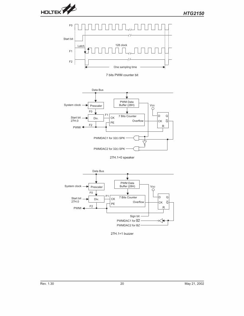
PWM interface
The HTG2150 provides an 8 bit (bit 7 is a sign bit) PWM
D/A interface, which is good for speech synthesis. The
user can record or synthesize the sound and digitize it
into the program ROM. These sound could be played
back in sequence of the functions as designed by the in-
ternal program ROM. There are several algorithms that
can be used in the HTG2150, they are ... PCM, �LAW,
DPCM, ADPCM..... .
The PWM circuit provides two pad outputs: PWM2,
PWM1 which can directly drive a piezo or a 32� speaker
without adding any external element. Refer to the Appli-
cation Circuits.
The PWM clock source comes from the system clock di-
vided by a 3-bit prescaler. Setting data to P0, P1 and P2
(bit 3, 4, 5 of 27H) can yield various clock sources. The
clock source are use for PWM modulating clock and
sampling clock. After setting the start bit (bit 0 27H) and
the next falling edge coming from the prescaler, the
�DIV� will generate a serial clock to PWM counter for
modulating and PWMI for interrupt. The PWM counter
latch data at the first �F1� clock falling edge and the start
counter at �F1� rising edge. The �F2� clock is synchro-
nous with the first �F1� clock and it is also connected to
the PWM output latch. In setting the �start bit� initial sta-
tus, the �PWM1 DAC� outputs a �high� level and change
the output status to �LOW� while the �7 bits counter�overflows.
BZ/SP6/7Bit
F1F2
(SamplingRate
Device
0 0 F0 F0/64 32� speaker
0 1 F0 F0/128 32� speaker
1 0 F0 F0/64 Buzzer/8� speaker
1 1 F0 F0/128 Buzzer/8� speaker
Note: F1: for PWM modulation clock and F2 for
sampling clock.
F0: system /[n+1] n=0~7
(n:3 bits preload counter)
On the above table, we can easily see that the sampling
rate is dependent on the system clock. If start bit is set to
�0�, the PWM2 and PWM1 will output a GND level volt-
age.
Label Bits Function
D/A 0 D/A control. 0:start ; 1:stop
BZ/SP 1Output driver select
1:Buzzer ; 0:speaker
Bit 2PWM counter bit select
1:7 bits ; 0:6 bits
P0~P2 3~5
3 bits preload counter,
bit 5/4/3:000B~111B (0~7)
bit 3:LSB
D0, D1 6, 7 PWMI
D0 D1 PWM Interrupt
0 0 1
0 1 2
1 0 4
1 1 8
PWM control register
bit0 bit1 bit2 bit3 bit4 bit5 bit6 bit7
7 bit D0 D1 D2 D3 D4 D5 D6 D7
6 bit X D1 D2 D3 D4 D5 D6 D7
Note: X means dont care.
bit7: Sign bit
PWM data buffer
HTG2150
Rev. 1.30 20 May 21, 2002
2 !
� � � � � * - � �
2 "
2 .
� � � * � � � 7 � � � * � � � �
" . 4 * � 7 � � @% � � � &
7 bits PWM counter bit
� $ � � � � * � 7 � � @ � � � � � 7 � �
3 � * � � � �8 � ' ' � � * ; . 4 5 =
� * 8 � � � * � � � � � � �
� � � � * 8 � �
� 1 � � ' 7 � F
3 � � # � " * ' � � * � . � * � (
2 !
� � � � � * - � �. � 5 G !
� � 1 G
3 � �2 .
� (
2 "
� � �
�
� (
H
�
H
3 � � # � . * ' � � * � . � * � (
27H.1=0 speaker
� $ � � � � * � 7 � � @ � � � � � 7 � �
3 � * � � � �8 � ' ' � � * ; . 4 5 =
� * 8 � � � * � � � � � � �
� � � � * 8 � �
� 1 � � ' 7 � F
2 !
� � � � � * - � �. � 5 G !
� � 1 G
3 � �2 .
� (
� � � � * - � �
2 "
3 � � # � " * ' � � * 8 I
3 � � # � . * ' � � * 8 I
� � �
�
� (
H
�
H
27H.1=1 buzzer

HTG2150
Rev. 1.30 21 May 21, 2002
Mask option
The following shows many kinds of mask options in the HTG2150. All the mask options must be defined on order to en-
sure proper system functioning.
No. Mask Option
1WDT enable/disable selection.
WDT can be enabled or disabled by mask option.
2Wake-up selection. This option defines the wake-up activity. External I/O pins (PA only) all have the capabil-
ity to wake-up the chip from a HALT mode by a following edge.
3External interrupt input pin share with other function selection.
INT/SEG37: INT can be set as an external interrupt input pin or LCD segment output pin.
4
I/O pins share with other function selection.
PB4/SEG33, PB5/SEG34, PB6/SEG35, PB7/SEG36: PB4, PB5, PB6, PB7 can be set as I/O pins or LCD
segment output pins.
5
Segment output pins share with other function selection.
XIN/SEG39, XOUT/SEG38: SEG38, SEG39 ban be set as LCD segment output pins or XIN, XOUT pins be
connected to a 32768Hz crystal.
6LCD bias register selection. This option describes the LCD bias current. There are three types of selection. *
� Selectable as small, middle or large current.
Note: * " � � � � � # $ � � � � %
" " ! @ �
� � + * � � �
" " ! @ �
" " ! @ �
" � + * � � �
" " ! @ �
� �
. � + * � � �
& � � � � � � # $ � � � � %
, ! @ �
� � + * � � �
" � + * � � �
� �
. � + * � � �
� � � ' � � # $ � � � � %
" ! @ �
� � + * � � �
" � + * � � �
� �
. � + * � � �
, ! @ �
, ! @ �
, ! @ �
" ! @ �
" ! @ �
" ! @ �
� � � � � � � � �
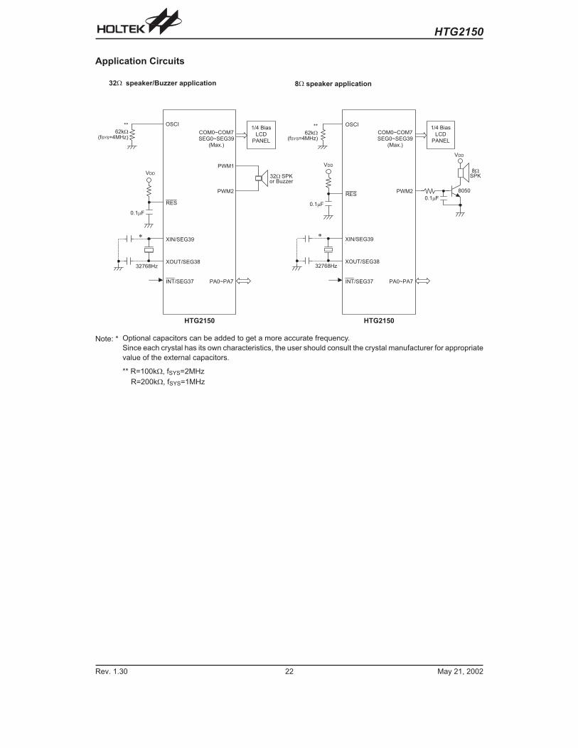
Application Circuits
Note: * Optional capacitors can be added to get a more accurate frequency.
Since each crystal has its own characteristics, the user should consult the crystal manufacturer for appropriate
value of the external capacitors.
** R=100k�, fSYS=2MHz
R=200k�, fSYS=1MHz
HTG2150
Rev. 1.30 22 May 21, 2002
� � � �
# ! 0 # �
( � � � � � � � � � � ) � $ * * � � � � � � � � # � % � � � + � � � � � � � � � � � � � � # � % � � �
� � � � � � �
� �
� � � � � � �
� � � ! 0 � � � �� ! 0 � � 9
; � � > G =
" � + * 8 � � �
% � �
# � %
� � � �
# ! 0 # �
� � � � � � �
� �
� � � � � � �
" � + * 8 � � �
% � �
# � %
� � �
� � � 3 � "
3 � . 3 � . 4 ! / !
4 �� (
� � �
� . � � � (� � * 8 � 6 6 � �
� � � � � � 9
� � � � � � � 4� . � , 4 5 6
� � � � � � 9
� � � � � � � 4� . � , 4 5 6
� �
� � � ! 0 � � � �� ! 0 � � 9
; � � > G =
J J
, . @ �; ' � ) � D + � 5 6 =
! G " � 2
! G " � 2
J J
, . @ �; ' � ) � D + � 5 6 =
! G " � 2
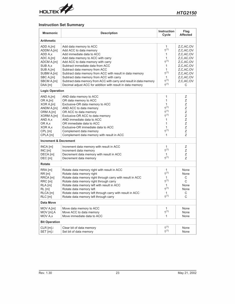
Instruction Set Summary
Mnemonic DescriptionInstruction
CycleFlag
Affected
Arithmetic
ADD A,[m]
ADDM A,[m]
ADD A,x
ADC A,[m]
ADCM A,[m]
SUB A,x
SUB A,[m]
SUBM A,[m]
SBC A,[m]
SBCM A,[m]
DAA [m]
Add data memory to ACC
Add ACC to data memory
Add immediate data to ACC
Add data memory to ACC with carry
Add ACC to data memory with carry
Subtract immediate data from ACC
Subtract data memory from ACC
Subtract data memory from ACC with result in data memory
Subtract data memory from ACC with carry
Subtract data memory from ACC with carry and result in data memory
Decimal adjust ACC for addition with result in data memory
1
1(1)
1
1
1(1)
1
1
1(1)
1
1(1)
1(1)
Z,C,AC,OV
Z,C,AC,OV
Z,C,AC,OV
Z,C,AC,OV
Z,C,AC,OV
Z,C,AC,OV
Z,C,AC,OV
Z,C,AC,OV
Z,C,AC,OV
Z,C,AC,OV
C
Logic Operation
AND A,[m]
OR A,[m]
XOR A,[m]
ANDM A,[m]
ORM A,[m]
XORM A,[m]
AND A,x
OR A,x
XOR A,x
CPL [m]
CPLA [m]
AND data memory to ACC
OR data memory to ACC
Exclusive-OR data memory to ACC
AND ACC to data memory
OR ACC to data memory
Exclusive-OR ACC to data memory
AND immediate data to ACC
OR immediate data to ACC
Exclusive-OR immediate data to ACC
Complement data memory
Complement data memory with result in ACC
1
1
1
1(1)
1(1)
1(1)
1
1
1
1(1)
1
Z
Z
Z
Z
Z
Z
Z
Z
Z
Z
Z
Increment & Decrement
INCA [m]
INC [m]
DECA [m]
DEC [m]
Increment data memory with result in ACC
Increment data memory
Decrement data memory with result in ACC
Decrement data memory
1
1(1)
1
1(1)
Z
Z
Z
Z
Rotate
RRA [m]
RR [m]
RRCA [m]
RRC [m]
RLA [m]
RL [m]
RLCA [m]
RLC [m]
Rotate data memory right with result in ACC
Rotate data memory right
Rotate data memory right through carry with result in ACC
Rotate data memory right through carry
Rotate data memory left with result in ACC
Rotate data memory left
Rotate data memory left through carry with result in ACC
Rotate data memory left through carry
1
1(1)
1
1(1)
1
1(1)
1
1(1)
None
None
C
C
None
None
C
C
Data Move
MOV A,[m]
MOV [m],A
MOV A,x
Move data memory to ACC
Move ACC to data memory
Move immediate data to ACC
1
1(1)
1
None
None
None
Bit Operation
CLR [m].i
SET [m].i
Clear bit of data memory
Set bit of data memory
1(1)
1(1)None
None
HTG2150
Rev. 1.30 23 May 21, 2002
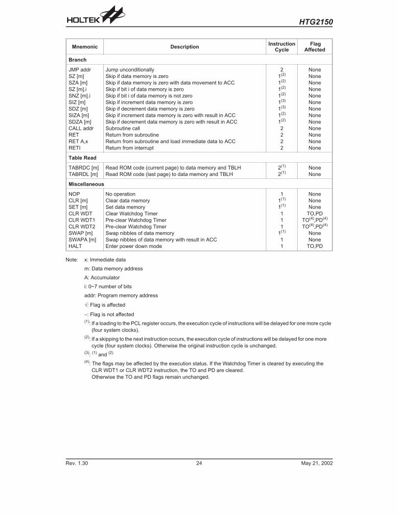
Mnemonic DescriptionInstruction
CycleFlag
Affected
Branch
JMP addr
SZ [m]
SZA [m]
SZ [m].i
SNZ [m].i
SIZ [m]
SDZ [m]
SIZA [m]
SDZA [m]
CALL addr
RET
RET A,x
RETI
Jump unconditionally
Skip if data memory is zero
Skip if data memory is zero with data movement to ACC
Skip if bit i of data memory is zero
Skip if bit i of data memory is not zero
Skip if increment data memory is zero
Skip if decrement data memory is zero
Skip if increment data memory is zero with result in ACC
Skip if decrement data memory is zero with result in ACC
Subroutine call
Return from subroutine
Return from subroutine and load immediate data to ACC
Return from interrupt
2
1(2)
1(2)
1(2)
1(2)
1(3)
1(3)
1(2)
1(2)
2
2
2
2
None
None
None
None
None
None
None
None
None
None
None
None
None
Table Read
TABRDC [m]
TABRDL [m]
Read ROM code (current page) to data memory and TBLH
Read ROM code (last page) to data memory and TBLH
2(1)
2(1)None
None
Miscellaneous
NOP
CLR [m]
SET [m]
CLR WDT
CLR WDT1
CLR WDT2
SWAP [m]
SWAPA [m]
HALT
No operation
Clear data memory
Set data memory
Clear Watchdog Timer
Pre-clear Watchdog Timer
Pre-clear Watchdog Timer
Swap nibbles of data memory
Swap nibbles of data memory with result in ACC
Enter power down mode
1
1(1)
1(1)
1
1
1
1(1)
1
1
None
None
None
TO,PD
TO(4),PD(4)
TO(4),PD(4)
None
None
TO,PD
Note: x: Immediate data
m: Data memory address
A: Accumulator
i: 0~7 number of bits
addr: Program memory address
�: Flag is affected
�: Flag is not affected
(1): If a loading to the PCL register occurs, the execution cycle of instructions will be delayed for one more cycle
(four system clocks).
(2): If a skipping to the next instruction occurs, the execution cycle of instructions will be delayed for one more
cycle (four system clocks). Otherwise the original instruction cycle is unchanged.
(3):
(1)and
(2)
(4): The flags may be affected by the execution status. If the Watchdog Timer is cleared by executing the
CLR WDT1 or CLR WDT2 instruction, the TO and PD are cleared.
Otherwise the TO and PD flags remain unchanged.
HTG2150
Rev. 1.30 24 May 21, 2002
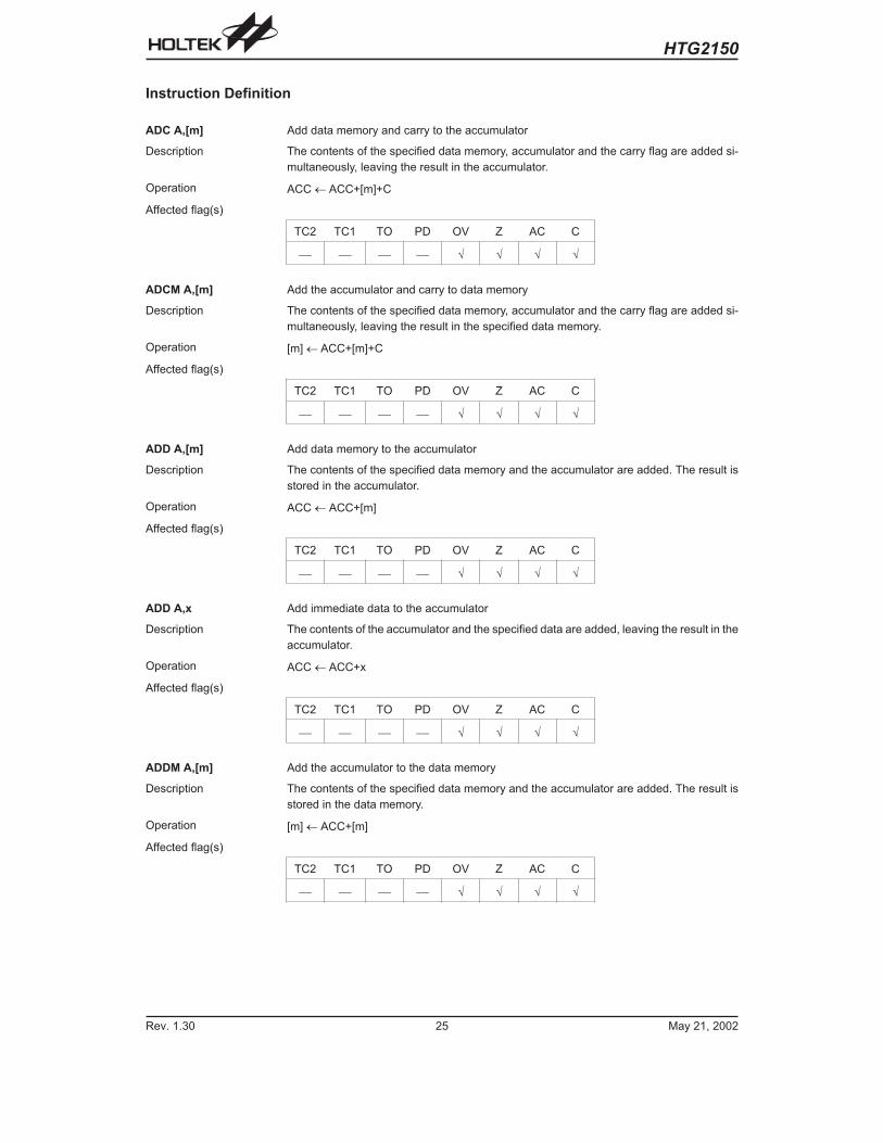
Instruction Definition
ADC A,[m] Add data memory and carry to the accumulator
Description The contents of the specified data memory, accumulator and the carry flag are added si-
multaneously, leaving the result in the accumulator.
Operation ACC ACC+[m]+C
Affected flag(s)
TC2 TC1 TO PD OV Z AC C
� � � � � � � �
ADCM A,[m] Add the accumulator and carry to data memory
Description The contents of the specified data memory, accumulator and the carry flag are added si-
multaneously, leaving the result in the specified data memory.
Operation [m] ACC+[m]+C
Affected flag(s)
TC2 TC1 TO PD OV Z AC C
� � � � � � � �
ADD A,[m] Add data memory to the accumulator
Description The contents of the specified data memory and the accumulator are added. The result is
stored in the accumulator.
Operation ACC ACC+[m]
Affected flag(s)
TC2 TC1 TO PD OV Z AC C
� � � � � � � �
ADD A,x Add immediate data to the accumulator
Description The contents of the accumulator and the specified data are added, leaving the result in the
accumulator.
Operation ACC ACC+x
Affected flag(s)
TC2 TC1 TO PD OV Z AC C
� � � � � � � �
ADDM A,[m] Add the accumulator to the data memory
Description The contents of the specified data memory and the accumulator are added. The result is
stored in the data memory.
Operation [m] ACC+[m]
Affected flag(s)
TC2 TC1 TO PD OV Z AC C
� � � � � � � �
HTG2150
Rev. 1.30 25 May 21, 2002
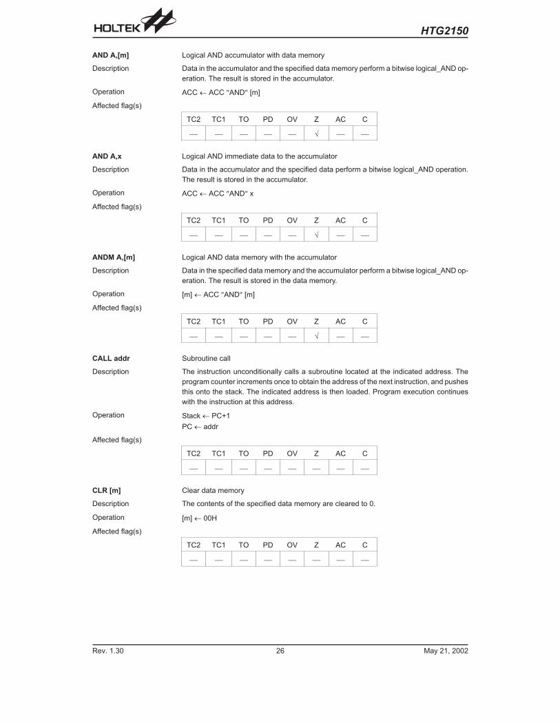
AND A,[m] Logical AND accumulator with data memory
Description Data in the accumulator and the specified data memory perform a bitwise logical_AND op-
eration. The result is stored in the accumulator.
Operation ACC ACC �AND� [m]
Affected flag(s)
TC2 TC1 TO PD OV Z AC C
� � � � � � � �
AND A,x Logical AND immediate data to the accumulator
Description Data in the accumulator and the specified data perform a bitwise logical_AND operation.
The result is stored in the accumulator.
Operation ACC ACC �AND� x
Affected flag(s)
TC2 TC1 TO PD OV Z AC C
� � � � � � � �
ANDM A,[m] Logical AND data memory with the accumulator
Description Data in the specified data memory and the accumulator perform a bitwise logical_AND op-
eration. The result is stored in the data memory.
Operation [m] ACC �AND� [m]
Affected flag(s)
TC2 TC1 TO PD OV Z AC C
� � � � � � � �
CALL addr Subroutine call
Description The instruction unconditionally calls a subroutine located at the indicated address. The
program counter increments once to obtain the address of the next instruction, and pushes
this onto the stack. The indicated address is then loaded. Program execution continues
with the instruction at this address.
Operation Stack PC+1
PC addr
Affected flag(s)
TC2 TC1 TO PD OV Z AC C
� � � � � � � �
CLR [m] Clear data memory
Description The contents of the specified data memory are cleared to 0.
Operation [m] 00H
Affected flag(s)
TC2 TC1 TO PD OV Z AC C
� � � � � � � �
HTG2150
Rev. 1.30 26 May 21, 2002

CLR [m].i Clear bit of data memory
Description The bit i of the specified data memory is cleared to 0.
Operation [m].i 0
Affected flag(s)
TC2 TC1 TO PD OV Z AC C
� � � � � � � �
CLR WDT Clear Watchdog Timer
Description The WDT is cleared (clears the WDT). The power down bit (PD) and time-out bit (TO) are
cleared.
Operation WDT 00H
PD and TO 0
Affected flag(s)
TC2 TC1 TO PD OV Z AC C
� � 0 0 � � � �
CLR WDT1 Preclear Watchdog Timer
Description Together with CLR WDT2, clears the WDT. PD and TO are also cleared. Only execution of
this instruction without the other preclear instruction just sets the indicated flag which im-
plies this instruction has been executed and the TO and PD flags remain unchanged.
Operation WDT 00H*
PD and TO 0*
Affected flag(s)
TC2 TC1 TO PD OV Z AC C
� � 0* 0* � � � �
CLR WDT2 Preclear Watchdog Timer
Description Together with CLR WDT1, clears the WDT. PD and TO are also cleared. Only execution of
this instruction without the other preclear instruction, sets the indicated flag which implies
this instruction has been executed and the TO and PD flags remain unchanged.
Operation WDT 00H*
PD and TO 0*
Affected flag(s)
TC2 TC1 TO PD OV Z AC C
� � 0* 0* � � � �
CPL [m] Complement data memory
Description Each bit of the specified data memory is logically complemented (1s complement). Bits
which previously contained a 1 are changed to 0 and vice-versa.
Operation [m] [m]
Affected flag(s)
TC2 TC1 TO PD OV Z AC C
� � � � � � � �
HTG2150
Rev. 1.30 27 May 21, 2002

CPLA [m] Complement data memory and place result in the accumulator
Description Each bit of the specified data memory is logically complemented (1s complement). Bits
which previously contained a 1 are changed to 0 and vice-versa. The complemented result
is stored in the accumulator and the contents of the data memory remain unchanged.
Operation ACC [m]
Affected flag(s)
TC2 TC1 TO PD OV Z AC C
� � � � � � � �
DAA [m] Decimal-Adjust accumulator for addition
Description The accumulator value is adjusted to the BCD (Binary Coded Decimal) code. The accumu-
lator is divided into two nibbles. Each nibble is adjusted to the BCD code and an internal
carry (AC1) will be done if the low nibble of the accumulator is greater than 9. The BCD ad-
justment is done by adding 6 to the original value if the original value is greater than 9 or a
carry (AC or C) is set; otherwise the original value remains unchanged. The result is stored
in the data memory and only the carry flag (C) may be affected.
Operation If ACC.3~ACC.0 >9 or AC=1
then [m].3~[m].0 (ACC.3~ACC.0)+6, AC1=AC
else [m].3~[m].0 (ACC.3~ACC.0), AC1=0
and
If ACC.7~ACC.4+AC1 >9 or C=1
then [m].7~[m].4 ACC.7~ACC.4+6+AC1,C=1
else [m].7~[m].4 ACC.7~ACC.4+AC1,C=C
Affected flag(s)
TC2 TC1 TO PD OV Z AC C
� � � � � � � �
DEC [m] Decrement data memory
Description Data in the specified data memory is decremented by 1.
Operation [m] [m]�1
Affected flag(s)
TC2 TC1 TO PD OV Z AC C
� � � � � � � �
DECA [m] Decrement data memory and place result in the accumulator
Description Data in the specified data memory is decremented by 1, leaving the result in the accumula-
tor. The contents of the data memory remain unchanged.
Operation ACC [m]�1
Affected flag(s)
TC2 TC1 TO PD OV Z AC C
� � � � � � � �
HTG2150
Rev. 1.30 28 May 21, 2002

HALT Enter power down mode
Description This instruction stops program execution and turns off the system clock. The contents of
the RAM and registers are retained. The WDT and prescaler are cleared. The power down
bit (PD) is set and the WDT time-out bit (TO) is cleared.
Operation PC PC+1
PD 1
TO 0
Affected flag(s)
TC2 TC1 TO PD OV Z AC C
� � 0 1 � � � �
INC [m] Increment data memory
Description Data in the specified data memory is incremented by 1
Operation [m] [m]+1
Affected flag(s)
TC2 TC1 TO PD OV Z AC C
� � � � � � � �
INCA [m] Increment data memory and place result in the accumulator
Description Data in the specified data memory is incremented by 1, leaving the result in the accumula-
tor. The contents of the data memory remain unchanged.
Operation ACC [m]+1
Affected flag(s)
TC2 TC1 TO PD OV Z AC C
� � � � � � � �
JMP addr Directly jump
Description The program counter are replaced with the directly-specified address unconditionally, and
control is passed to this destination.
Operation PC addr
Affected flag(s)
TC2 TC1 TO PD OV Z AC C
� � � � � � � �
MOV A,[m] Move data memory to the accumulator
Description The contents of the specified data memory are copied to the accumulator.
Operation ACC [m]
Affected flag(s)
TC2 TC1 TO PD OV Z AC C
� � � � � � � �
HTG2150
Rev. 1.30 29 May 21, 2002
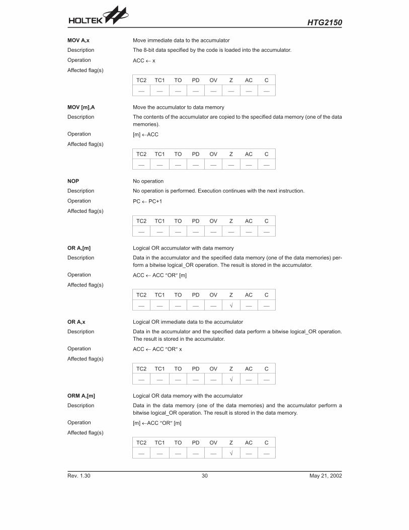
MOV A,x Move immediate data to the accumulator
Description The 8-bit data specified by the code is loaded into the accumulator.
Operation ACC x
Affected flag(s)
TC2 TC1 TO PD OV Z AC C
� � � � � � � �
MOV [m],A Move the accumulator to data memory
Description The contents of the accumulator are copied to the specified data memory (one of the data
memories).
Operation [m] ACC
Affected flag(s)
TC2 TC1 TO PD OV Z AC C
� � � � � � � �
NOP No operation
Description No operation is performed. Execution continues with the next instruction.
Operation PC PC+1
Affected flag(s)
TC2 TC1 TO PD OV Z AC C
� � � � � � � �
OR A,[m] Logical OR accumulator with data memory
Description Data in the accumulator and the specified data memory (one of the data memories) per-
form a bitwise logical_OR operation. The result is stored in the accumulator.
Operation ACC ACC �OR� [m]
Affected flag(s)
TC2 TC1 TO PD OV Z AC C
� � � � � � � �
OR A,x Logical OR immediate data to the accumulator
Description Data in the accumulator and the specified data perform a bitwise logical_OR operation.
The result is stored in the accumulator.
Operation ACC ACC �OR� x
Affected flag(s)
TC2 TC1 TO PD OV Z AC C
� � � � � � � �
ORM A,[m] Logical OR data memory with the accumulator
Description Data in the data memory (one of the data memories) and the accumulator perform a
bitwise logical_OR operation. The result is stored in the data memory.
Operation [m] ACC �OR� [m]
Affected flag(s)
TC2 TC1 TO PD OV Z AC C
� � � � � � � �
HTG2150
Rev. 1.30 30 May 21, 2002
RET Return from subroutine
Description The program counter is restored from the stack. This is a 2-cycle instruction.
Operation PC Stack
Affected flag(s)
TC2 TC1 TO PD OV Z AC C
� � � � � � � �
RET A,x Return and place immediate data in the accumulator
Description The program counter is restored from the stack and the accumulator loaded with the speci-
fied 8-bit immediate data.
Operation PC Stack
ACC x
Affected flag(s)
TC2 TC1 TO PD OV Z AC C
� � � � � � � �
RETI Return from interrupt
Description The program counter is restored from the stack, and interrupts are enabled by setting the
EMI bit. EMI is the enable master (global) interrupt bit.
Operation PC Stack
EMI 1
Affected flag(s)
TC2 TC1 TO PD OV Z AC C
� � � � � � � �
RL [m] Rotate data memory left
Description The contents of the specified data memory are rotated 1 bit left with bit 7 rotated into bit 0.
Operation [m].(i+1) [m].i; [m].i:bit i of the data memory (i=0~6)
[m].0 [m].7
Affected flag(s)
TC2 TC1 TO PD OV Z AC C
� � � � � � � �
RLA [m] Rotate data memory left and place result in the accumulator
Description Data in the specified data memory is rotated 1 bit left with bit 7 rotated into bit 0, leaving the
rotated result in the accumulator. The contents of the data memory remain unchanged.
Operation ACC.(i+1) [m].i; [m].i:bit i of the data memory (i=0~6)
ACC.0 [m].7
Affected flag(s)
TC2 TC1 TO PD OV Z AC C
� � � � � � � �
HTG2150
Rev. 1.30 31 May 21, 2002
RLC [m] Rotate data memory left through carry
Description The contents of the specified data memory and the carry flag are rotated 1 bit left. Bit 7 re-
places the carry bit; the original carry flag is rotated into the bit 0 position.
Operation [m].(i+1) [m].i; [m].i:bit i of the data memory (i=0~6)
[m].0 C
C [m].7
Affected flag(s)
TC2 TC1 TO PD OV Z AC C
� � � � � � � �
RLCA [m] Rotate left through carry and place result in the accumulator
Description Data in the specified data memory and the carry flag are rotated 1 bit left. Bit 7 replaces the
carry bit and the original carry flag is rotated into bit 0 position. The rotated result is stored
in the accumulator but the contents of the data memory remain unchanged.
Operation ACC.(i+1) [m].i; [m].i:bit i of the data memory (i=0~6)
ACC.0 C
C [m].7
Affected flag(s)
TC2 TC1 TO PD OV Z AC C
� � � � � � � �
RR [m] Rotate data memory right
Description The contents of the specified data memory are rotated 1 bit right with bit 0 rotated to bit 7.
Operation [m].i [m].(i+1); [m].i:bit i of the data memory (i=0~6)
[m].7 [m].0
Affected flag(s)
TC2 TC1 TO PD OV Z AC C
� � � � � � � �
RRA [m] Rotate right and place result in the accumulator
Description Data in the specified data memory is rotated 1 bit right with bit 0 rotated into bit 7, leaving
the rotated result in the accumulator. The contents of the data memory remain unchanged.
Operation ACC.(i) [m].(i+1); [m].i:bit i of the data memory (i=0~6)
ACC.7 [m].0
Affected flag(s)
TC2 TC1 TO PD OV Z AC C
� � � � � � � �
RRC [m] Rotate data memory right through carry
Description The contents of the specified data memory and the carry flag are together rotated 1 bit
right. Bit 0 replaces the carry bit; the original carry flag is rotated into the bit 7 position.
Operation [m].i [m].(i+1); [m].i:bit i of the data memory (i=0~6)
[m].7 C
C [m].0
Affected flag(s)
TC2 TC1 TO PD OV Z AC C
� � � � � � � �
HTG2150
Rev. 1.30 32 May 21, 2002

RRCA [m] Rotate right through carry and place result in the accumulator
Description Data of the specified data memory and the carry flag are rotated 1 bit right. Bit 0 replaces
the carry bit and the original carry flag is rotated into the bit 7 position. The rotated result is
stored in the accumulator. The contents of the data memory remain unchanged.
Operation ACC.i [m].(i+1); [m].i:bit i of the data memory (i=0~6)
ACC.7 C
C [m].0
Affected flag(s)
TC2 TC1 TO PD OV Z AC C
� � � � � � � �
SBC A,[m] Subtract data memory and carry from the accumulator
Description The contents of the specified data memory and the complement of the carry flag are sub-
tracted from the accumulator, leaving the result in the accumulator.
Operation ACC ACC+[m]+C
Affected flag(s)
TC2 TC1 TO PD OV Z AC C
� � � � � � � �
SBCM A,[m] Subtract data memory and carry from the accumulator
Description The contents of the specified data memory and the complement of the carry flag are sub-
tracted from the accumulator, leaving the result in the data memory.
Operation [m] ACC+[m]+C
Affected flag(s)
TC2 TC1 TO PD OV Z AC C
� � � � � � � �
SDZ [m] Skip if decrement data memory is 0
Description The contents of the specified data memory are decremented by 1. If the result is 0, the next
instruction is skipped. If the result is 0, the following instruction, fetched during the current
instruction execution, is discarded and a dummy cycle is replaced to get the proper instruc-
tion (2 cycles). Otherwise proceed with the next instruction (1 cycle).
Operation Skip if ([m]�1)=0, [m] ([m]�1)
Affected flag(s)
TC2 TC1 TO PD OV Z AC C
� � � � � � � �
SDZA [m] Decrement data memory and place result in ACC, skip if 0
Description The contents of the specified data memory are decremented by 1. If the result is 0, the next
instruction is skipped. The result is stored in the accumulator but the data memory remains
unchanged. If the result is 0, the following instruction, fetched during the current instruction
execution, is discarded and a dummy cycle is replaced to get the proper instruction (2 cy-
cles). Otherwise proceed with the next instruction (1 cycle).
Operation Skip if ([m]�1)=0, ACC ([m]�1)
Affected flag(s)
TC2 TC1 TO PD OV Z AC C
� � � � � � � �
HTG2150
Rev. 1.30 33 May 21, 2002
SET [m] Set data memory
Description Each bit of the specified data memory is set to 1.
Operation [m] FFH
Affected flag(s)
TC2 TC1 TO PD OV Z AC C
� � � � � � � �
SET [m]. i Set bit of data memory
Description Bit i of the specified data memory is set to 1.
Operation [m].i 1
Affected flag(s)
TC2 TC1 TO PD OV Z AC C
� � � � � � � �
SIZ [m] Skip if increment data memory is 0
Description The contents of the specified data memory are incremented by 1. If the result is 0, the fol-
lowing instruction, fetched during the current instruction execution, is discarded and a
dummy cycle is replaced to get the proper instruction (2 cycles). Otherwise proceed with
the next instruction (1 cycle).
Operation Skip if ([m]+1)=0, [m] ([m]+1)
Affected flag(s)
TC2 TC1 TO PD OV Z AC C
� � � � � � � �
SIZA [m] Increment data memory and place result in ACC, skip if 0
Description The contents of the specified data memory are incremented by 1. If the result is 0, the next
instruction is skipped and the result is stored in the accumulator. The data memory re-
mains unchanged. If the result is 0, the following instruction, fetched during the current in-
struction execution, is discarded and a dummy cycle is replaced to get the proper
instruction (2 cycles). Otherwise proceed with the next instruction (1 cycle).
Operation Skip if ([m]+1)=0, ACC ([m]+1)
Affected flag(s)
TC2 TC1 TO PD OV Z AC C
� � � � � � � �
SNZ [m].i Skip if bit i of the data memory is not 0
Description If bit i of the specified data memory is not 0, the next instruction is skipped. If bit i of the data
memory is not 0, the following instruction, fetched during the current instruction execution,
is discarded and a dummy cycle is replaced to get the proper instruction (2 cycles). Other-
wise proceed with the next instruction (1 cycle).
Operation Skip if [m].i�0
Affected flag(s)
TC2 TC1 TO PD OV Z AC C
� � � � � � � �
HTG2150
Rev. 1.30 34 May 21, 2002

SUB A,[m] Subtract data memory from the accumulator
Description The specified data memory is subtracted from the contents of the accumulator, leaving the
result in the accumulator.
Operation ACC ACC+[m]+1
Affected flag(s)
TC2 TC1 TO PD OV Z AC C
� � � � � � � �
SUBM A,[m] Subtract data memory from the accumulator
Description The specified data memory is subtracted from the contents of the accumulator, leaving the
result in the data memory.
Operation [m] ACC+[m]+1
Affected flag(s)
TC2 TC1 TO PD OV Z AC C
� � � � � � � �
SUB A,x Subtract immediate data from the accumulator
Description The immediate data specified by the code is subtracted from the contents of the accumula-
tor, leaving the result in the accumulator.
Operation ACC ACC+x+1
Affected flag(s)
TC2 TC1 TO PD OV Z AC C
� � � � � � � �
SWAP [m] Swap nibbles within the data memory
Description The low-order and high-order nibbles of the specified data memory (1 of the data memo-
ries) are interchanged.
Operation [m].3~[m].0 � [m].7~[m].4
Affected flag(s)
TC2 TC1 TO PD OV Z AC C
� � � � � � � �
SWAPA [m] Swap data memory and place result in the accumulator
Description The low-order and high-order nibbles of the specified data memory are interchanged, writ-
ing the result to the accumulator. The contents of the data memory remain unchanged.
Operation ACC.3~ACC.0 [m].7~[m].4
ACC.7~ACC.4 [m].3~[m].0
Affected flag(s)
TC2 TC1 TO PD OV Z AC C
� � � � � � � �
HTG2150
Rev. 1.30 35 May 21, 2002
SZ [m] Skip if data memory is 0
Description If the contents of the specified data memory are 0, the following instruction, fetched during
the current instruction execution, is discarded and a dummy cycle is replaced to get the
proper instruction (2 cycles). Otherwise proceed with the next instruction (1 cycle).
Operation Skip if [m]=0
Affected flag(s)
TC2 TC1 TO PD OV Z AC C
� � � � � � � �
SZA [m] Move data memory to ACC, skip if 0
Description The contents of the specified data memory are copied to the accumulator. If the contents is
0, the following instruction, fetched during the current instruction execution, is discarded
and a dummy cycle is replaced to get the proper instruction (2 cycles). Otherwise proceed
with the next instruction (1 cycle).
Operation Skip if [m]=0
Affected flag(s)
TC2 TC1 TO PD OV Z AC C
� � � � � � � �
SZ [m].i Skip if bit i of the data memory is 0
Description If bit i of the specified data memory is 0, the following instruction, fetched during the current
instruction execution, is discarded and a dummy cycle is replaced to get the proper instruc-
tion (2 cycles). Otherwise proceed with the next instruction (1 cycle).
Operation Skip if [m].i=0
Affected flag(s)
TC2 TC1 TO PD OV Z AC C
� � � � � � � �
TABRDC [m] Move the ROM code (current page) to TBLH and data memory
Description The low byte of ROM code (current page) addressed by the table pointer (TBLP) is moved
to the specified data memory and the high byte transferred to TBLH directly.
Operation [m] ROM code (low byte)
TBLH ROM code (high byte)
Affected flag(s)
TC2 TC1 TO PD OV Z AC C
� � � � � � � �
TABRDL [m] Move the ROM code (last page) to TBLH and data memory
Description The low byte of ROM code (last page) addressed by the table pointer (TBLP) is moved to
the data memory and the high byte transferred to TBLH directly.
Operation [m] ROM code (low byte)
TBLH ��� code (high byte)
Affected flag(s)
TC2 TC1 TO PD OV Z AC C
� � � � � � � �
HTG2150
Rev. 1.30 36 May 21, 2002
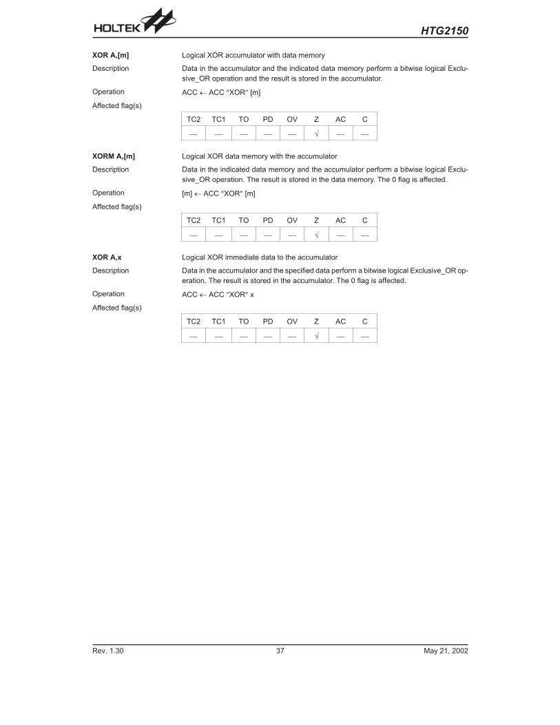
XOR A,[m] Logical XOR accumulator with data memory
Description Data in the accumulator and the indicated data memory perform a bitwise logical Exclu-
sive_OR operation and the result is stored in the accumulator.
Operation ACC ACC �XOR� [m]
Affected flag(s)
TC2 TC1 TO PD OV Z AC C
� � � � � � � �
XORM A,[m] Logical XOR data memory with the accumulator
Description Data in the indicated data memory and the accumulator perform a bitwise logical Exclu-
sive_OR operation. The result is stored in the data memory. The 0 flag is affected.
Operation [m] ACC �XOR� [m]
Affected flag(s)
TC2 TC1 TO PD OV Z AC C
� � � � � � � �
XOR A,x Logical XOR immediate data to the accumulator
Description Data in the accumulator and the specified data perform a bitwise logical Exclusive_OR op-
eration. The result is stored in the accumulator. The 0 flag is affected.
Operation ACC ACC �XOR� x
Affected flag(s)
TC2 TC1 TO PD OV Z AC C
� � � � � � � �
HTG2150
Rev. 1.30 37 May 21, 2002
HTG2150
Rev. 1.30 38 May 21, 2002
Copyright � 2002 by HOLTEK SEMICONDUCTOR INC.
The information appearing in this Data Sheet is believed to be accurate at the time of publication. However, Holtek as-sumes no responsibility arising from the use of the specifications described. The applications mentioned herein are usedsolely for the purpose of illustration and Holtek makes no warranty or representation that such applications will be suitablewithout further modification, nor recommends the use of its products for application that may present a risk to human life
due to malfunction or otherwise. Holtek�s products are not authorized for use as critical components in life support devicesor systems. Holtek reserves the right to alter its products without prior notification. For the most up-to-date information,please visit our web site at http://www.holtek.com.tw.
Holtek Semiconductor Inc. (Headquarters)No.3, Creation Rd. II, Science Park, Hsinchu, TaiwanTel: 886-3-563-1999Fax: 886-3-563-1189http://www.holtek.com.tw
Holtek Semiconductor Inc. (Taipei Sales Office)4F-2, No. 3-2, YuanQu St., Nankang Software Park, Taipei 115, TaiwanTel: 886-2-2655-7070Fax: 886-2-2655-7373Fax: 886-2-2655-7383 (International sales hotline)
Holtek Semiconductor Inc. (Shanghai Sales Office)7th Floor, Building 2, No.889, Yi Shan Rd., Shanghai, China 200233Tel: 021-6485-5560Fax: 021-6485-0313http://www.holtek.com.cn
Holtek Semiconductor Inc. (Shenzhen Sales Office)43F, SEG Plaza, Shen Nan Zhong Road, Shenzhen, China 518031Tel: 0755-8346-5589Fax: 0755-8346-5590ISDN: 0755-8346-5591
Holtek Semiconductor Inc. (Beijing Sales Office)Suite 1721, Jinyu Tower, A129 West Xuan Wu Men Street, Xicheng District, Beijing, China 100031Tel: 010-6641-0030, 6641-7751, 6641-7752Fax: 010-6641-0125
Holmate Semiconductor, Inc. (North America Sales Office)46712 Fremont Blvd., Fremont, CA 94538Tel: 510-252-9880Fax: 510-252-9885http://www.holmate.com
Related Documents