Taranjit Kukal Zhen Mu Ph.D Cadence Design Systems MemCon 2015 How to Efficiently Analyze a DDR4 Interface

Welcome message from author
This document is posted to help you gain knowledge. Please leave a comment to let me know what you think about it! Share it to your friends and learn new things together.
Transcript
Taranjit Kukal
Zhen Mu Ph.D
Cadence Design Systems
MemCon 2015
How to Efficiently Analyze a DDR4 Interface
2 © 2015 Cadence Design Systems, Inc. All rights reserved.
• Power-aware signal integrity (SI) in memory bus design and analysis
• Modeling methodology for integrated core and power-aware parallel bus system with Cadence-Sigrity tools
• Building an integrated core and power-aware parallel bus system in Cadence-Sigrity tool environment
• Case study – A virtual reference design based on the Cadence DDR4 IP test chip,
package, and PCB
– Simulation and measurement correlation
Agenda

3 © 2015 Cadence Design Systems, Inc. All rights reserved.
Parallel Bus Analysis at System Level
4 © 2015 Cadence Design Systems, Inc. All rights reserved.
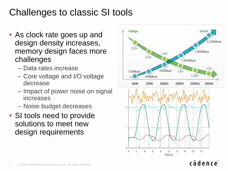
• As clock rate goes up and design density increases, memory design faces more challenges– Data rates increase
– Core voltage and I/O voltage decrease
– Impact of power noise on signal increases
– Noise budget decreases
• SI tools need to provide solutions to meet new design requirements
Challenges to classic SI tools
5 © 2015 Cadence Design Systems, Inc. All rights reserved.
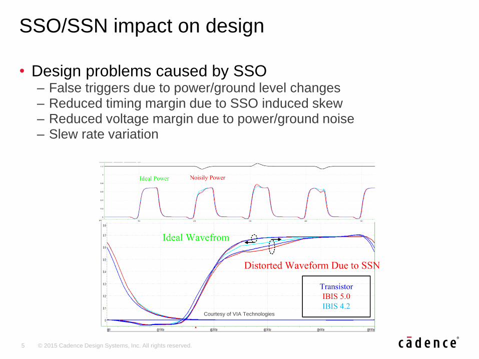
• Design problems caused by SSO– False triggers due to power/ground level changes– Reduced timing margin due to SSO induced skew – Reduced voltage margin due to power/ground noise – Slew rate variation
SSO/SSN impact on design
Courtesy of VIA Technologies

6 © 2015 Cadence Design Systems, Inc. All rights reserved.
• Increasing data rates
• Shrinking design margin
• Decreasing power
• Introducing serial link design methodologies– JEDEC standard specifies
BER for data signals
• Design and analysis need to consider core and system at the same time
DDR4 technology demands
7 © 2015 Cadence Design Systems, Inc. All rights reserved.
Modeling methodology for integrated core and power aware parallel bus system with Cadence-Sigrity tools
© 2015 Cadence Design Systems, Inc. All rights reserved worldwide. Cadence and the Cadence logo are
registered trademarks and Sigrity is a trademark of Cadence Design Systems.
8 © 2015 Cadence Design Systems, Inc. All rights reserved.
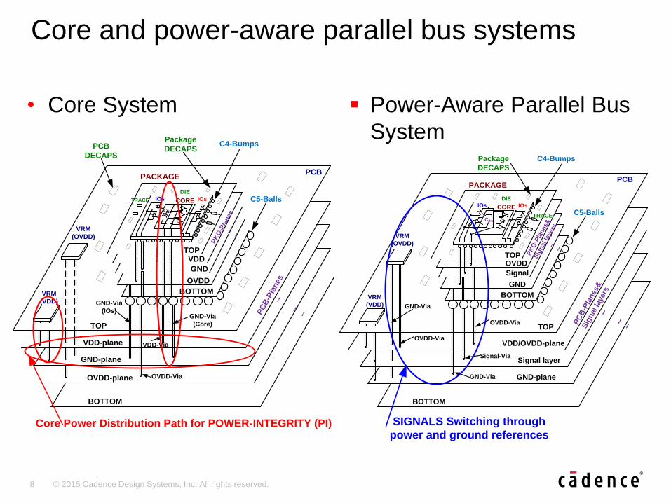
Core and power-aware parallel bus systems
• Core System Power-Aware Parallel Bus
System
VDD-plane
GND-plane
OVDD-plane
TOP
BOTTOM
VDD
GND
OVDD
TOP
BOTTOM
PACKAGE
DIE
PCB
GND-Via
(Core)
GND-Via
(IOs)
OVDD-Via
VDD-Via
Cdie
IOs CORE IOs TRACE
VRM
(VDD)
VRM
(OVDD)
PCB
DECAPS
Package
DECAPS
PC
B-P
lanes
--
----
PK
G-P
lanes
----
C5-Balls
C4-Bumps
Core Power Distribution Path for POWER-INTEGRITY (PI)
Signal layer
GND-plane
VDD/OVDD-plane
TOP
BOTTOM
Signal
GND
OVDD TOP
BOTTOM
PACKAGE
DIE
PCB
GND-Via
OVDD-Via
Cdie
IOs CORE IOs
TRACE
VRM
(VDD)
VRM
(OVDD)
Package
DECAPS
PC
B-P
lanes&
Sig
nal la
yers
--
----
PK
G-P
lanes&
Sig
nal la
yers
----
C5-Balls
C4-Bumps
Signal-Via
OVDD-Via
GND-Via
SIGNALS Switching through
power and ground references

9 © 2015 Cadence Design Systems, Inc. All rights reserved.
Power-aware parallel bus
• PCB parallel bus consists of data and strobe signal nets and
power distribution network (PDN)
• PDNs consists of PWR and GND planes of PCB (packages)
1st-byte lane of
• DATA (DQ<0>-DQ<7>) and
• STROBE (DQS_N<0> & DQS_P<0>)
2nd-byte lane of
• DATA (DQ<8>-DQ<15>) and
• STROBE (DQS_N<1> & DQS_P<1>)

10 © 2015 Cadence Design Systems, Inc. All rights reserved.
Cadence IO SSO Chip-PKG-PCB Co-Simulation
Including Chip IO
Interconnect Model
Input
BufferRX
Main
Buffer
VSS
VDD_IO
Main
Buffer
Receiv
er
VRM
Main
Buffer
Input
Buffer
Driv
er
Chip Package PCB
107mV

11 © 2015 Cadence Design Systems, Inc. All rights reserved.
Core-system model
• Rgrid, Cchip values and current profile are critical for
optimizing power integrity performance of Core-PDN
• Minimizing transient voltage drop at the core is critical to
guarantee the specified core-operating frequency
Core-VRM-ModelIC-Package Model
Rgrid
Cchip
ImuP
Core-Model PCB Model
Vdd
Rr
Cd
Rd
Lr
+
-
Cb
Rb
Lb
Rcore_2Rcore_1 Lcore_1 Lcore_2
Norton
Equivalent
Circuit
R-L-C model
from XtractIM
for
IC-Package
Core-PDN,
w/wo
Package
DECAPS
S-parameter
model from
PowerSI
for PCB
Core-PDN,
With PCB
DECAPS
Behavioral from the
output impedance
characteristic
12 © 2015 Cadence Design Systems, Inc. All rights reserved.
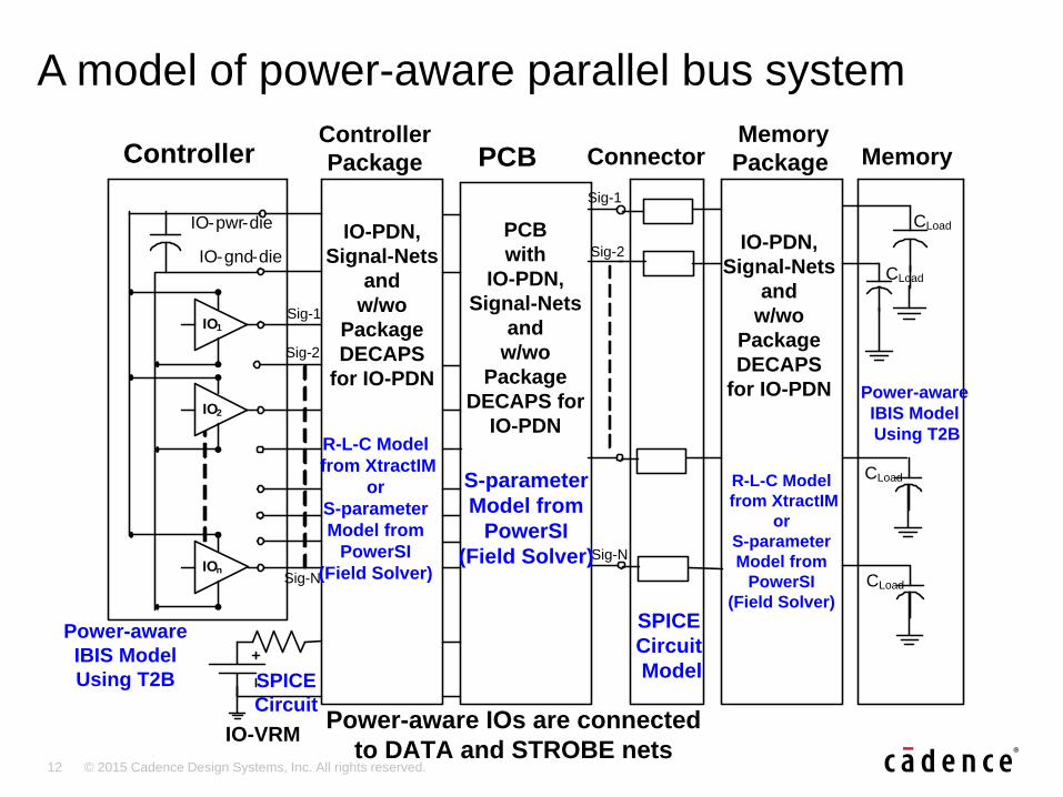
A model of power-aware parallel bus system
PCB
with
IO-PDN,
Signal-Nets
and
w/wo
Package
DECAPS for
IO-PDN
IO-pwr-die
Sig-1
IO-gnd-die
Sig-2
Sig-N
IO1
IO2
IOn
Sig-2
Sig-1
CLoad
CLoad
CLoad
Sig-N
CLoad
IO-PDN,
Signal-Nets
and
w/wo
Package
DECAPS
for IO-PDN
IO-PDN,
Signal-Nets
and
w/wo
Package
DECAPS
for IO-PDN
Controller
Controller
Package PCB Connector Memory
Package Memory
Power-aware
IBIS Model
Using T2B SPICE
Circuit
IO-VRM
R-L-C Model
from XtractIM
or
S-parameter
Model from
PowerSI
(Field Solver)
S-parameter
Model from
PowerSI
(Field Solver)
SPICE
Circuit
Model
R-L-C Model
from XtractIM
or
S-parameter
Model from
PowerSI
(Field Solver)
Power-aware
IBIS Model
Using T2B
Power-aware IOs are connected
to DATA and STROBE nets

13 © 2015 Cadence Design Systems, Inc. All rights reserved.
Integrated core and power-aware parallel bus system
Core-Model VRM-Model
Core-System
Model
Package PCB
PCB
with
IO-PDN,
Signal-Nets
and
w/wo
Package
DECAPS for
IO-PDN
IO-pwr-die
Sig-1
IO-gnd-die
Sig-2
Sig-N
IO1
IO2
IOn
Sig-2
Sig-1
Power-aware IOs are connected
to DATA and STROBE nets
CLoad
CLoad
CLoad
Sig-N
CLoad
IO-PDN,
Signal-Nets
and
w/wo
Package
DECAPS
for IO-PDN
Rgrid
Cchip
ImuP
Vdd
Rr
Cd
Rd
Cb
Rb
Lb
+
- Core-PDN
Rt1
Rt2 Vt
Rt1
Rt2 Vt
Rt1
Rt2 Vt
Rt1
Rt2 Vt
Controller DIMM Routing Memory Termination
SPICE
Circuit
Model
SPICE
Circuit
Model
SPICE
Circuit
Model
SPICE
Circuit
Model
SPICE
Circuit
Model
Power-aware
IBIS Model
Using T2BPower-aware
IBIS Model
Using T2B
R-L-C Model
from XtractIM
or
S-parameter
Model from
PowerSI
(Field Solver)
S-parameter
Model from
PowerSI
(Field Solver)
IO-VRM
Model of
power-
aware
parallel bus
14 © 2015 Cadence Design Systems, Inc. All rights reserved.
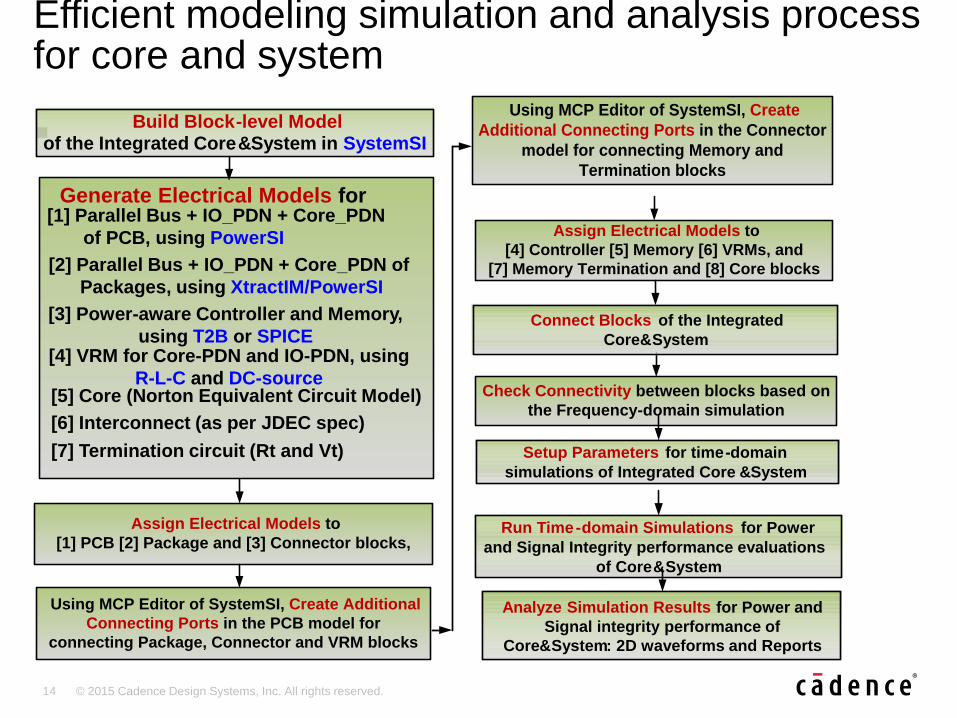
Efficient modeling simulation and analysis process for core and system
. Using MCP Editor of SystemSI, Create
Additional Connecting Ports in the Connector
model for connecting Memory and
Termination blocks
Generate Electrical Models for [1] Parallel Bus + IO_PDN + Core_PDN
of PCB, using PowerSI
[2] Parallel Bus + IO_PDN + Core_PDN of
Packages, using XtractIM/PowerSI
[3] Power-aware Controller and Memory,
using T2B or SPICE[4] VRM for Core-PDN and IO-PDN, using
R-L-C and DC-source[5] Core (Norton Equivalent Circuit Model)
[6] Interconnect (as per JDEC spec)
[7] Termination circuit (Rt and Vt)
Assign Electrical Models to
[1] PCB [2] Package and [3] Connector blocks,
Using MCP Editor of SystemSI, Create Additional
Connecting Ports in the PCB model for
connecting Package, Connector and VRM blocks
Assign Electrical Models to
[4] Controller [5] Memory [6] VRMs, and
[7] Memory Termination and [8] Core blocks
Check Connectivity between blocks based on
the Frequency-domain simulation
Build Block-level Model of the Integrated Core&System in SystemSI
Connect Blocks of the Integrated
Core&System
Setup Parameters for time-domain
simulations of Integrated Core &System
Run Time-domain Simulations for Power
and Signal Integrity performance evaluations
of Core&System
Analyze Simulation Results for Power and
Signal integrity performance of
Core&System: 2D waveforms and Reports
15 © 2015 Cadence Design Systems, Inc. All rights reserved.
Building an integrated core and power aware parallel bus system
© 2015 Cadence Design Systems, Inc. All rights reserved worldwide. Cadence and the Cadence logo are
registered trademarks and Sigrity and SPEED2000 are trademarks of Cadence Design Systems.
16 © 2015 Cadence Design Systems, Inc. All rights reserved.
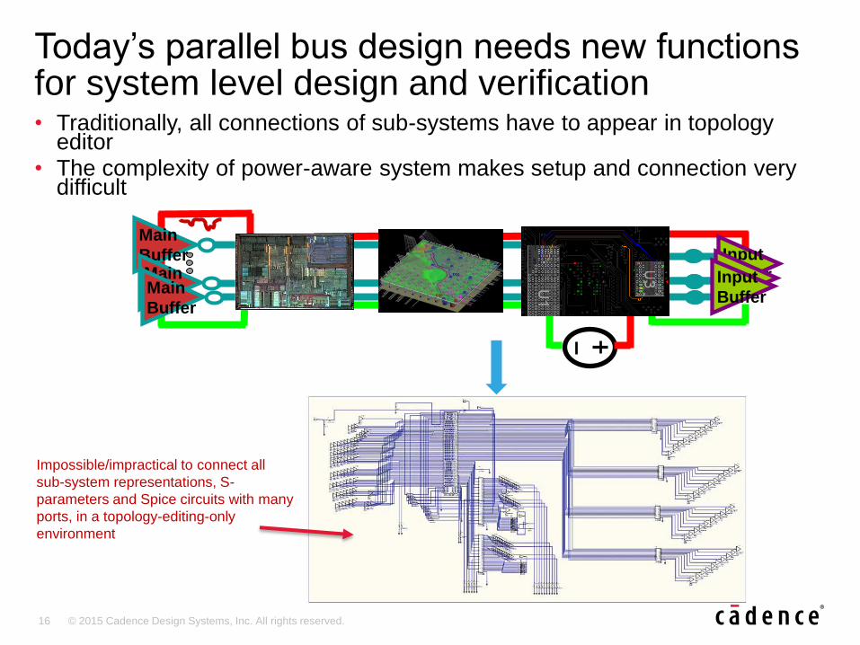
• Traditionally, all connections of sub-systems have to appear in topology editor
• The complexity of power-aware system makes setup and connection very difficult
Today’s parallel bus design needs new functions for system level design and verification
Input
BufferRX
Main
BufferMain
BufferMain
Buffer
Input
Buffer
Impossible/impractical to connect all
sub-system representations, S-
parameters and Spice circuits with many
ports, in a topology-editing-only
environment
17 © 2015 Cadence Design Systems, Inc. All rights reserved.
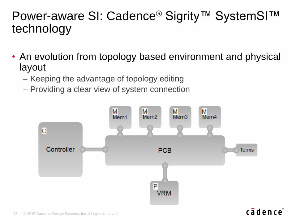
• An evolution from topology based environment and physical layout– Keeping the advantage of topology editing
– Providing a clear view of system connection
Power-aware SI: Cadence® Sigrity™ SystemSI™ technology
18 © 2015 Cadence Design Systems, Inc. All rights reserved.
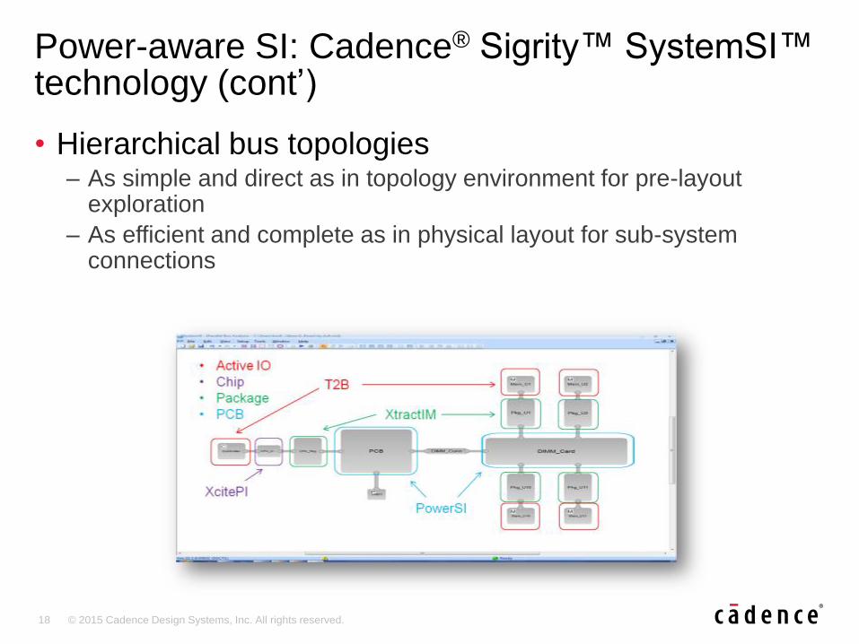
• Hierarchical bus topologies– As simple and direct as in topology environment for pre-layout
exploration
– As efficient and complete as in physical layout for sub-system connections
Power-aware SI: Cadence® Sigrity™ SystemSI™ technology (cont’)
19 © 2015 Cadence Design Systems, Inc. All rights reserved.
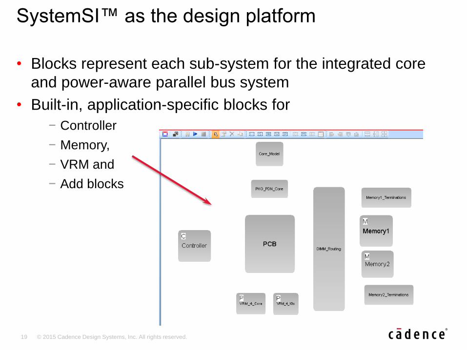
SystemSI™ as the design platform
• Blocks represent each sub-system for the integrated core
and power-aware parallel bus system
• Built-in, application-specific blocks for
− Controller
− Memory,
− VRM and
− Add blocks

20 © 2015 Cadence Design Systems, Inc. All rights reserved.
XcitePI™
XtractIM™
PowerSI™
T2B™
PowerSI™Electrical model generation
T2B™
21 © 2015 Cadence Design Systems, Inc. All rights reserved.
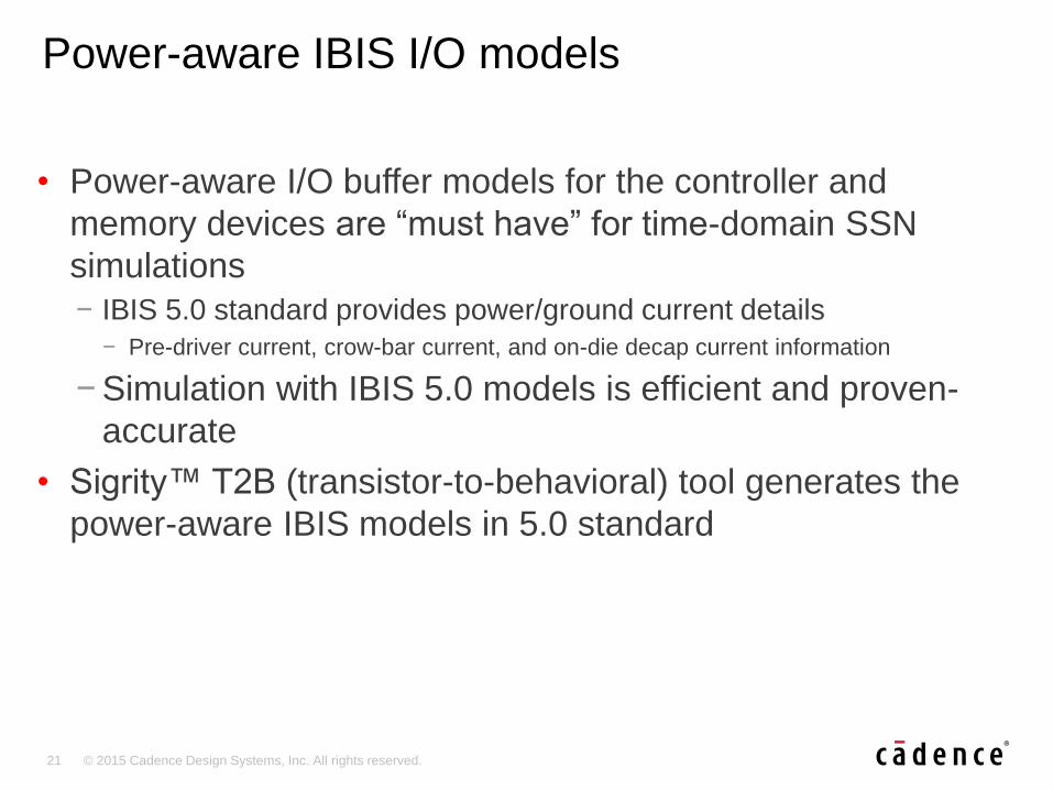
Power-aware IBIS I/O models
• Power-aware I/O buffer models for the controller and
memory devices are “must have” for time-domain SSN
simulations
− IBIS 5.0 standard provides power/ground current details
− Pre-driver current, crow-bar current, and on-die decap current information
− Simulation with IBIS 5.0 models is efficient and proven-
accurate
• Sigrity™ T2B (transistor-to-behavioral) tool generates the
power-aware IBIS models in 5.0 standard
22 © 2015 Cadence Design Systems, Inc. All rights reserved.
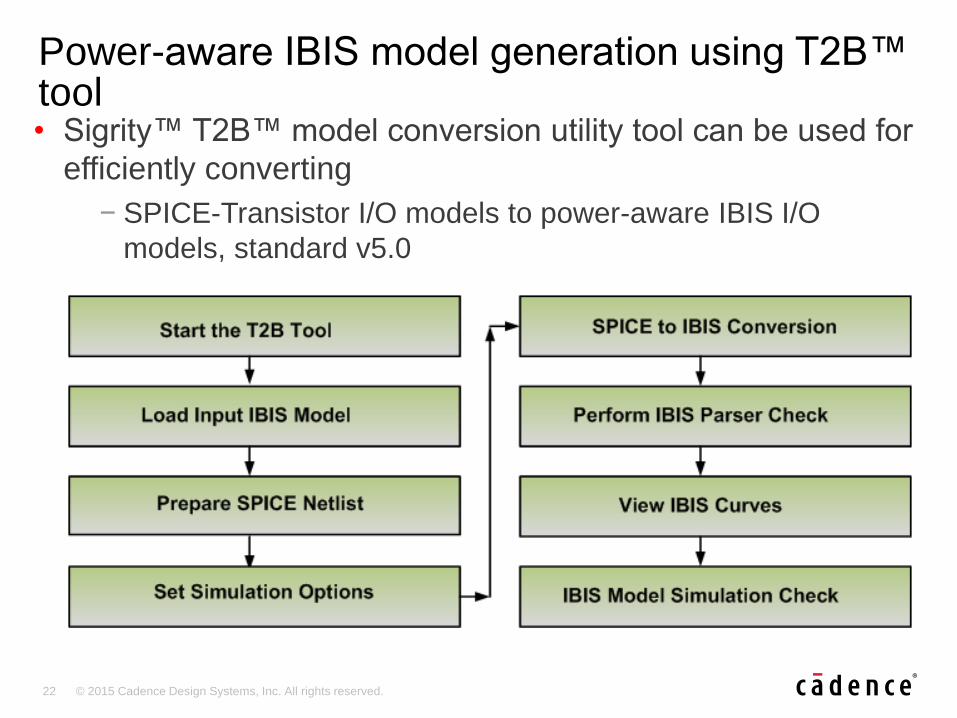
Power-aware IBIS model generation using T2B™tool• Sigrity™ T2B™ model conversion utility tool can be used for
efficiently converting
− SPICE-Transistor I/O models to power-aware IBIS I/O
models, standard v5.0
23 © 2015 Cadence Design Systems, Inc. All rights reserved.
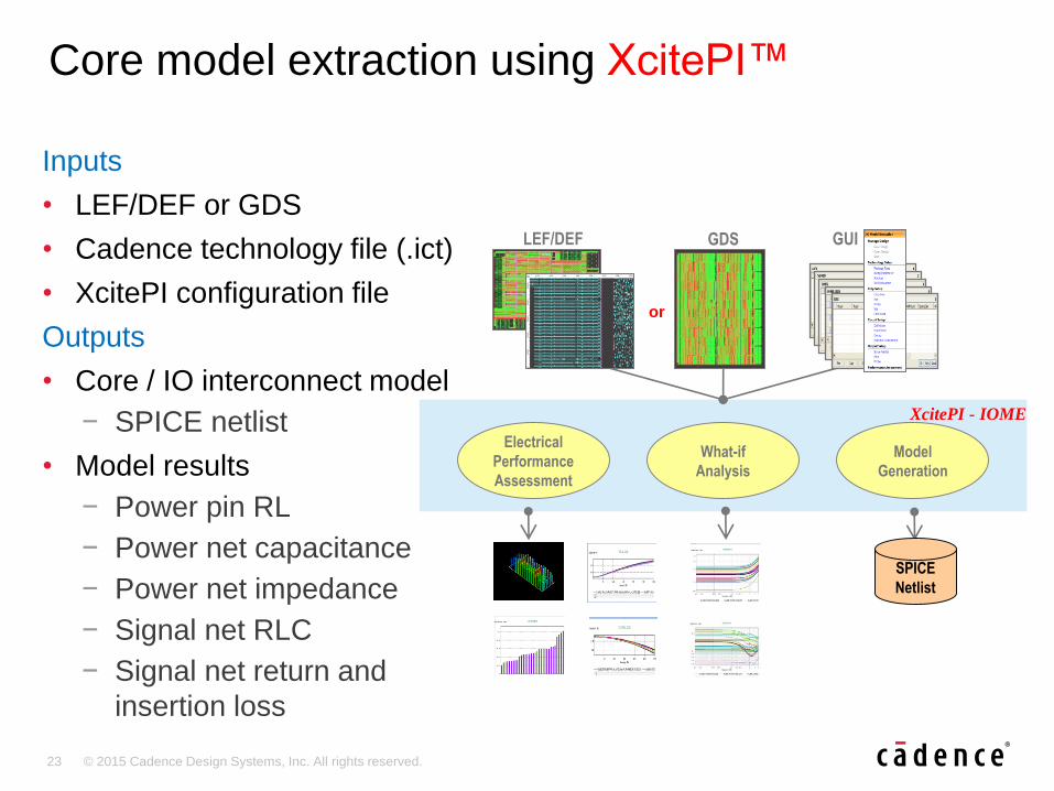
Core model extraction using XcitePI™
Inputs
• LEF/DEF or GDS
• Cadence technology file (.ict)
• XcitePI configuration file
Outputs
• Core / IO interconnect model
− SPICE netlist
• Model results
− Power pin RL
− Power net capacitance
− Power net impedance
− Signal net RLC
− Signal net return and
insertion loss
Electrical
Performance
Assessment
What-if
Analysis
Model
Generation
LEF/DEF GDS GUI
XcitePI - IOME
SPICE
Netlist
or
24 © 2015 Cadence Design Systems, Inc. All rights reserved.
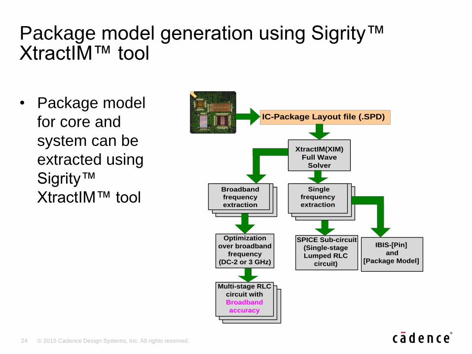
Package model generation using Sigrity™XtractIM™ tool
IC-Package Layout file (.SPD)
XtractIM(XIM)
Full Wave
Solver
Single
frequency
extraction
Broadband
frequency
extraction
Optimization
over broadband
frequency
(DC-2 or 3 GHz)
SPICE Sub-circuit
(Single-stage
Lumped RLC
circuit)
IBIS-[Pin]
and
[Package Model]
Multi-stage RLC
circuit with
Broadband
accuracy
• Package model
for core and
system can be
extracted using
Sigrity™
XtractIM™ tool
25 © 2015 Cadence Design Systems, Inc. All rights reserved.
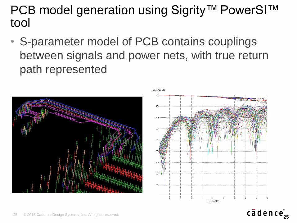
PCB model generation using Sigrity™ PowerSI™ tool
• S-parameter model of PCB contains couplings
between signals and power nets, with true return
path represented
25

26 © 2015 Cadence Design Systems, Inc. All rights reserved.
Connecting blocks in SystemSI™
• Blocks of core and power-aware parallel bus system are
connected through MCP (Model Connection Protocol)
27 © 2015 Cadence Design Systems, Inc. All rights reserved.
Solution demonstration: An LPDDR4 design
© 2015 Cadence Design Systems, Inc. All rights reserved worldwide. Cadence and the Cadence logo are
registered trademarks and Sigrity is a trademark of Cadence Design Systems.
28 © 2015 Cadence Design Systems, Inc. All rights reserved.
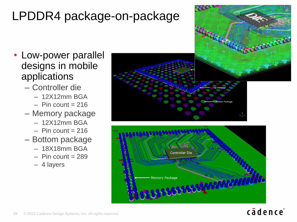
LPDDR4 package-on-package
• Low-power parallel designs in mobile applications– Controller die
– 12X12mm BGA
– Pin count = 216
– Memory package– 12X12mm BGA
– Pin count = 216
– Bottom package– 18X18mm BGA
– Pin count = 289
– 4 layers

29 © 2015 Cadence Design Systems, Inc. All rights reserved.
Package design in Allegro Package Designer
© 2015 Cadence Design Systems, Inc. All rights reserved worldwide. Cadence, the Cadence logo, and
Allegro are registered trademarks of Cadence Design Systems.
30 © 2015 Cadence Design Systems, Inc. All rights reserved.
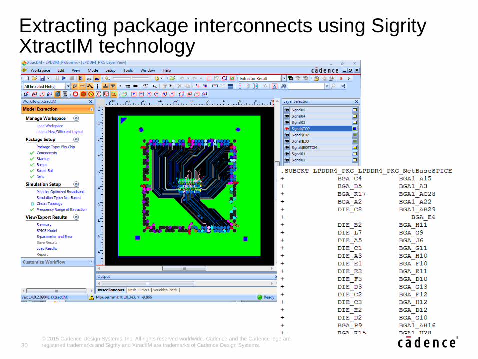
Extracting package interconnects using Sigrity XtractIM technology
© 2015 Cadence Design Systems, Inc. All rights reserved worldwide. Cadence and the Cadence logo are
registered trademarks and Sigrity and XtractIM are trademarks of Cadence Design Systems.

31 © 2015 Cadence Design Systems, Inc. All rights reserved.
Simulating LPDDR4 design using Sigrity SystemSI technology
Building block topology
Defining bus groups
Setting up timing budget
© 2015 Cadence Design Systems, Inc. All rights reserved worldwide. Cadence and the Cadence logo are
registered trademarks and Sigrity and SystemSI are trademarks of Cadence Design Systems.
32 © 2015 Cadence Design Systems, Inc. All rights reserved.
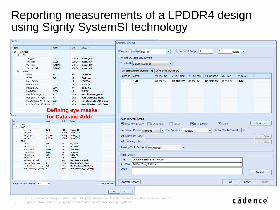
Reporting measurements of a LPDDR4 design using Sigrity SystemSI technology
Generating measurement report
Defining eye masks
for Data and Addr
© 2015 Cadence Design Systems, Inc. All rights reserved worldwide. Cadence and the Cadence logo are
registered trademarks and Sigrity is a trademark of Cadence Design Systems.
33 © 2015 Cadence Design Systems, Inc. All rights reserved.
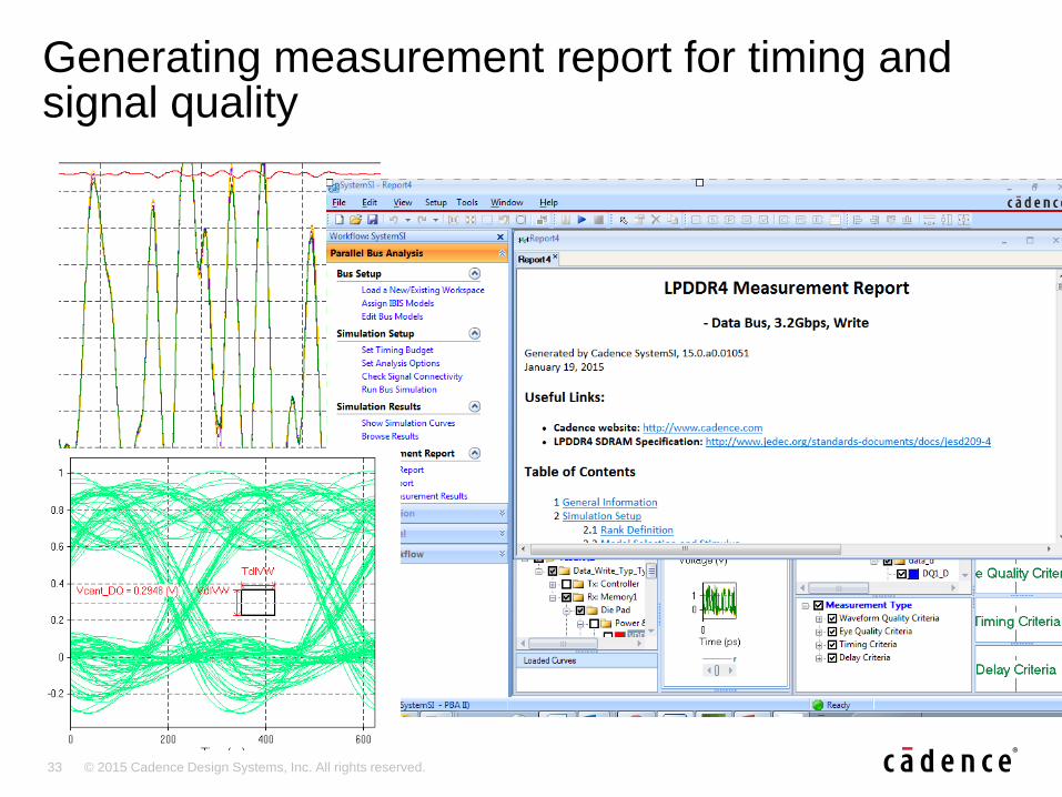
Generating measurement report for timing and signal quality

34 © 2015 Cadence Design Systems, Inc. All rights reserved.
Signal quality reported by simulating the design with channel analysis option
35 © 2015 Cadence Design Systems, Inc. All rights reserved.
Case study: Simulation and measurement correlation of a DDR4 design
© 2015 Cadence Design Systems, Inc. All rights reserved worldwide. Cadence and the Cadence logo are
registered trademarks and Sigrity is a trademark of Cadence Design Systems.
36 © 2015 Cadence Design Systems, Inc. All rights reserved.
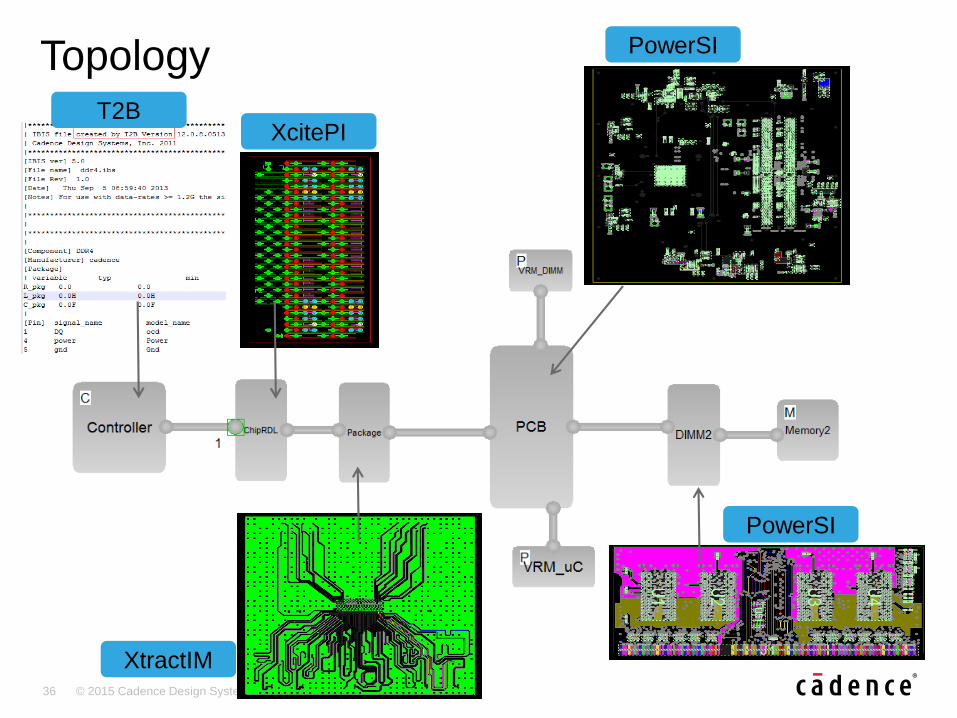
Topology
XcitePI
XtractIM
PowerSI
T2B
PowerSI

37 © 2015 Cadence Design Systems, Inc. All rights reserved.
Stimulus settings
38 © 2015 Cadence Design Systems, Inc. All rights reserved.
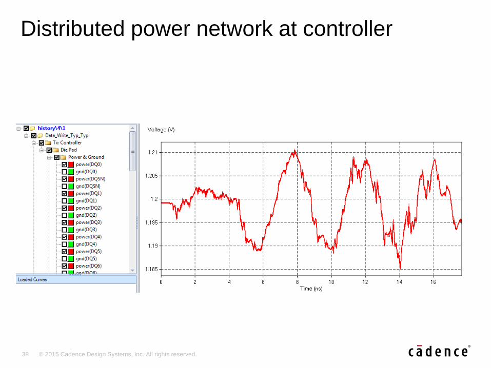
Distributed power network at controller
39 © 2015 Cadence Design Systems, Inc. All rights reserved.
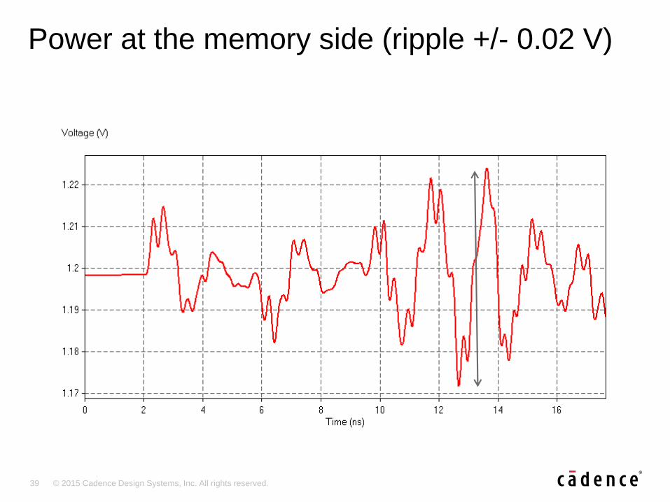
Power at the memory side (ripple +/- 0.02 V)

40 © 2015 Cadence Design Systems, Inc. All rights reserved.
Eye height measurementEye
HeightMean
Sim Results 556 mV
H/W Results 526 mV
Peak to peak 0.8 V
Peak to peak 0.8 V
41 © 2015 Cadence Design Systems, Inc. All rights reserved.
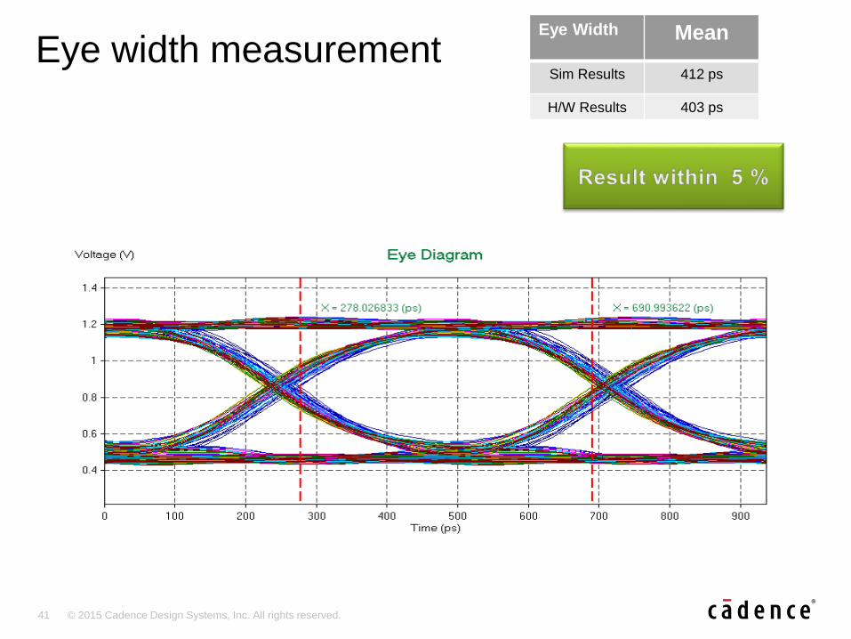
Eye width measurementEye Width Mean
Sim Results 412 ps
H/W Results 403 ps
44 © 2015 Cadence Design Systems, Inc. All rights reserved.
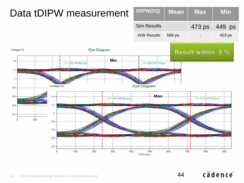
Data tDIPW measurement
44
tDIPW(DQ) Mean Max Min
Sim Results 473 ps 449 ps
H/W Results 586 ps - 453 ps
45 © 2015 Cadence Design Systems, Inc. All rights reserved.
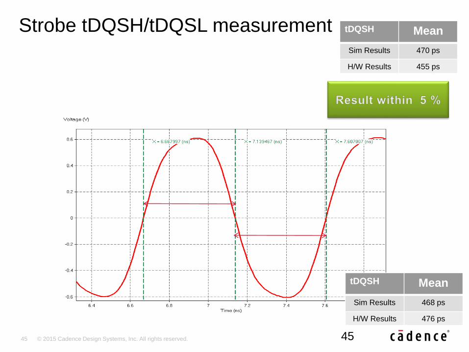
Strobe tDQSH/tDQSL measurement
45
tDQSH Mean
Sim Results 470 ps
H/W Results 455 ps
tDQSH Mean
Sim Results 468 ps
H/W Results 476 ps
46 © 2015 Cadence Design Systems, Inc. All rights reserved.
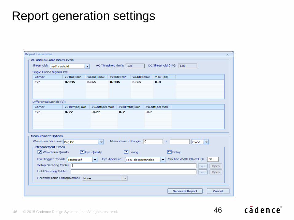
Report generation settings
46
47 © 2015 Cadence Design Systems, Inc. All rights reserved.
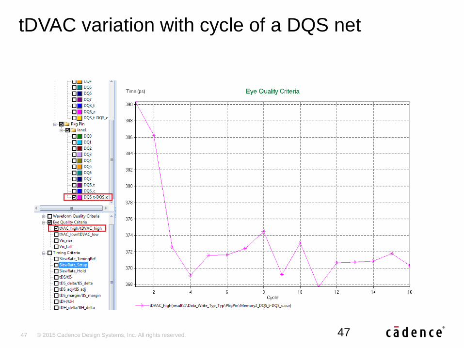
tDVAC variation with cycle of a DQS net
47

48 © 2015 Cadence Design Systems, Inc. All rights reserved.
tDVAC Strobe report
48
tDVAC Mean Max Min
Sim Results 367 ps 360 ps
H/W Results 347 ps 382.7 ps 343.10 ps
49 © 2015 Cadence Design Systems, Inc. All rights reserved.
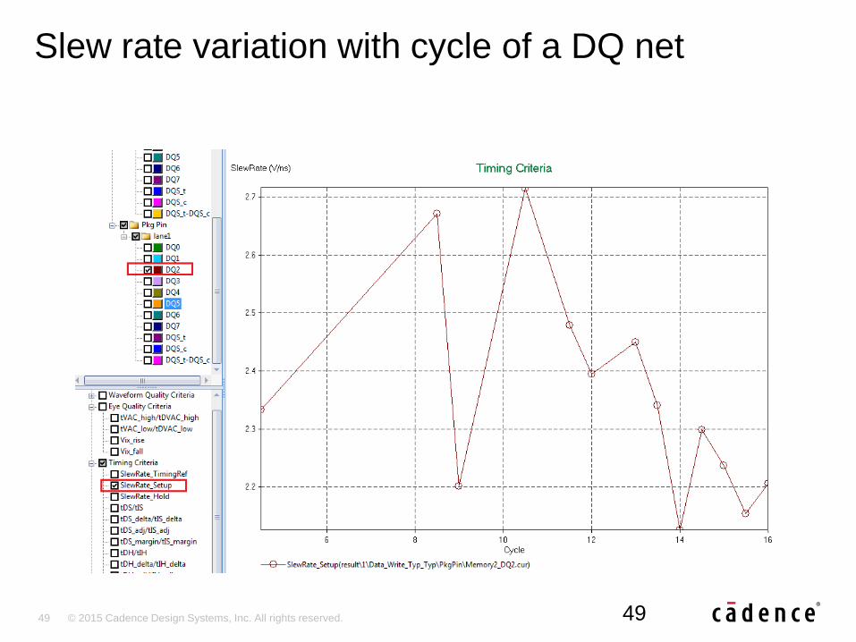
Slew rate variation with cycle of a DQ net
49
50 © 2015 Cadence Design Systems, Inc. All rights reserved.
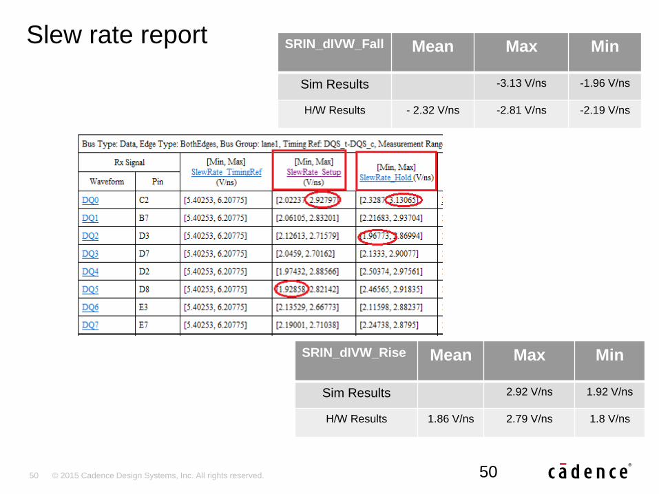
Slew rate report
50
SRIN_dIVW_Fall Mean Max Min
Sim Results -3.13 V/ns -1.96 V/ns
H/W Results - 2.32 V/ns -2.81 V/ns -2.19 V/ns
SRIN_dIVW_Rise Mean Max Min
Sim Results 2.92 V/ns 1.92 V/ns
H/W Results 1.86 V/ns 2.79 V/ns 1.8 V/ns
51 © 2015 Cadence Design Systems, Inc. All rights reserved.
Summary
52 © 2015 Cadence Design Systems, Inc. All rights reserved.
• DDR4 and LPDDR4 technologies pose new challenges to parallel bus design and analysis– Serial link design methods introduced to the design specification
– Lower power assumption requires dedicated margin tuning
• Combination of power-aware SI simulation and channel simulation is the only way to support these new technologies
• Cadence Sigrity™ technology provides comprehensive system level SI/PI solutions for core, package, and PCB– Unique methodology of power-aware simulation for core and parallel
bus system
– Behavioral model (Chip and core power) generation and simulation
– Package and board model extraction
– Integration of patented channel simulation approach in parallel bus analysis flow
Conclusion
© 2015 Cadence Design Systems, Inc. All rights reserved worldwide. Cadence, the Cadence logo, and Allegro are
registered trademarks and Sigrity, SystemSI, and XtractIM are trademarks of Cadence Design Systems. All other
trademarks are the property of their respective owners.
Related Documents