ELEC3342: Digital System Designs First Semester, 2021–22 Homework 2 (r1.0) Due: • Part (A) -- 10 Nov, 2021, 11:59pm • Part (B) -- 10 Nov, 2021, 11:59pm Instruction: Submit your answers electronically through Moodle. There are 2 major parts in this homework. Part A includes questions that aim to help you with under- standing the lecture materials. They resemble the kind of questions you will encounter in quizzes and the final exam. Some of these questions may also ask you to implement and test small designs in VHDL. This part of homework must be completed individually. Part B of this homework contains a mini-project that you should work in groups of 2. Your submitted work will be graded by an auto tester and therefore you should make sure your submitted files conform to the required format. The following summarizes the 2 parts. Part Type Indv/Grp A Basic problem set Individual B Mini-project Group of 4 In all cases, you are encouraged to discuss the homework problems offline or online using Piazza. However, you should not ask for or give out solution directly as that defeat the idea of having homework exercise. Giving out answers or copying answers directly will likely constitute an act of plagiarism, which is a serious offence.

Welcome message from author
This document is posted to help you gain knowledge. Please leave a comment to let me know what you think about it! Share it to your friends and learn new things together.
Transcript

ELEC3342: Digital System Designs
First Semester, 2021–22
Homework2 (r1.0)
Due:
• Part (A) -- 10 Nov, 2021, 11:59pm
• Part (B) -- 10 Nov, 2021, 11:59pm
Instruction: Submit your answers electronically through Moodle.
There are 2 major parts in this homework. Part A includes questions that aim to help you with under-standing the lecture materials. They resemble the kind of questions you will encounter in quizzes andthe final exam. Some of these questions may also ask you to implement and test small designs in VHDL.This part of homework must be completed individually.
Part B of this homework contains a mini-project that you should work in groups of 2. Your submittedwork will be graded by an auto tester and therefore you should make sure your submitted files conformto the required format.
The following summarizes the 2 parts.
Part Type Indv/Grp
A Basic problem set IndividualB Mini-project Group of 4
In all cases, you are encouraged to discuss the homework problems offline or online using Piazza. However,you should not ask for or give out solution directly as that defeat the idea of having homework exercise.Giving out answers or copying answers directly will likely constitute an act of plagiarism, which is aserious offence.

Part A: Problem Set
A.1
The circuit shown in Figure A.1 implements an FSM. Draw the state transition diagram of this FSM,and describe in words what is its function.
A
YD Q
RCLK
D Q
RCLK
CLKRESET
Figure A.1: Circuit for an FSM
A.2 Gray Code Counter
Gray codes have the useful property that consecutive number representations only differ in exactly oneposition. Your job is to design a gray code counter in this question. A 3-bit Gray code representing thenumbers 0 to 7 is shown below:
Number Gray Code
0 0 0 01 0 0 12 0 1 13 0 1 04 1 1 05 1 1 16 1 0 17 1 0 0
Design a 3-bit modulo 8 Gray code counter with a synchronous reset using VHDL. At reset, the outputshould be the number 0 (000). The counter wraps back to 0 after counting to 7 (100). On each clockedge, the output should advance to the next Gray code, except when a special rest R is asserted. WhenR is asserted, the counter resets to 000 on the next cycle. Submit your VHDL file as graycnt.vhd. Alsosubmit a short answer to this question describing your circuit.
r1.0 Page 2 of 11

ELEC3342: Digital System Designs Homework 2, Part A
A.3 Loadable Left-Right Shift Register
In class, we showed a standard shift register that shift data to the right. In this question, you will designa 4-bit shift register that can shift the data in the register either to the left or to the right. Specifically,your circuit should include the following input and output signals:
Name Direction Description
s input serial input from leftt input serial input from rightdir input 0: shift right ; 1: shift leftd[3:0] input value to be loadedv[3:0] output values stored in the shift registerload input 1: parallel load value d; 0: otherwiseen input 1: normal operation; 0: output v unchangedclk input Clock input
During normal operation (en=1), the following operation is expected:
• if load=1, then v ← d after positive clock edge.
• if load=0, then the circuit shift data as follows:
– RIGHT: v[n-1] ← s and v[i] ← v[i+1] for i = {n− 2, . . . , 0} after positive clock edge.
– LEFT: v[0] ← t and v[i] ← v[i-1] for i = {n− 1, . . . , 1} after positive clock edge.
Design your circuit using building blocks that we have described in class (e.g. DFF, muxes, gates, adders,counters, etc). Submit a short answer that include the top-level schematics of the circuit and describehow it works.
r1.0 Page 3 of 11
ELEC3342: Digital System Designs Homework 2, Part A
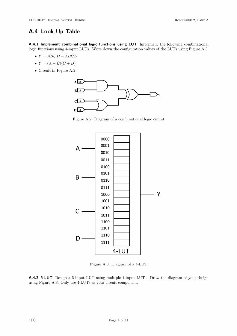
A.4 Look Up Table
A.4.1 Implement combinational logic functions using LUT Implement the following combinationallogic functions using 4-input LUTs. Write down the configuration values of the LUTs using Figure A.3.
• Y = ABCD +ABCD
• Y = (A+ B)(C +D)
• Circuit in Figure A.2
10/25/21, 6:58 PM lut3.svg
file:///Users/gyz/Documents/course/elec3342/hw/lut3.svg 1/1
x1B
x1A
x1D
x1C
x1 Y
Figure A.2: Diagram of a combinational logic circuit
4-LUT
00000001
0010
0011
01000101
0110
011110001001
1010
101111001101
1110
1111
A
B
C
D
Y
Figure A.3: Diagram of a 4-LUT
A.4.2 5-LUT Design a 5-input LUT using multiple 4-input LUTs. Draw the diagram of your designusing Figure A.3. Only use 4-LUTs as your circuit component.
r1.0 Page 4 of 11

Part B: Mini-Project
B.1 More Morse Code Decoder
In this homework, you will continue to extend the Morse code decoder that you have developed fromhomework 1 with three new modules. A system overview is shown in Figure B.1.
FPGA
AudioProcessing
SymbolDetection
Morse CodeDecoder UART
ADCController
ComputerDisplay
AudioInput
Homework 2
Homework 3
Homework 1
ADC
Figure B.1: Overview of Morse code decoder system
r1.0 Page 5 of 11

ELEC3342: Digital System Designs Homework 2, Part B
B.1.1 Symbol Detection The first module you need to design is the symbol detection module (symdet).symdet takes a stream of ‘0’s and ‘1’s that corresponds to the absence and presence of Morse codetransmission. From this sequence, symdet determines if the input sequence corresponds to a valid Morsecode symbol, i.e. “dot”, “dash”, “letter gap” or “word gap”. If such symbol is detected, symdet outputsthe corresponding signal to the mcdecoder module from homework 1. The following table shows asummary of the I/O ports of symdet.
Name Direction Description
d bin in Binary digital input. A ‘1’ represents absence of transmis-sion signal (silent); ‘0’ represents presence of signal (beep).
dot out ‘1’ to indicate a dot is detected, ‘0’ otherwise. Only validwhen valid is asserted.
dash out ‘1’ to indicate a dash is detected, ‘0’ otherwise. Only validwhen valid is asserted.
lg out ‘1’ to indicate a letter gap is detected, ‘0’ otherwise. Onlyvalid when valid is asserted.
wg out ‘1’ to indicate a wordgap is detected, ‘0’ otherwise. Onlyvalid when valid is asserted.
valid out ‘1’ for 1 cycle to indicate a valide symbol is detected. ‘0’otherwise.
clr in Asynchrons clear to initial state.clk in Input clock at 48 kHz.
Principle of Operation
Figure B.2 shows a sample input and the corresponding expected output:
d bin
dot
dash
lg
wg
valid
clk
Figure B.2: Sample timing diagram of symdet
The main task for symdet is to determine if a dot, dash, letter gap, or a word gap has been detected. Ifso, the corresponding signal, together with the valid signal will be asserted for 1 cycle. Note that thereare dotted lines in the above timing diagram because there is no fixed latency requirement between whena symbol is detected and when that corresponding signal is asserted. The only requirement is that thesequence of symbols is preserved, i.e., for instance in the above diagram, the dash will not be assertedbefore the first dot.
There are a few technical challenges for designing symdet:
(1) The exact duration of a base unit (called u for now) is unknown for a real world transmission;
(2) The actual detected duration of each Morse code symbol is not exact;
(3) The value of u may vary from time to time.
For example, in Figure B.2, the base unit u = 3. Therefore, a dot would be 3 cycles of LOW, and a wordgap will have 7× 3 = 21 cycles of HIGH (recall that d bin is active low).
r1.0 Page 6 of 11

ELEC3342: Digital System Designs Homework 2, Part B
Challenge 1 means that the value of u is typically unknown in real system, and an ideal symdet shouldbe able to learn the duration of u from its input.
Challenge 2 implies that even when the value of u is known and has a fixed value, the actual durationof a symbol may not be exact. For instance, in the above example, even though the expected length ofa dash is 9 consecutive ‘0’, in reality, your circuit may encounter only 8, or 11 ‘0’s. As a result, yourcircuit must be a bit more flexible for detecting a symbol.
Challenge 3 implies that even if your circuit has learned a value of u initially, it may change over time.
In this homework, you have a choice on the level of complexity of your symdet module:
• L0: Value of u = 3 is fixed. Symbol lengths are always exact. For example, the length of a dot isalways u, a dash is always 3u, etc.
• L1: Value of u = 3 is fixed. Symbol lengths has a possible error of ε = 2 cycles. For example, thelength of a dash is 3u± 2, the length of a word gap is 7u± 2.
• L2: Value of u varies between 2 to 4 during run time. The length of a symbol varies with ε = u−1.• L3: Value of u is completely unknown but ε = u− 1.
Specify the level of challenge when you submit this homework and explain how you address the challenges.
r1.0 Page 7 of 11

ELEC3342: Digital System Designs Homework 2, Part B
B.1.2 UART The second module your group needs to design is a UART for communication with thehost computer. You will use this connection to display the alphabet or number received. A basic intro-duction to serial communication UART can be found here: https://learn.sparkfun.com/tutorials/serial-communication/all
For this project, you only need the transmission (TX) part of a standard UART. Also, your UART doesnot need to be flexible, and should only communicate with the following configuration:
Baud Rate 9600Data Bit 8
Parity NStop Bit 1
Your UART has the following I/O ports:
Name Direction Description
d[7:0] in 8-bit data input.wen in Asserted for 1 cycle to write data in d to transmit.sout out Serial data to be transmitted.busy out ‘1’ when UART is busy transmitting and cannot accept
new data, ‘0’ otherwise.
clr in Asynchronous clear to initial state.clk in Input clock at 48 kHz.
Principle of Operation
With the above restrictions, the only task your UART needs to perform is to convert an input 8-bit datadin into a data packet in the 8-N-1 format for serial communication output at the sout port. Specifically,given an 8-bit input D[7:0], where D0 is the lease significant bit (LSB) and D7 is the most significantbit (MSB), your UART should produce the following waveform:
busy
sout IdleStartBit
D0 D1 D2 D3 D4 D5 D6 D7 StopBit
Idle
A few notes about the functions of UART:
• When idle, sout to be held at ‘1’
• Transmission begins by pulling sout to ‘0’ for 1 baud.
• Transmission may begins after the stop bit.
• Since baud rate is 9600, the start bit, each data bit, and the stop but should be held for the entireduration of the baud, i.e, 1/9600 seconds.
• The busy signal should be asserted during transmission. Data pushed into d will be discardedwhen busy is asserted.
• Input clock is 48 kHz.
r1.0 Page 8 of 11

ELEC3342: Digital System Designs Homework 2, Part B
B.1.3 FIFO The third module you need to design is a FIFO that serves as a buffer between your morsecode decoder and the UART. Depending the actual datarate of your morse code input, your UARTmight not always be available when a new symbol has been decoded. Thus, a FIFO buffer can preventdata loss to some extent.
In this part, we do not require you to write a FIFO using VHDL from scratch. Instead, you caninstantiate a FIFO using Xilinx FIFO IP generator. Using the FIFO generator, you can customize theFIFO design with different configurations such as datawidth, FIFO depth, and etc as shown in Figure B.3and Figure B.4. A simple tutorial can be found here in Page 11-20: https://www.xilinx.com/support/documentation/sw_manuals/xilinx2019_2/ug939-vivado-designing-with-ip-tutorial.pdf
The Xilinx FIFO generator will output a template in VHDL for you to instantiate the FIFO you con-fig Figure B.5. What you need is just copy and paste the template and map the port with other signalsin your design.
The next thing you need to do is to put the FIFO between your morse decoder and UART. Here is whereyou devote your effort in this module. The essential problem is to determine the logic between dvalid,dout, full, empty, d and wen.
Figure B.3: Interface of the FIFO generator
r1.0 Page 9 of 11

ELEC3342: Digital System Designs Homework 2, Part B
Figure B.4: Xilinx IP Catalog
Figure B.5: Instantiate your FIFO using VHDL
r1.0 Page 10 of 11
ELEC3342: Digital System Designs Homework 2, Part B
B.1.4 What to Submit For this part, submit a single project for the entire group, as well as all theVHDL files and any testbench that you have created.
In your report, include the following information:
• Names and UID of all the students in the group.
• A top level VHDL file that connects all 3 modules and the mcdecoder.
• Top level block diagram of each of your design (symdet and UART).
• For each module, describe your design.
• Specifically for symdet, clearly state the level of functionality you are addressing. Explain howyour design handles the challenge for the level you are addressing.
• Screenshot of simulation waveform to help illustrate how your designs works.
Submit the report and all related vhdl files, including any testbench files on Moodle.
r1.0 Page 11 of 11
Related Documents