Hitachi Ion Milling System

Welcome message from author
This document is posted to help you gain knowledge. Please leave a comment to let me know what you think about it! Share it to your friends and learn new things together.
Transcript
Hitachi Ion Milling System
1 2
Hitachi Ion Milling System
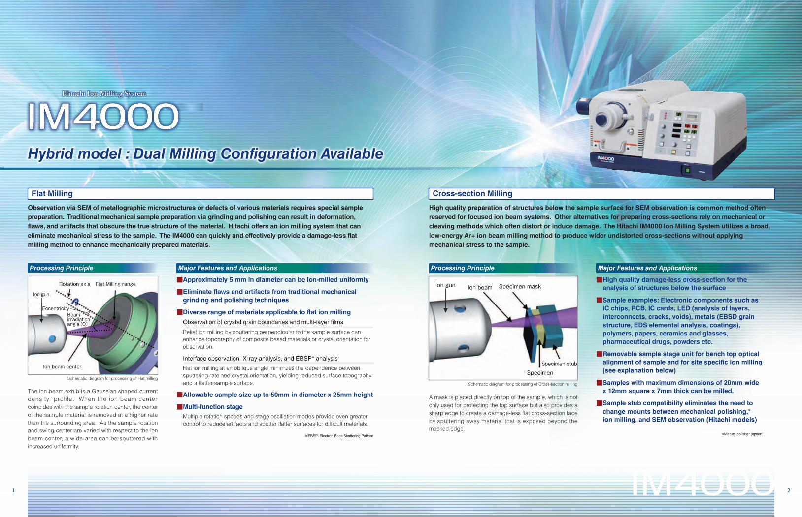
Flat Milling
Observation via SEM of metallographic microstructures or defects of various materials requires special sample
preparation. Traditional mechanical sample preparation via grinding and polishing can result in deformation,
flaws, and artifacts that obscure the true structure of the material. Hitachi offers an ion milling system that can
eliminate mechanical stress to the sample. The IM4000 can quickly and effectively provide a damage-less flat
milling method to enhance mechanically prepared materials.
■Approximately 5 mm in diameter can be ion-milled uniformly
■Eliminate flaws and artifacts from traditional mechanical
grinding and polishing techniques
■Diverse range of materials applicable to flat ion milling Observation of crystal grain boundaries and multi-layer films
Relief ion milling by sputtering perpendicular to the sample surface can
enhance topography of composite based materials or crystal orientation for
observation.
Interface observation, X-ray analysis, and EBSP* analysis
Flat ion milling at an oblique angle minimizes the dependence between
sputtering rate and crystal orientation, yielding reduced surface topography
and a flatter sample surface.
■Allowable sample size up to 50mm in diameter x 25mm height
■Multi-function stage
Multiple rotation speeds and stage oscillation modes provide even greater
control to reduce artifacts and sputter flatter surfaces for difficult materials.
*EBSP:Electron Back Scattering Pattern
Cross-section Milling
High quality preparation of structures below the sample surface for SEM observation is common method often
reserved for focused ion beam systems. Other alternatives for preparing cross-sections rely on mechanical or
cleaving methods which often distort or induce damage. The Hitachi IM4000 Ion Milling System utilizes a broad,
low-energy Ar+ ion beam milling method to produce wider undistorted cross-sections without applying
mechanical stress to the sample.
■High quality damage-less cross-section for the
analysis of structures below the surface
■Sample examples: Electronic components such as
IC chips, PCB, IC cards, LED (analysis of layers,
interconnects, cracks, voids), metals (EBSD grain
structure, EDS elemental analysis, coatings),
polymers, papers, ceramics and glasses,
pharmaceutical drugs, powders etc.
■Removable sample stage unit for bench top optical
alignment of sample and for site specific ion milling
(see explanation below)
■Samples with maximum dimensions of 20mm wide
x 12mm square x 7mm thick can be milled.
■Sample stub compatibility eliminates the need to
change mounts between mechanical polishing,*
ion milling, and SEM observation (Hitachi models)
*Maruto polisher (option)
The ion beam exhibits a Gaussian shaped current
densi ty profile. When the ion beam center
coincides with the sample rotation center, the center
of the sample material is removed at a higher rate
than the surrounding area. As the sample rotation
and swing center are varied with respect to the ion
beam center, a wide-area can be sputtered with
increased uniformity.
Schematic diagram for processing of Flat milling
A mask is placed directly on top of the sample, which is not
only used for protecting the top surface but also provides a
sharp edge to create a damage-less flat cross-section face
by sputtering away material that is exposed beyond the
masked edge.
Schematic diagram for processing of Cross-section milling
Processing Principle Major Features and Applications Processing Principle Major Features and Applications
Ion gun
Eccentricity
Rotation axis Flat Milling range
Ion beam center
Beamirradiation angle(Θ)
Ion beam Specimen mask
Specimen stubSpecimen
Ion gun
3 4
Hitachi Ion Milling System
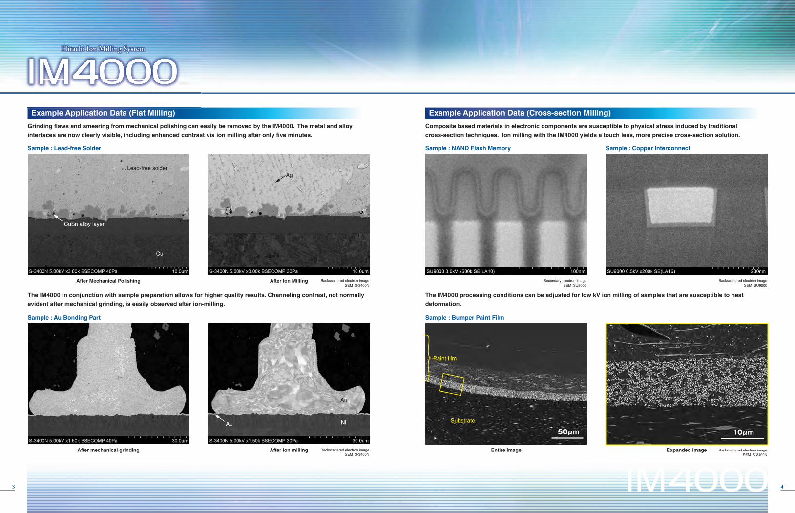
Example Application Data (Flat Milling)
Grinding flaws and smearing from mechanical polishing can easily be removed by the IM4000. The metal and alloy
interfaces are now clearly visible, including enhanced contrast via ion milling after only five minutes.
The IM4000 in conjunction with sample preparation allows for higher quality results. Channeling contrast, not normally
evident after mechanical grinding, is easily observed after ion-milling.
Example Application Data (Cross-section Milling)
Composite based materials in electronic components are susceptible to physical stress induced by traditional
cross-section techniques. Ion milling with the IM4000 yields a touch less, more precise cross-section solution.
Backscattered electron image
SEM:S-3400N
Sample : Lead-free Solder
After Mechanical Polishing After Ion Milling
Backscattered electron image
SEM:S-3400N
Sample : Au Bonding Part
After mechanical grinding After ion milling
The IM4000 processing conditions can be adjusted for low kV ion milling of samples that are susceptible to heat
deformation.
Secondary electron image
SEM:SU9000
Backscattered electron image
SEM:SU9000
Sample : NAND Flash Memory Sample : Copper Interconnect
Sample : Bumper Paint Film
Entire image
50μm
Backscattered electron image
SEM:S-3400N
10μm
Expanded image
CuSn alloy layer
Ag
Cu
Lead-free solder
Au
Au
Paint film
SubstrateNi
5 6
Hitachi Ion Milling System
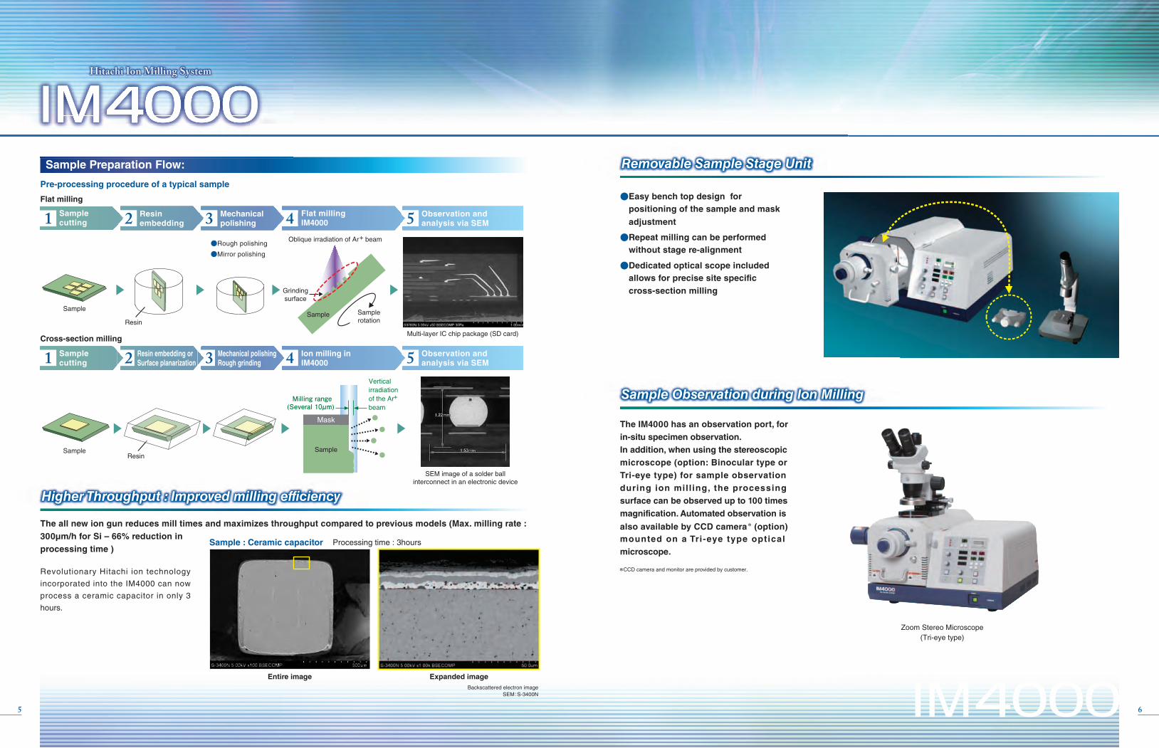
Sample Preparation Flow:
Backscattered electron image
SEM:S-3400N
Expanded image
Higher Throughput : Improved milling efficiency
5 Observation and analysis via SEM4 Flat milling
IM40003 Mechanical polishing2 Resin
embedding1 Sample cutting
Flat milling
5 Observation and analysis via SEM4 Ion milling in
IM40003 Mechanical polishingRough grinding2 Resin embedding or
Surface planarization1 Sample cutting
Cross-section milling
●Rough polishing
●Mirror polishing
Entire image
Revolutionary Hitachi ion technology
incorporated into the IM4000 can now
process a ceramic capacitor in only 3
hours.
Removable Sample Stage Unit
●Easy bench top design for
positioning of the sample and mask
adjustment ●Repeat milling can be performed
without stage re-alignment
●Dedicated optical scope included
allows for precise site specific
cross-section milling
Sample Observation during Ion Milling
The IM4000 has an observation port, for
in-situ specimen observation.
In addition, when using the stereoscopic
microscope (option: Binocular type or
Tri-eye type) for sample observation
during ion mill ing, the processing
surface can be observed up to 100 times
magnification. Automated observation is
also available by CCD camera* (option)
mounted on a Tri-eye type optical
microscope.
The all new ion gun reduces mill times and maximizes throughput compared to previous models (Max. milling rate :
300μm/h for Si – 66% reduction in
processing time )Sample : Ceramic capacitor Processing time : 3hours
Zoom Stereo Microscope
(Tri-eye type)
Sample
Sample
ResinSample
Grindingsurface
Samplerotation
Oblique irradiation of Ar+ beam
Resin
Multi-layer IC chip package (SD card)
Mask
Sample
Milling range (Several 10μm)
SEM image of a solder ballinterconnect in an electronic device
Pre-processing procedure of a typical sample
Vertical
irradiation
of the Ar+
beam
*CCD camera and monitor are provided by customer.
Printed in Japan (H) HTD-E197P 2012.7
Specifications in this catalog are subject to change with or without notice, as Hitachi High-Technologies Corporation continues to develop the latest technologies and products for our customers.
/global/em/
Copyright (C) Hitachi High-Technologies Corporation 2012 All rights reserved.
For technical consultation, please contact:[email protected]
Notice: Follow the instruction manual for proper operation.
System Specifications
Item
Source
Accelerating voltage range
Maximum milling rate *1*2
(Material : Si)
Maximum sample size
Sample moving range
Rotation speed
Swing angle
Tilt
Gas flow rate control system
Evacuation system
Dimension
Weight
Optional Accessories
Zoom stereo microscope unit
Description
Flat Milling Cross-section Milling
Ar (argon) gas
0 to 6kV
Approx. 20μm/h*3 (spot) Approx. 300μm/h*1*2
Approx. 2μm/h*4 (flat)
50(dia.)×25(H)mm 20(W)×12(D)×7(H)mm
X 0 to +5mm X±7mm, Y 0 to +3mm
1r/min, 25r/min −
±60° ±90° ±15° ±30° ±40°
0~90° −
Mass flow controller
Turbo-molecular pump (33L/s) + Rotary Pump(135L/min at 50Hz,162L/min at 60Hz)616(W)×705(D)×312(H)mm
Main unit 48kg + Rotary pump 28kg
Optical microscope for viewing the specimen during milling
Options
Binocular type, Tri-eye type (for CCD)
*1: This rate is the maximum depth obtained when Si is protruded from a mask edge for processing by 100μm.
*2: This rate is the average value obtained when Si is processed for two hours.
*3: Illuminating angle : 60° Eccentric value : 4mm
*4: Illuminating angle : 0° Eccentric value : 0mm
*5: IM4000 is equipped with a power cord with 3-Pin plug.
*6: This piping connects Ar gas supply facilities (Ar gas cylinder) and equipment.
Prepare together with a pressure governor for supply facilities (Ar gas cylinder).
*7: Adequate ventilation and air quality measurements are required.
Installation Requirements
Item
Room Temperature
Humidity
Power supply*5
Grounding
Description
15 to 30°C
45 to 85% without moisture condensation
AC100V (±10%), 50/60Hz, 1.25kVA
100Ω or less
Facilities provided by customer
Item
Ar gas
Ar gas pressure
Ar gas piping*6
Oxygen content meter*7
Recommended table
Description
99.99% purity
0.03 to 0.05MPa
1/8-inch SUS piping (1/8 Swagelok-compatible),
Pressure regulator
19% oxygen concentration
1000(W)×800(D)×700(H)mm or more,
Min. weight tolerance : 70kg (Minimum strength when
installing only IM4000 on the desk)
System layout
140
77
200
705
140
1,000
490616
Table (700 high)
Unit : mm
• Power cord 3 m
• Ar gas piping 2 m or less
Optical microscope
Rotary pumpArgon gas cylinder
(Provided by
customer)
800
Related Documents