76 · History and Future Development of Heat Spreader Products FEATURED TOPIC 1. Introduction In the 1960s, when silicon semiconductor chips improved in power and circuit density, heat resulting from these improvements and mismatches in the coeffi- cient of thermal expansion caused cracks to develop in the bonding layer (solder or brazing filler metal) between the chip and base plate. In some extreme cases, fractures developed in chips. As a solution to this problem, semiconductor manufacturers sought materials other than copper (Cu) or aluminum (Al) conventionally used to construct base plates. Later, the base plate became commonly known as the “heat spreader.” Properties required for heat spreader include: ( 1) higher thermal conductivity (TC), (2) optimum coefficient of thermal expansion (CTE), and (3) good bondability between the semiconductor chip and solder (or brazing filler metal). As materials that meet heat spreader requirements, tungsten (W)- and molybdenum (Mo)-based products, which were produced using the basic technologies of Tokyo Tungsten and Sumitomo Electric, became the focus of attention (Fig. 1 and Table 1). 2. Use of Mo as a Heat Spreader Material In the early 1960s, large electronics manufacturers started a development project to use large silicon (Si) semiconductors (50 to 60 mm in dia.) as an alternative to mercury-arc rectifiers for high-power control. To avoid cracks in Si chips, the project selected Mo as the base plate material because of the thermal expansion History and Future Development of Heat Spreader Products Hiroshi KATSUTANI*, Shinichi YAMAGATA and Izumi NAKAMURA ---------------------------------------------------------------------------------------------------------------------------------------------------------------------------------------------------------------------------------------------------------- Heat spreaders, the heat radiation base plates of semiconductor devices, are designed for efficient heat dissipation and heat stress reduction. The number of heat spreaders made from tungsten- and molybdenum-based materials using a technology developed by Tokyo Tungsten Co., Ltd.* and Sumitomo Electric Industries, Ltd. has been increasing. This paper introduces the history of heat spreaders, including the changes in the microprocessors of personal computers, insulated gate bipolar transistor modules inside hybrid vehicles, and high frequency devices for cellular phone base stations. The development of new materials, such as diamond and ceramics, is also covered. * Tokyo Tungsten Co., Ltd.: Merged with Osaka Diamond Industrial Co., Ltd to form A.L.M.T. Corp., a Sumitomo Electric Group company ---------------------------------------------------------------------------------------------------------------------------------------------------------------------------------------------------------------------------------------------------------- Keywords: semiconductor heat spreader, thermal conductivity, coefficient of thermal expansion, solder joint, composite material 0 5 10 15 20 25 100 140 160 180 200 220 240 260 280 300 400 500 2000 120 Si GaAs InP GaN Al2O3 high C.T.E. Glass Ceramics FR-4 Cu W Mo Cu-Mo AlN Cu-W Mg-SiC Diamond Al Thermal properties of Heatspreader Materials Thermal Conductivity(W/m・K) Coefficient of Thermal Expansion(ppm/K) Sintered Al-SiC SiC Fig. 1. Properties of heat spreader materials Table 1. Properties of heat spreader materials 4.5 167 19.3 5.1 159 10.2 Cu-W W-10 89W-11Cu 6.5 180 17 PCM35 65Mo-35Cu 7.7 210 9.7 CPC141 Cu/PCM/Cu 8.5 220 9.5 Ceramics AlN 4.5 200 3.26 Al-Si A-40 60Al-40Si 13 126 2.53 Al-SiC β8 70SiC-30Al 8 140 2.6 Mg-SiC MgSiC 18Mg-SiC 7.5 230 2.7 Cu-Dia DC60 Dia-Cu 6 550 5 2.3 2000 3.52 2.3 1000 3.52 3 151 2.3 5.9 46 5.32 4.5 70 4.79 5.6 130 6.15 3.1 490 3.2 6.7 17 3.6 17 393 8.93 23 238 2.7 5.3 17 8.36 16 0.2 - 25 0.2 - InP GaN SiC Ceramic-Metal Composites Polyimide Semiconductors Organic Materials Metals Diamonds GaAs CTE [ppm/K] at 25°C Sumicrystal™ CVD diamond SALN-20 Material Trade name Composition W Mo Cu-Mo Class Metals Plastic FR-4 TC [W/(m・K)] at 25°C Specific Gravity Heat spreaders Composite Metals Reference Data Ceramics Al2O3 Cu Al Kovar Si

Welcome message from author
This document is posted to help you gain knowledge. Please leave a comment to let me know what you think about it! Share it to your friends and learn new things together.
Transcript

76 · History and Future Development of Heat Spreader Products
FEATURED TOPIC
1. Introduction
In the 1960s, when silicon semiconductor chips improved in power and circuit density, heat resulting from these improvements and mismatches in the coeffi-cient of thermal expansion caused cracks to develop in the bonding layer (solder or brazing filler metal) between the chip and base plate. In some extreme cases, fractures developed in chips.
As a solution to this problem, semiconductor manufacturers sought materials other than copper (Cu) or aluminum (Al) conventionally used to construct base plates. Later, the base plate became commonly known as the “heat spreader.” Properties required for heat
spreader include: ( 1 ) higher thermal conductivity (TC), (2) optimum coefficient of thermal expansion (CTE), and (3) good bondability between the semiconductor chip and solder (or brazing filler metal). As materials that meet heat spreader requirements, tungsten (W)- and molybdenum (Mo)-based products, which were produced using the basic technologies of Tokyo Tungsten and Sumitomo Electric, became the focus of attention (Fig. 1 and Table 1).
2. Use of Mo as a Heat Spreader Material
In the early 1960s, large electronics manufacturers started a development project to use large silicon (Si) semiconductors (50 to 60 mm in dia.) as an alternative to mercury-arc rectifiers for high-power control. To avoid cracks in Si chips, the project selected Mo as the base plate material because of the thermal expansion
History and Future Development of Heat Spreader Products
Hiroshi KATSUTANI*, Shinichi YAMAGATA and Izumi NAKAMURA
----------------------------------------------------------------------------------------------------------------------------------------------------------------------------------------------------------------------------------------------------------Heat spreaders, the heat radiation base plates of semiconductor devices, are designed for efficient heat dissipation and heat stress reduction. The number of heat spreaders made from tungsten- and molybdenum-based materials using a technology developed by Tokyo Tungsten Co., Ltd.* and Sumitomo Electric Industries, Ltd. has been increasing. This paper introduces the history of heat spreaders, including the changes in the microprocessors of personal computers, insulated gate bipolar transistor modules inside hybrid vehicles, and high frequency devices for cellular phone base stations. The development of new materials, such as diamond and ceramics, is also covered.* Tokyo Tungsten Co., Ltd.: Merged with Osaka Diamond Industrial Co., Ltd to form A.L.M.T. Corp., a Sumitomo Electric Group company
----------------------------------------------------------------------------------------------------------------------------------------------------------------------------------------------------------------------------------------------------------Keywords: semiconductor heat spreader, thermal conductivity, coefficient of thermal expansion, solder joint, composite material
0 5 10 15 20 25
100
140
160
180
200
220
240
260
280
300
400
500
2000
120Si
GaAs
InPGaN
Al2O3
high C.T.E. Glass Ceramics
FR-4
Cu
W
Mo
Cu-Mo
AlN Cu-W
Mg-SiC
Diamond
Al
Thermal properties of Heatspreader Materials
Ther
mal
Con
duct
ivity(
W/m
・K)
Coefficient of Thermal Expansion(ppm/K)
Sintered Al-SiC
SiC
Fig. 1. Properties of heat spreader materials
Table 1. Properties of heat spreader materials
4.5 167 19.35.1 159 10.2
Cu-W W-10 89W-11Cu 6.5 180 17PCM35 65Mo-35Cu 7.7 210 9.7CPC141 Cu/PCM/Cu 8.5 220 9.5
Ceramics AlN 4.5 200 3.26Al-Si A-40 60Al-40Si 13 126 2.53
Al-SiC β8 70SiC-30Al 8 140 2.6Mg-SiC MgSiC 18Mg-SiC 7.5 230 2.7Cu-Dia DC60 Dia-Cu 6 550 5
2.3 2000 3.522.3 1000 3.52
3 151 2.35.9 46 5.324.5 70 4.795.6 130 6.153.1 490 3.26.7 17 3.617 393 8.9323 238 2.75.3 17 8.3616 0.2 -25 0.2 -
InPGaNSiC
Ceramic-MetalComposites
Polyimide
Semiconductors
Organic Materials
Metals
Diamonds
GaAs
CTE[ppm/K] at 25°C
Sumicrystal™CVD diamond
SALN-20
Material Trade name Composition
WMo
Cu-Mo
Class
Metals
Plastic FR-4
TC[W/(m・K)]
at 25°C
SpecificGravity
Hea
t spr
eade
rs
Composite Metals
Ref
eren
ce D
ata
Ceramics Al2O3CuAl
Kovar
Si

SEI TECHNICAL REVIEW · NUMBER 82 · APRIL 2016 · 77
coefficient similar to that of Si. After many reliability tests, Mo base plates manufactured by Tokyo Tungsten were chosen for the first time for power converters (thyristors) on the Shinkansen, a high-speed railway line in Japan, which opened in 1964. Subsequently, in the 1970s, when a long-term reliability problem emerged with in-vehicle semiconductors, a three-layer structure comprising a Si semiconductor chip, a thin Mo plate, and a copper (Cu) heat spreader was developed and used to lower the thermal stresses and solve the problem. For more than 40 years Tokyo Tungsten, now A.L.M.T. Tech Inc., has shipped around 20 different types of heat spreaders in high volume with plate sizes ranging from 3 x 3 mm to 16 x 16 mm square and 0.5 to 1.5 mm thick. These products were/are mostly plated [solder plated in the early days, followed later by nickel (Ni) plating] to ensure favorable wettability for use with solder. Tokyo Tungsten developed its original tech-nology to achieve stable Ni plating on Mo. Moreover, Tokyo Tungsten developed a pre soldering technology to pre bond solder onto thin Mo plates, thereby helping their customers improve productivity.
3. Cu-W as a Heat Spreader Material for Ceramic Packages
Tokyo Tungsten was shipping W powders to ceramic package manufacturers for metallization and setter plates made of Mo for firing ceramics. In the spring of 1982, one of Tokyo Tungsten’s major customers informed Tokyo Tungsten of the need for heat spreaders designed to improve the heat dissipa-tion performance of integrated circuit (IC) ceramic packages (pin grid arrays). Tokyo Tungsten notified Sumitomo Electric that their customer had constructed a prototype package using a US-made copper-tungsten (Cu-W) composite and that the prototype package had poor yield due to the warpage caused by the CTE mismatch between materials. Despite the excellent heat dissipation performance of the composite, the poor yield did not justify the use of the composite for prod-ucts. Choosing Cu-W as the first candidate material for the IC package heat spreader, Sumitomo Electric tried to control and regulate its CTE to reduce variation and to better match it with the CTE of alumina (Al2O3), the primary material used in IC packages. Tokyo Tungsten had more than 30 years of experience in producing Cu-W as a material for electrical contacts through a powder metallurgical process (sintering or infiltration). However, electrical contacts were mostly large products (20 x 20 mm to 50 x 50 mm square and 2 to 5.0 mm thick), and for most part did not take CTE variation fully into consideration. Accordingly, Tokyo Tungsten returned to the drawing board and began working on the development of the desired Cu-W by redesigning almost the entire process. About one year later, a new material (10% Cu and 90% W) produced by infiltration was launched under the trade name of CMSH W-10 (Photo 1).
In July 1982, Sumitomo Electric applied for a patent on the material (sintered solid of Cu and W or Cu and Mo for use as a semiconductor substrate) and applica-tion of the same. (Later, the patent numbered 2135368 was granted.) Subsequently, soon after Sumitomo Electric’s patent application was submitted, it was learned that their partner in the development, and a customer whom Sumitomo Electric was trying to sell product to had applied for patents for an alumina package incorporating Cu-W. As one of the patent applications was submitted earlier than Sumitomo Electric’s, Sumitomo Electric quickly purchased the patent in question and enjoyed the upper hand in terms of patents. In the spring of 1983, Sumitomo Electric won the first volume order for the material and sales grew steadily. Despite growth in sales, customers requested a substantially lower price level than that of electrical contact materials. To meet their request, Sumitomo Electric made active cost reduction efforts by intro-ducing inexpensive equipment to manufacture the material in-house and by promoting automation. Additionally, it became necessary for heat spreaders to meet strict dimensional tolerances and surface rough-ness requirements, and so Sumitomo Electric intro-duced honing and lapping machines to improve the finishing process. Furthermore, in order to expand sales, Sumitomo Electric began marketing efforts targeting package manufacturers both domestically and abroad. Thereafter, sales grew steadily from IC package applica-tions to use as device heatsinks in large computers. In parallel, Sumitomo Electric developed Cu-W plating techniques as in-house processes, automated work piece loading and ejection onto and from numerically controlled (NC) milling machines, and gradually improved in cost competitiveness.
In August 1991, Sumitomo Electric and Tokyo Tungsten invested 50% each to found a manufacturing company specializing in heatsinks named Advanced Materials Incorporated (AMI) in Yamagata, Japan thereby completing two heat spreader-manufacturing sites in Japan.
In 1993, W-10 was chosen as the heat spreader for
Photo 1. Cu-W heat spreaders for various applications

78 · History and Future Development of Heat Spreader Products
central processing units (CPUs) in personal computers then rapidly coming into widespread use. To meet the demand, Sumitomo Electric dramatically boosted production of the W-10 (Fig. 2).
In 1995, the Great Hanshin-Awaji Earthquake occurred, which greatly affected the Itami Works, the main plant manufacturing Cu-W, and stopped its production. AMI in Yamagata was not affected by the earthquake and began producing additional heat spreaders to make up for the stoppage at the Itami Works. In the process, AMI radically boosted their production in order to overcome the unparalleled dire situation. This was a perfect example of the value of having two domestic manufacturing sites under the business continuity plan (BCP). The demand for the W-10 grew steadily for four years and achieved record sales in 1997. However, due to advances in mounting techniques, described later, and a shift in package mate-rial from ceramic to plastic demand for W-10 as a heat spreader for CPUs concluded by 2000. Nonetheless, Cu-W has remained in demand and in production, as a key material of heat spreaders for use in cellular base stations and for optical communications.
4. Development of Low-Cost Cu-Mo Heat Spreaders and Three Layer- Structured CPC
While the earlier heat spreader material of Cu-W was thriving in the 1990s, Tokyo Tungsten succeeded in developing a copper-molybdenum (Cu-Mo) composite material in 1997. This material could be formed into large ingots through an infiltration process and was also compatible with low-cost engineering methods such as rolling and stamping unlike Cu-W, which required finishing by machining. Thereafter, because Cu-Mo is higher in TC and lighter in weight than Cu-W, Cu-Mo increasingly replaced Cu-W. In 1998, using a similar technique to the Cu-Mo-Cu (CMC) cladding developed in the early 1990s, Tokyo Tungsten successfully devel-oped a material with a Cu-Mo (PCM) core clad with Cu. This three-layer structure was called CPC [Cu-PCM-Cu]. To this date, Cu-Mo and CPC have remained key mate-rials for heat spreaders.
The event that served as a springboard for the
development of the Cu-Mo material was the develop-ment of hybrid electric vehicles (HEVs). In the heart of HEVs, an inverter is used to convert the direct current (DC) of the drive batteries into an alternating current (AC) to power the motor. In doing this, the inverter produces a large amount of heat. In order to dissipate this heat, HEVs employed a structure in which three to four large heat spreaders (approx. 180 x 80 mm rect-angle 3 mm in thickness) were inserted between a water-cooled radiator and an insulated gate bipolar transistor (IGBT) chip (Fig. 3). At first, the HEV manu-facturer used US-made Al-SiC for the heat spreaders, however, due to a quality issue related to the solder wettability of Al-SiC, followed by problems with the Al-SiC manufacturer, Tokyo Tungsten’s Cu-Mo was quickly selected as an alternative to Al-SiC. This was a result of the company’s thorough marketing and devel-opment efforts.
Subsequently, the following year’s vehicle model, launched in 2003, selected the new CPC material for use as the heat spreader. Additionally, by way of an electrical equipment manufacturer, CPC heat spreaders were adopted for use in converters provided for DC-AC conversion between motors and batteries as well as between generators and batteries. HEVs’ popularity continued to grow, and in addition to the boost in HEV production, the number of HEV models also rapidly increased, with the demand for heatsinks growing at a far faster pace than initially imagined. Despite the opti-mization of the production floor layout of the existing plant in AMI, demand quickly outpaced capacity, in December of 2005, a new plant was built specializing in the manufacture of heat spreaders for HEVs. The new plant achieved productivity improvement, minimizing loss from transfer by integrating the production of Cu-Mo alloys from alloying to machining, plating and inspection.
Meanwhile, the price of the raw material, molyb-denum powder, increased dramatically. Using the price of molybdenum oxide as a reference rate, the price increased more than six-fold from $3-$5 per pound to over $30. Due to traditionally small price fluctuations, before this dramatic price increase, A.L.M.T. Tech Inc. did not use a raw material-based index-linking system for
Cu-W
Ceramic package
Si chip
Pin
Fig. 2. Early structural schematic of personal computer CPU with Cu-W heat spreader
Cu-Mo Al substrate
SolderAlN Al (DBA substrate)
Screw
Cooling water
Si chip
Fig. 3. Structural schematic of HEV inverter device incorporating Cu-Mo heat spreader
SEI TECHNICAL REVIEW · NUMBER 82 · APRIL 2016 · 79
the quoting of Mo and Cu-Mo products. Accordingly, while the fixed price system under which the initial quotations for Mo and Cu-Mo based products remained, business was placed into a very difficult and costly situ-ation. The sales staff made great efforts to explain the situation to customers and persuade them to agree to a Mo-based index-linking system for Mo products.
Incidentally, the plants worked on reducing mate-rial loss and on increasing yield, eventually leading to the mastery of various improvement techniques and substantial improvements in productivity. In April 2005, A.L.M.T. Tech Inc. commenced its Total Plant Management (TPM) campaign, which took root and has been continuing in AMI. In 2008, almost all HEVs distrib-uted in Japan started to use heat spreaders manufac-tured by A.L.M.T. Tech Inc. Subsequently, however, inverters and converters evolved in structure so as not to need heat spreaders. In 2014, the use of Cu-Mo heat-sinks in HEVs has almost disappeared.
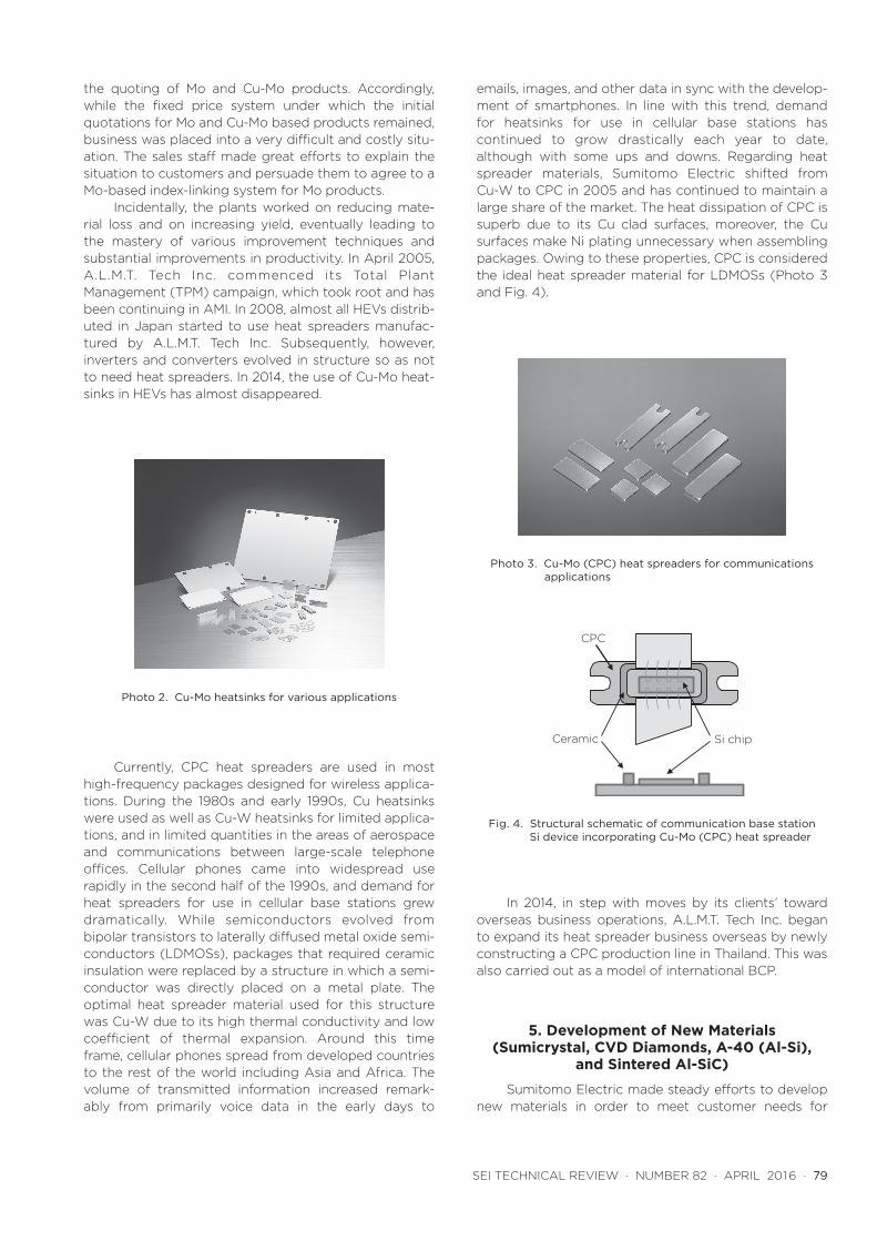
Currently, CPC heat spreaders are used in most high-frequency packages designed for wireless applica-tions. During the 1980s and early 1990s, Cu heatsinks were used as well as Cu-W heatsinks for limited applica-tions, and in limited quantities in the areas of aerospace and communications between large-scale telephone offices. Cellular phones came into widespread use rapidly in the second half of the 1990s, and demand for heat spreaders for use in cellular base stations grew dramatically. While semiconductors evolved from bipolar transistors to laterally diffused metal oxide semi-conductors (LDMOSs), packages that required ceramic insulation were replaced by a structure in which a semi-conductor was directly placed on a metal plate. The optimal heat spreader material used for this structure was Cu-W due to its high thermal conductivity and low coefficient of thermal expansion. Around this time frame, cellular phones spread from developed countries to the rest of the world including Asia and Africa. The volume of transmitted information increased remark-ably from primarily voice data in the early days to
emails, images, and other data in sync with the develop-ment of smartphones. In line with this trend, demand for heatsinks for use in cellular base stations has continued to grow drastically each year to date, although with some ups and downs. Regarding heat spreader materials, Sumitomo Electric shifted from Cu-W to CPC in 2005 and has continued to maintain a large share of the market. The heat dissipation of CPC is superb due to its Cu clad surfaces, moreover, the Cu surfaces make Ni plating unnecessary when assembling packages. Owing to these properties, CPC is considered the ideal heat spreader material for LDMOSs (Photo 3 and Fig. 4).
In 2014, in step with moves by its clients’ toward overseas business operations, A.L.M.T. Tech Inc. began to expand its heat spreader business overseas by newly constructing a CPC production line in Thailand. This was also carried out as a model of international BCP.
5. Development of New Materials (Sumicrystal, CVD Diamonds, A-40 (Al-Si),
and Sintered Al-SiC)
Sumitomo Electric made steady efforts to develop new materials in order to meet customer needs for
Photo 2. Cu-Mo heatsinks for various applications
CPC
Ceramic Si chip
Photo 3. Cu-Mo (CPC) heat spreaders for communications applications
Fig. 4. Structural schematic of communication base station Si device incorporating Cu-Mo (CPC) heat spreader

80 · History and Future Development of Heat Spreader Products
higher thermal conductivity and further weight reduc-tion, due to limitations in this regard of W- and Mo-based materials. In the period from 1982 to the early 1990s, Sumitomo Electric succeeded in developing Sumicrystal, CVD diamonds, and the A-40 (a new mate-rial produced through a powder metallurgy process by adding Si to Al in a ratio of 40:60, the development of which was completed in 1987 by the Itami Research Laboratory). Active marketing contributed to Sumicrystal and CVD diamonds being selected in the laser sector that requires high TC, and to the A-40 being adopted in the aerospace sector that requires light weight.
In 1994, new demand for heat spreaders arose in relation to the mounting of personal computer CPUs. More specifically, the design was a radical methodolog-ical change from the conventional way of having the package provide both the electrical wiring and heat dissipation to a new way of using the package only for the purpose of electrical wiring and placing a concave lid atop the chip for heat dissipation. Consequently, the lid material needed to be highly thermally conductive and lightweight.
To meet this demand, Sumitomo Electric developed sintered Al-SiC, using its specialized powder metallurgy technology. This material was produced without machining by blending powders of lightweight and highly thermally conductive aluminum (Al) and silicon carbide (SiC) at a suitable ratio for the required level of thermal expansion, loading the mixture in a mold to form a lid, and sintering the formed lid. Although Al-SiC mate-rials produced by infiltrating molten Al into a porous SiC body under pressure were commercially available from other manufacturers, sintered Al-SiC was a milestone material because it did not require large pressurization equipment to manufacture nor machining to shape it after the material was produced. Sumitomo Electric obtained a patent on sintered Al-SiC and encouraged the selection of this material by its potential customers (Photo 4).
Contrary to expectations, the packaging design for personal computer CPUs shifted from ceramic to plastic
with plastic packages enabling the use of lids made from aluminum alloys or copper. This shift caused a downslide in the demand for sintered Al-SiC as Al-SiC failed to maintain a foothold in the personal computer CPU market. Around the turn of the century, however, demand for computer servers began to increase and sintered Al-SiC was selected in a wide range of server applications. Large computer and semiconductor manu-facturers in Japan and abroad successively selected sintered Al-SiC as their CPU heat spreader material of choice, allowing the material to enjoy a period of domi-nance (Fig. 5). Moreover, having developed Si-SiC as a derivative material, Sumitomo Electric gained a long-sought business opportunity with the world’s largest computer manufacturers. Incidentally, and to the extreme delight of those involved with the development and marketing of Al-SiC material, the “K” supercom-puter, the world’s fastest supercomputer in 2012, also incorporated sintered Al-SiC heat spreaders into its design.
Due to price competitiveness, current trends show a decline in the usage of sintered Al-SiC in servers while Cu has enjoyed a rebound in demand since around 2004. However, sintered Al-SiC has been continuously in demand for automotive engine control unit (ECU) appli-cations. These products are being produced at the Toyama Works of A.L.M.T. Corp., established in 2004 as a spin-off from Itami Works. The heat spreader division in Toyama serves as the central location for heat spreader material development and is currently preparing for the mass production of a new product called Mg-SiC, a successor to sintered Al-SiC. Sumitomo Electric has also developed and improved other materials such as Cu-Dia, a successor material to Sumicrystal, and CVD diamond, and already has plans to launch a new diamond based material as a successor to Cu-Dia.
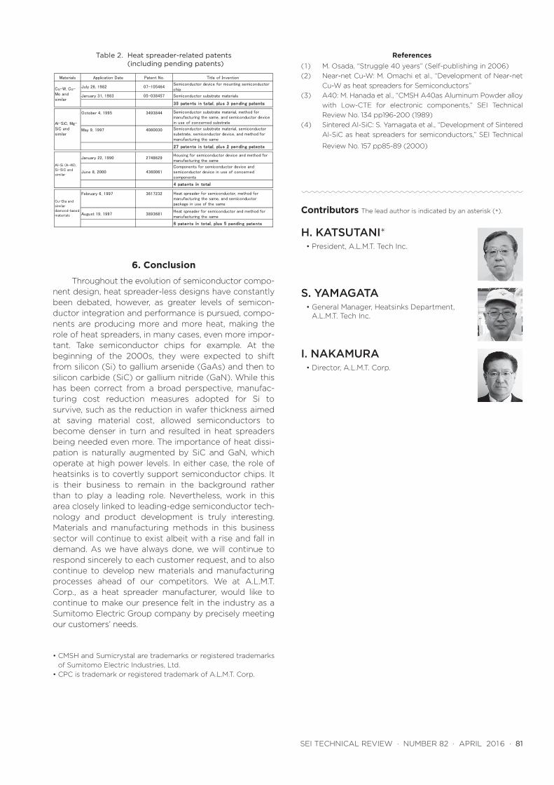
Table 2 shows Sumitomo Electric’s heat spreader-related patents granted to date (including pending patents).
Photo 4. Al-SiC heat spreaders for various applications
Sintered Al-SiC
Ceramic package(BGA)
Si chip Solder ball
Fig. 5. Structural schematic of sintered Al-SiC used in PC server or large computer applications
SEI TECHNICAL REVIEW · NUMBER 82 · APRIL 2016 · 81
6. Conclusion
Throughout the evolution of semiconductor compo-nent design, heat spreader-less designs have constantly been debated, however, as greater levels of semicon-ductor integration and performance is pursued, compo-nents are producing more and more heat, making the role of heat spreaders, in many cases, even more impor-tant. Take semiconductor chips for example. At the beginning of the 2000s, they were expected to shift from silicon (Si) to gallium arsenide (GaAs) and then to silicon carbide (SiC) or gallium nitride (GaN). While this has been correct from a broad perspective, manufac-turing cost reduction measures adopted for Si to survive, such as the reduction in wafer thickness aimed at saving material cost, allowed semiconductors to become denser in turn and resulted in heat spreaders being needed even more. The importance of heat dissi-pation is naturally augmented by SiC and GaN, which operate at high power levels. In either case, the role of heatsinks is to covertly support semiconductor chips. It is their business to remain in the background rather than to play a leading role. Nevertheless, work in this area closely linked to leading-edge semiconductor tech-nology and product development is truly interesting. Materials and manufacturing methods in this business sector will continue to exist albeit with a rise and fall in demand. As we have always done, we will continue to respond sincerely to each customer request, and to also continue to develop new materials and manufacturing processes ahead of our competitors. We at A.L.M.T. Corp., as a heat spreader manufacturer, would like to continue to make our presence felt in the industry as a Sumitomo Electric Group company by precisely meeting our customers’ needs.
• CMSH and Sumicrystal are trademarks or registered trademarks of Sumitomo Electric Industries, Ltd.
• CPC is trademark or registered trademark of A.L.M.T. Corp.
References(1) M. Osada, “Struggle 40 years” (Self-publishing in 2006)(2) Near-net Cu-W: M. Omachi et al., “Development of Near-net
Cu-W as heat spreaders for Semiconductors”(3) A40: M. Hanada et al., “CMSH A40as Aluminum Powder alloy
with Low-CTE for electronic components,” SEI Technical Review No. 134 pp196-200 (1989)
(4) Sintered Al-SiC: S. Yamagata et al., “Development of Sintered Al-SiC as heat spreaders for semiconductors,” SEI Technical
Review No. 157 pp85-89 (2000)
Contributors The lead author is indicated by an asterisk (*).
H. KATSUTANI*• President, A.L.M.T. Tech Inc.
S. YAMAGATA• General Manager, Heatsinks Department,
A.L.M.T. Tech Inc.
I. NAKAMURA• Director, A.L.M.T. Corp.
Table 2. Heat spreader-related patents (including pending patents)
Materials Application Date Patent No. Title of Invention
July 26, 1982 07-105464Semiconductor device for mounting semiconductorchip
January 31, 1983 05-038457 Semiconductor substrate materials
35 patents in total, plus 3 pending patents
October 4, 1995 3493844
May 9, 1997 4080030
27 patents in total, plus 2 pending patents
January 22, 1990 2748629Housing for semiconductor device and method formanufacturing the same
June 8, 2000 4360061Components for semiconductor device andsemiconductor device in use of concernedcomponents
4 patents in total
February 6, 1997 3617232
August 19, 1997 3893681Heat spreader for semiconductor and method formanufacturing the same
6 patents in total, plus 5 pending patents
Semiconductor substrate material, method formanufacturing the same, and semiconductor devicein use of concerned substrate
Semiconductor substrate material, semiconductorsubstrate, semiconductor device, and method formanufacturing the same
Heat spreader for semiconductor, method formanufacturing the same, and semiconductorpackage in use of the same
Al-Si (A-40),Si-SiC andsimilar
Cu-W, Cu-Mo andsimilar
Al-SiC, Mg-SiC andsimilar
Cu-Dia andsimilardiamond-basedmaterials
Related Documents