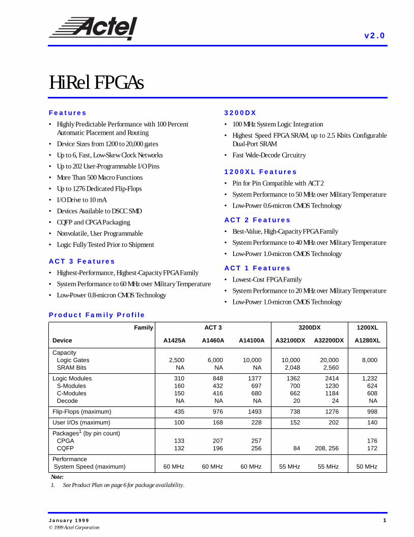
January 1999 1 © 1999 Actel Corporation v2.0 HiRel FPGAs Features • Highly Predictable Performance with 100 Percent Automatic Placement and Routing • Device Sizes from 1200 to 20,000 gates • Up to 6, Fast, Low-Skew Clock Networks • Up to 202 User-Programmable I/O Pins • More Than 500 Macro Functions • Up to 1276 Dedicated Flip-Flops • I/O Drive to 10 mA • Devices Available to DSCC SMD • CQFP and CPGA Packaging • Nonvolatile, User Programmable • Logic Fully Tested Prior to Shipment ACT 3 Features • Highest-Performance, Highest-Capacity FPGA Family • System Performance to 60 MHz over Military Temperature • Low-Power 0.8-micron CMOS Technology 3200DX • 100 MHz System Logic Integration • Highest Speed FPGA SRAM, up to 2.5 Kbits Configurable Dual-Port SRAM • Fast Wide-Decode Circuitry 1200XL Features • Pin for Pin Compatible with ACT 2 • System Performance to 50 MHz over Military Temperature • Low-Power 0.6-micron CMOS Technology ACT 2 Features • Best-Value, High-Capacity FPGA Family • System Performance to 40 MHz over Military Temperature • Low-Power 1.0-micron CMOS Technology ACT 1 Features • Lowest-Cost FPGA Family • System Performance to 20 MHz over Military Temperature • Low-Power 1.0-micron CMOS Technology Product Family Profile Family ACT 3 3200DX 1200XL Device A1425A A1460A A14100A A32100DX A32200DX A1280XL Capacity Logic Gates SRAM Bits 2,500 NA 6,000 NA 10,000 NA 10,000 2,048 20,000 2,560 8,000 Logic Modules S-Modules C-Modules Decode 310 160 150 NA 848 432 416 NA 1377 697 680 NA 1362 700 662 20 2414 1230 1184 24 1,232 624 608 NA Flip-Flops (maximum) 435 976 1493 738 1276 998 User I/Os (maximum) 100 168 228 152 202 140 Packages 1 (by pin count) CPGA CQFP 133 132 207 196 257 256 84 208, 256 176 172 Performance System Speed (maximum) 60 MHz 60 MHz 60 MHz 55 MHz 55 MHz 50 MHz Note: 1. See Product Plan on page 6 for package availability.

Welcome message from author
This document is posted to help you gain knowledge. Please leave a comment to let me know what you think about it! Share it to your friends and learn new things together.
Transcript
v2.0
HiRel FPGAs
Features• Highly Predictable Performance with 100 Percent Automatic Placement and Routing
• Device Sizes from 1200 to 20,000 gates
• Up to 6, Fast, Low-Skew Clock Networks
• Up to 202 User-Programmable I/O Pins
• More Than 500 Macro Functions
• Up to 1276 Dedicated Flip-Flops
• I/O Drive to 10 mA
• Devices Available to DSCC SMD
• CQFP and CPGA Packaging
• Nonvolatile, User Programmable
• Logic Fully Tested Prior to Shipment
ACT 3 Features
• Highest-Performance, Highest-Capacity FPGA Family
• System Performance to 60 MHz over Military Temperature
• Low-Power 0.8-micron CMOS Technology
3200DX
• 100 MHz System Logic Integration
• Highest Speed FPGA SRAM, up to 2.5 Kbits ConfigurableDual-Port SRAM
• Fast Wide-Decode Circuitry
1200XL Features
• Pin for Pin Compatible with ACT 2
• System Performance to 50 MHz over Military Temperature
• Low-Power 0.6-micron CMOS Technology
ACT 2 Features
• Best-Value, High-Capacity FPGA Family
• System Performance to 40 MHz over Military Temperature
• Low-Power 1.0-micron CMOS Technology
ACT 1 Features
• Lowest-Cost FPGA Family
• System Performance to 20 MHz over Military Temperature
• Low-Power 1.0-micron CMOS Technology
Product Family Profile
Family ACT 3 3200DX 1200XL
Device A1425A A1460A A14100A A32100DX A32200DX A1280XL
CapacityLogic GatesSRAM Bits
2,500NA
6,000NA
10,000NA
10,0002,048
20,0002,560
8,000
Logic ModulesS-ModulesC-ModulesDecode
310160150NA
848432416NA
1377697680NA
1362700662
20
241412301184
24
1,232624608NA
Flip-Flops (maximum) 435 976 1493 738 1276 998
User I/Os (maximum) 100 168 228 152 202 140
Packages1 (by pin count)CPGACQFP
133132
207196
257256 84 208, 256
176172
PerformanceSystem Speed (maximum) 60 MHz 60 MHz 60 MHz 55 MHz 55 MHz 50 MHz
Note:1. See Product Plan on page 6 for package availability.
January 1999 1© 1999 Actel Corporation

High-Reliability, Low-Risk Solution
Actel builds the most reliable field programmable gate arrays(FPGAs) in the industry, with overall antifuse reliabilityratings of less than 10 Failures-In-Time (FITs),corresponding to a useful life of more than 40 years. ActelFPGAs have been production proven, with more than fivemillion devices shipped and more than one trillion antifusesmanufactured. Actel devices are fully tested prior toshipment, with an outgoing defect level of only 122 ppm.(Further reliability data is available in the “Actel DeviceReliability Report.”)
100 Percent Tested
Device functionality is fully tested before shipment andduring device programming. Routing tracks, logic modules,and programming, debug, and test circuits are 100 percenttested before shipment. Antifuse integrity also is testedbefore shipment. Programming algorithms are tested when adevice is programmed using Actel’s Activator® 2 or Activator2S programming stations.
Benefits
No Cost Risk—Once you have a Designer/DesignerAdvantage™ System, Actel’s CAE software and programmingpackage, you can produce as many chips as you like for justthe cost of the device itself, with no NRE charges to eat upyour development budget every time you want to try out a newdesign.
No Time Risk—After entering your design, placement androuting is automatic, and programming the device takes onlyabout 5 to 15 minutes for an average design. You save time inthe design entry process by using tools that are familiar toyou. The Designer/Designer Advantage System softwareinterfaces with popular CAE packages such as Cadence,Mentor Graphics, OrCAD, and Viewlogic, running onplatforms such as HP, Sun, and PC. In addition, synthesiscapability is provided with support of synthesis tools fromSynopsys, IST, Exemplar, and DATA I/O.
No Reliability Risk—The PLICE® antifuse is a one-timeprogrammable, nonvolatile connection. Since Actel devicesare permanently programmed, no downloading from EPROMor SRAM storage is required. Inadvertent erasure isimpossible, and there is no need to reload the program afterpower disruptions. Fabrication using a low-power CMOSprocess means cooler junction temperatures. Actel’s non-PLDarchitecture delivers lower dynamic operating current. Ourreliability tests show a very low failure rate of 66 FITs at 90°Cjunction temperature with no degradation in ACperformance. Special stress testing at wafer test eliminatesinfant mortalities prior to packaging.
No Security Risk—Reverse engineering of programmed Acteldevices from optical or electrical data is extremely difficult.Programmed antifuses cannot be identified from aphotograph or by using a SEM. The antifuse map cannot bedeciphered either electrically or by microprobing. Each
Product Family Profile
Family ACT 2 ACT 1
Device A1240A A1280A A1010B A1020B
CapacityLogic GatesSRAM Bits
4,000NA
8,000NA
1,200NA
2,000NA
Logic ModulesS-ModulesC-ModulesDecode
684348336NA
1232624608NA
295—
295NA
547—
547NA
Flip-Flops (maximum) 568 998 147 273
User I/Os (maximum) 104 140 57 69
Packages1 (by pin count)CPGACQFP
132—
176172
84—
8484
PerformanceSystem Speed (maximum) 40 MHz 40 MHz 20 MHz 20 MHz
Note:1. See Product Plan on page 6 for package availability.
2
HiRel FPGAs
device has a silicon signature that identifies its origins, downto the wafer lot and fabrication facility.
No Testing Risk—Unprogrammed Actel parts are fully testedat the factory. This includes the logic modules, interconnecttracks, and I/Os. AC performance is ensured by special speedpath tests, and programming circuitry is verified on testantifuses. During the programming process, an algorithm isrun to ensure that all antifuses are correctly programmed. Inaddition, Actel’s Actionprobe® diagnostic tools allow100 percent observability of all internal nodes to check anddebug your design.
Actel FPGA Description
The Actel families of FPGAs offer a variety of packages,speed/performance characteristics, and processing levels foruse in all high-reliability and military applications. Devicesare implemented in a silicon gate, two-level metal CMOSprocess, utilizing Actel’s PLICE antifuse technology. Thisunique architecture offers gate array flexibility, highperformance, and quick turnaround through userprogramming. Device utilization is typically 95 percent ofavailable logic modules.
Actel devices also provide system designers with on-chipdiagnostic probe/debug capability, allowing the user toobserve 100 percent of the nodes within the design, evenwhile the device is operating in-system. All Actel devicesinclude on-chip clock drivers and a hard-wired distributionnetwork.
User-definable I/Os are capable of driving at both TTL andCMOS drive levels. Available packages for the military are theCeramic Quad Flat Pack (CQFP) and the Ceramic Pin GridArray (CPGA). See Product Plan on page 6 for details.
All Actel FPGAs are supported by the Actel Designer Series,which offers automatic or user-definable pin assignment,validation of electrical and design rules, automatic placementand routing, timing analysis, user programming, anddebug/diagnostic probe capabilities. The Designer Series fullysupports schematic capture and backannotated simulationthrough design kits for Cadence, Mentor Graphics, OrCAD,and Viewlogic. Synthesis is supported with kits for use withsynthesis tools from Synopsys, IST, Exemplar, and DATA I/O.
Also available is the ACTmap™ VHDL optimization andsynthesis tool that provides logic synthesis and optimizationfrom PAL language or VHDL description inputs. An FPGAmacro generator (ACTgen Macro Builder) is provided,allowing the user easily to create higher-level functions suchas counters and adders. Finally, ChipEdit is a graphical/visualdesign tool that allows the user to modify the automatic placeand route results.
ACT 3 Description
The ACT 3 family is the third-generation Actel FPGAfamily. This family offers the highest-performance andhighest-capacity devices, ranging from 2,500 to 10,000 gates,with system performance to 60 MHz over the militarytemperature range. The devices have four clock distributionnetworks, including dedicated array and I/O clocks. Inaddition, the ACT 3 family offers the highest I/O-to-gate ratioavailable. ACT 3 devices are manufactured using 0.8 micronCMOS technology.
1200XL/3200DX Description
3200DX and 1200XL FPGAs were designed to integratesystem logic which is typically implemented in multipleCPLDs, PALs and FPGAs. These devices provide the featuresand performance required for today’s complex, high-speeddigital logic systems. The 3200DX family offers the industry’sfastest dual-port SRAM for implementing fast FIFOs, LIFOsand temporary data storage.
ACT 2 Description
The ACT 2 family is the second-generation Actel FPGA family.This family offers the best-value, high-capacity devices,ranging from 4,000 to 8,000 gates, with system performance to40 MHz over the military temperature range. The deviceshave two routed array clock distribution networks. ACT 2devices are manufactured using 1.0 micron CMOS technology.
ACT 1 Description
The ACT 1 family is the first Actel FPGA family and the firstantifuse-based FPGA. This family offers the lowest-cost logicintegration, with devices ranging from 1,200 to 2,000 gates,with system performance to 20 MHz over the militarytemperature range. The devices have one routed array clockdistribution network. ACT 1 devices are manufactured using1.0 micron CMOS technology.
3
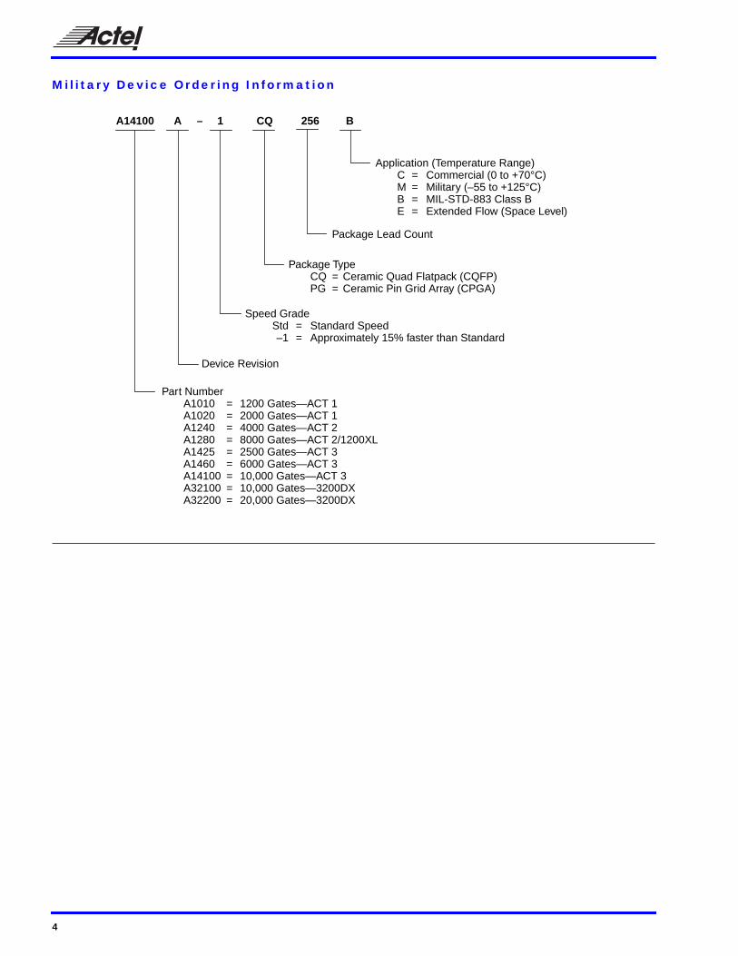
Military Device Ordering Information
Application (Temperature Range)C = Commercial (0 to +70°C)M = Military (–55 to +125°C)B = MIL-STD-883 Class BE = Extended Flow (Space Level)
Package TypeCQ = Ceramic Quad Flatpack (CQFP)PG = Ceramic Pin Grid Array (CPGA)
Speed GradeStd = Standard Speed–1 = Approximately 15% faster than Standard
Part NumberA1010 = 1200 Gates—ACT 1A1020 = 2000 Gates—ACT 1A1240 = 4000 Gates—ACT 2A1280 = 8000 Gates—ACT 2/1200XLA1425 = 2500 Gates—ACT 3A1460 = 6000 Gates—ACT 3A14100 = 10,000 Gates—ACT 3A32100 = 10,000 Gates—3200DXA32200 = 20,000 Gates—3200DX
Device Revision
Package Lead Count
A14100 CQ 256 B1A –
4

HiRel FPGAs
DESC SMD/Actel Part Number Cross Reference
Actel Part Number DSCC SMD DSCC SMD
(Gold Leads) (Gold Leads) (Solder Dipped)
A1010B-PG84B 5962-9096403MXC 5962-9096403MXA
A1010B-1PG84B 5962-9096404MXC 5962-9096404MXA
A1020B-PG84B 5962-9096503MUC 5962-9096503MUA
A1020B-1PG84B 5962-9096504MUC 5962-9096504MUA
A1020B-CQ84B 5962-9096503MTC 5962-9096503MTA
A1020B-1CQ84B 5962-9096504MTC 5962-9096504MTA
A1240A-PG132B 5962-9322101MXC 5962-9322101MXA
A1240A-1PG132B 5962-9322102MXC 5962-9322102MXA
A1280A-PG176B 5962-9215601MXC 5962-9215601MXA
A1280A-1PG176B 5962-9215602MXC 5962-9215602MXA
A1280A-CQ172B 5962-9215601MYC 5962-9215601MYA
A1280A-1CQ172B 5962-9215602MYC 5962-9215602MYA
A1425A-PG133B 5962-9552001MXC 5962-9552001MXA
A1425A-1PG133B 5962-9552002MXC 5962-9552002MXA
A1425A-CQ132B 5962-9552001MYC 5962-9552001MYA
A1425A-1CQ132B 5962-9552002MYC 5962-9552002MYA
A1460A-PG207B 5962-9550801MXC 5962-9550801MXA
A1460A-1PG207B 5962-9550802MXC 5962-9550802MXA
A1460A-CQ196B 5962-9550801MYC 5962-9550801MYA
A1460A-1CQ196B 5962-9550802MYC 5962-9550802MYA
A14100A-PG257B 5962-9552101MXC 5962-9552101MXA
A14100A-1PG257B 5962-9552102MXC 5962-9552102MXA
A14100A-CQ256B 5962-9552101MYC 5962-9552101MYA
A14100A-1CQ256B 5962-9552102MYC 5962-9552102MYA
A32100DX-CQ84B TBD TBD
A32100DX-1CQ84B TBD TBD
A32200DX-CQ208B TBD TBD
A32200DX-1CQ208B TBD TBD
5
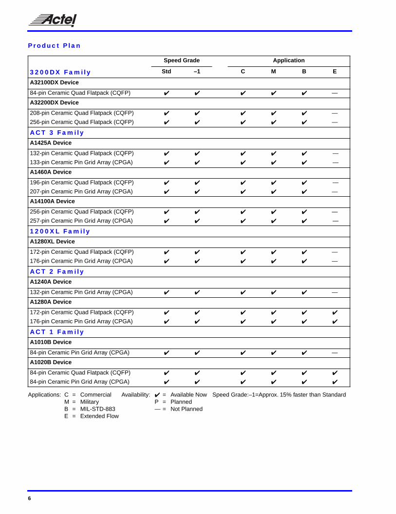
Product Plan
Applications: C = Commercial Availability: = Available Now Speed Grade:–1=Approx. 15% faster than StandardM = Military P = PlannedB = MIL-STD-883 — = Not PlannedE = Extended Flow
Speed Grade Application
3200DX Family Std –1 C M B E
A32100DX Device
84-pin Ceramic Quad Flatpack (CQFP) —
A32200DX Device
208-pin Ceramic Quad Flatpack (CQFP) —
256-pin Ceramic Quad Flatpack (CQFP) —
ACT 3 FamilyA1425A Device
132-pin Ceramic Quad Flatpack (CQFP) —
133-pin Ceramic Pin Grid Array (CPGA) —
A1460A Device
196-pin Ceramic Quad Flatpack (CQFP) —
207-pin Ceramic Pin Grid Array (CPGA) —
A14100A Device
256-pin Ceramic Quad Flatpack (CQFP) —
257-pin Ceramic Pin Grid Array (CPGA) —
1200XL FamilyA1280XL Device
172-pin Ceramic Quad Flatpack (CQFP) —
176-pin Ceramic Pin Grid Array (CPGA) —
ACT 2 FamilyA1240A Device
132-pin Ceramic Pin Grid Array (CPGA) —
A1280A Device
172-pin Ceramic Quad Flatpack (CQFP)
176-pin Ceramic Pin Grid Array (CPGA)
ACT 1 FamilyA1010B Device
84-pin Ceramic Pin Grid Array (CPGA) —
A1020B Device
84-pin Ceramic Quad Flatpack (CQFP)
84-pin Ceramic Pin Grid Array (CPGA)
6

HiRel FPGAs
3200DX Device Resources
ACT 3 Device Resources
1200XL Device Resources
ACT 2 Device Resources
ACT 1 Device Resources
Pin Description
CLK Clock (Input)
ACT 1 only. TTL Clock input for global clock distributionnetwork. The Clock input is buffered prior to clocking thelogic modules. This pin can also be used as an I/O.
CLKA Clock A (Input)
ACT 3, 1200XL, and ACT 2 only. TTL Clock input for globalclock distribution networks. The Clock input is buffered priorto clocking the logic modules. This pin can also be used as anI/O.
User I/Os
FPGA Device Type
Logic Modules
Gate Array Equivalent
Gates
CQFP
84-pin 208-pin 256-pin
A32100DX 1362 10,000 60 — —
A32200DX 2414 20,000 — 176 202
User I/Os
FPGA Device Type
Logic Modules
Gate Array Equivalent
Gates
CQFP CPGA
132-pin 196-pin 256-pin 133-pin 207-pin 257-pin
A1425A 310 2500 100 — — 100 — —
A1460A 848 6000 — 168 — — 168 —
A14100A 1377 10,000 — — 228 — — 228
User I/Os
FPGA Device Type
Logic Modules
Gate Array Equivalent
Gates
CQFP CPGA
172-pin 176-pin
A1280XL 1232 8000 140 140
User I/Os
FPGA Device Type
Logic Modules
Gate Array Equivalent
Gates
CQFP CPGA
172-pin 132-pin 176-pin
A1240A 684 4000 — 104 —
A1280A 1232 8000 140 — 140
User I/Os
FPGA Device Type
Logic Modules
Gate Array Equivalent
Gates
CQFP CPGA
84-pin 84-pin
A1010B 295 1200 — 57
A1020B 547 2000 69 69
7
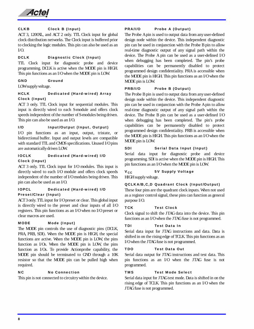
CLKB Clock B (Input)
ACT 3, 1200XL, and ACT 2 only. TTL Clock input for globalclock distribution networks. The Clock input is buffered priorto clocking the logic modules. This pin can also be used as anI/O.
DCLK Diagnostic Clock (Input)
TTL Clock input for diagnostic probe and deviceprogramming. DCLK is active when the MODE pin is HIGH.This pin functions as an I/O when the MODE pin is LOW.
GND Ground
LOW supply voltage.
HCLK Dedicated (Hard-wired) Array Clock (Input)
ACT 3 only. TTL Clock input for sequential modules. Thisinput is directly wired to each S-module and offers clockspeeds independent of the number of S-modules being driven.This pin can also be used as an I/O.
I/O Input/Output (Input, Output)
I/O pin functions as an input, output, tristate, orbidirectional buffer. Input and output levels are compatiblewith standard TTL and CMOS specifications. Unused I/O pinsare automatically driven LOW.
IOCLK Dedicated (Hard-wired) I/O Clock (Input)
ACT 3 only. TTL Clock input for I/O modules. This input isdirectly wired to each I/O module and offers clock speedsindependent of the number of I/O modules being driven. Thispin can also be used as an I/O.
IOPCL Dedicated (Hard-wired) I/O Preset/Clear (Input)
ACT 3 only. TTL input for I/O preset or clear. This global inputis directly wired to the preset and clear inputs of all I/Oregisters. This pin functions as an I/O when no I/O preset orclear macros are used.
MODE Mode (Input)
The MODE pin controls the use of diagnostic pins (DCLK,PRA, PRB, SDI). When the MODE pin is HIGH, the specialfunctions are active. When the MODE pin is LOW, the pinsfunction as I/Os. When the MODE pin is LOW, the pinsfunction as I/Os. To provide Actionprobe capability, theMODE pin should be terminated to GND through a 10Kresistor so that the MODE pin can be pulled high whenrequired.
NC No Connection
This pin is not connected to circuitry within the device.
PRA/I/O Probe A (Output)
The Probe A pin is used to output data from any user-defineddesign node within the device. This independent diagnosticpin can be used in conjunction with the Probe B pin to allowreal-time diagnostic output of any signal path within thedevice. The Probe A pin can be used as a user-defined I/Owhen debugging has been completed. The pin’s probecapabilities can be permanently disabled to protectprogrammed design confidentiality. PRA is accessible whenthe MODE pin is HIGH. This pin functions as an I/O when theMODE pin is LOW.
PRB/I/O Probe B (Output)
The Probe B pin is used to output data from any user-defineddesign node within the device. This independent diagnosticpin can be used in conjunction with the Probe A pin to allowreal-time diagnostic output of any signal path within thedevice. The Probe B pin can be used as a user-defined I/Owhen debugging has been completed. The pin's probecapabilities can be permanently disabled to protectprogrammed design confidentiality. PRB is accessible whenthe MODE pin is HIGH. This pin functions as an I/O when theMODE pin is LOW.
SDI Serial Data Input (Input)
Serial data input for diagnostic probe and deviceprogramming. SDI is active when the MODE pin is HIGH. Thispin functions as an I/O when the MODE pin is LOW.
VCC 5V Supply Voltage
HIGH supply voltage.
QCLKA/B,C,D Quadrant Clock (Input/Output)
These four pins are the quadrant clock inputs. When not usedas a register control signal, these pins can function as generalpurpose I/O.
TCK Test Clock
Clock signal to shift the JTAG data into the device. This pinfunctions as an I/O when the JTAG fuse is not programmed.
TDI Test Data In
Serial data input for JTAG instructions and data. Data isshifted in on the rising edge of TCLK. This pin functions as anI/O when the JTAG fuse is not programmed.
TDO Test Data Out
Serial data output for JTAG instructions and test data. Thispin functions as an I/O when the JTAG fuse is notprogrammed.
TMS Test Mode Select
Serial data input for JTAG test mode. Data is shifted in on therising edge of TCLK. This pin functions as an I/O when theJTAG fuse is not programmed.
8
HiRel FPGAs
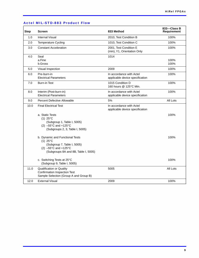
Actel MIL-STD-883 Product Flow
Step Screen 833 Method833—Class BRequirement
1.0 Internal Visual 2010, Test Condition B 100%
2.0 Temperature Cycling 1010, Test Condition C 100%
3.0 Constant Acceleration 2001, Test Condition E(min), Y1, Orientation Only
100%
4.0 Seala.Fineb.Gross
1014100%100%
5.0 Visual Inspection 2009 100%
6.0 Pre-burn-inElectrical Parameters
In accordance with Actel applicable device specification
100%
7.0 Burn-in Test 1015 Condition D160 hours @ 125°C Min.
100%
8.0 Interim (Post-burn-in)Electrical Parameters
In accordance with Actel applicable device specification
100%
9.0 Percent Defective Allowable 5% All Lots
10.0 Final Electrical Test
a. Static Tests(1) 25°C
(Subgroup 1, Table I, 5005)(2) –55°C and +125°C
(Subgroups 2, 3, Table I, 5005)
b. Dynamic and Functional Tests(1) 25°C
(Subgroup 7, Table I, 5005)(2) –55°C and +125°C
(Subgroups 8A and 8B, Table I, 5005)
c. Switching Tests at 25°C(Subgroup 9, Table I, 5005)
In accordance with Actel applicable device specification
100%
100%
100%
11.0 Qualification or Quality Confirmation Inspection Test Sample Selection (Group A and Group B)
5005 All Lots
12.0 External Visual 2009 100%
9
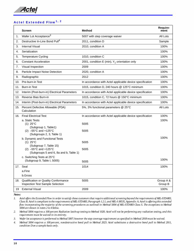
Actel Extended Flow1, 2
Notes:1. Actel offers the Extended Flow in order to satisfy those customers that require additional screening beyond the requirements of MIL-STD-883,
Class B. Actel is compliant to the requirements of MIL-STD-883, Paragraph 1.2.1, and MIL-I-38535, Appendix A. Actel is offering this extendedflow incorporating the majority of the screening procedures as outlined in Method 5004 of MIL-STD-883 Class S. The exceptions to Method5004 are shown in notes 2 to 4 below.
2. Method 5004 requires a 100 percent Radiation latch-up testing to Method 1020. Actel will not be performing any radiation testing, and thisrequirement must be waived in its entirety.
3. Wafer lot acceptance is performed to Method 5007; however the step coverage requirement as specified in Method 2018 must be waived.4. Method 5004 requires a 100 percent, nondestructive bond pull to Method 2023. Actel substitutes a destructive bond pull to Method 2011,
condition D on a sample basis only.
Screen MethodRequire-
ment
1. Wafer Lot Acceptance3 5007 with step coverage waiver All Lots
2. Destructive In-Line Bond Pull4 2011, condition D Sample
3. Internal Visual 2010, condition A 100%
4. Serialization 100%
5. Temperature Cycling 1010, condition C 100%
6. Constant Acceleration 2001, condition E (min), Y1 orientation only 100%
7. Visual Inspection 2009 100%
8. Particle Impact Noise Detection 2020, condition A 100%
9. Radiographic 2012 100%
10. Pre-burn-in Test In accordance with Actel applicable device specification 100%
11. Burn-in Test 1015, condition D, 240 hours @ 125°C minimum 100%
12. Interim (Post-burn-in) Electrical Parameters In accordance with Actel applicable device specification 100%
13. Reverse Bias Burn-in 1015, condition C, 72 hours @ 150°C minimum 100%
14. Interim (Post-burn-in) Electrical Parameters In accordance with Actel applicable device specification 100%
15. Percent Defective Allowable (PDA) Calculation
5%, 3% functional parameters @ 25°C All Lots
16. Final Electrical Test
a. Static Tests(1) 25°C
(Subgroup 1, Table1)(2) –55°C and +125°C
(Subgroups 2, 3, Table 1)
b. Dynamic and Functional Tests(1) 25°C
(Subgroup 7, Table 15)(2) –55°C and +125°C
(Subgroups 5 and 6, 8a and b, Table 1)
c. Switching Tests at 25°C(Subgroup 9, Table I, 5005)
In accordance with Actel applicable device specification
5005
5005
5005
5005
5005
100%
100%
100%
100%
17. Seal
a.Fine
b.Gross
1014 100%
18. Qualification or Quality Conformance Inspection Test Sample Selection
5005 Group A & Group B
19 External Visual 2009 100%
10
HiRel FPGAs
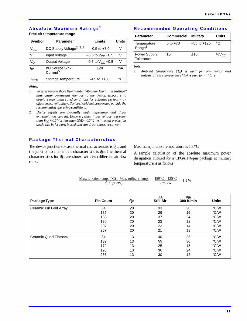
Absolute Maximum Ratings1
Free air temperature range
Notes:1. Stresses beyond those listed under “Absolute Maximum Ratings”
may cause permanent damage to the device. Exposure toabsolute maximum rated conditions for extended periods mayaffect device reliability. Device should not be operated outside therecommended operating conditions.
2. Device inputs are normally high impedance and drawextremely low current. However, when input voltage is greaterthan VCC + 0.5 V or less than GND – 0.5 V, the internal protectiondiode will be forward biased and can draw excessive current.
Recommended Operating Conditions
Note:1. Ambient temperature (TA) is used for commercial and
industrial; case temperature (TC) is used for military.
Package Thermal Characteristics
The device junction to case thermal characteristic is θjc, andthe junction to ambient air characteristic is θja. The thermalcharacteristics for θja are shown with two different air flowrates.
Maximum junction temperature is 150°C.
A sample calculation of the absolute maximum powerdissipation allowed for a CPGA 176-pin package at militarytemperature is as follows:
Symbol Parameter Limits Units
VCC DC Supply Voltage2, 3, 4 –0.5 to +7.0 V
VI Input Voltage –0.5 to VCC +0.5 V
VO Output Voltage –0.5 to VCC +0.5 V
IIO I/O Source SinkCurrent5
±20 mA
TSTG Storage Temperature –65 to +150 °C
Parameter Commercial Military Units
Temperature Range1
0 to +70 –55 to +125 °C
Power Supply Tolerance
±5 ±10 %VCC
Package Type Pin Count θjcθja
Still Airθja
300 ft/min Units
Ceramic Pin Grid Array 84132133176207257
202020202020
332637232221
201624121413
°C/W°C/W°C/W°C/W°C/W°C/W
Ceramic Quad Flatpack 84132172196256
1313131313
4055253630
2530152418
°C/W°C/W°C/W°C/W°C/W
Max. junction temp. (°C) – Max. military temp. θ
ja (°C/W)
------------------------------------------------------------------------------------------------------------------ 150°C – 125°C23°C/W
------------------------------------ 1.1 W= =
11
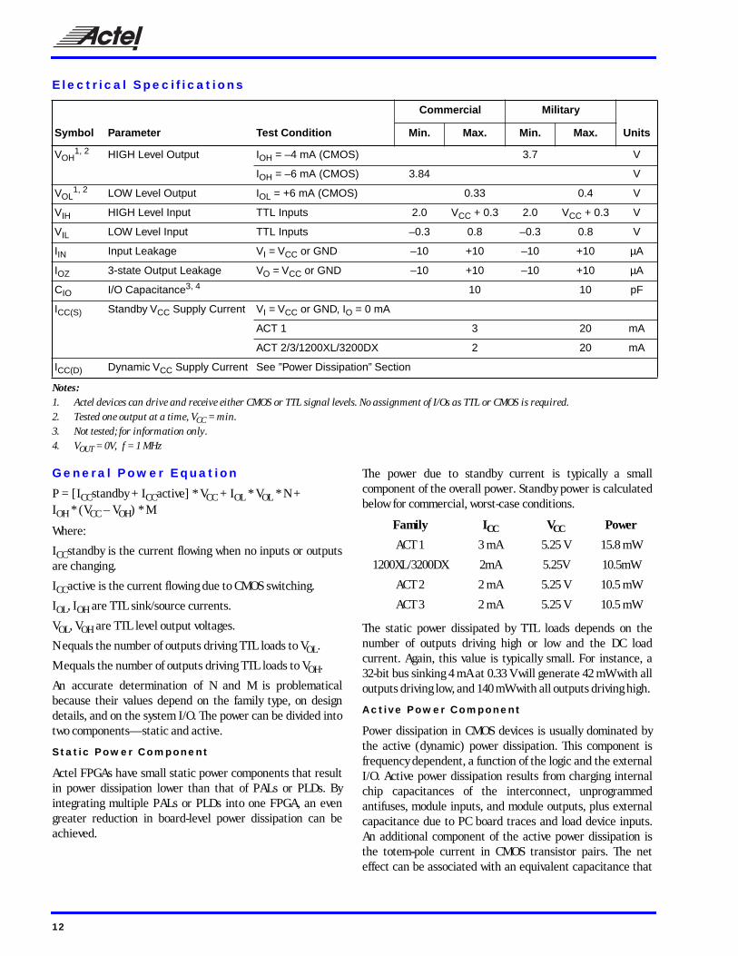
Electrical Specifications
Notes:
1. Actel devices can drive and receive either CMOS or TTL signal levels. No assignment of I/Os as TTL or CMOS is required.2. Tested one output at a time, V
CC
= min.3. Not tested; for information only.4. V
OUT
= 0V, f = 1 MHz
General Power Equation
P = [I
CC
standby + I
CC
active] * V
CC
+ I
OL
* V
OL
* N + I
OH
* (V
CC
– V
OH
) * M
Where:
I
CC
standby is the current flowing when no inputs or outputs
are changing.
I
CC
active is the current flowing due to CMOS switching.
I
OL
, I
OH
are TTL sink/source currents.
V
OL
, V
OH
are TTL level output voltages.
N equals the number of outputs driving TTL loads to VOL.
M equals the number of outputs driving TTL loads to VOH.
An accurate determination of N and M is problematicalbecause their values depend on the family type, on designdetails, and on the system I/O. The power can be divided intotwo components—static and active.
Static Power Component
Actel FPGAs have small static power components that resultin power dissipation lower than that of PALs or PLDs. Byintegrating multiple PALs or PLDs into one FPGA, an evengreater reduction in board-level power dissipation can beachieved.
The power due to standby current is typically a smallcomponent of the overall power. Standby power is calculatedbelow for commercial, worst-case conditions.
The static power dissipated by TTL loads depends on thenumber of outputs driving high or low and the DC loadcurrent. Again, this value is typically small. For instance, a32-bit bus sinking 4 mA at 0.33 V will generate 42 mW with alloutputs driving low, and 140 mW with all outputs driving high.
Active Power Component
Power dissipation in CMOS devices is usually dominated bythe active (dynamic) power dissipation. This component isfrequency dependent, a function of the logic and the externalI/O. Active power dissipation results from charging internalchip capacitances of the interconnect, unprogrammedantifuses, module inputs, and module outputs, plus externalcapacitance due to PC board traces and load device inputs.An additional component of the active power dissipation isthe totem-pole current in CMOS transistor pairs. The neteffect can be associated with an equivalent capacitance that
Symbol Parameter Test Condition
Commercial Military
UnitsMin. Max. Min. Max.
VOH1, 2 HIGH Level Output IOH = –4 mA (CMOS) 3.7 V
IOH = –6 mA (CMOS) 3.84 V
VOL1, 2 LOW Level Output IOL = +6 mA (CMOS) 0.33 0.4 V
VIH HIGH Level Input TTL Inputs 2.0 VCC + 0.3 2.0 VCC + 0.3 V
VIL LOW Level Input TTL Inputs –0.3 0.8 –0.3 0.8 V
IIN Input Leakage VI = VCC or GND –10 +10 –10 +10 µA
IOZ 3-state Output Leakage VO = VCC or GND –10 +10 –10 +10 µA
CIO I/O Capacitance3, 4 10 10 pF
ICC(S) Standby VCC Supply Current VI = VCC or GND, IO = 0 mA
ACT 1 3 20 mA
ACT 2/3/1200XL/3200DX 2 20 mA
ICC(D) Dynamic VCC Supply Current See ”Power Dissipation” Section
Family ICC VCC Power
ACT 1 3 mA 5.25 V 15.8 mW
1200XL/3200DX 2mA 5.25V 10.5mW
ACT 2 2 mA 5.25 V 10.5 mW
ACT 3 2 mA 5.25 V 10.5 mW
12
HiRel FPGAs
can be combined with frequency and voltage to representactive power dissipation.
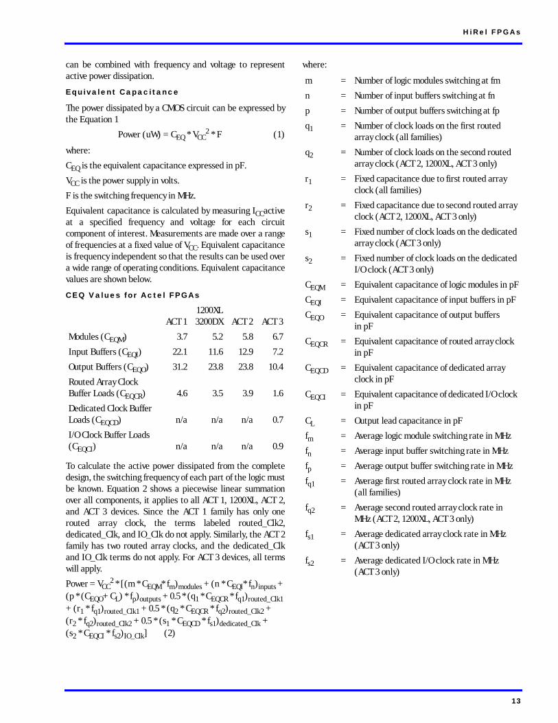
Equivalent Capacitance
The power dissipated by a CMOS circuit can be expressed bythe Equation 1
Power (uW) = CEQ * VCC2 * F (1)
where:
CEQ is the equivalent capacitance expressed in pF.
VCC is the power supply in volts.
F is the switching frequency in MHz.
Equivalent capacitance is calculated by measuring ICCactiveat a specified frequency and voltage for each circuitcomponent of interest. Measurements are made over a rangeof frequencies at a fixed value of VCC. Equivalent capacitanceis frequency independent so that the results can be used overa wide range of operating conditions. Equivalent capacitancevalues are shown below.
CEQ Values for Actel FPGAs
To calculate the active power dissipated from the completedesign, the switching frequency of each part of the logic mustbe known. Equation 2 shows a piecewise linear summationover all components, it applies to all ACT 1, 1200XL, ACT 2,and ACT 3 devices. Since the ACT 1 family has only onerouted array clock, the terms labeled routed_Clk2,dedicated_Clk, and IO_Clk do not apply. Similarly, the ACT 2family has two routed array clocks, and the dedicated_Clkand IO_Clk terms do not apply. For ACT 3 devices, all termswill apply.
Power = VCC2 * [(m * CEQM* fm)modules + (n * CEQI* fn)inputs +
(p * (CEQO+ CL) * fp)outputs + 0.5 * (q1 * CEQCR * fq1)routed_Clk1 + (r1 * fq1)routed_Clk1 + 0.5 * (q2 * CEQCR * fq2)routed_Clk2 + (r2 * fq2)routed_Clk2 + 0.5 * (s1 * CEQCD * fs1)dedicated_Clk + (s2 * CEQCI * fs2)IO_Clk] (2)
where:
ACT 11200XL3200DX ACT 2 ACT 3
Modules (CEQM) 3.7 5.2 5.8 6.7
Input Buffers (CEQI) 22.1 11.6 12.9 7.2
Output Buffers (CEQO) 31.2 23.8 23.8 10.4
Routed Array Clock Buffer Loads (CEQCR) 4.6 3.5 3.9 1.6
Dedicated Clock Buffer Loads (CEQCD) n/a n/a n/a 0.7
I/O Clock Buffer Loads (CEQCI) n/a n/a n/a 0.9
m = Number of logic modules switching at fm
n = Number of input buffers switching at fn
p = Number of output buffers switching at fp
q1 = Number of clock loads on the first routed array clock (all families)
q2 = Number of clock loads on the second routed array clock (ACT 2, 1200XL, ACT 3 only)
r1 = Fixed capacitance due to first routed array clock (all families)
r2 = Fixed capacitance due to second routed array clock (ACT 2, 1200XL, ACT 3 only)
s1 = Fixed number of clock loads on the dedicated array clock (ACT 3 only)
s2 = Fixed number of clock loads on the dedicated I/O clock (ACT 3 only)
CEQM = Equivalent capacitance of logic modules in pF
CEQI = Equivalent capacitance of input buffers in pF
CEQO = Equivalent capacitance of output buffers in pF
CEQCR = Equivalent capacitance of routed array clock in pF
CEQCD = Equivalent capacitance of dedicated array clock in pF
CEQCI = Equivalent capacitance of dedicated I/O clock in pF
CL = Output lead capacitance in pF
fm = Average logic module switching rate in MHz
fn = Average input buffer switching rate in MHz
fp = Average output buffer switching rate in MHz
fq1 = Average first routed array clock rate in MHz (all families)
fq2 = Average second routed array clock rate in MHz (ACT 2, 1200XL, ACT 3 only)
fs1 = Average dedicated array clock rate in MHz (ACT 3 only)
fs2 = Average dedicated I/O clock rate in MHz(ACT 3 only)
13

Fixed Capacitance Values for Actel FPGAs (pF)
Fixed Clock Loads (s1/s2—ACT 3 Only)
Determining Average Switching Frequency
To determine the switching frequency for a design, you musthave a detailed understanding of the data values input to thecircuit. The guidelines in the table below are meant torepresent worst-case scenarios so that they can be generallyused to predict the upper limits of power dissipation.
Device Typer1
routed_Clk1r2
routed_Clk2
A1010B 41 n/a
A1020B 69 n/a
A1240A 134 134
A1280A 168 168
A1280XL 168 168
A1425A 75 75
A1460A 165 165
A14100A 195 195
A32100DX 178 178
A32200DX 230 230
Device Type
s1Clock Loads on
DedicatedArray Clock
s2Clock Loads on
DedicatedI/O Clock
A1425A 160 100
A1460A 432 168
A14100A 697 228
Type ACT 1 ACT 2/1200XL/3200DX ACT 3
Logic modules (m) 90% of modules 80% of modules 80% of modules
Input switching (n) # inputs/4 # inputs/4 # inputs/4
Outputs switching (p) #outputs/4 #outputs/4 #outputs/4
First routed array clock loads (q1) 40% of modules 40% of sequential modules
40% of sequential modules
Second routed array clock loads (q2) n/a 40% of sequential modules
40% of sequential modules
Load capacitance (CL) 35 pF 35 pF 35 pF
Average logic module switching rate (fm) F/10 F/10 F/10
Average input switching rate (fn) F/5 F/5 F/5
Average output switching rate (fp) F/10 F/10 F/10
Average first routed array clock rate (fq1) F F F/2
Average second routed array clock rate (fq2) n/a F/2 F/2
Average dedicated array clock rate (fs1) n/a n/a F
Average dedicated I/O clock rate (fs2) n/a n/a F
14

HiRel FPGAs
1200XL Timing Model*
*Values shown for A1280XL-1 at worst-case military conditions. † Input Module Predicted Routing Delay
Output DelaysInternal DelaysInput Delays
tINH = 0.0 nstINSU = 0.4 ns
I/O Module
D Q
tINGL = 3.7 ns
tINYL = 1.7 ns tIRD2 = 5.2 ns†
CombinatorialLogic Module
tPD = 3.7 ns
SequentialLogic Module
I/O Module
tRD1 = 1.7 nstDLH = 6.6 ns
I/O Module
ARRAYCLOCKS
FMAX = 110 MHz
Combin-atorial Logicincluded in tSUD
D Q D Q
tOUTH = 0.0 nstOUTSU = 0.4 ns
tGLH = 5.9 ns
tDLH = 6.6 ns
tENHZ = 7.5 nstRD1 = 1.7 ns
tCO = 3.7 nstSU = 0.4 nstHD = 0.0 ns
tRD4 = 3.7 nstRD8 = 7.0 ns
PredictedRoutingDelays
tCKH = 7.1 ns
G
G
FO = 256
tRD2 = 2.5 ns
tLCO = 10.7 ns (64 loads, pad-pad)
15
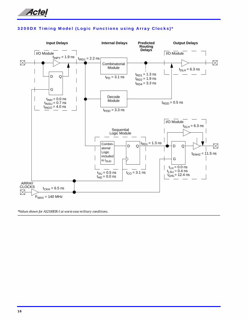
3200DX Timing Model (Logic Functions using Array Clocks)*
*Values shown for A32100DX-1 at worst-case military conditions.
Output DelaysInternal DelaysInput Delays
tINH = 0.0 nstINSU = 0.7 ns
I/O Module
D Q
tINGO = 4.0 ns
tINPY = 1.9 ns tIRD1 = 2.2 ns
CombinatorialModule
tPD = 3.1 ns
SequentialLogic Module
I/O Module
tRD1 = 1.3 nstDLH = 6.3 ns
I/O Module
ARRAYCLOCKS
FMAX = 140 MHz
Combin-atorial Logicincluded in tSUD
D Q D Q
tLH = 0.0 nstLSU = 0.4 nstGHL= 12.4 ns
tDLH = 6.3 ns
tENHZ = 11.5 ns
tRD1 = 1.3 ns
tCO = 3.1 nstSU = 0.5 nstHD = 0.0 ns
PredictedRoutingDelays
G
G
DecodeModule
tPDD = 3.3 ns
tRDD = 0.5 ns
tRD2 = 1.9 nstRD4 = 3.3 ns
tCKH = 6.5 ns
16
HiRel FPGAs
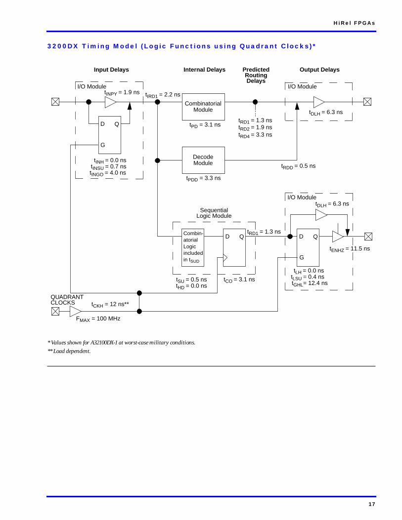
3200DX Timing Model (Logic Functions using Quadrant Clocks)*
* Values shown for A32100DX-1 at worst-case military conditions.
** Load dependent.
Output DelaysInternal DelaysInput Delays
tINH = 0.0 nstINSU = 0.7 ns
I/O Module
D Q
tINGO = 4.0 ns
tINPY = 1.9 ns tIRD1 = 2.2 ns
CombinatorialModule
tPD = 3.1 ns
SequentialLogic Module
I/O Module
tRD1 = 1.3 nstDLH = 6.3 ns
I/O Module
QUADRANTCLOCKS
FMAX = 100 MHz
Combin-atorial Logicincluded in tSUD
D Q D Q
tLH = 0.0 nstLSU = 0.4 nstGHL= 12.4 ns
tDLH = 6.3 ns
tENHZ = 11.5 ns
tRD1 = 1.3 ns
tCO = 3.1 nstSU = 0.5 nstHD = 0.0 ns
PredictedRoutingDelays
G
G
DecodeModule
tPDD = 3.3 ns
tRDD = 0.5 ns
tRD2 = 1.9 nstRD4 = 3.3 ns
tCKH = 12 ns**
17
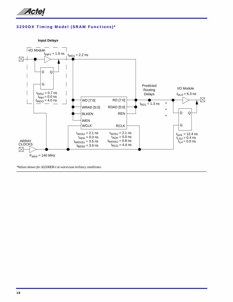
3200DX Timing Model (SRAM Functions)*
*Values shown for A32100DX-1 at worst-case military conditions.
tINH = 0.0 nstINSU = 0.7 ns
Input Delays
I/O Module
D Q
tINGO = 4.0 ns
tINPY = 1.9 ns tIRD1 = 2.2 ns
ARRAYCLOCKS
FMAX = 140 MHz
G
tGHL = 12.4 nstLSU = 0.4 ns
I/O Module
D Q
tLH = 0.0 ns
tDLH = 6.3 ns
G
WD [7:0]
WRAD [5:0]
BLKEN
WEN
WCLK
tADSU = 2.1 nstADH = 0.0 ns
tWENSU = 3.5 nstBENS = 3.6 ns
RD [7:0]
RDAD [5:0]
REN
RCLK
tADSU = 2.1 nstADH = 0.0 ns
tRENSU = 0.8 ns
•
•
•
tRD1 = 1.3 ns
Predicted Routing Delays
tRCO = 4.4 ns
18
HiRel FPGAs
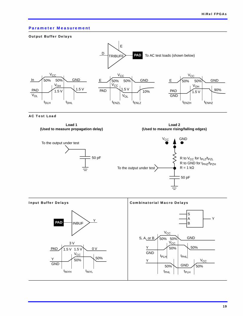
Parameter Measurement
Output Buffer Delays
AC Test Load
Input Buffer Delays Combinatorial Macro Delays
PAD To AC test loads (shown below)D
E
TRIBUFF
In
VCC
GND50%
PADVOL
VOH
1.5 V
tDLH
50%
1.5 V
tDHL
E
VCC
GND50%
PADVOL
1.5 V
tENZL
50%
10%
tENLZ
E
VCC
GND50%
PADGND
VOH
1.5 V
tENZH
50%
90%
tENHZ
VCC
PAD
Load 1(Used to measure propagation delay)
Load 2(Used to measure rising/falling edges)
50 pF
To the output under testVCC GND
50 pF
To the output under test
R to VCC for tPLZ/tPZLR to GND for tPHZ/tPZHR = 1 kΩ
PADY
INBUF
PAD
3 V
0 V1.5 V
YGND
VCC
50%
tINYH
1.5 V
50%
tINYL
PAD
SAB
Y
S, A, or B
Y
GND
VCC
50%
tPLH
Y
GND
GND
VCC
50%
50% 50%
VCC
50% 50%tPHL
tPHLtPLH
19
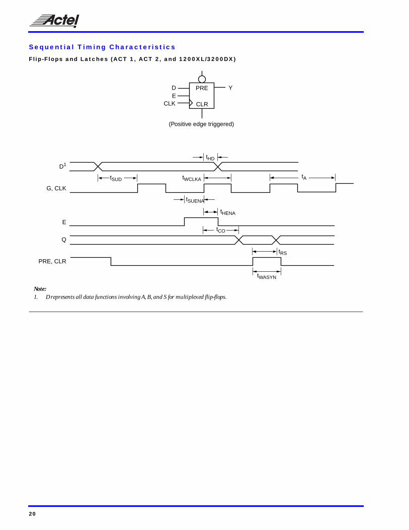
Sequential Timing Characteristics
Flip-Flops and Latches (ACT 1, ACT 2, and 1200XL/3200DX)
(Positive edge triggered)
DE
CLK CLR
PRE Y
D1
G, CLK
E
Q
PRE, CLR
tWCLKA
tWASYN
tHD
tSUENA
tSUD
tRS
tA
tCO
tHENA
Note:1. D represents all data functions involving A, B, and S for multiplexed flip-flops.
20
HiRel FPGAs
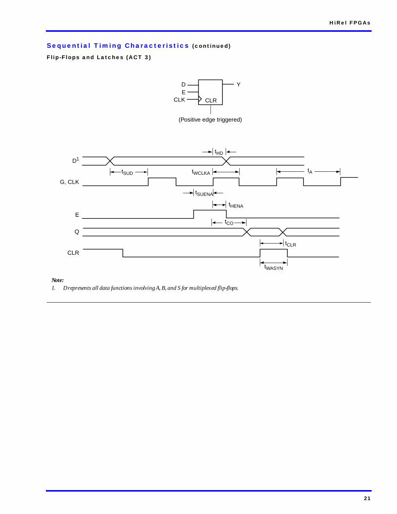
Sequential Timing Characteristics (continued)
Flip-Flops and Latches (ACT 3)
(Positive edge triggered)
DE
CLK CLR
Y
D1
G, CLK
E
Q
CLR
tWCLKA
tWASYN
tHD
tSUENA
tSUD
tCLR
tA
tCO
tHENA
Note:1. D represents all data functions involving A, B, and S for multiplexed flip-flops.
21
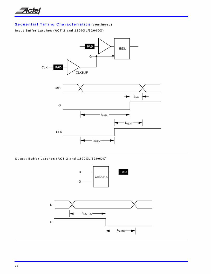
Sequential Timing Characteristics (continued)
Input Buffer Latches (ACT 2 and 1200XL/3200DX)
Output Buffer Latches (ACT 2 and 1200XL/3200DX)
G
PAD
PADCLK
PAD
G
CLK
tINH
CLKBUF
tINSU
tSUEXT
tHEXT
IBDL
D
G
tOUTSU
tOUTH
PAD
OBDLHS
D
G
22
HiRel FPGAs
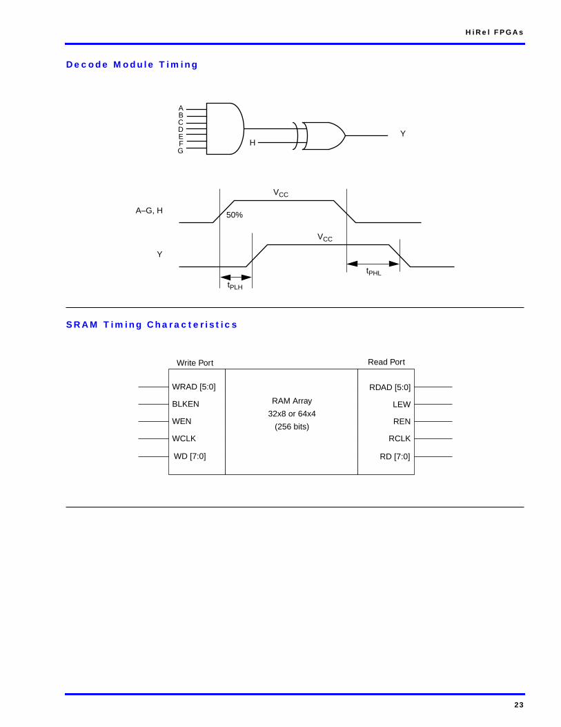
Decode Module Timing
SRAM Timing Characteristics
A–G, H
Y
tPLH
50%
VCC
VCC
tPHL
Y
ABCDEFG
H
WRAD [5:0]
BLKEN
WEN
WCLK
RDAD [5:0]
LEW
REN
RCLK
RD [7:0]WD [7:0]
Write Port Read Port
RAM Array
32x8 or 64x4
(256 bits)
23
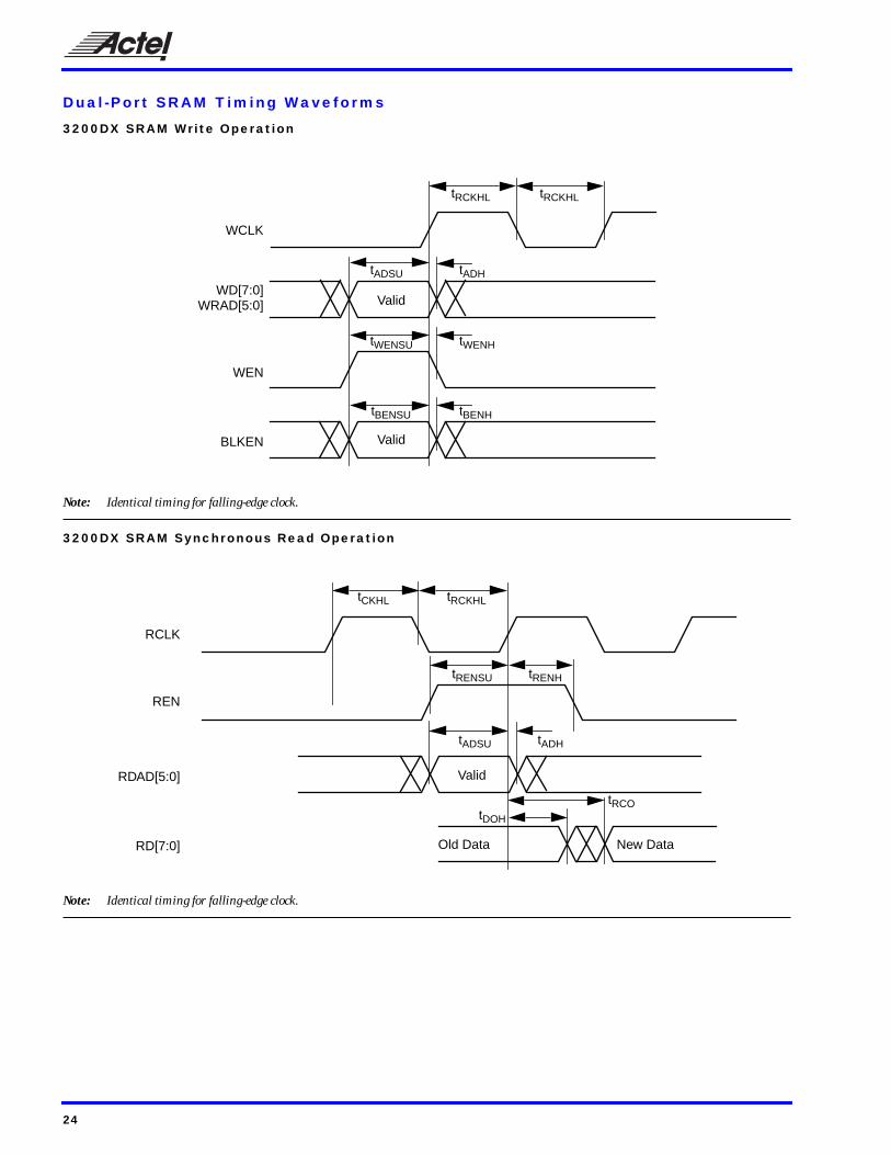
Dual-Port SRAM Timing Waveforms
3200DX SRAM Write Operation
3200DX SRAM Synchronous Read Operation
Note: Identical timing for falling-edge clock.
WCLK
WD[7:0]WRAD[5:0]
WEN
BLKEN Valid
Valid
tRCKHLtRCKHL
tWENSU
tBENSU
tWENH
tBENH
tADSU tADH
Note: Identical timing for falling-edge clock.
RCLK
REN
RDAD[5:0]
RD[7:0] Old Data
Valid
tRCKHLtCKHL
tRENH
tRCO
tADH
tDOH
tADSU
New Data
tRENSU
24
HiRel FPGAs
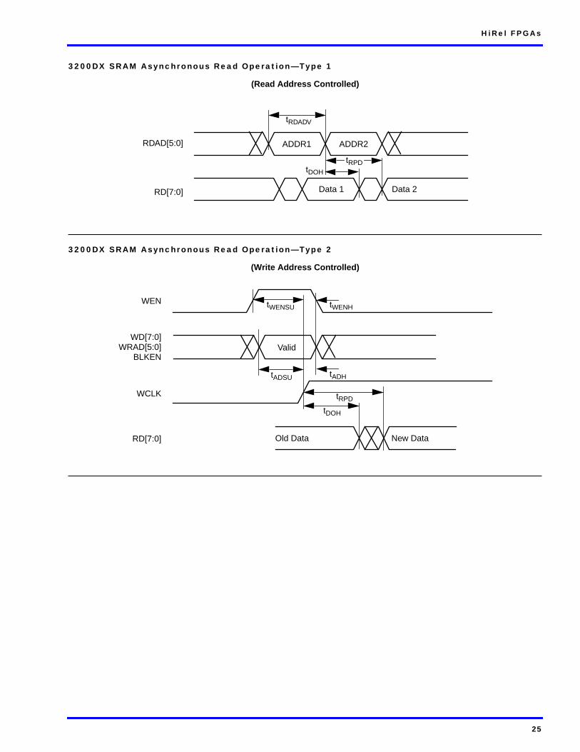
3200DX SRAM Asynchronous Read Operation—Type 1
3200DX SRAM Asynchronous Read Operation—Type 2
(Read Address Controlled)
(Write Address Controlled)
RDAD[5:0]
RD[7:0] Data 1
tRDADV
tDOH
ADDR2ADDR1
Data 2
tRPD
WEN
WD[7:0]
WCLK
RD[7:0] Old Data
Valid
tWENH
tRPD
tWENSU
New Data
tDOH
tADSU
WRAD[5:0]BLKEN
tADH
25

ACT 1 Timing Characteristics
(Worst-Case Military Conditions)
Notes:1. Routing delays are for typical designs across worst-case operating conditions. These parameters should be used for estimating device
performance. Post-route timing analysis or simulation is required to determine actual worst-case performance. Post-route timing is basedon actual routing delay measurements performed on the device prior to shipment.
2. Setup times assume fanout of 3. Further derating information can be obtained from the DirectTime Analyzer utility.
Logic Module Propagation Delays –1 Speed Std Speed
Parameter Description Min. Max. Min. Max. Units
tPD1 Single Module 4.7 5.5 ns
tPD2 Dual Module Macros 10.8 12.7 ns
tCO Sequential Clk to Q 4.7 5.5 ns
tGO Latch G to Q 4.7 5.5 ns
tRS Flip-Flop (Latch) Reset to Q 4.7 5.5 ns
Predicted Routing Delays 1
tRD1 FO=1 Routing Delay 1.5 1.7 ns
tRD2 FO=2 Routing Delay 2.3 2.7 ns
tRD3 FO=3 Routing Delay 3.4 4.0 ns
tRD4 FO=4 Routing Delay 5.0 5.9 ns
tRD8 FO=8 Routing Delay 10.6 12.5 ns
Sequential Timing Characteristics 2
tSUD Flip-Flop (Latch) Data Input Setup 8.8 10.4 ns
tHD Flip-Flop (Latch) Data Input Hold 0.0 0.0 ns
tSUENA Flip-Flop (Latch) Enable Setup 8.8 10.4 ns
tHENA Flip-Flop (Latch) Enable Hold 0.0 0.0 ns
tWCLKA Flip-Flop (Latch) Clock Active Pulse Width 10.9 12.9 ns
tWASYN Flip-Flop (Latch) Asynchronous Pulse Width 10.9 12.9 ns
tA Flip-Flop Clock Input Period 23.2 27.3 ns
fMAX Flip-Flop (Latch) Clock Frequency 44 37 MHz
26

HiRel FPGAs
ACT 1 Timing Characteristics (continued)
(Worst-Case Military Conditions)
Note:1. These parameters should be used for estimating device performance. Routing delays are for typical designs across worst-case operating
conditions. Post-route timing analysis or simulation is required to determine actual worst-case performance. Post-route timing is based onactual routing delay measurements performed on the device prior to shipment.
Input Module Propagation Delays –1 Speed Std Speed
Parameter Description Min. Max. Min. Max. Units
tINYH Pad to Y High 4.9 5.8 ns
tINYL Pad to Y Low 4.9 5.8 ns
Input Module Predicted Routing Delays 1
tIRD1 FO=1 Routing Delay 1.5 1.7 ns
tIRD2 FO=2 Routing Delay 2.3 2.7 ns
tIRD3 FO=3 Routing Delay 3.4 4.0 ns
tIRD4 FO=4 Routing Delay 5.0 5.9 ns
tIRD8 FO=8 Routing Delay 10.6 12.5 ns
Global Clock Network
tCKH Input Low to HighFO = 16FO = 128
7.88.9
9.210.5
ns
tCKL Input High to LowFO = 16FO = 128
10.311.2
12.113.2
ns
tPWH Minimum Pulse Width HighFO = 16FO = 128
10.410.9
12.212.9
ns
tPWL Minimum Pulse Width LowFO = 16FO = 128
10.410.9
12.212.9
ns
tCKSW Maximum SkewFO = 16FO = 128
1.92.9
2.23.4
ns
tP Minimum PeriodFO = 16FO = 128
21.723.2
25.627.3
ns
fMAX Maximum FrequencyFO = 16FO = 128
4644
4037
MHz
27

ACT 1 Timing Characteristics (continued)
(Worst-Case Military Conditions)
Notes:1. Delays based on 50 pF loading.2. SSO information can be found in the “Simultaneously Switching Output Limits for Actel FPGAs” application note.
Output Module Timing –1 Speed Std Speed
Parameter Description Min. Max. Min. Max. Units
TTL Output Module Timing 1
tDLH Data to Pad High 12.1 14.2 ns
tDHL Data to Pad Low 13.8 16.3 ns
tENZH Enable Pad Z to High 12.0 14.1 ns
tENZL Enable Pad Z to Low 14.6 17.1 ns
tENHZ Enable Pad High to Z 16.0 18.8 ns
tENLZ Enable Pad Low to Z 14.5 17.0 ns
dTLH Delta Low to High 0.09 0.11 ns/pF
dTHL Delta High to Low 0.12 0.15 ns/pF
CMOS Output Module Timing 1
tDLH Data to Pad High 15.1 17.7 ns
tDHL Data to Pad Low 11.5 13.6 ns
tENZH Enable Pad Z to High 12.0 14.1 ns
tENZL Enable Pad Z to Low 14.6 17.1 ns
tENHZ Enable Pad High to Z 16.0 18.8 ns
tENLZ Enable Pad Low to Z 14.5 17.0 ns
dTLH Delta Low to High 0.16 0.18 ns/pF
dTHL Delta High to Low 0.09 0.11 ns/pF
28
HiRel FPGAs
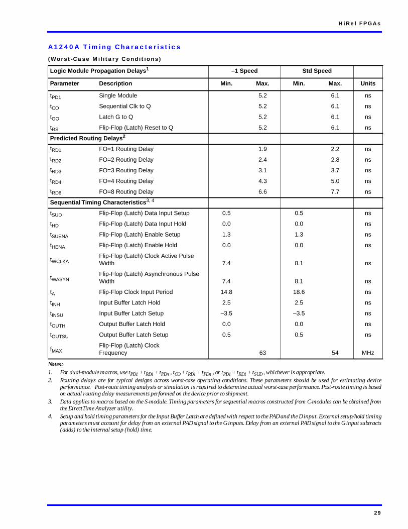
A1240A Timing Characteristics
(Worst-Case Military Conditions)
Notes:1. For dual-module macros, use tPD1 + tRD1 + tPDn , tCO + tRD1 + tPDn , or tPD1 + tRD1 + tSUD , whichever is appropriate.2. Routing delays are for typical designs across worst-case operating conditions. These parameters should be used for estimating device
performance. Post-route timing analysis or simulation is required to determine actual worst-case performance. Post-route timing is basedon actual routing delay measurements performed on the device prior to shipment.
3. Data applies to macros based on the S-module. Timing parameters for sequential macros constructed from C-modules can be obtained fromthe DirectTime Analyzer utility.
4. Setup and hold timing parameters for the Input Buffer Latch are defined with respect to the PAD and the D input. External setup/hold timingparameters must account for delay from an external PAD signal to the G inputs. Delay from an external PAD signal to the G input subtracts(adds) to the internal setup (hold) time.
Logic Module Propagation Delays 1 –1 Speed Std Speed
Parameter Description Min. Max. Min. Max. Units
tPD1 Single Module 5.2 6.1 ns
tCO Sequential Clk to Q 5.2 6.1 ns
tGO Latch G to Q 5.2 6.1 ns
tRS Flip-Flop (Latch) Reset to Q 5.2 6.1 ns
Predicted Routing Delays 2
tRD1 FO=1 Routing Delay 1.9 2.2 ns
tRD2 FO=2 Routing Delay 2.4 2.8 ns
tRD3 FO=3 Routing Delay 3.1 3.7 ns
tRD4 FO=4 Routing Delay 4.3 5.0 ns
tRD8 FO=8 Routing Delay 6.6 7.7 ns
Sequential Timing Characteristics 3, 4
tSUD Flip-Flop (Latch) Data Input Setup 0.5 0.5 ns
tHD Flip-Flop (Latch) Data Input Hold 0.0 0.0 ns
tSUENA Flip-Flop (Latch) Enable Setup 1.3 1.3 ns
tHENA Flip-Flop (Latch) Enable Hold 0.0 0.0 ns
tWCLKAFlip-Flop (Latch) Clock Active Pulse Width 7.4 8.1 ns
tWASYNFlip-Flop (Latch) Asynchronous Pulse Width 7.4 8.1 ns
tA Flip-Flop Clock Input Period 14.8 18.6 ns
tINH Input Buffer Latch Hold 2.5 2.5 ns
tINSU Input Buffer Latch Setup –3.5 –3.5 ns
tOUTH Output Buffer Latch Hold 0.0 0.0 ns
tOUTSU Output Buffer Latch Setup 0.5 0.5 ns
fMAXFlip-Flop (Latch) Clock Frequency 63 54 MHz
29
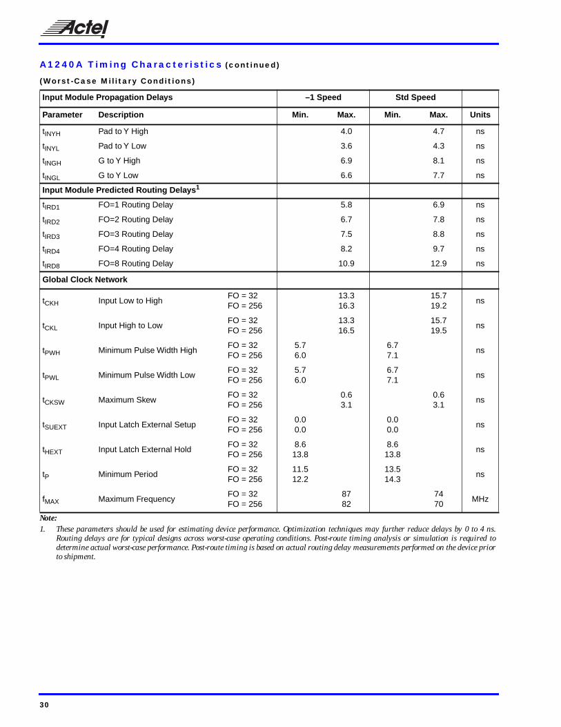
A1240A Timing Characteristics (continued)
(Worst-Case Military Conditions)
Note:1. These parameters should be used for estimating device performance. Optimization techniques may further reduce delays by 0 to 4 ns.
Routing delays are for typical designs across worst-case operating conditions. Post-route timing analysis or simulation is required todetermine actual worst-case performance. Post-route timing is based on actual routing delay measurements performed on the device priorto shipment.
Input Module Propagation Delays –1 Speed Std Speed
Parameter Description Min. Max. Min. Max. Units
tINYH Pad to Y High 4.0 4.7 ns
tINYL Pad to Y Low 3.6 4.3 ns
tINGH G to Y High 6.9 8.1 ns
tINGL G to Y Low 6.6 7.7 ns
Input Module Predicted Routing Delays 1
tIRD1 FO=1 Routing Delay 5.8 6.9 ns
tIRD2 FO=2 Routing Delay 6.7 7.8 ns
tIRD3 FO=3 Routing Delay 7.5 8.8 ns
tIRD4 FO=4 Routing Delay 8.2 9.7 ns
tIRD8 FO=8 Routing Delay 10.9 12.9 ns
Global Clock Network
tCKH Input Low to HighFO = 32FO = 256
13.316.3
15.719.2
ns
tCKL Input High to LowFO = 32FO = 256
13.316.5
15.719.5
ns
tPWH Minimum Pulse Width HighFO = 32FO = 256
5.76.0
6.77.1
ns
tPWL Minimum Pulse Width LowFO = 32FO = 256
5.76.0
6.77.1
ns
tCKSW Maximum SkewFO = 32FO = 256
0.63.1
0.63.1
ns
tSUEXT Input Latch External SetupFO = 32FO = 256
0.00.0
0.00.0
ns
tHEXT Input Latch External HoldFO = 32FO = 256
8.613.8
8.613.8
ns
tP Minimum PeriodFO = 32FO = 256
11.512.2
13.514.3
ns
fMAX Maximum FrequencyFO = 32FO = 256
8782
7470
MHz
30
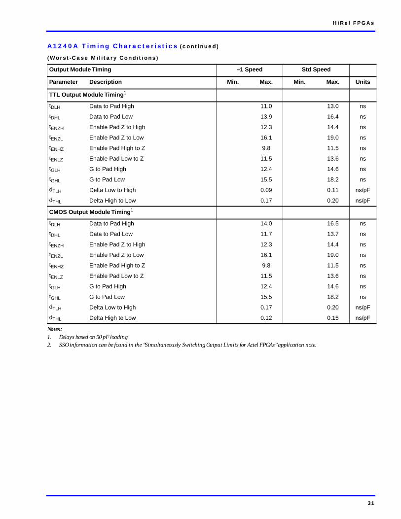
HiRel FPGAs
A1240A Timing Characteristics (continued)
(Worst-Case Military Conditions)
Notes:1. Delays based on 50 pF loading.2. SSO information can be found in the “Simultaneously Switching Output Limits for Actel FPGAs” application note.
Output Module Timing –1 Speed Std Speed
Parameter Description Min. Max. Min. Max. Units
TTL Output Module Timing 1
tDLH Data to Pad High 11.0 13.0 ns
tDHL Data to Pad Low 13.9 16.4 ns
tENZH Enable Pad Z to High 12.3 14.4 ns
tENZL Enable Pad Z to Low 16.1 19.0 ns
tENHZ Enable Pad High to Z 9.8 11.5 ns
tENLZ Enable Pad Low to Z 11.5 13.6 ns
tGLH G to Pad High 12.4 14.6 ns
tGHL G to Pad Low 15.5 18.2 ns
dTLH Delta Low to High 0.09 0.11 ns/pF
dTHL Delta High to Low 0.17 0.20 ns/pF
CMOS Output Module Timing 1
tDLH Data to Pad High 14.0 16.5 ns
tDHL Data to Pad Low 11.7 13.7 ns
tENZH Enable Pad Z to High 12.3 14.4 ns
tENZL Enable Pad Z to Low 16.1 19.0 ns
tENHZ Enable Pad High to Z 9.8 11.5 ns
tENLZ Enable Pad Low to Z 11.5 13.6 ns
tGLH G to Pad High 12.4 14.6 ns
tGHL G to Pad Low 15.5 18.2 ns
dTLH Delta Low to High 0.17 0.20 ns/pF
dTHL Delta High to Low 0.12 0.15 ns/pF
31
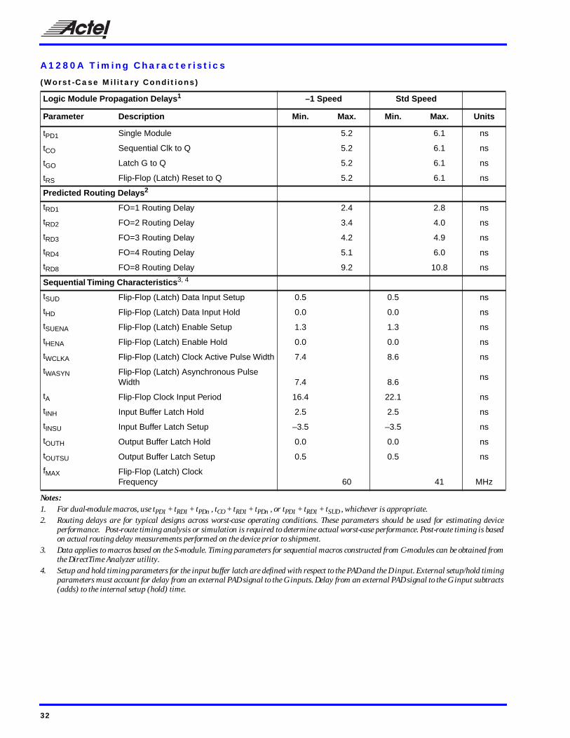
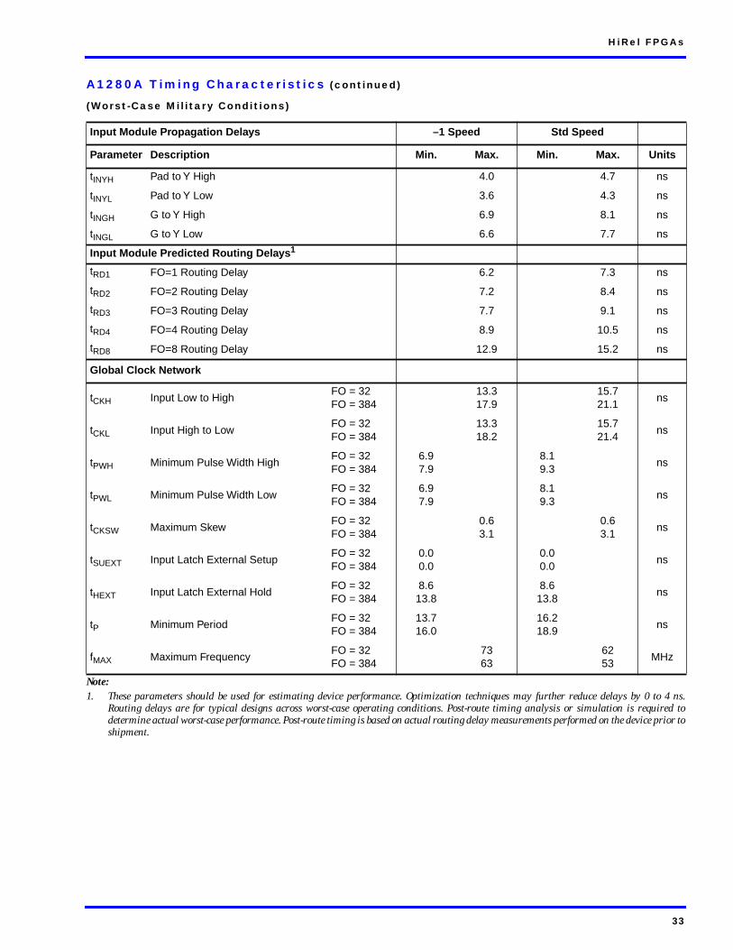
A1280A Timing Characteristics
(Worst-Case Military Conditions)
Notes:1. For dual-module macros, use tPD1 + tRD1 + tPDn , tCO + tRD1 + tPDn , or tPD1 + tRD1 + tSUD , whichever is appropriate.2. Routing delays are for typical designs across worst-case operating conditions. These parameters should be used for estimating device
performance. Post-route timing analysis or simulation is required to determine actual worst-case performance. Post-route timing is basedon actual routing delay measurements performed on the device prior to shipment.
3. Data applies to macros based on the S-module. Timing parameters for sequential macros constructed from C-modules can be obtained fromthe DirectTime Analyzer utility.
4. Setup and hold timing parameters for the input buffer latch are defined with respect to the PAD and the D input. External setup/hold timingparameters must account for delay from an external PAD signal to the G inputs. Delay from an external PAD signal to the G input subtracts(adds) to the internal setup (hold) time.
Logic Module Propagation Delays 1 –1 Speed Std Speed
Parameter Description Min. Max. Min. Max. Units
tPD1 Single Module 5.2 6.1 ns
tCO Sequential Clk to Q 5.2 6.1 ns
tGO Latch G to Q 5.2 6.1 ns
tRS Flip-Flop (Latch) Reset to Q 5.2 6.1 ns
Predicted Routing Delays 2
tRD1 FO=1 Routing Delay 2.4 2.8 ns
tRD2 FO=2 Routing Delay 3.4 4.0 ns
tRD3 FO=3 Routing Delay 4.2 4.9 ns
tRD4 FO=4 Routing Delay 5.1 6.0 ns
tRD8 FO=8 Routing Delay 9.2 10.8 ns
Sequential Timing Characteristics 3, 4
tSUD Flip-Flop (Latch) Data Input Setup 0.5 0.5 ns
tHD Flip-Flop (Latch) Data Input Hold 0.0 0.0 ns
tSUENA Flip-Flop (Latch) Enable Setup 1.3 1.3 ns
tHENA Flip-Flop (Latch) Enable Hold 0.0 0.0 ns
tWCLKA Flip-Flop (Latch) Clock Active Pulse Width 7.4 8.6 ns
tWASYN Flip-Flop (Latch) Asynchronous Pulse Width 7.4 8.6
ns
tA Flip-Flop Clock Input Period 16.4 22.1 ns
tINH Input Buffer Latch Hold 2.5 2.5 ns
tINSU Input Buffer Latch Setup –3.5 –3.5 ns
tOUTH Output Buffer Latch Hold 0.0 0.0 ns
tOUTSU Output Buffer Latch Setup 0.5 0.5 ns
fMAX Flip-Flop (Latch) Clock Frequency 60 41 MHz
32
HiRel FPGAs
A1280A Timing Characteristics (continued)
(Worst-Case Military Conditions)
Note:1. These parameters should be used for estimating device performance. Optimization techniques may further reduce delays by 0 to 4 ns.
Routing delays are for typical designs across worst-case operating conditions. Post-route timing analysis or simulation is required todetermine actual worst-case performance. Post-route timing is based on actual routing delay measurements performed on the device prior toshipment.
Input Module Propagation Delays –1 Speed Std Speed
Parameter Description Min. Max. Min. Max. Units
tINYH Pad to Y High 4.0 4.7 ns
tINYL Pad to Y Low 3.6 4.3 ns
tINGH G to Y High 6.9 8.1 ns
tINGL G to Y Low 6.6 7.7 ns
Input Module Predicted Routing Delays 1
tRD1 FO=1 Routing Delay 6.2 7.3 ns
tRD2 FO=2 Routing Delay 7.2 8.4 ns
tRD3 FO=3 Routing Delay 7.7 9.1 ns
tRD4 FO=4 Routing Delay 8.9 10.5 ns
tRD8 FO=8 Routing Delay 12.9 15.2 ns
Global Clock Network
tCKH Input Low to HighFO = 32FO = 384
13.317.9
15.721.1
ns
tCKL Input High to LowFO = 32FO = 384
13.318.2
15.721.4
ns
tPWH Minimum Pulse Width HighFO = 32FO = 384
6.97.9
8.19.3
ns
tPWL Minimum Pulse Width LowFO = 32FO = 384
6.97.9
8.19.3
ns
tCKSW Maximum SkewFO = 32FO = 384
0.63.1
0.63.1
ns
tSUEXT Input Latch External SetupFO = 32FO = 384
0.00.0
0.00.0
ns
tHEXT Input Latch External HoldFO = 32FO = 384
8.613.8
8.613.8
ns
tP Minimum PeriodFO = 32FO = 384
13.716.0
16.218.9
ns
fMAX Maximum FrequencyFO = 32FO = 384
7363
6253
MHz
33

A1280A Timing Characteristics (continued)
(Worst-Case Military Conditions)
Notes:1. Delays based on 50 pF loading.2. SSO information can be found in the “Simultaneously Switching Output Limits for Actel FPGAs” application note.
Output Module Timing –1 Speed Std Speed
Parameter Description Min. Max. Min. Max. Units
TTL Output Module Timing 1
tDLH Data to Pad High 11.0 13.0 ns
tDHL Data to Pad Low 13.9 16.4 ns
tENZH Enable Pad Z to High 12.3 14.4 ns
tENZL Enable Pad Z to Low 16.1 19.0 ns
tENHZ Enable Pad High to Z 9.8 11.5 ns
tENLZ Enable Pad Low to Z 11.5 13.6 ns
tGLH G to Pad High 12.4 14.6 ns
tGHL G to Pad Low 15.5 18.2 ns
dTLH Delta Low to High 0.09 0.11 ns/pF
dTHL Delta High to Low 0.17 0.20 ns/pF
CMOS Output Module Timing 1
tDLH Data to Pad High 14.0 16.5 ns
tDHL Data to Pad Low 11.7 13.7 ns
tENZH Enable Pad Z to High 12.3 14.4 ns
tENZL Enable Pad Z to Low 16.1 19.0 ns
tENHZ Enable Pad High to Z 9.8 11.5 ns
tENLZ Enable Pad Low to Z 11.5 13.6 ns
tGLH G to Pad High 12.4 14.6 ns
tGHL G to Pad Low 15.5 18.2 ns
dTLH Delta Low to High 0.17 0.20 ns/pF
dTHL Delta High to Low 0.12 0.15 ns/pF
34
HiRel FPGAs
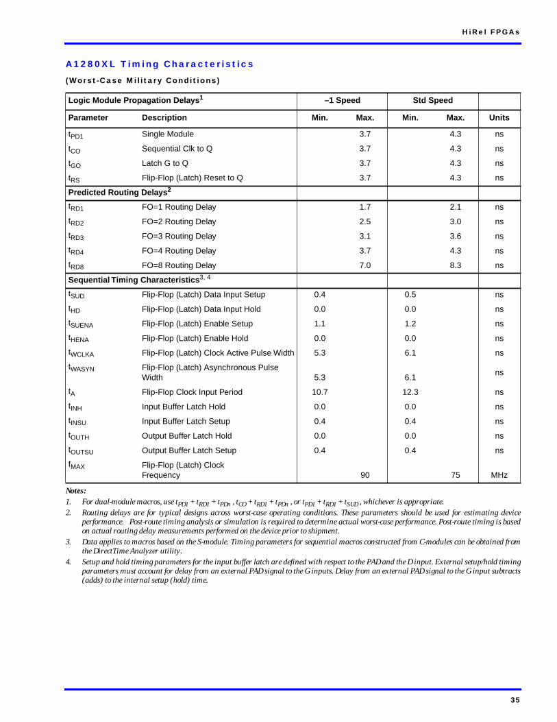
A1280XL Timing Characteristics
(Worst-Case Military Conditions)
Notes:1. For dual-module macros, use tPD1 + tRD1 + tPDn , tCO + tRD1 + tPDn , or tPD1 + tRD1 + tSUD , whichever is appropriate.2. Routing delays are for typical designs across worst-case operating conditions. These parameters should be used for estimating device
performance. Post-route timing analysis or simulation is required to determine actual worst-case performance. Post-route timing is basedon actual routing delay measurements performed on the device prior to shipment.
3. Data applies to macros based on the S-module. Timing parameters for sequential macros constructed from C-modules can be obtained fromthe DirectTime Analyzer utility.
4. Setup and hold timing parameters for the input buffer latch are defined with respect to the PAD and the D input. External setup/hold timingparameters must account for delay from an external PAD signal to the G inputs. Delay from an external PAD signal to the G input subtracts(adds) to the internal setup (hold) time.
Logic Module Propagation Delays 1 –1 Speed Std Speed
Parameter Description Min. Max. Min. Max. Units
tPD1 Single Module 3.7 4.3 ns
tCO Sequential Clk to Q 3.7 4.3 ns
tGO Latch G to Q 3.7 4.3 ns
tRS Flip-Flop (Latch) Reset to Q 3.7 4.3 ns
Predicted Routing Delays 2
tRD1 FO=1 Routing Delay 1.7 2.1 ns
tRD2 FO=2 Routing Delay 2.5 3.0 ns
tRD3 FO=3 Routing Delay 3.1 3.6 ns
tRD4 FO=4 Routing Delay 3.7 4.3 ns
tRD8 FO=8 Routing Delay 7.0 8.3 ns
Sequential Timing Characteristics 3, 4
tSUD Flip-Flop (Latch) Data Input Setup 0.4 0.5 ns
tHD Flip-Flop (Latch) Data Input Hold 0.0 0.0 ns
tSUENA Flip-Flop (Latch) Enable Setup 1.1 1.2 ns
tHENA Flip-Flop (Latch) Enable Hold 0.0 0.0 ns
tWCLKA Flip-Flop (Latch) Clock Active Pulse Width 5.3 6.1 ns
tWASYN Flip-Flop (Latch) Asynchronous Pulse Width 5.3 6.1
ns
tA Flip-Flop Clock Input Period 10.7 12.3 ns
tINH Input Buffer Latch Hold 0.0 0.0 ns
tINSU Input Buffer Latch Setup 0.4 0.4 ns
tOUTH Output Buffer Latch Hold 0.0 0.0 ns
tOUTSU Output Buffer Latch Setup 0.4 0.4 ns
fMAX Flip-Flop (Latch) Clock Frequency 90 75 MHz
35
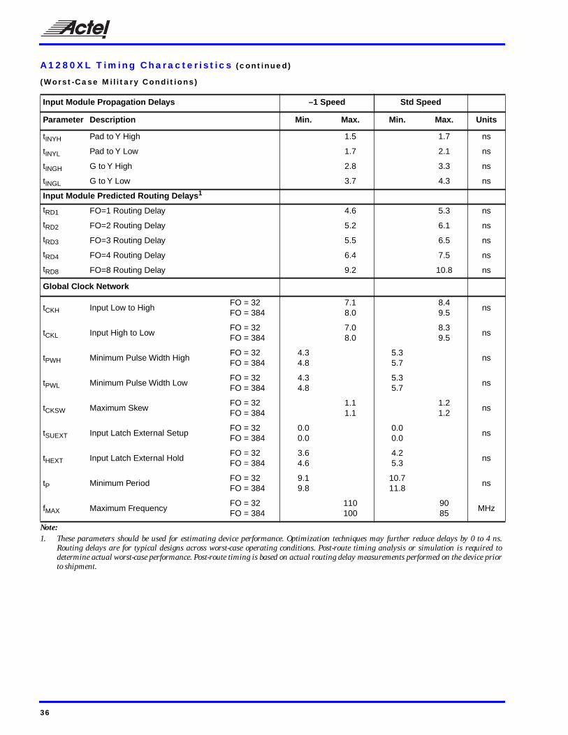
A1280XL Timing Characteristics (continued)
(Worst-Case Military Conditions)
Note:1. These parameters should be used for estimating device performance. Optimization techniques may further reduce delays by 0 to 4 ns.
Routing delays are for typical designs across worst-case operating conditions. Post-route timing analysis or simulation is required todetermine actual worst-case performance. Post-route timing is based on actual routing delay measurements performed on the device priorto shipment.
Input Module Propagation Delays –1 Speed Std Speed
Parameter Description Min. Max. Min. Max. Units
tINYH Pad to Y High 1.5 1.7 ns
tINYL Pad to Y Low 1.7 2.1 ns
tINGH G to Y High 2.8 3.3 ns
tINGL G to Y Low 3.7 4.3 ns
Input Module Predicted Routing Delays 1
tRD1 FO=1 Routing Delay 4.6 5.3 ns
tRD2 FO=2 Routing Delay 5.2 6.1 ns
tRD3 FO=3 Routing Delay 5.5 6.5 ns
tRD4 FO=4 Routing Delay 6.4 7.5 ns
tRD8 FO=8 Routing Delay 9.2 10.8 ns
Global Clock Network
tCKH Input Low to HighFO = 32FO = 384
7.18.0
8.49.5
ns
tCKL Input High to LowFO = 32FO = 384
7.08.0
8.39.5
ns
tPWH Minimum Pulse Width HighFO = 32FO = 384
4.34.8
5.35.7
ns
tPWL Minimum Pulse Width LowFO = 32FO = 384
4.34.8
5.35.7
ns
tCKSW Maximum SkewFO = 32FO = 384
1.11.1
1.21.2
ns
tSUEXT Input Latch External SetupFO = 32FO = 384
0.00.0
0.00.0
ns
tHEXT Input Latch External HoldFO = 32FO = 384
3.64.6
4.25.3
ns
tP Minimum PeriodFO = 32FO = 384
9.19.8
10.711.8
ns
fMAX Maximum FrequencyFO = 32FO = 384
110100
9085
MHz
36

HiRel FPGAs
A1280XL Timing Characteristics (continued)
(Worst-Case Military Conditions)
Notes:1. Delays based on 50 pF loading.2. SSO information can be found in the “Simultaneously Switching Output Limits for Actel FPGAs” application note.
Output Module Timing –1 Speed Std Speed
Parameter Description Min. Max. Min. Max. Units
TTL Output Module Timing 1
tDLH Data to Pad High 5.3 6.2 ns
tDHL Data to Pad Low 5.7 6.6 ns
tENZH Enable Pad Z to High 5.3 6.2 ns
tENZL Enable Pad Z to Low 5.8 6.8 ns
tENHZ Enable Pad High to Z 7.5 8.9 ns
tENLZ Enable Pad Low to Z 7.5 8.9 ns
tGLH G to Pad High 5.9 6.9 ns
tGHL G to Pad Low 6.6 7.8 ns
dTLH Delta Low to High 0.05 0.06 ns/pF
dTHL Delta High to Low 0.05 0.09 ns/pF
CMOS Output Module Timing 1
tDLH Data to Pad High 6.6 7.9 ns
tDHL Data to Pad Low 4.7 5.5 ns
tENZH Enable Pad Z to High 5.3 6.2 ns
tENZL Enable Pad Z to Low 5.8 6.8 ns
tENHZ Enable Pad High to Z 7.5 8.9 ns
tENLZ Enable Pad Low to Z 7.5 8.9 ns
tGLH G to Pad High 5.9 6.9 ns
tGHL G to Pad Low 6.6 7.8 ns
dTLH Delta Low to High 0.07 0.09 ns/pF
dTHL Delta High to Low 0.06 0.09 ns/pF
37

A1425A Timing Characteristics
(Worst-Case Military Conditions)
Notes:1. For dual-module macros, use tPD + tRD1 + tPDn , tCO + tRD1 + tPDn , or tPD1 + tRD1 + tSUD , whichever is appropriate.2. Routing delays are for typical designs across worst-case operating conditions. These parameters should be used for estimating device
performance. Post-route timing analysis or simulation is required to determine actual worst-case performance. Post-route timing is basedon actual routing delay measurements performed on the device prior to shipment.
Logic Module Propagation Delays 1 –1 Speed Std Speed
Parameter Description Min. Max. Min. Max. Units
tPD Internal Array Module 3.0 3.5 ns
tCO Sequential Clock to Q 3.0 3.5 ns
tCLR Asynchronous Clear to Q 3.0 3.5 ns
Predicted Routing Delays 2
tRD1 FO=1 Routing Delay 1.3 1.5 ns
tRD2 FO=2 Routing Delay 1.9 2.1 ns
tRD3 FO=3 Routing Delay 2.1 2.5 ns
tRD4 FO=4 Routing Delay 2.6 2.9 ns
tRD8 FO=8 Routing Delay 4.2 4.9 ns
Logic Module Sequential Timing
tSUD Flip-Flop (Latch) Data Input Setup 0.9 1.0 ns
tHD Flip-Flop (Latch) Data Input Hold 0.0 0.0 ns
tSUENA Flip-Flop (Latch) Enable Setup 0.9 1.0 ns
tHENA Flip-Flop (Latch) Enable Hold 0.0 0.0 ns
tWASYN Asynchronous Pulse Width 3.8 4.4 ns
tWCLKA Flip-Flop Clock Pulse Width 3.8 4.4 ns
tA Flip-Flop Clock Input Period 7.9 9.3 ns
fMAX Flip-Flop Clock Frequency 125 100 MHz
38
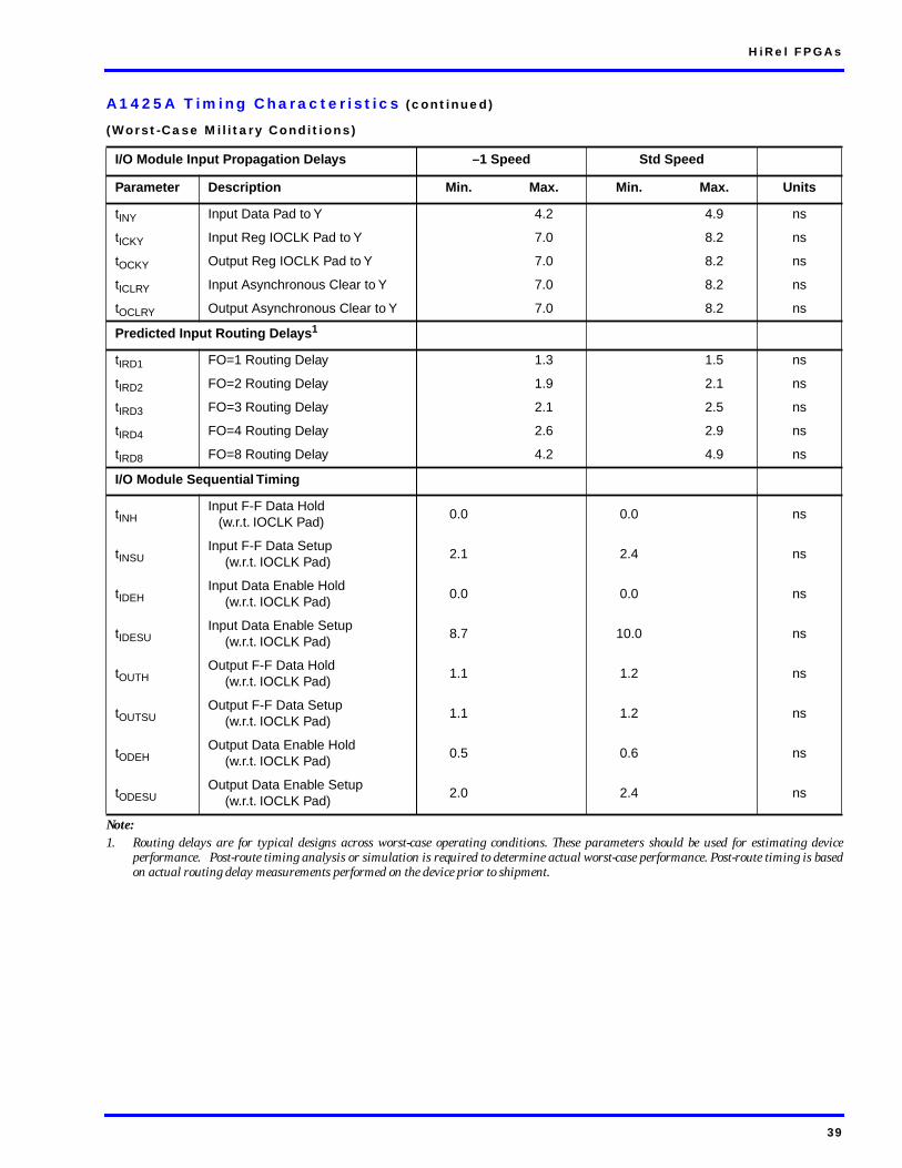
HiRel FPGAs
A1425A Timing Characteristics (continued)
(Worst-Case Military Conditions)
Note:1. Routing delays are for typical designs across worst-case operating conditions. These parameters should be used for estimating device
performance. Post-route timing analysis or simulation is required to determine actual worst-case performance. Post-route timing is basedon actual routing delay measurements performed on the device prior to shipment.
I/O Module Input Propagation Delays –1 Speed Std Speed
Parameter Description Min. Max. Min. Max. Units
tINY Input Data Pad to Y 4.2 4.9 ns
tICKY Input Reg IOCLK Pad to Y 7.0 8.2 ns
tOCKY Output Reg IOCLK Pad to Y 7.0 8.2 ns
tICLRY Input Asynchronous Clear to Y 7.0 8.2 ns
tOCLRY Output Asynchronous Clear to Y 7.0 8.2 ns
Predicted Input Routing Delays 1
tIRD1 FO=1 Routing Delay 1.3 1.5 ns
tIRD2 FO=2 Routing Delay 1.9 2.1 ns
tIRD3 FO=3 Routing Delay 2.1 2.5 ns
tIRD4 FO=4 Routing Delay 2.6 2.9 ns
tIRD8 FO=8 Routing Delay 4.2 4.9 ns
I/O Module Sequential Timing
tINHInput F-F Data Hold (w.r.t. IOCLK Pad)
0.0 0.0 ns
tINSUInput F-F Data Setup
(w.r.t. IOCLK Pad)2.1 2.4 ns
tIDEHInput Data Enable Hold
(w.r.t. IOCLK Pad) 0.0 0.0 ns
tIDESUInput Data Enable Setup
(w.r.t. IOCLK Pad) 8.7 10.0 ns
tOUTHOutput F-F Data Hold
(w.r.t. IOCLK Pad) 1.1 1.2 ns
tOUTSUOutput F-F Data Setup
(w.r.t. IOCLK Pad) 1.1 1.2 ns
tODEHOutput Data Enable Hold
(w.r.t. IOCLK Pad)0.5 0.6 ns
tODESUOutput Data Enable Setup
(w.r.t. IOCLK Pad) 2.0 2.4 ns
39

A1425A Timing Characteristics (continued)
(Worst-Case Military Conditions)
Notes:1. Delays based on 35 pF loading.2. SSO information can be found in the “Simultaneously Switching Output Limits for Actel FPGAs” application note.
I/O Module – TTL Output Timing 1 –1 Speed Std Speed
Parameter Description Min. Max. Min. Max. Units
tDHS Data to Pad, High Slew 7.5 8.9 ns
tDLS Data to Pad, Low Slew 11.9 14.0 ns
tENZHS Enable to Pad, Z to H/L, Hi Slew 6.0 7.0 ns
tENZLS Enable to Pad, Z to H/L, Lo Slew 10.9 12.8 ns
tENHSZ Enable to Pad, H/L to Z, Hi Slew 9.9 11.6 ns
tENLSZ Enable to Pad, H/L to Z, Lo Slew 9.9 11.6 ns
tCKHS IOCLK Pad to Pad H/L, Hi Slew 10.5 11.6 ns
tCKLS IOCLK Pad to Pad H/L, Lo Slew 15.7 17.4 ns
dTLHHS Delta Low to High, Hi Slew 0.04 0.04 ns/pF
dTLHLS Delta Low to High, Lo Slew 0.07 0.08 ns/pF
dTHLHS Delta High to Low, Hi Slew 0.05 0.06 ns/pF
dTHLLS Delta High to Low, Lo Slew 0.07 0.08 ns/pF
I/O Module – CMOS Output Timing 1
tDHS Data to Pad, High Slew 9.2 10.8 ns
tDLS Data to Pad, Low Slew 17.3 20.3 ns
tENZHS Enable to Pad, Z to H/L, Hi Slew 7.7 9.1 ns
tENZLS Enable to Pad, Z to H/L, Lo Slew 13.1 15.5 ns
tENHSZ Enable to Pad, H/L to Z, Hi Slew 9.9 11.6 ns
tENLSZ Enable to Pad, H/L to Z, Lo Slew 10.5 11.6 ns
tCKHS IOCLK Pad to Pad H/L, Hi Slew 12.5 13.7 ns
tCKLS IOCLK Pad to Pad H/L, Lo Slew 18.1 20.1 ns
dTLHHS Delta Low to High, Hi Slew 0.06 0.07 ns/pF
dTLHLS Delta Low to High, Lo Slew 0.11 0.13 ns/pF
dTHLHS Delta High to Low, Hi Slew 0.04 0.05 ns/pF
dTHLLS Delta High to Low, Lo Slew 0.05 0.06 ns/pF
40
HiRel FPGAs
A1425A Timing Characteristics (continued)
(Worst-Case Military Conditions)
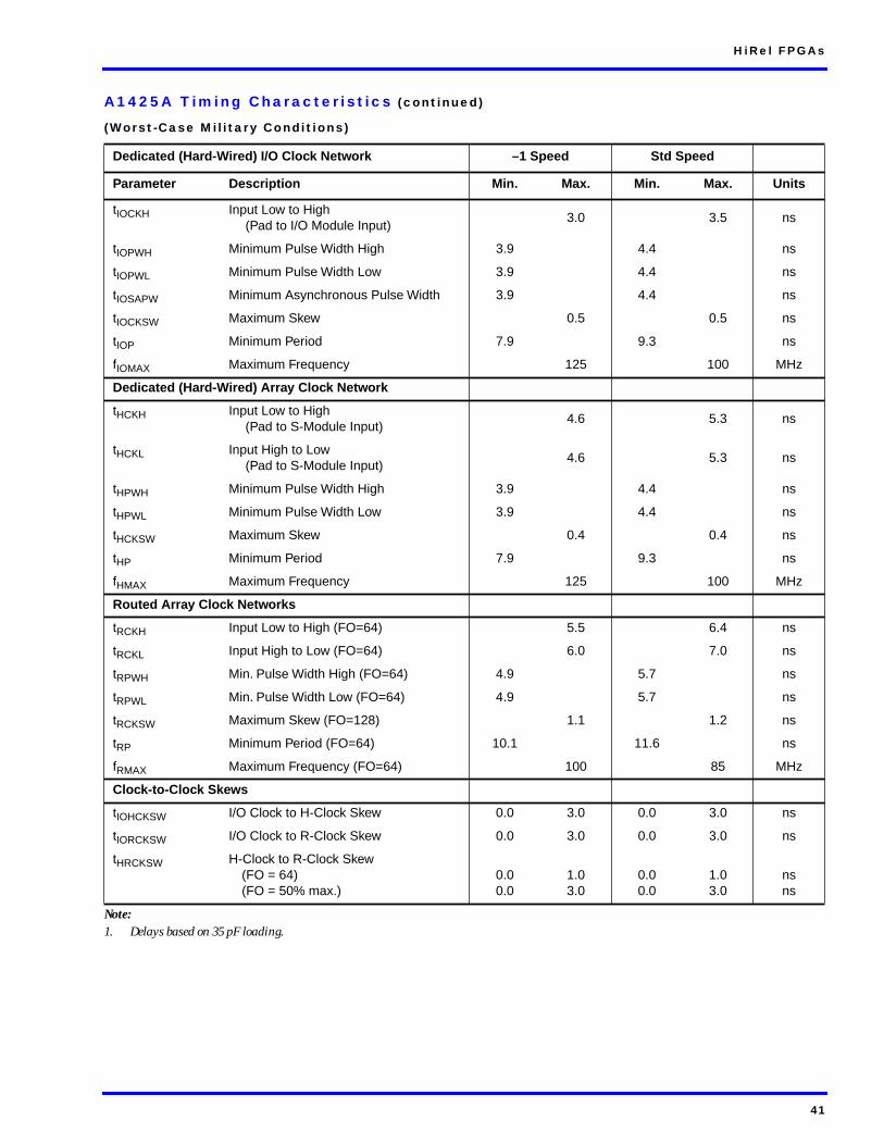
Note:1. Delays based on 35 pF loading.
Dedicated (Hard-Wired) I/O Clock Network –1 Speed Std Speed
Parameter Description Min. Max. Min. Max. Units
tIOCKH Input Low to High (Pad to I/O Module Input)
3.0 3.5 ns
tIOPWH Minimum Pulse Width High 3.9 4.4 ns
tIOPWL Minimum Pulse Width Low 3.9 4.4 ns
tIOSAPW Minimum Asynchronous Pulse Width 3.9 4.4 ns
tIOCKSW Maximum Skew 0.5 0.5 ns
tIOP Minimum Period 7.9 9.3 ns
fIOMAX Maximum Frequency 125 100 MHz
Dedicated (Hard-Wired) Array Clock Network
tHCKH Input Low to High (Pad to S-Module Input)
4.6 5.3 ns
tHCKL Input High to Low (Pad to S-Module Input)
4.6 5.3 ns
tHPWH Minimum Pulse Width High 3.9 4.4 ns
tHPWL Minimum Pulse Width Low 3.9 4.4 ns
tHCKSW Maximum Skew 0.4 0.4 ns
tHP Minimum Period 7.9 9.3 ns
fHMAX Maximum Frequency 125 100 MHz
Routed Array Clock Networks
tRCKH Input Low to High (FO=64) 5.5 6.4 ns
tRCKL Input High to Low (FO=64) 6.0 7.0 ns
tRPWH Min. Pulse Width High (FO=64) 4.9 5.7 ns
tRPWL Min. Pulse Width Low (FO=64) 4.9 5.7 ns
tRCKSW Maximum Skew (FO=128) 1.1 1.2 ns
tRP Minimum Period (FO=64) 10.1 11.6 ns
fRMAX Maximum Frequency (FO=64) 100 85 MHz
Clock-to-Clock Skews
tIOHCKSW I/O Clock to H-Clock Skew 0.0 3.0 0.0 3.0 ns
tIORCKSW I/O Clock to R-Clock Skew 0.0 3.0 0.0 3.0 ns
tHRCKSW H-Clock to R-Clock Skew(FO = 64)(FO = 50% max.)
0.00.0
1.03.0
0.00.0
1.03.0
nsns
41
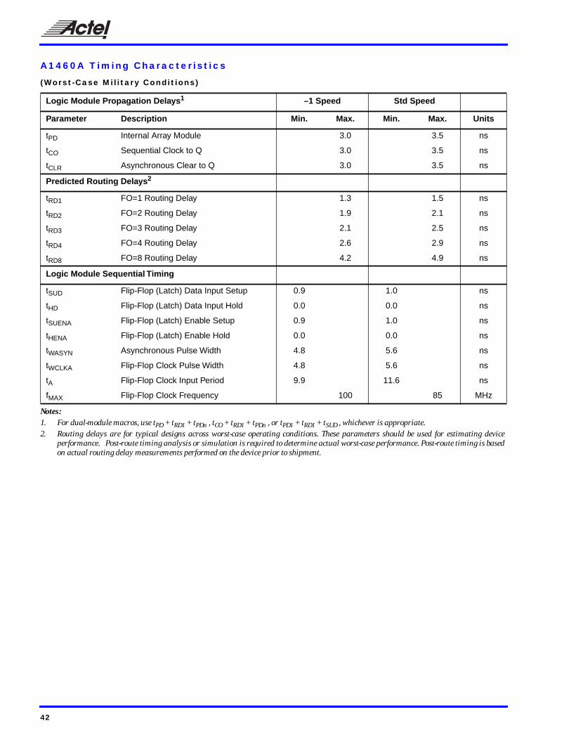
A1460A Timing Characteristics
(Worst-Case Military Conditions)
Notes:1. For dual-module macros, use tPD + tRD1 + tPDn , tCO + tRD1 + tPDn , or tPD1 + tRD1 + tSUD , whichever is appropriate.2. Routing delays are for typical designs across worst-case operating conditions. These parameters should be used for estimating device
performance. Post-route timing analysis or simulation is required to determine actual worst-case performance. Post-route timing is basedon actual routing delay measurements performed on the device prior to shipment.
Logic Module Propagation Delays 1 –1 Speed Std Speed
Parameter Description Min. Max. Min. Max. Units
tPD Internal Array Module 3.0 3.5 ns
tCO Sequential Clock to Q 3.0 3.5 ns
tCLR Asynchronous Clear to Q 3.0 3.5 ns
Predicted Routing Delays 2
tRD1 FO=1 Routing Delay 1.3 1.5 ns
tRD2 FO=2 Routing Delay 1.9 2.1 ns
tRD3 FO=3 Routing Delay 2.1 2.5 ns
tRD4 FO=4 Routing Delay 2.6 2.9 ns
tRD8 FO=8 Routing Delay 4.2 4.9 ns
Logic Module Sequential Timing
tSUD Flip-Flop (Latch) Data Input Setup 0.9 1.0 ns
tHD Flip-Flop (Latch) Data Input Hold 0.0 0.0 ns
tSUENA Flip-Flop (Latch) Enable Setup 0.9 1.0 ns
tHENA Flip-Flop (Latch) Enable Hold 0.0 0.0 ns
tWASYN Asynchronous Pulse Width 4.8 5.6 ns
tWCLKA Flip-Flop Clock Pulse Width 4.8 5.6 ns
tA Flip-Flop Clock Input Period 9.9 11.6 ns
fMAX Flip-Flop Clock Frequency 100 85 MHz
42
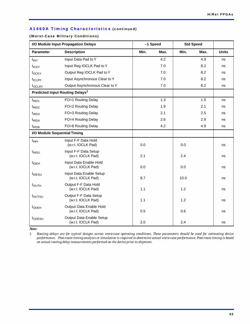
HiRel FPGAs
A1460A Timing Characteristics (continued)
(Worst-Case Military Conditions)
Note:1. Routing delays are for typical designs across worst-case operating conditions. These parameters should be used for estimating device
performance. Post-route timing analysis or simulation is required to determine actual worst-case performance. Post-route timing is basedon actual routing delay measurements performed on the device prior to shipment.
I/O Module Input Propagation Delays –1 Speed Std Speed
Parameter Description Min. Max. Min. Max. Units
tINY Input Data Pad to Y 4.2 4.9 ns
tICKY Input Reg IOCLK Pad to Y 7.0 8.2 ns
tOCKY Output Reg IOCLK Pad to Y 7.0 8.2 ns
tICLRY Input Asynchronous Clear to Y 7.0 8.2 ns
tOCLRY Output Asynchronous Clear to Y 7.0 8.2 ns
Predicted Input Routing Delays 1
tIRD1 FO=1 Routing Delay 1.3 1.5 ns
tIRD2 FO=2 Routing Delay 1.9 2.1 ns
tIRD3 FO=3 Routing Delay 2.1 2.5 ns
tIRD4 FO=4 Routing Delay 2.6 2.9 ns
tIRD8 FO=8 Routing Delay 4.2 4.9 ns
I/O Module Sequential Timing
tINH Input F-F Data Hold (w.r.t. IOCLK Pad) 0.0 0.0 ns
tINSU Input F-F Data Setup (w.r.t. IOCLK Pad) 2.1 2.4 ns
tIDEH Input Data Enable Hold (w.r.t. IOCLK Pad) 0.0 0.0 ns
tIDESU Input Data Enable Setup (w.r.t. IOCLK Pad) 8.7 10.0 ns
tOUTH Output F-F Data Hold (w.r.t. IOCLK Pad) 1.1 1.2 ns
tOUTSU Output F-F Data Setup (w.r.t. IOCLK Pad) 1.1 1.2 ns
tODEH Output Data Enable Hold (w.r.t. IOCLK Pad) 0.5 0.6 ns
tODESU Output Data Enable Setup (w.r.t. IOCLK Pad) 2.0 2.4 ns
43

A1460A Timing Characteristics (continued)
(Worst-Case Military Conditions)
Notes:1. Delays based on 35 pF loading.2. SSO information can be found in the “Simultaneously Switching Output Limits for Actel FPGAs” application note.
I/O Module – TTL Output Timing 1 –1 Speed Std Speed
Parameter Description Min. Max. Min. Max. Units
tDHS Data to Pad, High Slew 7.5 8.9 ns
tDLS Data to Pad, Low Slew 11.9 14.0 ns
tENZHS Enable to Pad, Z to H/L, Hi Slew 6.0 7.0 ns
tENZLS Enable to Pad, Z to H/L, Lo Slew 10.9 12.8 ns
tENHSZ Enable to Pad, H/L to Z, Hi Slew 11.5 13.5 ns
tENLSZ Enable to Pad, H/L to Z, Lo Slew 10.9 12.8 ns
tCKHS IOCLK Pad to Pad H/L, Hi Slew 11.6 13.4 ns
tCKLS IOCLK Pad to Pad H/L, Lo Slew 17.8 19.8 ns
dTLHHS Delta Low to High, Hi Slew 0.04 0.04 ns/pF
dTLHLS Delta Low to High, Lo Slew 0.07 0.08 ns/pF
dTHLHS Delta High to Low, Hi Slew 0.05 0.06 ns/pF
dTHLLS Delta High to Low, Lo Slew 0.07 0.08 ns/pF
I/O Module – CMOS Output Timing 1
tDHS Data to Pad, High Slew 9.2 10.8 ns
tDLS Data to Pad, Low Slew 17.3 20.3 ns
tENZHS Enable to Pad, Z to H/L, Hi Slew 7.7 9.1 ns
tENZLS Enable to Pad, Z to H/L, Lo Slew 13.1 15.5 ns
tENHSZ Enable to Pad, H/L to Z, Hi Slew 10.9 12.8 ns
tENLSZ Enable to Pad, H/L to Z, Lo Slew 10.9 12.8 ns
tCKHS IOCLK Pad to Pad H/L, Hi Slew 14.1 16.0 ns
tCKLS IOCLK Pad to Pad H/L, Lo Slew 20.2 22.4 ns
dTLHHS Delta Low to High, Hi Slew 0.06 0.07 ns/pF
dTLHLS Delta Low to High, Lo Slew 0.11 0.13 ns/pF
dTHLHS Delta High to Low, Hi Slew 0.04 0.05 ns/pF
dTHLLS Delta High to Low, Lo Slew 0.05 0.06 ns/pF
44

HiRel FPGAs
A1460A Timing Characteristics (continued)
(Worst-Case Military Conditions)
Note:1. Delays based on 35 pF loading.
Dedicated (Hard-Wired) I/O Clock Network –1 Speed Std Speed
Parameter Description Min. Max. Min. Max. Units
tIOCKH Input Low to High (Pad to I/O Module Input) 3.5 4.1 ns
tIOPWH Minimum Pulse Width High 4.8 5.7 ns
tIOPWL Minimum Pulse Width Low 4.8 5.7 ns
tIOSAPW Minimum Asynchronous Pulse Width 3.9 4.4 ns
tIOCKSW Maximum Skew 0.9 1.0 ns
tIOP Minimum Period 9.9 11.6 ns
fIOMAX Maximum Frequency 100 85 MHz
Dedicated (Hard-Wired) Array Clock Network
tHCKH Input Low to High (Pad to S-Module Input) 5.5 6.4 ns
tHCKL Input High to Low (Pad to S-Module Input) 5.5 6.4 ns
tHPWH Minimum Pulse Width High 4.8 5.7 ns
tHPWL Minimum Pulse Width Low 4.8 5.7 ns
tHCKSW Maximum Skew 0.9 1.0 ns
tHP Minimum Period 9.9 11.6 ns
fHMAX Maximum Frequency 100 85 MHz
Routed Array Clock Networks
tRCKH Input Low to High (FO=256) 9.0 10.5 ns
tRCKL Input High to Low (FO=256) 9.0 10.5 ns
tRPWH Min. Pulse Width High (FO=256) 6.3 7.1 ns
tRPWL Min. Pulse Width Low (FO=256) 6.3 7.1 ns
tRCKSW Maximum Skew (FO=128) 1.9 2.1 ns
tRP Minimum Period (FO=256) 12.9 14.5 ns
fRMAX Maximum Frequency (FO=256) 75 65 MHz
Clock-to-Clock Skews
tIOHCKSW I/O Clock to H-Clock Skew 0.0 3.0 0.0 3.0 ns
tIORCKSW I/O Clock to R-Clock Skew 0.0 5.0 0.0 5.0 ns
tHRCKSW H-Clock to R-Clock Skew(FO = 64)(FO = 50% max.)
0.00.0
1.03.0
0.00.0
1.03.0
nsns
45

A14100A Timing Characteristics
(Worst-Case Military Conditions)
Notes:1. For dual-module macros, use tPD + tRD1 + tPDn , tCO + tRD1 + tPDn , or tPD1 + tRD1 + tSUD , whichever is appropriate.2. Routing delays are for typical designs across worst-case operating conditions. These parameters should be used for estimating device
performance. Post-route timing analysis or simulation is required to determine actual worst-case performance. Post-route timing is basedon actual routing delay measurements performed on the device prior to shipment.
Logic Module Propagation Delays 1 –1 Speed Std Speed
Parameter Description Min. Max. Min. Max. Units
tPD Internal Array Module 3.0 3.5 ns
tCO Sequential Clock to Q 3.0 3.5 ns
tCLR Asynchronous Clear to Q 3.0 3.5 ns
Predicted Routing Delays 2
tRD1 FO=1 Routing Delay 1.3 1.5 ns
tRD2 FO=2 Routing Delay 1.9 2.1 ns
tRD3 FO=3 Routing Delay 2.1 2.5 ns
tRD4 FO=4 Routing Delay 2.6 2.9 ns
tRD8 FO=8 Routing Delay 4.2 4.9 ns
Logic Module Sequential Timing
tSUD Flip-Flop (Latch) Data Input Setup 1.0 1.0 ns
tHD Flip-Flop (Latch) Data Input Hold 0.6 0.6 ns
tSUENA Flip-Flop (Latch) Enable Setup 1.0 1.0 ns
tHENA Flip-Flop (Latch) Enable Hold 0.6 0.6 ns
tWASYN Asynchronous Pulse Width 4.8 5.6 ns
tWCLKA Flip-Flop Clock Pulse Width 4.8 5.6 ns
tA Flip-Flop Clock Input Period 9.9 11.6 ns
fMAX Flip-Flop Clock Frequency 100 85 MHz
46

HiRel FPGAs
A14100A Timing Characteristics (continued)
(Worst-Case Military Conditions )
Note:1. Routing delays are for typical designs across worst-case operating conditions. These parameters should be used for estimating device
performance. Post-route timing analysis or simulation is required to determine actual worst-case performance. Post-route timing is basedon actual routing delay measurements performed on the device prior to shipment.
I/O Module Input Propagation Delays –1 Speed Std Speed
Parameter Description Min. Max. Min. Max. Units
tINY Input Data Pad to Y 4.2 4.9 ns
tICKY Input Reg IOCLK Pad to Y 7.0 8.2 ns
tOCKY Output Reg IOCLK Pad to Y 7.0 8.2 ns
tICLRY Input Asynchronous Clear to Y 7.0 8.2 ns
tOCLRY Output Asynchronous Clear to Y 7.0 8.2 ns
Predicted Input Routing Delays 1
tIRD1 FO=1 Routing Delay 1.3 1.5 ns
tIRD2 FO=2 Routing Delay 1.9 2.1 ns
tIRD3 FO=3 Routing Delay 2.1 2.5 ns
tIRD4 FO=4 Routing Delay 2.6 2.9 ns
tIRD8 FO=8 Routing Delay 4.2 4.9 ns
I/O Module Sequential Timing
tINH Input F-F Data Hold (w.r.t. IOCLK Pad) 0.0 0.0 ns
tINSU Input F-F Data Setup (w.r.t. IOCLK Pad) 2.1 2.4 ns
tIDEH Input Data Enable Hold (w.r.t. IOCLK Pad) 0.0 0.0 ns
tIDESU Input Data Enable Setup (w.r.t. IOCLK Pad) 8.7 10.0 ns
tOUTH Output F-F Data Hold (w.r.t. IOCLK Pad) 1.2 1.2 ns
tOUTSU Output F-F Data Setup (w.r.t. IOCLK Pad) 1.2 1.2 ns
tODEH Output Data Enable Hold (w.r.t. IOCLK Pad) 0.6 0.6 ns
tODESU Output Data Enable Setup (w.r.t. IOCLK Pad) 2.4 2.4 ns
47
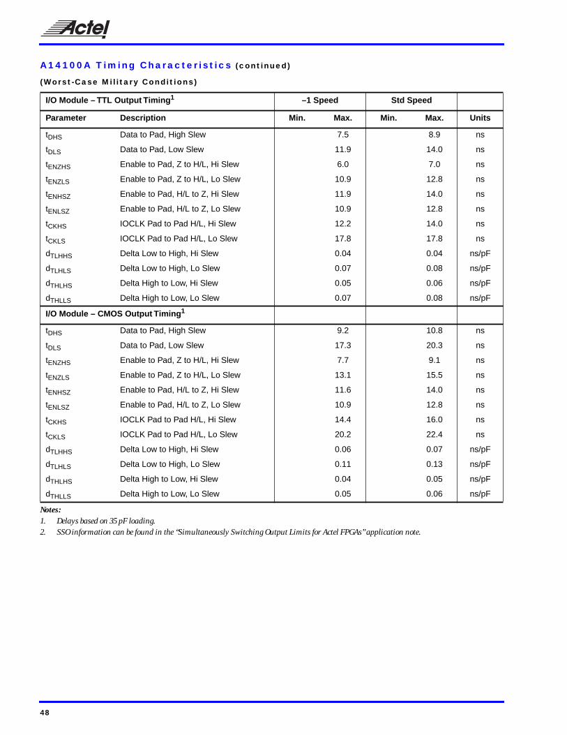
A14100A Timing Characteristics (continued)
(Worst-Case Military Conditions)
Notes:1. Delays based on 35 pF loading.2. SSO information can be found in the “Simultaneously Switching Output Limits for Actel FPGAs” application note.
I/O Module – TTL Output Timing 1 –1 Speed Std Speed
Parameter Description Min. Max. Min. Max. Units
tDHS Data to Pad, High Slew 7.5 8.9 ns
tDLS Data to Pad, Low Slew 11.9 14.0 ns
tENZHS Enable to Pad, Z to H/L, Hi Slew 6.0 7.0 ns
tENZLS Enable to Pad, Z to H/L, Lo Slew 10.9 12.8 ns
tENHSZ Enable to Pad, H/L to Z, Hi Slew 11.9 14.0 ns
tENLSZ Enable to Pad, H/L to Z, Lo Slew 10.9 12.8 ns
tCKHS IOCLK Pad to Pad H/L, Hi Slew 12.2 14.0 ns
tCKLS IOCLK Pad to Pad H/L, Lo Slew 17.8 17.8 ns
dTLHHS Delta Low to High, Hi Slew 0.04 0.04 ns/pF
dTLHLS Delta Low to High, Lo Slew 0.07 0.08 ns/pF
dTHLHS Delta High to Low, Hi Slew 0.05 0.06 ns/pF
dTHLLS Delta High to Low, Lo Slew 0.07 0.08 ns/pF
I/O Module – CMOS Output Timing 1
tDHS Data to Pad, High Slew 9.2 10.8 ns
tDLS Data to Pad, Low Slew 17.3 20.3 ns
tENZHS Enable to Pad, Z to H/L, Hi Slew 7.7 9.1 ns
tENZLS Enable to Pad, Z to H/L, Lo Slew 13.1 15.5 ns
tENHSZ Enable to Pad, H/L to Z, Hi Slew 11.6 14.0 ns
tENLSZ Enable to Pad, H/L to Z, Lo Slew 10.9 12.8 ns
tCKHS IOCLK Pad to Pad H/L, Hi Slew 14.4 16.0 ns
tCKLS IOCLK Pad to Pad H/L, Lo Slew 20.2 22.4 ns
dTLHHS Delta Low to High, Hi Slew 0.06 0.07 ns/pF
dTLHLS Delta Low to High, Lo Slew 0.11 0.13 ns/pF
dTHLHS Delta High to Low, Hi Slew 0.04 0.05 ns/pF
dTHLLS Delta High to Low, Lo Slew 0.05 0.06 ns/pF
48
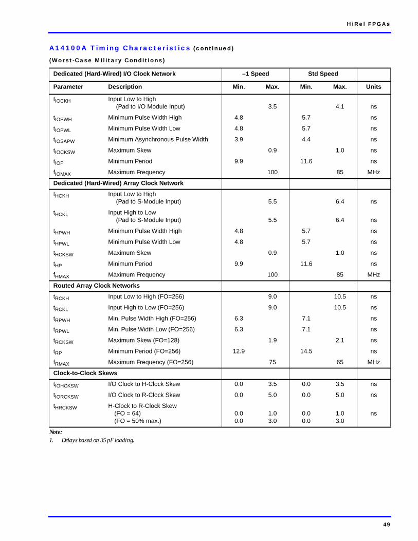
HiRel FPGAs
A14100A Timing Characteristics (continued)
(Worst-Case Military Conditions)
Note:1. Delays based on 35 pF loading.
Dedicated (Hard-Wired) I/O Clock Network –1 Speed Std Speed
Parameter Description Min. Max. Min. Max. Units
tIOCKH Input Low to High (Pad to I/O Module Input) 3.5 4.1 ns
tIOPWH Minimum Pulse Width High 4.8 5.7 ns
tIOPWL Minimum Pulse Width Low 4.8 5.7 ns
tIOSAPW Minimum Asynchronous Pulse Width 3.9 4.4 ns
tIOCKSW Maximum Skew 0.9 1.0 ns
tIOP Minimum Period 9.9 11.6 ns
fIOMAX Maximum Frequency 100 85 MHz
Dedicated (Hard-Wired) Array Clock Network
tHCKH Input Low to High (Pad to S-Module Input) 5.5 6.4 ns
tHCKL Input High to Low (Pad to S-Module Input) 5.5 6.4 ns
tHPWH Minimum Pulse Width High 4.8 5.7 ns
tHPWL Minimum Pulse Width Low 4.8 5.7 ns
tHCKSW Maximum Skew 0.9 1.0 ns
tHP Minimum Period 9.9 11.6 ns
fHMAX Maximum Frequency 100 85 MHz
Routed Array Clock Networks
tRCKH Input Low to High (FO=256) 9.0 10.5 ns
tRCKL Input High to Low (FO=256) 9.0 10.5 ns
tRPWH Min. Pulse Width High (FO=256) 6.3 7.1 ns
tRPWL Min. Pulse Width Low (FO=256) 6.3 7.1 ns
tRCKSW Maximum Skew (FO=128) 1.9 2.1 ns
tRP Minimum Period (FO=256) 12.9 14.5 ns
fRMAX Maximum Frequency (FO=256) 75 65 MHz
Clock-to-Clock Skews
tIOHCKSW I/O Clock to H-Clock Skew 0.0 3.5 0.0 3.5 ns
tIORCKSW I/O Clock to R-Clock Skew 0.0 5.0 0.0 5.0 ns
tHRCKSW H-Clock to R-Clock Skew (FO = 64)(FO = 50% max.)
0.00.0
1.03.0
0.00.0
1.03.0
ns
49
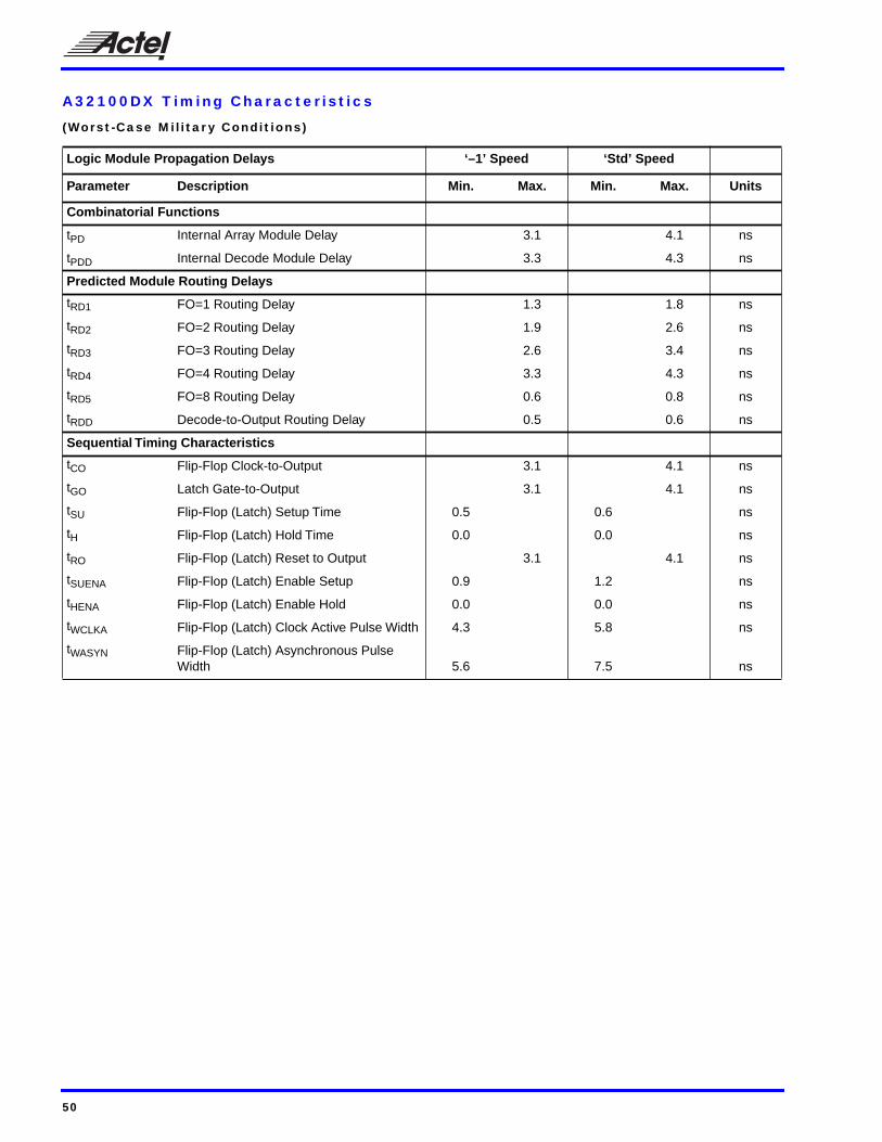
A32100DX Timing Characteristics
(Worst-Case Military Conditions)
Logic Module Propagation Delays ‘–1’ Speed ‘Std’ Speed
Parameter Description Min. Max. Min. Max. Units
Combinatorial Functions
tPD Internal Array Module Delay 3.1 4.1 ns
tPDD Internal Decode Module Delay 3.3 4.3 ns
Predicted Module Routing Delays
tRD1 FO=1 Routing Delay 1.3 1.8 ns
tRD2 FO=2 Routing Delay 1.9 2.6 ns
tRD3 FO=3 Routing Delay 2.6 3.4 ns
tRD4 FO=4 Routing Delay 3.3 4.3 ns
tRD5 FO=8 Routing Delay 0.6 0.8 ns
tRDD Decode-to-Output Routing Delay 0.5 0.6 ns
Sequential Timing Characteristics
tCO Flip-Flop Clock-to-Output 3.1 4.1 ns
tGO Latch Gate-to-Output 3.1 4.1 ns
tSU Flip-Flop (Latch) Setup Time 0.5 0.6 ns
tH Flip-Flop (Latch) Hold Time 0.0 0.0 ns
tRO Flip-Flop (Latch) Reset to Output 3.1 4.1 ns
tSUENA Flip-Flop (Latch) Enable Setup 0.9 1.2 ns
tHENA Flip-Flop (Latch) Enable Hold 0.0 0.0 ns
tWCLKA Flip-Flop (Latch) Clock Active Pulse Width 4.3 5.8 ns
tWASYN Flip-Flop (Latch) Asynchronous Pulse Width 5.6 7.5 ns
50
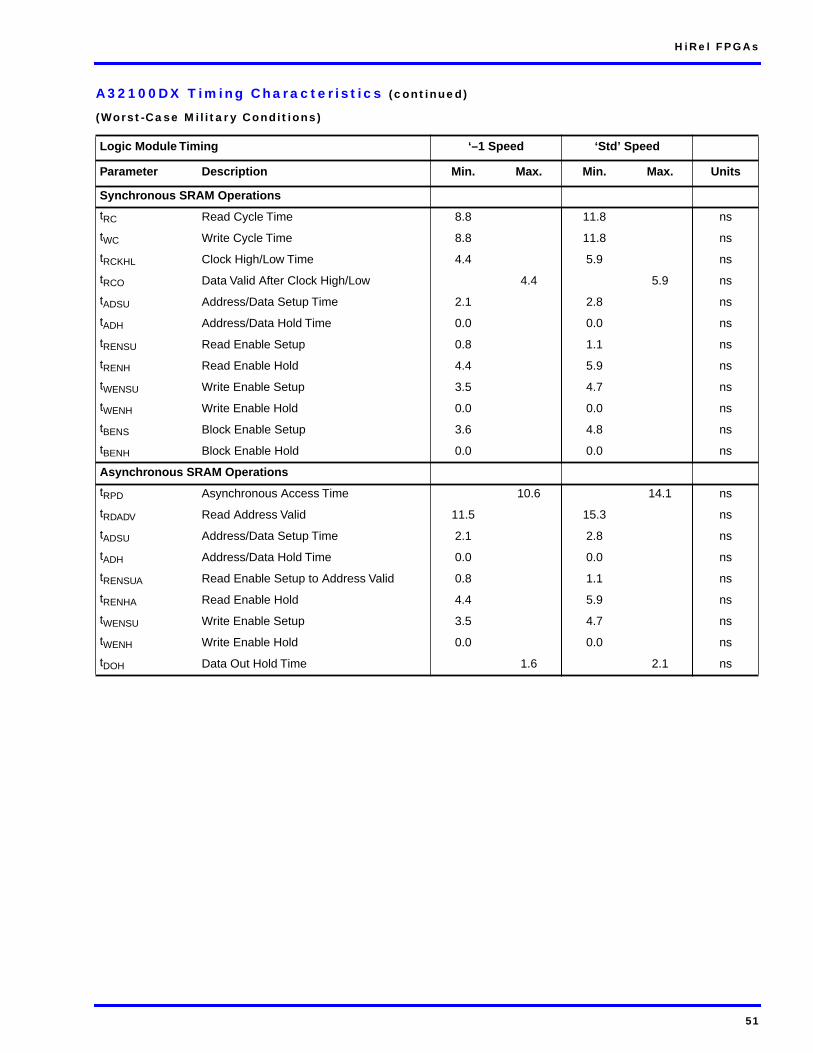
HiRel FPGAs
A32100DX Timing Characteristics (continued)
(Worst-Case Military Conditions)
Logic Module Timing ‘–1 Speed ‘Std’ Speed
Parameter Description Min. Max. Min. Max. Units
Synchronous SRAM Operations
tRC Read Cycle Time 8.8 11.8 ns
tWC Write Cycle Time 8.8 11.8 ns
tRCKHL Clock High/Low Time 4.4 5.9 ns
tRCO Data Valid After Clock High/Low 4.4 5.9 ns
tADSU Address/Data Setup Time 2.1 2.8 ns
tADH Address/Data Hold Time 0.0 0.0 ns
tRENSU Read Enable Setup 0.8 1.1 ns
tRENH Read Enable Hold 4.4 5.9 ns
tWENSU Write Enable Setup 3.5 4.7 ns
tWENH Write Enable Hold 0.0 0.0 ns
tBENS Block Enable Setup 3.6 4.8 ns
tBENH Block Enable Hold 0.0 0.0 ns
Asynchronous SRAM Operations
tRPD Asynchronous Access Time 10.6 14.1 ns
tRDADV Read Address Valid 11.5 15.3 ns
tADSU Address/Data Setup Time 2.1 2.8 ns
tADH Address/Data Hold Time 0.0 0.0 ns
tRENSUA Read Enable Setup to Address Valid 0.8 1.1 ns
tRENHA Read Enable Hold 4.4 5.9 ns
tWENSU Write Enable Setup 3.5 4.7 ns
tWENH Write Enable Hold 0.0 0.0 ns
tDOH Data Out Hold Time 1.6 2.1 ns
51
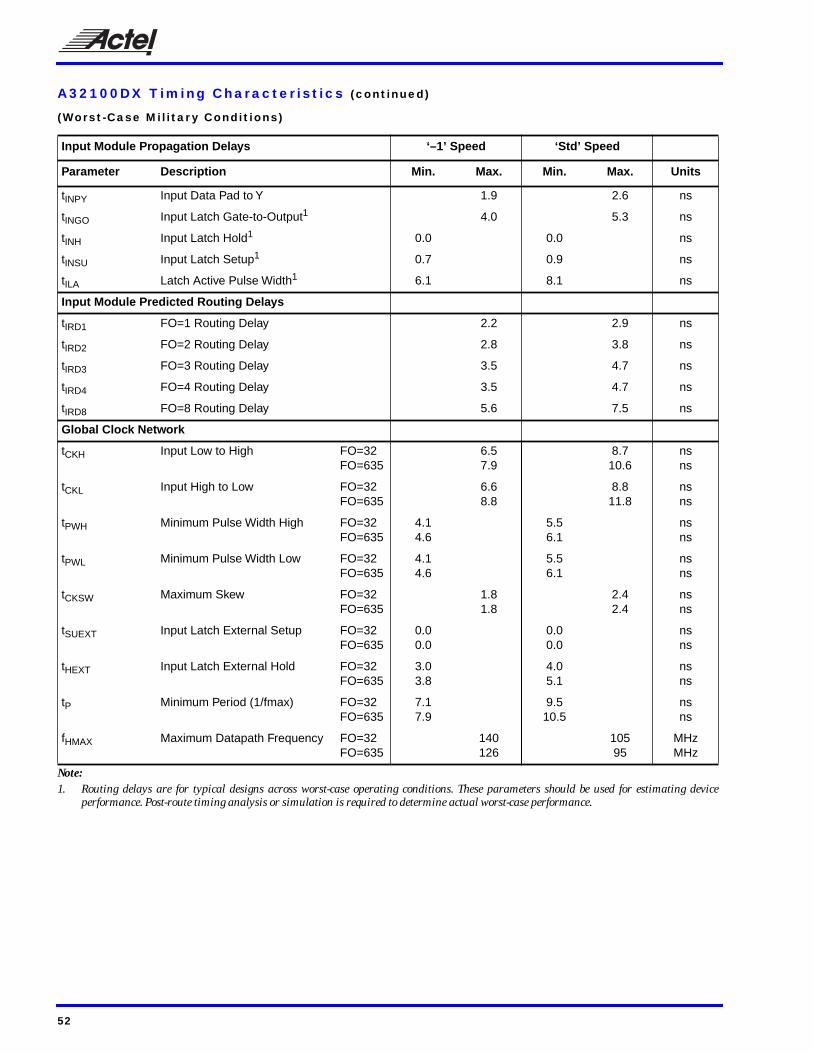
A32100DX Timing Characteristics (continued)
(Worst-Case Military Conditions)
Note:1. Routing delays are for typical designs across worst-case operating conditions. These parameters should be used for estimating device
performance. Post-route timing analysis or simulation is required to determine actual worst-case performance.
Input Module Propagation Delays ‘–1’ Speed ‘Std’ Speed
Parameter Description Min. Max. Min. Max. Units
tINPY Input Data Pad to Y 1.9 2.6 ns
tINGO Input Latch Gate-to-Output1 4.0 5.3 ns
tINH Input Latch Hold1 0.0 0.0 ns
tINSU Input Latch Setup1 0.7 0.9 ns
tILA Latch Active Pulse Width1 6.1 8.1 ns
Input Module Predicted Routing Delays
tIRD1 FO=1 Routing Delay 2.2 2.9 ns
tIRD2 FO=2 Routing Delay 2.8 3.8 ns
tIRD3 FO=3 Routing Delay 3.5 4.7 ns
tIRD4 FO=4 Routing Delay 3.5 4.7 ns
tIRD8 FO=8 Routing Delay 5.6 7.5 ns
Global Clock Network
tCKH Input Low to High FO=32FO=635
6.57.9
8.710.6
nsns
tCKL Input High to Low FO=32FO=635
6.68.8
8.811.8
nsns
tPWH Minimum Pulse Width High FO=32FO=635
4.14.6
5.56.1
nsns
tPWL Minimum Pulse Width Low FO=32FO=635
4.14.6
5.56.1
nsns
tCKSW Maximum Skew FO=32FO=635
1.81.8
2.42.4
nsns
tSUEXT Input Latch External Setup FO=32FO=635
0.00.0
0.00.0
nsns
tHEXT Input Latch External Hold FO=32FO=635
3.03.8
4.05.1
nsns
tP Minimum Period (1/fmax) FO=32FO=635
7.17.9
9.510.5
nsns
fHMAX Maximum Datapath Frequency FO=32FO=635
140126
10595
MHzMHz
52

HiRel FPGAs
A32100DX Timing Characteristics (continued)
(Worst-Case Military Conditions)
Notes:1. Routing delays are for typical designs across worst-case operating conditions. These parameters should be used for estimating device
performance. Post-route timing analysis or simulation is required to determine actual worst-case performance.2. SSO information can be found in the “Simultaneously Switching Output Limits for Actel FPGAs” application note.
Output Module Timing ‘–1’ Speed ‘Std’ Speed
Parameter Description Min. Max. Min. Max. Units
TTL Output Module Timing 1
tDLH Data to Pad High 5.1 6.8 ns
tDHL Data to Pad Low 6.3 8.3 ns
tENZH Enable Pad Z to High 6.6 8.8 ns
tENZL Enable Pad Z to Low 7.1 9.4 ns
tENHZ Enable Pad High to Z 11.5 15.3 ns
tENLZ Enable Pad Low to Z 11.5 15.3 ns
tGLH G to Pad High 11.5 15.3 ns
tGHL G to Pad Low 12.4 16.6 ns
tLSU I/O Latch Output Setup 0.4 0.5 ns
tLH I/O Latch Output Hold 0.0 0.0 ns
tLCO I/O Latch Clock-Out (Pad-to-Pad) 32 I/O 11.5 15.4 ns
tACO Array Latch Clock-Out (Pad-to-Pad) 32 I/O 16.3 21.7 ns
dTLH Capacitive Loading, Low to High 0.04 0.06 ns/pF
dTHL Capacitive Loading, High to Low 0.06 0.08 ns/pF
tWDO Hard-Wired Wide Decode Output 0.05 0.07 ns
CMOS Output Module Timing 1
tDLH Data to Pad High 6.3 8.3 ns
tDHL Data to Pad Low 5.1 6.8 ns
tENZH Enable Pad Z to High 6.6 8.8 ns
tENZL Enable Pad Z to Low 7.1 9.4 ns
tENHZ Enable Pad High to Z 11.5 15.3 ns
tENLZ Enable Pad Low to Z 11.5 15.3 ns
tGLH G to Pad High 11.5 15.3 ns
tGHL G to Pad Low 12.4 16.6 ns
tLSU I/O Latch Setup 0.4 0.5 ns
tLH I/O Latch Hold 0.0 0.0 ns
tLCO I/O Latch Clock-Out (Pad-to-Pad) 32 I/O 13.7 18.2 ns
tACO Array Latch Clock-Out (Pad-to-Pad) 32 I/O 19.2 25.6 ns
dTLH Capacitive Loading, Low to High 0.06 0.08 ns/pF
dTHL Capacitive Loading, High to Low 0.05 0.07 ns/pF
tWDO Hard-Wired Wide Decode Output 0.05 0.07 ns
53

A32200DX Timing Characteristics
(Worst-Case Military Conditions)
Logic Module Propagation Delays ‘–1 Speed ‘Std’ Speed
Parameter Description Min. Max. Min. Max. Units
Combinatorial Functions
tPD Internal Array Module Delay 2.8 3.8 ns
tPDD Internal Decode Module Delay 3.4 4.6 ns
Predicted Module Routing Delays
tRD1 FO=1 Routing Delay 1.6 2.1 ns
tRD2 FO=2 Routing Delay 2.3 3.1 ns
tRD3 FO=3 Routing Delay 2.9 3.9 ns
tRD4 FO=4 Routing Delay 3.5 4.7 ns
tRD5 FO=8 Routing Delay 6.2 8.2 ns
tRDD Decode-to-Output Routing Delay 0.8 1.1 ns
Sequential Timing Characteristics
tCO Flip-Flop Clock-to-Output 3.2 4.2 ns
tGO Latch Gate-to-Output 2.8 3.8 ns
tSU Flip-Flop (Latch) Setup Time 0.5 0.6 ns
tH Flip-Flop (Latch) Hold Time 0.0 0.0 ns
tRO Flip-Flop (Latch) Reset to Output 3.2 4.2 ns
tSUENA Flip-Flop (Latch) Enable Setup 0.9 1.2 ns
tHENA Flip-Flop (Latch) Enable Hold 0.0 0.0 ns
tWCLKA Flip-Flop (Latch) Clock Active Pulse Width 4.3 5.8 ns
tWASYN Flip-Flop (Latch) Asynchronous Pulse Width 5.7 7.6 ns
54

HiRel FPGAs
A32200DX Timing Characteristics (continued)
(Worst-Case Military Conditions)
Logic Module Timing ‘–1 Speed ‘Std’ Speed
Parameter Description Min. Max. Min. Max. Units
Synchronous SRAM Operations
tRC Read Cycle Time 8.8 11.8 ns
tWC Write Cycle Time 8.8 11.8 ns
tRCKHL Clock High/Low Time 4.4 5.9 ns
tRCO Data Valid After Clock High/Low 4.4 5.9 ns
tADSU Address/Data Setup Time 2.1 2.8 ns
tADH Address/Data Hold Time 0.0 0.0 ns
tRENSU Read Enable Setup 0.8 1.1 ns
tRENH Read Enable Hold 4.4 5.9 ns
tWENSU Write Enable Setup 3.5 4.7 ns
tWENH Write Enable Hold 0.0 0.0 ns
tBENS Block Enable Setup 3.6 4.8 ns
tBENH Block Enable Hold 0.0 0.0 ns
Asynchronous SRAM Operations
tRPD Asynchronous Access Time 10.6 14.1 ns
tRDADV Read Address Valid 11.5 15.3 ns
tADSU Address/Data Setup Time 2.1 2.8 ns
tADH Address/Data Hold Time 0.0 0.0 ns
tRENSUA Read Enable Setup to Address Valid 0.8 1.1 ns
tRENHA Read Enable Hold 4.4 5.9 ns
tWENSU Write Enable Setup 3.5 4.7 ns
tWENH Write Enable Hold 0.0 0.0 ns
tDOH Data Out Hold Time 1.6 2.1 ns
55
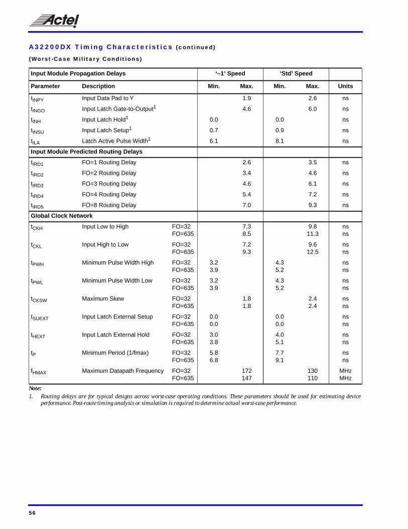
A32200DX Timing Characteristics (continued)
(Worst-Case Military Conditions)
Note:1. Routing delays are for typical designs across worst-case operating conditions. These parameters should be used for estimating device
performance. Post-route timing analysis or simulation is required to determine actual worst-case performance.
Input Module Propagation Delays ‘–1’ Speed ‘Std’ Speed
Parameter Description Min. Max. Min. Max. Units
tINPY Input Data Pad to Y 1.9 2.6 ns
tINGO Input Latch Gate-to-Output1 4.6 6.0 ns
tINH Input Latch Hold1 0.0 0.0 ns
tINSU Input Latch Setup1 0.7 0.9 ns
tILA Latch Active Pulse Width1 6.1 8.1 ns
Input Module Predicted Routing Delays
tIRD1 FO=1 Routing Delay 2.6 3.5 ns
tIRD2 FO=2 Routing Delay 3.4 4.6 ns
tIRD3 FO=3 Routing Delay 4.6 6.1 ns
tIRD4 FO=4 Routing Delay 5.4 7.2 ns
tIRD5 FO=8 Routing Delay 7.0 9.3 ns
Global Clock Network
tCKH Input Low to High FO=32FO=635
7.38.5
9.811.3
nsns
tCKL Input High to Low FO=32FO=635
7.29.3
9.612.5
nsns
tPWH Minimum Pulse Width High FO=32FO=635
3.23.9
4.35.2
nsns
tPWL Minimum Pulse Width Low FO=32FO=635
3.23.9
4.35.2
nsns
tCKSW Maximum Skew FO=32FO=635
1.81.8
2.42.4
nsns
tSUEXT Input Latch External Setup FO=32FO=635
0.00.0
0.00.0
nsns
tHEXT Input Latch External Hold FO=32FO=635
3.03.8
4.05.1
nsns
tP Minimum Period (1/fmax) FO=32FO=635
5.86.8
7.79.1
nsns
fHMAX Maximum Datapath Frequency FO=32FO=635
172147
130110
MHzMHz
56
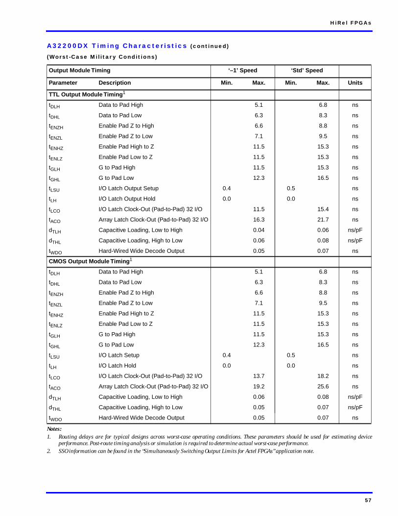
HiRel FPGAs
A32200DX Timing Characteristics (continued)
(Worst-Case Military Conditions)
Notes:1. Routing delays are for typical designs across worst-case operating conditions. These parameters should be used for estimating device
performance. Post-route timing analysis or simulation is required to determine actual worst-case performance.2. SSO information can be found in the “Simultaneously Switching Output Limits for Actel FPGAs” application note.
Output Module Timing ‘–1’ Speed ‘Std’ Speed
Parameter Description Min. Max. Min. Max. Units
TTL Output Module Timing 1
tDLH Data to Pad High 5.1 6.8 ns
tDHL Data to Pad Low 6.3 8.3 ns
tENZH Enable Pad Z to High 6.6 8.8 ns
tENZL Enable Pad Z to Low 7.1 9.5 ns
tENHZ Enable Pad High to Z 11.5 15.3 ns
tENLZ Enable Pad Low to Z 11.5 15.3 ns
tGLH G to Pad High 11.5 15.3 ns
tGHL G to Pad Low 12.3 16.5 ns
tLSU I/O Latch Output Setup 0.4 0.5 ns
tLH I/O Latch Output Hold 0.0 0.0 ns
tLCO I/O Latch Clock-Out (Pad-to-Pad) 32 I/O 11.5 15.4 ns
tACO Array Latch Clock-Out (Pad-to-Pad) 32 I/O 16.3 21.7 ns
dTLH Capacitive Loading, Low to High 0.04 0.06 ns/pF
dTHL Capacitive Loading, High to Low 0.06 0.08 ns/pF
tWDO Hard-Wired Wide Decode Output 0.05 0.07 ns
CMOS Output Module Timing 1
tDLH Data to Pad High 5.1 6.8 ns
tDHL Data to Pad Low 6.3 8.3 ns
tENZH Enable Pad Z to High 6.6 8.8 ns
tENZL Enable Pad Z to Low 7.1 9.5 ns
tENHZ Enable Pad High to Z 11.5 15.3 ns
tENLZ Enable Pad Low to Z 11.5 15.3 ns
tGLH G to Pad High 11.5 15.3 ns
tGHL G to Pad Low 12.3 16.5 ns
tLSU I/O Latch Setup 0.4 0.5 ns
tLH I/O Latch Hold 0.0 0.0 ns
tLCO I/O Latch Clock-Out (Pad-to-Pad) 32 I/O 13.7 18.2 ns
tACO Array Latch Clock-Out (Pad-to-Pad) 32 I/O 19.2 25.6 ns
dTLH Capacitive Loading, Low to High 0.06 0.08 ns/pF
dTHL Capacitive Loading, High to Low 0.05 0.07 ns/pF
tWDO Hard-Wired Wide Decode Output 0.05 0.07 ns
57

Package Pin Assignments
84-Pin CPGA (Top View)
Notes:1. MODE should be terminated to GND through a 10K resistor to enable Actionprobe usage, otherwise it can be terminated directly to GND.2. Unused I/O pins are designated as outputs by ALS and are driven low.3. All unassigned pins are available for use as I/Os
Function A1010B Pin Number A1020B Pin Number
CLK or I/O F9 F9
DCLK or I/O C10 C10
GND B7, E2, E3, F10, G10, K5 B7, E2, E3, F10, G10, K5
MODE E11 E11
N/C (No Connection) B1, B2, C1, C2, C11, D10, D11, J2, J10, K1, K10, K11, L1
B2
PRA or I/O A11 A11
PRB or I/O B10 B10
SDI or I/O B11 B11
VCC B5, E9, E10, F1, G2, K2, K7 B5, E9, E10, F1, G2, K2, K7
Orientation Pin (C3)
A
B
C
D
E
F
G
H
J
K
L
1 2 3 4 5 6 7 8 9 10 11
1 2 3 4 5 6 7 8 9 10 11
84-PinCPGA
A
B
C
D
E
F
G
H
J
K
L
58
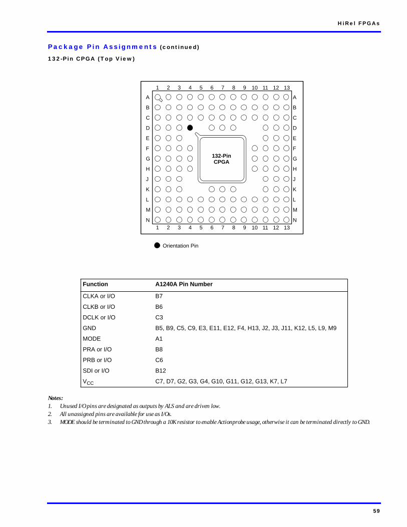
HiRel FPGAs
Package Pin Assignments (continued)
132-Pin CPGA (Top View)
Notes:1. Unused I/O pins are designated as outputs by ALS and are driven low.2. All unassigned pins are available for use as I/Os.3. MODE should be terminated to GND through a 10K resistor to enable Actionprobe usage, otherwise it can be terminated directly to GND.
Function A1240A Pin Number
CLKA or I/O B7
CLKB or I/O B6
DCLK or I/O C3
GND B5, B9, C5, C9, E3, E11, E12, F4, H13, J2, J3, J11, K12, L5, L9, M9
MODE A1
PRA or I/O B8
PRB or I/O C6
SDI or I/O B12
VCC C7, D7, G2, G3, G4, G10, G11, G12, G13, K7, L7
1 2 3 4 5 6 7 8 9 10 11 12 13
1 2 3 4 5 6 7 8 9 10 11 12 13
A
B
C
D
E
F
G
H
J
K
L
M
N
A
B
C
D
E
F
G
H
J
K
L
M
N
Orientation Pin
132-PinCPGA
59
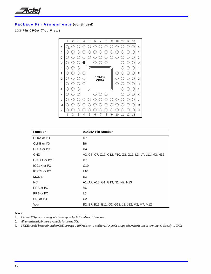
Package Pin Assignments (continued)
133-Pin CPGA (Top View)
Notes:1. Unused I/O pins are designated as outputs by ALS and are driven low.2. All unassigned pins are available for use as I/Os.3. MODE should be terminated to GND through a 10K resistor to enable Actionprobe usage, otherwise it can be terminated directly to GND.
Function A1425A Pin Number
CLKA or I/O D7
CLKB or I/O B6
DCLK or I/O D4
GND A2, C3, C7, C11, C12, F10, G3, G11, L3, L7, L11, M3, N12
HCLKA or I/O K7
IOCLK or I/O C10
IOPCL or I/O L10
MODE E3
NC A1, A7, A13, G1, G13, N1, N7, N13
PRA or I/O A6
PRB or I/O L6
SDI or I/O C2
VCC B2, B7, B12, E11, G2, G12, J2, J12, M2, M7, M12
1 2 3 4 5 6 7 8 9 10 11 12 13
A
B
C
D
E
F
G
H
J
K
L
M
N
133-PinCPGA
A
B
C
D
E
F
G
H
J
K
L
M
N
1 2 3 4 5 6 7 8 9 10 11 12 13
60

HiRel FPGAs
Package Pin Assignments (continued)
176-Pin CPGA (Top View)
Notes:1. Unused I/O pins are designated as outputs by ALS and are driven low.2. All unassigned pins are available for use as I/Os.3. MODE should be terminated to GND through a 10K resistor to enable Actionprobe usage, otherwise it can be terminated directly to GND.
Function A1280A, A1280XL Pin Number
CLKA or I/O A9
CLKB or I/O B8
DCLK or I/O B3
GND C8, D4, D6, D10, D12, E4, E12, F12, G4, H4, H12, J12, J13, K4, K12, L4, M4, M6, M8, M10, M12
MODE C3
PRA or I/O C9
PRB or I/O D7
SDI or I/O B14
VCC D5, D8, D11, F4, G12, H2, H3, H13, H14, J4, J14, M5, M11, N8
1
A
2 3 4 5 6 7 8 9 10 11
B
C
D
E
F
G
H
J
K
L
176-PinCPGA
1 2 3 4 5 6 7 8 9 10 11
12
12
13
13
14
14
15
15
M
N
P
R
A
B
C
D
E
F
G
H
J
K
L
M
N
P
R
61
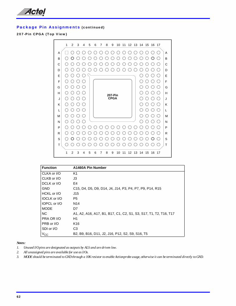
Package Pin Assignments (continued)
207-Pin CPGA (Top View)
Notes:1. Unused I/O pins are designated as outputs by ALS and are driven low.2. All unassigned pins are available for use as I/Os.3. MODE should be terminated to GND through a 10K resistor to enable Actionprobe usage, otherwise it can be terminated directly to GND.
Function A1460A Pin Number
CLKA or I/O K1CLKB or I/O J3DCLK or I/O E4GND C15, D4, D5, D9, D14, J4, J14, P3, P4, P7, P9, P14, R15HCKL or I/O J15IOCLK or I/O P5IOPCL or I/O N14MODE D7NC A1, A2, A16, A17, B1, B17, C1, C2, S1, S3, S17, T1, T2, T16, T17PRA OR I/O H1PRB or I/O K16SDI or I/O C3VCC B2, B9, B16, D11, J2, J16, P12, S2, S9, S16, T5
1
A
B
C
D
E
F
G
H
J
K
L
M
N
P
R
S
T
2 3 4 5 6 7 8 9 10 11 12 13 14 15 16 17
1 2 3 4 5 6 7 8 9 10 11 12 13 14 15 16 17
A
B
C
D
E
F
G
H
J
K
L
M
N
P
R
S
T
207-PinCPGA
62

HiRel FPGAs
Package Pin Assignments (continued)
257-Pin CPGA (Top View)
Notes:1. Unused I/O pins are designated as outputs by ALS and are driven low.2. All unassigned pins are available for use as I/Os.3. MODE should be terminated to GND through a 10K resistor to enable Actionprobe usage, otherwise it can be terminated directly to GND.
Function A14100A Pin Number
CLKA or I/O L4CLKB or I/O L5DCLK or I/O E4GND B16, C4, D4, D10, D16, E11, J5, K4, K16, L15, R4, T4, T10, T16, T17, X7HCLK or I/O J16IOCLK or I/O T5IOPCL or I/O R16MODE A5NC E5PRA OR I/O J1PRB or I/O J17SDI or I/O B4VCC C3, C10, C13, C17, K3, K17, V3, V7, V10, V17, X14
A
B
C
D
E
F
G
H
J
K
L
M
N
P
R
T
V
X
Y
A
B
C
D
E
F
G
H
J
K
L
M
N
P
R
T
V
X
Y
1 2 3 4 5 6 7 8 9 10 11 12 13 14 15 16 17 18 19
1 2 3 4 5 6 7 8 9 10 11 12 13 14 15 16 17 18 19
257-PinCPGA
63

Package Pin Assignments (continued)
84-Pin CQFP (Top View)
Notes:1. MODE should be terminated to GND through a 10K resistor to enable Actionprobe usage, otherwise it can be terminated directly to GND.2. Unused I/O pins are designated as outputs by ALS and are driven low.3. All unassigned pins are available for use as I/Os
Function A1020B Pin Number
CLKA or I/O 53DCLK or I/O 62GND 7, 8, 29, 49, 50, 71MODE 55N/C (No Connection) 1PRA or I/O 63PRB or I/O 64SDI or I/O 61VCC 14, 15, 22, 35, 56, 57, 77
Pin #1Index
123456789
101112131415161718192021
636261605958575655545352515049484746454443
22 23 24 25 26 27 28 29 30 31 32 33 34 35 36 37 38 39 40 41 42
84 83 82 81 80 79 78 77 76 75 74 73 72 71 70 69 68 67 66 65 64
84-PinCQFP
64
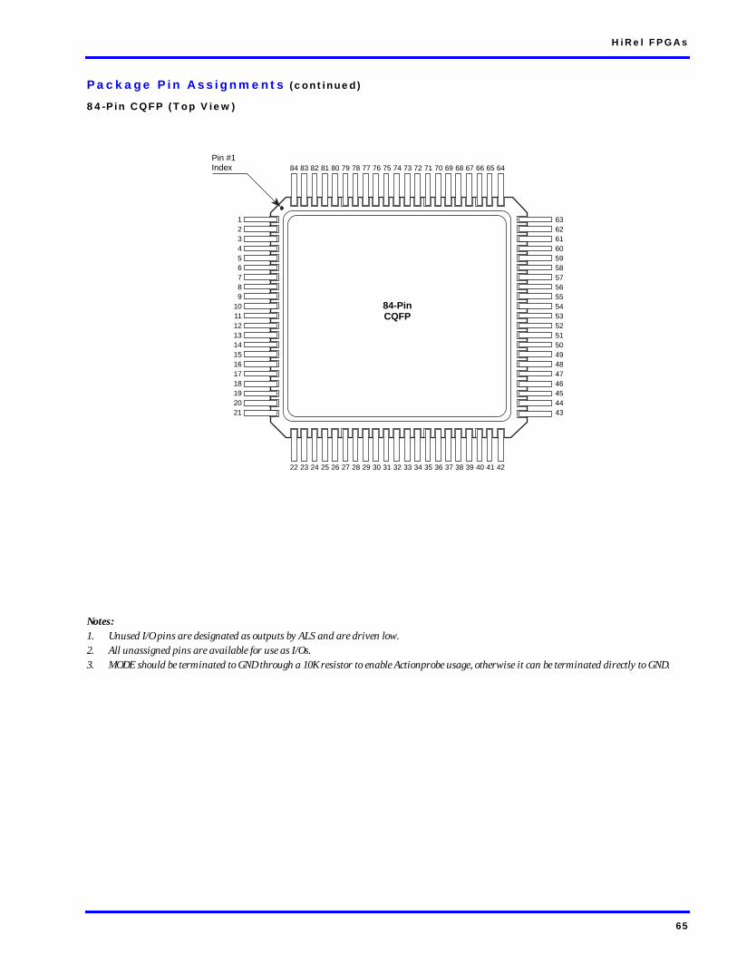
HiRel FPGAs
Package Pin Assignments (continued)
84-Pin CQFP (Top View)
Notes:1. Unused I/O pins are designated as outputs by ALS and are driven low.2. All unassigned pins are available for use as I/Os.3. MODE should be terminated to GND through a 10K resistor to enable Actionprobe usage, otherwise it can be terminated directly to GND.
Pin #1Index
123456789
101112131415161718192021
636261605958575655545352515049484746454443
22 23 24 25 26 27 28 29 30 31 32 33 34 35 36 37 38 39 40 41 42
84 83 82 81 80 79 78 77 76 75 74 73 72 71 70 69 68 67 66 65 64
84-PinCQFP
65
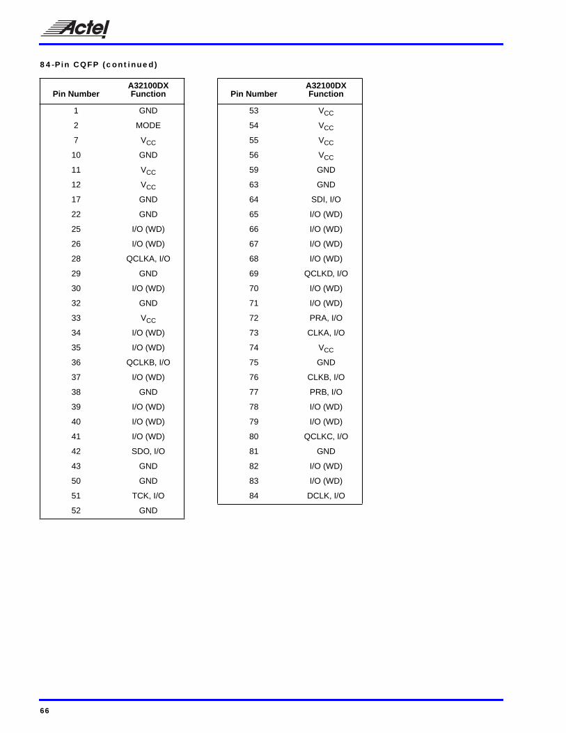
84-Pin CQFP (continued)
Pin NumberA32100DXFunction Pin Number
A32100DXFunction
1 GND 53 VCC
2 MODE 54 VCC
7 VCC 55 VCC
10 GND 56 VCC
11 VCC 59 GND
12 VCC 63 GND
17 GND 64 SDI, I/O
22 GND 65 I/O (WD)
25 I/O (WD) 66 I/O (WD)
26 I/O (WD) 67 I/O (WD)
28 QCLKA, I/O 68 I/O (WD)
29 GND 69 QCLKD, I/O
30 I/O (WD) 70 I/O (WD)
32 GND 71 I/O (WD)
33 VCC 72 PRA, I/O
34 I/O (WD) 73 CLKA, I/O
35 I/O (WD) 74 VCC
36 QCLKB, I/O 75 GND
37 I/O (WD) 76 CLKB, I/O
38 GND 77 PRB, I/O
39 I/O (WD) 78 I/O (WD)
40 I/O (WD) 79 I/O (WD)
41 I/O (WD) 80 QCLKC, I/O
42 SDO, I/O 81 GND
43 GND 82 I/O (WD)
50 GND 83 I/O (WD)
51 TCK, I/O 84 DCLK, I/O
52 GND
66

HiRel FPGAs
Package Pin Assignments (continued)
132-Pin CQFP (Top View)
Notes:1. Unused I/O pins are designated as outputs by ALS and are driven low.2. All unassigned pins are available for use as I/Os.3. MODE should be terminated to GND through a 10K resistor to enable Actionprobe usage, otherwise it can be terminated directly to GND.
Function A1425A Pin Number
CLKA or I/O 116CLKB or I/O 117DCLK or I/O 131GND 2, 10, 26, 36, 42, 58, 65, 74, 90, 92, 101, 106, 122HCLK or I/O 50IOCLK or I/O 98IOPCL or I/O 64MODE 9NC 1, 34, 66, 67, 99, 100, 132PRA or I/O 118PRB or I/O 48SDI or I/O 3VCC 11, 22, 27, 43, 59, 75, 78, 89, 91, 107, 123
132-PinCQFP
Pin #1Index
132 131 130 129 128 127 126 125 124 107 106 105 104 103 102 101 100
34 35 36 37 38 39 40 41 42 59 60 61 62 63 64 65 66
67
68
69
70
71
72
73
74
75
92
93
94
95
96
97
98
99
33
32
31
30
29
28
27
26
25
8
7
6
5
4
3
2
1
67
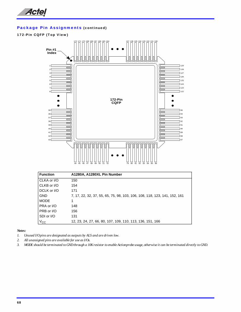
Package Pin Assignments (continued)
172-Pin CQFP (Top View)
Notes:1. Unused I/O pins are designated as outputs by ALS and are driven low.2. All unassigned pins are available for use as I/Os.3. MODE should be terminated to GND through a 10K resistor to enable Actionprobe usage, otherwise it can be terminated directly to GND.
Function A1280A, A1280XL Pin Number
CLKA or I/O 150CLKB or I/O 154DCLK or I/O 171GND 7, 17, 22, 32, 37, 55, 65, 75, 98, 103, 106, 108, 118, 123, 141, 152, 161MODE 1PRA or I/O 148PRB or I/O 156SDI or I/O 131VCC 12, 23, 24, 27, 66, 80, 107, 109, 110, 113, 136, 151, 166
172-PinCQFP
Pin #1Index
172 171 170 169 168 167 166 165 164 137 136 135 134 133 132 131 130
44 45 46 47 48 49 50 51 52 79 80 81 82 83 84 85 86
87
88
89
90
91
92
93
94
95
122
123
124
125
126
127
128
129
43
42
41
40
39
38
37
36
35
8
7
6
5
4
3
2
1
68

HiRel FPGAs
Package Pin Assignments (continued)
196-Pin CQFP (Top View)
Notes:1. Unused I/O pins are designated as outputs by ALS and are driven low.2. All unassigned pins are available for use as I/Os.3. MODE should be terminated to GND through a 10K resistor to enable Actionprobe usage, otherwise it can be terminated directly to GND.
Function A1460A Pin Number
CLKA or I/O 172CLKB or I/O 173DCLK or I/O 196GND 1, 13, 37, 51, 52, 64, 86, 98, 101, 112, 138, 139, 149, 162, 183, 193HCLK or I/O 77IOCLK or I/O 148IOPCL or I/O 100MODE 11PRA or I/O 174PRB or I/O 75SDI or I/O 2VCC 12, 38, 39, 59, 94, 110, 111, 137, 140, 155, 189
196-PinCQFP
Pin #1Index
196 195 194 193 192 191 190 189 188 155 154 153 152 151 150 149 148
50 51 52 53 54 55 56 57 58 91 92 93 94 95 96 97 98
99
100
101
102
103
104
105
106
107
140
141
142
143
144
145
146
147
49
48
47
46
45
44
43
42
41
8
7
6
5
4
3
2
1
69
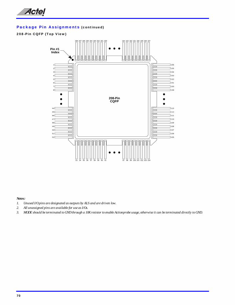
Package Pin Assignments (continued)
208-Pin CQFP (Top View)
Notes:1. Unused I/O pins are designated as outputs by ALS and are driven low.2. All unassigned pins are available for use as I/Os.3. MODE should be terminated to GND through a 10K resistor to enable Actionprobe usage, otherwise it can be terminated directly to GND.
208-PinCQFP
Pin #1Index
208 207 206 205 204 203 202 201 200 164 163 162 161 160 159 158 157
53 54 55 56 57 58 59 60 61 97 98 99 100 101 102 103 104
105
106
107
108
109
110
111
112
113
149
150
151
152
153
154
155
156
52
51
50
49
48
47
46
45
44
8
7
6
5
4
3
2
1
70
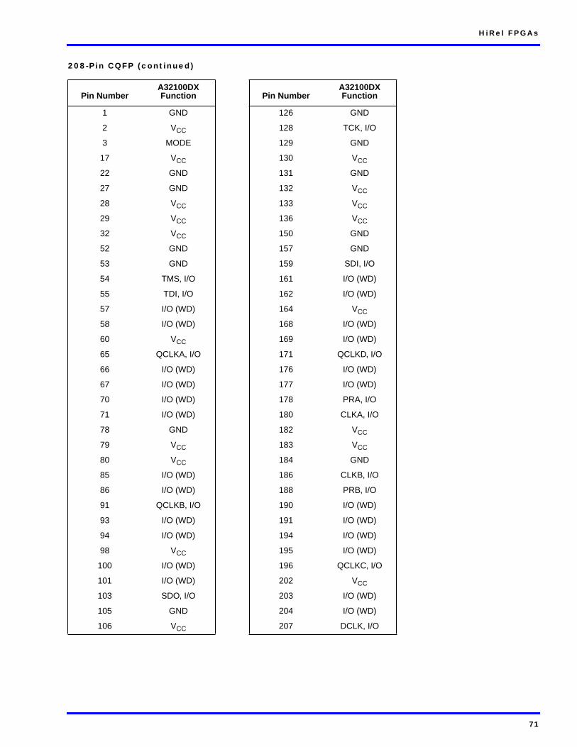
HiRel FPGAs
208-Pin CQFP (continued)
Pin NumberA32100DXFunction Pin Number
A32100DXFunction
1 GND 126 GND
2 VCC 128 TCK, I/O
3 MODE 129 GND
17 VCC 130 VCC
22 GND 131 GND
27 GND 132 VCC
28 VCC 133 VCC
29 VCC 136 VCC
32 VCC 150 GND
52 GND 157 GND
53 GND 159 SDI, I/O
54 TMS, I/O 161 I/O (WD)
55 TDI, I/O 162 I/O (WD)
57 I/O (WD) 164 VCC
58 I/O (WD) 168 I/O (WD)
60 VCC 169 I/O (WD)
65 QCLKA, I/O 171 QCLKD, I/O
66 I/O (WD) 176 I/O (WD)
67 I/O (WD) 177 I/O (WD)
70 I/O (WD) 178 PRA, I/O
71 I/O (WD) 180 CLKA, I/O
78 GND 182 VCC
79 VCC 183 VCC
80 VCC 184 GND
85 I/O (WD) 186 CLKB, I/O
86 I/O (WD) 188 PRB, I/O
91 QCLKB, I/O 190 I/O (WD)
93 I/O (WD) 191 I/O (WD)
94 I/O (WD) 194 I/O (WD)
98 VCC 195 I/O (WD)
100 I/O (WD) 196 QCLKC, I/O
101 I/O (WD) 202 VCC
103 SDO, I/O 203 I/O (WD)
105 GND 204 I/O (WD)
106 VCC 207 DCLK, I/O
71
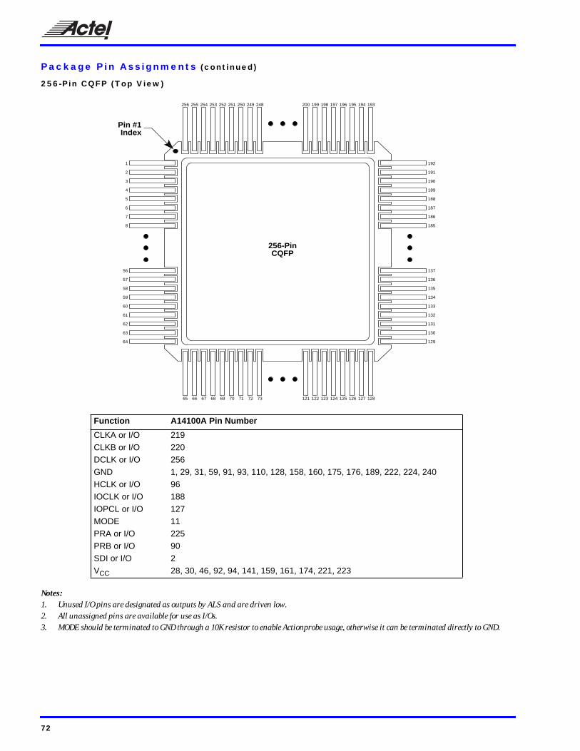
Package Pin Assignments (continued)
256-Pin CQFP (Top View)
Notes:1. Unused I/O pins are designated as outputs by ALS and are driven low.2. All unassigned pins are available for use as I/Os.3. MODE should be terminated to GND through a 10K resistor to enable Actionprobe usage, otherwise it can be terminated directly to GND.
Function A14100A Pin Number
CLKA or I/O 219CLKB or I/O 220DCLK or I/O 256GND 1, 29, 31, 59, 91, 93, 110, 128, 158, 160, 175, 176, 189, 222, 224, 240HCLK or I/O 96IOCLK or I/O 188IOPCL or I/O 127MODE 11PRA or I/O 225PRB or I/O 90SDI or I/O 2VCC 28, 30, 46, 92, 94, 141, 159, 161, 174, 221, 223
256-PinCQFP
Pin #1Index
256 255 254 253 252 251 250 249 248 200 199 198 197 196 195 194 193
65 66 67 68 69 70 71 72 73 121 122 123 124 125 126 127 128
129
130
131
132
133
134
135
136
137
185
186
187
188
189
190
191
192
64
63
62
61
60
59
58
57
56
8
7
6
5
4
3
2
1
72
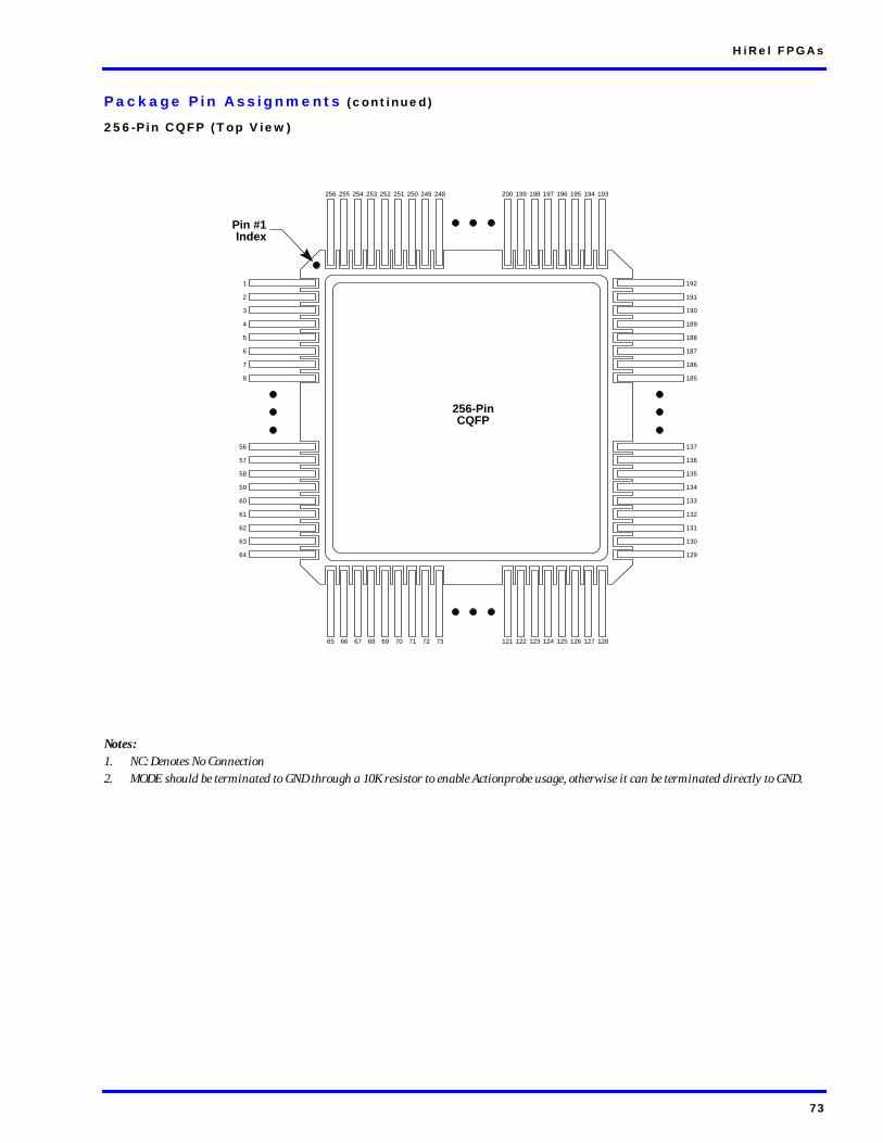
HiRel FPGAs
Package Pin Assignments (continued)
256-Pin CQFP (Top View)
Notes:1. NC: Denotes No Connection2. MODE should be terminated to GND through a 10K resistor to enable Actionprobe usage, otherwise it can be terminated directly to GND.
256-PinCQFP
Pin #1Index
256 255 254 253 252 251 250 249 248 200 199 198 197 196 195 194 193
65 66 67 68 69 70 71 72 73 121 122 123 124 125 126 127 128
129
130
131
132
133
134
135
136
137
185
186
187
188
189
190
191
192
64
63
62
61
60
59
58
57
56
8
7
6
5
4
3
2
1
73
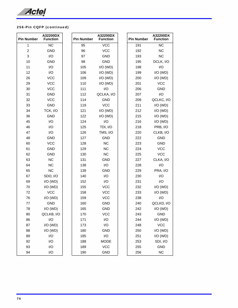
256-Pin CQFP (continued)
Pin NumberA32200DXFunction Pin Number
A32200DXFunction Pin Number
A32200DXFunction
1 NC 95 VCC 191 NC
2 GND 96 VCC 192 NC
3 I/O 97 GND 193 NC
10 GND 98 GND 195 DCLK, I/O
11 I/O 105 I/O (WD) 198 I/O
12 I/O 106 I/O (WD) 199 I/O (WD)
26 VCC 109 I/O (WD) 200 I/O (WD)
29 VCC 110 I/O (WD) 201 VCC
30 VCC 111 I/O 206 GND
31 GND 112 QCLKA, I/O 207 I/O
32 VCC 114 GND 209 QCLKC, I/O
33 GND 119 VCC 211 I/O (WD)
34 TCK, I/O 121 I/O (WD) 212 I/O (WD)
36 GND 122 I/O (WD) 215 I/O (WD)
45 I/O 124 I/O 216 I/O (WD)
46 I/O 125 TDI, I/O 218 PRB, I/O
47 I/O 126 TMS, I/O 220 CLKB, I/O
48 GND 127 GND 222 GND
60 VCC 128 NC 223 GND
61 GND 129 NC 224 VCC
62 GND 130 NC 225 VCC
63 NC 131 GND 227 CLKA, I/O
64 NC 138 I/O 228 I/O
65 NC 139 GND 229 PRA, I/O
67 SDO, I/O 140 I/O 230 I/O
69 I/O (WD) 152 I/O 231 I/O
70 I/O (WD) 155 VCC 232 I/O (WD)
72 VCC 158 VCC 233 I/O (WD)
76 I/O (WD) 159 VCC 238 I/O
77 GND 160 GND 240 QCLKD, I/O
78 I/O (WD) 165 GND 242 I/O (WD)
80 QCLKB, I/O 170 VCC 243 GND
86 I/O 171 I/O 244 I/O (WD)
87 I/O (WD) 173 I/O 248 VCC
88 I/O (WD) 180 GND 250 I/O (WD)
89 I/O 185 I/O 251 I/O (WD)
92 I/O 188 MODE 253 SDI, I/O
93 I/O 189 VCC 255 GND
94 I/O 190 GND 256 NC
74

HiRel FPGAs
Package Mechanical Drawings
133-Pin Ceramic Pin Grid Array (CPGA)
Notes:1. All dimensions are in inches unless otherwise stated.2. BSC—Basic Spacing between Centers.
1.360" ± 0.015" square 0.120"0.140"
0.100" BSC
0.018" ± 0.002"
0.050" ± 0.010"
Pin #1
1.200" BSC
0.100"0.130"
0.045"0.055"
Orientation Pin
11 12 1310987654321
N
M
L
K
J
H
G
F
E
D
C
B
A
75
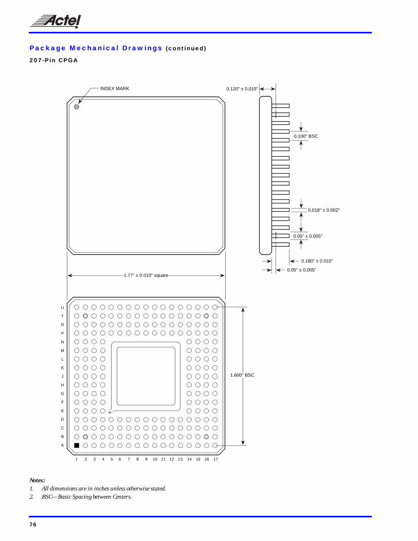
Package Mechanical Drawings (continued)
207-Pin CPGA
Notes:1. All dimensions are in inches unless otherwise stated.2. BSC—Basic Spacing between Centers.
INDEX MARK
0.100" BSC
0.120" ± 0.015"
11 12 13 14 15 16 1710987654321
U
T
R
P
N
M
L
K
J
H
G
F
E
D
C
B
A
1.600" BSC
0.018" ± 0.002"
0.180" ± 0.010"
0.05" ± 0.005"1.77" ± 0.010" square
0.05" ± 0.005"
76
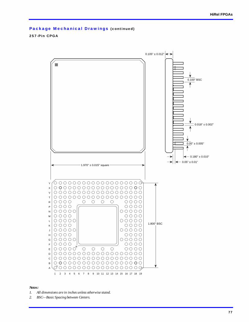
HiRel FPGAs
Package Mechanical Drawings (continued)
257-Pin CPGA
Notes:1. All dimensions are in inches unless otherwise stated.2. BSC—Basic Spacing between Centers.
0.105" ± 0.012"
0.05" ± 0.005"
0.100" BSC
Y
X
V
T
R
P
N
M
L
K
J
H
G
F
E
D
C
B
A
1 2 3 4 5 6 7 8 9 10 11 12 13 14 15 16 17 18 19
0.018" ± 0.002"
0.180" ± 0.010"
0.05" ± 0.01"1.970" ± 0.015" square
1.800" BSC
77
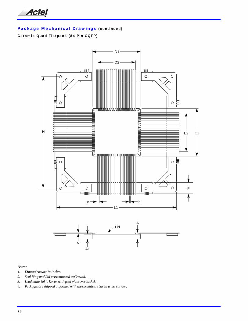
Package Mechanical Drawings (continued)
Ceramic Quad Flatpack (84-Pin CQFP)
Notes:1. Dimensions are in inches.2. Seal Ring and Lid are connected to Ground.3. Lead material is Kovar with gold plate over nickel.4. Packages are shipped unformed with the ceramic tie bar in a test carrier.
D2
D1
e
A1
A
c
H E2 E1
b
L1
F
Lid
78
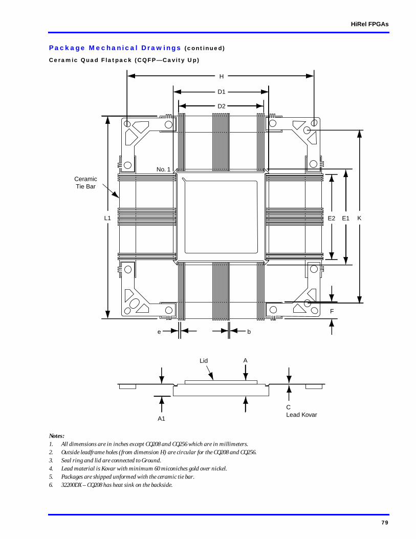
HiRel FPGAs
Package Mechanical Drawings (continued)
Ceramic Quad Flatpack (CQFP—Cavity Up)
Notes:1. All dimensions are in inches except CQ208 and CQ256 which are in millimeters.2. Outside leadframe holes (from dimension H) are circular for the CQ208 and CQ256.3. Seal ring and lid are connected to Ground.4. Lead material is Kovar with minimum 60 miconiches gold over nickel.5. Packages are shipped unformed with the ceramic tie bar. 6. 32200DX – CQ208 has heat sink on the backside.
A
b
H
D1
D2
E2 E1
F
L1 K
CeramicTie Bar
No. 1
e
A1
CLead Kovar
Lid
79
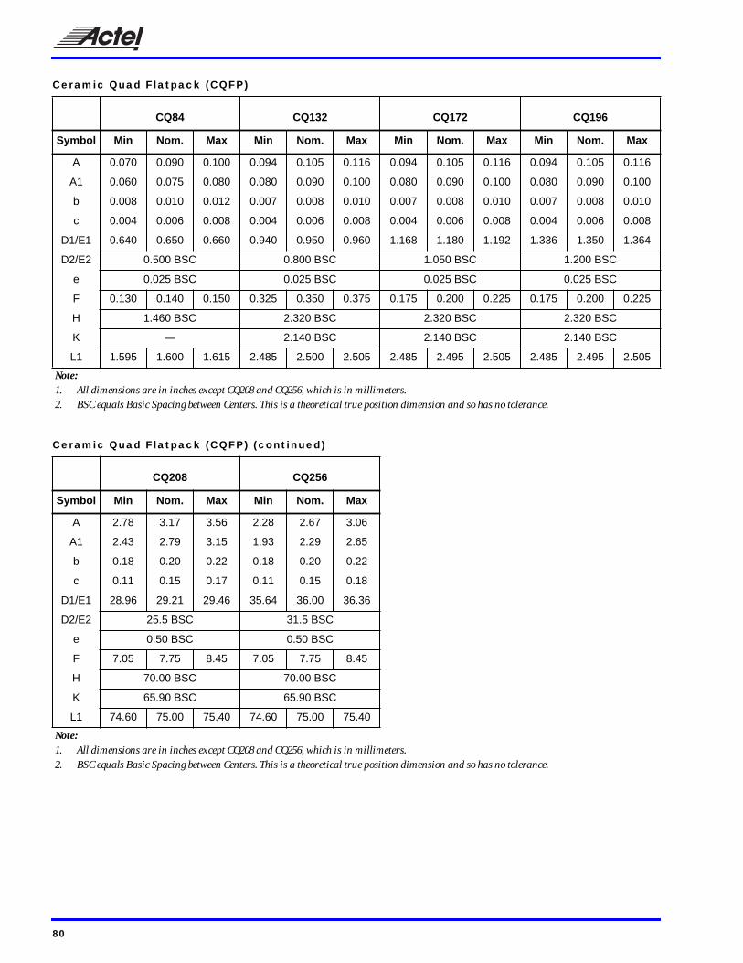
Ceramic Quad Flatpack (CQFP)
CQ84 CQ132 CQ172 CQ196
Symbol Min Nom. Max Min Nom. Max Min Nom. Max Min Nom. Max
A 0.070 0.090 0.100 0.094 0.105 0.116 0.094 0.105 0.116 0.094 0.105 0.116
A1 0.060 0.075 0.080 0.080 0.090 0.100 0.080 0.090 0.100 0.080 0.090 0.100
b 0.008 0.010 0.012 0.007 0.008 0.010 0.007 0.008 0.010 0.007 0.008 0.010
c 0.004 0.006 0.008 0.004 0.006 0.008 0.004 0.006 0.008 0.004 0.006 0.008
D1/E1 0.640 0.650 0.660 0.940 0.950 0.960 1.168 1.180 1.192 1.336 1.350 1.364
D2/E2 0.500 BSC 0.800 BSC 1.050 BSC 1.200 BSC
e 0.025 BSC 0.025 BSC 0.025 BSC 0.025 BSC
F 0.130 0.140 0.150 0.325 0.350 0.375 0.175 0.200 0.225 0.175 0.200 0.225
H 1.460 BSC 2.320 BSC 2.320 BSC 2.320 BSC
K — 2.140 BSC 2.140 BSC 2.140 BSC
L1 1.595 1.600 1.615 2.485 2.500 2.505 2.485 2.495 2.505 2.485 2.495 2.505
Note:1. All dimensions are in inches except CQ208 and CQ256, which is in millimeters.2. BSC equals Basic Spacing between Centers. This is a theoretical true position dimension and so has no tolerance.
Ceramic Quad Flatpack (CQFP) (continued)
CQ208 CQ256
Symbol Min Nom. Max Min Nom. Max
A 2.78 3.17 3.56 2.28 2.67 3.06
A1 2.43 2.79 3.15 1.93 2.29 2.65
b 0.18 0.20 0.22 0.18 0.20 0.22
c 0.11 0.15 0.17 0.11 0.15 0.18
D1/E1 28.96 29.21 29.46 35.64 36.00 36.36
D2/E2 25.5 BSC 31.5 BSC
e 0.50 BSC 0.50 BSC
F 7.05 7.75 8.45 7.05 7.75 8.45
H 70.00 BSC 70.00 BSC
K 65.90 BSC 65.90 BSC
L1 74.60 75.00 75.40 74.60 75.00 75.40
Note:1. All dimensions are in inches except CQ208 and CQ256, which is in millimeters.2. BSC equals Basic Spacing between Centers. This is a theoretical true position dimension and so has no tolerance.
80

HiRel FPGAs
81

Actel and the Actel logo are registered trademarks of Actel Corporation.
All other trademarks are the property of their owners.
http://www.actel.com
Actel Europe Ltd.Daneshill House, Lutyens CloseBasingstoke, Hampshire RG24 8AGUnited KingdomTel: +44.(0)1256.305600Fax: +44.(0)1256.355420
Actel Corporation955 East Arques AvenueSunnyvale, California 94086USATel: 408.739.1010Fax: 408.739.1540
Actel Asia-PacificEXOS Ebisu Bldg. 4F1-24-14 Ebisu Shibuya-kuTokyo 150 JapanTel: +81.(0)3.3445.7671Fax: +81.(0)3.3445.7668
5192641-1/1.99
Related Documents