NANO EXPRESS Highly Uniform Epitaxial ZnO Nanorod Arrays for Nanopiezotronics J. Volk Æ T. Nagata Æ R. Erde ´lyi Æ I. Ba ´rsony Æ A. L. To ´th Æ I. E. Luka ´cs Æ Zs. Cziga ´ny Æ H. Tomimoto Æ Y. Shingaya Æ T. Chikyow Received: 14 January 2009 / Accepted: 24 March 2009 / Published online: 7 April 2009 Ó to the authors 2009 Abstract Highly uniform and c-axis-aligned ZnO nano- rod arrays were fabricated in predefined patterns by a low temperature homoepitaxial aqueous chemical method. The nucleation seed patterns were realized in polymer and in metal thin films, resulting in, all-ZnO and bottom-con- tacted structures, respectively. Both of them show excellent geometrical uniformity: the cross-sectional uniformity according to the scanning electron micrographs across the array is lower than 2%. The diameter of the hexagonal prism-shaped nanorods can be set in the range of 90– 170 nm while their typical length achievable is 0.5– 2.3 lm. The effect of the surface polarity was also exam- ined, however, no significant difference was found between the arrays grown on Zn-terminated and on O-terminated face of the ZnO single crystal. The transmission electron microscopy observation revealed the single crystalline nature of the nanorods. The current–voltage characteristics taken on an individual nanorod contacted by a Au-coated atomic force microscope tip reflected Schottky-type behavior. The geometrical uniformity, the designable pat- tern, and the electrical properties make the presented nanorod arrays ideal candidates to be used in ZnO-based DC nanogenerator and in next-generation integrated pie- zoelectric nano-electromechanical systems (NEMS). Keywords Aqueous chemical growth Vertical nanowire Nanogenerator NEMS Piezoelectricity Rod-type photonic crystal Introduction Vertically aligned ZnO nanorods (NRs) and nanowires (NWs) are attracting much interest for several applications such as nanophotonics [1, 2], dye-sensitized solar cells [3, 4], electron field emitters [5, 6], surround-gate field effect transistors [7], and nanopiezotronics [8]. A number of preparation methods by high temperature vapor transport [9] and low temperature chemical synthesis [10, 11] were developed. For comparison, the NR arrays can be classified from several aspects: physical and geometrical properties of the individual building blocks and their uniformity in length, in diameter, and in axis-to-substrate angle. The NRs/NWs can be distributed either randomly or in a well- defined way. The above applications require different kinds of nanostructures concerning their geometrical parameters. For instance, photonic crystals with well-defined defects are of importance in nanophotonics [12, 13]. Another demanding application is the construction of ZnO NW- based DC current generator, where the NWs convert the mechanical energy of a vibrating Pt-coated, zig-zag-shaped electrode to electric energy by exploiting the piezoelectric nature of ZnO [14]. Even for nanosensors, however, the generated power density (*80 nW/cm 2 ) should be sig- nificantly increased. As Liu et al. [15] have pointed out the output voltage of the system, being now typically in the order of *10 mV, can be drastically improved by increasing the number of the active NW-s, i.e., the ones which are in continuously contact with the zigzag top electrode. Therefore, two approaches were proposed: J. Volk (&) R. Erde ´lyi I. Ba ´rsony A. L. To ´th I. E. Luka ´cs Zs. Cziga ´ny Research Institute for Technical Physics and Materials Science, Konkoly Thege Miklo ´s u ´t 29-33, 1121 Budapest, Hungary e-mail: [email protected] J. Volk T. Nagata H. Tomimoto Y. Shingaya T. Chikyow National Institute for Materials Science, 1-1 Namiki, Tsukuba, Ibaraki 305-0044, Japan 123 Nanoscale Res Lett (2009) 4:699–704 DOI 10.1007/s11671-009-9302-1

Welcome message from author
This document is posted to help you gain knowledge. Please leave a comment to let me know what you think about it! Share it to your friends and learn new things together.
Transcript
NANO EXPRESS
Highly Uniform Epitaxial ZnO Nanorod Arraysfor Nanopiezotronics
J. Volk Æ T. Nagata Æ R. Erdelyi Æ I. Barsony ÆA. L. Toth Æ I. E. Lukacs Æ Zs. Czigany ÆH. Tomimoto Æ Y. Shingaya Æ T. Chikyow
Received: 14 January 2009 / Accepted: 24 March 2009 / Published online: 7 April 2009
� to the authors 2009
Abstract Highly uniform and c-axis-aligned ZnO nano-
rod arrays were fabricated in predefined patterns by a low
temperature homoepitaxial aqueous chemical method. The
nucleation seed patterns were realized in polymer and in
metal thin films, resulting in, all-ZnO and bottom-con-
tacted structures, respectively. Both of them show excellent
geometrical uniformity: the cross-sectional uniformity
according to the scanning electron micrographs across the
array is lower than 2%. The diameter of the hexagonal
prism-shaped nanorods can be set in the range of 90–
170 nm while their typical length achievable is 0.5–
2.3 lm. The effect of the surface polarity was also exam-
ined, however, no significant difference was found between
the arrays grown on Zn-terminated and on O-terminated
face of the ZnO single crystal. The transmission electron
microscopy observation revealed the single crystalline
nature of the nanorods. The current–voltage characteristics
taken on an individual nanorod contacted by a Au-coated
atomic force microscope tip reflected Schottky-type
behavior. The geometrical uniformity, the designable pat-
tern, and the electrical properties make the presented
nanorod arrays ideal candidates to be used in ZnO-based
DC nanogenerator and in next-generation integrated pie-
zoelectric nano-electromechanical systems (NEMS).
Keywords Aqueous chemical growth �Vertical nanowire � Nanogenerator � NEMS �Piezoelectricity � Rod-type photonic crystal
Introduction
Vertically aligned ZnO nanorods (NRs) and nanowires
(NWs) are attracting much interest for several applications
such as nanophotonics [1, 2], dye-sensitized solar cells [3,
4], electron field emitters [5, 6], surround-gate field effect
transistors [7], and nanopiezotronics [8]. A number of
preparation methods by high temperature vapor transport
[9] and low temperature chemical synthesis [10, 11] were
developed. For comparison, the NR arrays can be classified
from several aspects: physical and geometrical properties
of the individual building blocks and their uniformity in
length, in diameter, and in axis-to-substrate angle. The
NRs/NWs can be distributed either randomly or in a well-
defined way. The above applications require different kinds
of nanostructures concerning their geometrical parameters.
For instance, photonic crystals with well-defined defects
are of importance in nanophotonics [12, 13]. Another
demanding application is the construction of ZnO NW-
based DC current generator, where the NWs convert the
mechanical energy of a vibrating Pt-coated, zig-zag-shaped
electrode to electric energy by exploiting the piezoelectric
nature of ZnO [14]. Even for nanosensors, however, the
generated power density (*80 nW/cm2) should be sig-
nificantly increased. As Liu et al. [15] have pointed out the
output voltage of the system, being now typically in the
order of *10 mV, can be drastically improved by
increasing the number of the active NW-s, i.e., the ones
which are in continuously contact with the zigzag top
electrode. Therefore, two approaches were proposed:
J. Volk (&) � R. Erdelyi � I. Barsony � A. L. Toth �I. E. Lukacs � Zs. Czigany
Research Institute for Technical Physics and Materials Science,
Konkoly Thege Miklos ut 29-33, 1121 Budapest, Hungary
e-mail: [email protected]
J. Volk � T. Nagata � H. Tomimoto � Y. Shingaya � T. Chikyow
National Institute for Materials Science, 1-1 Namiki,
Tsukuba, Ibaraki 305-0044, Japan
123
Nanoscale Res Lett (2009) 4:699–704
DOI 10.1007/s11671-009-9302-1

improving the uniformity of the NWs on one hand and
patterning the array according to the dimension and shape
of the top electrode. Vertical ZnO nanoarrays arranged in a
designed pattern were recently produced by a few groups
using different techniques [16, 17], however, either the
geometrical non-uniformity of the NWs or the low density
of the vertical microcrystals (*1 NR/lm2) makes their use
in nanogenerator application difficult. Moreover, if the
nanostructure is produced by vapor–liquid–solid (VLS)
method the metal catalyst droplet on the top of the NW can
hinder the formation of the required Schottky contact at the
top electrode/NW interface.
Here, we demonstrate alternative fabrication routes
which fulfill all the above crucial requirements by pro-
viding highly uniform, crystallographically oriented NRs in
the 100-nm diameter range, in predefined, dense patterns.
Our method benefits of the catalyst free, low temperature
epitaxial growth, and the direct writing nanolithography.
We have tried two options for the formation of NR arrays.
In the first, the desired nucleation pattern was drawn in a
polymethyl-methacrylate (PMMA) layer, which was sub-
sequently removed resulting in an all-ZnO structure. In the
second route, the nucleation pattern was realized in a hard
metal coating; therefore, the fabricated NRs were electri-
cally contacted at the anchoring surface.
Experimental
All ZnO NR Array
The process flow for the fabrication of all-ZnO NR arrays
is shown in Fig. 1a–d. At first, the Zn- and O-terminated
single crystal ZnO wafers were washed ultrasonically in
acetone, ethanol, and deionized water, which was followed
by a thermal-annealing step in a quartz tube at 1,050 �C for
8 h in oxygen atmosphere. In order to prevent the subli-
mation of Zn, the substrates were placed between yttrium
stabilized zirconia (YSZ) wafers before annealing. The
250-nm-thick PMMA resist layer was exposed by e-beam
lithography in an Elionix ELS-7500EX instrument
(Fig. 1b). Circular spots of different (50–100 nm) diame-
ters arranged in a triangular (TRI) or honeycomb (HC)
lattice were generated. They behave as active centers for
ZnO nanostructure growth in the PMMA layer. The growth
was effected by the aqueous chemical growth technique
(Fig. 1c). The aqueous bath contained the same (4 or
40 mM) molar amount of zinc nitrate hexahydrate
(Zn(NO3)2 � 6H2O) and hexamethylene tetramine
((CH2)6N4). During the ZnO nanostructure growth, the
specimen was mounted upside-down on a polytetrafluoro-
ethylene (PTFE) sample holder. The nanocrystal growth
was carried out—without an electric field applied—in a
multipurpose oven for 1–3.5 h periods at a set temperature
of 85 �C. However, due to the high heat capacity of the
glass container and the dry atmosphere, the warming up
was relatively slow: the bath temperature reached 80 and
82 �C after 2 and 3 h, respectively. Following slow cool-
ing, the sample was thoroughly washed in de-ionized water
and purged in nitrogen. Afterward, the PMMA layer was
removed in acetone. This step also helps to lift-off the
parasitic ZnO debris formed in the solution volume
(Fig. 1d).
Anchored NR Array
Nanorods grown through a hard metal mask obtained by
Ar-ion milling are anchored in the single crystal substrate
in the recessed dips etched during metal milling. Thereby
the fabrication of arrays of electrically contacted NRs is
achieved. The process shown in Fig. 1e–h is partly similar
to that of the previously introduced all-ZnO arrays. How-
ever, here the surface treatment process of ZnO substrate
was followed by the deposition of a 30-nm-thick, high-
quality Ru layer by using ion-beam sputtering [18]
(Fig. 1e). The pattern was formed first in PMMA by
e-beam lithography (Fig. 1f) and was transferred into the
hard metal film by Ar? ion milling (Fig. 1g). For the NR
synthesis, the same chemical growth method was used as
for the all-ZnO arrays (Fig. 1h). The preparation condition
details for both all-ZnO and anchored arrays are summa-
rized in Table 1.
Fig. 1 Schematic process flow of all-ZnO (a–d) and anchored (e–h)
nanorod arrays. The processing steps for all-ZnO structure are:
surface treatment of ZnO substrates (a), pattern generation in PMMA
by e-beam lithography (b), chemical nanowire growth (c), and
PMMA removal (d). Processing steps for the anchored ZnO array are:
Ru thin film deposition (e), e-beam lithography (f), Ar? ion milling
(g), and chemical nanorod growth after PMMA removal (h)
700 Nanoscale Res Lett (2009) 4:699–704
123

Characterization Methods
The obtained nanostructures were visualized by a Hitachi
S4800 field emission scanning electron microscope (FE-
SEM). Transmission electron microscope (TEM) images
were obtained by a 200 kV JEOL JEM-2010 instrument.
The electrical characterization of the individual NWs was
carried out in air by conductive AFM technique by means
of a SII NanoTechnology Inc., SPA-400 instrument
equipped with Keithley 4200-SCS semiconductor para-
metric analyzer. The spring constant and resonant
frequency of the used Au-coated cantilever is 1.4 N/m and
26 kHz, respectively.
Results and Discussion
The SEM images of the all-ZnO arrays fabricated at opti-
mized conditions are shown in Fig. 2a–c. The c-axis-
oriented NRs show hexagonal cross section, which are
according to the crystal orientation of the substrate col-
lectively aligned to each other. The sidewalls of the prism-
shaped rods correspond to the most stable non-polar
f1�100g faces. Note the *250 nm high bottleneck-shaped
part at the bottom of the nanocrystals in Fig. 2a, which was
formed inside the cylindrical hole developed in the PMMA
layer. We have found that by changing the template
geometry, the diameter and the length of the NRs can be
tuned in the range of 90–170 nm and 0.5–2.3 lm, respec-
tively. Detailed geometrical parameters for every specimen
are summarized in Table 1. The perpendicularly standing
NRs reflect excellent geometrical uniformity. According to
the image analysis done on the FESEM image (pixel size of
1.4 nm) shown in Fig. 2b, the average Feret’s diameter is
125 ± 2.1 nm. This is the diameter of a circle having the
same area as the hexagonal cross section of the object. It
corresponds to a relative deviation of *1.6% (Fig. 2b
inset). We have tried the same growth conditions on Zn-
and O-polar ZnO surfaces, but no significant difference
was found in the obtained arrays. A typical example
observed during the optimization of the growth parameters
is inserted in Fig. 2d. When the concentration in the growth
solution is increased to 40 mM, the growing NRs coalesce
at their non-polar sides to form a contiguous network.
Table 1 Summary of the growth parameters and the obtained nanorod dimensions
Type Surface
polarity
(Zn/O)
Hole diameter
(nm)
Inter-rod
distance
(nm)
Lattice
type
Nanorod
density
(NR/lm2)
Growth
concentration
(mM)
Growth
time
(min)
Feret’s
diameter
(nm)
Length
(lm)
Figures
All-ZnO O 75 263 HC 11 4 180 170 1.6 2a
All-ZnO Zn 100 200 TRI 29 4 60 125 0.5 2b
All-ZnO O 80 200 TRI 29 4 180 94 1.0 2c
All-ZnO Zn 100 350 HC 6 40 130 – 3.5 2d
Anchored Zn 100 350 HC 6 4 270 150 2.2 3a
Anchored Zn 75 263 HC 11 4 270 135 2.3 3b
Anchored Zn 50 175 HC 25 4 270 90 2.3 3c
Fig. 2 FESEM images on all-ZnO nanorod arrays prepared by soft-
masking method in honeycomb (a, d) and on triangular (b, c)
arrangements. The single crystal nanorods have hexagonal cross-
sections; the uniformity of diameter can be \2% (b inset). When the
concentration of the growth solution is increased to 40 mM, a
coalescence of nanorods is observed (d)
Nanoscale Res Lett (2009) 4:699–704 701
123
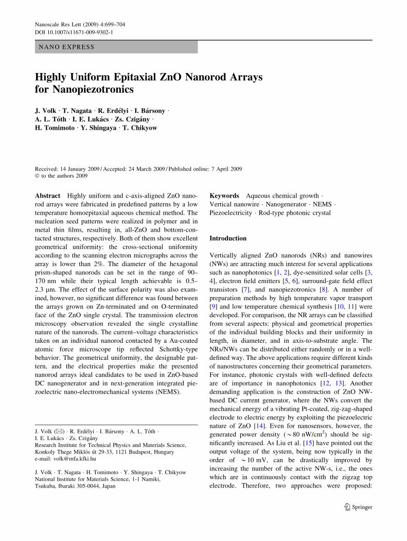
Anchored, i.e., metal back contacted arrays show similar
geometrical features as the all-ZnO structures (Fig. 3a, b).
Here, we have also downscaled the pattern: the densest
array had an rod-to-rod distance of 175 nm, which in HC
lattice corresponds to a NR density of 25 NR/lm. How-
ever, in the case of high aspect ratio (*26:1) and short rod-
to-rod distance, a self-attraction of NR tips occurs
(Fig. 3c).
Similar phenomenon was described by other groups, as
well, albeit they used high temperature vapor transport
methods. Wang et al. [19] explained the self-attraction by
the accumulated Coulomb charges at the NR/Au catalyst
droplet interface when charged by the primary electrons
during SEM observation. Han et al. [20] have also
observed self-attracted NWs prepared by catalyst-free
vapor–solid (VS) preparation method. Therefore, the
charging cannot be ascribed to the presence of catalysts.
In our case, the NR tip attachment can be attributed to
surface tension of water during the drying process, as it was
described by Segawa et al. [21] for hybrid organic–inor-
ganic NR. We believe that further down-scaling is limited
mainly by the resolution of our e-beam lithography facility
rather than by growth kinetics.
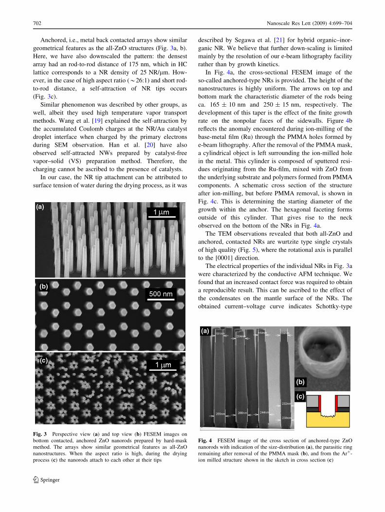
In Fig. 4a, the cross-sectional FESEM image of the
so-called anchored-type NRs is provided. The height of the
nanostructures is highly uniform. The arrows on top and
bottom mark the characteristic diameter of the rods being
ca. 165 ± 10 nm and 250 ± 15 nm, respectively. The
development of this taper is the effect of the finite growth
rate on the nonpolar faces of the sidewalls. Figure 4b
reflects the anomaly encountered during ion-milling of the
base-metal film (Ru) through the PMMA holes formed by
e-beam lithography. After the removal of the PMMA mask,
a cylindrical object is left surrounding the ion-milled hole
in the metal. This cylinder is composed of sputtered resi-
dues originating from the Ru-film, mixed with ZnO from
the underlying substrate and polymers formed from PMMA
components. A schematic cross section of the structure
after ion-milling, but before PMMA removal, is shown in
Fig. 4c. This is determining the starting diameter of the
growth within the anchor. The hexagonal faceting forms
outside of this cylinder. That gives rise to the neck
observed on the bottom of the NRs in Fig. 4a.
The TEM observations revealed that both all-ZnO and
anchored, contacted NRs are wurtzite type single crystals
of high quality (Fig. 5), where the rotational axis is parallel
to the [0001] direction.
The electrical properties of the individual NRs in Fig. 3a
were characterized by the conductive AFM technique. We
found that an increased contact force was required to obtain
a reproducible result. This can be ascribed to the effect of
the condensates on the mantle surface of the NRs. The
obtained current–voltage curve indicates Schottky-type
Fig. 3 Perspective view (a) and top view (b) FESEM images on
bottom contacted, anchored ZnO nanorods prepared by hard-mask
method. The arrays show similar geometrical features as all-ZnO
nanostructures. When the aspect ratio is high, during the drying
process (c) the nanorods attach to each other at their tips
Fig. 4 FESEM image of the cross section of anchored-type ZnO
nanorods with indication of the size-distribution (a), the parasitic ring
remaining after removal of the PMMA mask (b), and from the Ar?-
ion milled structure shown in the sketch in cross section (c)
702 Nanoscale Res Lett (2009) 4:699–704
123

behavior (Fig. 6), which can be originated either from the
contact between probe-tip and NR-tip or from the collar-
shaped ZnO/Ru interface at the bottom of the NR. How-
ever, as it was shown earlier [18] and found here as well,
the Ru/single crystal ZnO interface-contact has Ohmic
character. Therefore, the Au/ZnO NR contact is responsi-
ble for the observed rectifying behavior.
In order to correctly describe the electrical behavior by
an equivalent circuit and to separate the contributions of
contact resistance, internal resistance of the NR, surface
conductance, and piezoelectricity induced Schottky barrier
height change, a refinement of the measurement technique
and further systematic investigation is required. Still, in our
work the successful formation of a rectifying Schottky
contact between ZnO NR and the measuring tip could
reproducibly be obtained. This was pointed out by Liu et al.
[22] to be a necessary requirement for the operation of the
DC nanogenerator with vibrating top contact.
Conclusions
We have demonstrated that by using homoepitaxial chem-
ical growth method highly uniform, single crystalline NR
arrays arranged in a predefined pattern can be prepared. By
changing the growth parameters, diameter and length of the
NRs can be tuned in the range of 90–170 nm and 500 nm–
2.3 lm, respectively. The monodispersity of the diameter of
single crystalline NRs can be \2% by maintaining an
excellent uniformity in the longitudinal dimension. We
exploited two alternative synthesis routes using soft and
hard under-layer to obtain all-ZnO and metal contacted,
anchored NR arrays, respectively. The former one can be a
promising candidate for nanopillar-based photonic crystals,
especially if a refractive index contrast between the NR and
the ZnO substrate is realized. On the other hand, anchored
NR arrays contacted on the bottom are promising structures
for nanopiezotronics. The arrays show excellent uniformity
in length and the dense pattern (*30 NR/lm2) can be
adjusted to the top vibrating electrode of the nanogenerator.
Thereby a significant improvement in the output voltage,
hence a more efficient energy harvesting can be predicted.
Acknowledgments This work was supported by the ‘‘Nanotech-
nology Network Project’’ of the Ministry of Education, Culture,
Sports, Science and Technology (MEXT) in Japan, and by the Hun-
garian Fundamental Research Found (OTKA) under contract PD
77578. The authors are grateful to Prof. Y. Bando for the valuable
suggestions and to Mr. Y. Misawa, Mr. S. Hara, Mr. K. Tamura, and
Mr. A. Ohi for professional help with sample preparation.
References
1. M.H. Huang, S. Mao, H. Feick, H. Yan, Y. Wu, H. Kind,
E. Weber, R. Russo, P. Yang, Science 292, 1897 (2001). doi:
10.1126/science.1060367
2. R. Konenkap, R.C. Word, C. Schlegel, Appl. Phys. Lett. 85, 6004
(2004). doi:10.1063/1.1836873
3. M. Law, L.E. Greene, J.C. Johnson, R. Saykally, P. Yang, Nat.
Mater. 4, 455 (2005). doi:10.1038/nmat1387
4. J.B. Baxter, E.S. Aydil, Appl. Phys. Lett. 86, 053114 (2005). doi:
10.1063/1.1861510
5. Y.-K. Tseng, C.-J. Huang, H.-M. Cheng, I.-N. Lin, K.-S. Liu,
I.-C. Chen, Adv. Funct. Mater. 13, 811 (2003). doi:10.1002/adfm.
200304434
6. A. Wei, X.W. Sun, C.X. Xu, Z.L. Dong, M.B. Yu, W. Huang,
Appl. Phys. Lett. 88, 213102 (2006). doi:10.1063/1.2206249
7. H.T. Ng, J. Han, T. Yamada, P. Nguyen, Y.P. Chen, M. Mey-
yappan, Nano Lett. 4, 1247 (2004). doi:10.1021/nl049461z
8. Z.L. Wang, Adv. Mater. 19, 889 (2007). doi:10.1002/adma.
200602918
9. Z.Y. Fan, J.G. Lu, J. Nanosci, Nanotechnology 5, 1561 (2005).
doi:10.1166/jnn.2005.182
Fig. 5 The TEM observation reveals the single crystalline nature of
the nanorods. The fast growing [0001] crystallographic direction is
parallel to the longitudinal axis
Fig. 6 Current–voltage characteristic recorded on an individual
nanorod by conductive AFM. In order to obtain reproducible results
in air increased contact force is required, which can be ascribed to the
condensate formation on the nanorods (inset)
Nanoscale Res Lett (2009) 4:699–704 703
123

10. L. Vayssieres, K. Keis, S.-E. Lindquist, A. Hagfeldt, J. Phys.
Chem. B 105, 3350 (2001). doi:10.1021/jp010026s
11. B. Liu, H.C. Zeng, J. Am. Chem. Soc. 125, 4430 (2003). doi:
10.1021/ja0299452
12. M. Tokushima, H. Yamada, Y. Arakawa, Appl. Phys. Lett. 84,
4298 (2004). doi:10.1063/1.1755838
13. S.H.G. Teo, A.Q. Liu, J. Singh, M.B. Yu, G.Q. Lo, Appl. Phys.
A: Mater. Sci. Process. 89, 417 (2007). doi:10.1007/s00339-007-
4122-6
14. X. Wang, J. Song, J. Liu, Z.L. Wang, Science 316, 102 (2007).
doi:10.1126/science.1139366
15. J. Liu, P. Fei, J. Zhou, R. Tummala, Z.L. Wang, Appl. Phys. Lett.
92, 173105 (2008). doi:10.1063/1.2918840
16. J.H. He, J.H. Hsu, C.W. Wang, H.N. Lin, L.J. Chen, Z.L. Wang,
J. Phys. Chem. B 110, 50 (2006). doi:10.1021/jp055180j
17. Y.-J. Kim, C.-H. Lee, Y.J. Hong, G.-C. Yi, Appl. Phys. Lett. 89,
163128 (2006). doi:10.1063/1.2364162
18. T. Nagata, P. Ahmet, Y.Z. Yoo, K. Yamada, K. Tsutsui,
Y. Wada, T. Chikyow, Appl. Surf. Sci. 252, 2503 (2006). doi:
10.1016/j.apsusc.2005.05.085
19. X. Wang, C.J. Summers, Z.L. Wang, Appl. Phys. Lett. 86,
013111 (2005). doi:10.1063/1.1847713
20. X. Han, G. Wang, L. Zhou, J.G. Hou, Chem. Commun. 212
(2006). doi:10.1039/b512259g
21. H. Segawa, S. Yamaguchi, Y. Yamazaki, T. Yano, S. Shibata,
H. Misawa, Appl. Phys. A: Mater. Sci. Process. 83, 447 (2006).
doi:10.1007/s00339-006-3568-2
22. J. Liu, P. Fei, J. Song, X. Wang, C. Lao, R. Tummala, Z.L. Wang,
Nano Lett. 8, 328 (2008). doi:10.1021/nl0728470
704 Nanoscale Res Lett (2009) 4:699–704
123
Related Documents