14 Highly Energy-Efficient On-Chip Pulsed- Current-Mode Transmission Line Interconnect Tomoaki Maekawa, Shuhei Amakawa, Hiroyuki Ito, Noboru Ishihara, and Kazuya Masu Tokyo Institute of Technology Japan 1. Introduction System-on-a-chip (SoC) has become possible since a great number of circuit elements can be integrated into a single chip by the miniaturization technologies for Si CMOS. Network-on- Chip (NoC) has been investigated actively, and it is expected to be a new approach for designing the communication subsystems of SoC (Lee et al., 2008). Enormous circuit blocks are loaded onto the NoC, and on-chip networks like local area networks (LANs) in the NoC communicate among these circuit blocks. Since the performance of the NoC is strongly affected by on-chip networks, the construction of efficient on-chip communications infrastructures will be increasingly significant. Some of the important characteristics for on-chip interconnects are bandwidth, latency, and power. In particular, power saving technologies are very important in realizing Green IT (in- formation technology). Power dissipation in on-chip networks mainly occurs at interconnects due to the increase of wiring resistance and capacitance. A significant issue is that power consumption of conventional on-chip interconnects, i.e. so-called RC lines, is proportional to the signal frequency; hence, it is very difficult to reduce energy dissipation per bit. Given the recent trend of high-speed signaling, we have to solve this problem and offer some good solutions. One solution is the use of copper lines and low-k dielectric, and these techniques have been widely applied and reduce power consumption for transmitting signals. However long interconnects still consume large power as in the case of RC lines. Another solution is the introduction of on-chip transmission line interconnects (TLIs). The applications of TLIs have been widely demonstrated. Modulation (Chang et al., 2003), pulsed- current-mode (Jose et al., 2006), current-mode-logic (Ito et al., 2004, 2005; Ishii et al., 2006; Gomi et al., 2004), low voltage differential signaling (Ito et al., 2007) and multi-drop (Ito et al., 2008) techniques are proposed, and these techniques enable the improvement of bandwidth, latency and extensibility of on-chip networks. Figure 1 is an image of on-chip networks with TLIs. It is also reported that TLIs have a better power efficiency than the conventional on-chip lines as the line length and signal frequency increase (Ito et al., 2004; Gomi et al., 2004; Ito et al., 2005; Ishii et al., 2006; Ito et al., 2007). Further improvement of the power efficiency at low frequencies is the design challenge in the case of on-chip TLIs. Since current-mode differential amplifiers are usually used for transmitters (Txs) and receivers (Rxs) in TLIs, Tx and Rx consume static power regardless ardless of the signal frequency. This means TLIs waste power if they are applied to paths with a low activity factor or to transmit low bit-rate signals. Source: Solid State Circuits Technologies, Book edited by: Jacobus W. Swart, ISBN 978-953-307-045-2, pp. 462, January 2010, INTECH, Croatia, downloaded from SCIYO.COM www.intechopen.com

Welcome message from author
This document is posted to help you gain knowledge. Please leave a comment to let me know what you think about it! Share it to your friends and learn new things together.
Transcript

14
Highly Energy-Efficient On-Chip Pulsed-Current-Mode Transmission Line Interconnect
Tomoaki Maekawa, Shuhei Amakawa, Hiroyuki Ito, Noboru Ishihara, and Kazuya Masu
Tokyo Institute of Technology Japan
1. Introduction
System-on-a-chip (SoC) has become possible since a great number of circuit elements can be integrated into a single chip by the miniaturization technologies for Si CMOS. Network-on-Chip (NoC) has been investigated actively, and it is expected to be a new approach for designing the communication subsystems of SoC (Lee et al., 2008). Enormous circuit blocks are loaded onto the NoC, and on-chip networks like local area networks (LANs) in the NoC communicate among these circuit blocks. Since the performance of the NoC is strongly affected by on-chip networks, the construction of efficient on-chip communications infrastructures will be increasingly significant. Some of the important characteristics for on-chip interconnects are bandwidth, latency, and power. In particular, power saving technologies are very important in realizing Green IT (in- formation technology). Power dissipation in on-chip networks mainly occurs at interconnects due to the increase of wiring resistance and capacitance. A significant issue is that power consumption of conventional on-chip interconnects, i.e. so-called RC lines, is proportional to the signal frequency; hence, it is very difficult to reduce energy dissipation per bit. Given the recent trend of high-speed signaling, we have to solve this problem and offer some good solutions. One solution is the use of copper lines and low-k dielectric, and these techniques have been widely applied and reduce power consumption for transmitting signals. However long interconnects still consume large power as in the case of RC lines. Another solution is the introduction of on-chip transmission line interconnects (TLIs). The applications of TLIs have been widely demonstrated. Modulation (Chang et al., 2003), pulsed-current-mode (Jose et al., 2006), current-mode-logic (Ito et al., 2004, 2005; Ishii et al., 2006; Gomi et al., 2004), low voltage differential signaling (Ito et al., 2007) and multi-drop (Ito et al., 2008) techniques are proposed, and these techniques enable the improvement of bandwidth, latency and extensibility of on-chip networks. Figure 1 is an image of on-chip networks with TLIs. It is also reported that TLIs have a better power efficiency than the conventional on-chip lines as the line length and signal frequency increase (Ito et al., 2004; Gomi et al., 2004; Ito et al., 2005; Ishii et al., 2006; Ito et al., 2007). Further improvement of the power efficiency at low frequencies is the design challenge in the case of on-chip TLIs. Since current-mode differential amplifiers are usually used for transmitters (Txs) and receivers (Rxs) in TLIs, Tx and Rx consume static power regardless ardless of the signal frequency. This means TLIs waste power if they are applied to paths with a low activity factor or to transmit low bit-rate signals.
Source: Solid State Circuits Technologies, Book edited by: Jacobus W. Swart, ISBN 978-953-307-045-2, pp. 462, January 2010, INTECH, Croatia, downloaded from SCIYO.COM
www.intechopen.com

Solid State Circuits Technologies
264
Fig. 1. On-chip networks with transmission line interconnects (TLIs).
Another challenge is the signal amplitude attenuation of on-chip transmission lines. Tx has to output large amplitude signals in order to compensate for the loss of the transmission lines; therefore it usually consumes more power than Rx. Thus, the improvement of Tx power efficiency is crucial for further power saving of on-chip TLIs, and also an important challenge for applying transmission line technologies to on-chip networks. This paper proposes an on-chip pulsed-current-mode transmission line interconnect (PTLI) with a stacked-switch Tx that does not consume static power and generates return-to-zero (RZ) codes. PTLIs using RZ signals have been proposed in an earlier report (Jose et al., 2006). The features of our interconnects are as follows: 1. Our interconnect mainly consists of transistors and does not have inductors and
capacitors that generally occupy a large area. 2. Pulse width, which should be optimized by considering spectral efficiency and power
consumption, is adjustable. Our Tx outputs pulse-shaped RZ signals and consumes power only during signal transitions. Tx has high output impedance in the standby states, and our Tx and Rx can be applied to bidirectional and multi-drop signaling; this can save the area occupied by the TLIs and would improve the extensibility of on-chip networks (Ito et al., 2008). This paper is organized as follows. The design of on-chip transmission lines is discussed in Section 2. The circuit details of the proposed PTLI are presented in Section 3. The point-to- point and multi-drop PTLIs fabricated by 90nm CMOS process and their measurement results are introduced in Section 4. The concluding remarks are presented in Section 5.
2. Design of on-chip interconnects
Generally, it is often a serious challenge to design on-chip interconnects while taking into
account the large resistive losses involved. Since inductance effects ωL become significant as
www.intechopen.com

Highly Energy-Efficient On-Chip Pulsed-Current-Mode Transmission Line Interconnect
265
signal frequency increases, ωL must be considered carefully at high frequency. Otherwise on-chip interconnects act as RC-dominant lines. Inductance effects on on-chip signaling are widely investigated. The line length ℓ for which inductance effects become apparent can be calculated using the following equation (Ismail et al., 1998).
r 2,
2
t L
R CLC< <` (1)
where tr is the signal rise time. In the case of 10 Gb/s signaling with a rise time of 20 ps, the inductive behavior of the line becomes significant at line lengths of is 1mm to 14mm. Figure 2 shows an image of signal transmissions on an on-chip wire. Tx turns on at time 0, and the voltage rises at the near-end of the line. The voltage wave propagates toward Rx at the electromagnetic wave speed v as shown in Figure.2 (a). L and C are dominant in signal transmissions before the electromagnetic wave reaches the far-end of the line. At the time of l/v, the voltage of the line increases as capacitance of the line is charged as shown in Figure.2 (b). R and C are dominant in this region. Transmission line interconnects use the LC dominant portion for signal transmission by choosing suitable resistive loss, characteristic impedance and termination. Thus, the on-chip transmission line interconnects can achieve a lower latency than the conventional RC lines. The line width required for on-chip transmission lines is greater compared to that required for conventional RC lines. Figure 3 shows the structure of our on-chip transmission line. Differential and small-amplitude signaling is applied for achieving small rise-time of signals. A differential transmission line that consists of two signal lines and does not have ground lines for area saving is applied to on-chip wiring. Since transmission lines should have wide line width, it is preferable to use thick metal layers to implement transmission
lines. In this work, transmission lines are built on the top layer. The line width is 6 μm and
the space between signal lines is 4.6 μm. The transmission line is made of aluminum, and the dielectric used is silicon dioxide.
Fig. 2. Signal transmission on an on-chip wire.
www.intechopen.com

Solid State Circuits Technologies
266
Fig. 3. On-chip transmission line structure.
Characteristic impedance Z0 affects losses, crosstalk noises, area required for the transmission lines, and power consumption. Let us focus on the losses of transmission line. The attenuation constant α of the transmission line can be approximated as
0
0
1.
2
RGZ
Zα ⎛ ⎞≈ +⎜ ⎟⎝ ⎠ (2)
In multilevel interconnects, the resistive loss is dominant because the underlying metals shield the transmission lines from Si substrate and reduce dielectric loss. High Z0 helps reduce the losses, thereby reducing the power dissipation at the interconnects. In terms of energy dissipation, Z0 directly affects the power of Tx. The output signal amplitude vout of Tx is calculated by the formula vout = Z0i, where i is a current which flows into the transmission lines. i can be reduced by using high Z0 transmission lines after determining vout. Thus, high Z0 is acceptable if we focus only on power saving. On the other hand, low Z0 is better for area and crosstalk robustness. When the line width W is determined by DC resistance, Z0
can be adjusted by varying the line space D between the signal lines shown in Figure 3. Lower Z0 lines have smaller D than higher Z0 lines. Coupling between the signal lines in a differential pair becomes strong as D reduces. Lines with smaller D have higher crosstalk robustness. Thus, it appears to be preferable to choose low Z0 while building transmission lines for multilevel interconnect. Since this work focuses on power saving, we choose a differential impedance of 100Ω. Figure 4 shows the frequency response of a 5-mm-long on-chip interconnect. The frequency response of an RC line is provided for comparison with that of the transmission line. The characteristics of the transmission line are obtained by measurement, while those of the RC line are obtained by 2D analysis of the electromagnetic field. The attenuations of the trans- mission line and the RC line are 2 dB and 14 dB, respectively, and the cutoff frequency of the transmission line is higher than that of the RC line. Thus, it is apparent that high-speed and small-amplitude signaling can be achieved by using on-chip transmission lines.
3. On-chip pulsed-current mode transmission line interconnect (PTLI)
3.1 Level diagram LSI (large-scale integration) designers who design on-chip transmission line interconnects have to take into account the characteristics of the transmission lines. Figure 5 shows a level diagram based on the frequency response shown in Figure 4.
www.intechopen.com

Highly Energy-Efficient On-Chip Pulsed-Current-Mode Transmission Line Interconnect
267
Fig. 4. Frequency dependence of |S21|.
Fig. 5. Voltage level diagram.
In our design, signal amplitude attenuation had a low value of approximately 2 dB as
shown in Figure 4. Small signal amplitude is suitable for high-speed signaling and low
latency. However, when the signal amplitude is very small, it decays to zero due to
attenuation. Taking into consideration the influence of noise, the amplitude of the voltage
input to Rx is in the range of 20–60mV. Thus, we set the Tx output voltage at 100mV and the
gain at –20 dB. Given the attenuation of the transmission line, Rx gain should be set
approximately in the range of 20–22 dB.
3.2 The proposed PTLI Schematics of the proposed on-chip pulsed-current mode transmission line interconnects
(PTLI) are shown in Figure 6(a). PTLI consists of pre buffers that generate differential
signals, stacked-switch Txs, an on-chip differential transmission line (DTL), and an Rx. Rail-
to-rail signals are input into the PTLI, and Txs convert rail-to-rail signals into pulse-shaped
differential RZ-signals. RZ signals propagate in the DTL at the speed of electromagnetic
waves. Vcom stabilizes common-mode voltages of the Tx output. Rx amplifies the pulse
signals and converts the RZ signals into NRZ (non-return-to-zero) signals.
www.intechopen.com

Solid State Circuits Technologies
268
Fig. 6. Schematics of the proposed PTLI.
3.2.1 Details of Tx Tx consists of four CMOS switches and delay circuits, as shown in Figure 6(b). Let us first consider the stacked-switches. The output amplitude of Tx depends on the on-resistance of these CMOS switches. The on-resistance of NMOS and PMOS in the saturation region are described by equations (3) and (4), respectively.
on ,N
n ox DD in th,N
1,
( )R
WC V V V
Lμ=
− − (3)
www.intechopen.com

Highly Energy-Efficient On-Chip Pulsed-Current-Mode Transmission Line Interconnect
269
on ,P
p ox in th,P
1.
( )R
WC V V
Lμ=
− (4)
From these equations, it is seen that Ron,N(P) depends on input voltage Vin, as shown in Figures 7(a) and (b). This makes it difficult to convert pulse-shaped RZ signals into NRZ signals. Although CMOS switches increase parasitic capacitance that limits maximum operating frequency, these switches can stabilize on-resistance Ron,C, as shown in Figure 7(c). In order to achieve better signal integrity, we choose CMOS stacked-switch topologies.
Fig. 7. On-resistances of NMOS, PMOS, and CMOS switches.
Fig. 8. Pulse-width dependence of simulated power consumption of Tx and Rx.
Next, let us discuss the delay circuits. Delay circuits output τ-lagged signals, and the delay
time τ can be changed by controlling bias voltages Vcntp and Vcntn. τ determines the pulse
width of signals. Pulse width, i.e. the delay time τ, should be set by considering a trade-off
www.intechopen.com

Solid State Circuits Technologies
270
between power consumption and the spectra of signals. Narrow pulse signals are preferred to save power consumption. However, high-frequency spectral components become stronger as the pulse width decreases, and the attenuation in the case of narrow pulses is greater than that in the case of broad pulses. Figure 8 shows the result of a simulation of power consumption of Tx and Rx. The proposed PTLI is designed to achieve the lowest power with 100-ps-pulse-width signaling. 100 ps is the minimum pulse-width of RZ signals at 10 Gb/s. The circuit operation of the proposed stacked-switch Tx is as follows. Figure 9 is used to explain the operation. 1. 0 ≤ t < t1 (Figure 9(b))
One of the input voltages of Tx (In1) is assumed to be 1 (high level), as shown in Figure 9(b), and Tx is in a steady state. Tr1 and Tr3 are on, while Tr2 and Tr4 are off. There are no current paths connecting the power supply, Tx out, and the ground. Hence, Tx does not consume power. Output impedance is very high, and Tx out is represented by Vcom.
2. t1 ≤ t < t2 (Figure 9(c)) After In1 becomes 0 (low level), Tr2 and Tr3 are turned on and off, respectively. One of the outputs of the delay circuit (In2) is still 1, and the states of Tr1 and Tr4 do not change. Current flows into the DTL from the power supply, and Tx out becomes high.
3. t2 ≤ t < t3 (Figure 9(d))
After time τ, In2 changes to 1. Then, Tr1 and Tr4 are turned off and on, respectively. The current from the power supply is blocked, and Tx out decreases to Vcom.
4. t3 ≤ t < t4 (Figure 9(e)) The input In1 becomes 1, and Tr2 and Tr3 change to off and on, respectively. The states of Tr1 and Tr4 remain unchanged because of the delay circuit. Current flows from the DTL into the ground, and the voltage level of Tx out decreases.
5. t4 ≤ t (Figure 9(b))
The output voltage of the delay circuit (In2) becomes 1 at t4, i.e., after τ of t3. The current to the ground is blocked after Tr4 is turned off. Then, the voltage of Tx out increases to Vcom, and Tx repeats above operations.
Current does not flow from the power supply to Tx out and the ground in the steady states. Thus, the proposed Tx can save power during low bit-rate transmissions and signaling with a low activity factor. The output impedance of Tx is high in the steady states; this enables multi-drop and bidirectional signal transmissions without the degradation of signal integrity (Ito et al., 2008). Figure 10 shows a result of transient simulation at 10 Gb/s. Pseudo-random bit sequence
(PRBS) of length 29 –1 is input to Tx. Simulation results show that Tx outputs pulse-shaped RZ-signals as expected by theory.
3.3 Details of Rx Rx consists of a differential amplifier and a Schmitt trigger circuit as shown in Figure 6(c).
The differential amplifier amplifies the pulse-shaped RZ signals and the Schmitt trigger
converts these RZ signals into NRZ signals. The gain of the differential amplifier is almost
equal to the overall gain of Rx because the gain of the Schmitt trigger is almost 0 dB.
Rx has to be suitably designed to achieve a gain of approximately 22 dB as specified in
Section 3.1. The proposed PTLI can control the common-mode voltage Vcom (Figure 6(a))
from the measuring equipment, and the gain of the differential amplifier depends on Vcom to
www.intechopen.com

Highly Energy-Efficient On-Chip Pulsed-Current-Mode Transmission Line Interconnect
271
a certain extent. Figure 11 shows the dependence of Rx gain on Vcom. This simulation result
indicates that a gain of 22 dB gain can be achieved when Vcom ranges between 0.4V and 0.5V.
Since the main purpose of designing PTLI is to realize low-power operations, Vcom is set to
0.4V at the time of measurement.
Fig. 9. Operation of the proposed Tx.
www.intechopen.com

Solid State Circuits Technologies
272
Fig. 10. Simulated output waveforms of Tx.
Fig. 11. Simulation of the dependence of Rx gain on Vcom.
CMOS Schmitt trigger circuits are comparator circuits that incorporate positive feedback by
using NMOS and PMOS transistors. The hysteresis characteristics of Schmitt triggers show
two threshold voltages V+ and V–. When the input is higher than a certain chosen threshold
V+, the output is 1 (high level). When the input is below V–, the output voltage is 0 (low
level). When the input is between V+ and V–, the output retains its value.
Generally, the center voltage of two threshold voltages is close to half the voltage of power
supply. The common-mode voltage Vcom is set to 0.4V. However, we have to design a certain
hysteresis loop whose central voltage is 0.4V. Thus, the P-Schmitt trigger circuit, which has
only PMOS feedback system, as shown in Figure 12, is considered the best topology for this
design. P-Schmitt trigger can achieve lower power consumption and smaller area as com-
pared to CMOS Schmitt trigger circuits due to a reduction in the number of elements; this
reduction is achieved because the P-Schmitt trigger does not have an NMOS feedback
system.
The threshold voltages V– and V+ can be determined by choosing suitable transistor sizes.
The low threshold voltage V– is equal to that of inverter consisting of M1, M2, and M3
transistors, shown in Figure 12. The high threshold voltage V+ can be calculated by using
following equation.
1dd Tp
4–
1
4
(
.
1
V V
V
ββ
ββ
−+
(5)
www.intechopen.com

Highly Energy-Efficient On-Chip Pulsed-Current-Mode Transmission Line Interconnect
273
Here, β1 and β4 are the aspect ratios of transistors M1 and M4, and VTp is the threshold voltage of the PMOS transistors. Figure 13 shows the hysteresis loop of the P-Schmitt trigger used in the proposed PTLI. From the figure, it is seen that the central voltage of the hysteresis loop is nearly 0.4V. Figure 14 shows the transient simulation result. Signals input into “Rx in”, as in Figure 6 (a), are assumed to have an amplitude of 20mV and a pulse width of 100 ps. This result indicates that rail-to-rail NRZ signals can be achieved by using the proposed Rx at 10 Gb/s.
Fig. 12. P-Schmitt trigger circuit.
Fig. 13. Hysteresis loop.
Fig. 14. Transient simulation result.
4. Measurements and discussions
4.1 Point-to-point and multi-drop PTLI Point-to-point and multi-drop PTLI are fabricated with a 90nm Si CMOS process. Figure 15 shows chip micrographs of the test circuits. The line length is 5mm, and a buffer is used for measurement. Multi-drop PTLI has six I/Os. Txs and Rxs are connected every 1mm, and they share one differential transmission line.
www.intechopen.com

Solid State Circuits Technologies
274
Fig. 15. Chip micrographs of the test circuits.
4.1.1 Point-to-point PTLI
PRBS of length 29 – 1 is input to Tx through an RF probe, and the output signals from the
buffer are measured. The eye diagram and the bathtub curve at 8 Gb/s are shown in Figures 16 and 17, respectively. The performance of point-to-point PTLI is summarized in Table 1.
Fig. 16. Eye diagram at 8 Gb/s.
Fig. 17. Bathtub curve at 8 Gb/s.
Table 1. Performance summary of point-to-point PTLI.
www.intechopen.com
Highly Energy-Efficient On-Chip Pulsed-Current-Mode Transmission Line Interconnect
275
The maximum bit-rate is determined by the eye width, and it is 8 Gb/s. Eye-width margin is
assumed to be greater than 20% of the input signal period at a bit error rate (BER) of 10–12. Power consumption without the output buffer is 2.5mW, and the energy per bit is 0.31 pJ/bit. The delay time between “In” and “Rx out” shown in Figure 6(a) is 164 ps. This value is calculated by subtracting the simulated buffer delay from the measured delay between “In” and “out” shown in Figure 6(a).
4.1.2 Multi-drop PTLI
PRBS of length 29 – 1 is also input into IN0, and the output signals from the buffer are mea-
sured. Measured eye diagrams at each Rx node and a bathtub curve at OUT5 at 8 Gb/s are shown in Figure 18. The proposed multi-drop PTLI can achieve 8 Gb/s signaling as in the case of the point-to-point PTLI. Since an attenuator is inserted only when performing the measurements for multi-drop PTLI, the jitter characteristics of the falling edge shown in Figures 16 and 18(a) are different. The performance of the multi-drop PTLI is summarized in Table 2. Power consumption of Tx increases slightly because we readjust the bias voltages Vcontp and Vcontn shown in Figure 6(b) at the time of measurement. The delay time of the multi-drop PTLI is longer than that of the point-to-point PTLI . This is attributed to the fact that the Txs and Rxs connected to the transmission lines increase the effective capacitance.
Fig. 18. Measured results at 8 Gb/s.
www.intechopen.com

Solid State Circuits Technologies
276
Table 2. Performance summary of multi-drop PTLI.
The maximum bit-rates of both PTLIs are lower than those observed in the simulations because of deterministic jitter. The main cause of this jitter is the bandwidth of the output buffer; although the buffer operates up to around 10 Gb/s in measurements, excessive gain of the buffer cause jitter and limit the bandwidth. Buffer characteristics have a negative impact on the measured results, as seen above. Thus, we have to modify the buffer appropriately to achieve high-speed signaling and better signal integrity.
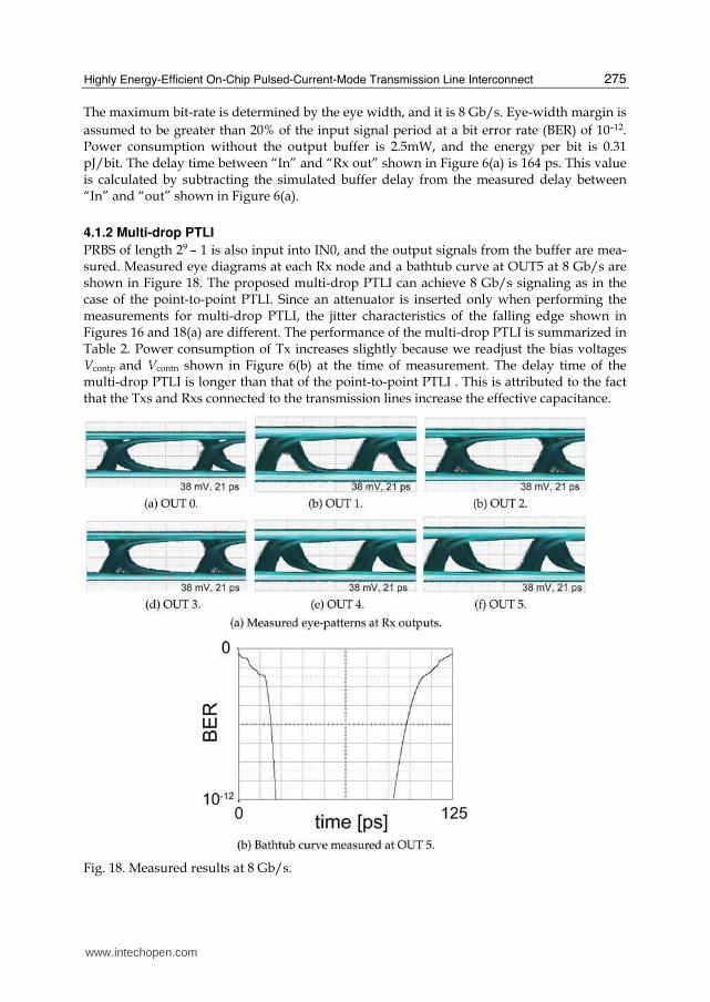
4.2 Discussions First, let us compare our interconnects with the conventional on-chip transmission line inter- connects (TLIs). As has been discussed in Section 1, the CML (current-mode logic) or LVDS (low-voltage differential signaling) amplifiers shown in Figure 19 are commonly used in conventional TLIs as Tx or Rx. The power consumption of the conventional TLIs does not depend on bit-rate, while that of the proposed PTLI reduces as the bit-rate reduces. This enables low-power operation and improves power efficiency, especially at low frequencies, as shown in Figure 20. The number of signal transitions decreases as bit-rate reduces; this is similar to the decrease in the activity factor. Hence, it is expected that as the activity factor decreases, the proposed PTLI has lesser energy per bit than the conventional TLIs. The proposed PTLI would be useful in improving the bandwidth and power efficiency of on-chip networks whose activity factors and bit-rates are changed frequently.
Fig. 19. CML and LVDS amplifiers that are commonly used as Tx or Rx.
www.intechopen.com
Highly Energy-Efficient On-Chip Pulsed-Current-Mode Transmission Line Interconnect
277
Fig. 20. Bit-rate dependence of power and energy per bit.
Fig. 21. Performance comparisons.
www.intechopen.com

Solid State Circuits Technologies
278
Now, comparisons with other interconnects are discussed here. We compare the proposed PTLI with the conventional on-chip interconnects such as RC lines, optical interconnections, and TLIs. Comparison of the delay time and energy per bit are shown in Figure 21(a). Smaller delay and smaller energy per bit mean better performance. In order to compare the delay and power consumption of these interconnects for a uniform line length of 1 cm, we recalculate the values under the following conditions:
• Repeater-less interconnects: The delay time of the interconnect is the sum of that of Tx,
on-chip wire, and Rx. A relative permittivity εr of 4 is assumed, and the delay of the transmission line is 6.7 ps/mm. Power consumption is assumed to be determined by Tx and Rx and does not depend on line lengths.
• Repeater-inserted interconnects: Delay and power consumption are proportional to line length.
• Delay of interconnect (Lee et al., 2004): Wire latency of 320 ps/5mm is reported in this paper, and delay of 640 ps is used for wiring portion.
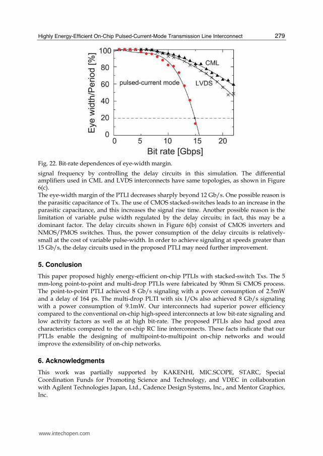
The delay time of the proposed PTLIs and the other TLIs are almost equal. This indicates that the delay characteristics of the proposed PTLIs are better than those of other on-chip interconnects. Energy per bit of our interconnects is almost the same as that reported in a previous study (Ito et al., 2008) and is greater than that reported in another study (Ito et al., 2007). The operating frequency in the previous study (Ito et al., 2007) is higher than that of the proposed PTLI. However, the comparison of the power consumption at 8 Gb/s shows that the power consumption of PTLI is smaller than that in (Ito et al., 2007), as shown in Figure 20. Wiring area is one of the most significant characteristics of on-chip interconnects. Since transmission lines usually occupy large area, on-chip TLIs are required to achieve better area per bit compared to the other on-chip interconnects. Energy per bit and area per bit of the on-chip high-speed interconnects are shown in Figure 21(b). Small energy per bit and small area per bit indicate good performance. The area occupied by the differential transmission line is assumed to be (line width) × 2 + (space between lines) × 3 and that occupied by single-ended RC line is (line width)×3. On-chip interconnects using RC lines have better characteristics in terms of area per bit than TLIs; this is because of the fine line width of the RC lines. However, the maximum bit-rate of RC interconnects is lesser than that of TLIs. Maximum bit-rate comparable to that of TLIs can be achieved by using RC lines in a bundle; however, this would imply that the RC lines will occupy virtually the same area as the TLIs. The area per bit of the proposed point-to-point PTLI is almost equal to that of the other point-to-point TLIs (Gomi et al., 2004; Ito et al., 2005; Ishii et al., 2006; Ito et al., 2007, 2008; Lee et al., 2004). The area per bit of the proposed multi-drop PTLI is the equal to the bidirectional and multi-drop transmission line interconnects (Ito et al., 2008). Thus, the proposed PTLIs are comparable to other on-chip TLIs in view of area and bit-rate. Finally, we shall discuss the capability of the proposed PTLI. Although the measured maximum bit-rate is 8 Gb/s, this limitation may be overcome by the proposed PTLI if better buffers are used for measurement. In order to simplify the discussion, we do not consider buffers in the following. Figure 22 shows the simulation result of the dependence of eye-width margin on signal bit-
rate at a bit error rate of 10–12. The eye diagram is observed at “Rx out” in Figure 6(a). The pulse width of the proposed PTLI is optimized to have the minimum pulse-width for each
www.intechopen.com
Highly Energy-Efficient On-Chip Pulsed-Current-Mode Transmission Line Interconnect
279
Fig. 22. Bit-rate dependences of eye-width margin.
signal frequency by controlling the delay circuits in this simulation. The differential amplifiers used in CML and LVDS interconnects have same topologies, as shown in Figure 6(c). The eye-width margin of the PTLI decreases sharply beyond 12 Gb/s. One possible reason is the parasitic capacitance of Tx. The use of CMOS stacked-switches leads to an increase in the parasitic capacitance, and this increases the signal rise time. Another possible reason is the limitation of variable pulse width regulated by the delay circuits; in fact, this may be a dominant factor. The delay circuits shown in Figure 6(b) consist of CMOS inverters and NMOS/PMOS switches. Thus, the power consumption of the delay circuits is relatively- small at the cost of variable pulse-width. In order to achieve signaling at speeds greater than 15 Gb/s, the delay circuits used in the proposed PTLI may need further improvement.
5. Conclusion
This paper proposed highly energy-efficient on-chip PTLIs with stacked-switch Txs. The 5 mm-long point-to-point and multi-drop PTLIs were fabricated by 90nm Si CMOS process. The point-to-point PTLI achieved 8 Gb/s signaling with a power consumption of 2.5mW and a delay of 164 ps. The multi-drop PLTI with six I/Os also achieved 8 Gb/s signaling with a power consumption of 9.1mW. Our interconnects had superior power efficiency compared to the conventional on-chip high-speed interconnects at low bit-rate signaling and low activity factors as well as at high bit-rate. The proposed PTLIs also had good area characteristics compared to the on-chip RC line interconnects. These facts indicate that our PTLIs enable the designing of multipoint-to-multipoint on-chip networks and would improve the extensibility of on-chip networks.
6. Acknowledgments
This work was partially supported by KAKENHI, MIC.SCOPE, STARC, Special Coordination Funds for Promoting Science and Technology, and VDEC in collaboration with Agilent Technologies Japan, Ltd., Cadence Design Systems, Inc., and Mentor Graphics, Inc.
www.intechopen.com

Solid State Circuits Technologies
280
7. References
Bakoglu, H. B., Circuits, Interconnections, and Packaging for VLSI, AddisonWesley, 1990. Bashirullah, R.,Wentai, L., Cavin, R., and Edwards, D. (2004). A 16 Gb/s adaptive
bandwidth on-chip bus based on hybrid current/voltage mode signaling, IEEE Symposium on VLSI Circuits, Digest of Technical Papers, pp. 392-393.
Chang, R. T., Talwalkar, N., Yue, C. P., and Wong, S. S. (2003). Near speed-of-light signaling over on-chip electrical interconnects, IEEE Journal of Solid-State Circuits, vol. 38, no. 5, pp. 834–838.
Gomi, S., Nakamura, K., Ito, H., Okada, K., and Masu, K. (2004). Differential transmission line interconnect for high speed and low power global wiring, IEEE Custom Integrated Circuits Conference, pp. 325–328.
Ishii, T., Ito, H., Kimura, M., Okada, K., and Masu, K. (2006). A 6.5-mW 5-Gbps on-chip differential transmission line interconnect with a low-latency asymmetric Tx in a 180nm CMOS technology, IEEE Asian Solid-State Circuits Conference, pp. 131–134.
Ismail, Y. I., Friedman, E. G., and Neves, J. L. (1998). Figures of merit to characterize the importance of on-chip inductance, ACM/IEEE Design Automation Conference, pp. 560– 565.
Ito, H., Inoue, J., Gomi, S., Sugita,H., Okada, K., and Masu, K. (2004). On-chip transmission line for long global interconnects, IEEE International Electron Devices Meeting, pp. 677–680.
Ito, H., Sugita, H., Okada, K. and Masu, K. (2005). 4 Gbps on-chip interconnection using differential transmission line, IEEE Asian Solid-State Circuits Conference, pp. 417–420.
Ito, H., Seita, J., Ishii, T., Sugita, H., Okada, K., and Masu, K. (2007). A low-latency and high-power-efficient on-chip LVDS transmission line interconnect for a RC interconnect alternative, IEEE International Interconnect Technology Conference, pp. 193-195.
Ito, H., Kimura, M., Miyashita, K., Ishii, T., Okada, K., and Masu, K. (2008). A bidirectional-and multi-drop-transmission-line interconnect for multipoint-to-multipoint on-chip communications, IEEE Journal of Solid-State Circuits, vol. 43, no. 4. pp. 1020–1029.
Jose, A. P., Patounakis G., and Shepard, K. L. (2006). Pulsed current-mode signaling for nearly speed-of-light intrachip communication, IEEE Journal of Solid-State Circuits, vol. 41, no. 4, pp. 772–780.
Kyriakis-Bitzaros, E. D., Haralabidis, N., Lagada,M., Georgakilas, A., Moisiadis, Y., and Halkias, G. (2001). Realistic end-to-end simulation of the optoelectronic links and comparison with the electrical interconnections for system-on-chip applications, Journal of Lightwave Technology, vol. 19, no. 10, pp. 1532-1542.
Lee, K., Lee, S., Kim, S., Choi, H., Kim, S., Lee, M. W., and Yoo, H.-J. (2004). A 51mW 1.6GHz on-chip network for low-power heterogeneous SoC platform, IEEE International Solid-State Circuits Conference Digest of Technical Papers, 2004, pp. 152-153.
Lee, K., Lee, S., and Yoo, H.-J. (2006). Low-power network-on-chip for high performance SoC design, IEEE Transaction on Very Large Scale Integrated Systems, vol. 14, no. 2, pp. 148-160
Schinkel, D., Mensink, E., Klumperink, A. M., Tuijl van, Ed (A.J.M.), and Nauta, B. (2006). A 3-Gb/s/ch transceiver for 10-mm uninterrupted RC-limited global on-chip Interconnects, IEEE Journal of Solid-State Circuits, vol. 41, no. 1, pp. 297-306
www.intechopen.com

Solid State Circuits TechnologiesEdited by Jacobus W. Swart
ISBN 978-953-307-045-2Hard cover, 462 pagesPublisher InTechPublished online 01, January, 2010Published in print edition January, 2010
InTech EuropeUniversity Campus STeP Ri Slavka Krautzeka 83/A 51000 Rijeka, Croatia Phone: +385 (51) 770 447 Fax: +385 (51) 686 166
InTech ChinaUnit 405, Office Block, Hotel Equatorial Shanghai No.65, Yan An Road (West), Shanghai, 200040, China
Phone: +86-21-62489820 Fax: +86-21-62489821
The evolution of solid-state circuit technology has a long history within a relatively short period of time. Thistechnology has lead to the modern information society that connects us and tools, a large market, and manytypes of products and applications. The solid-state circuit technology continuously evolves via breakthroughsand improvements every year. This book is devoted to review and present novel approaches for some of themain issues involved in this exciting and vigorous technology. The book is composed of 22 chapters, written byauthors coming from 30 different institutions located in 12 different countries throughout the Americas, Asiaand Europe. Thus, reflecting the wide international contribution to the book. The broad range of subjectspresented in the book offers a general overview of the main issues in modern solid-state circuit technology.Furthermore, the book offers an in depth analysis on specific subjects for specialists. We believe the book is ofgreat scientific and educational value for many readers. I am profoundly indebted to the support provided byall of those involved in the work. First and foremost I would like to acknowledge and thank the authors whoworked hard and generously agreed to share their results and knowledge. Second I would like to express mygratitude to the Intech team that invited me to edit the book and give me their full support and a fruitfulexperience while working together to combine this book.
How to referenceIn order to correctly reference this scholarly work, feel free to copy and paste the following:
Tomoaki Maekawa, Shuhei Amakawa, Hiroyuki Ito, Noboru Ishihara, and Kazuya Masu (2010). Highly Energy-Efficient On-Chip Pulsed-Current-Mode Transmission Line Interconnect, Solid State Circuits Technologies,Jacobus W. Swart (Ed.), ISBN: 978-953-307-045-2, InTech, Available from:http://www.intechopen.com/books/solid-state-circuits-technologies/highly-energy-efficient-on-chip-pulsed-current-mode-transmission-line-interconnect
www.intechopen.com

www.intechopen.com

© 2010 The Author(s). Licensee IntechOpen. This chapter is distributedunder the terms of the Creative Commons Attribution-NonCommercial-ShareAlike-3.0 License, which permits use, distribution and reproduction fornon-commercial purposes, provided the original is properly cited andderivative works building on this content are distributed under the samelicense.
Related Documents