High-Voltage High Slew-Rate MOSFET Op-Amp Design 2005 Engineering Design Expo University of Idaho Erik J. Mentze Jennifer E. Phillips April 29, 2005 Project Sponsor: Apex Microtechnology Advisors: Dave Cox, Herbert Hess

High-Voltage High Slew-Rate MOSFET Op-Amp Design 2005 Engineering Design Expo University of Idaho Erik J. Mentze Jennifer E. Phillips April 29, 2005 Project.
Dec 22, 2015
Welcome message from author
This document is posted to help you gain knowledge. Please leave a comment to let me know what you think about it! Share it to your friends and learn new things together.
Transcript
High-Voltage High Slew-Rate MOSFET Op-Amp Design
2005 Engineering Design ExpoUniversity of Idaho
Erik J. MentzeJennifer E. Phillips
April 29, 2005
Project Sponsor:Apex Microtechnology
Advisors:Dave Cox, Herbert Hess
Overview
→ Project Description→ Design Methodology→ Theory of Operation→ Implementation and Results→ Conclusions and Future Work
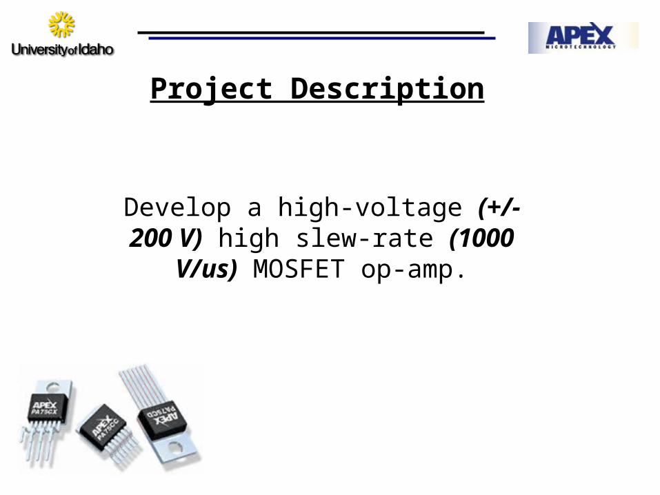
Project Description
Develop a high-voltage (+/- 200 V) high slew-rate (1000 V/us)
MOSFET op-amp.
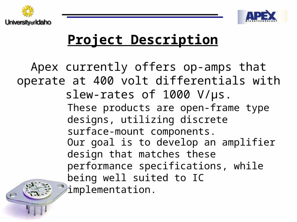
Apex currently offers op-amps that operate at 400 volt differentials with slew-rates of 1000 V/μs.
These products are open-frame type designs, utilizing discrete surface-mount components.
Our goal is to develop an amplifier design that matches these performance specifications, while being well suited to IC implementation.
Project Description
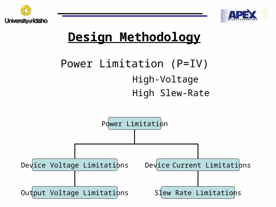
Design Methodology
Power Limitation
Device Voltage Limitations Device Current Limitations
Slew Rate LimitationsOutput Voltage Limitations
Power Limitation (P=IV)
High-Voltage
High Slew-Rate
General Amplifier Topologies• Find topology candidates• Throw out those that are obviously deficient• Analytically compare the “finalists” to make the
best choice
Hardware Implementation• Find components that meet our design
requirements• Adapt chosen topology to meet physical
requirements• Simulate Implementation• Attempt to Implement Design
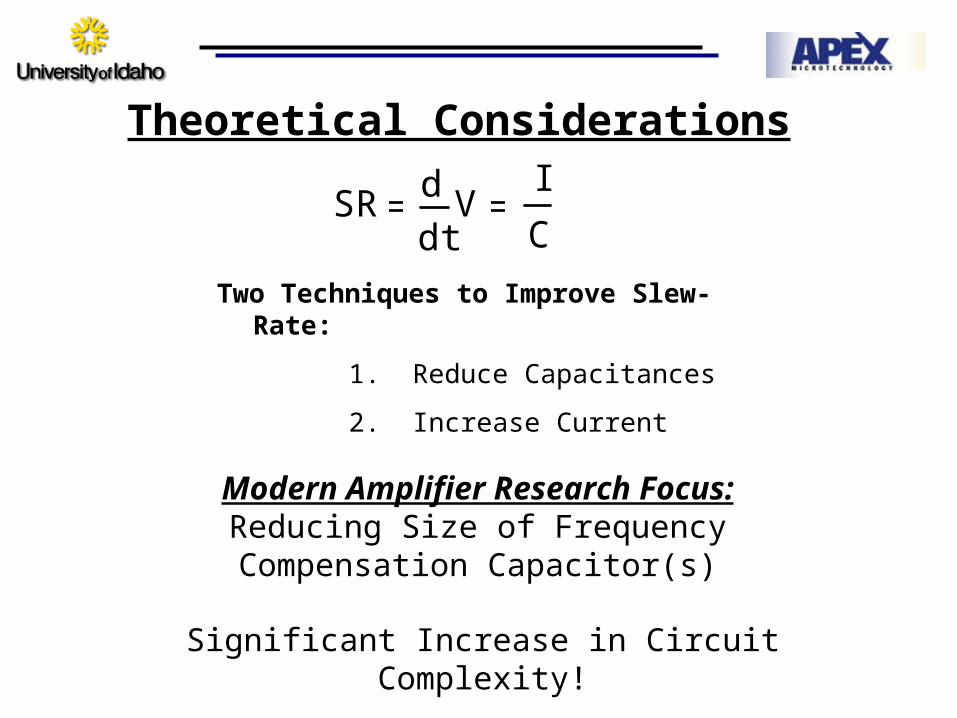
SRtVd
d
I
C
Significant Increase in Circuit Complexity!
Theoretical Considerations
Modern Amplifier Research Focus:Reducing Size of FrequencyCompensation Capacitor(s)
Two Techniques to Improve Slew-Rate:
1. Reduce Capacitances
2. Increase Current
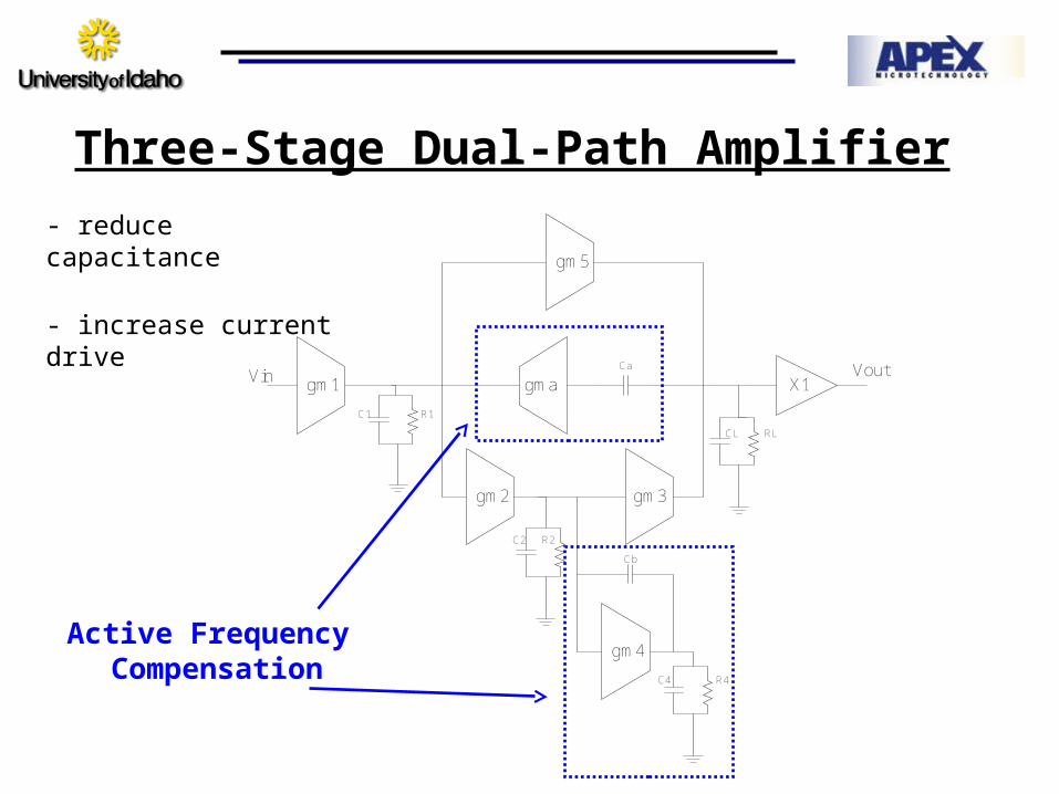
gm1
gm2
gma
gm4
gm5
X1
gm3
C1
Ca
Cb
R1
C2 R2
C4 R4
CL RL
VoutVin
Active Frequency Compensation
Three-Stage Dual-Path Amplifier
- reduce capacitance
- increase current drive
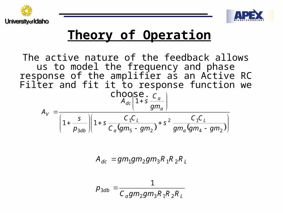
Theory of Operation
The active nature of the feedback allows us to model the frequency and phase response of the amplifier as an
Active RC Filter and fit it to response function we choose.
24
12
25
1
3
11
1
gmgmgm
CCs
gmgmC
CCs
p
s
gm
CsA
A
a
L
a
L
db
a
adc
V
Ldc RRRgmgmgmA 21321
Ladb RRRgmgmC
p2132
31
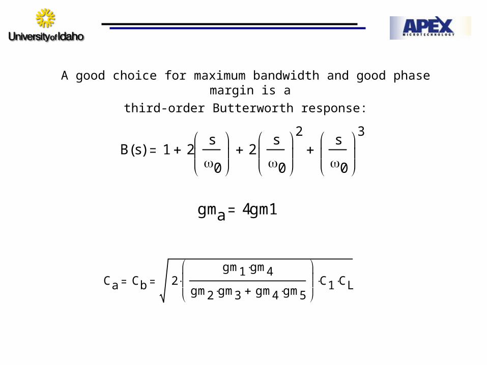
A good choice for maximum bandwidth and good phase margin is a
third-order Butterworth response:
B s( ) 1 2s
0
2s
0
2
s
0
3
gma 4gm1
Ca Cb 2gm1 gm4
gm2 gm3 gm4 gm5
C1 CL
Implementation
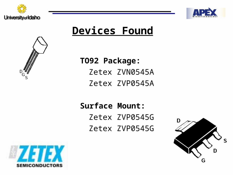
Devices Found
TO92 Package:
Zetex ZVN0545A
Zetex ZVP0545A
Surface Mount:
Zetex ZVP0545G
Zetex ZVP0545G
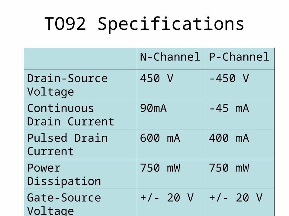
TO92 Specifications
N-Channel P-Channel
Drain-Source Voltage
450 V -450 V
Continuous Drain Current
90mA -45 mA
Pulsed Drain Current 600 mA 400 mA
Power Dissipation 750 mW 750 mW
Gate-Source Voltage +/- 20 V +/- 20 V
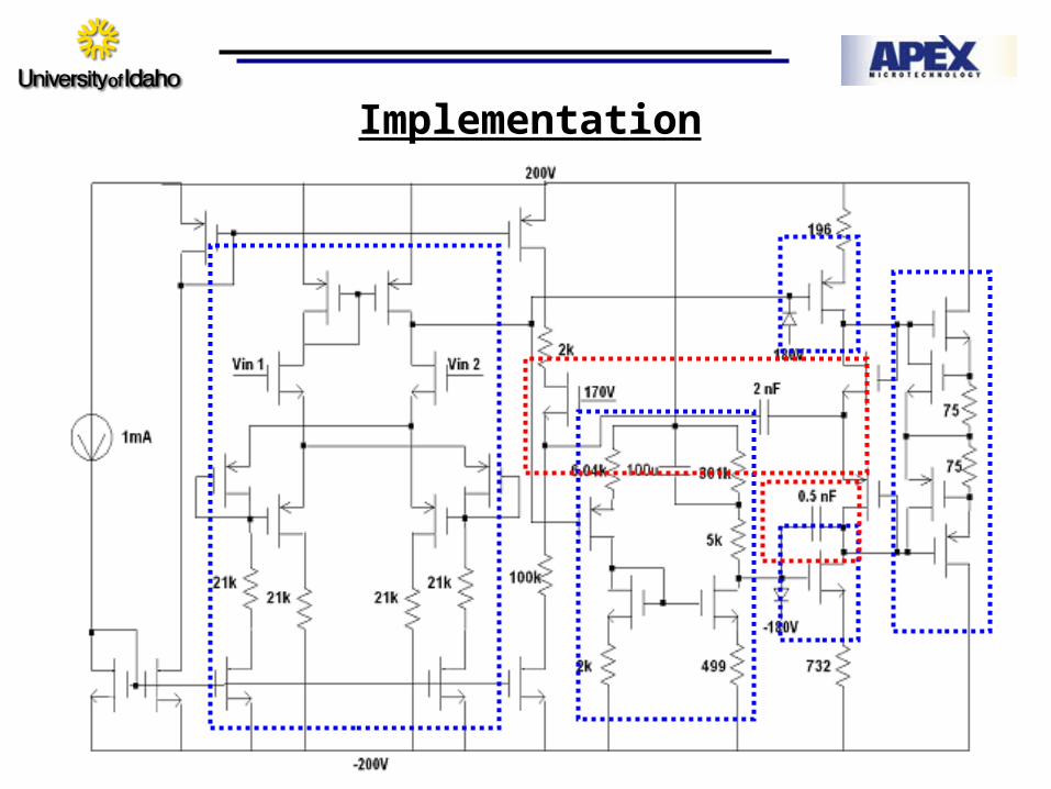
Implementation
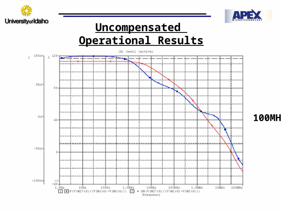
Uncompensated Operational Results
DC Gain: 110dB
Unity Gain Freq: 100MHz
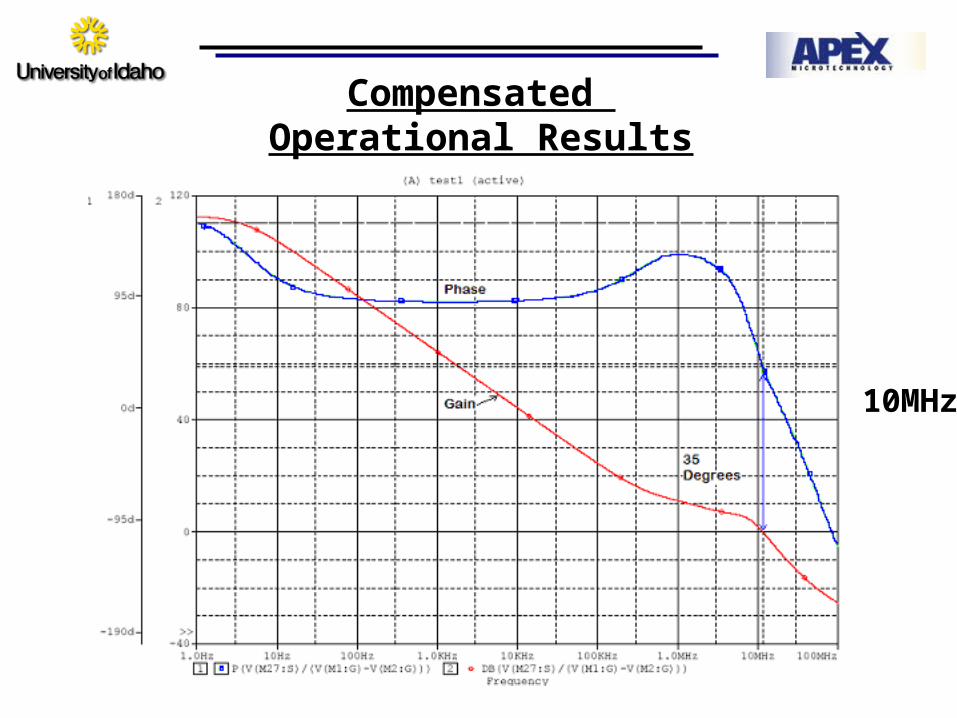
Compensated Operational Results
DC Gain: 110dB
Unity Gain Freq: 10MHz
Phase Margin: 35o
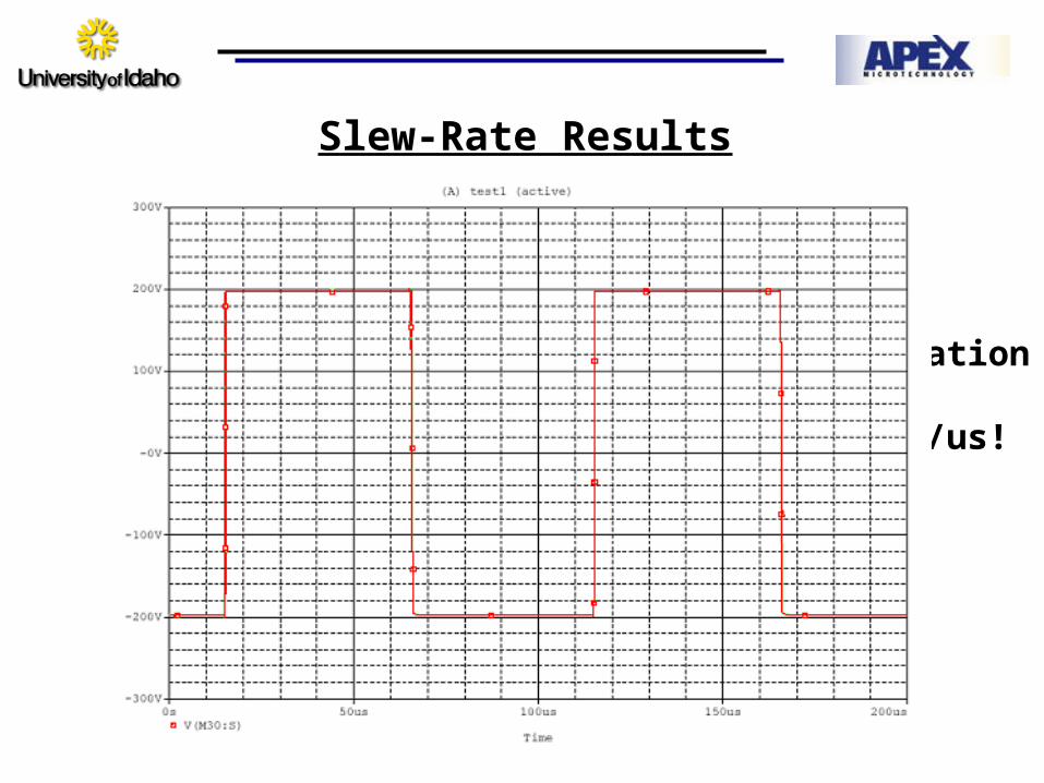
Slew-Rate Results
Rail-to-Rail Operation
Slew-Rate: 2000 V/us!
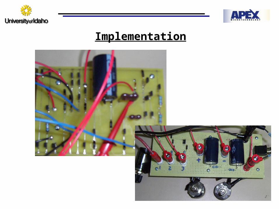
Implementation
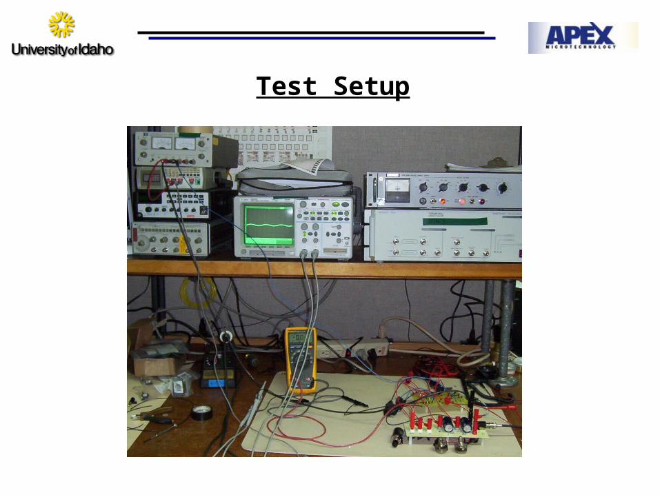
Test Setup
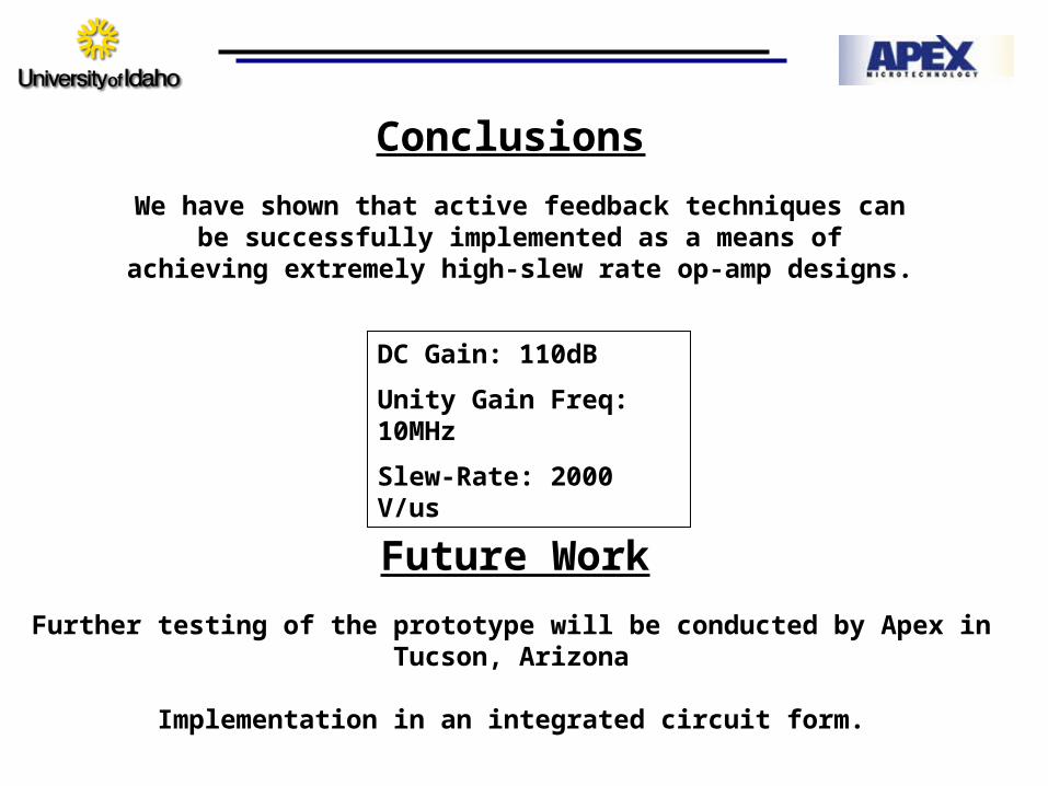
Conclusions
We have shown that active feedback techniques can be successfully implemented as a means of achieving extremely
high-slew rate op-amp designs.
DC Gain: 110dB
Unity Gain Freq: 10MHz
Slew-Rate: 2000 V/us
Further testing of the prototype will be conducted by Apex in Tucson, Arizona
Implementation in an integrated circuit form.
Future Work
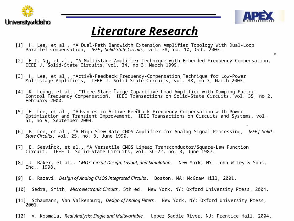
Literature Research[1] H. Lee, et al., “A Dual-Path Bandwidth Extension Amplifier Topology With Dual-Loop Parallel Compensation,” IEEE
J. Solid-State Circuits, vol. 38, no. 10, Oct. 2003.
[2] H.T. Ng, et al., “A Multistage Amplifier Technique with Embedded Frequency Compensation,” IEEE J. Solid-State Circuits, vol. 34, no 3, March 1999.
[3] H. Lee, et al., “Active-Feedback Frequency-Compensation Technique for Low-Power Multistage Amplifiers,” IEEE J. Solid-State Circuits, vol. 38, no 3, March 2003.
[4] K. Leung, et al., “Three-Stage Large Capacitive Load Amplifier with Damping-Factor-Control Frequency Compensation,” IEEE Transactions on Solid-State Circuits, vol. 35, no 2, February 2000.
[5] H. Lee, et al., “Advances in Active-Feedback Frequency Compensation with Power Optimization and Transient Improvement,” IEEE Transactions on Circuits and Systems, vol. 51, no 9, September 2004.
[6] B. Lee, et al., “A High Slew-Rate CMOS Amplifier for Analog Signal Processing,” IEEE J. Solid-State Circuits, vol. 25, no. 3, June 1990.
[7] E. Seevinck, et al., “A Versatile CMOS Linear Transconductor/Square-Law Function Circuit,” IEEE J. Solid-State Circuits, vol. SC-22, no. 3, June 1987.
[8] J. Baker, et al., CMOS: Circuit Design, Layout, and Simulation. New York, NY: John Wiley & Sons, Inc., 1998.
[9] B. Razavi, Design of Analog CMOS Integrated Circuits. Boston, MA: McGraw Hill, 2001.
[10] Sedra, Smith, Microelectronic Circuits, 5th ed. New York, NY: Oxford University Press, 2004.
[11] Schaumann, Van Valkenburg, Design of Analog Filters. New York, NY: Oxford University Press, 2001.
[12] V. Kosmala, Real Analysis: Single and Multivariable. Upper Saddle River, NJ: Prentice Hall, 2004.
Related Documents