PROCEEDINGS OF THE CONFERENCE ON HIGH-TEMPERATURE ELECTRONICS March 25-27, 1981 Tucson, Arizona SPONSORED BY IEEE Industrial Electronics and Control Instrumentation Group iEEE Solid State Circuits Council NASA National Aeronautics and Space Administration Department of Energy Division of Engineering, Mathematics, and Geoseiences Nuclear Regulatory Commission Division of Reactor Safety Research National Science Foundation Los Alamos National Laboratory The University of Arizona r«| S "CHI658-4

Welcome message from author
This document is posted to help you gain knowledge. Please leave a comment to let me know what you think about it! Share it to your friends and learn new things together.
Transcript
PROCEEDINGSOF THE CONFERENCE ON
HIGH-TEMPERATURE ELECTRONICSMarch 25-27, 1981
Tucson, Arizona
SPONSORED BY
IEEE Industrial Electronics and ControlInstrumentation Group
iEEE Solid State Circuits Council
NASA National Aeronautics and Space Administration
Department of EnergyDivision of Engineering, Mathematics, and Geoseiences
Nuclear Regulatory CommissionDivision of Reactor Safety Research
National Science Foundation
Los Alamos National Laboratory
The University of Arizona
r«|S
"CHI658-4
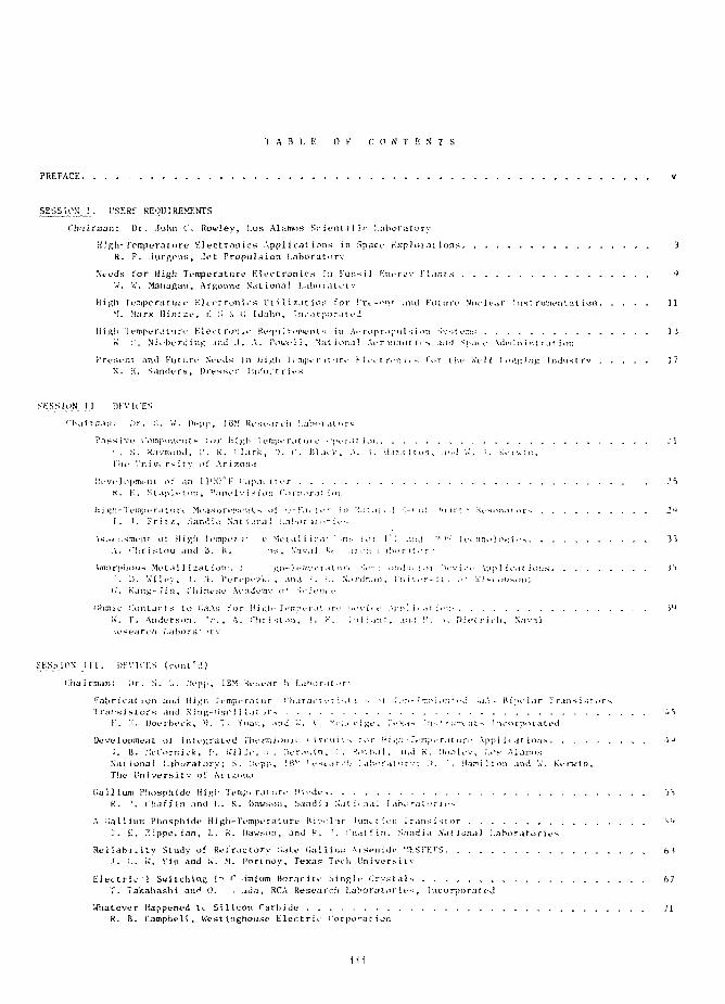
T A B U : O F C O N T E N T S
PREFACE.
SESSION' ! , USERS-' REQUIREMENTS
Ch'iirmnnz i)r , John C, Rowley, Los Alamos Sr i en t i f i r l a b o r a t o r y
High-Temper a Lure F l e c t r o n i c s Appl i ca t ions in Space Expl 01 ai i uns 3R. F. . lurRcns, lot P ropu l s ion I .ahoraturv
Needs fo r High Tempera l u r e E lec t ron ios :;i Fos s i l Kneriz.v Pl.int.s , l)V . V . M a n a f i a n , A r g o n n o N a t i o n a l K a h o r a t i , r v
H i Rh T e m p e r a t u i e E K - r t r o n i i s V t i 1 i z.-it i o n t o r P r t ^*"»T a n d F u t u r e Nuc J i- . i r 1 n s t r u m e n t a t i o n 11M. Ma r x H i n t ; : e , H ^ i (i I d a h o , I iii" n r j i o r . i t e d
Hi g h I e m p e r . i t l i r e E l e c t r o n <i- R e q ' i I r i - m u n t K i n At- r o p r ^ p n l s i o n v : s t e r r s 1 iU'. ( ' . N i e b e r t J i n g a n d J . A . !Vv<-} I , N a t i o n a l A e r m.-ni t i c s . J D J ^ p a i - e \ i i n l n i s i r a t i o n
P r e s e n t a n d F u t u r e Need? ; in H i ^ l i l \ -nipe r i t -tr*.- H < ' r i r o n u - s f o r t fie V e i l l o i ^ i n g I n d u s i r v 17X . H. S a n d e r s , D r e s s e : ' I n d u . t r i e s
S K S S h t N I I - OKVICES
T h a i nr i . i [ t : !)r . S , W . D e p p , I BM R t - s e a r r h ! , a h o i a i ' -> rv
P a s s i v e roff i |kHK'!U,s l o r Hi>;h I f r apc r a t un . - . " [ v r . i r i n n ^1I . S . R. ' tvmiJiiJ , H. K. ' " l a r k , !>. i \ B l a v k , '.">. i . il .i?.i U o n , .!•)•• V.'. ' . Ket w i n .T h e t ' n i v e r ^ i t v o f A r i z o n . i
! : . ' v e l o p n i t - n i . o f a n H O O T dp.i^ i i o r
K . K . S t . ip U- t o n , r . i n e I v i s i\>ti r . i r p o r . i : icni
Hi ^ h - T e m p t - r a t u r v M t - a s u r i ' i r ^ - n t -, of •.)- r . i r t i v i n '•.'.;! a : t A - ' . - ( t i t H i a r r .* H t ^ o n . n «>r-.
I . 1. F r i i z , S n n d i * i N a t i . m a 1 ! . l i ! n » r , u i " ' i i i ~ >
\ s . - . r . s s ; n f i U o ! fi t ^ h i ' e m p e r )* e >U't a I I i ; ' a* n s r or I' \ .\:\<.\ M '1 '- [\-( n n i ' l i>*; j --s.\ . CIi r i s t f i u i int i &• K . \^ t NViv.j J }W- . i r i i i i a i m r . i f . < > r .-
A m o r p h o u s M e t a I I 1 z a t i o n . t K'»" - t - ^ p i - r . u ' i v . S. - r- : mi . i i ! . : . i r : i c v j .-*- \ p p 1 i V a t i o r ;
'• . 0 . Wi 1 e y , .F. J i . ? e r t - p e ? k i , a n d ! . f.". N<>rdr].<n , Cn i v r r - . : I v .- r V i s c n i s i i n ;(.". K . i n ^ - . J i n , ('Ji i n e s e A e a d e r a v nf ••;<- i e m -•
t>hmic C o n t a c t s t o (i.-jAs f o r !) i i ;h- l'i 'ir.pt- r.v. m - ->ovit<.- . % p r > 1 i . a t I-*::-
W. T . ' \nijt1 r s c n . T r . , A . I ' ^ i r i s t n u , !. K . i i •; ] j a n : , . K I . I '.'., :•., Di f t r i r J i , Xa v i l
SESSION' I I I . OKVU'ES ( c o n t ' d )
C h a i r n u i n : i > r . S . ; . . H e p p , IBM i i e ^ t - a r h L a h o r . J t o r v
F a h r i c a t i o n ;tiu\ )\ i g h T f r n p t - r a : u r I ' h a r n r i k T i s t i . -- >M !, ' - . - f ; M . )n f •• d • ia.'. - R i p o l <ir 1" r . t n s i ^ t o r sT r a n s i s t o r s a n d K i n g - ( ) s i % i 1 l a I ( r s
F . 'A . [Joe r b e r k t H . T . Y n a r . , a n d •-.', V . Sc.'.t \' i >;e , I *•>;.!;- I n-• ' r t i - \ ; i t -i I n r o r p o C i t e d
ve lop raen t of I n t e g r a t e d Themii>n n *' i n%\i i i •-» r or" H i i;h • 7crii'«-ra[ uri- App I i c a t ion-sI. B. Mi'C'onniok. ['. U ' i l d c , i . ' . V r o u i n , i . ' - lovhal . And K. f ino tev , :.t»s A I J D O SNat i o n a l L a b o r a t o r y ; S. ' .Vpp, ' Hv' ' ' t -^ra ri 'h L a h ^ r a t or- - ; ;>. ' . ;j.ini 11 on and V. K^rwi n .The Vn i v e r s i t v o i Ar i '/A.ua
D a l l i u m P h o s p h i d e H i g h T e n i p . r a i u r t - ! M t i d ^ - - . j SK . I , C)isi f i n a n d 1.. H . ( l a w s o n , S a n d i i N'at i . : i a l I a t v - a : <»ri c s
A C a l l l i m P h o s p h i d e H i g h - T e m p e r a t u r e H i p n l - i r ! u i u t i o n I r j n s i m o r
T - E . 7. : p p e » t a n , L . R. D a w s o n , a n d f*'. ' . : ' u a l f i n . S a n d i a Na t i on,i 1 J . - i h o r a t o r i t - s
S t ' l i a h i . i t y S t u d y o( R e f r a c t o r y t i a t e C a l l i u n i A r s e n i d e MhSKETS MJ . i... W. Y i n a n d U*. M. P o r t n o y , T e x a s Te* h U n i v e r s i t v
E l e c t r i c ' 1 S w i t c h i n g ir- c dmi t im B o r a c i t e S i n g l e f ^ r y s t a l . s hi
T. T a k a h a s M an^ 0. . j d a , RCA R e s e a r c h l.<ihor.-itor i e s r I n c o r p o r a t e d
Wi ia tever Happened t i S i l i c o n C a r b i d e 71R. B. CnmpbelL, West i n g h o u s e E l e c t r i i *'orpo*-.n ion
SESSION IV. CIRCUITS AND SYSTEMS
Chairman: Jim Moyer, National Semiconductor Corporation
-55 to +2Q0°C 12 Bit Analog-to-Digital Converter 77
L. R. Smith and P. K. Prazak, Burr-Brown Research Corporation
Process Characteristics and Design Methods for a 300° QUAD OP AMP 81J. D. Bcasom and R. B. Patterson, III", Harris Semiconductor
Hybrid A/I) Converter for 200cC Operation 35
M. R. Sullivan and J. B. Toth, Micro Networks Company
Wi reless, In-Vessel Neutron Mon itor for Initial Core-Loading of Advanced Breeder Reactors. . . . 89
.1. T. De Lorenzo, M. M. Chiles, J. M. Rochelle, and K. H. Valentine, Oak Ridge
Nat Lonal Laboratory; T. V. Blalock and E. -I. Kennedy, I'niversity of Tennessee
Solid State Microelect ronics Tolerant to Rad iat ion and H igh Temperature 93
B. I.. Draper and D. W. Palmer, Sandia National Laboratories
High i'emperature LSI 97
D. C. Den ing, L. J . Raj^onese, and C. Y, Lee, C.uncral Electr ic electronics Laboratory
'1 i j/,h~Tempurature Complementary Meta 1 Oxide Semiconductors (CMOS) 101I. n. Mc-Brnyer, Sandia Nat ionnl Laboratories
SKS_S_in_N _V . PACKAl: I Nt;
Chai m a n : W. S . R e a d , J e t P r o p u l s i on L a b o r a t o r y
A P r e s e n t l y A v a i l a b l e ICnergy S u p p l y f o r High Ti -mpera i a r e E n v i r o n m e n t ( 5 5 0 - 1 0 0 0 ° F) 107.1 . .JarcjueJ in a n d H. L. V i c , l.;ibnr;itoi res de Mar<-otis*sis
St uf i 'fd Mo Lave r a s a I>i f i u s i o n l iar r i c r in Met a 11 i z a t i o n s f o r Hi p,h Tempo r a L u r e E l e c t r o n i c s . . . I l lJ . K. Boa 11, V . R u s s e l I , ami D . P . Srai t h , i- t-ni-ral Kl i -c t r i c Cumpany
R t - f r a i - t o r v C l a s s and l U a s ^ C e r a m i c Tube S e a l s 115>..'. V . i>a 11 a r J jnd I). L . S t e w a r t , Sand i a Nat ion.nl L a b o r a t o r i e s
P a c k a ^ i ny, I 'eehn i r jues i o r Low-Al t i t i i d e Venus Bal l o o n Beacon 117T. !. Kord.-n a n d . 1 . V.. U ' i n s l o w , Jet . P r o p u l s i o n L a b n r . j t n r y
H i^h T e m p e r a t u r e \Al. ,0 ^) I n s u l a t i o n and I. i &}\l We ighL C o n d u c t o r s 12 3H. V.'a 1 k e r , Pe rma l u s t e r , I n c o r p o r a t e d
SESSION V I . S P K C I ' L KKYNOn-: ADDRKSS
!'r . k o b i - r t P rv , liuu Id , I m o r p n r a i i - i l
A ( o n l e r e n c e P e r s p e t t i v r
I'REFACE
J. Byron McCormick, Conference ChairmanLos Alamos National Laboratory
Major impetus for the development of high tempera-ture electronic materials, devices, circuits and sys-tems can probably be credited to the energy crisiswhich appeared dramatically in 1974. At that time itwas acknowledged that the necessary discovery and ex-ploitation of national energy resources would requirea long-term commitment to research and development, andfederal funds were made available for this purpose. In1975, a workshop was held to set directions for work ingeothermal exploration,1 and a number of contractswere subsequently negotiated. As work continued, inter-est broadened beyond the geothermal area. In 1978, Dr.A. F. Veneruso.of Sandia Laboratories, organized a ses-sion on High Temperature Electronics at Midcon 1978in Dallas, Texas.' This session included a paper onaircraft engine controls, as well as papers on integrat-ed circuits directed at the high-temperature needs ofthe well-logging industry. In 1979, interest broadenedstill further, as evidenced by the High TemperatureElectronics and Instrumentation Seminar organized inHouston, Texas by Dr. Veneruso. ' Most recentlv, a ses-sion of the 1980 Electro-Professional Program wss de-voted to The Frontiers of High Temperature Electronics'.'
More than five years have passed since the firstworkshop was held, and in that time much progre .s hasbeen made. Interest in the field has continuer to growand the diversity rf requirements has rapidly increased.It therefore seems important at this time to re-eval-uate the status of and directions for high temperatureelectronics research and development. This conferencehas been organized for that purpose. Specifically, theconference has three major objectives: to identifycommon needs among those in the user community; to putin perspective the directions for future work by focus-ing on the status of current research and developmentprograms; and to addrer , the problem of bringing topractical fruition the results of these efforts. Whilethe importance of the technical content of the papersis not to be underestimated, the Program Committee feltthat because of the diversity of interests representedin the audience, the identification of common problemsand the need for perspective with regard to the impli-cations, both technical and commercial, of these prob-lems were perhaps as important as the ht«h-tempera-ture technologies themselves. Accordingly, special at-tention was given to the program in two ways.
First, considerable care was taken to put togethera session on Users Requirements which included papersfrom as broad a spectrum as possible, and this sessionwas scheduled as the first of the conference. Second,the need for perspective was recognized to be parr ofthe broader problem of determining what results ol' re-search and development have long-range potential forcommercialization, and how these can be reduced to prac-tice. To meet this need we are introducing what we be-lieve to be an innovation in conferences of this type:the final session, A Conference Perspective, by Dr.Robert Pry, Vice-President for Research and Development,Gould, Inc. During the conference, Dr. Pry will talkwith as many as possible of the conference attendees.Combining the results of these encounters with what helearns of the status of the various high-temperaturetechnologies from the conference papers, he will devel-op a commentary of his views of the conference in gener-al, and technology transfer and commercialization inparticular. I would, therefore, encourage everyone who
has special needs in high-temperature electronics, oropinions about the field, to talk with Dr. Pry at sometime during the conference. I also hope that everyonewill plan to stay for this final and possibly mostimportant session.
It is worth noting that more than half the papersin the conference deal with materials and devices,rather than circuits and systems. While this is duein part to the conference emphasis on research and de-velopment, it is in larger measure a reflection of thelack of maturity of the field. Circuits and systemsare the last in the uevelopment chain of which materialform the beginning. The evolution to a mature technol-ogy base is unfortunately impeded by the relativelysmall size of the market for high temperature electron-ics when compared with, for example, the market command-ed by integrated circuit.5. This small size is not, how-ever, indicative of its importance when viewed in thecontext of national energy and spp-e programs. It is,therefore, the yoal of this conference to expedite thedevelopment of high temperature electronics for thesemost important applications.
No conference such as this cganized without the hard work oftive individuals; I wo lid like toserved on the Program Committee fcial acknowledgements are due Dr.Or. .Ian A. Narud, both of Los Alatory, for their outstanding and tt.iblis'i a program of the highestknowledpements are also due Dr. Chis staff in Special ProfessionalI'niversity of Arizona, for handliarrangements.
an be successfully or-a number of coopera-thank all those who
or their efforts. Spe-John C. Rowley andmos National Labora-
. efforts to es-qualitv. Special ac-. II. ilausenbauer andF.ducation at The
ng all the conference
Finally, I would like to express our gratitude tothose agencies which have contributed financially tothe success of the conference: The National Aeronau-tics and Space Administration; The Department of Energy,Division of Engineering, Mathematical and Geosciences;The Nuclear Regulatorv Commmission, Division of ReactorSaftev Research; and The National Science Foundation.
REFERENCES
L. E. Baker, et a1., Report of the GeophysicalMeasurements in neothermai Wells Workshop. Albu-querque, New Mexico, September 17-19, 1975.Sandia Report SAND 75-0608, Sandia National Labora-tory.
High Temperature Electronics, Session 21, 1978 Mid-ron Professional Program, Dallas, Texas, December12-14, 1978.
High Temperature Electronics and InstrumentationSeminar, Houston, Texas, December 3-4, 1979.
The Frontiers of High Temperature Electronics, Ses-sion 16, 1980 Electro-Professional Program, Boston,Massachusetts, May 13-15, 1980.
S E S S I O N I
U S E R S R E Q U I R E M E N T S
Cha i rrnan'
Dr. John C. RowleyI.os Alamos S c i e n t i f i c Labora toryI.os Alamos, New Mexi-o
HIGH TEMPERATURE ELECTRONICS APPLICATIONSIN SPACE EXPLORATIONS*
R.F. Jurgens
Jet Propulsion Laboratory4800 Oak Grove DrivePasadena, CA 91103
Electronic instruments and systems used for spaceexploration have not generally been exposed directly toharsh environments of outer space or the dense atmo-spheres of several of our planets. Instead, protectiveenclosures, insulation, shielding, and small heatingsystems are provided to control the environment. Alsothe design of spacecraft systems and instruments arecarried out with fairlv conservative design rules, be-cause the cost of a mission is high, and failure is easyto achieve. The design of electronic instruments foruse within the wide range of the earth's environment isdifficult enough, and extension of our electronic tech-nology to operate at very high or low temperatures orgreat pressures is no small challenge.
Operation of electronic systems in environmentshaving temperatures or pressures beyond the capabilityof the electronics requires systems to protect orinsulate the electronics i"rom the environment. Themaintenance ot the protection requires energy, andthe energy source itself may require protection. tnvacuous space, the energy transfer to the spacecraft isentirely dependent upon radiative transfer, and tempera-tures can be controlled by varying the reflectivity ofthe spacecraft surfaces. This form of control may re-quire l i t t l e energy since it often can be accomplishedwith l i t t l e more than the rotation of the spacecraft orthe reorientation of reflective panels. Pressure dif-ferences are seldom larger than the difference betweenLhat of the earth and vacuum. In these respects, theexploration of space is considerably les.s difficult thanthe exploration of the earth's inner space where tem-peratures and pressures are high.
The exploration of the planets having large atmo-spheres is entirely ;. different matte-. In the case ofVenus, for example, the surface temperature is near73O°K and the atmospheric pressure 90 bars. The atmo-spheric profiles of the large outer planets are relative-ly unknown, but one thing Is sure, both the pressure andtemperature will increase well beyond our technicalcapability to design instriiments before any surface islikely to be found. The depth to which these atmospherescan be studied depends on one of two things, 1. ourability to design probes that can withstand the greattemperatures and pressures, 2. the ability to transmitthe information through the dense absorbing atmospheres.
The problem of protecting electronic systems fromthe great temperatures and pressures of these atmospheresis a very different problem from that of outer space.Here the thermal energy transfer is caused primarily byconduction to the atmosphere. The atmospheric pressuresmay be hundreds of times greater than those of theearth's atmosphere, so our spacecraft may look more likea craft designed for deep ocean exploration. We havetwo choices as to the design of our craft, either wedesign our systems to withstand the high temperaturesand pressures, or we maintain temperature and pressuredifferences within the craft. The maintenance of tem-perature and pressure differences requires energy, andenergy is always a very expensive and a scarce commodityon any space probe. Therefore i t is very important thatwe minimize or eliminate the need to maintain such dif-
ferences. The extension of range of operating tempera-tures of electronic components and systems is a start inthat direction.
Missions
The exploration of the atmosphere of Venus willprobably be the first example of the use of high tem-perature electronic systems in space applications.Studies of the Venusian atmosphere could be accomplishedby the use of balloon borne instruments. The simplestsort of experiment might be one that determines onlythe circulation properties of the atmosphere at variousaltitudes. All that is required here is a beacon ofsufficient power to be tracked by either orbitingspacecrafts or from ground-based radio telescopes. Amore advanced probe might contain a radar transponder.The localization of the balloon, for example, could beaccomplished by VLBI, Doppler tracking, range trackingin the case of a transponder, and all combinations oftheye. Two missions are presently being studied. Thefirst carries only a simple beacon transmitter and flysat 18 km altitude where the temperature at about 325°C.Electronic breadboard designs for operation at thistemperature are presently being constructed and testedat IPL. The second flys between 40 and 48 km where thetemperature does not exceed 150°C. Here, more advancedinstrument packages are presently within the availabletechnology. Possible instruments include pressure,temperature, differential temperatures, light fluxes,lightning detectors, and sound pressure levels. Ballonmissions are likely to last no longer than a few daysto a few weeks, therefore only short term studies can becarried out (These are much longer, however, than thepresent Venera and Pioneer-Venus probes). Longermissions are desirable ard would most likely have to becarried out from the surface.
If a landing probe could sit on the highest partof Terra Ishtar (about 10 km above the mean surfacelevel) the temperature would be about 38O°C. A numberof interesting experiments could be accomplished fromthis remarkable peak including a l l the traditionalweather measurements, atmospheric turbulance, lightscattering from dust particles, and so on. Equally asinteresting are measurements related to planetary andsolar systems dynamics. For example, very accuratemeasurements of the rotation rate, direction of the spinaxis, and orbital motion could be made. These measure-ments could easily establish whether the rotation is insynchronous lock with the earth or if some form of pre-cession exists. As the planet rotates, two occultationscould be observed per revolution as viewed from theearth. An orbiting spacecraft could observe severaloccultations per day. Such measurements not only aidIn establishing the variation of the atmosphere butgive a measure of the turbulance which establishes theultimate "seeing" capability through the Venusian atmo-sphere at microwave frequencies.
Going to our outer planets, there Is much work tobe done. The f i rs t direct measuremnts of the Jovianatmosphere will be made by the Galileo space probes.These probes, like the PV probes, will lastashort timeuntil they are either crushed or their signal extin-guished by the absorption in the atmosphere. The data
they return will ultimately determine If other methodsof exploration are possible. Among the most exicitingmight be a hot air balloon mission to explore thecirculation below the visible c.'oud regions. Though itis too early to know what might be possible, high tem-perature electronics will most likely l.R required.
Going towards the inner part of our sriqr systemwe find Mercury and the Sun. The Mariner 1U spacecraftmeasured surface temperatures on Mercury ranging from90 to 460°K. Radiative transfer models indicate thattemperatures as high as 650°K (377°C) exist when Mercuryis closest to the sun. The precession of the perihelionof Mercury has been used to test the general theory ofrelativity, however, this rate of precession is alsopartly caused by the solar oblatenoss which distorts thegravity field of the sun. Further tests of the generalrelativity theory could be facilitated by placing atransponder on the surface of Mercury or by placing aclose orbiter around the sun. The solar orbiter couldmap the gravity field, measure the oblateness, and carryout other measurements of fields and particles. Measure-ment of the perihelion prec2ssion of orbiter could givean even better verification of the general relativitytheory.
Electronic Hardware
Most conventional military electronics will operateto 100°C. Therefore, at 100°C it is simpler to ask whatwon't work than what will. Even though many componentswill sLill function to 150°C, very few electronic systemswill function properly. Therefore, electronic systemsmust be designed specifically to reach this temperature.As we gc beyond 200°C, many standard components andpackaging techniques begin to fai l . By 300°C, verv fewsilicon semiconductor devices continue to operate. Aswe go beyond 150°C it is especially important to consi-
der what is really needed for space exploration, as everygood designer would like to have everything, and every-thing could be much too expensive.
There arc on our l i s t of components and systemsmany of the same things that are required for well-logging instumentation, so to the degree that instru-mentation requirements are more or less identical, opera-tion to 300°C should be possible using hybrid circuittechniques developed for well-logging. A fairly goodsummary of the limits of electronic components was givenby Veneruso (1979). Much work has been reported byPalmer (1977), Palmer and Heckman (1978), Palmer(1979), and Prince et. a l . (1980) describing tes ts ,design rules, and fabrication of electronic circuitssuitable for many instrumentation systems. However, ourl is t contains some items not essential to the we] i-logging industry. These are:
1. High temperature power sources
2. Ultra stable oscillators and clocks
3. VHF, UHF, and Microwave transmitters
4. Antennas
5. Electromechanical actuators, motors, andguidence systems
ft. Special deployment components and systems
The power source is so important that it is placedfirst in the list. An effective way to evaluate powersources for space applications is by figures of watthours per kilogram, watt hours per cubic centimeter,and watt hours per dollar. The last measure is oftenthe most difficult to obtain as most high temperature
Table 1. High Temperature Energy Sources
l.nergyDevice Type
TemperatureManufacturer Range Wh/kg Wh/cc
MaxWatts Efficiency
Lithium/Carbon Primary
Lithium/Carbon Primary
Power Conversion -50° to 60°C 270 0.41 0.9P NAInc.
Electrochem -30° to 150°C 515 0.98 9.60Industries
NA
D-size testedavailable
D-size testedavailable
Sodiuir/NiPS, Secondary
Sodium/Sulfur SecondaryFused Salt
LiSi/FeS SecondaryFused Salt
Sodium/Sulfur SecondaryFused Salt
Photovoltaic Silicon
Photovoltaic GaAs
Thermal Pyro-Electric Gen. technique
Radio Isotope Pt 238ThermionicGenerator
EIC 130°
General Electric 280° to 35O°C 150
RockwellInternational
Marcoussis
Many
RockwellInternational
400° to 450°C 79
280° to 35O°C 200
150°C
300°C
NA
NA
NA
NA
Aerospatiale -40° to 50°C < 20 < 0.07
General Electric < 500°C > 0.5 x 10
10.0 80%
NA -12%& 20°C
NA -14%@ 20°C
•Wkg 0.25%@
300*K
Experimental
Exp'rimental
Experimental
Experimental
Available inmany sizes
Exper imental.25cm x .25cm
Available inmany sizes
RequiresCustomDesign
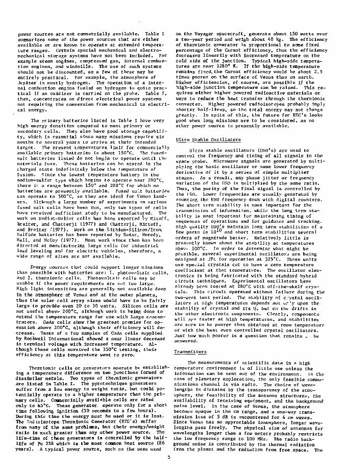
power sources are not commercially available. Table Isummarizes some of the power sources that are eitheravailable or are known to operate at extended tempera-ture ranges. Certain special mechanical and electro-mechanical storage systems have not been included. Forexample steam engines, compressed gas, internal combus-tion engines, and windmills. The use of such systemsshould not be discounted, as a few of these may beentirely practical. For example, the atmosphere ofJupiter is mostly hydrogen. The operation of a inter-nal combustion engine fueled on hydrogen in quite prac-tical if an oxidizer is carried on the probe. Table I,then, concentrates on direct: electrical power systemsnot requiring the conversion from mechanical to electri-cal energy.
The primary batteries listed in Table I have veryhigh energy densities compared to most primary orsecondary cells. They also have good storage capabili-ty, which is essential since many missions require sixmonths to several years to arrive at their intendedtarget. The present temperatures limit for commerciallyavailable primary batteries Is about 150°C. The fused-salt batteries listed do not begin to operate until thematerials fuse. These batteries can be stored in thecharged state indefinitely below the temperature offusion. Since the lowest temperature battery is thesodium-sulfur type which begins to operate near 280°C,there i: a range between 150° and 230°C for which nobatteries are presently available. Fused salt batteriescan operate to 500°C, so they are ideal for Venus land-ers. Although a large number of experiments on variousfused salt cells have been run, only two types of cellshave received sufficient study to be manufactured. Thework on Sodi.im-Sulfur cells has been reported }-y Hitoff,Breiter, and Chatterji (1977) and Chatterji, Mittoff,and Breiter i'1977). Work on the Lithium-SIlicon/Iron,Sulfide batteries has been reported by Sudar, Heredy,Hall, and McCoy (1977). Host work since then has beendirected at manufacturing large cells for industrialload leveling and for electric vehicles, therefore, awide range of sizes are nor available.
Energy sources that could support longer missionsthan possible with batteries are: 1. photovoltaic cells,and 2. thermionic cells. Photovoltaic cells may beusable if the power requirements are not too large.High light intensities are generally not available deepin the atmosphere of Venus and at the outer planets,thus the solar cell array sizes would have to be fairlylarge to provide even 20 to 30 watts. Silicon cells arenot useful above 200°C, although work is being done toextend the temperature range for use with large concen-trators. GaAs cells show the greatest promise for op-eration above 200°C, although their efficiency will de-crease. Tests of a few samples of GaAs cells suppliedby Rockwell International showed a near linear decreasein terminal voltage with increased temperature. Al-though these cells survived the 35O°C testing, theirefficiency at this temperature went to zero.
Thermionic cells or generators operate bv establish-ing a temperature difference on two junctions formed ofdissimilar metals. Two types of thermionic generatorsare listed in Table I. The pyrotechnique generatorssuffer from a low energy to weight ratio, but could po-tentially operate to a higher temperature than the pri-mary cells. Commercially available cells are ratedonly to 65°C. These generator, operate only for a shorttime following ignition (30 seconds to a few hours).During this time the energy must be used or it is lost.The HadLoisotope Thermionic Generator (RTG's) sufferfrom many of the same problems, but their energy/weightratio is much greater than any other power source. Thelife-time of these generators is controlled by the half-life of Pu 238 which is the most common heat source (86years). A typical power source, such as the ones used
on the Voyager spacecraft, generate about 150 watts overa ten-year period and weigh about 40 kg. The efficiencyof thermionic generator is proportional to some fixedpercentage of the Carnot efficiency, thus the efficiencydecreases linearily with increased temperature on thecold side of the junction. Typical high-side tempera-tures are near 1280° K. If the high-side temperatureremains fixed, the Carnot efficiency would be about 2.5times poorer on the surface of Venus than on earth.Higher efficiencies, of course, are possible if thehigh-side junction temperature can be raised. This re-quires either higher powered radioactive materials orways to reduce the heat transfer through the thermionicconverter. Higher powered radioisotopes probably implyshorter half-lives, so the total energy may not changegreatly. In spite of this, the future for RTG's looksgood when long missions are to be considered, as noother power source is presently available.
Ultra Stable Oscillators
Ultra stable oscillators (USO's) are used tocontrol the frequency and timing of all signals in thespace probe. Microwave signals are generated by multi-plying the basic oscillator or some lower frequercyderivative of it by a series of simple multiplierstages. As a result, any phase jitter or frequencyvariation of the IISO is multiplied by the same ratio.Thus, the purity of the final signal is controlled bythe ISO. Lower frequencies are usually generated bycounting the USO frequency down with digital counters.The short term stability is most important for thetransmission of information, while the long term sta-bility is most important for maintaining timing ofsequences of operations and for guidance and tracking.High quality USO's maintain long term stabilities of afew parts in 10*" and short term stabilities severalorders of magnitude better. Relatively little ispresently known about the stability at temperaturesabove 100°C. In order to determine what might bepossible, several experimental oscillators are beingdesigned at JPL for operation at 325°C. These unitsuse special crystals cut to have a zero temperaturecoefficient at that temperature. The oscillator elec-tronics is being fabricated with the standard hybridcircuit techniques. Experimental oscillators havealready been tested at 280°C with off-the-shelf crys-tals. This circuit operated without failure during thetwo-week test period. The stability of crystal oscil-lators at high temperatures depends not or'y upon thestability of crystal and its Q, but on tht drifts inthe other electronic components. Clearly, componentswill ap? faster at high temperatures, and stabilitiesare sure to be poorer than obtained at room temperatureor with the best oven controlled crystal oscillators.Just how much poorer is a question that remains - beanswered.
Transmitters
The measurements of scientific data in a hightemperature environment is of little use unless theinformation can be sent out of the environment. In thecase of planetary exploration, the only feasible commu-nications channel is via radio. The choice of wave-lengths is dictated by the transparency of the atmo-sphere, the feasibility of the antenna structures, theavailability of receiving equipment, and the backgroundnoise level. In the case of Venus, the atmospherebecomes opaque in the cm ranges and a one-way trans-mission loss of 5 dB is encountered for 4 cm waves.Since Venus has no appreciable ionosphere, longer wave-lengths pass freely. The physical size of antennas forwavelengths longer than a few meters probably restrictsthe low frequency range to 100 MHz. The radio back-ground noise is contributed by the thermal radiationfrom the planet and the radiation from free space. The
free space background radiation becomes smaller as the
wavelength is shortened, so shorter wavelengths are
generally preferred. Therefore, any transmitter tech-
nology that can operate in the frequency range from
100 MHz to 3 GHz is a potential candidate for our
purposes. If we restrict our study to devices that
could operate above 150°C, we find only vacuum tube and
GaAs semiconductor devices. In the case of vacuum
tubes, there is no reason to believe that a wide variety
of devices would not work if special precautions were
taken in fabrication. Included as possibilities would
be Klystrons, T W T ' S , and standard ceramic vacuum tubes.
Of these only the ceramic trj'ode vacuum tubes have been
tested to temperatures of 450°C and found usable. A
small pulsed oscillator is being designed and fabricated
by UfiH-r.i] Electric for testing at .TPL. This oscillator
could be used as a beacon, a simple telemetering de-
vice, or possibly a radar altimeter. Vacuum tube de-
vices have the potential or operating at either con-
tinuous low power or high peak pulse power, thus they
are ideal for pulsed radar and beacun applications.
C.aAs transistors are available and provide the
possibility of higher efficiencies than vacuum tubes,
since no heater power is r -quired. •.-aAs transistors
supplied by Microwave Semiconductor Corporation have
been tested at JPL to temperatures as ni^h as 210°C
tor a period ot 10 days with no noticeable deteriora-
tion of the S-band performance. Operation of these
cievices to higher temperatures is likely to be possible
with reduced efficiency.
e transmitter can be designc
uv ..-«i 1....v ..~ .... designer. O
system is not considered to be ut t to point it ar likl
wise, the antenna system is not considered to be u
serious problem, but systems to point it are likely t
be a greater problem.
Electromechanical Devices
Electromechanical devices include such things as
motors, solenoids, relays, resolvers, synchros, and
so forth. Transformers are also usually included as
simple machines even though they do not employ mechan-
ica! motion. Both adequate magnetic materials and
pagnet wire exist for fabrication of transformers for
operation to 500°C. Transformers have been built for
even higher temperatures, however, commercial suppliers
are scarce. Recently, transformers have been built by
General Magnetics Tor testing at JPL for temperatures
to 350°C. These transformers have operated for several
hundred hours at temperatures between 200°C to 300°C.
As a result, we believe that electromagnetic devices
of all types can be designed, i•esently under testing
are several transformers and reed switches. High tem-perature motors were demonstrated by General Electricin the 1950's, but apparently this technology has beenlost. At the present time, few high temperatureelectromechanical devices can be found, but modifica-tions of standard designs 3hould be possible simply bysubstituting high temperature materials for the stan-dard materials.
Deployment Devices
Spacecraft designers have a number of favoritedevices for deploying spacecraft systems. Among theseare various pyrotechnique devices such as explodingbolts. All pyrotechnique materials become increasinglyunstable as the temperature increases, and the use ofsuch devices at high temperatures seems out of thequestion unless insulation or cooling is provided. Anumber of other deployment techniques seem applicable.For example, since the temperature increases as weenter the planetary atmospheres, various fusable pinsand plugs can be used to initiate deployment. Pressuresensitive devices may also be practical.
C o nclusions
There are many appli.cations requiring high temper-ature electronics for space exploration. Presently,there seems to be no applications requiring systemsoperating above 500°C, when very few electronic com-ponents continue to operate. A njmber of importantmis- ions can be carried out with 300°C electronics,most interesting would be the low altitude balloonstudies of the Venus. Even more extraordinary wouldbe a low altitude airplane imaging system flying onlya few hundred meters above the surface. Although itmay be several years before such missions could beconsidered seriously, a balloon system to study theVenusian atmosphere at an altitude of 40 km is beingdesigned by the French Space Agency and initial studiesof JOCC electronics are being carried out at .1P1. fora possible balloon mission near an altitude of 18 km.
Electronic systems that are required includeinstruments, modulators, ultra stable oscillators,transmitters, power supplies, and power sources. Manyof these systems would benefit from further work inhigh temperature semiconductors. Especially lackingare high temperature diode rectifiers and microwavetransistors. New developments in GaAs and CaP deviceswould greatly aid in simplifying the design of hightemperature systems. The ultimate 500°C applicationswill requirr new technology. Further work on SiCsemiconductors seem appropriate. The integratedthermionic circuits being developed by McCormick (197S)at Los Alamos Scientific Laboratory coupled with ceramictriode transmitters by General Electric could providetiie basic building blocks for rhe first entry into thearea of 500°C exploration.
References
1. Chatter jl, D., Mit.'ff, S. P., and Breiter, M. V.,(1977), "Sodium-Sulfur Battery Development atGeneral electric". Report it 77CRD183, GeneralElectric, Aug. 1977.
1. McCormick, J. B., (1978). "High Temperature Elec-tronics Workshop, Progress in the Development ofMicroelectronics for the 500°C Environment",Conference Proc, Jan 4-6, 1978, // LA-74O9-C.
3. Mitoff, S. P., Breiter, M. W., and Chatterji, D.,(1977), "Recent Progress in the Development ofSodium-Sulfur Battery for Utility Applications",Proc. of 12th IECEC, 359-67.
4. Palmer, D. W., (1977), "Hybrid Microcircuitry for300°C Operation", IEEE, FHP-J-2, 252-7.
5. Palmer, D. W., and Heckroan, R. C , (1978),"Extreme Temperature Range Microelectronics", IEEE,CHMT-1, 333-40.
6. Prince, J. L., Draper, B. L., Rapp, E. A., Kronberg,J. N., and Fitch, L. T., (1980), "Performance ofDigital Integrated Circuit Technologies at VeryHigh Temperatures", IEEE, CH 1568-5, 135-44.
7. Sudar, S., Heredy, L. A., Hall, J. C , and McCoy,L. R., "Development Status of Lithium-Silicon/IronSulfide Load Leveling Batteries", Proc. of 12thIECEC, 368-74.
8. Veneruso, A. F. (1979), "High Temperature Tech-nology — Potential, Promise, and Payoff", HighTemperature Electronics and Instrumentation SeminarProceedings, Dfc. 3-4, pps. 17-26.
* This paper presents the results of one phase of research carried out at the Jet Propulsion Laboratory,California Institute of Technology, under Contract No. NAS 7-100, sponsored by tbe National Aeronauticsand Space Administration.
NEEDS FOR HIGH TEMPERATURE ELECTRONICS IN FOSSIL ENERGY PLANTS
W. W. ManaganArgonne National Laboratory
9700 S. Cass AvenneArgonne, Illinois t :39
The purpose of this paper is to present needsfor high temperature electronics in fossil energyplants by first discussing several case historieson applications and second by discussing themeasurement methods. This will present some ofthe typical operating conditions encountered inaddition to temperature as well as the electronicrequirements of high temperature transducers.Emphasis will be placed on unmet measurement needsas identified in a State-of-the-Art Survey.1
Process temperatures in synfuels plants havewide ranges which may be grouped as follows:
1. Ambient (-40°C to + 125°C) (solar plusself heat in enclosures);
2. 800°F (426°C) limit for carbon steelpiping;
3. 15O0-17OO°F (800-925°C) in combustoreffluents;
4. 2500-3200°F, in oxygen fed combustorsand magneto hydrodynamic channels.
Oil and gas well logging tools encounteroperating temperatures of 100°-200°C.Under sodium viewing and signalling infast breeder reactors can be done at400°F (200°C) during loading or shutdownconditions.
Measurement methods include:
1. Ultrasonic, velocity by time differenceand by Doppler effect (using piezoelectrictransducers) as well as noise vibration,erosion and safety related measurements;
2. Electromagnetic induction, pressure gaugesand flowmeters;
3. Capacitive, velocity by cross-correlationand present-by-weight solids in twophase (slurry) flows.
All of these, especially the piezoelectricand capacitive transducers, may benefit substantiallyby placement of preamplifiers or pulser/receiversnear the transducers to transmit high level, lowimpedance analog signals or, in the future, fullydigitized signals.
Future fossil energy plants will requireautomated control for efficiency, safety andenvironmental acceptability. Electronics andtransducers capable of operating at and with-standing temporary high temperatures will be needed.
N. M. O'Fallon, et al., A Study of the Sta'_°-of-the-Art of Instrumentation for Proress Control and Safetyin Large-Scale Coal Gasification, Liquefaction, andFluidized-Bed Combustion Systems, Final Report,ANL-76-4 (January 1976).
HIGH TEMPERATURE ELECTPONICS UTILIZATIONFOR PRESENT AND FUTURE NUCLEAR INSTRUMENTATION
M. Marx HintzeE C £, C Idaho, Inc.P. 0. Box 1625
Idaho Falls, ID 83415
Electronics used in nuclear instrumentation iscompromised by restrictions relative to the environ-ment (temperature, radiation, pressure, etc.).Electronics, by necessity, must be located atconsiderable distances from the measuring point.
There will inevitably be many improvementsmade in instrumenLation and controls because of thethree-mile-island incidenc. Improved electronicscapability will complement this surge for safercontrols.
Other areas, such as diagnostics, will advancerapidly as ability to withstand harsh environmentsbecomes reality. The remoteness of temperaturemeasurement electronics significantly reducestime response. Minimum response time in theinfant controlled fusion plasma diagnostics andcontrol is vital.
Fluid density measurements would benefitfroir electronics mounted close to a gamma densito-meter detector. This would improve response timeand stability.
In conventional nuclear reactor instrumentapplications, a continuing engineering problem isthe large number of pressure boundary penetrationsnecessary. With electronics capable of withstandingsevere environments, the number of penetrationsuould be greatly reduced.
Fiber optics and electronics together capableof resisting temperature and radiation, in thenuclear reactor realm, would greatly enhancemeasurement capability along with reducingmechanical cabling and penetration requirements.
11

HIGH TEMPERATURE ELECTRONIC REQUIREMENTS IN AjjROPROPULS ION SYSTEMS
by Wi [ 1 i am C. Nieberd i ng .ind J . Anthony 1'OWP L1
Nat ion a 1 Aeronaut ics and Spac_* Ad mi n i s t r a t ionLewi s Rese a re h L in t e r
t: 1 eve 1 a nd , Ohio * M 3 5
Summary
Thi s puper d i s c u s s e s the ne^Js 1 or hi gh tempera-t u r e e l e c t r o n i c and e l e e t r o - o p t i c d e v i c e s as theywou Id be used on a i re r a f t t* ng ines m e i t her r e sea r chand development a p p l i c a t i o n s , or o p e r a t l o n a l i p p l i c a -t i o n s . 1 he cone l ' j s ion reached i s r hut the tempera-t ure at which t he d e v i c e s must be a b ie t o lunct ion isin the neighborhood of 50lT Co f-00" t. e i t h . r l o r Ki,Dor tor o p e r a t l o n a 1 a p p l i c a t i o n s . In R&O a p p l i c a t ionstlit' d e v i c e s must t u net ion in t h i s tempt ra t ure ranj'i-when i" the engine but only to r a n o d e r a t ' ' per i od olt i m e . On ,ir. opera t iopa I e n g i n e , t Me re 1 i abi 1 i1 vrequ . rercenr s d i c t a : c rh.it th? d e v i c e s be ab l e to D*»burned- in .at t e m p e i a t u r e s s i g n i l i c a n t l y hi grvr thanLhose a: uh l ch they w i l l tutv:t ion or. t he . n g m c . 11'ema jnr poin t made is t ha t senuconduc .'or teenno 1 ogymust be pushed we 1 1 beyond the U' \v l .it which s i 1 l *. TIw i l l be ab l e t o J u n c t i o n .
Introduc f lon
The purpose ol t h i s paper is t o desc i ibe t heneed s tor hi gh t empernt ure e iec t. ton ic s i n th»- a i i -; r a r1 engine t i e I d . The vi ewpoi nt exprebseci i s asseen trom the Lewi s Mese.-J r<"h <. e n t e r ol NASA I :i l i gh tol the tac t tha t a major element ol t he C e n t e r ' sm i ss i >n is to pei I oixi bas IC r e s e a r c h .md .ieve 1 opranta i -^eii at i.r.provi ng . l e f p r o p u l s L o n systems . 1 hi s vi evis a l s u based on d i s c u s s i o n s ol the t op it with manyot he Aroitps invol ved l n a* ropropu J s J on hot b ingovernment an.) : ndu st ry .
'1 he ma jor a r ea s ot i-e?ea rch aim Jt- ve 1 opine nt inthe a i re ra t t ent, me t ie l i today n n : i P h igher tuci«.• t f I c l en<- v , (2) g r e u er tiurab 11 11 y , and < i) red u ceo.."missions, bot h gaseous and a c o u s t i c . 'I here i s a1 ou r th t;.a jor a rea of *i'rn which i s not t i ed so d i r -c : r i v u 11 h I aburai ory re sea rch .Tt<j deve 1 opracot . JCwith f ly ing o p e r r r i o n a 1 e ngiHe s . 1 'h i s area is I heredu - L I oi. of d i rec t opera t i ng cost vi.i r e d u c t i o n s mthe cos ' of ma I n t ^ n a n c 1 .mil improv-.-meiiL s in «. unt r»»lsys t ems . Thi s may wr 1 L be th«- no^l s i g n i t i c i n t mot I -vat or ol a l l when one get s to t he bottom 1 ine .
In t h i s paper we w i l l end^.j vor t o show that -illthes ' 1 j r e . i s ol worlv, sepa: a t e iy and tog*1 t her , provi uv•strong m o t i v a t i o n lor development ol high temperat : r -e l e c t r o n i c ana olee t ro~op t i c ^ e v i c e s .
Requ ' rements t or Ground Test i ;• __ul £ng ines
In t h i s s e c t i o n we w i l l d i s c u s s the need torhigh . empera tu re • l e c t r o n i c s lor o p e r a t i o n on the hotr o t a t . ^ t u r b i n e d i s k s of e. ng i n c ; used for re sea re hand advanced deve lopr..ent . One u rgent requ i rement i sfor a mult i p l e x e r o p e r a t i n g at 500' to 600° C.
The development of a new a i r c r a t t engine is avery long and expens ive provess• 1 he process cantake as long as 10 y e a r s from s t a r t on ihe draw ingboard t o f i r s t eng ine c e r t i f i e d to f l y . During t h i sp rocess man/ p r o t o t y p e s a re b u i l t for t e s t i n g anddeve 1 opine nt purpose 5. 1 lies t-' p r o t o t y p e s, as we II asi nd i v idual engine components, 2 re opera ted r epea t ed l yin ground t e s t f a c i l i t i e s . For each of these t e s truns rhe engine or component i s i n s t rumented with themaximtKP number of s enso r s p o s s i b l e so that as much of
the des i red in I orm.it 1 o\i as puss ib l t 1 i s ubt ai ned i rowe.ii-n iac 1 1 1 Ly run- hv-ii n i t e r an eng ine ;_ . T t n u - d* or I 1 ight , prob 1 ens a n s f in i t s opera t IO.I on d i r -1. ra l t , or •.•ays ol improvi ng i t s ope ra t iona I charac -t e n st ics beoone apparent so tha t t h i s t e s t ;n^ p r o -ce s s c out i nues we 1 i in!*' the use * u 1 L11 e ol nv. eng memode J . An fxarnpl c i>; t )i 1 s 1 . t he H£F/V^ program u ; n -Juc te<i h'- NASA to mod 1 ty en^ 1 n«-s . _ !;e those i'i, ttieUl 9 a nil tile Bue 1 ng 72 7 t o rvtii,^ e t he acou^t i t no : s f .This model -"lit i n ' ' ha*i been in s e r v i c * tor many year^nut 11 v prt»:,suri'b gene r a t e d oy e r vi ronnent a i concernsm.ule it dt -1 r.ib 1 e L (• £,u back and r»- J e s ign par L s ot ; tI or reduCfij noisi- ems ,s,s ion- 1 hi s pr< ^ r .m, by t heway, leti to the tr.provt-'d enj: : n.- now on ch. net.^[ re tch«»d Dt c .
Ttu net re suI t 01 «i II t h i s i s t nat eng ine Jnoeng 1 :ie .-omponent - rece 1 ve a lot ot t e s t 1 n^ and t h i s1 s .i very ••xpens i ve pro<~-".s.-- An inii i vi du,i I newf-.i! \ nt c ;ir. v . >t n »ew mi l l ion doi 1 ar s per 1: opv - i tc ;J;I t .ike r he or^ier oi twent v ol t iie-se to ^ one up wit hthe f i r s t cer Z 1 1 lab ie c o p / . The cos t to -sr a own ;;n<• nj; . ' ' • , put in new s n; T S and w: r 1 ng . .ind r^bn 1 1 dI ur iapothur LL-.- L run i^ f nuent ly upward oi aiju.ir t er m 1 1 1 1 on iiol l a r ^ • ' t op v>t a l l t h i s i s t he1 JC t t iiat the cos t or per tortni ng the i«- st run 11 si-1:i.s sky rocket ing because ot tl.« r 1 s 1 n;: s" «*• ot e..g i r e:i.i'I aiid Lest lac 1 1 i ty opt r-it 1 ng pukvr . A t y p i c a l• ng 1 r.e * t*&t s tand capab le <.i a L t 11 =id.- 1 i ; glit s i n u i a -t ion I'SHS upwards ol >U megawatts-
ihese t e s t " . o s t s pro vi de a z t * -rr-'-r.dous impetustow.jrJ get t ing as rj«my senso r : on .in eng ine at i r.et me ,1 s pos s 1 b 1 e in or<ier to reduce t he number oi• e bu 1 ids and r ** st runs . I h 1 s is 3L cent uatt-d ny t het <ic t tha t every rebu 1 Id gen. - r a t e s a poss 1 b ie assembl v>M ror w!ncii on r a r e occa^i< n csn r e s u l t in c«iLas~t rophic t a i l u r e caus ing loss ol eng m.- and , or par t olthe lac 1 i1 ty i t s " 1 \ -
U ;..•?£ curreiif Iy l i m i t s Liw nenber o t s e n s o r svh 1 ch ^11 he i n s t a 11 ed and ut 1 1 1 zed tor one t e s t ; i o.ifiswi'i t h i s one must look nl the c u r r e n t r easons tor>-ng 1 ne Ki,D. As was mention. 1 in (.lie lnt : oduct ion,; wo ol the ma 1 n mot 1 ves tor KiD ar*J reiiuce4; 1 ue !cunsumpt ion, ami g r e a t e r d u r a b i l i t y . In t h i s a roa olu, 1: ., <it-1 -11 1 ed rai'a ..urement s on the i-. t rot at 1 nj* t ur -b i'"*e ,ire r e q u i r e d . The ex amp 1 e we w i l l d i s c u s s i st he need ior da t a 1ron t h i s r u r b i n e . Here 1s wher-t he need i or high tempera t u r e e l e c t r o n i c s . i r i s e s -
A lundame nt a 1 I av of t bernoiiynami c s , t he Carno-ttheorem, s.-ys t h a t grea t t - i e f f i c i e n c y r e s u l t s I ronhigner t u r b i n e i n l e t t e m p e r a t u r e . Another fundament -a 1 law I re l a t ed to t n a t of Murphy) says t h a t hot t e rrot at 1ng machinery i s e i t he r l e s s d u r a b l e or weighsn;ore. Par t of the p r o c e s s , t h e n , of produc ing moree f f i c i e n t and d u r a b l e engine* i s one of obt ai ninginformat ion about the t e m p e r a t u r e s and s t r e s s e s w i t h -in the t u r b i n e to a leve1 of d e t a i I never beforea t t empted . The l eve l of d e t a i l needed in a p a r t i c u -la r s e c t i o n of the engine i s , in i a c t t p ropo r t i ona lto the s e v i ' r i t y of c o n d i t i o n s in t h a t s e c t i o n becausethe marg in for e r r o r i*> l e s s in tnose s e c t i o n s wherethe t e m p e r a t u r e s and s t r e s s e s are the g r e a t e s t . Th isleads to the need for t a r more da t a than ever be fo refrom the t u r b i n e d i s k s and b l a d e s . This i s thehot t e s t pa r t of the engine o the r than the conbus to ri t s e l f . In the t u r b i n e the t e m p e r a t u r e s a r e not only
13
very high bur they are a 1 so very noii'un i form due t o Kequ i remtjrct s for Operational Enginescool i ng i low tl'rough sma 13 bleed hu les w:r ht n i a*-b l a d e s - lit t h i s s e c t i o n we w i l l dt-vt- l o p t h e n e e d s i o r
t h e s e v e r y sarnt- c o n d i t i o n ? t h i t make I IJ J 1 fii^ti t emper a t u n 1 e l c e t r o n i c s on o p e r a t l o n a 1 er.g i n e s .i n s t r u m e n t a t i o n o t t h e t u r b i n e m a n d a t o r y a l s o make fcven t tu iugU we w i 1 i a r r i v e a t t r ie s j r . t ' I e n p » T 3 t « r ere 1 i a b l e i n s t r u m e n t a t i o n mos t J i J i i c i ; ! ' . . In a t i . r - U-vvi r c q u i ro r . , - iu o t ^00 t o fcOt'" t , i t u i i j be t o r ab i n e t e s t at " h i s i yp»' , • t i s c e c e s s a r v t o o b t n i n ii i f t e r e n t n - a s o a . Tiii- : unc t i o m ng t e m p e r a : u r e lev** Id a t a t ron> t h e .->nie: <?: >>ne hurid r eu s e n s o r s , 1 l ke . : t Me . ' i . - a r ' : i : c s on .in o p . - r a t m £ e n g i n e w i l l bet b f rooc<HipU '« anu s t r a i n g a g e s , mount eo on t he ro t .jt - jbo i ; r J< ' J • ir. r e i t a b i 11 t y wi i I d i c t a t e a muchi ng b l . t i i . s a r a i n s k * » . A i l t h e se .st n s o r s e.*n be f;; ^h . - : a- . r : ; - ir. t e r . p e r < i t u r e .m o u n t e d but r«>«it i n?; t in- l e a d w o r k b e e o n e s in pus s i:; 1 ••. 'i h> ' • -*t s : b . i i i c a n t p r o b l»-r.; u i t h o p e r . j i l o n a IOne i s r a c e d w i t h r* ' I ng a I eu hui Jre<f u i r e iiowii . ) . . . r . i t t e : v u v - tv-Uay i s t h a t th- -1 r d i r e c t c p e r a e i ng! rotn t h e b l a d e * a tW, . .v *ii>k I *> r he . - . h a U . F r o n h e r e • ' s i - , .«:< t o o h t ^ n an.i g e t t i n g h i g h e r . U * r t a i n l > t r.e: hev mu^t b~ r o u t e d th r "u j ;h a h^ !•• ir, t h - i.o 1 !• ,w n . M nj: s. • '.-ii : ! u.- J i s a m a j o r c u n t r i b u t u r t o t h i ssii . i l t out t o some t n n s m i r-s j on c H - v i ^ 1 s u c h .is .i s l i p pr<.-b I rr,. a x •> t he r o o t r e a s o n I a r t h e R&J) l ^ e n a tr . fii< 3 -..sfrtth I -. o r t»- leme i r v ti».-v: c»- t o g e t r he d.ii s :«'0>J< « .' lu t - i consurcp t i o n . l l oux 'v t r . t\je 1 c o s t s a r ef roin th.- r o t a t i n^. . s n a t t t o t h e s t i l t i>nwry ii-Tf-1 h.*:;- t"'1* tn> . n I v r..i j o r i. >nst i tm-p . t o t , r ^ c t o p e r a t l n ^: i i rv -'(|ii I [.>[:;«• nt . "I h*1 p r o b U»\.i l > l i i a t t fj'- (;c V i s c. m ^ •>-,[. Anot h.-r n<- JOI I ae t o r i s t^ng in»- n a j n t e n s n i e*sri.i i i .ind >>i t h«- w i n " ; a n - : *»,? t ^ »ok . If t h«- no !•• i s A-, ; n.- rn i : i •>• s b^iror:*- p.or»- 6Oph i s t t c a t e d an*i c c n p l exir.;'.' i '•• i ;;>;•* r , t h** .sha 1 Z h.t s t oi> 1 111 i »• s t r.- n » t h .in.l in r fn- m t i - H ' s t *>l rt-tiut '^JI I i;e 1 rnnsu t f .p t i o n anil i o'-t-r, r nit-. h.ifi i L'.T . r e s'.'.iafK t r«'cjii**ns. i>- '"".•;. i n t o 1 i .• i v vi-1 ^iii , ; i i c v .i 3 s«* JK-C J C I - nort? d i t I t c u t t ar.ti, c o s t 1 y t oid ?>;••;"(- s n ^ u u - . s . 11 t ti.- wi r**s .ir<' n.nit- t o o ! i u : \ '•••i i n M i r : . Jf; i s fsas i *-d t o »»mpha »i s or. j ; r f j t e r Otjr -
r h.-. f: r.-,ik . : r iu- r in i us ' , .i 11 a t loi'i am: . 'or i ;i npi>r.i - .»*n ! 11 > .tn*1 t o n . ; t : i ; ; a r i z-i; i on <>r t'nt; 1.10 t i f s igv-&*t i •• . un : t ; ) . i imdi i^ ' t h i s p ' - . ihU' tn , : n * u I i s e a i*' • ;v,', i n* . ^ \ - , n i s . - wi- .->.-(--. 1 ,• be n.ir.n*-r i r\£. away a t C o s t s so11 --,t i :m . i : t hr i d t t * h.i L t l i c r c i s r.o t e i <-mi' t ry *v - - r..inl ho n - , t hi- r e a d e r n ^ ' i i^t t he inp r«?s s i o n t h a t; •-'- i v . I ! .tb 1 .• t -Hi.}. ., in h j > L- ap. th ;*• .<; h.nuj i i n ^ -i; i ; h.'s*- ^n»h 1 i/ns -ipp 1 y pr i n : ^ r i l y t o t « e c i v i t i a r .tfi .-sf r ' l . i n n . ' 1 . , : -r <:.ii ,i s it:;u 1 C an<--iti s 1 v w-. X h<- - . . -v - : t ! 1 t-.-t . Nor si..- 7 ,'J« n i ' i t a r y i s a t o a c u t - 1 lv u ' a -• • v i r . c n c h * v h e n - i t r.u s t ,it I oc a t »'•.!. >• ••' •-*•'! ui r ii I in- M- ^ OSC p : ob I nis b o t ti bee a u s e o l t tio »r
; nt u i r n - n t p r a c t ici- i s i.» i n n v , . i l l t \\>- v i n s *><o. •• t « . M I S : r a i r,t *, a:ni b e c a i i s - th i -v a r e t iy m u tti ,-:,'.•- ti i sV but c on n e t t on 1 v is t:;am .is c .*n St- i it • .-; , r i i 's t s i ' f . M s i iv ra ' fC *ng l le s wh; ct. h a v v ;:vJi y e t
t< r - 'u , :h i t l , roiif , i i t iu- uti.n t . AJ t«.-: l e s t i n^ i s v o n p j t T .• ;• v*- I >)[:••• I !;.- r .at ur i t y .i;-..i r e : i r,. r . - n l (>: J e s i j t i t h a t•- s ; f- t h i s ; L o u t t x u r . j t i on , I he »'!1K i n<* i s c k>t n dn-«r isu , i \ •. l.-.i*: - t o l e a i i n - d r«u n t o n . i n c . v i s ; s -- . - ' . e l v t .' a l i o v vn i i i i f c t i ri^' a n o t h e i ' i n t c l i o t t t\t h u, .; >. •- .-n>' ^r.<"~ vh«'ii Co pu '. 1 an e n ^ i r . e I r u n
- j i • ^ . T h i s p r o c e s •' i s r e p e a t ed n ; i \ bt- t Uri-t t o t i vi ' - i r u i ' i 1 jn*i t - . j r 11 down ; o r " a i n t^n . i r i f o . Tn»- n u s t
[ i ; -es u n t i 1 . i l l t in- d a t <i i s o b t a i n«-ii. Itot o n l y i .s M I . - - . T I , r I t .-I I . MI I S t h a t a p a r t I C J l . i r v c n p o n e n i o !; h i .1 t e f r i b I". **x p e n s , vt1 proct* s s but bv t he t irn-- you t * *• iTip in** h.is op t - i a t **£ lot a p r e d o t e r n ; j n»?d ni jnh^r o t
,•••• ti. t he t h I rt: o r : on - t h r ' - a s s c n b l v o t th** «'nj: tn>- . :.>u: s or i v d c s . A i . u t i i r r e o r . n m L r i t**r i o n vh.» cf; i sn.iiiv ol t lit' s e n s o r s and / o r w; r<-? fi.-jvf ( j i l--d 1 r^ r . -,^t- ; I , d^ t» r - a n e when t o r c n o v t ' ar. <'nK: He : s t it a ti-1 t h e r t he n < o r s nt t <- s t l n^ o r t ho s. o i d i sas is« 'nf 1 .' ' '..' r e q u i r e d t h r u s t «. . i n ^ t be a c h i ovvd w, t ' l ou t
.mo «i s.s>'inb J v . I h i s iviio 1 e s 11 u. i t ; on i s '••?} vtiMt*; i v ; int I'xli.m st ^ b r<.*r;|H-ra[ uf e e x c i t - d i n^ .i p e r m s s • b 1 e'.»•,-•• go .»a . .< ' \v 1. 1 n i s t . - n u . e r a i u r e i s n o n i t or J 1 or j u s t t h i s
rtii.u I a r .eet ieu i s -* 1 i*c t r u n IC s w i n c h c an l u n e t i*>si ; I - J : i o s.-. 11 t h i s t e r . p e r a t u r e ^ ' ' ! s £00 hi pi1 th«* £ « r -1.1 t h e e n v i r o n m e n t ;ii t r ie r e g i o n o ! 1 he t u r b t n i ' ->m.- , - J - 1 .*• d r . i M u . i l l y r e d u c e d . i i . v r o j n * o t h o r( i i s ' t . H.-r<j t he t emp.-r . i t ur '"> .ir*' in t h e ;n> 1 >;hbor ho.:d a i t f f i . i vtseti I<^r rer-.TVin^ <3-*3 ^n^ int.- s u e d a s t i'-eo t S0i> : > bOO' (" and t h e com ri p c t . j I , i c c c I ••r.-it 1 on*; he l e i . ; tin i>t s t r JDJ ; I - i o o k i n c ' 1 an<<> o r st- o 1 ro r . t he,ir»- l e i ) , or t hoti.s.jncj s o i t ' s . What i s n«*<*»le'i n o s t t .* i 1 j>i pe r r t h e ••nt s s i on i»t a t y p i c a 1 iy c a c o p h o n o u s
u r g e n t ly i s a n u 11 i p i i -xcr s o t l ia t a l l t ho s o n s o r H .-..n •.*.»«; TUI - a-.d vi i>T,it i o n s . Though t h e s e wi I I no t beb e r-' .h; ' u t *i u r i ng .. m n^ l e t e s t r ' i n . (... ven n i c <. o«« ui*ir*'»l - - i ^ r . i l i c a n t i o r t he p u r p o s e s o i t h i s
t e c h n o I o^v t o bu i 1'J liit- mul t l p l e x e r , t h*1 n<*xt i t <-r. o i p.ip«*r , t h e y a r e u s u a l 1> c o n s i d e r e d uigt-nt in Zi\<i n t e r t - s t m.iy be -,one torn i>i .i».il<?g Co j i ^ 11 a 1 c o n - e x t recv.e bv ti*ost* a b o a r J t iu- .31 re rat z .v e r t e r c ap. ib l e o i hand J i ng t h<* n i J I i vo i t l e w ! s i ^ - itu- a p p r o a c h e s t o n , i i n t - n - m c i - *U»sc r i bed a b o v en a l s i rom the r^"-o<. o u p l i - s . Acid 11 ion.* 1 ly , a h i j ;h t I T . - m e nu t n e c e s s a r i 1 y c o s t e 11 e c t l ve . 'I he t ac t t h a t an
p e r a t t i ro c e Lori*-1 rv sy s t ern t o StMjd t he s i g n . i i . s I r o n onj; i a. h.»s o p e r a t e d l o r a ^ i w n n u n b e r o : h o u r s o rt h e r o t a t i n g s h a l l t o <i s t a t i o n a r y r e c e i v e r w.xj lil be c ; . i l . " i s a v s n o t hinij; ° i t n e cond 11 i o n s u n d t r whi cti ith i g h l y d e s i r a b l e . 1h>- i d e a l wou 1<1 be o n e t h.it o p e r a t e d - l-i t lie i n t e r e s t o i s a l v t y , t h e ^ e i n t e r v.-j J sr e q u i r e s n o c o a h n>; bee a u s e g e t t j n^; c o o l n i g , n r t i ov j r e u s u . i l 1 , s o t s h o r t e r t h a n r c i 11 y n e c e s s a r y s o t h a tt o t h e s e r e g i o n s i n o t ,?n ly c o m p l e x a n d ex p e n s i v«- ma I nt o n a n c e i s i r e q u e n t ly p e r i o r n e d on a n e n ^ i ne t h a tbut a l so tin? cool ; us '*ir I low 11 se i t upset s t he eon- re.i 1 ; y d^e^ not need i t . Exhaust g.is ienpt-rat ure is
d i t ions in the engine t > some extent . It show 1*1 be on J > ./ very ^ross ind ica to r ot he a 1 th so that I he
aotvd that the cap.ibi 1 i ty tor te lomet ry , nu 11 i - en^; i ne nay be in sore neod ot sa i ntennnce be: ore t h i spiex ing, and ana log to d ig iLai conversion in r his er i t erinn demands i t . An a l t e r n a i i v e approach, win ch
PHV vronment, except for th«- high tfnper.it ore , h;is has been t r te-i with sorn' instance's ot success , i s ana I r^ady b«en demons t ra teu . eng ino r-.on I tor l n^ sy^ten. The ideal woni tor ing sy s -
Whnt we have dese r i bed here is t he need tor ten would be on the *?ng in*?- It should co l l e c t data
riipged e l e c t ron ic s to bo used at sink temper or ures oi on se Jeered engine paraneter s and process t h i s dat^
<ji>o<:t 500° or -IOO^ C. It i s most important t iiat to a turn tha t ind ica tes whether the ong ine needsth. bt- devices work r e l i a b l y for the order ot r>0 to na in tenance , po in t s to ti\c component needing the'.' < - hours at t e s t cond i t i o n s . This is not continuous n.i I ntenr.nce, and , perhaps t spec 11 ies what maintenance
,,j,,tat i on, though, because t yp i ca l t e s t runs I ast I s needed. Such a system, coupled with the raodular-
tfwi 2 to 10 hours . More wi l l be said about r e l i - ity o: modern engines , wi l l allow rapid access to thea.Li I .tv in the next s ec t ion when we deal with the p a r t s needing repa i r or replacement based on ac tua l
problems encountered on engines tha t are on opera- performance d a t a . However, tiie modulari ty reqtiire-t ional a i r c r a f t . men' d i c t a t e s tha t at leas t sooe of the e l e c t r o n i c s
required for engine monitoring be located on theeng ine-
The need for such an engine condition monitoringsystem leads rather directly to the need tor high
tempera t uro e l e c t r o n i c s . The devi ces needed h-^re areI or sensor si gna ! c and 11 i on i ng, s 1 &ri3 1 I r.iasmi ss 1 on ,and a mom Lori rig conK t e r . Compared with t he r e -qu 1 r e m e n t d i s c u s s e d in t h e p r e v i o u s s e c t i oil on g r o u n d
t e s t i ng n e e d s , flit- d e v i c e r e q u 1 remont s d ic t a t e d by
t h i s m o n i t o r i n g s y s t e m a t 1 i r s t a p p e a r t o De q u i t e
ben i g n . Th«?re ar-- l a r f e w e r s e n s o r s n e e d e d . They
a r e p r o b a b l y no' , i n t h e r o t a t i ng en vi r o n m e n i . 1 In
s i gna 1 c o n d i t l a n m ^ , t z.-in^m ss i on , and cum pi it i ng
e q u ipmen t w i l l n o t be 1 uc . i t - -d r i g h t in t he v e r y
hot t e s t p.i r t .s o t t he eng i fie bu t on t he ou t s u i t - c i s i n K
s o m e w h e r e w h e r e r he t e m p e r a t u r e s a r e Inwe r . l a r e 1uI
c op * i d e r .11 i on ->t t h i s sy s t en;, t hough , I «jad s t o t he
c o n e I u s i o n t h a t t he re<|u i rernent s may w 1 i b» .is
d i 1 1 i c u l t to s.it i s t y .
7 hi- opt* r a t i ::g t e m p e r a r *ir- f i j u i : ement s l o r t h i s
n u n I t o r I n g sv s t e n i- MI.I i 1 y J o;nt ou t t o be . i lnn-l HlO i
l o r hi gh p e r t o r n a n u ' m i l i t a r y a i r . r a i * .»: t he pos.s I -
b I e : u t u r e s u p e r son ic t r a n s p o r t . - I r.i s t -MTipei a ; u r e
l s s e t by th-- : . u t t h a t t fie L o l d e s t r i r a v a l I J !> I e a t
m.ix i:nusr. speevi ,md a i t i t ude i s ,.t what i s c .> I 1 n i ram
a i r t e n p i - r a t u r e o r £ o t .i i t i-npt-r.1t u r e .it t he se I '. l gh t
i o:u! 11 l m i s . t Ve rv or her -* v.i J ] at; 1 e 1 1 u jd t e n p e r a t u r c ,
e x c e p t th .U OI t h e 1 .e 1 . i „ h i g h e r . Fue i c o o l in*; o l
tin- e l e L ron 11 s i s now he i ng u.-n-d i.; s^rne C.*M S b*.I
i t ir, i, v u n d e s i r a b l e i r o n t h e s t a n d p o i n t oi c u r r
p l c x i t v , - e i g h t , and It ak p o t e n t ia 1 . Tl :us 3lH" t o
-.DO i seems J r i ' . i ^ o n a i u c i a r ^ t - 1 t .ir t 1 i (;t.t «• :V i ne
m . . n i t . i r i ' l g . 1 . - v i c e s . 1 h i •; l e v e l d o e s n o t se.-tr, v.-rv
s e v e r e u n t i l o n e e on-; IO er .- r h. p r o b l e m oi r e l i a b i l i t y .
rt lie re . l s , i.i [ li-.- p r i 'Vi -'i.h s e c t lop, we • ,vne up w i t h
ope r a t i r;y t line r»'i,'i i r e n e n r s o* a b o u t IV* * h u i r r s , in
t he 111 > lit r.on 11 o r i ng sy s t em we n e e d t h t u i s a n d ^ o 1
h o u r s oi ;i!^so I u t e 1 > t i oub i e t r e e o p e r a t i o n . 1 he
p r i m a r y r e a s o n l o r t i n s i s : h . u you w i l l n o t r e d u c e
n.i i nt i-n.i nee c o s t l 1 y o u r mon Hot i ng ,sv st em I a i 1 s .
f a i l u r e o[ r he n o n i t o r i n j 4 > y s t e n w i l l r - ' s u J t ; n
e 11 h e r prerna t u r o e n g I ,n- r * * p a u o* in m m 11 o r •- nii s v s -
t - n r e p a i r o r , t a r w o r s e t h a n t n e . s e , t h e • n d i c a t m n
t h a t t he i»np i ne i s he a 1 t hv wfu-n i t i s riot . i h i s
1 e n : s t o t he I ne sc ana h i c c o n e I u s i on t h a t ver*-1 h i gh
re 1 i a b i 1 j t v i s i . e e d e d .
(.oimr.on p r a c t i c e i o r a c h u ' V i ng h i g n s v s t c . i r e 1 i -
a b i l i t y t o r a g j ven tunct lonai l> r ipe rot u r e i . t o u s e
c o p p o n e n t s t h a t h a v e b e e n b u r n e d - 1 p. a t a M g p i l i c i n t -
1 v h i g h e r t e m p e r a t u r e i n o r d e r t o weed o u t pur e nt I *i 1
fa i I n n s . The h i g h e r t he bi r n ~ i n t e r n p e r a t u r e , i he
s h o r t e r t h e b u r n ~ i n mus t he t u weed out t he bad
pa rt s. An -acceprab] e bu rn - in t emperat ure wou Id beabout t he same as the x. eraperat ure n-qu l red tor groundt e s t a p p I i c a t ions d i scussed e a r l i e r .
A fu r t he r requ irt-nnint on op* r a t iona I eng inesa r i s e s f rom the need tor more s o ( h i s t ica ted e nglnec o n t : o l sys ems. This is being pursued by go mg t oa l l e lee t ron l c c o n t r o l s . 1 he sr c o n t r o l s a re re-qu I redi n o rde r t-> achi eve peak pe r i onna nee with h i gh e £ t i -c i enc y , i ong 1 i i e , and s.i t e l v . Requ i reme nt s f or -.m od u l a r i t y , t I i g h t s a i e t v , and c on ba t $ u r v i va i> l I 11 vd i c t a t e tha t t h i s c o n t r o l systerv be U>cated on thee n g i n e ' T-i i s put s i t a l s o in an envi ronrmint l i k etha t d i scussed for the n o n i t o r mg system. Indeed t hecont ro1 computer may a l s o be t he moni t o r I n g com-pu te r • Thus, <*ng i tic cont roi requ i rcment.. resu 11 inabout t!'p same envi ronment a 1 and r e l i a b i l i t y needsfor e l e e t ronic d e v i c e s as do those of the moni t o r ingsyst em.
We should poin t out here t ha t t h e r e i s a I so aneed tor opt i r and e l e e t r o ~ o p t ic dev ices to o p e r a t eon the e n g i n e . Thi s need a r i se? pr itnar i 1 y in mi 11 -t a r y a i r c r a f t . F i b e r - o p t I C , r a ther than eleetronicc a b l e , t r a n s m i s s i o n of d a t a from place to place onthe a i re ra t t b r i n g s the s i g n i I i c a n t advant ages ofonhanc ed f reed on from e l e c t rotnagne t IC i n t e r * etenc oand the a b i l i t y t o send da t a over mult i p i e pa thswithout incurring the weight penalt ies of multipleelectronic cables . Since much of the data originateson the ongi ne r at least some of the electro-opt ic
devi ces nnd i iber opt ic bunti les wi i I reside on Cheeng ine and there lore have to operate re 1i ably in thesane thernia 1 envi ronment as the mon it o n ng and con~t r o l v 1 ec I ro*i i c s .
1 o surr.tr.ar i s e t h i s -ec t i o n , t h e n e e d s of o p e r a -
c i o n . i l a i r c r a f t e n g i n e n^ni t o n ng and e o n t r o l d i c t a t e
e ioc t r o n i c and e l e c t r o ~ o p t i c d e v i c e s c a p a b l e o t v e r y
hifth re I , . ib I i i ty wh l l e o p e r a t i n g a t t e m p e r a t u r e s no t
t o o much h i g h e r t hai 300C C. T h i s r e 1 1 a b i111 y re -
qui rented* , we ne 1 i e v e , w i l l r eq i i i r e b u r n - in a t t h e
S((" t o ''IK1' (.' t t-tnpei a t u r o l e v e 1 -
L one 1 u d i n g Kemarks
In t h i s p a p e r we h.ive d l sc usse t i t in* n e e d s t oi
h i g h t . m p e i a t u r e I ' l e c t r o n c s mtii e l e c t r o - o p t ; c s a s
t IIL-V wou Id be u^ed on . i i r c r a f t uiig Iiit^s i n r u s e a r c h ,
deve l o p c e u t , and oper- . t i on . Th. cone 1 u s i on r e a d i e d
i s t h a t t he t e n p e r . i t i. r e .it wh I ci. t h e d e v i c e s must be
a b l e t o * uric t ii>n is- .»bi>ij* i in same e l t h e r t o r R&D or
I oi oper a t i otia 1 a p p l u at i o n s t hough t h e r e a s o n s t o r
a r r i v . ::j; a t tf>' s ,-^t L ma ted t o n p e r a t u r e a r e qui to
J 11 I e r e iU . I ;i K^D app 1 i c a t i e n s t h e d e v i ce.- m i s t
I tine t i on at t h i s t e n p e i . t u r e when in t h e eng i n e out
onl v 1. : <i mode r a t e p e r i ot1 o* t irrse. On an o p e r a t ion -
a 1 eng i ni"", t he r e l i a b i l i t y r e q u i r ement s d i c t a t e t h a t
t he d e v t c.-j; !>c- a o i e tt> be b u r n e d - i n 'it t e i r . p e r a t u r e s
s i pn i t i c a n t 1 y hi g h e r th , in t h o s e a t which t h e y w i l l
' urn t i on on t h-1 eng i ne .
We have been p u r p o s e 1 y vague in <ie t i n i n g t h e
teir.pi-r a : ut e go.i 1 a s be ] r.g a r o u n d SuOL' t o 600" C
nee a u se t h e r e a r e jrg-ur.ient s i or a ^ > a l a h u n d r e d
( l e g r e e s above and be Iow t h i s t e m p e r a t u r e r a n g e . The
ma j oi po i nf to be made i *> tiiat uv must p u s h ve I 1
beyond "he I eve I at wh ich s i 1 i con w i l l be a b l e t o
! u n c t i o n -
As a I i n a l t n o u g h t , we would l i k e t o sa-y t h a t
a l l ot t h i s c o n s t i t u t e s t h e j u s t 1 1 i c a t ion n e e d e d t o
g e t support Jor ,i pi -eg r a n .i irned a t h i g h t e m p e r a t u r e
e l e c t r o n i c s - li p r o b a b l y h a s l i t t l e to do w i t h t h e
most s ign i t ic.*nt ru t u r e - p p l i c a t i ons o l t h e s e d o -
v i c e s * They j r e p r e s e n t 1 v unknown. Cop.s i d e r t h e
or ig I na 1 j u s t i t ic , i t i o n s t o r d e v e l o p i n g i nt<?jz r a t e d
c i r c u i t s . They were t o e n a b l e SITU 1 1 , low power c i r -
cu t t r y l o r . s p a c e c r a t t a p p l t e a t i o n s - As i t h a s t u r n e d
out , t h e y were l n d e e d u s e l u l t o r t h e s e p u r p o s e s b u t
t h e se UM.'S have p r o v e d t o be of t r i v i a l impac t on
soc l e t y r e I ,it I ve to t h e o t h e r , more mundane u s e s to
which t h e y ,-ire now b e i n g a p p l l e d . At Lewis we had a
h i g h t p m p e r a t u r e e l e c t r o n i c s p r o g r a m g o i n g i n t h e
l a t e 00' -*• and ear 1 v 70' s a irncci at the needs ofnue1 ear power systems lor spacecraf t . When t h a t wasno longer support e - the el • •c t ron ies program went downthe tubes with i t . Now we a re s t a r t ing up e s s e n -t i a l l y the same program lor comple te l y di t f e r e n tr e a s o n s . >Je cannot he ip but. l ee 1 t h a t high tempera-tu r e e l e c t r o n i c s wi l l l ndeed have wi de appl i c i t ionnot only to the a r e a s d i sc ussed at t h i s confe rencebut a l s o to t a r rnorf important a r e a s which we lus t donot have t h« v i s ion t o pred ict.
Ke fe renees
1. Avionics, Controls & Human Factors Technology Plan,Vol umt' II - Program Element s Descript ions -NASA, Ot fice oi Aeronautics and Space Tech-nology, 1979.
2. High Temperature Electronics Technofogv, Phase I.R8OAEG212, General Electric Aircraft EngineGroup, 1980.
15
FRESENT AND FUTURE NEEDS IN HIGH TEMPERATURE ELECTRONICSFr-R THE WELL LOCKING INDUSTRY
N. Harold Sanders^•search and Er.cjineerina
Presser Atlas Division
Di t-sser Industrit-s
J J201 West?, -imer
Hou^t.n, TX 77001
":_ll'--V--r- T t i s t h i s requirement t ha t forces the well l*-.g-qmu tool desiqnt.T to design for r e l i a b l e ope ra t ion a t
•< - \\* \ :~;\ \ i i r i i t i ons which have r ir;>i temperature aud to put as much c i r c u i t r y as pos--;-*Hi] !"u*-ir al..ni; with ^nannes --.ible into the small space a v a i l a b l e . To meet t h i s
;;;, vhi vi. twv ; r"vi :i*'d the in- M-pd the- doslqner must have a wide range of semicon~i•-• -it bnn^ f i • ir. d«-T tVi:. -:r<: ater r^cU'i. ' . , j ass ive e l e c t r o n i c components, and d i e l e c t r i c
ma'.-t i . ils -.-ommer c ia l ly a v a i l a b l e . The key point hereis "c >minerc ia 1 a v a i l a b i l i t y " such tha t t oo l s can be.ic*i; lunc-d and then manufactured in s u f f i c i e n t q u a n t i t i e stn :,u{tp<jrt the expanding f ie ld requirements .
A i .arcessiul hiqh temperature lodging tool i s a.-cjmbir.atioji ^! -arious meclianical and e l e c t r o n i c coin-; nni-nts wi^h spi- . ia l cons idera t ion required in thea c n l K a t ' o r r>f meta]s , e las tomers , cable s r p ressurem a l ^ , -eed th rus , as well as e l e c t r o n i c components.Tfie fnllovjnq litnitod d iscuss ion addresses only Asi'^nent of th i s - the electro.. '- c components.
-. :) I
: '. i •
r, •( i
' - . : ! ' • >:
. , ;1i i .
: ;*,. t
* • : I
-.' i , . - '
t ! , . . i .
..nil 1.-
: • . ,
: '. . .
. ! ".
< f
T l i
err
: > •
"I"
tV.
i
w
( t
rn!..> • )
a i i
i ::
1
: t .
1
V
1d
!.
r
i 'i . ' .
i i
! •
. i t
I .- c
• • V 1
r--.|.i ' ' •
1- !
1 •-.•; :
11 <
L '.
t> .
i n ;
", !:
, f
i ! .
1
e'i
l
W
r t
sc t
, . r ,.
i 1 i
i - l I
f ;
i i .
i VI
1 : i .
i r i
] •
i i o
C - X '
a :
k-r
, . ? . :
j l : ,
I i
1 s
i . - r
f
v.
n
< _ •
'.r
•!!•.'] i ()!.ni-T,t * 1 ': ' The Component 3
M . _ , , ,, , . . . . , ' v . • f. 1 -. j "*'hc w «.•; c: rr\! comj ancnt for a downhole locqma
"" ,' *' ' l ' . ' ' tocl is actu. . l lv a functional block, e i t h e r monoli thic. i t ' i : . ; • - • w i: : 1 t••!••..'• w i t ; . I J I a t -• J i l k i - O T I - o u . ' ] • - • • s^~. >r hvbr I i, win ch intecirate" a comolete schematic olock
• t v.\ 1 1 ' it. ut i is i Ti»; - i 'itr. l O i u - n t t c n i i ' L * : i t i . i i • • : . i i r l o v' . . , , intr c fiinalr package characterized and tested for hia«'• ' . ' i : n i i r t i ' ( M o r i l r t p e w t - r . i v j i K i j . i 1 . f ! : i . ' i n : o i r . j b l e . ., , , . ti-ini erature operati'in. This allows maximum utilization
• . • • - r . . . l t : . . i K I m i l t f d t ! ; < i s o n ! f i i ' i n v h ; . ' ! i • u i , i t : i „ . . , ,
( - : available spotce in the pressure sealed housing andi;i VCH addo.J assurance that the system will function
, , , i pr-)perlv aft -r assem>,lv. The other major contributionThf (h.iilt-nuf : . " . . . .
,-_- ,jt t h o functional Liock integration is the improved
,, , reliability obtained with component prescreeninc and; • . ; :<•• I 1 -; wit!: t-. -m: -. '.itjir- . n.<i ; r-.1: '-.iirvr <ihovc •, ,. ' * . i. f . ; ', ; > , ; , . ; . , . ,,-• u> i i"f<i'.j.-t-d number of |>ackace.s wi t/i the resulting fewer
. . . i r\tA' rv'tiiino<jts .;: : .)•.••• . i i . . : v> • i •: i i r.i t <•,; i : . :, : n i l ^ c j ; t l i ' i H , t i l ' -• : • ; • i . ; 1 t - i ::••; i M - d a i , i - i | t j j t . - ! b ' . 1 ' . T i v j u . e e r -
' ' " Some types of electronic functions which are uti-. ' - \ i z«-d rir.fi net-cicd for do"rfnholo too l s include the follow—
t . ; i i v > i , , t n . i : : , • • t ' I ' I . H P I . 1
-i v i c t ^ ^ m t !ini - l^- ' r f o i ! , / 1 1
:. t h . i t .-ar-, b<.- a.- SJ: tt ••(.-1 v I un
I 1 ! , • : i V i - l «. 1 i a b : < ' { •"• - '•• I ' n i c i ' u ' ' •
. • 1 , . . r I 1 • • i t " • h , l ' . • 1 : ' , 1 f l t ,5 r t I • :
1 . Vol tat:*.* Regu la to r s - l i n e a r and swi t ch inq
Prec : s ion Veil ta<:e P^ for once
• • - — •• - - ^ I n s t r u m e n t a t i o n ;»mi l i f i c r rfith lOOdB CMRR
My l.an t h - loe: v e i l r u t rm re severe tern- 4 ' r t o A a n d A t o D ' 1 2 B l t Conve r t e r s• :MI : --int-i-.t. sii the too l . ; , bur tfi< need t'1
• 11 i -IU dt wr town r is Hi--+-at'd 'J' W l t ' c Panr:width Ope ra t i ona l Ampl i f i e r w i th tempera-. . . , , . t a r e r t a b l e bandwidth and o f f s e t
a ri uinbei '..-• >' I I : •*rf i i t t o o 1 s be t u n i n combi na* i uii.-. i -HI I f I< *.j>; l u-> i UIJ . Th j .s n e e d h a s in c r e a t e d t h e
, , , , C. P r e c i s i o n C o m p a r a t orU - x i t y of t h e ft* I s by r e q u i r i n g e x t e n s i v e a r . a l f« ; '
sy.st-eir to transmit the larce amounts ? " H i t j h Current . Wide Band Linear Driver•: i <ffi.i i • •o ru i 11.1 o r . i r u : , a s w e 1 1 d s tfi»- a d d i t i o n u f a d i >i i -
t c i i t"< i rmnun i : ; a t , I i •!,-• s'/:-. t-eir t ( j t r t i n s m i t t i i e 1 a r q e a m o u n
r,t . - . o n n o r d a t a t o t h e . u i f a c t - o v e r t h e 1 l m i t e d n u m b e r
:,i iim-s availuM.- > r, t ho Jewing .-able. B- P h a s e Sensitive Detector
lm.reas.-ri com, J,,Xity l n the tool ^iectron, cs would 9 " FET Switch and Driver with low leakage and ONncrnally mean an in.--ri.-asc. in thi- t. „] U-nqth since resis tanceir illcti h -, Iu 1 lmi f .it ions r e s t r i c t tile maximum too] d i -
« t , r . How.-v.r, to ,,-rfuce tool Ktrir.q length and 1 0 - S a m - J l e a t l d H o l d
weiqht, liinphti-iis I-• : l^ced on elimination of flanks andthe min ia tmiza t i >n • f e lectronics throuqh the use of Logic familymedium and larqe •.••r<i 1*. integrated ci i emits and the com-bmat ion of If , and .iu.cretr- cnmioncntS into hybrid 1 2 " C r y S t a l c ™ " ° ^ Osci l la tor
mi c roc i rcu i t s -13. V to F Converter
17
Preferred specifications at 200°C for the functionslisted would be the sane as for better parts presentlyavailable at 125°C. Operation with some specificationdegradation to 250°C would be acceptable.
Relay- in downhole tools are kept to a minimum,but if made more reliable, would be used. A holdingrelay which dissipates power only when actuated isdesirable. At least a DPDT, crystal can size relay withself-wiping contacts for dry circuit to one amp loadsis needed. More poles and smaller size (TO-5) would bea bonus.
SCRs capable of switching up to 35 amps of currentand blocking 800 volts with less than 2.5 milliampsleakage at 25C°C are needed for power control and con-trol of capacitor discharge.
Diodes
With many of the radiation logging tools requiringhigh voltages, t',iere is a particular need for rectif i erswith reverse breakdown voltages greater than 3000 voltsat leakage currents less than 25 microamps at 2SO°C.It is expected that GaP devices might fill this require-ment, but they have remained as laboratory specimensrather than commercial catalog items.
Capacibors
Capacitors with the low dissipation factor of Tef-lon (0.5%) over temperature, the TC of NPO Ceramic(+_ 30 ppm/°C) and a high volumetric efficiency areneeded. Capacitors with these characteristics areneeded particularly for applications such as activefilters and sample and hold circuits. Although RubyMica offers the low dissipation factor and high tempera-ture operation, its TC exceeds the desired f30 ppm.
Resistors
Fixed resistors using metal films have operatedsatisfactorily up to 250°C and beyond, but a trimmerpotentiometer is needed that will maintain its settingover this same range of temperature. Since thick filmresistive elements on ceramic are suitable for hightemperature, the major factor in obtaining such a deviceis in the mechanical design of the contact and drivemechanism to maintain the precise setting over such awide temperature range.
Although selection of fixed resistors to compensatefor circuit variations is an obvious alternative, itgives considerable difficulty in field calibration andalignment.
Magnetics
or to isolate an electrode from an adjacent conductivehousing. For temperatures up to 200°C this has beenaccomplished by use of epoxy/polyimide glass laminatebecause of its mechanical strength and its ability tobe machined to precise dimension in any shape. Theepoxies presently used begin to deteriorate rapidlywith storage at temperatures above 200°C so new mate-rials are needed to extend ttiis capability.
Conclusion
New developments and increased vendor interest lnhigh temperature electronics have definitely improvedthe ctvailability of components for hostile environmentequipment. Tiis paper has .ittempted to show that themarket continues t~ expand and opportunities exist forthe continued growth of commercial r.-roducts in welllogging services.
References
1. Paul Sinclair, "Service Company Needs" Sandia Lab-oratories High Temperature Electronics and Instru-mentation Seminar Proceedings, SAND 80-0834C,December, 1979.
Inductor and transformer design with existing ma-terials has allowed for operation up to 200°C for sometime. Operation above this temperature for extendedperiods awaits the development of more stable magneticmaterials and higher temperature wire insulation.Although the designer can remove transformers from mostsmall signal circuitry, the need for power transformersfor low loss conversion of downhole supply power isstill important.
Dielectric Materials
In several types of logging tools, there is a needto fabricate portions of the tool from a dielectricmaterial to permit the transmission of electric fields
18
S E S S I O N I I
D E V I C ES
Chairman:
Or . 5. VJ. DeppIBM Research LaboratorySan Jose, California
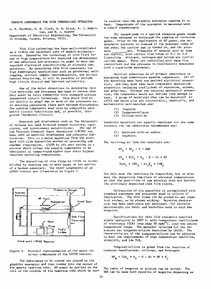
PASSIVE COMPONENTS FOR HIGH TEMPERATURE OPERATION
L. S. Raymond, D. R. Clark, D. 0. Black, D. J. Hamil-ton, and W. J. Kerwin
Department of Electrical Engineering, The Universityof Arizona, Tucson, Arizona, 35721.
Thin film technology has been well-establishedas a viable and necessary part of modern microelec-tronics. Extending the technology of thin films foruse at high temperatures has required the developmentof new materials and processes in order to meet therequired electrical specifications at elevated tem-peratures. By developing thin film components forhigh temperature applications such as geothermal well-logging, aircraft engine instrumentation, and nuclearreactor monitoring, it will be possible to providehigh circuit density and improved reliability.
One of the major objectives in developing thinfilm materials and processes has been to ensure thatthey would be fully compatible with standard siliconintegrated circuit technology. This would lead tothe ability to adapt one or more of the processes in-to existing processing lines with minimum disturbance.The passive components must also be compatible withhybrid circuit fabrication and, if possible, Inte-grated Thermionic Circuits.
Research and development work at The Universityof Arizona has been directed toward resistors, capa-citors, and interconnect metalizations. The use ofLow Pressure Chemical Vapor Deposition (LPCVD) hasbeen used in material development and component fab-rication. This is a major departure from the stan-dard thin film deposition method of sputtering andthermal evaporation. LPCVD by its very nature is aprocess which allows the passive components to befabricated at temperatures higher than their highestrequired operating temperature.
The deposition of thin films by LPCVD is accom-plished by reacting one or more gases on the surfaceof a heated substrate. The raajor components of anLPDVD reactor are illustrated in Figure 1.
Load Ooor
Cold wall LPCVO R.aotor
Figure 1. Pictoral representation of the major in-ternal components of the LPCVD reactor.
The substrates to be coated are placed on thegraphite susceptor and then loaded into the center ofthe quartz reaction tube. RF power is applied to thecoil on the outside of the reaction tube which in turn
is coupled into the graphite susceptor causing it toheat. Temperature of the susceptor is measured witha type-K thermocouple.
The: vacuum pump is a special chemical-grade rough-ing pump designed to withstand the pumping of corrosivegases. Prior to the application of RF power, the at-mospheric pressure is reduced to the pressure limit ofthe pump; the carrier gas is turned on, and the- pres-sure set. Pressures of several torr or lessare typical, with carrier flow rates of 0.1 to 2.0liters/min. Nitrogen, hydrogen and helium are typiralcarrier gases. These are controlled with mass floucontrollers and the pressure is continuously monitoredwith a capacitive manometer.
Material selection is of primary importance indesigning high temperature passive components. All ofthe materials must have the desired electrical proper-ties, and they must also have compatible mechanicalproperties including coefficient of expansion, stress,and adherence. Without the required mechanical proper-ties, the components would not survive long enough totest. A group of materials that can be deposited byLPCVD and which also are electrically, chemically, andmechanically well-matched are:
(1) Tungsten(2) Tungsten-silicon(3) Silicon nitride
Substrate materials are equally important for the samereasons; the two substrates recommended are:
O ) Oxidized silicon wafers(2) Sapphire.
The reactions to form the materials are:
WF, + 3H- -• K + 6HFb £
WF + SiH4 + H, • W - Si + HF
Not only must the materials be compatible, but so alsomust the deposition reactions at elevated temperaturesso that the deposition of one material does not destroythe previously deposited thin film layers.
Delineation of the materials is accomplished withstandard equipment and processes used in silicon ICfabrication. The thin films can be etched by wet chem-ical etches, or by plasma etching. Negative photore-sist has been used since the developer.- for positivephotoresists are basic and therefore tend to etch thetungsten.
Specifications for thin film resistors requiredstable operation to 500° C. with temperature coefficientsof resistance (TCR) less than 50 ppm/°C. over the entiretemperature range. The material selected for the re-sistors was tungsten-silicon deposited by LPCVD. Thecharacteristics of the tungsten-silicon can be adjustedto meet the requirements of high temperature operation,stability, and low TCR.
Tungsten-silicon is grown from the reaction oftungsten hexafluoride, silicone, and hydrogen:
WFft + SiH4 + -* W - Si + HF +
The ratio of tungsten to silicon can be varied. TheTCR can be made both positive or negative depending on
21
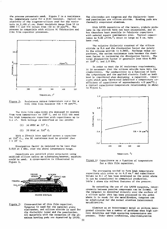
the process parameters used. Figure 2 is a resistancevs. temperature curve for a W-Si resistor. Typical re-sistivity of the tungsten-silicon used for the resis-tors is 2,500 pfi.cm. Sheet resistors range from 50 to1000 n/H and TCR values from -50 to 50 ppm/°C. Theprocess is compatible with silicon IC fabrication andthin film capacitor processes.
The electrodes are tungsten and the dielectric layerand passivation are silicon nitride. Bonding pads arethermally evaporated aluminum.
With LPCVD deposition of the layers, pinhole prob-lems in the nitride have not been encountered, and ithas therefore been possible to fabricate capacitorswith several square centimeters area. Typical capaci-tance is 0.02 uF/cm.2; a r e a B a s large as 4 cm. havebeen u'ied.
The relative dielectric constant of the siliconnitride is 8.6 and the dissipation factor due solelyto the silicon nitride is 0.0002. Forlarge value ca-pacitors, the series resistance term becomes the domi-nant factor in increasing the dissipation factor. Thetotal dissipation factor is generally less than 0.003at 350° C. and 2.0 KHz.
In order to meet the DC resistance requirements,it is necessary that the silicon nitride have very lowconductivity. The conductivity is a function of boththe temperature and the applied electric field so bothmust be considered when designing a capacitor. Capac-itors which were fabricated exhibited a temperature co-efficient of capacitance of approximately +70 ppm/°C;a typical capacitance-temperature relationship is shownin Figure 4.
Tenperatjre, c
Resistance versus temperature cur/e for aW-Si thin film resistor TCR = +6 ppro/°C.
The thin film capacitors are designed to operatefrom room temperature to 350° C. and to fill the needfor high temperaLure capacitor with capacitance up to0.1 uF. Work voltage is specified at twu points:
(1) 50 WVDC ar 25° C,
(2) 20 WVDC at 350° C.
With a 20-volt bias applied across a capacitorat 350° C , the DC resistance must be greater than1 x 10^ TJ.
Dissipation factor is required to be less than0.010 at 1 KHz. over the above temperature range.
Capacitors arr parallel plate structures usingoxidized silicon wafers as substrates; however, sapphirecould be used. A cross-section is illustrated inFigure 3.
TeaperRcure, C
Fipure 4: Capacitance as a function of temperaturefor a thin film capacitor.
ALUMINUMCONTACT PADS
SILICON SUBSTRATE
Cross-section of thin film capacitor.Tungsten is used for the parallel plateelectrodes, and silicon nitride is used forthe dielectric layer and the passivation.All materials with the exception of the al-uminum bonding pads are deposited by LPCVD,
The processing needed to form high temperaturecapacitors with areas up to 4.0 cm.2 and capacitancevalues to 0.1 uF has been developed to the point whereit can be transferred to commercial production.Table I shows the salient features of the process.
By extending the use of the LPCVD tungsten, inter-connects between passive components can be formed. Ifthe tungsten is deposited directly over the surface ofa silicon wafer that has been processed to the pointwhere it is ready for the metallization, tungsten canbe substituted for the normal aluminum interconnectmetallization.
Aluminum as an interconnect metal on silicon inte-grated circuits has a number of problems when high cur-rent densities and high operating temperatures arepresent. Under these conditions, electromi>;ration
22
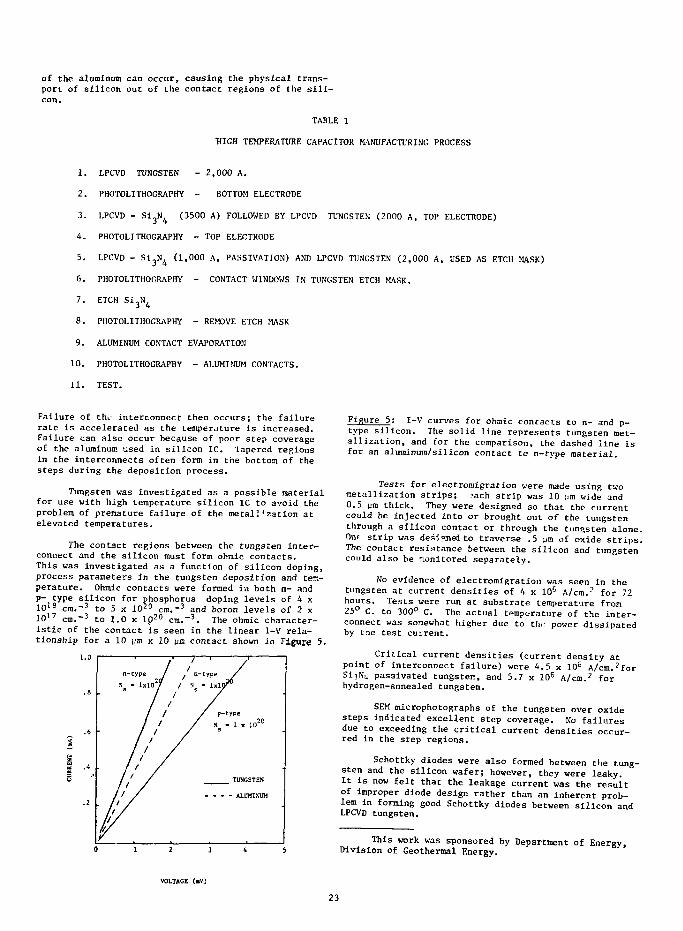
of the aluminum can occur, causing the physical trans-port of silicon out of the contact regions of the sili-con.
TABLE I
"HIGH TEMPERATURE CAPACITOR MANUFACTURING PROCESS
1. LPCVD TUNGSTEN - 2,000 A.
2. PHOTOLITHOGRAPHY - BOTTOM ELECTRODE
3. LPCVD - Si3N4 (3500 A) FOLLOWED BY LPCVD TUNGSTEN (2000 A, TOP ELECTRODE)
4. PHOTOLITHOGRAPHY - TOP ELECTRODE
5. LPCVD - SijN^ (1,000 A, PASSIVATION) AND LPCVD TUNGSTEN (2,000 A, USED AS ETCH MASK)
6. PHOTOLITHOGRAPHY - CONTACT WINDOWS IN TUNGSTEN ETCH MASK.
7. ETCH Si3N4
8. PHOTOLITHOGRAPHY - REMOVE ETCH MASK
9. ALUMINUM CONTACT EVAPORATION
10. PHOTOLITHOGRAPHY - ALUMINUM CONTACTS.
11. TEST.
Failure of thi.- interconnect then occurs; the failurerate is accelerated as the temperature is increased.Failure can also occur because of poor step coverageof the aluminum used in silicon IC. lapered regionsin the interconnects often form in the bottom of thesteps during the deposition process.
Tungsten was investigated as a possible materialfor use with high temperature silicon IC to avoid theproblem of premature failure of the metall'zation atelevated temperatures.
The contact regions between the tungsten inter-connect and the silicon must form ohraic contacts.This was investigated as a function of silicon doping,process parameters in the tungsten deposition and tem-perature. Ohmic contacts were formed in both n- andp- type silicon for phosphorus doping levels of 4 x10'8 -3 to 5 x 10¹⁰ 1 7 cm."3 to 1.0 x 1020 cm."3
phosphorus doping levels o1 cm. and boron levels oof 2 x
The ohmic character-istic of the contact is seen in the linear I-V rela-tionship for a 10 vm Y. 10 um contact shown in Figure 5>
ALUMINUM
Figure 5: I-V curves for ohmic contacts to n- and p-type silicon. The solid line represents tungsten met-allization, and for the comparison, the dashed line isfor an aluminum/silicon contact to n-type material.
Tests for electromigration were made using twometallization strips; ?ach strip was 10 um wide and0.5 pm thick. They were designed so that the currentcould be injected into or brought out of the tungstenthrough a silicon contact or through the tungsten alone.One strip was designed to traverse .5 vim of oxide strips.The contact resistance between the silicon and tungstencould also be monitored separately.
No evidence of electromigration was seen in thetungsten at current densities of 4 x 10⁶ A/cm.-' for 72hours. Tests were run at substrate temperature from25° C. to 300° C. The actual temperature of the inter-connect was somewhat higher due to th.- power dissipatedby tne test current.
Critical current densities (current density atpoint of interconnect failure) were 4.5 x 10⁶ A/cm.?forSi3Ni, passivated tungsten, and 5.7 x 10
6 A/cm.2 forhydrogen-annealed tungsten.
SEM microphotographs of the tungsten over oxidesteps indicated excellent step coverage. No failuresdue to exceeding the critical current densities occur-red in the step regions.
Schottky diodes were also formed between the tung-sten and the silicon wafer; however, they were leaky.It is now felt that the leakage current was the resultof improper diode design rather than an inherent prob-lem In forming good Schottky diodes between silicon andLPCVD tungsten.
This work was sponsored by Department of Energy,Division of Geothermal Energy.
VOLTAGE <•'>•)
23

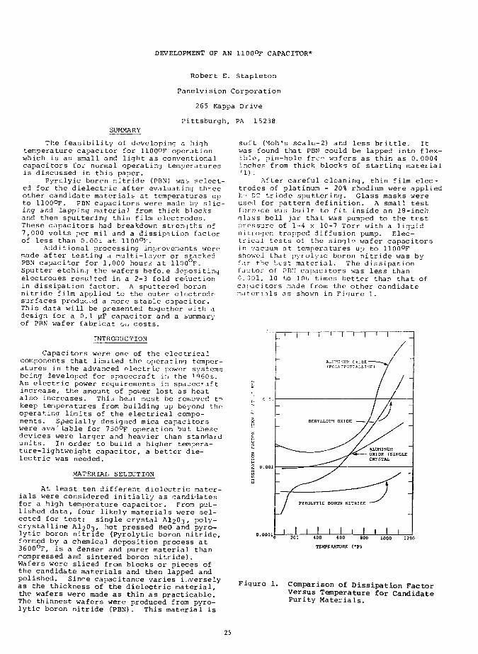
DEVELOPMENT OF AN 1100°F CAPACITOR*
Robert E. S t ap l e ton
Panelvision Corporation
265 Kappa Drive
Pittsburgh, PA 15238SUMMARY
The feasibility of developing a hightemperature capacitor for 1100°F operationwhich is as small and light as conventionalcapacitors for normal operating temperaturesis discussed in this paper.
Pyrclyic borcn nitride (PBN) wab select-ed for the dielectric after evaluating threeother candidate materials at temperatures upto 1100°F. PBN capacitors were made by slic-ing and lapping material from thick blocksand then sputtering thin film electrodes.These capacitors had breakdown strengths of7,000 volts per mil and a dissipation factorof less than 0.001 at 1100°F.
Additional processing improvements weremade after testing a multi-layer or stackedPBN capacitor for 1,000 hour.-: at 1100°F.Sputter etching the wafers befo.e depositingelectrodes resulted in a 2-3 fold reductionin dissipation factor. A sputtered boronnitride film applied to the outer electrodesurfaces produced a more stable capacitor.This data will be presented together with adesign for a 0.1 uF capacitor and a summaryof PBN wafer fabricat on costs.
INTRODUCTION
Capacitors were one of the electricalcomponents that limited the operating temper-atures in the advanced electric power systemsbeing developed for spacecraft in the 1960s.As electric power requirements in spacecraftincrease, the amount of power lost as heatalso increases. Thij heat must be removed tnkeep temperatures from building up beyond theoperatina limits of the electrical compo-nents. Specially designed mica capacitorswere available for 750°F operation but thesedevices were larger and heavier than standardunits. In order to build a higher tempera-ture-lightweight capacitor, a better die-lectric was needed.
MATERIAL SELECTION
At least ten different dielectric mater-ials were considered initially as candidatesfor a high temperature capacitor. From puL-lished data, four likely materials were sel-ected for test: single crystal A1 2O 3, poly-crystalline AI2O3, hot pressed BeO and pyro-lytic boron nitride (Pyrolytic boron nitride,formed by a chemical deposition process at3600°F, is a denser and purer material thancompressed and sintered boron nitride).Wafers were sliced from blocks or pieces ofthe candidate materials and then lapped andpolished. Sinr~e capacitance varies inverselyas the thickness of the dielectric material,the wafers were made as thin as practicable.The thinnest wafers were produced from pyro-lytic boron nitride (PBN). This material is
soft (Moh's scalf-2) and less brittle. Itwas found that PBN could be lapped into flex-ible, pin-hole frc? wafers as thin as 0.0004inches from thick blocks of starting material(1) .
After careful cleaning, thin film elec-trodes of platinum - 20% rhodium were appliedt" DC triode sputtering. Glass masks wereused for pattern definition. A small testfurmce was built to fit inside an 18-inchglass bell jar that was pumped to the testpressure of 1-4 x 10⁻⁷ Torr with a liquidnitrogen trapped diffusion pump. Elec-trical tests of the singlo wafer capacitorsin vacuum at temperatures up to 1100°Fshowed that pyrolyic boron nitride was byfar the best material. The dissipationfa-jtor of PB;! capacitors was less than0.301, 10 to 100 times better than that ofcapacitors made from the other candidatematerials as shown in Figure 1.
•-"
7.
':
1£ o.ooi
2
-
-
J
1 ' i '
BERYLLIt'M
— ^
— ' " ^
I
OXIDE
y
/
PYP.OLYT1C BORON KIT
1 1 1 I 1 1
1
„
—-
. -RIDE
|
1 I ' _
7/"// :ALUMINUMOXIDE (SINGLECRVSTAL
j -
i i i0 200 400 600 BOO 1000 1200
TEMPERATURE IT)
Figure 1. Comparison of Dissipation FactorVersus Temperature for CandidatePurity Materials.
25
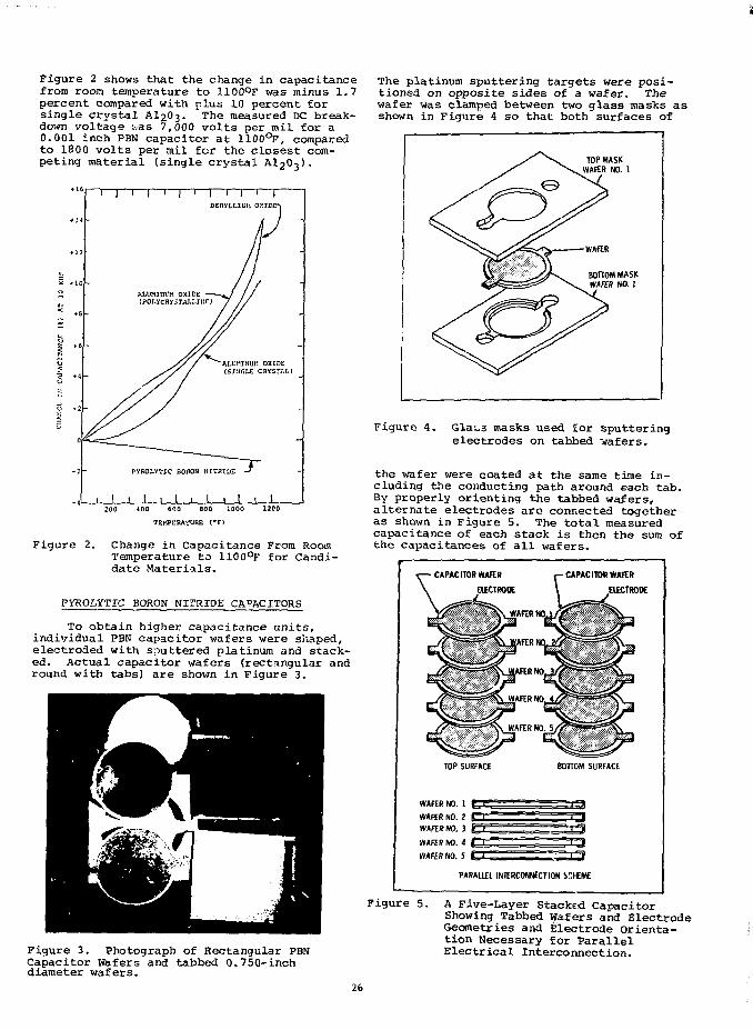
Figure 2 shows that the change in capacitancefrom room temperature to 1100°F was minus 1.7percent compared with plus 10 percent forsingle crystal AI2O3. The measured DC break-down voltage ;vas 7,000 volts per rail for a0.001 inch PBN capacitor at 1100°F, comparedto 1800 volts per mil for the closest com-peting material (single crystal A1 2O 3).
The platinum sputtering targets were posi-tioned on opposite sides of a wafer. Thewafer was clamped between two glass masks asshown in Figure 4 so that both surfaces of
PYROLYTIC BOBOH NITRIDE
I I I I I I 1 1 I I I I
Figure 4. Glats masks used for sputteringelectrodes on tabbed "vafers.
200 400 600 800 1000 1200
TEMPERATURE t#F)
Figure 2. Change in Capacitance From RoomTemperature to 1100°F for Candi-date Materials.
PYROLYTIC BORON NITRIDE CAPACITORS
To obtain higher capacitance units,individual PBN capacitor wafers were shaped,electroded with sputtered platinum and stack-ed. Actual capacitor wafers (rectangular andround with tabs) are shown in Figure 3.
the wafer were coated at the same time in-cluding the conducting path around each tab.By properly orienting the tabbed wafers,alternate electrodes are connected togetheras shown in Figure 5. The total measuredcapacitance of each stack is then the sum ofthe capacitances of all wafers.
CAPACITOR WAFER
HJECTROK
TOP SURFACE BOTTOM SURFACE
WAFER NO. 1 C E
WAFER NO. I C C
WAFER NO. 3 g E
WAFER NO. 4 f ^ T "
WAFER NO. 5 C E
PARALUL INTERCONNECTION SHHEME
Figure 3. Photograph of Rectangular PBNCapacitor Wafers and tabbed 0.750-inchdiameter wafers.
Figure 5. A Five-Layer Stacked CapacitorShowing Tabbed Wafers and ElectrodeGeometries and Electrode orienta-tion Necessary for ParallelElectrical Interconnection.
26
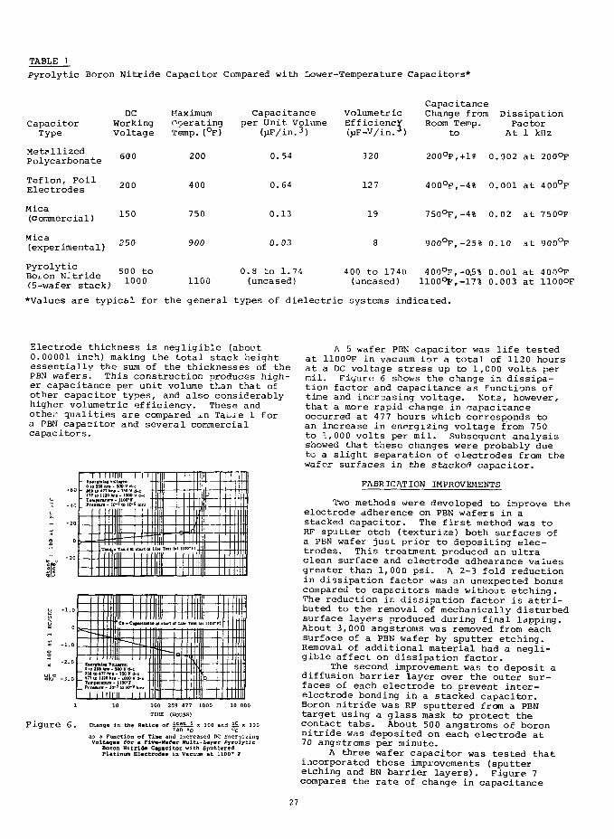
TABLE 1Pyrolytic Boron Ni t r ide Capacitor Compared with iKJwer-Temperature Capacitors*
CapacitorType
MetallizedPolycarbonate
Teflon, Foi lElectrodes
Mica(commercial)
Mica(experimental)
Pyrolyt icBoi.on NJ.tr idef5-wafer stack)
DCWorkingVoltage
600
200
150
250
500 to1000
MaximumOperatingTemp. (°F)
200
400
750
900
1100
Capacitanceper Unit Volume
(uF/in.3)
0. 54
0.64
0.13
0.03
0.8 to 1.74(uncased)
VolumetricEfficiency(jiF-V/in.3)
320
127
19
CapacitanceChange fromRoom Tepip.
to
200°F,+l% 0.
400°F,-4% 0.
750°F,-4% 0.
DissipationFactor
At 1 kHz
002 at 200°F
001 at 4 00°F
02 at 750°F
900°F,-25% 0.10 at 900°F
400 to 1740 400°F,-0.5% 0.(uncased) 1100°F,-17% 0.
001 at 4 00°F003 at 1100OF
*Values are typical for the general types of dielectric systems indicated.
Electrode thickness is negligible (about0.00001 inch) making the total stack heightessentially the sum of the thicknesses of thePBN wafers. This construction produces high-er capacitance per unit volume than that ofother capacitor types, and also considerablyhigher volumetric efficiency. These andother qualities are compared ±n Tauie 1 fora PBN capacitor and several commercialcapacitors.
TIME (HOURS)
F i g u r e 6. Change 171 the Rat:
as a Function of Tine and Increased DC EnergizingVoltages for a Five-Wafer Multi-Layer pyrolytic
Boron Nitride Capacitor wi th SputteredPlatinun Electrodes in Vacuum at 1100* F
A 5 wafer PBN capacitor was life testedat 1100°F in vacuum lor a total of 1120 hoursat a DC voltage stress up to l,C00 volts permil. Figure 6 shows the change in dissipa-tion factor and capacitance as functions oftime and increasing voltage. Note, however,that a more rapid change in capacitanceoccurred at 4 77 hours which corresponds toan increase in energizing voltage from 750to 1,000 volts per mil. Subsequent analysisshowed that these changes were probably dueto a slight separation of electrodes from thewafer surfaces in the stacked capacitor.
FABRICATION IMPROVEMENTS
Two methods were developed to improve theelectrode adherence on PBN wafers in astacked capacitor. The first method was toRF sputter etch (texturiza) both surfaces ofa PBN wafer just prior to depositing elec-trodes. This treatment produced an ultraclean surface and electrode adhearance valuesgreater than 1,000 psi. A 2-3 fold reductionin dissipation factor was an unexpected bonuscompared to capacitors mads without etching.The reduction in dissipation factor is attri-buted to the removal of mechanically disturbedsurface layers produced during final lapping.About 3,000 angstroms was removed from eachsurface of a PBN wafer by sputter etching.Removal of additional material had a negli-gible affect on dissipation factor.
The second improvement was to deposit adiffusion barrier layer over the outer sur-faces of each electrode to prevent inter-electrode bonding in a stacked capacitor.Boron nitride was RF sputtered from a PBNtarget using a glass mask to protect thecontact tabs. About 500 angstroms of boronnitride was deposited on each electrode at70 angstroms per minute.
A three wafer capacitor was tested thatincorporated these improvements (sputteretching and BN barrier layers). Figure 7compares the rate of change in capacitance
27
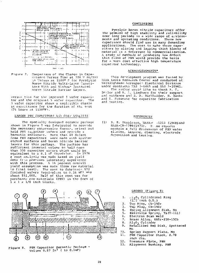
Figure 7. Comparison of the Change in Capa-citance Versus Time at 500 V dc/Milin Vacuum at 1100° F for PyrolyticBoron Nitride Multi-Layer Capaci-tors With and Without SputteredBoron Nitride Barrier Layer;;.
versus tirr.e for the improved 3 wafer capaci-tor and the original 5 wafer capacitor. The3 wafer capacitor shows a negligible changein capacitance for the duration of the test(75 hours at 1100°F).
LARGER PBN CAPACITORS AND COST ANALYSIS
The specially designed ceramic packageshown in Figure 9 was fabricated to providethe necessary compressive forcer, orient andhold PB?; capacitor wafers and provide ahermetic enclosure. More thar. 40 defectfree PBN capacitors were made with sputteretched surfaces and boron nitride barrierlayers for this package. The package hassufficient internal volume to "hold morethan 300 capacitor wafers which would beequivalent to a 0.1 uF capacitor. In 1976a cost analysis was made based on yielddata fri.n previous laboratory experiencewith this process. A 16 percent overallyield assumption was made (from raw material(-.o final test). The cost to fabricate 572finished wafers (equivalent to 0.16 uF) wasabout $51,000. Half of this cost was forpurchasej raw materials (PBN) in the form of1 x 1 x 1/8 inch blocks.
CONCLUSIONS
Pyrolyic boron nitride capacitors offerthe promise of high stability and reliabilityover long periods in a wide range of ej.viron-ments and operating conditions. These newcapacitors should find use in many demandingapplications. The cost to make these capa-citors by slicing asid lapping thick blocks ofmaterial is a deterrent to commercialization.A study of methods of producing low defectthin films of PBN would provide the basisfor a more cost effective high temperaturecapacitor technology.
AC KNO'.v LEDGM ENTS*
This de-'elopment program was fur.aed byNASA Lewis Research Center and conducted atWec-tir.ghouse Aerospace Electrical Divisionunder contracts MAS 3-6465 and MAS 3-10941.
The author would like to thank A. C.Beiler and P.. .".. Lindberg for their supportand guidance ant' S. D. Burkholder, H. Banksand f\. Schumate for capacitor fabricationand testing.
REFERENCES
(1) R. E. Stapltton, :jASA-f -1213 (1968)andNASA-CR-1799U971). T. .se reportscontain a full discussion of PBN waferslicing, lapping, cleaning, electrodedeposition and testing.
LEGEND (Figure 8)
Figure 8. PBN Capacitor Hermetic Package -Volume 0.37 In^ { to O.luF)
1. ••J-2°3 Cylindrical- Ring(1.5 inch O.D. )
2. Top Ring, Cb-l%Zr3. Top Plug, Cb-l%Zr4. Spring Alignment disk. Ho5. Be l lv i l l e Spring, Ta(T-ll l)6. Electron Beam Weld7. Braze Alloy, 60Zr-25V-15Cb8. Al2°3 Cylinder9. Metallized Beo Disk, Sputtered
Mo30. Spring Support Pla te , Mo11. PBN Capacitor Stack, 0.78
inch dia .12. Pressure P la te , PBN13. Alignment Bushing, PBN
28
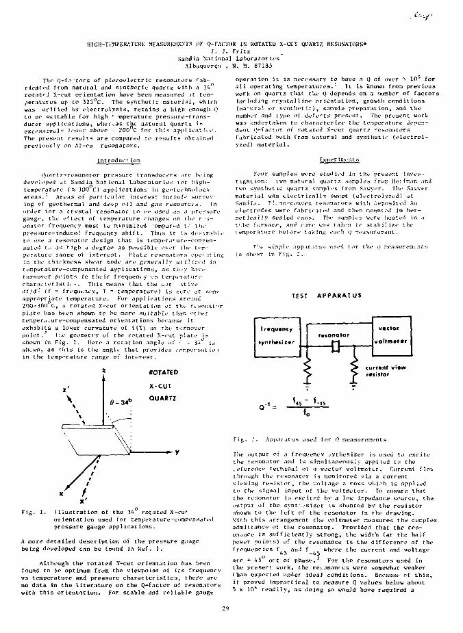
HIGH-TtMPERATURE MEASUREMENTS OF Q-FACTOR IK ROTATED X-CUT QUARTZ RKSOSATORS*
I. J. Fritz
Sandia National Laboratories
Albuquerqu , N, M. 87135
The Q-fo tors of pievoelectric resonators fab-
ricated from natural and synthetic quartz with a 34
rotateJ X-cut orientat ion have been measured -it tem-
peratures up to 325°C. The synthet ic material, vhich
was •urified by electrolysis, retains a high enough Q
to be suitable for high ' -mperature pressure-trans-
ducer appl icat ions, whereas the aatural quartz ***
excessively lossy above "- 200 C for this appl icat Uu1 .
The present result's are compared to results obtained
previously on AT-cu resonators.
Int, roduc *" ion
thiartz--resonator pressure transducers are be inpdeveloped ^t Sandia National Laboratories tor hifch-temperaturc (sr 300 C) applications in geotechnolav;yareas.1 Areas of particular interest inc lud<* surviv-ing of geo thermal and detp oil and gas resource .s. f norder tor a crystal resonator to nt* used as n pressuregauge% tru- ef t ect of temperature changes on t ho r s-onator frequency must he dUiioized *o*3-par*>ti to thepressure- induced frequency shif t . Thus it is d«-s iraM *.-to use a resonator design that is tempera •"ure-i-onpen-sated [ u as high a degree as poss ible over t lie u-rn-perature range of interest . J'lsle resonators ope- it in-,;in the thickness shear node are generally ut il izud intemper a ture-conipensated apf 1 icat ions , as t JK'V tuvcturnover points in tliuir frequent >" vs ter.pt?ratnrvcharac Ler ist it -". This means tliat the uor itivedf/d"" (f = frequency, T * temperature) is zero at son*.*appropriatf temperature. For applications around200-500 C, a rotated X-cut orientation of the resonatorplate has been shown to he more suitable than otrvrtempera-ure-compensated or ientat ions because i texhibits a lower curvature of f (T) ai t he ti:moverpoint. ^ 1 i.e geometry of the rotated X-cut pint e i shown in Fig. 1. Here a rotation angle of -~ = i-1 isshewn, as thin is the angIt* that provides conpersat io tin the temperature range of interest .
ROTATED
Fig. 1. Illustration of the 34 rotated X-cur
orientat ion used for temperature-comnensateJ
pressure gauge applications.
A more detailed description of the pressure gfiuge
being developed can be round in Ref. 1.
Although the rotated X-cut orientat ion has been
found to be optimum from the viewpoint of its frequency
vs temperature and pressure characteristics, there are
no data in the literature on che Q-factor of resonators
with this orientation. For stable and reliable gauge
operation in is necessary to have a Q of over ^ 10 s for
all operating temperatures.1 It is known frora previous
work on quartz that die Q depends on a number of factors
including crystall ine or ion tat. ion, grovsh conti it ions
(na'urn! or synthft ic), sample preparat ion, and the
number and type of def^rts present. The present work
was undertaken to characterize Die temperature depen-
dent Q-factor of rotated X-cut quartz resonators
fabricated both from natural and synthetic (electrol-
yzed) material.
Four samples wen? stud it?d in t he present inves-
tigation: L W O natural quarts ^anples frtm Hoff".in and
two synthtt IC quartz sanpl <ls f ran Sawyer. The SIIWV*T
material was electrically swept (e,lfctro3yzi*d) .it
Sand i.i. V '. TO-convex resonator s with deposited Au
eiectfodes were fabricated and then r.ountec in her-
met ica 11 y sealed cans. The s;inp! cs were beaten in ;i
t'.be furnace, and euro was f afcen to stab; ] i?.o t he
temperature before taking each ',"> neasurenunt.
s inpl t- ;ipp3
in Hi j;. 2.
L.its
TEST APPARATUS
Irvquancy
>ynth«siz«rresonator
•a-
vactor
volrm*r*r
currant viaraiittor
Kig. J. App.ir.it M S used for Q nt*asuren«*nts
The output of a frequency i-ythesizer is used to excite
the resonator and is simultaneous]y applied to the
;efcrence tvrminal of a vector voltraetcr. Current flov
through the resonator is wonitoreci via a current
viewing resistor, the voltage r. ross which is applied
to the signal input of the voltmeter. To ensure that
the resonator i s exc ited by a low impedance source, the
ontput of the synt.-jsizer is shunted by the resistor
shown to the left of the resonator in the drawing.
\'ich this arrangement the voltmeter measures the complex
admittance of the resonator. Provided that the res-
onance is suf f ic ient1y strong, the width (at the half
power noinrs) of the resonance is the difference of the
frequencies f and f where the current and voltage
are + 45 ot-c ot phase.3 For the resonators used in
the preser? work, the re^jnanccs were somewhat weaVer
than expected under ideal conditions. Because of this,
it proved impractical to measure Q values below about
5 x 101* readily, as doing so would have required a
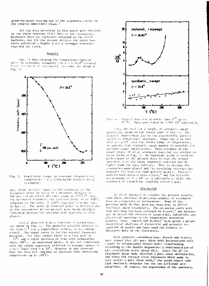
point-by-point crac ing out oi the resonance c i r c l e inthe complex admittance p l ane . 1
All the data nreHentt-d in this paper were o b t i i : wat the th i rd overtone (: = 1 MHz) of the rcsimaivri . .Resonator data arc t yp i ca l l y obtained a t the \ i t t hharmonic, but for the present devices the th i rd har-tnon ic ex hi bitud a higher Q ar<d a stronger rt 'srn;inrcthan did the f i f t h .
Resul ts
Typ „ -1 data showing the temperature- iivlu* edshi' t in n-sonanrL' frequency * or a " = ^i .0° rn t .n e jX-^-ii: •*i- > ::.-t! or a: it:tios;iher i ;iri ^•;uri- ire sbovn irFig. 3.
1M 299 310
f i g . 3. Krairt ion.il rhan^e in resonant ir**q»enrv v s .tercperaiur.- : >r a (font oured > rot at i-d X-* utr e s o n a r n r .
M s , shown in ; hi-> t i ^ i - i s ivK. i ^ n i t u J e .-: : hetn-quem y s u i t ; pr vUu'ed \-v .i p r e s s u r e unri-. iM' o!inn p s i Mr ;i» .u-tu.il pr. ssuri- .i.supe .it J7> r . 1 fVrthe ri.-sm.itor r,..'.isuvf.l. t he tur::*'ver f o in ; i-, ,it iOO°t ,con pared i f t he v.i !»*• <>: J2H* ( t-:<pt*t t i'J i r>r. t h»- J .u. iin Ret . 2. The sh i t t in turm-VL-r poini is hrI it-ved dueto t lie r e s o n a t o r s in t he prefer. : work bv inr, si it-.ht 1 vcontimr ed WJUTIMS tlu- prev Litus work per T..J i ns to fJ.itp l a t e s .
. Vp it**i ] d.it.j t or i] an a t urut ion »i t enper. i iuri-arc ahovn in K ig . '*. Tliu quani i t v ac t\ia 11 v ;>1 ot t e i i sthe l o s s i.| 5 (on a Ioj;ar i thn ic sr.U . • ) , as i s < i-nven-t i o n a l . The upper curve i s for t he t u t tiro I (unsvept )m i t e r i . i l . For t h i s sanp le t he re i s n l o s s pea*: ,it
70 C and a rap id i n c r e a s e of l o s s with tempera tureabitve JOO°C. A.s a^nt iom>t3 above , i t was not •jonveniemwith t he s i n p l t ' a p p a r a t u s u t i l i s e d to nea su re vah iv s or«.i r:u-'fi lover t han 5 x 10**. Hrwever i t was observedthat the l o s s d vi i onl inui> to i nc r ea se v i t h im:rensin£t e n p e r a t u r e up tu jOO C.
21
tl
natural, «-nswept
0 - 34.15°
synthetic, swept
0 - 34.1°
IN M 3M
Tvpii.iJ J.jLn f or ac nist ic l o s s *J
;.hn-*Ti in i ho
harrA-nu->.
T'-w
t-.j!ior: ;s i rr t-.i i .1: t-i v apparent. Sinco t\\<- \) is ~f*rv:hin J . T :< 10 ovi-r t;uj o:u irt- rango 01 tv'^p^raturi t
i* appL-.ir^ :L,tt s'Til hvl h- svupt quartz i s .s'jitnhlt- lorprcssuri' e.n:^o aprl icat itm^. Hata obtained (Ti theother ; .pW> of s'--_ pr svnthetic material are siir-ilar tolliose shouTi jn Fit;. '.. An tnportaTU point tc r;e:^t ionwith rep.-irii Co the present data is tii.it the .irtua]ir i l r insu t> d the swept ^vmthetir rznteria1. r^iv he(•ii;!ier t h.in the data indicate. This is in-causr t he• L-s<>nators vere plated anil M-.e res i s t ing s t resses r?.av.iomnatu- the loss i or hich qu.iiitv quart, ' . I'revio-.sworkers have not iied th i s c r t e c t , " a:id for r e i i ab l ir.e.isu-enient s o: t> > ! 0* it :s ndvisnhle to drivt.- t heresonator !>•• capai-it ivr coup] ir.fi across a gap.
i)ist ussinn
H is o: interest to rur.pare t he present r e su l t svi th those obtained in previous studies nf resonatorloss as ,] 'unit ion 01 ternera ture . Most of theprevious wrrk in thir. area has been done on AT-eutthirkiu'ss shear resonators. The exiensive early workthat was Jtxie lias been reviewed by Frascr," who discus-ses in Jvt.jil t!w e f i e t t s oi impurit ies, radia t ion, andeKvtrii-.il sweeping en the temperature dependent,-notisti.- los-s. N'nwick and Stanley5 h.tvc given a group-theoretic-a! ana'vsi.s of d i e l ec t r i c and acoustic n -laxat ion in quarts and have used tht> resu l t s ;ointerpret data in the l i t e r a t u r e .
Fron syrsii-try ronsidcr.it ions, Nowic'n and Stanleyhave argued thai a l l pure shear node defornations willcouple to rel.ixational noraal icode^ transforoingaccording, to the doubly degenerate E representation ofthe c rvs ta l l ine point group ( » ; ) . Since the AT-cutthickness shear node involves a pure shear defornacion,and since the rotated X-cut thickness shear mode isvery nearly a pure shear node , ' one would expect sira-i la r .inelastic behavior for the two different o r i -en ta t ions . Of course, the magnitudes ot the Jne las t ic
30
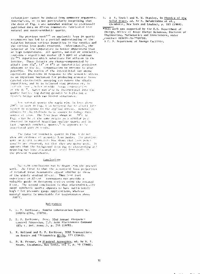
relaxatioir= cannot be deduced from symmetry argument s.
Nonet he1 t?ss, it is not part icularlv snrpr iz ing that
the data of Fig. 4 are somewhat similar to previously
publ ished data on AT-cut resonators f abr K-.-it ed I rom
natura 1 and swept -synthet ic- quarts .
The prev ious work1* * * on ane List ic loss in quartz
resonators has led tn a part ial understand ing of t he
relaE ion between var iou.s impur i t ies in the &az)pl es and
the various loss peaks observed. i/nf ortunatel\ , the
behav ior at low temperatjre is bet ter understood t han
at high temperature. Al 1 quartz, nat.iral or synthet ic,
eonta ins .» sign it if ant njmber (> S ppm) of al uminum
(A > 3 +) impur it ies wh ich ;ubst itute for si 1 icon in tin.
lattice. These detects .ire charge-compensated by
a I kal l ions ('."a , I. i or K +) .it interst:t ial pox i t ion a
ad iacent to Che A« . Compensat ion by protons i s also
possible. The mot ion of the interst itial ion among
equ iva1eni pos i t ions in response to t he aeon stir stress
i s an import ant mechanism lor produc ing a c oust ic 1 oss.
Caref u 1 elee t rolyt ie sweep ing can remove t he al k.i 1 i
impur it ies, and it is be 1 ieved t iiat protons *.*r» i''
5. A S. NowiLk and M. W. Stanley, in Physics of the
Sol id State, ed. by S. Balakrishna et al.,
(Academic, New York and London), p. 183 (1969).
*This work was supported by the U.S. Department ofEnergy, Office of Basic Energy Sciences, Division ofEngineer ing, Mathemat ics and Geosc iences, under
contract I>EAf:OW6-P"00789.A t*. S. Department of Energy facility.
L»I t he A • . Wat e r may a 1 so In- i n c o r p o r a t ed i n t o t;it-q u a r t / l a t t i c e ( eg J u r ing growt h ) bv r e p l a c i ni; a^ i - o - < : b r i d g e w i t h two S i-O-H s t rue t u r e s .
for nat u r . i l q u a r t 7. t h e r a p id r i s i in 1 o.ss aS>vt-200 ( is s e e n in r i g . U i s be 1 i eved due t o a i ka] i .1 i f -I u s ion in f t s p o n s e t n t i;e a p p " i e d s t r e s s . Kemi'va ! o:a l k a l i s bv , l e c t r . ' l v s i s i s m e s s a r v t o r e d u c e t h i sSOUTL e i>: l o s s . The l o s s peak shown a t 70 ( inYi£. '* m.iv he of tlu- s ane o r i g i n a s ;* s i m i l a r pe.i llib se t ved in na t u r a 1 h r a z i 1 i an op.i! i;n- q u a r t / ami in* a s t , - g r o u t h s v n t bet ii quar t 7 . ** It a p p e a r s t i* bea s s o e i a t ed w i t h i>H b . i n d s .
fhe Li.it .i ' i»r *-vnt be t IL q u a r t z in Yip,. •'• do notshow anv ev idenc*- o\ .a: o u s t ic l o s s p e a k s . The- pr ev i.iu "•worl on AT - CMt r e ; n n . i : « r s h.is ^};ov:! * hat ] ,'S1- pen , -iusu.i 1 1 v a r e o b s e r v e d , but t i n t t he v a r e qu i t e weak . I ta p p e a r s t ha t t he b a c k g r o u n d l o s s due t o e 1 ec t rod jng ai. '.mount ing n a v 'nave ol S i u r e d rfi-v ^n U ! i i ' ^ s iu-aF-. i rt h e p r e s e n t measurement s .
Cone I u s i o n s
TwLt m.-iin c o n c l u s i o n s nav be drawn , ' o n t h e p r e s e n tw o r k . i he f i r s t i s t h a t t l i e a c o u s t i c a l l o s s p r o p e r t i e sot" r o t at ed X-cut r e s o n a t o r s a p p e a r s i n i l a r t o t h o s eof t h e w i d e l y s t u d i e d AT-*, t i t . Thus r .os t p a s te x p e r i e n c e on AT ->. ut r e s o n a t o r s r.ay p r o / i d e av a l u a b l e g u i d e in d e s i g n i n g d e v i c e s u s i n g t h e r o t a t e dX - c u t . The s econd cone I u s ion i s t h a t e l e c t r o l v t i c a I ! vswept s y n t h e t i c q u a r t z a p p e a r s t o have s u f f i c i e n t l vh i g h «.) f o r p r e s s u r e g a u g e a p p l i c a t i o n s , w h e r e a sn a t u r a 1 q u a r t s i s u n s u i t a b l e for t e m p e r a t u r e s above
2OlVY.
Kef
1. K . P . KerN i s.se , Sand ia Laborator ies Report No .
SAND7tt-2264, (1979).
2. E. f. EerSisse, Proc. 32nd Annual Froquency
Control Symposium, U.S. Army Electronics Command
(Ele t. Ind. A s s o c ) , p. 25^ (1978).
3. R. Holland and E. P. EerNisse, IEEE Transactions
on Sonicb and 'Urasonics SU-16, 171 (1969).
t*. I). B. Fraser, in PI ysical Acoustics, ed. by W. P.
Mason, (Academic, New York), vol V, p. S9 (1968).
31
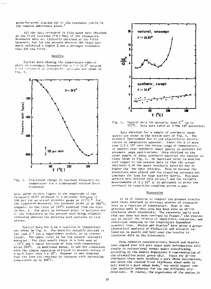
point-by-point tracing out of the resonance circle inthe complex admittance plane.3
All the data presented in this paper were obtainedat the third overtone (fe3 MHz) of the resonators.Resonator data are typically obtained at the fifthharmonic, but for the present devices the third har-monic exhibited a higher Q and a stronger resonancethan did the fifth.
Results
Typical data showing the temperature-inducedshift in resonance frequency for a •'' = 34.0° rotatedX-rut rt-soiiatnr at jtmosphtT i> pru-ssure aru shown inFig. 3.
u
-200
-400
-600
-too
\
\
\
| 100 psi
9=34.0°
-
shifl \ ,
* * " 1100 200 300
i g 3. Fractional change in resonant frequency vs.temperature for a (contoured) rotated X-eutresonator .
Also shown in tiny figure is the magnitude of thefrequency shift produced by a pressure increase of100 psi for an actual pressure gauge at 275°C.* Furthe resonator measured, the turnover point is at 300 C,compare! to the value of 220 C expected from the datain Ret . 2. The shi f t in turnover po int. is bel ieved dueto t!ie resonators in the present work be ing FIightlycontoured whereas the prev ious work pertains to flatplates.
Typical data for Q as a function of temperatureare shown in Pig, A. The quantity actually plotted isthe ioss Q 1 (on a logarithmic scale), as is conven-tional. The upper curve is for the natural (unswept)material. For this sample there is a loss peak at^ 70 C and a rapid increase of loss with temperatureabove 200°C. As mentioned above, it was not convenientwith the simple apparatus utilized to measure values ofQ much lower than 5 x 101*. However it was observedthat the loss did continue to increase with increasingtemperature up to 300 C.
21
10
natural, unswept
0 = 34.15°
synthetic, swept
0 = 34.0°
2M 311
Fig. 4. Typical da'a for acoustic loss Q up to325°C. Data were taken at 3 MHz (3d harmonic).
Data obtained for a sample of synthetic sweptquartz are shown in the bottom part of Fig. 4. Thedramatic improvement due to the electrolytic purifi-cation is immediately apparent. Since the Q is morethan 2.5 x 10s over the entire range of temperature,it appears that synthetic swept quartz is suitable forpressure ,auge applications. Data obtained on theother sample of swept synthetic material are similar tothose shown in Fig. 4. An important point to mentionwith regard to the present data is that the actualintrinsic Q of the swept synthetic material may behigher tha the data indicate. This is because theresonators were plated and the resulting stresses maydominate the loss for high quality quartz. Previousworkers have noticed this effect,1" and for reliablemeasurements of Q > 106 it is advisable to drive theresonator by capacitive coupling across a gap.
Discussion
It is of interest to compare the present resultswith those obtained in previous studies of resonatorloss as a function of temperature. Most of theprevious work in this area has been done on AT-cutthickness shear resonators. The extensive early workthat was done has been reviewed by Fraser,* who discus-ses in detail the effects of impurities, radiation, andelectrical sweeping on the temperature dependentacoustic loss. Nowick and Stanley5 have given a group-theoretical analysis of dielectric and acoustic re-laxation in quartz and have used the results tointerpret data in the literature.
From symmetry considerations, Nowick and Stanleyhave argued that all pure shear mode deformations willcouple to relaxational normal modes transformingaccording to the doubly degenerate E representation ofthe crystalline point group (D3). Since the AT-cutthickness shear mode involves a pure shear deformation,and since the rotated X-cut thickness shear mode isvery nearly a pure shear mode,2 one would expect sim-ilar anelastic behavior for Che two different ori-entations. Of course, the magnitudes of the anelas.ic
30
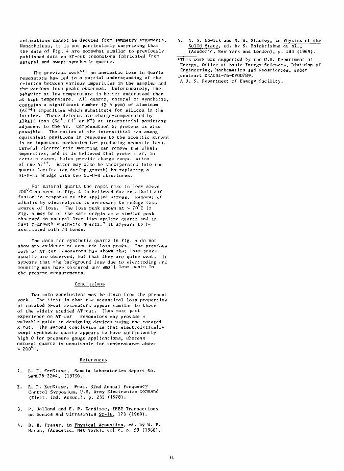
relaxations cannot be deduced from symmetry arguments.Nonetheless, it is not particularly surprizing thatthe data of Fig. A are somewhat similar to previouslypublished data on AT-cut resonators fabricated fromnatural and swept-synthetic quartz.
The previous work1*'5 on anelastic loss in quartzresonators has led to a partial understanding of therelation between various impurities in the samples andthe various loss peaks observed. Unfortunately, thebehavior at low temperature is better understood thanat high temperature. All quartz, natural or synthetic,contains a significant number (> 5 ppm) of aluminum(A£3+) impurities which substitute for silicon in thelattice. These defects are charge-compensated byalkali ions (Na+, Li+ or K+) at interstitial positions-adjacent to the A£. Compensation by protons is alsopossible. The motion of the interstitial ie-n amongequivalent posit ions in response to the acouitic stressis an important mechanism for producing acoustic loss.Careful elect rolyt ic sweeping can remove the alkaliimpurities, and it is believed that protons or, incertain rapes, holes provide charge compei ;atinnof the A>3+. Water may also be incorporated into thequartz iattice (eg during growth) by replacing aSl-O-Si bridge with two Si-O-H structures.
For natural quartz the rapid rise in loss above200 C as seen in Fig. U is believed due to alkal i d i f —fus ion in response to the applied stress. Remova1 ofalkalis by electrolysis is necessary to reduce thissource of loss. The loss peak shown at "^ 70 C inFig. 4 may be of the same origin as a similar peakobserved in natural Braz i1ian opaline quart z and infast z-growth synthet ic quartz. ** It appears to beasst-iated with OH bonds.
The data for synthetic quartz in Fig. U do notshow any evidence of acoustic loss peaks. The previous-work on AT-cut resonators has shown that loss penksusually are observed, but that they are quite weak. Itappears that the background loss due to eleftroding andmount ing mav have obscured any smaII loss peaks inthe present measurements.
Conclusions
Two main conclusions may be drauTi from the presentwork. The first is that t'ue acoustical loss propertiesof rotated X-cut resonators appear similar to thoseof the widely studied AT-cut. Thus most pastexperience on AT-cut resonators may provide avaluable guide in designing devices using the rotatedX-cut. The second conclusion is that electrolyticallyswept synthetic quartz appears to have sufficientlyhigh Q for pressure gauge applications, whereasnatural quartz is unsuitable for temperatures above^ 200°C.
References
1. E. P. EerNisse , Sandia Laboratories Report No.SAND78-2264, (1979).
2. E. P. EerNisse, Proc. 32nd Annual FrequencyControl Symposium, U.S. Army Electronics Command(Elect. Ind. Assoc), p. 255 (1978).
3. P. Holland and E. P. EerNisse, IEEE Transactionson Sonics and Ultrasonics SU-16, 173 (1969).
4. D. B. Fraser, in Physical Acoustics, ed. by W. P.Mason, (Academic, New York), vol V, p. 59 (1968).
5. A. S. Nowick and M. U. Stanley, in Physics of theSolid State, ed. by S. Balakrishna et al.t(Academic, New YorK and London), p. 183 (1969).
*This work was supported hy the U.S. Department ofEnergy, Office of Basic Energy Sciences, Division ofEngineering, Mathemat ics and Geosc iences, under^contract DEAC04-76-DP00789.A U. S. Department of Energy facility.
31

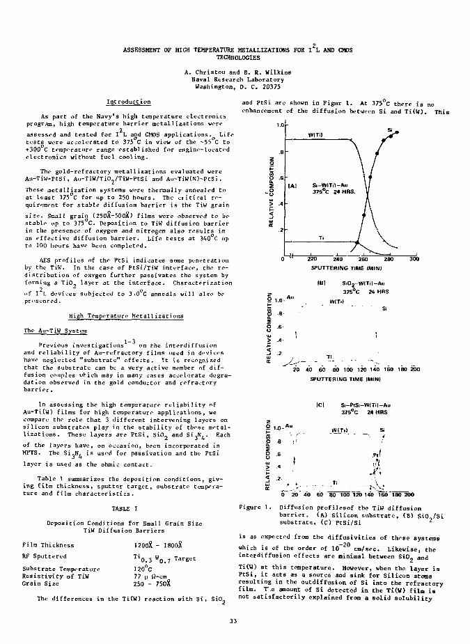
ASSESSMENT OF HIGH TEMPERATURE METALLIZATIONS FOR I L AND CMOS
TECHNOLOGIES
A. Christou and B. R. Wilkins
Naval Research Laboratory
Washington, D. C. 20375
pro
Introduct ion
As part of the Navy's high temperature electronics>gram, high temperature barrier metallizations were
assessed and tested for I L and CMOS applications. Life
tests were accelerated to 375 C in view of the -55 C to
+300 C temperature range established for engine-located
electronics without fuel cooling.
The gold-refractory metallizations evaluated were
Au-TiW-PtSi, Au-TiW/TiO2/TiW-PtSi and Au-TiW(N)-PtSi.
These metallization systems were thermally annealed to
at least 375 C for up to 250 hours. The critical re-
quirement for stable diffusion barrier is the TiW grain
size. Small grain (25OA-5OOA) films were observed to be
stable up to 375 C. Deposition to TiW diffusion barrier
in the presence of oxygen and nitrogen also results in
an effective diffusion barrier. Life tests at 340 C up
to 100 hours have been completed.
AES profiles of the PtSi indicates some penetration
by the TiW. In the case of PtSi/TiW interface, the re-
distribution of oxvgen further passivates the system by
forming a TiO layer at the interface. Characterization9
of I L devices subjected to 3t0 C anneals will also bepresented.
High Temperature Metall izations
and PtSi are shown in Figur 1. At 375°C there is no
enhancement of the diffusion between Si and Ti(W). This
WITi)
o
a .6
"OUJ> .4
.2 -
Si-VD|Ti)-Au375°C 24 HRS.
Z2O 240 260 300
SPUTTERING TIME IMIN)
[Bl SiOz-W(Til-Au375°C 24 HRS
WITil
O 8
The Au-TiW System
1-3Previous investigations* J on the interdiffusion
and reliability of Au-refractory films used in devices
have neglected "substrate" effects. It is recognized
that the substrate can be a very active member of dif-
fusion couples urich may in many cases accelerate degra-
dation observed in the gold conductor and refractory
barrier.
20 40 60 80 100 120 140 160 180 200SPUTTERING TIME (MINI
In assessing the high temperature reliability of
Au-Ti(W) films for high temperature applications, we
compare the role that 3 different intervening layers on
silicon substrates play in the stability of these metal-
lizations. These layers are PtSi, SiO and Si-.N,. Each
of the layers have, on occasion, been incorporated in
MPTS. The Si,N, is used for passivation and the PtSi
layer is used as the ohmic contact.
Table I summarizes the deposition conditions, giv-ing film thickness, sputter target, substrate tempera-ture and film characteristics.
TABLE I
Deposition Conditions for Small Grain Size
TiW Diffusion Barriers
ICl
Film Thickness
RF Sputtered
Substrate TemperatureResistivity of TiWGrain Size
1200S - 1800X
T i0.3 W0.7 T a r 8 c t
120°C
77 v Si-cm
250 - 75OA*
Si-PtSi-W(Til-Au375°C 24 HRS
2 1.0~M
55 '
I .8-8 -6> * •
2 •*•UJ *
mm)
,P.f
The differences in the Ti(W) reaction with Si, SiO,
0 20 40 60 80 100 120 140 160 180 200
Figure 1. Diffusion profilesof the TiW diffusion
barrier. (A) Silicon substrate, (B) SiO /Sisubstrate, (c) PtSi/Si
is as expected from the diffusivities of these systems
which is of the order of 10~ cm/sec. Likewise, the
interdiffusion effects are minimal between SiO, and
Ti(W) at this temperature. However, when the layer is
PtSi, it acts as a source and sink for Silicon atoms
resulting in the outdiffusion of Si into the refractory
film. T e amount of Si detected in the Ti(W) film is
not satisfactorily explained from a solid solubility
33
argument. These results agree with our previous workwith Ta on Si and FtSi and with Sinha's work with WSi-
formation on PtSi-Si substrates. The excess silicon inthe TiW will result in a refractory silicide formationat higher temperatures. Our conclusion, to date, isthat the Au-TiW system with snail grain TiW is stableup to 375°C.
The Oxide/Nitride Assisted Diffusion Barriers
The deposition of TiW in the presence of oxygenoverpressure or nitrogen has been determined to improvethe overall thermal stability of the TiW diffusion bai-
rier. An overpressure of 10 Torr of oxygen or nitro-gen was used in each case resulting in Titanium nitride
4 5passivation of the TiW grain boundaries. ' Since theprimary diffusion mechanism at temperatures below 500 Cis grain boundary diffusion, the formation of TiN atthe TiW grain boundaries inhibits significant grainboundaries up to 450 C. The Au-TiW(TiN)-PtSi systemwas found to be stable up to 450 C as shown in Table II,where the at. % Si and Au detected in the bulk of theTiW by energy dispersive x-ray analysis is summarized.
TABLE II
Evaluation of the TiW(TiN) Diffusion Barrierup to 450°C
Anneal Temperature at. % Si at. % Au(100 hrs) Detected in TiW(TiN)
300 C340°C350°C400°C450°C
However, at 450 C, the significant observation is thatSilicon was not observed in the Au overlayer thus show-ing the overall stability of TiW(TiN) as a diffusionbarrier.
I L Test Elements With Au-TiW Metallizations
As part of the Navy's High Temperature Electronics2
a custom I L metallization test mask set has been pro-cessed using the Au-TiW-PtSi system. The test maskincludes a number of rifferent test elements which areaimed at determining design constraints on ohmic con-tacts, metal width and spacing. Also included are sym-metrical cell I L logic gates and ring oscillators. Theinitial test results look promising in that 2 of 6 (8%)of the oscillators failed within 275 hours. A total ofsix oicillators have now reached 580 hours with nofailures. These tests are continuing and additionalrefinements to the metallization will be incorporated
in the I L devices to be processed in the future.
References
1. J. A. Cunningham, Solid State Elec. jS, 835 (1965).2. J. M. Harris, E. Lugujjo, S. U. Campisano, M. A.
Nicolct and R. Shima, J. Vac. Sci. Technol. 12 (1),524-527 (1978).
3. A. Christou and H. M. Day, J. Appl. Phys. 44 (12),5259-5265 (1973).
4. H. V. Seefeld, H. Cheung, M. Enpaa and M. A.Nicolet, IEEE Trans E.D., Vol. Z£ (4), 873 (1980).
5. M. A. Nicolct, Thin Solid Films, 2, 415 (1978).
ND1.11.82.54.2
ND1.02 .03 .06.5
34
AMORPHOUS r1.. U1IZATI0NS FOR HIGH-TEMPERATURESEHIO • UCTOR DEVICE APPLICATIONS
J. D. WileyECE DepartmentUniversity of WisconsinMadison, HI S3706
J. H. PerepezkoMSME DepartmentUniversity of WisconsinMadison, WI 53706
J. E. NordraanECE DepartmentUniversity of WisconsinMadison, WI 53706
Guo Kang-JinShanghai Inst. Met.Chinese Acad. Sci.Shanghai, China
Abstract - In this paper we present the initialresults of work on a new class of semiconductor metal-izations which appear to hold greet promise as primarymetallizations and diffusion barrier:? for high-temperaature device applications. These metallizations consistof sputter-deposited films of high-Tg amorpl" -rnetalalloys which (primarily because of the absence grainboundaries) exhibit exceptionally good corrosi resis-tance and low diffusion coefficients. Amorpht. j filmsof the alloys Ni-Nb, Ni-Mo, W-si, and Mo-Ei have beendeposited on si, GaAs, GaP, and various insulating sub-strates. The films adhere extremely well to the sub-strates and remain amorphous during thermal cycling toat least 500°C. Rutherford Bacfcscattering {RBS} andAuger F:lectron Spectroscopy (AES) measurements indicateatomic diffussivities in the 10~l9 cm2/S range at450°C.
INTRODUCTION
One of the most difficult problems associated withthe design of semiconductor devices intended for hiqh-temperature operation is that of finding a suitablemetallization system for providing contacts to the semi-conductor. Typical difficulties whicll limit the life-time of semiconductor devices at high temperature in-clude: (1) altered electrical behavior caused by inter-diffusion of metal and semiconductor; (2) dimensionalchanges or embrittlement caused by compound formation,or grain-growth; and (3) catastrophic metallizationfailure due to electromigration. Those must be consid-ered as intrinsic failure modes in the sense that, whilethey may vary in absolute and relative importance fromone system to another, they must always be present tosome extent. Furthermore, all of these failure modesinvolve diffusive transport within and/or among themetal and semiconductor layers, and increase roughlyexponentially with increasing temperature. The designof high-temperature metallizations, therefore, necessar-ily involves a search for means to impede atomic diffu-sion within the metal-semiconductor system. The mostcommon approach to the problem of limiting diffusionbetween dissimilar materials involves the use of inter-vening metallization layers which are intended to actas diffusion barriers. A well-known example is providedby the Ti-Pt-Au metallization which is used In the"Beam-Lead" technology [1,2]. This metallization (onSi) has survived brief stress-tests at over 400°c, butdegrades rapidly at all temperatures above 350°c [2].Similar results are obtained with many other diffusionbarriers [3]. The reason for the failure of convention-al passive diffusion barriers is simple, but has onlyrecently become well-recognized: Diffusive transportin polycrystalline thin-films is dominated by diffusionalong grain boundaries and dislocations at all realist-ic operating temperatures [4]. The barrier layer can-not be fully effective if it is, itself, a thin, poly-crystalline film. Nicolet has recently given a compre-hensive review of thin-film, diffusion barriers [3] , inwhich the importance of grain-boundary diffusion ishighlighted. In addition to reviewing the shortcomingsof traditional diffusion barriers, Nicolet discussesmore sophisticated concepts including "stuffed barriers"(in which the grain boundary paths are blocked by suit-able impurities) and "thermodynamically stable" barriers(which utilize stoichiometric compound barriers such astransition metal nitrides or borides). In the presentpaper, we present an alternative approach to the designof high-temperature metallizations. We propose the • j
of sputtered amorphous petal film.,, either as primarymetallizations, or as t iin diffusi.on-barrier layers be-tween conventional pol- crystalline films.
Amorphous metal]izations are easily produced bysputtering fromvarious transition-metal and transition-mctal/metalloid alloys. As noted above, most of the in-herent reliability problems of conventional metalliza-tions are associated with polycrystallinity and atomicmotion. In amorphous metals, there are no grain bound-aries or dislocations, and diffusive transport is thusdetermined by bulk diffusion coefficients (5,6). As aconsequence, diffusive transport in amorphous metalfilms can be orders of magnitude slower than in poly-crystalline Films of comparable composition. It isprimarily for this reason that we believe amorphousmetal films constitute an interesting new class of ma-terials for semiconductor metallization applications.
EXPERIMENTAL
Materials Selection
If amorphous films are to be useful in the pro-posed applications, it is necessary that they remainamorphous at the desired operating temperatures. Typ-ically, the time constant for crystallization is of theorder of < 1 hour at the glass transition temperature,Tg, and extrapolates to several years at T < 0.85 Tg(5,6). We have therefore focused on alloys having knownor predicted Tg values of .> 50U°C. Donald and Davies[7] have discussed various factors which promote glass-forming ability and high Tg values, and have publishedseveral useful tables of known glass-forming composi-tions. After consideration of the factors discussed bythese authors, we selected the Ni-Nb, Ni-Mo, Mo-Si, andW-Si systems for investigation. A full discussion ofour selection criteria has been given elsewhere [8].
The substrate requirements for successful vapordeposition of amorphous metals are easily satisfied byalmost any crystalline or amorphous solid. The mainrequirement is that the substrate surface remain at atemperature well below Tg during deposition. This, inturn, requires that the substrate have a thermal con-ductivity adequate for rapid transfer of the heat-of-condensation to a heat sink. The fact that amorphousmetals have heen deposited successfully on such notablypoor thermal conductors as pyrex (a - 0.01 watts/cm°K)leaves little doubt that all common semiconductors (o >0.1 watts/cm°K) will provide adequate heat-sinking andbe useable as substrates. Most of the work reportedhere was done using single-crystal Si substrates, al-though fully amorphous films have also been obtained onGaAs, GaP, AJ12O?, glass, mica, Cu, and AJ. substrates.
Film Preparation
Amorphous metal films were deposited by RF sput-tering using a Varian 980 diffusion-pumped sputteringsystem. This system uses a split circular cathode, 9"in diameter, with a 3 1/2" cathode-to-substrate spac-ing. In order to sputter alloys of uniform composition,1/4" thick base cathodes of either Ni or Si were par-tially covered by 10 mil foil masks of Nb, Mo, or W,having uniform distributions of holes to expose an ap-propriate fraction of the base cathode. In initialwork, the exposed areas of base-cathode and foil wereapproximately equal. For each of the four alloy-sys-tems studied, the area ratios were subsequently ad-
35
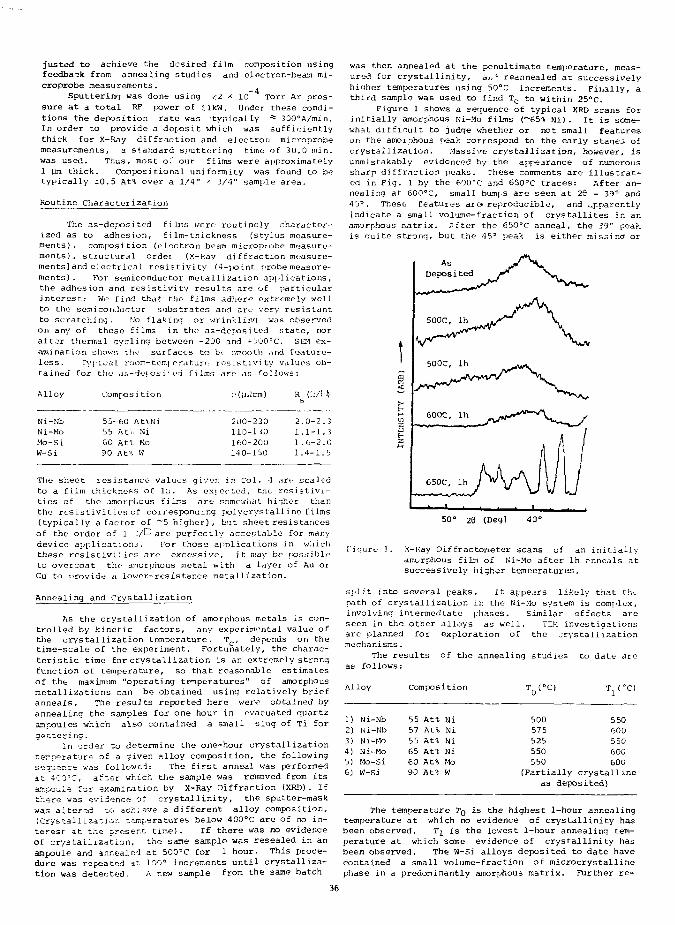
justed to achieve the desired film composition usingfeedback from annealing studies and electron-beam mi-croprobe measurements.
Sputtering was done using ^2 * 10*" Torr Ar pres-sure at a total RF power of <lkW. Under these condi-tions the deposition rate was typically * 300°A/min.In order to provide a deposit which was sufficientlythick for X-Ray diffraction and electron microprobemeasurements, a standard sputtering time of 30.0 man.was used. Thus, most o~ our films were approximately1 urn thick. Compositional uni formity was found to betypically 10.5 At% over a 1/4" * 3/4" sample area.
Routine Characterization
The as-deposi ted films were routinely character-ized as to adhesion, film-thickness (stylus measure-ments), composition {electron beam micropiobe measure-ments) , structural order (X-Ray diffraction measure-ments) and electrical resistivity (4-point probe measure-ments) . For semiconductor metallization applications,the adhesion and resistivity results are of particularinterest: We find that the films adhere extremely wellto the semiconJuctor substrates and are very resistantto scratchi ng. No flaking or wrinkliivi was observedon any of these films in the as-depositod state, noraf t r thermal cycli ng between -200 and +500DC. SEM ex-amination shov/K the surfaces to be- smooth and feature-less. Typical room-temperaturo res istivi ty values ob-tained for thu as-doposi'ed f ilms are as follows:
Alloy Compos i tion
Ni-NbNi-MoMo-SiW-Si
55-6055 At.60 At!90 SO
AttNi. Ni, Mo
W
200-230110-130160-200140-150
2111
.0-2
.1-1
.6-2.4-1
. 3
. 3
. 0. 5
The sheet resistance values given in Col. 4 art- scaledto a f ilm thickness of lii. As extorted, the resistivi-ties of the amorphous films are somewhat higher thanthe resistivities of coiresponding polycrystalline films(typically a factor of 5 higher) , but sheet resistancesof the order of 1 ":/O are perfectly acceptable for manydevice applicat ions . For those applications in w!ii chthese resistivities are excessive, it nay bo possible1
to overcoat the amorphous metal with a layer of Au orCu to provide a lower-resistance metallization.
Annealing and Crystallization
As the crystallization of amorphous metals is con-trolled by kinetic factors, any experimental value ofthe crystallization temperature, Tc, depends on thetime-scale of the experiment. Fortunately, the charac-teristic time for crystallization is an extremely strongfunction of temperature/ so that reasonable estimatesof the maximum "operating temperatures" of amorphousmetallizations can be obtained using relatively briefanneals. The results reported here were obtained byannealing the samples for one hour in evacuated quartzamijoules which also contained a small slug of Ti forgettering.
In order to determine the one-hour crystallizationtsr.cerature of a given alloy composition, the followings-sauerice was followed: The first anneal was performedat 400'Z, after which the sample was removed from itsampoule for examination by X-Ray Diffraction (XRD). Ifthere was evidence of crystallinity, the sputter-maskwas altered to achieve a different alloy composition.{Crystallization temperatures below 400°C are of no in-terest at the present time). If there was no evidenceof crystallization, the same sample was resealed in anampoule and annealed at 500°C for 1 hour- This proce-dure was repeated at 100° increments until crystalliza-tion was detected. A new sample from the same batch
was then annealed at the penultimate temperature, meas-ured for crystallinity, a,.4 reannealed at successivelyhiqher temperatures using 50°C increments. Finally, athird sample was used to find Tc to within 25°c.
Figure 1 shows a sequence of typical XRD scans forinitially amorphous Ni-Mo films (""65% Ni) . It is some-what difficult to judge whether or not small featureson the amorphous peak correspond to the early stages ofcrystallization. Massive crystallization, however, isunmistakably evidenced by the appearance of numeroussh^rp diffraction peaks. These comments are illustrat-ed in Fig. 1 by the 600°C and 650°C traces: After an-nealing at 600°C, small biun s are seen at 26 = 39° and45°. These features arc* reproducible, and apparentlyindicate a small volume-fraction of crystallites in anamorphous matrix. Pfter the 650°C anneal, the 39° peak-is quite strong, but the 45° peak is either missinq or
50° 26 (Deg)
Fiqure 1. X-Ray Diffractoraeter scans of an initiallyamorphous film of Ni-Mo after In rnncals atsuccessively higher temperatures.
split into several peaks. It appears likely that tht.path of crystallization in the Ni-Mo system is complex,involving intermediate phases. Similar effects areseen in the other alloys as well, TEM investigationsare planned for exploration of the jrystallizationmechanisms.
The results of the annealing studies to date areas follows:
Alloy Composition
1)2)3)
4)5)
6)
Ni-NbNi-NbNi-MoNi-MoMo-SiW-Si
555755656090
At%At".At%At%At%At%
N iNiNiNiMoW
500575525550550
550600550600600
(Partially crystallineas deposited)
The temperature TQ is the highest 1-hour annealingtemperature at which no evidence of crystallinity hasbeen observed. T^ is the lowest 1-hour annealing tem-perature at which some evidence of crystallinity hasbeen observed. The W-Si alloys deposited to date havecontained a small volume-fraction of microcrystallinephase in a predominantly amorphous matrix. Further re-
36
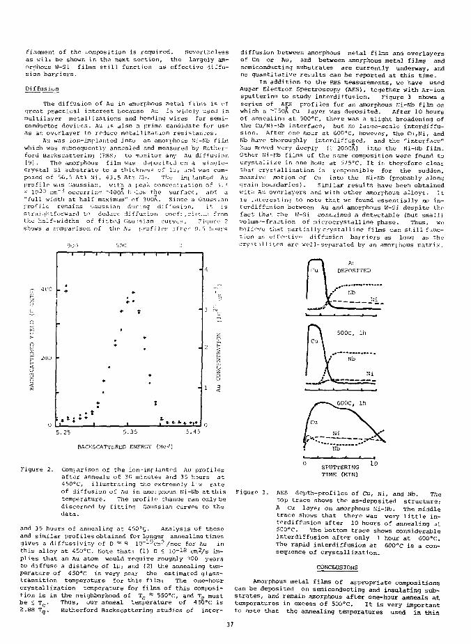
finement of the composition is required. Neverthelessas wilj. be shown in the next section, the largely am-orphous W-Si films still function as effective diffu-sion barriers.
Diffusion
The diffusion of Au in amorphous metal films is ofgreat practical interest because Au is widely used inmultilayer metallizations and bondinu wires for semi-conductor devices. Au is also a prime candidate for useas an overlayer to reduce metallization resistances.
Au was ion-implanted into an amorphous H:'-Nb filmwhich was subsequently annealed and measured by Ruther-ford Backscattering (PBSt to monitor any Au diffusion[9]. The amorphous film was dejx>sitcd on a single-crystal Si substrate to a thickness of IJJ , and was com-posed of 56.5 At% >ii , 43.5 .At?. Kb. The in[lanted Auprofile was Gaussian, with a peak concentration of 3.^x io2O cm""3 occurring ~400A I- 'low the surface, and a"full width at half maximum" of 300A. Since a Gaussianprofile remains Gaussian during diffusion, it isstraightforward to deduce diffusion coefl . ri <•:.,„; fromthe half-widths of fitted Gau-.sian curve:?. Figure 2shows a comparison of the hu profiles ,-;fter 0.0 hours
400 -
5
5.25 5.35 5.45
BACKSCATTERED ENERGV (MeV)
Figure 2. Comparison of the ion-implanted Au profilesafter anneals of 30 minutes and 3 5 hDurs at45O°C, illustrating the extremely 1 w rateof diffusion of Au in amoi pnaus Ni-Nb at thistemperature. The profile change can only bediscerned by fitting Gaussian curves to thedata.
and 35 hours of annealing at 450°g. Analysis of theseand similar prof iles obtained for longer annealina timesgives a dlffussivity of D * 8 10"^5cm2/sec for Au inthis alloy at 450°C. Note that: (1) D < 10-18 cm2/s im-plies that an Au atom would require roughly 300 yearsto diffuse a distance of 1M; and (2) the annealing tem-perature of 450°C is very near the estimated glass-transition temperature for this firm: The one-hourcrystallization temperature for films of this comjxDsi-tion is in the neighborhood of Tc * 550°c, and Tg mustbe < Tc- Thus, our anneal temperature of 450°c isS.88 Tg. Rutherford Backscattering studies of inter-
diffusion between amorphous metal films and overlayersof Cu or Au, ana between amorphous metal films andsemiconducting substrates are currently underway, andno quantitative results can be reported at this time.
In addition to tile RBS measurements, we have usedAuger Electron Spectroscopy (AES), together with Ar-ionsputterinn to study interdiffusion. Figure 3 shows aseries of AES profiles for an amorphous !Ii-Kb film or.which a ~75OA Cu layer was deposited. After 10 hoursof annealing at 500°C, there was a slight broadening ofthe Cu/Nj-!Jb interface, but no large-scale interdiffu-sion. After one hour at 600°c, however, the Cu,Ni, andKb have thoroughly interdiffused, and the "interface"has moved very deeply (I 2000A) ir.to the Ni-Ub film.Other Ni-r:b films of the same composition were found tocrystallize in one hour at 575°C. It i:. therefore clearthat crystallization is responsible for the sudden,massive motion of Cu into the Mi-rib (probably alonggrain boundaries). Similar results have been obtainedwitii Au overlayers and with other amorphous alloys. Itis interesting to note that we found essentially no in-terdiffusion between Au and amorphous W-Si despite thefact that the W-Si contained a detectable (but small)volume-fraction of microcrystalline phase. Thus, webelieve tiiat partially crystalline films can still func-tion as ei'fertiv" diffusion barriers as long as thecrystallites are we]1-separated by an amorphous matrix.
A:DEPOSITED
500C, lh
600C, lh
SPUTTERINGTIME (MIN)
10
Figure 3. AES depth-profiles of Cu, Ni, and Nb. Thetop trace shows the as-deposited structure:A Cu layer on amorphous Ni-Nb. The middletrace shows that there was very little in-terdiffusion after 10 hours of annealing JL500°C. The bottom trace shows considerableinterdiffusion after only 1 hour at 600°C.The rapid interdiffusion at 600°C is a con-sequence of crystallization.
CONCLUSIONS
Amorphous metal films of appropriate compositionscan be deposited on semiconducting and insulating sub~strates, and remain amorphous after one-hour anneals attemperatures in excess of 500°C. It is very importantto note that the annealing temperatures used in this
37
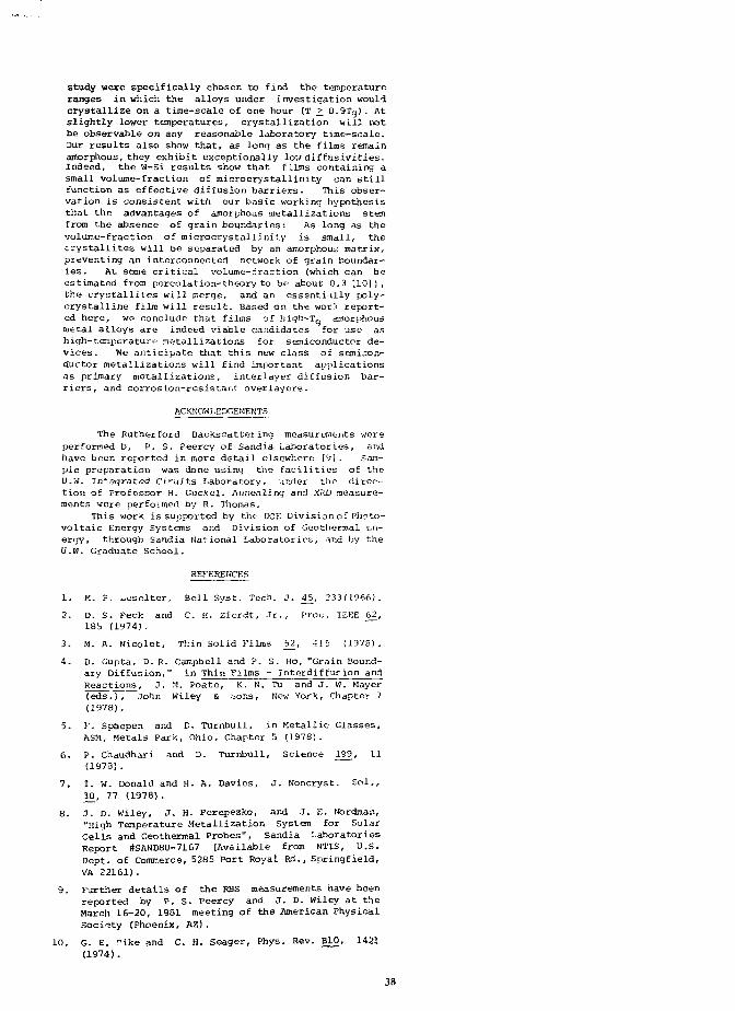
study were specifically chosen to find the temperatureranges in which the alloys under investigation wouldcrystallize on a time-scale of one hour (T >_ 0.9Tg) . Atslightly lower temperatures, crystallization will notbe observable on any reasonable laboratory time-scale.Our results also show that, as long as the films remainamorphous, they exhibit exceptionally low diffusivities.Indeed, the W-Si results show that films containing asmall volume-fraction of microcrystallinity can stillfunction as effective diffusion barriers. This obser-vation is consistent with our basic working hypothesisthat the advantages of amorphous metallizations stemfrom the absence of grain boundaries: As long as thevolume-fraction of microcrystalliriity is small, thecrystallites will be separated by an amorphous matrix,preventing an interconnected network of grain boundar-ies. At some critical volume-fraction (which can beestimated from percolation-theory to be about 0.3 [101),the crystallites will merge, and an essentially poly-crystalline film will result. Based on the wor!'. report-ed here, we conclude that films of high-Tg amorphousmetal alloys are indeed viable candidates for use ashigh-temperature metallizations for semiconductor de-vices. We anticipate that this new class of semicon-ductor metallizations will find important applicationsas primary metallizations, interlayer diffusion bar-riers, and corros ion-resistar.t- overlayers.
ACKNOWLEDGEMENTS
The Rutherford Backscattering measurements wereperformed b, P. S. Peercy of Sandia Laboratories, andhave been reported in more detail elsewhere [y]. Sam-ple preparation was done using the facilities of theU.w. Integrated Ci^uits Laboratory, under the direc-tion of Professor H. Guckel. Annealing and XRD measure-ments were performed by R. Thomas.
This work is supported by the DOE Division of Photo-voltaic Energy Systems and Division of Geothermal En-ergy, through Sandia National Laboratories, and by theU.W. Graduate School.
REFERENCES
1. M. P. ^oselter, Bell Syst. Tech. J. 4j>, 233(1966).
2. D. S. Peck and C. H. Zierdt, Jr., Proc. IEEE 6£,185 (1974).
3. M. A. Nicolet, Thin Solid Films S2_, 415 (1978).
4. D. Gupta, D. R. Campbell and P. S. Ho, "Grain Bound-ary Diffusion," in Thin Films - Jnterdiffurion andReactions, J. M. Poate, K. N. Tu and J. W. Mayer(eds.), John Wiley & bons. New York, Chapter 7(1978).
5. F. Spaepen and D. Turnbull, in Metallic Glasses,ASM, Metals Park, Ohio, Chapter 5 (1978).
6. P. Chaudhari and D. Turnbull, Science 199, 11(1979).
7. 1. W. Donald and H. A. Davies, J. Noncryst. Sol,,30, 77 (1978).
8. J. D. Wiley, J. H. Perepezko, and J. E. Nordman,"High Temperature Metallization system for SolarCells and Geothermal Probes", Sandia LaboratoriesReport #SAND80-7167 (Available from NTIS, U.S.Dept. of Commerce, 5285 Port Royal Rd., Springfield,VA 22161).
9. Further details of the RBS measurements have beenreported by P. S. Peercy and J. D. Wiley at theMarch 16-20, 1981 meeting of the American PhysicalSociety (Phoenix, AZ).
10. G. E. Pike and C. H. Seager, Phys. Rev. BIO, 1421(1974).
38
OHHIC CONTACTS TO GaAs FOR HIGH-TEMPERATURE DEVICE APPLICATIONS
W. T. Anderson, Jr., A. Christou, J. F. Giuliani and H. B. DietrichNaval Research LaboratoryWashington, D. C. 20375
Ohmic contacts to n-type GaAs have been developedfor high-temperature device applications up to 300°C.Refractory metallizations were used with epitaxial Gelayers to form the contacts: TiW/Ge/GaAs, Ta/Ge/GaAs,Mo/Ge/GaAs, and Ni/Ge/GaAs. Contacts with high doseSi or Se ion implantation (1012 to 1014/cm2) of theGe/GaAs interface were also investigated. The purposeof this work was to develop refractory ohmic contactswith low specific contact resistance (~10 fi-cm2 onlxlO17/cm3 GaAs) which a^e free of imperfections,resulting in a uniform N doping layer.
The contacts were fabricated on epitaxial GaAslayers (n=2x]016 to 2xlO17/cm3) grown on N (2x20l8/cm3)or semi-insulating GaAs substrates. Ohmic contact wasformed by both thermal aii^paling (at temperatures upto 700°C) and laser annealing (pulsed Ruby). Examina-tion of the Ge/GaAs interface revealed Ge migrationinto GaAs to form an N doping layer.
Under optimum laser anneal conditions, the spe-cific contact resistance was in the range 1-5x10 fl-cm2
(on 2xlO17/cm3 GaAs). This is an order of magnitudeimprovement over thermally annealed Ag/Si1 or Ni/Ge2
contacts. Thermally,annealed TiW/Ge had a contactresistivity of 1x10 Qcm2 on lxlO17/cm3 GaAs underoptimum anneal conditions. The contacts also showedimproved thermal stability over conventional Ni/AuGecontacts at temperatures above 300°C. The contactresistivity of thermally annealed TiW/Ge does notincrease appreciably with a 350°C, 190 hr anneal, whilethat of Ni/AuGe degrades appreciably between 25-35 hrsat 350°C. Under bias conditions (6V, 15 mA) the con-tact resistance of these contacts did not increaseappreciably at 300°C after 160 hr. Preliminary resultswith the laser annealed contacts showed no measurableincrease in resistance after 6 hr at 350°C.
Introduction
Low specific contact resistance ohmic contacts ton-type GaAs using epitaxial Ge films have been reportedusing molecular beam epitaxy3 and vacuum epitaxy.2'4
The epitaxial Ge film allows (in theory) the formationof contacts with a uniform N layer, in the highlydoped Ge film itself3 or, from Ge doping of the GaAs.2'4
These contacts should be more nearly free of imperfec-tions compared to polycrystalline Ge or AuGe entecticfilms in which rapid impurity diffusion occurs at grainboundaries. Both thermal annealing and laser annealinghave been used to form ohmic contact. Laser annealingwas used to form these contacts5 because when a refrac-tory metal overlayer is desired it was found2'4 thatoven anneal temperatures in the range 500-750°C wererequired. Subjecting the entire substrate to thesehigh temperatures can have deleterious effects on theactive and semi-insulating GaAs layers and to othermetallizations previously deposited on the chip, e.g.,for the purpose of fabricating integrated circuits.This problem can be obviated by selective contactannealing with a laser beam. Pulsed laser annealingmay also be important in obtaining enhanced activationof implanted dopants and in obtaining certain dopingprofiles when rapid heating and cooling are important.
In this paper we report on TiW (88 wt. % W, 12wt. % Ti)/Ge, Ta/Ge, Mo/Ge, and Ni/Ge ohmic contactsto n-type GaAs which have two possible areas of appli-cations: 1) to devices which are designed to operatefor extended periods of time in a high temperature
ambient (above 150°C)1, and 2) to improve the reliabil-ity of devices which experience high channel or contacttemperatures, such as pover field-effect transistors(FET) and transferred-electron devices (TED).6 In bothcases, local melting at imperfections in the contactscan result in device failure. Formation of an N layerat the GaAs-contact interface by Ge doping can alsoresult in significant performance gains in power FETsand TEDs through reduction in contact resistance andincreased voltage levels.
Experimental Method and Results
Fabrication of the ohmic contacts was similar tothat described previously.2 A number of differenttypes of contacts were investigated: TiW/Ge, Ta/Ge,Mo/Ge, and Ni/Ge, both wjt'a and without a high dose ofSi or Se ion implanted (I2) at the Ge/GaAs interface.Ohmic contacts were fabricated on n-type epitaxial GaAslayers with carrier a concentration of 2xlOI7/cm3 grownon N (100) oriented GaAs substrates doped to 2xlO18/cm3
or on GaAs epitaxial layers (n=lxl017/cm3, 20008 thick)grown on semi-insulating (SI) GaAs substrates. To pre-pare the GaAs surface for growth of the epit xial Gelayer, the surface was cleaned in organic solvents,etched in a solution (10 mi HC£, 10 mi HF, 40 m£ H,0,6 drops of H_0_) to remove carbon and oxyge.i, and ~placed immediately into a high vacuum system. Oxideswere desorbed by heating_the substrate to 575°C for 15min in a vacuum of 2x10 Torr. Oxide desorption wascarried out at 575°C because it was found4 by Augerelectron spectroscopy (AES) that the oxide concentra-tion was at a minimum at this temperature withoutgreatly changing the GaAs stoichiometry. An epitaxialGe layer was then grown in the same vacuum at 425°C tothicknesses between 200 to 2000A by electron beam evap-oration from pure Ge source. For contacts on N sub-strates, circular Ge contact patterns (30 to 250 um indiameter) were formed by etching 3nd the metal over-layers were deposited to thicknesses between 1000 to20008 (by electron beam evaporation in the case of Ta,Mo, and Ni; and by sputtering in the case of TiW).Isolated circular contact patterns were defined usingphotoresist and lifting or by performing the Repositionthrough a metal mask. Ohmic contact to the N backsidewas made with AuGe/Ni, alloyed at 450°C far 15 secprior to fabrication of the frontside contacts. Typicalcontacts are shown in Fig. 1. In the case of TiW/Ge/I2
Si contacts to the GaAs epitaxial layer on SI sub-strates, transmission line model (TLM) contacts wereformed by etching the mesa, TiW, and Ge in three sep-arate etching steps.
100t
1
t
650 A TiWA [~^ 1200 A Epi Ge j
I2 N* LAYERN = 2 x 1016 cm"3 GaAs Epi
N+ = 2 x 1018 cm"3 GaAs
\ AuGe/Ni(IMPLANTED Si
- 175 keV, Sx 10" cm"2
(200 keV. 3 x 10" cm"2
0.52^m
11000 A Ni
1000 A Epi Ge
N = 2 x 10" cm"3 GaAs
N* GaAs
AuGe/Ni /
oTi5f.ni
Fig. 1. Schematic cross sections of typical refractorymetal/Ge ohmic contacts to GaAs.
39
Thermal annealing of the TiW/Gc 'lAbi contact:(1500S TiW/40oS Gen-Si at 60kcV, 2xIU1Vcm') was car-ried out in forming gas al 700°C. Near optimum anneal-ing conditions,of 25 nun, the specific contact resist-ance was 1x10 Dcra2 as measured by the Tl.M method.8
Au^er electron spectroscopy (AF.S) sputter profiles, asdeposited and after sintering in vacu^it, arc shown inFig. 2. After sintering, Ge migration into GaAs wasobserved indicating an N doping layer at the GaAssurface. This condition is necessary tot a low spe-cific cuiitact resistance.s The Si implant may alsohave been partially activated resulting in a furtherincrease in the concentration of the N doping layer.After 2S miu at ?00°C, Ga outdiffusion was alsoobserved, allowing vacant sites fo: G<? or Si doping
SPUTTER TIME. M1N
100,
2S 50 75SPUTTER TIME M I N
(b)
Fig. 2. AES sputter profile of TiW/Ge/Ga.As contact,la) as deposited and (b) after ohmic contact tormaliiinat 700°C for 15 min at JO 7orr.
Laser annealing was perfoTned with a ruby laserwhich emitted a one joule, 22 us pi;ise obtained by•^-switching the cavity with a Pockel's cell. Experi-ments rfere performed both in single TEH., mode and inmuitiroode operation. The single mod° was used for thesmall diameter ohnuc contact experiments while themultimode was employed for large area AES analyses.For tl/e TEM00 mode rase, a 0.8 mo circulzr aperturewas placed in the optic 1 cavity. The output beam wasthen focused to fornj a 260 um diameter spot al thesample. A 30 to 50 um diameter cpot, which containedonly the center of the Gaussian beam, was obtained byuse of a metal mask. Ohmic contacts were obtained atenergy densities between 0.09 to 5 J/cm , depending onthe type of contact. For the multioiode case, the fullone joule output was Iiomogenizod by a method similarto that described by Cullis, el al.7 by sending itthrough a 1.2 cm diameter fused quartz optical waveguide whi h was bent and tapered to obtain a spot
diameter at the sample rf 0.7 cm. Although this "lightguide diffuser" was effective in. homogenization of themulumode structure of the beam and reducing specklepatterns, "hot spots" vere still observd at the output(particularly apparent on CiAs surfaces). A detailedanalysis of the appearance of hot P^ots will be pub-lished later.
Cutrent/volta,;e (1/V) characteristics of a typicalNj/Ge contact before and after laser annealing aresi own ii> Fig. 3 as displayed on a curve tracer. Beforelaser annealing the contacts were reasonably wellhchaved Schottky barriers; the upper curve shows areverse breakdown voltage of about 5 volts on 2xlOI7/cm^doped GaAs. Afier a pulse of 0.04 J/cmz the rectifica-tion softens, indicating some very limited melting,perhaps associated with preferentially absorbing imper-fections 0,1 the top surface. At 0.!6 J/cm2 the contactwas ohmic an»! the phc-toratcrograph of this contact,siiuwn 111 fig. 3. indicated very shallow, uniform melt-ing had occurred. Similar results were found withTiW/Ge, Mo/Ge, and Ta/G» contacts.
BEFORE LASER ANNEALVERT: S00/(A/divHOR: 1 V'div
0.04 J'cm2. 1 pulseVERT: 500 /;A/divHOB. 100rnV !iv
O.t4VERT: 20 mA.div PHOTOMICROGRAPH.HOR: lOOmVfdiv/ O.TJJ/cm*
tig. 3. Curve tracer 1/V curves of Ni/Ge/GaAs contactsbefore laser annealing and after Laser annealing at0.04 J/cm2 (soft Schottky barrier) and 0.14 J/cm2 (suf-ficient energy density to form ohroic contact). Photo-micrograph of online contact after 0.14 J/cro'.
Experimental curves of the specific contactresistance versus laser energy density are shown inFig. 1. Measurements were made with a method siailarto that of Cox and Strack.10 These results wereobtained using the TEMQ 0 mode with a 30 to 50 \indiameter metal mask over (typically) 250 \m diameterj&olated contacts. Approximate welting points for eachof the contact types are shown at the top, as deter-mined from photomicrographs of the irradiated surfaces.However, the melting points could not be determinedprecisely from the photomicrographs and very shallowmelting probably occurred below these points. It wasfound that tho •ontact resistivity was at a niniauonear tbe melting point for Ni/Ge and Ta/Ge contacts.Similar Til./Ge ohmic contacts 10rued on n=2x!0l6/c«3
GaAs epitaxial layers resulted in a specific contactresistance of 1x10 flcms. The higher value of spe-cific contact resistance evidently resulted froa thelowti doping in -be GaAs. Similarly, contact resistiv-ity values for Ta/Ge, Mo/Ge, and Ni/Gf? were approxi-mately an order of magnitude higher on 2xI016/cra3 ascompared to 2xlO17/cm5 GaAs.
10 3
i Gf mi> T* Ge mp
Mo Gt
t 1 !
1000 \Ta 1000 \Ctr
<LSI
CO
Ni
• ' Mi
G- Ga
Gr Ga
a G*> G
At,
IAS
§io'-o
P"ISED ftuBV CAStfl
. Mr, 1000 '. Gr
ENERGY DENSITY IJ cm'
Fig. 4. Experimental \ allies <>f specific contact resist-ance 35 a function pulsed ruby laser energy density;mp indicates approximate melting points is determinedfrom surface photomicrographs.
The interfaces before and after laser ar.ru*.»1 ing
Kfif investigated using AF.S sputter profiling tech-
niques. Figure 5 shows AtS sputter profiles of a Si/Or
contact hefore laser annealing and after laser anneal-
ing at an energy density just high enough to form ohfinc
contact. A raultimode 7 mm diameter beam was used to
irradiate a GaAs sample approximately 10 mm x 10 .Tun
containing 2000S Ni and 2000.$ Ge prepared as discussed
above. At 0.10 J/cm- slight melting patterns could
just be observed, indiciting u< Itn.g of the Si and Ge
just to, and including, the GaAs surface. Tl;is energv
density corresponded to the threshold for ohmic contact
formation. Even at this low energy density there was
G" migration into the GaAs, enough to greatly imicije
the n-type doping concentration at thr GaAs surlace.
Similar profiles were observed with Ta/Ge laser
annealed contacts. These profiles are also typical >f
Ni/Ge thermal annealed ohmic contacts studied pre-
viously.2
SPUTTER TIME (mini
Fig. 5. AES sputter profiles of a 2OOo8 Ni/2QOu8
Ge/GaAs contact before laser annealing and after laser
annealing at 0.10 J/cm2, just at threshold for ohmic
contact formation.
Discussion of laser Anneal Results
The curves of specific c o m iCt resistance versus
energy density, shown in Fig. 4, indicate there is a
"window" in energy density which is appropriate for
the formation oi ohmic contact. This window depends
*.n the layer thicknesses of tne metal and epitaxial
0 , the pulse duration, to some extent on the surface
morphology, Jitd also n the fundamental interaction^11
of the laser lii-am with the overlayrrs and O.iAs. The
di-|.:h of melting and surface te»perature are deter-
mined in ^ art by the absorption coefficient, specific
heat, and thermal diffu.sivity of the overlayt'rs and
GaAs surfaic. uhnuc contact appeared to occur just at
the threshold of nelting, but the me'ting rousl b*' deep
enough to melt .it least the top 50 to 100S of the GaAs
surface lo account for the AES profiles m rig. 5.
Solid-stlte diffusion proci- ;ses art tori slow lo .ltrouil
for these prof..<'s. Since the heating and cooling
rates j-r nearly the same in pulse laser annealing
dominated by thermal processes,11 the Ge migration into
the GaAs surface must ovcur in the 50-300 ns thai Ihr
surf '.i' layers are rr.oiten. A minimum ir. the specifir
cfnt Mt rrsist<incc> apparently occurs just above 1m-
melting JJOI it at an op Li mum doping U'vel and pi.ifi'e
It ..s assumed tuat low contact resistance occurs by
elei irons tiir.n.-! IIIR bc-tveen the top metal layer and
the highly doped surface iayer in the GaAs. 3 The spo-
c ific contact resistance begins \n rise at higher
energy densities as tlu1 melt penrtration becomes deeper
.iivi the surtjirr tcnijici^ture reaches the boiling point.
Surface evaporat ion ,iml oblation i .in then result m
loss of Gt' and As (as well as loss of part of the [petal
contact), as has been observed with these contacts al
high energy densities by electron microprobe x-ray
analysis. This was found to result m an increase in
the specific contact resistance-
The advantages c laser annual in? over thermal
annealing for these ^articular high-te-niijcrature con-
tacts is seen in comparison with I hernia! annealing
results. For similar ohnu contacts, tin- specific con-
ta t resistance was more than an order of magnitude
higher wiien thermallv annealed*" an<l b i gh irnhienT tern"
peratures (u]> tu f?5o°C for 5 mini w r re«iuired. the
laser annealed contacts rcnorted heie also demonstrate
jn or.Jer oi magnitude improvement in contact resistiv-
ity over Ag/Si tont.ic's1 thfrmally annealed. These
ronl K t s .'I!S<J t > nare (avoraj)ly with conventional AuGe
nhmn coguits. for winch a specific contact resistance
o( !x 10 '..'tm" ran be routinely obtained, but which
degrade s ; gi<j f J t ant 1 y at 35O°C.
H^h-Temperatiire Aging
The TiW/Ge/I2S: olimic contacts formed on GaAs epi-
taxial layers un SI substrates and theraaily annealed
were studied by high lempeature aging in an ambient of
forming gas. Figure 6 shows the change in the specific
contact resistance uftrr exposure to tercperatures
between 350 to 600°C for over 175 hours. The behavior
of a typical AuGe/N'i contact, included in the 3 5 C C
experiments, is shown for comparison. Thrse results
demonstrate the high-temperature reliability advantages
of refractory metal/epitaxial Ge ohmic contacts. With
these contacts it was found that the contact resistance
did not increase appreciably up to 190 hours at 350°C,
whiLe that of AuGe significantly increased between
25-35 hours at 35O°C.
Preliminary high-temperature aging experiments
with the laser annealed ohmic contacts (TiW/Ge/I2Si,
Ni/Ge/I2Si, Ni/Ge, Ta/Ge, aiid^Mo/Ce) were also carried
out by aging in vacuum at 10 Tore. So measurable
change in specific contact resistance was found after
350°C for 6 hr.
The thermally annealed TiW/Ge ohoic contacts were
also subjected lo high-temperature aging under DC bias.
41
Figure 7 shows the results; at 3OQ°C and 35O°C after
exposure for 160 hr At 300°C the contact resistivity
increased initially out stabilized at about wx!0~ Qcm2.
At 35J°C the increase in contact resistivity was much
larger. This was partially explained by the large out-
diffusion of C J , shown in the ASS sputter profiles in
Fig- 8.
1-10 '
o115050 75 )00 1JS
ANNEAL DURATION HOURS
Fig. b. Spi -nf ic l o n U i l r e s i s t a n o of t.'.ermallyannealed TiW/Ge anil AnCe/Si ohsui* contac ts j i a <un<-l ion of annea 1 t i*ne .it various aging teraperattirt'.s informing ga.%.
O 0 20 40 60 «O 100 130 1*0u ANNE At TIME. HOURS
Fig. 7. Specific contact resistance of thermallyannealed TiW/Gr contacts as a function of inneal limeunder bias conditions at 300"C and VJ»°C m forminggas. Test structure used to measure contact resistiv-ity (center mesa) and to study metal migration (longarms).
S I R . fc. Af.S s p t i t e r p r o f i l e (Gc and Ga) of t h t r a a i l yaniie.iled TiW/oe ohmr itmiacl a f t e r 350°C/ii0 hr annealin lorninK «.»s up.der iuqs coutlil :o;is, i>hc.wi:.g large Ga"ui.lif fusion
Acka^w 1 ed£c~erit s
Tht- ,! Jth^rs wish to th3n&: Dr. J E. Davey. Head oftiic Solid State Devices Branch, and ! . . I..F. Druflweter.toracr .iuperinlen<ltnt ot the Optical Sciences Divis ion,for active- support of t h t s work- The authors a l so wishto acknowledge the a s s i s t ance of B. Wilkins i:i A£Ssieasurereents .ind .1. Bark m sample process ing.
Heferences
1 J.A. Coquat. D.W. Palner, O. Eknoyan. and W.B.Van der Uneven. I960 Proceedings Electronic Com-ponents Conl. (1EKE. Sew York, 1980), pp. 55-60.
2. W.T Anderson, Jr., A. Chnstou, and J.E. Davey,IEEE 1. c.f Solid-State Circuits, Vol. SC-13, So. i.pp. ii0-4i5, Aug. I97S.
}. K Stall, C.E.C. Wood, K. Board anil L.F. Eastman.Electronic Lett., Vol. 15, pp. 800-SOi, Z2 Nov] 17<>.
^. A. Christou, J.E. Davey, H.B. Dietrich, and W.T.Anderson, Jr., i7th Anni-j Device Research Conf.,University of Coiorado, Boulder, Colorado. June25-27, 1979.
5. W.T. Anderson, Jr., A. Chiislou, H.B. Dirtrich,and J.F. Giuliani, 158th Meeting of the Electro-ch.-micaJ Society, Hollyvood, Florida, Oct. 5-10,1980.
6. W.T. Anderson, Jr., and A. Chnslou. 1980 Workshopon Compound SeBiconductors for Microwave Materialsand Devices, San Francisco, H-12 February 1980.
7. A.G. Cullis, H-C. Webber, and P. Bailey, J. Phys.E: Sri. lustrum.. Vol. 12, pp. 688-689, 1979.
f H.H Berger. J. Electrochea. Soc, Vol. 119, p.507. J9/2.
9. C.Y. Chang, V.K. Fang, and S.M. Sxe, Solid-StateElectronics. Vol. 14, pp. 5-1-550, 1971.
10. R.H. Cox and H. Strack, Solid-Statt Electronics.Vol. 10, pp. 1213-1218, 1967.
11. N. B)oe»bergen, in Laser-Solid Interactions andLaser Processing-1978, S.D. Ferris, H.J. Le»yand J.H. Poale, Ed., Sew York: American Instituteof Physics, 1979, pp. 1-9.
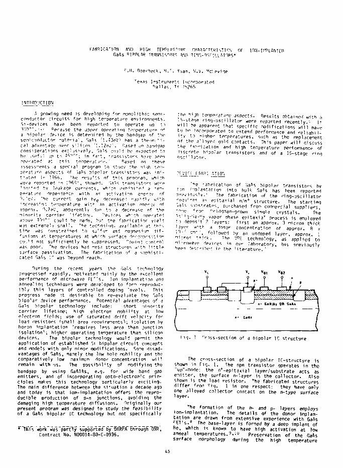
FABRICATION AND HIGH TF.Mr'r_PSTMSjrGaAs ^POLAft TqA>)S!STns>S Vm
OF 10N-IHPLANTEI1
r . H . DoerhecV., ' I . * . Yuan, W.V. Vcl.eviqe
Texas Instruments IncorporatedDa l l as , TY
INTonp'JCTlON
'. growing need is developing for monol i thic seni-cond'jctor c i r c u i t s for high temperature environnents.Si-devices ha/e been reported to operate up ; i700°" . *»• Rprause the upper operatinq tenperaturp o*a b ipo lar device is determined hy the bandgan of thpsemiconductor mater ia 1 , ' ia 's ' ! .43eVl has a t h e o r i ' i -cal advantage over s i l i c o n " . . ' . ?p;M . Hasei on haod'japconsiderat ions excl JS*ve l y . 'ia-ls could be expected tobe i s e f j ! jp to 4 S T " ; in f a r t , t rans is to rs neve beenoperated at t h i s tenpera t ; rp . • ^ased on theseassessments a special program to study the hiqh tpm-oera t j re aspects of iaAs b ipolar t rans is to rs was i n i -t 'ate<i in ' .%6 . The resu ' t s of t h i s prooran, whi:hwere reported in ' .^R"1 , showed: ".a"s t rans is to rs were' i n s e r t hy leaS-aqe cur rents , whi-h e^hibi-p.) $ *en-pprat j re dependence wi th an ac t i va t ion ene*"r;v of1."e-.'. rhe current gain hfe decrease' r a p i d ' • w' th'ncreas'nq temperature with an ac t i va t i on .->np'-;v ofaoprox. i . ?pv , apparently due to a decease of the- l i no r i t y ca r r i e r M f e t i i ' e . '^evices w h ' t h opp'-atedabove W l ° ~ o u l d he nade, but the fabr i ca t ion y ie ldwas ex t re-e ly s n a l ! . The techno'oq-, ava i i ab l " at *h:st i ne was constrained to su l fu r and nagnes'un l i f -'us ions at tenpc"atures at which surface dpr^npos1tiorCO'.1"! not s u f f i c i e n t l y he suppressed. Ion in"; c o n f o lwas poor. *he devices had -.esa structures w' th l i t t l esurface pass iva t ion . The fab r i ca t ion of a soph is t i -cated ria>'.s '.' was beyond reach.
l u r i n g the recent years the "ia-'s technologyprogressed r a p i d l y , not ivated nainly by the excel lentperfornance of microwave FET's. Ion inp lan ta t ion andannealing techniaues were developed to forn reproduc-i b l y t h i n layers of cont ro l led doping leve ls . Thisprogress made i t desirable to re-evaluate the 'iaRsb ipo la r device performance. Potent ia l advantages of aSa's b ipolar technology include: short minor i tyc a r r i e r l i f e t i n e ; high e lect ron n o b i l i t y at lowe lec t ron f i e l d s ; use of saturated d r i f t ve loc i t y forload res is to rs ' sna i l area requirenents^; i ; o l a t i o n byboron inplantation (requires less area than junctionisolat ion1 ; higher operating temperature than si l icondevices. The bipolar technology would pemit theapplication of established Si bipolar c i rcui t conceptsand models with only ninor modifications. Some disad-vantages of GaAs, nanely the low hole mobility and thecor.paratively low naximun donor concentration wi l lrenain with us. The possibi l i ty of noriifyinq thebandgap by using GaAlAs, e.g. for wide band gapemitters, and of incorporating ODto-electronic prin-ciples makes this technology oarticularly excit ing.The nain difference between the situation a decade agoand today is that ion-implantation offers the repro-ducible production of p-n junctions, avoiding thedamaging high temperature diffusions. Originally ourpresent program was designed to study the feas ib i l i t yof a GaAs bipolar IC technology but not specif ically
* This"work was partly supported"by OARFA through OflFf,Contract No. N00014-80-C-0936.
the h i jh tenperat'ire asnects. Results obtained with a.->-sta<ie r ing-osc i l la tor were reported recently - I tw i l l be apparent that specif ic nodif ications w i l l na.eto be incorporated to extend performance and r e l i a b i l -i t y to higher temperatures, such as the replacementof the alloyed qold contacts. This paper w i l l discussthe fah-icat ion and high temperature performance of•1 iscrete bipolar transistors and of a I5-staqe rinoosc i l l a to r .
HjVJr ! ATlQ'i
prev•/eq.id's^nne• • " > ' !
to d1 ave
> e 'abr icat ion of r,a3s bipolar transistors by'-plantat ion into built SaAs has been reported
iously. ' The fabricat ion of the r ing-osc i l la tor-es an epitaxial n/n+ structure. The star t ingsubstrates, purchased from comercial suppliers,*ron ^ridgnan-grown single crysta ls. The
3-1a-H? vapor phase epitaxial process is employedeoosu ? layers: f i r s t an approx. 3 micron thickr w'th a -fonor concentration of approx. H x
' en- - , followed by an undoped layer, approx 1on th ick. The '.">F. technology, as applied toowave devices in our laboratory, has previouslydescribed in the l i t e r a t u r e . '
Hi
r/
J n- Gi»1»i OH Gaks
Fig. ! rross-section of a bipolar IC structure
The cross-section of a bipolar IC-structure isshown in Tin.. \. ine npn transistor operates in the"up"-node: the n+-epitaxial layer/substrate acts asemitter, the surface n-layer is the col lector. Alsoshown is the load resistor. The fabricated structuresd i f fer fron Fig. 1 in one respect: they have onlyone alloyed collector contact on the n-type surfacelayer.
The formation of the n- and p- layers employsion-implantation. The details of the donor implan-tat ion are drawn from extensive experience with GaAsFET s.° The base-layer is formed by a deep implant ofBe, which is known to have high activation at lowanneal temperatures."M" Preservation of the GaAssurface morphology during the high temperature
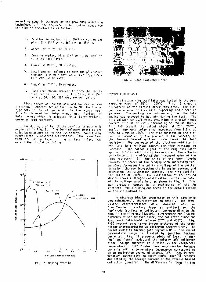
annealing step is achieved by the proximity annealingtechnique.9." The sequence of fabrication steps forthe bipolar structure is as follows:
1- Shallow Se implant (1 x 10' * cnr«!, 150 keVplus 2 x 101J-cnr-\ 360 keV at 35O°C).
2. Anneal at 350°C for 30 min.
3. Deep Be implant (6 x 1 0 u cnr^, 180 keV) toform the base layer.
4. Anneal at 800°C, 30 minutes.
5. Localized Be implants to form the p* contactregion-; (I x W'-H cnr^ at 40 keV plus 1.5 x10'" cm-^ at 30 keV).
6. Anneal at 700T, 30 minutes.
7. Localized Boron implant to forn the isola-tion reqion '2 x 10 •l, 4 x 10", 6 K 10"'cm-^ at 50, 140, 3?0 keV, respectively).
*>i3N4 serves as implant mask and for device pas-sivation. Contacts are alloyed An—fie-Ni for the n-type material and alloyed Au-7n for the p-type base.Ti - An is used for interconnections. Stripes of^aAs, whose width is adjusted by a Roron implant,serve as load resistor.
The doping profile of the complete structure ispresented in Fig. 2. The ion-implanted profiles arecalculated according to the LSS-theory, modified byexperimentally observed activations. The transitionfrom the n+ epilayer to the surface n-layer wasestablished by '-V profiling.
7 04 01 II 10 I?
Fig. 2 Doping profile
Fig. 3 GaAs Ring-Oscillator
DEVICE PERFORMANCE
A 15-stage ring oscillator was tested in the tem-perature range of 25°C - 390°C. Fig. 3 shows amicrograph of the circuit after this test. The cir-cuit was mounted in a ceramic IC-package and placed inan oven. The package was not sealed, i.e. the liaAsdevice was exposed to hot air during the test. Thebias voltage was 1.75 volt, resulting in a total inputcurrent of - mft at 25°C, increasing to 7mA at 385°C.Fig. 4-6 present the output signal at 25°, 240°C,3R5°C. The gate delay time increases from 3.3ns at25°C to 6.7ns at 385°C. The time constant of the cir-cuit is dominated by the product of the capacity ofthe forward biased emitter diode times the loadresistor. The decrease of the electron mobility inthe GaAs load resistor causes the time constant toincrease. The output signal of the ring oscillatorapprox. triples with rising temperature. Two effectscontribute to this effect:J.the increased value of theload resistor/ 2. The shift of the Fermi levelstowards the center of the bandgap with increasing tem-perature decreases the built-in voltage of the emitterjunction, thereby increasing the injection current anddecreasing the saturation voltage. The ring oscilla-tor failed at 390°C. The examination of the faileddevice shows a damaged metallization in the via holesof the voltage supply bar, as shown in Fig. 3. Thiswas probably caused by a realloying of the Aucontacts, and a subsequent break in the metallizationon the via sidewalls.
A discrete bipolar transistor on this same chipwas subsequently characterized in detail. The tran-sistor characteristics were measured both for"down"-mode (surface layer as emitter) and the"up"-mode (surface as collector, corresponding to themode in the ring-oscillator). Furthermore the leakagecurrents of the emitter diode, the collector diode andICEO w e r e determined bet.«en 25°C and 400°C. Fig.7-10 present some curve tr?cer pictures of the tran-sistor characteristics at different temperatures. Thedevice exhibits current gain beyond 400°C. The usefultemperature range is limited by junction leakagecurrents. Fig. 11 presents plots of Ir^o, in both"up" and "down" mode, and the emitter and collectordiode leakage currents at 2 volts vs the reciprocaltemperature. Both diodes have very similar leakagecurrents with a temperature dependence correspondingto an activation energy of approx. leV. Ir^o is tem-perature insensitive to about 200°C; then it becomesdominated by the leakage current of the reverse biasedcollector junction. The difference in Ir,E0 in the
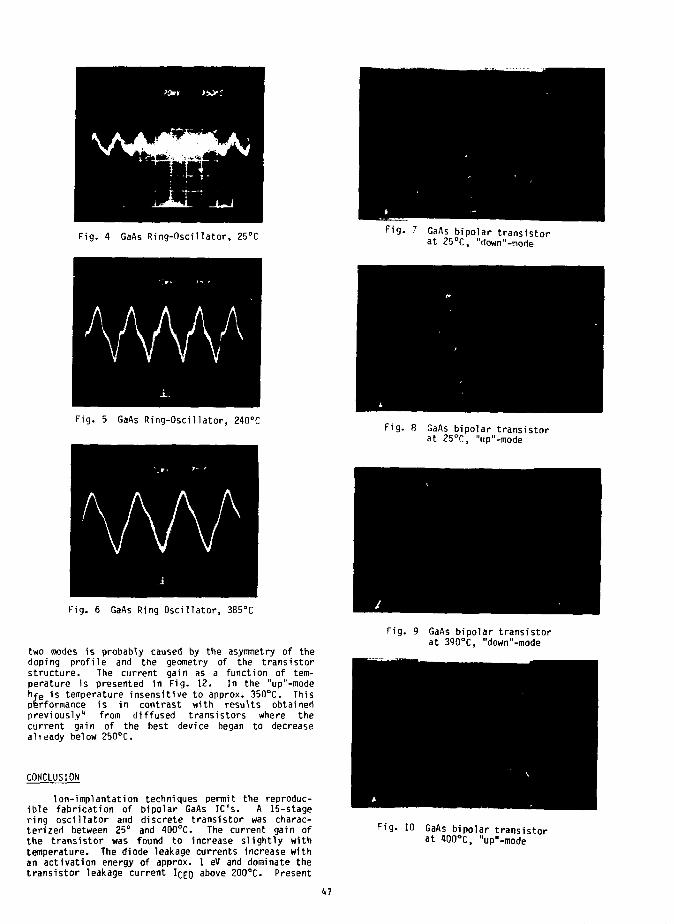
Fig. 4 GaAs Ring-Oscillator, 25°C GaAs bipolar transistorat 25°C, "down"-no(ie
Fig. 5 GaAs Ring-Oscillator, 240cCFig. 8 GaAs bipolar transistor
at 25°C, "up"-mode
Fig. 6 GaAs Ring Oscillator, 385°C
two modes is probably caused by the asymmetry of thedoping profile and the geometry of the transistorstructure. The current gain as a function of tem-perature is presented in Fig. 12. In the "up"-modehfe is temperature insensitive to approx. 350°C. Thisperformance is in contrast with results obtainedpreviously1* from diffused transistors where thecurrent gain of the best device began to decreasealready below 250°C.
CONCLUSION
I on-implantation techniques permit the reproduc-ible fabrication of bipolar GaAs IC's. A 15-stagering oscillator and discrete transistor was charac-terized between 25° and 400°C. The current gain ofthe transistor was found to increase slightly withtemperature. The diode leakage currents increase withan activation energy of approx. 1 eV and dominate thetransistor leakage current I^^o above 200°C. Present
Fig. 9 GaAs bipolar transistorat 390°C, "down"-mode
10 GaAs bipolar transistorat 400°C, "up"-mode
47
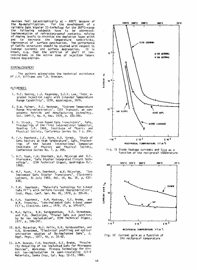
devices fa i l catastrophically at ~ 400°C because ofthe Au-metallization. For the development of arel iable GaAs bipolar IC-techology for the 350°C-rangethe following subjects have to be addressed:Implementation of refractory-metal contacts; raisingof doping levels to minimize the depletion layer widthand to decrease the temperature sensi t iv i ty ;improvement of surface passivation. The performanceof GaAlAs structures should be studied with respect toleakage currents and surface degradation. I t isknown, e.g. that the addition of small Al con-centrations to the active zone of injection lasersreduce degradation.
ACKNOWLEDGEMENT
The authors acknowledge the techn ica l assistanceo f J .A . Wi l l iams and T.B. Brandon.
REFERENCES
1 . D.C. Dening, L . J . Ragonose, S.C.Y. Lee, " I n t e : - a -g ra ted I n j e c t i o n Logic w i t h Extended TemperatureRange C a p a b i l i t y " , IEDM, Washington, 1979.
2 . D,W. Palmer, R.C. Heckman, "Extreme TemperatureRange M i c r o e l e c t r o n i c s " , IEEE Transact , on com-ponents hybr ids and manufactur ing technology.V o l . CHMT-1, No. 4 , Oec. 1978, p. 333-340.
3. H. S t r a c k , " I r o n Doped GaAs T r a n s i s t o r s " , GaAs,Proceedings of the f i r s t I n t e r n a t i o n a l Symposium,Reading G.B. 1966, I n s t i t u t e of Physics andPhys ica l Soc ie t y , Conference Series Mo. 3 p. 206.
4 . F.H. Poerbeck, E.E. Harp, H.A. S t rack , "Study ofGaAs Devices at High Temperature", GaAs, Proceed-ings of the Second I n t e r n a t i o n a l SymposiumIns t i tu te of Physics and Physical Society,Conference Series No. 7. p. 205.
5. H.T. Yuan, F.H. Ooerbeck, W.V. McLevige and G.E.Dierschke, "GaAs Bipolar Integrated Circuit Tech-nology". IEDM Technical Digest, Washington D.C.1980.
6. H.T. Yuan, F.H. Doerbeck, W.V. McLevige, "IonImplanted GaAs Bipolar Transistors", ElectronicLetters, 31 July 1980, Vol. 16, No. 16. p. 637-638.
7. F.H. Doerbeck, "Materials Technology for X-bandGaAs FET's with Uniform Current Characteristics",Inst. Phys. Conf. Ser. No. 45, 1979, p. 335-41.
8. F.H. Doerbeck, H.M. Macksey, G.E. Brehm, andW.R. Frensley, "Ion-implanted GaAs X-band powerFET's, Electron. Le t t . , 1979, 15, p. 576-577.
9. M.J. Helix, K.V. Vaidyanathan, B.G. Streetman,and P.K. Chatterjee, "Planar GaAs p-n junctionsby Be ion implantation", IEDM Technical Digest,1977, p. 195-197.
10. W.V. McLevige, M.J. Helix, K.V. Vaidyanathan, andB.G. Streetman, "Electrical prof i l ing and opticalactivation studies of Be-implanted GaAs", 0.Appl. Phys., 1977, 43, p. 33-42.
11. W.M. Ouncan, F.H. Doerbeck, G.E. Brehm, "Proxim-i t y Annealing of Ion implanted GaAs for MicrowaveDevices", Workshop: Process Technology for dir-ect ion-implantation in semi-insulating I I I -VMaterials, Santa Cruz, Cal. Aug. 12-13, 1980.
4II*C 30l"C 2II'C l l l 'C 2S*C
ICEO ID0W»)
a E l (OOWMI
o c i <oowi«:
OIOOI LEAKAGE
RECIPROCAL TEMPERATURE. 1 / T I K 1 )
Fig. 11 Diode leakage currents and IQEQ as afunction of the reciprocal temperature
«00 C 300-C 20DC
2 10 * 3 10 •
RECIPROCAL TEMPERATURE. 1 7 (K <)
Fig. 12 Current gain as a function ofthe reciprocal temperature
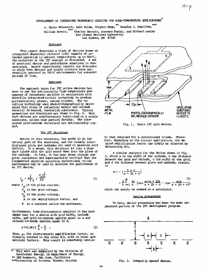
d-afDEVELOPMENT OF INTEGRATED THERMIONIC CIRCUITS TOR HIGH-TEK>ERA3URE APPLICATIONS
** *••
J. Byron McCormick, Dale Wilde, Stephen Depp, Douglas J. Hamilton,William Kerwin, Charles Derouin, Lorenzo Roybal, and Richard uooley
Los Alamos National LaboratoryLos Alamos, NM 87545
Abstract
This report describes a class of devices known asintegrated thermionic circuits (ITC) capable of ex-tended operation in ambient tsnperatures up to 500°C.The evolution of the ITC concept is discussed. A setof practical design and performance equations is dem-onstrated. Recent experimental results are discussedin which both devices and simple circuits have suc-cessfully operated in 500°C environments for extendedperiods of time.
Approach
The approach taken for ITC active devices hasbeen to use the intrinsically high-temperature phe-nomenon of thermionic emission in conjunction withthin-film integrated-circuit technology to producemicrominiature, planar, vacuum triodes. The re-sulting technology uses photolithographically delin-eated thin films of refractory metals and cathodematerial on heated, insulating substrates. Typicalgeometries and dimensions are shown in Fig. 1. Manysuch devices are simultaneously fabricated on a singlesubstrate, giving high packing density. The inte-grated grid-cathode structures are intrinsically rug-ged.
The ITC Structure
Notice in this structure, the anode is in thenatural path of the electrons, and the closely inter-digitated grids and cathodes are used to maximize gridcontrol. In a sense, this structure is like a stan-dard triode with the grid moved down into the plane ofthe cathode. In fact, it has been shown through com-puter simulation and experimentally verified that thefundamental equation governing conventional triodeperformance may be used to describe the performance ofan ITC device.
PHOTOLITHOGRAPHICALLYDELINEATED CATHODE
Fig. 1. Basic ITC gain device.
INSULATINGSUBSTRATEHEATED TO^600° c
to that obtained for a conventional triode. There-fore, depending on the circuit application, the de-sired amplification factor can simply be selected bydetermining d/a.
A similar analysis for the device shown in Fig.2, where a is the width of the cathode, b the distancebetween the grid and cathode, c the width of the grid,and d the distance between plate and cathode, resultsin
(1)
where I is the place current,V is the grid voltage,V i s the plate voltage,U is the amplification factor, and
K is a constant called the perveance.
Furthermore, from electrostatic analysis i t has beenshown that for a device with grid width, cathodewidth, and grid-to-cathode spacing equal to a andcathode-to-anode spacing equal to d.
l = _ / bt c \\a + 2b + c>
00 (3)nrfa + 2b) _ n.._a + 2b + c c o s a + 2b + c)
which can easily be summed on a calculator.
ice Processing
t = 0.5611 t - (2)
Thus, jit the electrostatic amplification factor, islinearly related to the ratio d/a/ with no other geo-metrical factors. This result i s remarkably similar
To date, device processing has been the most en-phasized portion of the ITC development program.
IJ_HlH_Lr-_
K G K G K* This work was supported by the Division of
Geothermal Energy, US Department of Energy.** IBM Research, San Jose, California•••University of Arizona, Tucson, Arizona Fig. 2. Unequally spaced device.
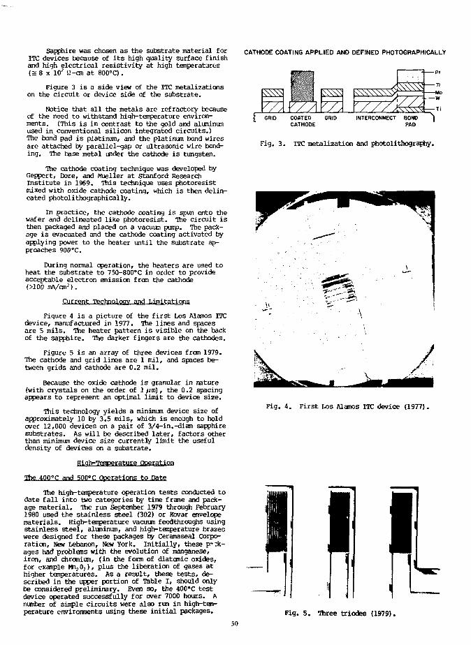
Sapphire was chosen as the substrate material forITC devices because of its high quality surface finishand high electrical resistivity at high temperatures(s 8 x 10' il-aa at 800°C).
Figure 3 is a side view of the ITC metalizationson the circuit or device side of the substrate.
Notice that all the metals are refractory becauseof the need to withstand high-temperature environ-ments. (This is in contrast to the gold and aluminumused in conventional silicon integrated circuits.)The bond pad is platinum, and the platinum bond wiresare attached by parallel-gap or ultrasonic wire bond-ing. The base metal under the cathode is tungsten.
The cathode coating technique was developed byGeppert, Dore, and Mueller at Stanford ResearchInstitute in 1969. This technique uses photoresistmixed with oxide cathode coating, which is then delin-eated photolithographically.
In practice, the cathode coating is spun onto thewafer and delineated like photoresist. The circuit isthen packaged and placed on a vacuum pump. The pack-age is evacuated and the cathode coating activated byapplying power to the heater until the substrate ap-proaches 900°C.
During normal operation, the heaters are used toheat the substrate to 750-800°C in order to provideacceptable electron emission from the cathode(MOO mA/an2).
Current Technology and Limitations
Figure 4 is a picture of the first Los Alamos ITCdevice, manufactured in 1977. The lines and spacesare 5 mils. The heater pattern is visible on the backof the sapphire. The darker fingers are the cathodes.
Figure 5 is an array of three devices from 1979.The cathode and grid lines are 1 mil, and spaces be-tween grids and cathode are 0.2 mil.
Because the oxide cathode is granular in nature(with crystals on the order of 1 fim), the 0.2 spacingappears to represent an optimal limit to device size.
This technology yields a minimum device size ofapproximately 10 by 3.5 mils, which is enough to holdover 12,000 devices on a pair of 3/4-in.-diam sapphiresubstrates. As will be described later, factors otherthan minimum device size currently limit the usefuldensity of devices on a substrate.
Hiah-Temperature Operation
The 400°C and 500oC Operations to Date
The high-temperature operation tests conducted todate fall into two categories by time frame and pack-age material. The run September 1979 through February1980 used the stainless steel (302) or Kovar envelopematerials. High-temperature vacuum feedthroughs usingstainless steel, aluminum, and high-temperature brazeswere designed for these packages by Ceramaseal Corpo-ration, New Lebanon, New York. Initially, these p l -ages had problems with the evolution of manganese,iron, and chromium, (in the form of diatomic oxides,for example ttijOj), plus the liberation of gases athigher temperatures. As a result, these tests, de-scribed in the upper portion of Table I, should onlybe considered preliminary. Even so, the 400*C testdevice operated successfully for over 7000 hours. Anumber of simple circuits were also run in high-tem-perature environments using these initial packages.
CATHODE COATING APPLIED AND DEFINED PHOTOGRAPHICALLY
{ GRID COATED GRIDCATHODE
INTERCONNECTBONDPAD
Fig. 3. ITC metalization and photolithography.
Fig. 4. First Los Alamos ITC device (1977).
Fig. 5. Three triodes (1979).
50
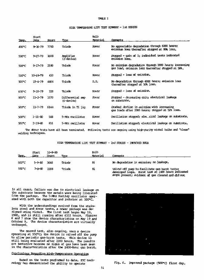
TWT.F. I
HIGH 1QFESKIURE LIFE TEST SUMBFDf - 1 s t SHOES
StartDate Hours
BulbMaterial Qinmits
400°C 9-26-79 7750 Triode
500°C 9-27-79 1608 ftiplifier(2-device)
500°C 9-17-79 2590 Triode
Kovar
Kovar
Kovar
500°C
500°C
600°C
500°C
500°C
500°C
500°C
10-18-79
10-4-79
9-20-79
11-2-79
11-7-79
1-31-80
2-19-80
430
4464
328
1070
6144
588
816
Triode
Triode
Triode
Differential anp(6-device)
Triode in Ti j i g
5-Mfc oscillator
5-fflz oscillator
Kovar
S.S.
Kovar
Kovar
Kovar
Kovar
Kovar
The above tests have a l l been terminated,welding techniques.
NO apprecixfcle degradation through 6000 hours;emission loss thereafter stopped a t 80% loss.
Stopped - gain of 1; individual t e s t s indicatedemission loss.
No emission degradation through 2000 hours; increasinggas load, emission loss thereafter stopped a t 50%.
Stopped - loss of emission.
No degradation through 4000 hours; emission lossthereafter stopped a t 50% loss.
Stopped - loss of emission.
Stepped - decreasing gain; electrical leakageon substrate.
Gradual decline in emission with increasinggas loads after 2000 hours; stopped a t 50% loss.
Oscillation stopped; elec.rical leakage on substrate.
Oscillation stopped; electrical leakage on substrate.
Following tes ts are ongoing using high-purity nickel bulbs and "clean"
HIGH TEM'ERATURE LIFE TEST SURREY - 2nd SERIES - IM9HDVEO BULB
1*51?.StartDate
10-8-80Hours Type
BulbMaterial Qmnents
500°C 5-9-80 3648 Triode
550-C 7-8-80 2208 Tricde
Ni No degradation in mission; no leakage.
Ni Valved off pump to facilitate gas burst tests;developed loops. Burst test at 1400 hours indicatedargon present; evidence of gas cleared and did not
In all cases, failure was due to electrical leakage onthe substrate because the metals were being liberatedfrom the package. The 5-mz Hartley oscillator oper-ated with both the capacitor and inductor at 500°C.
With the understandings evolved from the stain-less steel and Kovar tests, a newer package was de-signed using nickel. The first test began May 19,1980, and is still running after 6312 hours. Figures6 and 7 show the device characteristics on May 19 andOctober 9. The device characteristics are virtuallyunchanged.
The second test, also ongoing, uses a deviceoperating at 550*C; the device is valved off the pumpto allow periodic gas-burst tests. This device isstill being evaluated after 2200 hours. The resultsare tentative because no signs of gas have been seenin the characteristics after the 1400-hour gas burst.
Conclusions Regarding High-Temperature Operation
Based on the tests performed to date, ITC tech-nology has demonstrated the ability to operate Fig. 6. unproved package (500*C) first day.
51
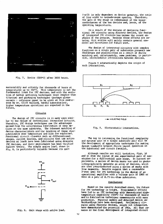
Fig. 7. Device (500°C) after 3600 hours.
successfully and reliably for thousands of hours attemperatures up to 500"C. This temperature is not thefundamental limit for ITC devices, and with the evolu-tion of better gettering techniques (more complex thantitanium) and packaging techniques (perhaps glass-ceramic - reference paper to be given at this confer-ence by Dr. CLiff Ballard, Sandia Laboratories),higher temperature operations are expected in thefuture.
The design of ITC circuits is in many ways simi-lar to the design of conventional integrated circuits.Therefore, ITC design techniques use the advantagesgained from the simultaneous fabrication of many de-vices on the sane substrate. The inherent matching ofdevice characteristics and the tracking of these char-acteristics over temperature and life are exploited.Functional circuit elements such as differentionalstages, current sources, and circuits that use activedevices as loads have been fabricated using discreteITC devices, and their performance has been verifiedagainst theory. The simple active load, shown inFig. 8, is particularly valuable because its gain
+V,
_Louti
(-«/2) is only dependent on device geometry, the ratioof line width to cathode-anode spacing. Therefore,the gain of the stage is independent of the trans-conductances of the two devices and, hence, of theoperating temperatures.
As a result of the success of designing func-tional ITC circuits using discrete devices, the designof integrated ITC circuits has become the recent em-phasis of the program. Because these efforts are on-going, this section will mainly contain general com-ments and directions for future work.
The design of integrated circuitry with complexfunctions on a single pair of substrates presents newchallenges and possibilities as a result of devicematching and, unfortunately, some problems, in partic-ular, electrostatic interactions between devices.
Figure 9 schematically depicts the origin ofsuch interactions.
G, K,
Fig. 8. Gain stage with active load.
• = ELECTRIC FIELD
Fig. 9. Electrostatic interactions.
The key to increasing the functional complexityand maximum gain on a single substrate pair will bethe development of appropriate techniques for makingdesign tradeoffs between device layout (position onthe substrate) and circuit function.
Although results are still tentative. Figs. 10and 11 show the layout of one experimental pair of sub-strates for a differential gain stage. In current ex-periments, a series of device masks are used to photo-lithographically generate an array of devices, whichare then interconnected using a series of masks withline segments. Results suggest that a reasonable2-year goal for rrc technology is the design of anoperational amplifier with a voltage gain of 1000 ormore on a pair of 0.75-in.-diam substrates.
Conclusions
Based on the results described above, the futurefor ITC technology is bright. Programmatic effortshave led to an ITC technology with demonstrated high-temperature capability (500*C for thousands of hours)and to fabrication techniques commensurate with massproduction. Physical models and detailed device un-derstandings have been developed. Preliminary cir-cuits using discrete devices, single not integrated,have demonstated the potential of ITCs. All that re-mains is the final development of integrated circuit
52
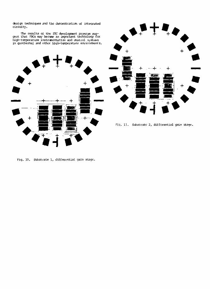
design techniques and the demonstration of integratedciccuity,
the results of the ITC development program sug-gest that ITCs may become an important technology foehigh-tanperature instrtmentation and control systemsin geothermal and other high-temperature environments.
_ ~ ^
••4 • •Fig. 11. substrate 2, differential gain stage.
Fig. 10. Substrate 1, differential gain stage.
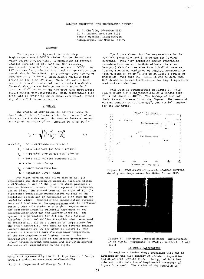
GALLIUM PHOSPHIDE HIGH TEMPERATURE DIODES*
R. J. Chaffin. Division 5133L. R. Dawson, Division 5154Sandia National LaboratoriesAlbuquerque, New Mexico 87185
SUMMARY
The purpose of this work is to develophigh temperature ("-300 C) diodes for geothermal andother energy applications. A comparison of reverseleakage currents of Si, GaAs and GaP is made-Diod .-? made from GaP should be usable to ">500 C. AnLPiC process for •, reducing hiqh quality, grown junction'lap diodes is described. This process uses low vaporpressure Mg is a dopant which allows multiple boatgrowth in the same LPE run. These LPE wafers havebi^en cat into die and metallized to make the diodes.These diodes produce leakage currents below 10"J
A/cm- At 400 C while exhibiting good high temperaturerectification characteristics. High temperature lifetest data is presented which shows exceptional stabi1-ity of the V-T characteristics.
I THEORY
The figure shows that for temperatures in the20-300 C range GaAs and Si have similar leakagecurrents. (The high depletion region creneration-recombination current in GaAs offsets its widerbandgap.) Calculations show that GaP diode reverseleakage should be dominated by generation-recombina-tion current up to 650 C and is at least 5 orders ofmagnitude lower than Si. Hence it ca*i be seen thatGaP should be an excellent choice for high temperaturesemiconductor devices.
This fact is demonstrated in Figure 2. Thisfigure shows a V-I characteristic of a Sandia-madeP+ -N GaP diode at 400°C. The leakage of the GaPdiode is not discernable on the figure. The measuredcurrent density at -3V and 400 C was 7 x 10""" amp/cm-'for the GaP diode.
The choice of semiconductor material used tofibricate diodes is dominated by the reverse leakagecharacteristics desired. The reverse leakage currentdensity of an abrupt P+ -M junction is given by:''-
R
Hf n*: en. W
I T N 2T1 p D o(1)
Si Measured *•«
Gap Measured-x
D
- hole diffusion coefficient
= hole lifetime (in the n region)
~ depletion region carrier lifetime
= intrinsic carrier concentration
= electronic charge
= donor concentration
h = depletion layer width
The first term on the right side of Eq. (1)represents the diffusion of minority carriers witnina diffusion length of the junction which produces areverse leakage current. This component is independ-ent of bias. The second term on the right of Eq. (1)represents generation-recombination current ii. thedepletion region and is dependent on bias through thedepletion width. Generally the recombination currentterm will dominate at low temperatures 3nd the diffusioncurrent term will dominate at higher temperatures.The crossover point is primarily dependent on. thesemiconductor band gap and carrier lifetime. Theappropriate parameters for Silicon (Si), GalliumArsenide (GaAs) and Gallium Phosphide (Gap) were usedto evaluate Eq. (1) as a function of temperature forthe three materials. The results for reverse leakagecurrent density at -3V are shown in Figure 1. Thearrows on the curves mark the crossover temperatureof the two components of leakage current. Fortemperatures to the left of the arrows generation-recombination current dominates and diffusion currentdominates at temperatures to the right.
*This work sponsored by the U. S. Department of Energy(D.O-E.) under Contract DE-AC04-76-DP00789
A, U, S. Department of Energy facility.
Figure 1. Comparison of reverse leakage currentdensity vs. temperature for GaAs, Si and GaP.
Figure 2.Q Gap grown junction diode characterist-ic at 400 C. (Horizontal = 5V/div, vertical = 1 mA/div.)
II DIODE FABRICATION
To realize a device whose operation will not bedegraded by the high density of chemical impuritiesand structural defects present in typical bulk GaPsubstrate material, the all-epitaxial structure ofFigure 3 is used. The N side of the junction is
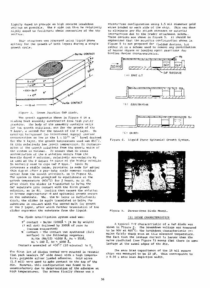
lightly doped to provide as high reverse breakdownvoltage as possible. The P side can then be relativelyhighly doped to facilitate ohmic contacting of the topsurface.
This structure was prepared using liquid phaseepitaxy for the growth of both layers during a singlegrowth cycle.
B«/Au CONTACT
AurtSe CONTACT
stress-free configuration using 1.5 mil diameter goldwires bonded to each side of the chip. This was doneto eliminate any die attach stresses or materialinteractions due to the header attachment schemt.These devices are shown in Figure 5. It should beemphasized that the mounting configuration shown inFigure 5 is not proposed for fielded devices, butrather it is a scheme used to remove any contributionof header stress or bonding agent reactions fortesting device characteristics.
Ga-P
I A ) BAKE OUT-GaP SUBSTRATE
I B I EJUILIBRATIUN
Figure 3. Grown Junction Gap Diode.
The qrowth apparatus shown in Figure 4 is asliding boat assembly constructed from high puritygraphite. The body of the assembly contains wellsfor two growth solutions, one for the growth of theM layer, a second for the growth of the P layer. Tomaintain background (no intentional doping) carrierconcentration as low as the 1 :•: 1016 cm"1 level desiredfor the N layer, the growth temperature used was 850^C.At this relatively low ;rowth temperature, Si contamin-ation of the growth solutions from the quarts walls ofthe system is minimal. To ensure that no crosscontamination of the N solution occurs from theheavily doped P solution, relatively non-volatile Mgis used as the P dopant in place of the highly volatileZn normally used to dope Gap P type.3 Since Mgpossesses a stable oxide, provision is made for addingthis dop/nt after a pre- bake cycle removes residualoxygen from the growth solutions, as in Figure 4A.The system is then permitted to equilibrate at thegrowth temperature (850 C} for 2 hours, as in 4B,after which the slider is translated to bring theGaP substrate into contact with the first growthsolution, as in 4C. Cooling then causes the solutionto become super-satura* i'd and epitaxial growth occurson the substrate. Wht.. the N- layer is sufficientlythick, the slider is again translated to bring thesubstrate in contact with the second melt for growthof the p layer, after which further translation of theslider separates the substrate from the liquid.
The diode metallization system used was:
P+ contact - Be/Au (3000A i» 1% Be by weight)(7 mil dot) followed by 3000A of pure Au
(vacuum evaporated)N contact - The contact was sputtered (full
surface) in the following sequence:Au/Ge (88/12) V1000 A, Au T. 250A,Ni a. 600 A, Au "V 4000 A,
Contacts arcnealed at 450°C (10 minutes) in H
The first lot of diodes tested were mounted in ceramicflat pack headers (N+ side down) with a high tempera-ture, polymide silver loaded adhesive. Gold wires(1.5 mil) were used to make contact to the top of thedie. However, this configuration was found to beunsatisfactory due to deterioration of the adhesive athigh temperatures. The scheme finally chosen was a
s / / / 7^
I C i GRUWTH
Figure 4. Liquid Phase Epitaxial Growth System.
Figure 5. Stress-Free Dioda Mount.
Ill DIODE CHARACTERISTICS
A typical I-V characteristic of a Gap diode wasshown in Figure 2. The breakdown voltage was measuredto he 90V at 400°C; the breakdown characteristic re-mains fairly sharp even at this elevated temperature.The fact that the leakage current is larger than thevalue predicted (see Figure 1) means chat there is someleakage at the sawed edges of the die.
The zero bias capacitance of the 15 mil squarechips was measured to be 22 pP. This corresponds toa 0.56 u zero bias depletion width.
56
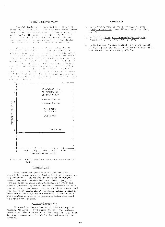
IV KMVIHV-'NMLSTMI. TE:'T.'
1 . A.
REFERESChS
Pliys i c s and T ^ c h
rh<.- J i ^ i c . v.vr<' : 1.K--.-<} i n o v e n s a f
-\ . •<• w< :- :: ;T , . - t i H"i .Kid t h e ovi.-:.
tuyx;-. f 1 S c r . i -
K , I ) . i v sou , " ' )op in>; C o n t r e 1 in i lu- U Y w r o v t hr, . i : '" , (i.ipc-r pr< ^ i u w ! ;\t t' I t e i r o n i c s *-l;i*L t.-r i . i l .
/ f , ( o r n . - l 1 I ' n i v . , ' V ' ^ / S O .
L . - . . ; • l . : : .
* i : • i : . ; .1
2 0 0 400 600 800TIME — HOURS <af 300°C)
E'i jure G. }Q0 -' Li fu Test Data on ;: tr -ss free GaiDiodes.
V C'OIJCLUSIOHP
This paper has prt;-s*-ntud dat i on (jallium-i hosphide, qrown junction diodes for high temperatureapplications. Information on fabrication methodswere presented. Evaluation data shows: good lowieakaqe rectification characteristics at 400 c andstable junction and metallization parameters at 300 Cfor at least 1000 hours. The onLv problem encounteredwas the "high temperature" polyimide adhesive used tobond the diode chips to the headers. A now cuteticchip bondinq procedure is presently being developedto solve this problem.
VI
This work was suppor ted in pa r t by ihu Hope, ofEnergy, D i v i s i o n of Ceothermnl Energy. The . lutl inrswould a l s o l i k e to thank I. 15. S n e l l i n ^ and T. A. P lu tfor t h e i r a s s i s t a n c e in t.ibr ic.it ing ,-ind t e s t i n g thed e v i c e s .
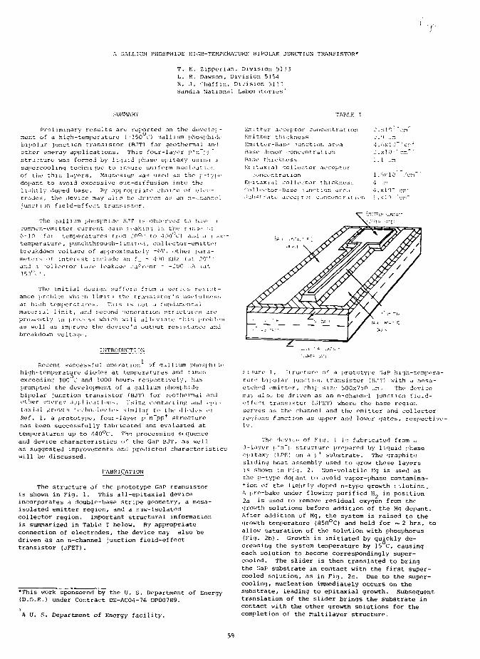
GALLIUM PHOSPHIDE HIGH-TEMPERATURE BIPOLAR JUNCTION TRANSISTOR*
T. E. Zipperian, Division 513 3L. R. Dawson, Division 5154R. J. 'naff in, Di/ision 513-Sandia Nationa 1 Labor ltorms*
.SUMMARY TAELK T
Preliminary results arc- reported on the develment of a high-temperature ( • 350 C) qal 1 m m phosphbipolar junction transl stor (BJT) for geothermal aother eneray applications. This four-layer prn ;•:strujfjrc was formed by i l^uid pnaso epitaxy us m osupercool inq technique to insure uni form nucleat uof the thIn 1 dyers. Maqr.eslurn was used as the p-1dopant to avoid excessive out-diffusion into theluihtly doped base. By appropriate choire of electrodes . the dev ice may J U O be dr i von as an ri - c ri anjunctIon field-effect trans istor.
r.q in the ran ?••to *i00°C) and
The gall lum phosphi de B,TT iscommor.-emi tter current qain ; i-akir6-] 0 ' f oi temperatures from JlOtemperaLure, punchthrough-1uiu te.i, colleetor-unitto:breakdown vol taqe of approximately -0>V. . it her para-meter^ of interest include an f^ = 400 KHz (JL 20° "•and .i .-oi lector 1 ase leakage current - -J'JO .-A ut
The initial desiqi. suffers from a set les rv.-=\ st -ance probler whi ch 1 inut s the transistor ' s usefulnessat hi-;h temperatures. Th 1 s is not a f undam<_-nta imater ial limit, and second '.'enoratior. struct JL os arepresently in process winch wi 11 al leviato t-hi s problem
breakdo^Ti voltaq- •.
INTRODUCTION
Recent successful operation ?f qallium phosphi i«-high-temperature d iodes at temperatures and t lme.sexceedinq 300 C and 1000 hour^ respectively, hasprompted the development of a gal 1lum phosphidebipolar junction transistor (BJT) for qeothermal andother ener^v appi ii'.it i<ms. Vsin^; •.ont.ut inj; .nul i-pi-tax i,il >;r,iwti! ' ci-hnul m: i e.s similar to t he d iodes o\Ref. 1, a prototype, four-layer p n'pp* structurehas been successfulLy fabricated and evaluated attemperatures up to A40°C. ^'-in processing sequenceand device characteristics o r the GaP BJT, as wellas suggested improvements and predicted characteristicswill be discussed.
FABRICATION
The structure of the prototype GaP transistoris shown in Fig. 1. This all-epitaxial deviceincorporates a double-base stripe geometry, a mesa-isolated emitter region, and a saw-isolatedcollector region. Important structural informationis summarized in Table I below. By appropriateconnection of electrodes, the device ma> also bedriven as an n-channel junction field-effecttransistor (JFET).
*This work sponsored by the U. S. Department of Energy(D.O.E.) under Contract DE-AC04-76-DP00789.-i-
A U. S. Department of Energy facility.
lini titur acceptor concer.trat ior. 2 .:: 1'-'Kmi tter thi ckness j. CJ ,,nHmi tter-Has-• i unction area •',. G>:1 jBase joiior •.•onct-ntrat ur. J.xlO' 'Hase thickness 1.1 ..nK:itaxial collector acceptor
.roncer.tration 1 . rj:-:l0 •Epi taxi a 1 col lector thickr.esi, A -mr'ol lector-Hase iun<"t ion area •*.. xlO".vjib-str.ite acceptor •jjRCi.-ntrjticr. l.x:^-
r i-;ure 1. .-'trurture of a prototype GaP hi'jh-ternpera-ture bipolar iunction transistor (BJT1 with a mesa-etched emitter , chip1 size 500x750 ..n . The dovi ~ema> alsu be driven as an n-channel junction fieid-effect trans is tor (JFET) where the base reqior.serves as the channel and the emitter and col lectorregions fanctinn as upper and lower qates, respective-Iv.
The -lev ice of riq. I i •; fabricated from ^3-layer p+n~p structure proTjared by 1iquid phaseepitaxy (LPF) on a p+ substrate. The qraphi t*islidinti boat assembly used to grow tliese layersis shown in Fi;. 2. Non-volatile Hg is used asthe p-typc dopant to avoid vapor-phase contamina-tion of the liqhtly doped n-type growth solution.A pro-bake under flowing purified H^ in position2a is used to remove residual oxygen from thegrowth solutions before addition of the Mg dopant.After addi tion of Mg, the system is raised to thegrowth temperature (850°C) and held for — 2 hrs. toallow saturation of the solution with phosphorus(Fig. 2b). Growth is initiated by quickly de-creasing the system temperature by 15 C, causingeach solution to become correspondingly super-cooled. The slider is then translated to bringthe GaP substrate in contact with the first super-cooled solution, as in Fig. 2c. Due to the super-cooling, nucleation immediately occurs on thesubstrate, leading to epitaxial growth. Subsequenttranslation of the slider brings the substrate incontact with the other growth solutions for thecompletion of the multilayer structurn.
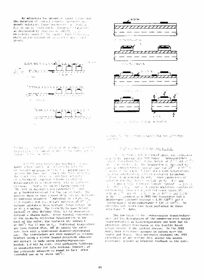
By ad Justin:.- the amount othe dura t ion of .rent .i^t i ' - t w egrowth so lu t 1 or., 1 ivt-r 'jii,-.*::;-0.2 .-n -:an be ->::t r-,i1 •• : . Tr.ras J e l ineat-^d ty . . U i : :;>: i:. t
excel lent . owin: r. - :.* , J : er •
I
i l l " h r -•• r
met J 1 i zd!. ion ry -st.-t
as a ntasKinu mat I T I a 1 ' • "i" the Gai --t w.tr.t. . Tr,-
enittt-'j mesa is the:; r >rncd J F '<"?. sr • i "• -r:- r> i .-a i -
ly remcviri'; unwant-r.1 mat^r ial i."- i r' ,'-' • ,'• (,
! ).r> molar;: KoH (1-; r.r.lar) solution at 1" .
Wi thout agi tat i'jn this mixture .-t i.L-? ; -t/p* ;a'
at 80 * R nm/rnin. The t----Ge 'Si ,'Au base it".,i 1 -
ization is then defined (Fig. Sc) by deposit :«>:.
through a shadow ^iask. After thermal ••vaporatio:.
of the Au-Be/Au collector r.etal lzatior; or. the
back of the wafer, the contacts arc inr.eaKJ
at 500'f for 15 min in H^. Individual transistors
are then forwed (Fiq. 3dT by sawirw the rfafer
intc; dice with a hiqh-speed diamond-in:>reanated
saw• The transistors are then mounted in ccrraic
headers using a silver loaded poiyinide adhesive
and contact is made using therr.ocompression-
bonded, 1-0 mil Au wire. This packaging technique
is unsatisfactory for life testing, however, as
the polyi.iude adhesive is known to fail after
extended use at or above 300 (.*.
i :•:-] :r:r. :, , . i l, ;-t."r-t-n 11 r cr fcreak.iown
-: .i: ; • • >>: jr.it • Iv -<-V. ' thc-r : arar.rt^r s o*
anj'lif lor :-on?t
rwt-r ':.ii TV, of :
eratfd as a JFE7 the transistor had aage - l.SV (20°ri and a
si r-j -1 irt
trans conductance = 120 -..H (20w) .tt-sts :;avt- been per formed on thesdate ,
.-•-ur
: roin
The 1 ow va 1 ae <;: the "omoK-source transconduct-
.i.*id the dcjradut 10:1 of the conmon-eir.i tter output
r t e n sties at h L ih-ton::erature are both due to
? i v :ori-.'s re si stance ir. the lightly doped
- ru-nior. ,: tht initial design. In *-he JFET
this •-.-•••istanci appears in series wn'i the
c and ira.::. This seriously degrades the JFET
rties .is any vnit,jQf riror across the source
tanr* J; ; t-.irs as negative feedback on the gate.
6fi
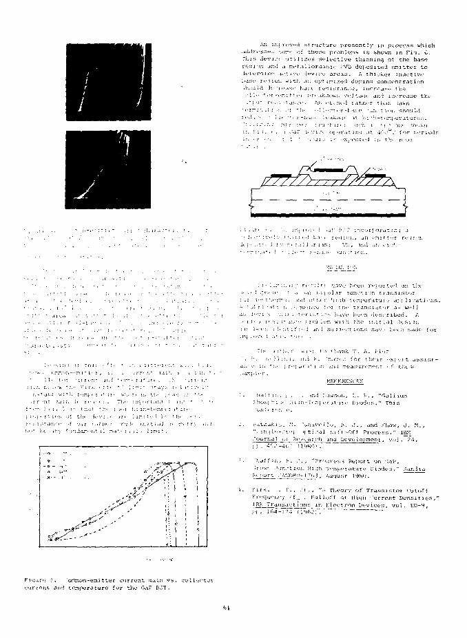
An lrti-rovd structure presently in process whichjddrosse.s sor.r of tho;;<i problens is shown in Fig. C.Tr.xa ticvi.> u t i l i zes selective thinning of the baserwiDji .*::<: ,, rft;i] 1organic rVD doj-osited emitter toit; tt- m 1 m- a---'. 1 v<_- i^v ; i_- arc AS . A th i cker i nact ive'.jar,*- r--*3ioi. w i i h j r . oiiinu concentration
;*; •.•' f.-ii.,: j r . . : i ' . An d , r,i->: : a t h e r th<ir; ; ;avn' c;"~ : : . : t : , j . > -* t in- -<•-,' 1 • %-* (<i -i-!t:;f' ^urr;'. ~.or. s h o u Idr r , i , - . • ] i . •'.;-•,._,,.• l f . ikcKj ' .it h i ' i i - t , L T r o r i t ' . i r < . - : i .' • • : : - ' - * • : "-~.* -•- ' / • ' : ; r . j - t u ; . :. . u-.*i. t- * r 1 ori*. ^h-'>v.-n-:. >• i ; . • . i •."•ar i r . ' u v at . u r . i t U J I ; j t -iO')wC" f o r : , t*r:
]
.'.;'•' : i . j ! a . " " ' i , : : :;r - * . '.:. :ru i'/.-- : '.^i' h."V ir.corj oyatz;;1? _i- I*---* ; V-- ] v ' :.i :.:;•••: h.i: -• r (" i io : . ( an or.: T t -.;r r .."•
. r • • ' . : ; • - i : • : • i • • . •• ' • •> ' ' •
: ' , ' • • : a i v i i . '• * . • • " : • i ; < ' • ••' ' i ' '.
r j - ' t . i , . L t i . • T • • . • i • : , ; t s : • • • • t . - ' • , •
'. i. • - ' . i :\ i i t f f u : • * r • * . • J : i r : < • : • : . • •«
.^-A-, t , - r r . : i . - i - ' n i M - - ! , i . . - i r r ^ ; . • : . n : . i
• r i - T i t u i ; . ;• •:<.• i-_-* • , T i . - - - . T . ; ' ^ r ? , » : : ' : i t . '
. r , • : : . ' j i r i h - i t * h < ; • • ) - ! h : ; h - t . - n : . •: i t : x
i : • : i r . ; : . t: V r f . T u l r : CV.Y 1 ijoor: r t r j o r t > - ' ; on t h r: • ' . • 1 .Tr^.'-M* r .j \,Vi i . i j o i - i r T u ; ' . c t i - ; n t r . l r . s i . s l o :
A ? j i ; ; •.!' : :. •• ;Ui.-:;ctj S">i t i n - t r a n s i s t o r ,5s Weil
.•'•z :•• , :>:;i.;' t : . . - - t r o i ] - . n w i t h t h e i r . i t i a l . 5 .u^ i - : : :
-. c . :•••<•;. : :. :,t : : ' : • : JJ . i .s;j : j*-.st l o r u ; h a v . > b e ^ r . r . a d f f o r
" h . i-.tU-.r. ' . - . « . !••• t l i n n ; ; T . A . M > j t
•• ! - . : . • ) ! : : . : . ..1..5 V . ^ . i v . - . - . f o r t h e i r - x ; t - r t a s s t a -
RKFEKE.WB.1-:
iUit.-aKiu.. :•'.. .".in.jvfJ j/>, ••.. . : . , and shav.-, j . M."- ill 1 l'--."f: 1: t i r a l Li f t -of f P rocess , " IBM.'ournaJ 01 Re:-;vaiJch anci Dove- iofCTent. vu] . 2'1,j j . 4r:;'-.i(1 U'.'ROi . ~
haff i : . , K. . T , , "Proqre^s Ruport on '~,at',•")•". ' 'Jr,rtio.\ liiijh T''n;.icratur<;- Dicxii-s," ,-dridla
v-i Port . ,\::PH'.I- 1 "fa i , Airjusr 19H0.
-'irk, . r . , . ' i . , "A Ti.oory of Trtinsi.stor cutoffr rcqu'jucy (f __ j K.illoff a t iliqh 'urront Dens i t iesIPJ- Transar:tions m Klcctron Deviec-K, vo l . t'D~^,
Ti^urt; 5. "orc^or.-enitter current qani vs. cocurrent, and ternperature for the G,iF BJT.
andi r
wt r i
t
i i
h i
I t
i:i r
r
worke andrt'i r . u
t'sst'C*
W u
i ntoun
S U
! orr v
d e r
nUltTt.i-fU
i a t i ' i n a b i
• a u - M i ' S / l
, o n d i t i " i
t
H I
[. J-
• ^
O
t
s .
RELIABILITY STL'DY OK REFRACTORY tiATE GALLIUM ARSENIDE MESFETS*
John C.W. Yin and William M. Portnoy
Department oi Electrical Engineering
Texas Tech L'ni vers i ty
Lubbock, Texas 79409
Summary way of striplines patterned in the nickel. The con-
nectors accomodate two fixtures side-by-side; a
t-! rac tory ga . e MFSf-TTs have been ! abr i i. a ted as sta i nless steel tray holds fourteen connectors, so
•J r:I.J t i ve 11- i! um i nun gate dev i c es , wh i ch have tha t up to twenty—eight devices can be stressed siniul-
Mind t .i he unre I iah 1 e as !\I power .imp 1 i 1 i er^ . taneousl v. The temperature test chamber is a 315 "C
I . at-: 1 i t y oi t i.e neu st rui t. ures has no* vet inert gas oven conf igured for nitrogen flow. A three
inch diameter t <-fcd through port, capped with a PTFE
;eedthrough, completes the test chamber arrangement.
A i lu-rn;.'; ouple measures the temperature at the geo-
n;«-irii tent er oi t he tray at sample height.
t .-r.perat-i! . ami i.rv.ird gate ujrrfiit to enhance ] he devut-s were stressed electrically at two
: . ; r. -•.:, i •- o! w, • r V it I 'iO i ,nu; J /1 C <i re L hanne! L eir.pe rat ures, 150 C and 27 b C. Electrical
i ••<• :,'•:• . -.tress lon.sisted oi biasing each device near 1. andh ass
J r i v i iig t he ga* e i nt o I orward cond ition, in some cases ,
_• L quit* heavily. The devices could not be biased at the
, . . . , ri.ir.L v.i! lit1.1! . •: I , , and s imultaneouslv at t he same
;.L : : : e %-i: l 1 •. , t :;t -.en. i,. . ndui t > • i nulustrv met a 1 iiss
.i r ' . r '"• .L • : ! • a:- r l. at i« TI was a 1 um i nun., par- c r.i i i;->oui\ «.- vo 1 tages , because oi their di f I e rent
>:'.•• i -•! ::-.<. gat t . .in re 1 ia;u 1 i t v o: a i uiriinur. i tiaracter ist it s ; in order to maintain equal DC channel
. , . . . . , . . . 1-10 :'ower di ss iiiat ion, and equal channel temperatures fori l . ' e i : X l ^ : l I - ! l . i > f e e l l i X t t - I l s 1 V e 1 V s t u d i e d , ' , ' . . * ^ , , ,
, , . . . . . . . a l l d e v i c e * , u u r i r i r s t r e s s , t h e d e v i c e u - i t h t h e l o w e s t. r L.i M. ! a i 1 a r e T:.ei h.*:ilsn:> b.lVe b e e n i d e l l t 1 I l e d , , , • ' , ,
1 , c u r v e (\ = 0) was b i a s e d a t t h e i n t e r s e c t i o n:.*.'. ] ' . . i . / ! in I : ur. i tiuir. u,i I e me t a 1 1 i / a t i on . I tie I;>M gs.i::-.'-rt mt : tiie-^i a r e ah i r i p . u r . » 1 ec t rc ir, i g r a t i on «•: t h e load l i n t and t h e I , c u r v e and t h e o t h e r
, - . , d s sir.-t. i: iruiir r f i a^ i l o r n . a t i o n . ! rie ! a l l u r e p r o b - , ,
; '. 1 i ; j . , • Ms s i • •• i i .lev 11 e.-. i a t t he same c h a m b e r t e m p e r a t u r e ) w e r e D i a s c a' " ' ' ' * ' ' * . ' ' ' . ' . '. a t a d r a i n c u r r e n t e q u a l t o t h a t v a l u e oi I , . For
:l e MM*, t I,- a i utr-1 imm ga t e i s be m g a h a n d o n e t i , d s sr. : r .-.v i , rv g . i t t i s ix - i : ^ : i n t r o d u c e d i n i t ^ e q u a l l o a « l i n e s , a l l d e v i c e s t h e n w e r e b i a s e d a t t h e
: • i - / a l t • I'n-, i - t - wt a r e t r a i t o r v m e t a '.: k\ . >:il i. t a:n! a i o n d u c t i n g j;o 1 d iiieta 1 I i z a t UM
i t
s . m
a
a lci
r a l n
lo.KiU i e s t
W e r e
l '
!
"e
b
ur re
i lies
nt v
i a s e
• n t i
, a la lue
d be
•(j
1
I
ua i
deo i
OW
V
\"
t
ret rai t o rv meta'. .init- qu ie scent v.i lue o! V . Al though the other de-
. . . , vi, f-, were biased below their I . values, forwardiL to provide metal- ass
i irpi'.i! •-1 a':- i 1 i t •• ; I he must <. ommon re! rat torv gat e ga t e cur rent I lowed for sul f ic ient posi t i ve gat e-
: -. t. i t. i:.; n::.-j' Lit iiuii;.-,-. Id. 1'iie re 1 i.ib i 1 11 v oi re t rac- sourt » vo 1 tage swing. The gate-sour co vol tage swings
t "iv i'.itc "h^ I I 1 - has been assumed to be better tli.in were set to prov ide equa 1 dra in-source vol tage swings,
tiiat . • i a ; un: inur. t;at -. MKSKK'I s . However, e 1 ei t ro- in order to obtain the same AC channel power dis-
, , 1 1 - l J , . . si pat i on.:: ; j.' r.it i,-r. Mas ;-eeii onser ved m go Id ant! l n t l ta-
, i he out put rvs i stance oJ tbe NtSrET becomes nt*ga-
r,: um-i-i> 1 ii ' I ; , n.s, an<i t ai 1 \ire modes in ret rac tory t i ve at certain values oi the drain current and drain-
.it e dev i i es sini !,ir to t hone in a I urn i num gat e dev ires source vo] tage . It the load 1 ine passes through a
art possible. I'h i s work was undertaken to obia in reg ion oI device negat ive resistance, there is a con-
si.it i->Ui .i ''ii : a i 1 ure 11 r and to det ernii ne t a i 1 ure s iderabl e poss ihi 1 i ty of osci 1 lat ion , so that the
tTii des -! re: r,u torv gate "IKM'RTs. drain resistance must be such as to limit operation to
a safe region, that is, to a region of posi t ive output
r >.J.1t_rJj| c_i_1t.a ] f'rjn^Jjire res is Lance. 7'he safe value of t)-e drain resistance is
obtained by drawing a load line which begins at the
I'iie MhSKKT used in this work is the Texas I nst ru- d ra in bias vol tage on the V axis and which crosses
Dents MSrid I gallium arsenide transistor in the strip- , , ,, , - , i J i • • . tfu' ' > curve ai its corner, just below the point at
line package. hach packaged chip consists o! two dss * J p
i nd i v i dua1 cells, each cell deli ver ing 2 SO mW of micro- wh ich the output resistance becomes negative. This
uave [lower at 8 ilH/.; on 1 v one of the cells is used in v.i 1 ue is, of course, differ en t for different devices,
t!ti- MS80 I . N'eirma 1 1 y, the chip is sealed in epoxy for and even for a single device at various temperatures,
protection; however, the epoxy fails near J00 'C, so ] decreases with increasing temperature; for a
t iuit the devices tested lie re were unencap.su la ted to . . . . . .. . . .. Kiven transistor, a d r a m resistor will have its high-
permit measurements at higher temperatures. Source , , . •, , , , , , • est safe value at the highest tPSt temperature. It
and drain ohmu contacts are formed bv evaporating a . i . , . .. , , , , that highest value is chosen as the drain load, the
iio 1 d-uornian lum-n leke 1 laver over the en11 re contact , , , . . , , ,. . , , . . . . , , load line will be safe at al] lower temperatures.
region and al oving, evaporating titanium-gold or ,- , .<• , , ,^ . , " i , , - , , t I-urthermore, if that safe value is calculated on the
. hromi.—gold, then gold-plating the source and drain , , , . ,. ,, i - u basis of the lowest I, curve out of the entire set
pad r eg ions • Hit- source-drain separation is 6 «i; dss
four central gate stripes, J m by .006 inch, are of transistors, that value will assure a safe load
( onnect ed in parai1e1 at the gate pad. The gate Iine for every device in the set, at any temperature
stripes and pad are formed by electron ueam evaporating below the maximum test temperature. (This assumes
success i ve 1 avers ot t i tani urn (the Schot tky contact), that all devices exhibit roughly the same percentage
platinum and gold. decrease in I , with increasing temperature; the as-
The test fixture is made from a nickel-clad high . i-, _, •_ . L , L ., - i i j • i sumption was validated by comparing the behavior ot
temperature laminate; contact is made between a high , , . v T c , , ,„ , _, , , _> • i _> L several devices.) If the same load resistance is used
temperature Pr board connector and the device leads bv ' .' for every test device, each MESFKT can be biased to
*This work was~SSFporU'd bv the Naval Air Systems t h e s a m e quiescent point, and driven with identicalCommand under Contract XOOOU-78-C-O738. AC swings. The average drain power dissipated is the
63
same lor each device, so that power (of channel tern- Rcsults and Discussion
perature) is the same; however, it the gate o! each
device is driven into lorward conduction, the lorward 1 (_ vs. V curves were obtained and provided
t. urreiu drawn bv each gate i s d if terent for enuaI . '" , , _ , . ,. ,, , ,, ,.... , . ' values ot 1 , at \ , -- J. 1 \ and at <. . = O . D \ ; the
dra m current swings (tor uliIerent I , _ va1ues). dss ds cislatter i s assent la 1 1 v the si ore ot tile I , curve be-
7 :,t sia t i st J ca 11' signi M e a n t si ress is t nen t :u- : or- " dss
ward gat e current. loru cur rent satur.it i o n , and is rel a ted to the channel
The gate vo I tage was varied a round its quiescent res i stance, /he pinch-f / r vu 11 age wits dv/irte-d as tht3
po i nt , so that forward current 1 lowed or 1 \ du r ing part rate-sour*, e vol tage requi red to reduce the drain cur-
ot Liie Ai: eve 1 e. Very 1 ow reverse gat e i ur rent s rent, at V - J. 5 \ , to -'0,' o i the value ot I , at
I lowed when the drain current was below I , that is, . , " . , , . , . . '"tis:> tti.it vo 11 age. I nasmuch as I changed tmr ing the
i , dss'"'• negat i ve gate-source swings, so that a rough i v
t inn-
hall-wave rectnied forward rate current was obtained; , , . . , , . .. , , , , . , , , , , based en the original value u! I , be!ore st
true si nusoidal behavior could not be obt a uied be- dss
Lavise oi the non-1inearity of the d iode curve. i ht I , and the other, on the value oi 1 , at t hehi gh t e.iitK-rature st ress was interrupt ed at 1 ogar i t hr::ic " " /!*
. . , , I , . ,•: t he p i nch-oi 1 \-o 11 agt- measurement . I he character it lme interval s and the devices were cool ed down t * , . . , , , ,
- ., , . . ,, I U tiirvt'.s WIT L .i so i'1'l.ii ued and the. valut-s ot theroor t emperature lor lallure characterization. I ie , ,
t rar.-r >'iuiuc t .iiu L , i' were ca 11 u lat eii at i. ne ;>o int olp
periods were nominally 20, 50, 100, .!00, iOnand 1000 hours. i nt ersei t i on o: I he lead 1 iiu ard V - -'. "> '. . I'iif
... . . , ., ri'Vii'M lr.ik.ii',1- lurront, ! , w.is n easured at a nega-Llectrical >!• asurements ' rrs-
t i vi rat i-si'ur. e vi ! [ ace or - \ , with a dra- in-sour* e
Five measurements were originally planned i or >; . rt . ! inallv, the N.rward iiate-soun c diode charac-
h i gh t emperature charac ter Izat ion and ut i lure ana 1 vs i s : [eristics, with a Jr;i i n-source short were measured,
the .. har.ic ter ist ic curves, from which the t ransi on- )}.<.• h i>;h t enpe rat ure measurement s were made under the
dm t ance , g , con Id be obta ined : the p i iu h-f\ i vo 1 - --..u: . *<nd i i ii-ns , except t hat the pi in. h-»u t vo 1 tage and
.. , .. , ii:< M'W'1-.r 1,'jii- K^ik-Jge current were nvi measured.tage, \ ; an I . vs. \ , curve; the gate-sourre Vt- ," .
po dss ds ' l,f /e r.1 VIM t age sat urat ion c ur rent, l , and Lhe.ver -ie I eakage current (dra in-sourk-e siiort ), f
r -.ss idea 1 11 v Ku'tur, n , u-ere cal c\, latea I rom the measured
t IK r v-rward gate-source current-v<» 1 tage ch.ir.n UM'i.s- : o rw^fil e.Uc-source d icde cha me ter J st i rs . The b a r -
t i cs (dra i n-^oufce s h o r t ) , I - ; and ihe zero bias r i» r In- ight at t he gat*--source i nt erIac e was estImaLed,.'*'" , - l roi. the values >>! I ;tt room temperature and at the
i;at e-snurre canac I tanct (dra m - s o i m e short) , ( . ~,vss
.... . . , . . stress temfH-r.it urv. l:;i i i eti devices were exdrai rtvdI he cap.ii i tarn e ir.easurenient rould not be peri ornieJ . ,, . , . , . . uniie r a mUTi'so'iH-, and thei r appearance was comparedbecause *>! nir verv high parasitiis associated with , . ,. , ., , ,
, . " .„, , . w i'. (i t he appe.iraiu e o l s lmi lar I v st ress unf a l led d e -the iest assembly. ihe gate leakage current measure- "ment s were not made at e 1 evat ed temperat ures., i nasriuch
, , - , , 1 en devices uut ol twentv-une Iailed as a resultas the verv hi ;:h reverse gat t - sou r, >.• i ur rer.t n.'ule , _ . J ,, ' . -IT,. i i •: .-,! re.ss at 1 )U L: seven jailed ratast ropni c.il i v be—
thest measurement s imprat t i ca 1 . The t im renuired I o i * . ' ', . , . ', cause or viamage tu the uate lead and pad (live) or to
make a cumn! et e ser l es ol measurement s at h i g.i tern- , , , . • , , , . , \. , . . . ' , . the drair. pad (twn), and three exhibited electrically
peratures tor the total number or dcvi.rs involved , • , , - \ - , ,, . i i i • ! degrauec behavior. Two ot the latter became leakv,
was long enough :*• be comparable to the stress periods ? . , ., - , , j . .. ,. . . . while the thlrd exhlbited a sharp reduction in 1 ;between room t emperat ure meaaurenent ; el imin.it ion o I r dss
the reverse 1 eakage measurement, wh icii is vr inuir i 1 y of no phys i i a I i-iianges could be seen in the three under
value as a roor. temperat ure 1 a i1ure cr i ter ion, reduced the mi rroseope. There was no clear change in any ot
the total h igh t emperature mcasurenient t ime s i gn it i- the measured electrical paranet - T S for any device pre-
(antlv. In order to reduce the time even more, high ceding :ailuret n»r lor any unfailed device to the end
resolut ion pinch-oll volt age measurement s were not ot stress, e i Lher at room temperature or at 150 C; in
made at e J evat ed t emperat .'res; t hat is , V <_ oul d bt other words, there was no obvious electrical ind icat ion
estimated i rom the high tenper.^ture , h.n;,!-! er ist i ,• ° f deprad.u inn or as a precursor for catastrophic .ail-
curves, but no special measurement was mode. The u r i : ^" ^ ' ' J ™ " ' »' elc-ct ronigrat ion could be seen by, -, , ... , oi11ca1 mlc rosennv in anv devicc, lalled or not.
pinch-ol! voltage, Jlke the gate-source reverse ' '-. , , ,-, , .- • i • iheseresultsatliO C are consistent with resultsI eakage , is a useful room leinperat ure 1 a 11 ure cri-terion. However, the charac ter i st ic curves, I . .» obta ined in other DC and RK measurements.
, , , . , , , ,, , , Twentv devices were stressed at 275 C; seventeenand I . , can be related theoretica11y to tem-
l gss ia i led catastrophica11y. Six or the catastrophic fail-
perat ure; these measurements were pert ormed for every urcs were int ant lai]ure.s, occurring at the stress
device at high temperature. The forward gate-source temperature within live hours of the beginning of the
current measurements are particularly important, stress. The elee L r ical fa i1ure mode here was high gate
inasmuch as they provide the n-factors and saturation leakage and high channel resistance; microscopic exami-
currents (and barrier he ights) tor the gate Schot tky nat ion revealed gate pad damage in every case, with a
diodes. Characterizat iun of the devices was performed burned area bridging the gate pad and source pad. Some
in it ially at room temperature and each t ime the de- drain-source common damage was also observed, but this
vices were cooled back to room temperature (nominally may have been spill-over. The other eleven devices
at 20, 30, 100, 200, 500, and 1000 hours) after a high failed at times up to 1000 hours; six had high gate
temperature stress. High temperature measurements leakage and five were open gates. The open gate de-
were made after the oven temperature had stabilized at vices had lost their gate leads; the gate pads were
its high temperature value, just before the oven power blackened and heavily damaged. Four of the six de-
was turned off to cool the devices, and at daily in- vices with high gate leakage displayed the same kind
tervals in between. of gate pad-source pad damage and bridging as did the
infant failures. It was not possible to determine
from the microscopic examination whether the gate pad64
failed, or if it fused as the result of failure else-
where in the device.
The eleven devices fa i ied at t hi* .stress tem-
perature a 1 so. All fai Ltd be fort- the f inaJ room
temperature measurements, at 1000 hours, could be
peri ormed. However , certain room tempt-ra* ure t rends
could be ustablished by 500 hours cf stress. In
general, I dec teased 1 torn its pro-st ress va I no,us s
un the average, bv 1 2as 2 %"i were observed;
by .i round I V ; ci! i ti
m;i ined about the same
c undue tance dec rci-sfd
t'nv c!i;jrat. ter i st ie curv
iTiMrit-d because i'i i he
, ,i 1 though decreases as great
channel r^s istance increased
nl ial transconduc Lane*- re-
a 1 though the absolut e t ran.s-
because o f the compress ion of
; p iruii-of! vol tnyx de-
duc t iun in 1 , ; the re-
V I T M - Leakage i urrent became verv high, in tbt- urdt-ri' i IT. i criMinperes. t'he /,ero bias satur • t ion c u n t-ntshowed cuns iderah 1 e va r iat ion; i L is d i I t i nil t toi>M .1 i JJ prec i se v.i I ues of 1 i nasnsu. h <i an e>;tra[>o-
1 at. ion In zero vo i t.-jge is requ i i'fd , and a smul 1
change in t lie s 1 ope (tile idea 1 i t v I .u1 tor, n) ol the
t orward log cur rent v.s . vol tuge curve will int r ounce
. oils i derab 1 e inaccuracy. The i deaIi tv 1 .ictur , n,
increased iron; between 1.12 and \ . lt\ lo around 1.18
to 1 * H 7 . I'ht bar r U-v in- i glit at t lie ir,.iU'-su!>sLr.iLii
intt'rtiKL1 was est i i::,it fd , and dei t ea sed, i n gene fa I,
1 fim. ,i round '!, n i-V t <i u. 7 eV.
("he di-viir* w h h h did not tail C.U.I.-.L roph ic.ill v
ejeh i h i t ed the same t rends, i->;cept t hat t lie changes
alter 1000 hour- o 1 .st r n.-, were gre.it <.-r than those
after 300 hours lor th>- Sailed devict 1 de-
c reased bv .in ,i vt-r.ige <>) 17/,; ciuinne I res i stance
inc reaped in- around <() ; tin* reverse 1 eak.ige current
was in t he o rder i»t t t'tis o J ro's crn.mperes; the change
in n was about t he ^<ime as tor the 1 a i 1 -.-d dev i ces ;
and the est i ma led bar r ier tie i f.nt decreased l rom some
0.S L-V t^ 0.6 eV.
Kxr Ivid i tig the in! ant t a i I ures , all dec-i res » in-
c 1 ud ing those which did not f a i I r.ilast roph i ca 1 1 y ,
showed si gni t i L ant alteration- in the dra in st r i pe-
rn e t •( I f i y.'it ion . Thi'i't' w;.' s a 1 so sume 1 i 1 I ing of the
s i1iion nitride nvercoat ; this is probuhly an etIect
o! the high sL rt-ns temperature, inasmuch as it «i 1 so
occurred i n the >id jacent cell, w!i i ch had no gate or
d ra in connect ion , and carried no cur rent.. There wa>
a bui 1 d-up o! me La i at the g.it o pud end of the dra in
st r i pes , appeu r ing as ra ined hi 1 1 tK-k.s, .Jnd .i th inning
0 I the dra i n st r i pen near the- dra in pad . Th is is a
surprising result , and does not agree wi th other ob-
st-rvat ions on siir.il ar devices under RF condit ions,
1 n wh ich the d i rect ion of meta I migrntion is toward
the dra in pad end o f the dra in st ripes. The latter
results, however, were obtained vith essent ia11y
]inear operat ion, and in the stresses imposed in this
work, substantial forward gate current (between 50 mA
and 100 mA) flowed. No control measurements on on Iv
DC biased devices were made at 27S "*C, so that it is
not possible1 to ass ess t he e f f ec t s of the 1 o rwa rd
.ate current at this t iroe.
4. R. Lundgren and G. Ladd, "Improved GaAs FET De-vices", COMSAT Report, Contract 1S-675, HughesResearch Laboratories, Halibu, California,September, 1977.
5. R.E. Lundgren, "Reliability Study of GaAs FET",RADC Report, Contract Number F3O602-76-C-0374,Hughes Research Laboratories, Malibu, California,June 1978.
b. J.C. Irvin and A. Loya, "Failure mechanisms andreliability of low-noiae Ca*\s FETs", BSTJ 5 7,^623-2846 (1978).
7. K. Sieger and A. Christou, "Studies of aluminumSchottky barrier gate annealing on GaAs FETstructures", Sol.-St. Electr. 1\_, 677-684 (1978).
8. A.C. Macpherson and H.M. Day, "The restructuringof aluminum on gallium arsenide", IEEE Trans.Comp., Hybrids and Manufact. Techn. CHMT-1, 423-453 (1978).
H. A.C. Macpherson, K.R. Gleason and A. Christou,"Vni d*i in aluminum gate power GaAs FETs undermi tTt'wavf test ing" s Advanced Techniques inI a i J ure Aim lysis Symposi mri, Los Angeles Cal i —!ornia, November» 197B.
10. K. Mizutshi, H- Kurono, H. Sato and H, Kodera,"Ile^riidation cnechanisias oi CaAs MESFETs", IEEETratis, El. Dev. ED-26, 1008-1014 (197y).
11. tl. B. Hunt ington and A. K. (irone, "Current-inducedmarker mot ion in go 1 d", i. Phys. t'.hem. Solids20, 78-87 (1961).
12. T.H. Hartman and J.C. Blair, "Electromigrationin thin gold films", IEEE Trans. El. Dev. ED-J6,4O7-41D (1969).
\i. A.T. English, K.L. Tai and P.A. Turner, "Electro-mi grat ion in conductor st ripes under pulsed DCpowering", Appl. Phys, Lett. 1]_, 397-398 (1972).
14. A.T. English, K.L. T31 and P.A. Turner, "Electro-migration of Ti-Au thin-film conductors at180 C", J. Appi. Phys. U5_, 3757-3767 (1974).
15. }\,V. Cooke, Variau, private co.i;wuniration.16. M. Macksey, Texas Instruments Incorporated,
private c omraun i c at i on.
Ket
T, Ir ie, I . Magasako, H. Kohzu, and K. Sek Ldo ,"Reliability study oC GaAs MESI'ETs", IliEE Trans,on Mic rowave Theory and Techniques NJJ-_2l*, 32 1 -328 (1976).A. Christou and H.M, Day, "Low temperatureinterdiffusion between aluminum thin films andCaAs", J. Appl. Phys. V7, 4217-4219 (19 76).H.F. Cooke, "Small Signal ClaAs FET Problems",Technical Report ECON-76-C 1340-1, Avantek Inc.,Santa Clara, California, March, 19 77.
65
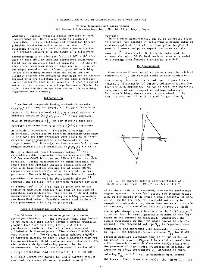
ELECTRICAL SWITCHING IN CADMIUM BORACITE SINGLE CRYSTALS
Tatsuo Takahashi and Osamu YamadaRCA Research Laboratories, Inc., Machida City, Tokyo, Japan
Abstract - Cadmium boracite single crystals at hightemperatures ( 300DC) were found to exhibit areversible electric field-induced transition betweena highly insulative and a conductive state. Theswitching threshold is smaller than a few volts foran electrode spacing of a few tenth of a millimeter
? 3corresponding to an electric field of 10" 10 V/cm.This is much smaller than the dielectric break-downfield for an insulator such ds boracite. The insula-tive state reappears after voltage removal. A pulsetechnique revealed two different types of swi tching.Unstable switching occurs when the pulse voltages1i ghtly exceeds the switching threshold and is charac-terized by a pre-switching delay and also a residua]current after voltage pulse removal. A stable type ofswitching occurs when the voltage becomes sufficientlyhigh. Possible device applications of this switch ingphenomenon are discussed.
Introduct ion
recorder.In the pulse measurements, the pulse generator (Toyo
Telesonics) was capable of delivering a square pulse ofmaximum amplitude 10 V with various pulse lengths (1(jsec 10 msec) and pulse repetition rates (single
sweep "M0 pulses/sec). Both the dc pulse and thecurrent through a 50 Kft load resistance were recordedon a storage osci1loscope (Tektronix type 564).
DC Measurement
When <i crystal was heated to above a certain criticaltemperature T , the crystal could be made conductive
cupon the applicat ion of a dc voltage. Figure l i s aschematic illustration of current-voltage characteris-tics for such switching. As can be seen, the switchingi s symmotrical with respect to voltage polarity.Be fore swi telling, the current is determined by thesample resistance since it is much larger than R .
A series of compounds having a chemical formulaM B O X (M = divalent metal, X = ha]ogen) have been
known to be isostructural with the mineral magnesiumchlorine boracite (Mg B 0 Cl). 3 These compounds
have an orthorhombic C^ -Pea structure at room tem-2v 5 -
peraturc and transform to a cubic T -F43c structure
at a higher temperature. Extensive investigationsof physical properties of boracite compounds were madein the past and some boracites were found to be ferro-electric and ferromagnetic simultaneously at lowtemperatures. Recently, we have successfully grownsingle crystals of Cd boracites, Cd,B7O13X; X = Cl or
Br, by a chemical vapor transport method. Thecrystallographic transition temperatures were 520 +5°C for the Cd-Cl boracite and 430 + 5°C for the Cd"-Brboracite. During measurements on these crystals, wefound that the crystals abruptly became conductivewhen a dc bias voltage was applied at above 300°C,temperatures considerably below the transition tem-perature. The switching was reproducible and closely
resembled that observed in chalcogenide glasses.However, the critical field strength required for such
switching (10 ^ 10 V/cm) was at least one or twoorders of magnitude smaller than that in the case ofamorphous semiconductors. The results of dc and pulsemeasurements of this interesting switching phenomenonare described below. Possible device applications ofthis phenomenon will also be discussed.
Sample Preparation and Measuring Technique
The Cd boracite crystals were grown by a methoddescribed elsewhere.*•" The crystals (max. edge lengthV> mm) were cut into slices having a simple crystallo-graphic face such as (100), (110), and (111) inpseudo-cubic indices. Each slice was ground andpolished with diamond paste. Electrodes of Au/Cr filmwere evaporated. The Cr inner layer adheres rigidlyto boracite surface to make a good supporting film forthe Au overlayer. Gold lead wires were attached to theelectrodes with Ag-conducting paste. In the dcmeasurements, the sample was connected in series with
a large protective load resistance (L (10 100 KT2).
A voltage across the sample (X) and a current throughthe load resistance (Y) were recorded on an X-Y
Fig. 1. dc current-voltage characteristics of aCd-X boracite crystal (X = Cl or Br) at T > T .
After the threshold is exceeded, a negative resistanceregion appears. In the 'on' state, the dynamic resist-ance of the sample dV/dl takes a small positive or zerovalue. Unlike the case of threshold switching inamorphous semiconductors, there does not exist a criti-cal current, or a so-called holding current at which
the sample abruptly switches back to the 'off state.It seems that the sample gradually returns to the 'offstate as the current is decreased. Therefore, thesample resistance in the 'on' state cannot be clearlydefined. Tht threshold voltage V is dependent upon
temperature and decreases with temperature increase.In Fig. 2, the temperature variation of V , for Cd-Cl
th
boracite sandwich electrode samples of two differentthickness are shown. Figure 3 is a similar result fora Cd-Br boracite sandwich electrode sample that showsthe presence of temperature hysteresis on cooling. Anapparent critical temperature T , obtained by extra-polating Vth to infinity, is dependent upon samplethickness. The thicker the sample, the higher T . The
67
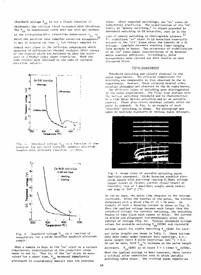
threshold voltage V is nota linear function of
thickness; the crit ical field increases with thickness.The V vs temperature curve does not show any anomaly
at the crystallographic transition temperature T attr 10
which the peculiar twin lamellar struct ure disappears.It may be pointed out that T lor thinner samples is
indeed very close Co the inflexion temperature whichappeared in differentia1 thermal analysis (OTA) curvesof che crystal which are believed to show the exist-ence of a hip.her order phase transi t ion, Much thesame results were obtained in the case of coplanareiuf t rode .sampH-s.
value. After repeated switchings, the 'on' state istemporarily stabilized. The stabilization of the 'on'state, or 'memory switching,' is always preceded bythreshold switching in Cd boracites, just as in the
case of memory switching in chalcogenide glasses.Ii.i- stabilized 'on1 state in Cd boracites eventuallyreturns to the 'off' state after the removal of a dcvo) tage. Complete recovery requires times rangingfrom seconds to hours. The occurrence of stabilizationof an 'on* state makes interpretation of dc measure-ments somewhat ambiguous. Accordingly, pulsemeasurements were carried out with results as nextd i scussed below.
Pulse Experiments
Cd-CiB (OOi)Cut
(Heating)
V r-200 300 AQQ
Temperature (*C)500
Fig. - . ThrcsiioUl volt;in<-' V >1!i a function of tem-perature for two Cd-C'l horncitu sandwich electrodesamples with different lOectrodu : , r . - i n s s .
Cd-BrB {00 I) Cu»O 38 mm trsck
" Healing
"• Cooling
L J200 300 400 500
Terrperature CC)
Fig. 3. Threshold voltage V as a function oftemperature for a Cd-Br boracite sandwich electrodesample.
When a sample is kept in the 'on' state at a certaintemperature, stabilization of the conductive stateseems to set in. That is, if the 'on' state is main-tained for a short time, V measured immediately
thafterwards is considerably smaller than its previous
Threshold switclung was clearly observed in thepulse experiments. The critical temperature forswitching was comparable to that observed in the dcexperiments. However, there occurred several otherpeL'u] iar phenomena not observed in the dc experiments.Two different types of switching were distinguished
in the pulse experiments. The first type appears nearthe voltagf swi tching threshold and is characterizedby a t ime delay before switching and by an unstablecurrent. There also exists residual current after thepulse is removed. In Fig. 4, an example of such'unstable* switching is shown. The photograph wastaken by multiple exposures at various pulse voltages.
Fig. h. Scope trace of unstable switching pulse(multiple exposure). Cd-Br boracite sandwich elec-trode sample with electrode spacing 0,38mm; voltage(upper trace) of 2V/div; current (lower trace) of40uA/div; time of 2 msec/div; single sweep trace;and temp of 340° + 2°C.
As can be seen, the delay time shortens as the voltageincreases. After the removal of the pulse, the currentdisappears with a decay time of 15 20 ysec. Anexample of such a decaying current is shown in Fig. 5.When the applied voltage becomes much larger than thethreshold voltage for unstable switching, the switchingbegins to take place with almost no delay. The currentis stable and disappears instantaneously after the:removal of voltage (Fig. 6). Typical threshold voltagevalues for unstable switching V (USSW) and threshold
voltage values for stable switching V (SSW) for vari-tn
ous Dulse lengths are shown in Table I. These voltagedata were taken under constant duty operation, i.e.,pulse length (sec) X pulse repetition (sec ) =0.1.As can be seen, both V *s increase as the pulse lengthdecreases. V (SSW) is at least
th times V L(USSW).thWhen the applied voltage is kept constant, there existsa critical pulse repetition rate at which unstableswitching takes place. The critical pulse repetition
68
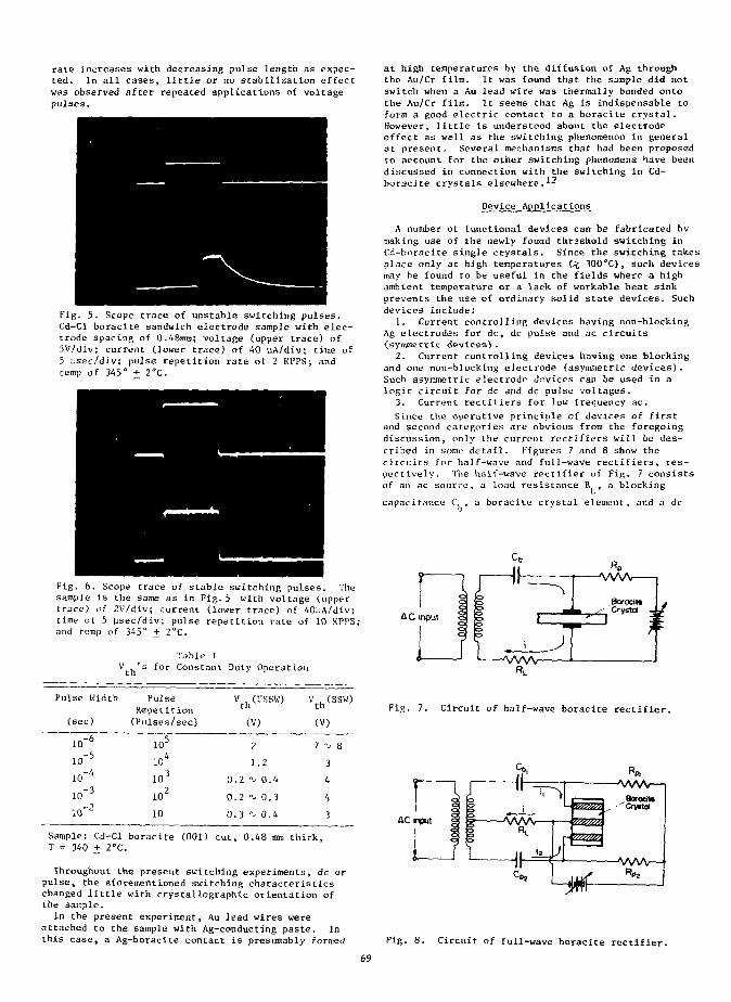
rate increases with decreasing pulse length as expec-ted. In all cases, little or no stabilization effectwas observed alter repeated applications of voltagepulses.
Fig. 5. Scope trace of unstable switching pulses.Cd-Cl boracite sandwich electrode sample with elec-trode spacing of 0.48mm; voltage (upper trace) of5V/div; current (lower trace) of 40 uA/div; time of5 (jsec/div; pulse repetition rate of 2 K.PPS; andtemp of 345° + 2°C.
Fig. 6. Scope trace of stable switching pulses. Thesample is the same as in Fig.5 with voltage (uppertrace) of 2V/div; current (lover trace) of 40pA/div;time of 5 usec/div; pulse repetition rate of 10 KPPS;and temp of 345° + 2°C.
Table IV 's for Constant Duty Operation
Pulse Width
(sec)
10'6
w'b
io"A
1O"3
10 ~
PulseRepetition(Pulses/sec)
10S
10*
10 3
io2
10
0
0
0
veh<ussw)
(V)
2
1.2
.2 % 0.4
.2 -v. 0.3
.3 ^ 0.4
vth(ssw)
(V)
7^8
3
4
4
3
Sample: Cd-Cl boracite (001) cut, 0.48 mm thick,T = 340 + 2°C.
Throughout the present switching experiments, dc orpulse, the aforementioned switching characteristicschanged little with crystallographic orientation ofthe sample.In the present experiment, Au lead wires were
attached to the sample with Ag-conducting paste. Inthis case, a Ag-boracite contact is presumably formed
at high temperatures by the diffusion of Ag throughthe Au/Cr film. It was found that the sample did notswitch when a Au lead wire was thermally bonded ontothe Au/Cr film. It seems chat Ag is indispensable toform a good electric contact to a boracite crystal.However, little is understood about the electrodeeffect as well as the switching phenomenon in generalat present. Several mechanisms that had been proposedto account for the other switching phenomena have beendiscussed in connection with the switching in Cd-boracite crystals elsewhere.^
Device Applications
A number of functional devices can be fabricated bymaking use of the newly found threshold switching inCd-boracite single crystals. Since the switching takesplace only at high temperatures Ci 300°C), such devicesmay be found to be useful in the fields where a highambient temperature or a lack of workable heat sinkprevents the use of ordinary solid state devices. Suchdevices include:
1. Current controlling devices having non-blockingAg electrodes for dc, dc pulse and ac circuits(symmetric devices).
2. Current controlling devices having one blockingand one non-blocking electrode (asymmetric devices).Such asymmetric electrode devices can be used in alogic circuit for dc and dc pulse voltages.
3. Current rectifiers for low frequency ac.
Since the operative principle of devices of firstand second categories are obvious from the foregoingdiscussion, only the current rectifiers will be des-cribed in some detail. Figures 7 and 8 show thecircuits for half-wave and full-wave rectifiers, res-pectively. The half-wave rectifier of Fig. 7 consistsof an ac source, a load resistance IL , a blocking
capacitance C , a boracite crystal element, and a dcb
A C inpul
Fig. 7. Circuit of half-wave boracite rectifier.
AC input
Fig. 8. Circuit of full-wave boracite rectifier.
69
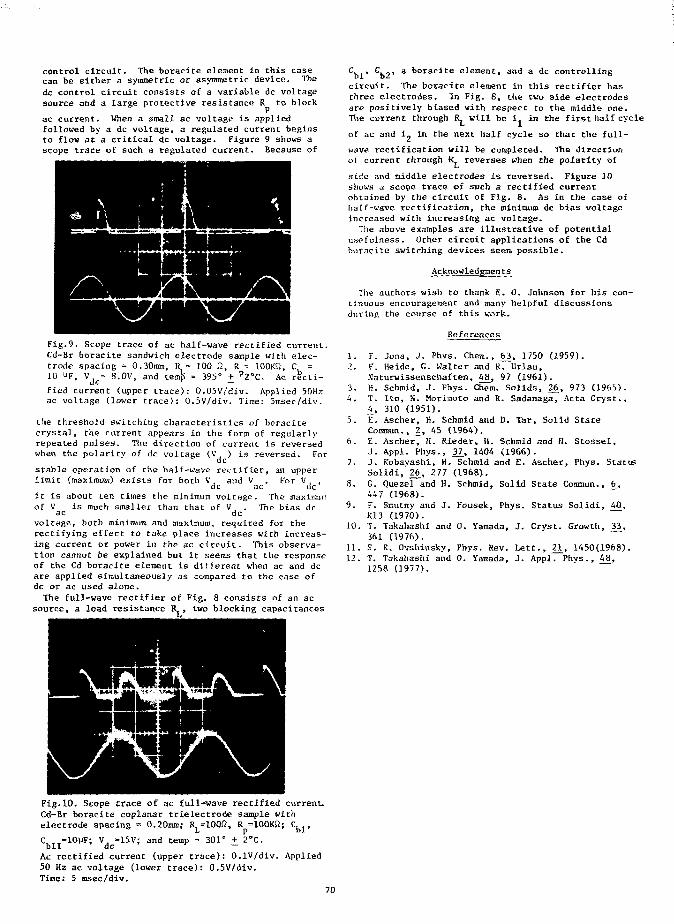
control circuit. The boracite element in this casecan be either a symmetric or asymmetric device. Thedc control circuit consists of a variable dc voltagesource and a large protective resistance R to block
ac current. When a small ac voltage is appliedfollowed by a dc voltage, a regulated current beginsto flow at a critical dc voltage. Figure 9 shows ascope trace of such a regulated current. Because of
Fig.9. Scope trace of ac half-wave rectified current.Cd-Br boracite sandwich electrode sample with elec-trode spacing = 0.30mm, R = 100 Q, R = 100KB, C =10 Vf, VJc= 8.0V, and temp = 395° +
P2"C. Ac recti-fied current (upper trace): 0.05V/div. Applied 50Hzac voltage (lower trace): 0.5V/div. Time: 5msec/div.
the threshold switching characteristics of boracitecrystal, the current appears in the form of regularlyrepeated pulses. The direction of current is reversedwhen the polarity of dc voltage (V ) is reversed. For
dcstable operation of the half-wave rectifier, an upper
For Vlimit (maximum) exists for both V and Vdc ac dc'
it is about ten times the minimum voltage. The maximumof V is much smaller than that of V . The bias dc
ac dcvoltage, both minimum and maximum, required for therectifying effect to take place increases with increas-ing current or power in the ac circuit. This observa-tion cannot be explained but it seems that the responseof the Cd boracite element is different when ac and dcare applied simultaneously as compared to the case ofdc or ac used alone.The full-wave rectifier of Fig. 8 consists of an ac
source, a load resistance 1L , two blocking capacitances
Fig.10. Scope trace of ac full-wave rectified current.Cd-Br boracite coplanar trielectrode sample withelectrode spacing = 0.20mm; R=100ft, R =100Kfl; Cfa ,
C,. =10UF; V. =15V; and temp = 301° + 2°C.bll dc ~*
Ac rectified current (upper trace): O.lV/div. Applied50 Hz ac voltage (lower trace): 0.5V/div.Time: 5 rasec/div.
C , cb2»
a koracite element, and a dc controlling
circuit. The boracite element in this rectifier hasthree electrodes. In Fig. 8, the two side electrodesara positively biased with respect to the middle one.The current through 1^ will be 1, in the first half cycl
of ac and i, in the next half cycle so that the full-
wave rectification will be completed. The direction
of current through R reverses when the polarity of
side and middle electrodes is reversed. Figure 10shows a scope trace of such a rectified currentobtained by the circuit of Fig. 8. As in the case ofhalf-wave rectification, the minimum dc bias voltageincreased with increasing ac voltage.The above examples are illustrative of potential
usefulness. Other circuit applications of the Cdboracite switching devices seem possible.
Acknowledgmen ts
The authors wish to thank E. 0. Johnson for his con-tinuous encouragement and many helpful discussionsduring the course of this work.
References
1. F. Jona, J. Phys. Chem., 6J}, 1750 (1959).2. F. Heide, G. Walter and R. Urlau,
Naturwissenschaften, 48, 9? (1961).3. H. Schmid, J. Phys. Chem. Solids, 26 , 973 (1965).i. T. Ito, N. Moriraoto and R. Sadanaga, Acta Cryst.,
4_, 310 (1951).5. E. Ascher, H. Schmid and D. Tar, Solid State
Commun., 2, 45 (1964).6. E. Ascher, H. Rieder, H. Schmid and H. Stossel,
J. Appl. Phys., 37_» 1 4 0 4 (1966).7. J. Kobayashi, H. Schmid and E. Ascher, Phys. Status
Solidi, 26, 277 (1968).8. G. Quezel and H. Schmid, Solid State Commun., 6,
44 7 (1968).9. F. Smutny and J. Fousek, Phys. Status Solidx, 40,
K13 (1970).10. T. Takahashi and 0. Yamada, J. Cryst. Growth, yi,
361 (1976).11. S. R. Ovshinsky, Phys. Rev. Lett., 21, 1450(1968).12. T. Takahashi and 0. Yaroada, J. Appl. Phys., 4J3,
1258 (1977).
70
fWHATEVER HAPPENED TO SILICON CARBIDE
R. B. CampbellWestinghouse Electric Corporation
P. O. Box 10864Pittsburgh, PA 15236
Summary
Silicon carbide has been used extensively as anabrasive, but only in the last twenty-five years hasits potential as a semiconductor been exploited. Therationale for SiC semicondu*. tor devices is their hightemperature nerformance. Rectifiers, field effecttransistors, charged particle detectors, and otherdevices operate efficiently at temperatures about800°K.
It is the purpose of this paper to examine theprogress made in SiC devices in the 1955-1975 timeframe am" suggest reasons for the present lack orinterest ir this unique material. The data given inthis paper has bocn abstracted from previous] >' pub-lished work.
Introduct ion
In the last seventy years, considerable use hasbeen made of the abrasive characteristics of siliconcarbide (hereafter SiC): however, only recently were
(1-4)its potentialities as a semiconductor exploited.It is the purpose of this paper to discuss SiC devicesin the 1955-1975 time frame. Since SiC device proper-ties are intimately connected with its material proper-ties, crvstal growth and fabrication techniques willalso be discussed. Finally, I will suggest reasons itIs no longer considered a viable product for exploita-tion.
The work discussed in this paper was performed atvarious industrial and college research laboratories.These programs are no longer active, and there are noknown plans or interest in their reactivation.
Physical and Chemical Properties
Silicon carbide exists in the hexagonal (a) andcubic (B) phases with the a phase occurring in a vari-ety of polytypes. The various forms of SiC have thelargest energy gaps found in common semiconductormaterials, ranging from 2.39 eV (cubic) to 3.33 eV (2H).The bonding of Si and C atoms is basically covalentwith about 12% ionic bonding. The structures are tem-perature stable below 1800°C and thus form a family ofsemiconductors useful for high temperature electronicdevices. Table 1 shows the lattice parameters andenergy gap (0°K) for the common polytypes.
Table 1. Lattice Constants and Energy Cap of Common SIC Polytypes
Structure
2H
4H
6H
33R
15R
21R
8H
cublc-3c
a
a
a
a
a
•
Lattice
- 3.09
- 3.09
- 3.0817
• 3.079
- 3.079
>» « . 3 5 9
Parameters
(X), c "
i c •
, c •
, c •
, c •
5.048
10.05
15.1183
37.78
52.88
Energy Gap
3.33
3.26
3.02
3.01
2.986
2.86
2.80 - 2
2.39
(0°K)
.90
SiC is inert to nearly all laboratory reagents,and the usual techniques for chemical etching employmolten salt or salt mixtures (NaOH, Ma?0» borax) at
temperatures above 600°C, Electrolytic etching, suita-ble for p-type material and etching with gaseous chlo-rine near 1000°C, may also be used.
The physical hardness and chemical inertness im-pose great restraints on device fabrication techniques.Although SiC technology lias progressed along the same1ines as that of si.I icon, many techniques had to bedeveloped which were pecul far to SiC. and which inevi-tably made the fabrication more difficult and expen-sive.
Methods of Preparntion
The oldest and perhaps the best known method ofSIC crvstal growth is the subl itnat ion method. Thistechnique uses the vaporization of a SiC charge atabout 23OO°C into a cooler cavity with subsequent con-densation. Initially the charge formed its own cavitv,but more uniform crystals are grown wfien a thin graph-ite cylinder is used in the center of the charge. Thisthin cylinder also reduces the number of nucleations sothat fewer but more perfect crystals are grown. Thecrystals are grown as thin hexagona, platelets, perpen-dicular to the growth cavity. Doped crystals, contain-ing p-n junctions, can be prepared by adding properdopants to the ambient during growth. The power rect i-fiers, to be described later, were prepared by thismethod.
Other methods of crystal growth are epitaxy, trav-eling solvent and solution growth.
The fiexagonal a phase is grown epitaxially from1725° to 1775 C with the cubic phase being grown from1660°C to 1700°C. In both cases, equal molar percent-ages of CC1. and SiCl, are used. Polished and etched
h ASiC crystals were generally used as substrates althoughRyan and co-workers at Air Force Cambridge ResearchLaboratorv have investigated the growth of SiC ontocarbon substrates using the hydrogen reduction ofmethyltrichlorosilane (CH-SiCl ) (called the vapor-liquid-solid growth). At 1500°C, a-SiC whiskers on theorder of 5 mm long by 1 mm diameter were grown. Thesewhiskers were of the relatively rate 2H polytype.
SiC crystals have been grown together, and p-njunctions formed by passing a heat zone through two SiCcrystals separated bv a solvent metal (traveling sol-vent). The temperature gradient across the thin sol-vent zone causes dissolution at both solvent-solidinterfaces. However, the equilibrium solubility of SiCin the solvent is greater at the hotter interface, aconcentration gradient: is established. The solute,then, will diffuse across the liquid zone and precipi-tate onto the cooler crystal. In this way, two dissimt-lar conductivity type SiC crystals can be grown togeth-er.
In the solution growth technique, a small amountof SiC is dissolved in molten Si (or in some cases Feor Cr). As the melt is slowly cooled, the SiC becomesless soluble; and SiC crystals nucleate and grow in thecrucible on prepared graphite substrates. The growncrystals are normally of the 6-phase. Improvements inthe crucible geometry and cooling rates have led to
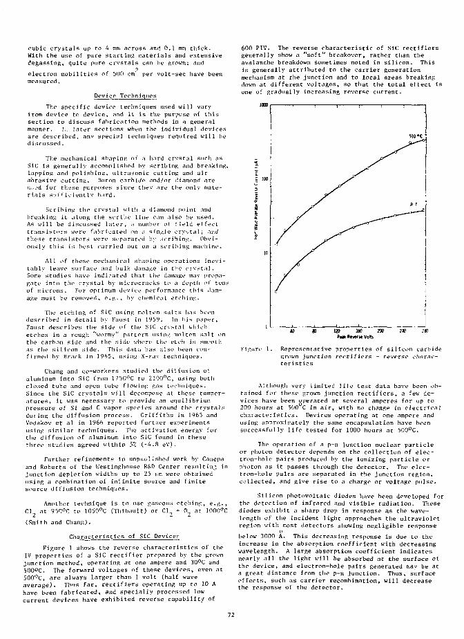
cubic crystals up to A mm across and 0.1 mm thick.With the use of pure starting materials and extensivedegassing, quite pure crystals can he grown; and
2electron mobilities of 500 cmmeasured.
per volt-sec have been
Device Techniques
The specific device techniques used will varyfrom device to device, and it is the purpose of thissection to discuss fabrication methods in a generalmanner. I,, later sections when the individual devicesare described, any special techniques required wil1 bediscussed.
The mechanical shaping of a hard crvstal sucli asSiC is generally accomplished by scribing and breaking,lapping and polishing, ultrasonic cutt ing and ai rabrasive cutting. Boron carbide and/or diamond areu.-.'d for these purposes since they are the only mate-rials sufficiently hard.
Scr ib ing the crystal with a diamond point andbreaking it along the scribe line can also be used.As will be d iscussed later, n number of field effecttrans istors were fabricated on a s ingIe crystal; nndthese transistors were separated by scribing. Obvi-ously this is bust carried nut on a scribing machine.
All of these mechanical shaping operations inevi-tably leave surface and bulk damage in the crystal.Some studies have ind icated that the damage may propa-gate into tfie crystal by mlc roc racks to a depth of tensof microns. For opt imum dev ice performance this dam-age must be removed, e.g., by chemical etelling.
The etching of SiC using molten salts lias beendescribed in detail by Faust in 1959. Tn his paper,Faust describes the side of the SiC crvstal whichetches in a rough "wormy" pattern using molten salt onthe carbon side and the side where the etch is smoothas the s i 1 icon H ide . This data lias al so been con-f i rmed bv Brack in 1965, usi n^ X-r-ny techniques.
Chang and co-workers studaluminum into SiC from 175O°Cclosed tube and open tube flowSince the SiC crystals will deatures, it was necessary to prpressure of Si and C vapor spedur ing the diffusion process.Vodakov et al in 1966 reportedus ing similar techniques. Thethe diffusion of aluminum intothree studies agreed within 5%
ied the diffus ion ofto 2100°C, using bothing gas techniques.compose at these temper-ovide an equilibriumcies around the crystalsGriffiths in 1965 andfurther experimentsactivation energy forSiC found in these(-4.8 eV).
Further refinements in unpublished work by Canepaand Roberts of the Westinghouse R&D Center result in3 injunction depletion widths up to 25 urn were obtainedusing a combination of infinite source and finitesource di ffus ion techniques.
Another technique is to use gaseous etching, e.g.,Cl at 950°C to 1050°C (Thibauit) or Cl2 + C>2 at IO00°C
(Smith and Chang).
Characteristics of SiC Devicer
Figure 1 shows the reverse characteristics of theIV properties of a SiC rectifier prepared by the grownjunction method, operating at one ampere and 30°C and500°C. The forward voltages of these devices, even at500°C, are always larger than 1 volt (half waveaverage). Thus far, rectifiers operating up to 10 Ahave been fabricated, and specially processed lowcurrent devices have exhibited reverse capability of
600 PIV. The reverse characteristic of SiC rectifiersgenerally show a "soft" breakover, rather than theavalanche breakdown sometimes noted in silicon. Thisis generally attributed to the carrier generationmechanism at the junction and to local areas breakingdown at different voltages, so that the total effect isone of gradually increasing reverse current.
170 J60 200Peak Reverse Volts
Figure 1. Representative properties of silicon carbidegrown junction recti fiers - reverse charac-teristics
Although very Iimited 1i fe test data have been ob-t<iined for these grown junction rectifiers, a few de-vices have been operated at several amperes for up to200 hours at 500 C in air, with no change in electricalcharacteristics. Devices operating at one ampere andusing approximately the same encapsulation have beensuccessfully life tested for 1000 hours at 500°C.
The operation of a p-n junction nuclear particleor photon detector depends on the collection of elec-tron-hole pairs produced by the ionizing particle orphoton as it passes through the detector. The elec-tron-hole pairs are separated in the junction region,collected, and give rise to a charge or voltage pulse.
Silicon photovoltaic diodes have been developed forthe detection of infrared and visible radiation. Thesediodes exhibit a sharp drop in response as the wave-length of the incident light approaches Che ultravioletregion witli most detectors showing negligible response
obelow 3000 A. This decreasing response is due to theincrease in the absorption coefficient with decreasingwavelength. A large absorption coefficient indicatesnearly all the light will be absorbed at the surface ofthe device, and electron-hole pairs generated may be ata great distance from the p-n junction. Thus, surfaceeffects, such as carrier recombination, will decreasethe response of the detector.
72
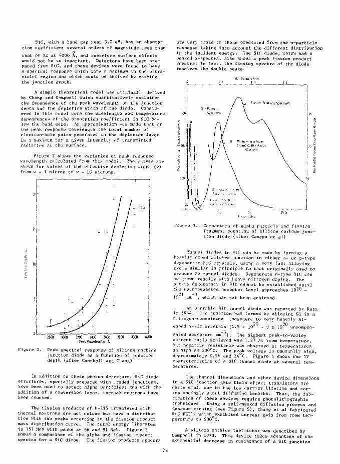
SiC, with a band gap near 3.0 eV, has an absorp-tion coefficient several orders of magnitude less than
othat of Si at 4000 A, and therefore surface effectswould not be so important. Detectors have been pre-pared from SiC, and these devices were found to havea spectral response which were a maximum in the ultra-violet region and which could be shifted by varyingthe junction depth.
A simple theoretical model was originall< derivedby Chang and Cimpbell which quantitatively explainedthe dependence of the peak wavelength on the junctiondepth and the depletion width of the diode. Consid-ered in this model were the wavelength and temperaturedependences of the absorption coefficient in SiC be-low the band edge. An approximation was made that atthe peak response wavelength the total number ofelectron-hole pairs generated in the depletion layeris a maximum for a given intensity of transmittedradiation ct the surface.
Figure 2 shows the variation of peak responsewavelength calculated from this model. The curves areshewn for values of the effective depletion width (w)from w = 1 micron to w = 10 microns.
2800 3000 3200 MOO 3(00Peak Wavelength. J,
3800 3000
Figure Peak spectral response of si.licon carbidejunction diods as a function of junctiondepth (after Campbell and C ang)
In addition to these photon detectors, SiC diodestructures, specially prepared with : raded junctions,have been used to detect alpha particles; and with theaddition of a conversion layer, thermal neutrons havebeen counted.
The fission products of U-235 irradiated withthermal neutrons are not unique but have a distribu-tion with two peaks occurring in the fission productmass distribution curve. The total energy liberatedis 157 MeV with peaks at 66 and 91 MeV. Figure 3shows a comparison of the alpha and fission productspectra for a SiC diode. The fission products spectra
are very close to those predicted from the a-particleresponse taking into account the different distributionin the incident energy. The SiC diode, which had apeaked a-spectra, also shows a peak fission productsoectra; in fact, the fission spectra of the dioderesolves the double peaks.
'Ki.t-n •.!„
Figure 3. Comparison of alpha particle and fissionfragment counting of silicon carbide junc-tion diode (after Canepa et al)
Tunnel diodes in SiC can be made by forming aheavily doped alloyed junction in either n- or p-typedegenerate SiC crystals, using a very fast alloyingcycle similar in principle to that originally used toproduce Ge tunnel diodes. Degenerate n-type SiC canhe grown readily with heavy nitrogen doping. Thep-tvpe degeneracy in SiC cannot be established untilthe uncompensated acceptor level approaches
10'21 -3
which has not been achieved.
An operable SiC tunnel diode was reported by Rutzin 1964. The junction was formed by alloying Si in anitrogen-containing tmosphere to very heavily Al-
doped a-SiC crystals (4.5 x 10 2 0 - 9 x KT° uncompen-sated acceptors cm ). The highest peak-to-valleycurrent ratio achieved was 1.37 at room temperature,but negative resistance was observed at temperaturesas high as 500°C. The peak voltage is unusually high,approximately 0.9V and 24 C. Figure 4 shows the IVcharacteristics of a SiC tunnel diode at several tem-peratures .
The channel dimensions and other device dimensionsin a SiC junction gate field effect transistors arequite small due to the low carrier lifetime and cor-respondingly short diffusion lengths. Thus, the fab-rication of these devices require photolithographictechniques. Using a self-masked diffusion process andgaseous etching (see Figure 5), Chang et al fabricatedSic FET's which exhibited current gain from room tem-perature to 500 C.
A silicon carbide thermistor was described byCampbell in 1973. This device takes advantage of theexponential decrease in resistance of a SiC junction
73
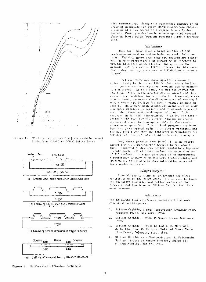
Figure '•> • IV charm: t er ist Irs of silicon rarbidv tunnt-1diodf from - l W T to 400°C (after Rut7.)
Carbon-Face SiCL Mask
/ — -
n-fype
Diffused p-
\
SiC
type
--
SiC
la) Section view, oxide mask after photoresist etch
<b) Following Cl - 0 , etch and removal of oxide
p-type
Ic) Following second diffusion of p-type impurity
Source
r1Gate
Gate
DrainGale
Gate
Source
Idf "Self-mask" removed leaving finished structure
Figure 5. Self-maskPcI diffusion technique
with temperature. Since this resistance changes by anorder of magnitude for every 1OO°C temperature change,a change of a few tenths of a degree is easily de-tected. Prototype devices have been operated severalthousand hours (wi th frequent rye H n g ) without degrada-1 i nn -
Conclusions
Thus f.ir I have t;iven a brief out 1 ine of SiCsemiconductor devices and methods for their fabrica-t ion. T!ie data given show that SiC devices are feasi-b le and have propert ies that should be of interest toseveral h i 'n technology fields. The question thenarisL-s: l-.'hv is there so little interest in this mate-r i al todayi and why are there no SiC devices currentlyin use?
I helieve there are throe riper i fie reasons forthis. Fi rst, in the later 1960's there was u dec]inein corporate and C'ove rntnent R&D fund i nc, due to econom-ic conditions. At this time, SiC had not carved outi t s niche1 in the st- mi conduct nr device market and thuswas a prime cand idate for anv cutback. A second, sone-ivbat re 1 a ted, cause was the disappearance of the snal 1m.irket where SiC devices did have a chance to make animpact. Tin1 so were hiu.ii techno] oj;y areas such as nearsun spice miss ions, supersonic and hvpersonic aircraft,etc . When these markets di sapper red» much of theinterest in SiC nlsc <iisap;>t:-,irt'd. Finallv, the fabri-c.it ion techn iqut's for SiC dev ices ( induiii nj; growthmethods) did not improve apprec iablv in the t'*vntvvears under quest ion. This lack of progress r:ny iiavebeen due to misplaced onphasis in devi ce prourams, butthe net result was that the fabrication techniques forSiC devices improved onlv slij'hrlv fn this tirr.e span.
N'ow, where do wo go from iiere'.1 J see no viabl emarket for SiC semi conductor devi ct? s in the near fu-ture. Improved Si devices, bet ter insulation, improvedc i rcui t design all mi t i ate against anv extensive useof SiC devices. This nav be viewed as an unfortunatecircumstance to many of us who were professional 1 -• andemotionallv involved with this interesting materialfor a number of vears.
Ackn oyjy dgmunts
1 would I ike to thank my col leagues for theircontributions to the ziven data. I a3 so wish to thankthe Executive Committee and fellow members of theInternational Committee on Silicon Carln'cie for theirencouragement.
R eferences
Tht' fo11 owing four references contain a11 the workdiscussed in this paper.
1. Silicon Carbide, A High Temperature Semiconductor,Perpamon Press, New York, 1960.
2. Silicon Carbide - 1968; Pergamon Press, New York,1969.
3. Silicon Carbide - 1973; Edited R. C. Marshall,J. W. Faust and C. E. Ryan, Univ. of South Caro-lina Press, Columbia, S.C., 1974.
k. Silicon Carbide as a Semiconductor; J. FeitknechtSpringer Truets in Modern Physics, Volume 58;Springer-Verlay, Berlin, 1971.
74
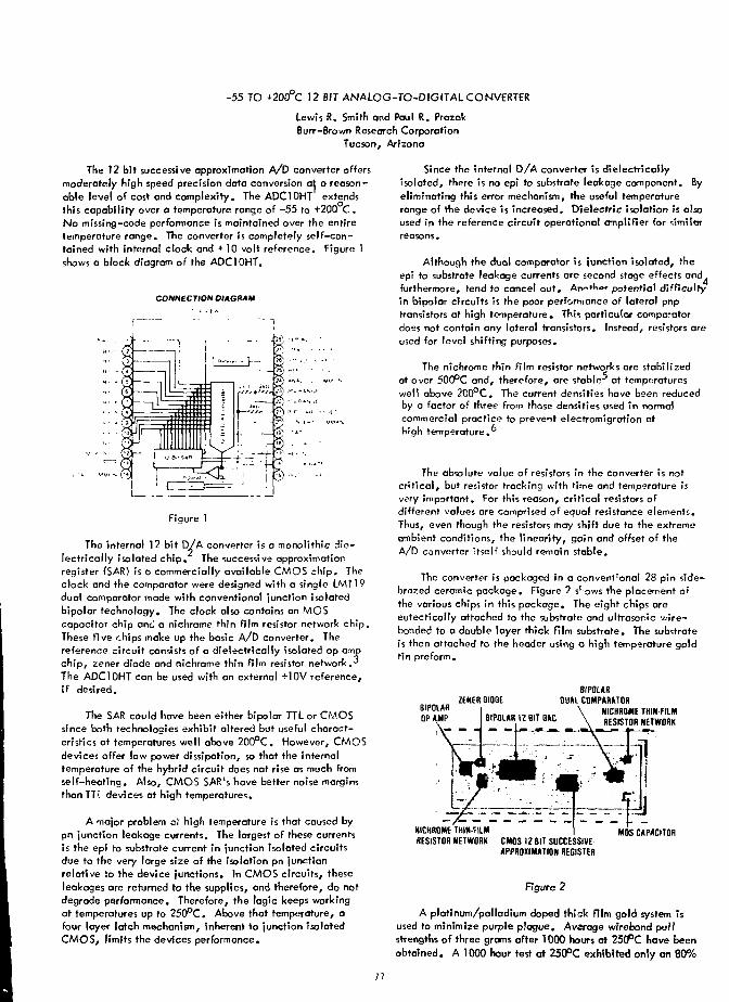
-55 TO +200 C 12 BIT ANALOG-TO-DIGITAL CONVERTER
Lewis R. Smith and Paul R. PrazokBun—Brown Research Corporation
Tucson, Arizona
The 12 bit successive approximation A/D converter offersmoderately high speed precision data conversion at a reason-able level of cost and complexity. The ADCIOHT extendsthis capability over a temperature range of -55 to +200 C.No missing-code performance is maintained over the entiretemperature range. The converter is completely self-con-tained with internal clock and +10 volt reference. Figure 1shows a block diagram of the ADCIOHT.
CONNECTION DIAGRAM
Figure 1
The internal 12 bit D/A converter is a monolithic die-lectrically isolated chip. The successive approximationregister (SAR) is a commercially available CMOS chip. Theclock and the comparator were designed with a single LMl 19dual comparator made with conventional junction isolatedbipolar technology. The clock also contains an MOScapacitor chip anc a nichrome thin film resistor network chip.These five chips make up the basic A/D converter. Thereference circuit consists of a dielectrically isolated op ompchip, zener diode and nichrome thin film resistor network.3The ADCIOHT can be used with an external +10V reference,if desired.
The SAR could have been either bipolar TTL or CMOSsince both technologies exhibit altered but useful charact-eristics at temperatures well above 200°C. However, CMOSdevices offer low power dissipation, so that the internaltemperature of the hybrid circuit does not rise as much fromself-heating. Also, CMOS SAR's have better noise marginsthanTTi devices at high temperatures.
A major problem at high temperature is that caused bypn junction leakage currents. The largest of these currentsis the epi to substrate current in junction isolated circuitsdue to the very large size of the isolation pn junctionrelative to the device junctions. In CMOS circuits, theseleakages are returned to the supplies, and therefore, do notdegrade performance. Therefore, the logic keeps workingat temperatures up to 250°C. Above that temperature, afour layer latch mechanism, inherent to junction IsolatedCMOS, limits the devices performance.
Since the internal D/A converter is dielectricallyisolated, there is no epi to substrate leakage component. Byeliminating this error mechanism, the useful temperaturerange of the device Is increased. Dielectric isolation is alsoused in the reference circuit operational amplifier for similarreasons.
Although the dual comparator is junction isolated, theepi to substrate leakage currents are second stoge effects andfurthermore, tend to cancel out. Arv^^o*- potential difficultyin bipolar circuits Is the poor performance of lateral pnptransistors at high temperature. This particular comparatordoes not contain any lateral transistors. Instead, resistors areused for level shifting purposes.
The nichrome thin film resistor networks are stabilizedat over 500°C and, therefore, ore stable"1 at temperatureswell above 200°C. The current densities have been reducedby a factor of three from those densities used in normalcommercial practice to prevent electromigration athigh temperature.°
The absolute value of resistors in the converter is notcritical, but resistor tracking with time and temperature isvery important. For this reason, critical resistors ofdifferent values are comprised of equal resistance elements.Thus, even though the resistors may shift due to the extremeambient conditions, the linearity, gain and offset of theA/D converter itself should remain stable.
The converter is packaged in a conventional 28 pin side-brazed ceramic package. Figure 2 s' ows the placement ofthe various chips in this package. The eight chips areeutectically attached to the substrate and ultrasonic wire-bonded to a double layer thick film substrate. The substrateis then attached to the header using a high temperature goldtin preform .
BIPOLAROP AMP
ZtHES QlOOtBIPOLAR
DUAL COMPARATORNICHROME THIN-FILMRESISTOR NETWORK
NICHROME THIN-FILMRESISTOR NETWORK CMOS 12 RIT SUCCESSIVE
APPROXIMATION REGISTER
MOS CAPACITOR
Figure 2
A platinum/palladium doped thick film gold system isused to minimize purple plague. Avaroge wfrebond puflstrengths of three grams after 1000 hours at 250°C have beenobtained. A 1000 hour test at 250°C exhibited only an 80%
77
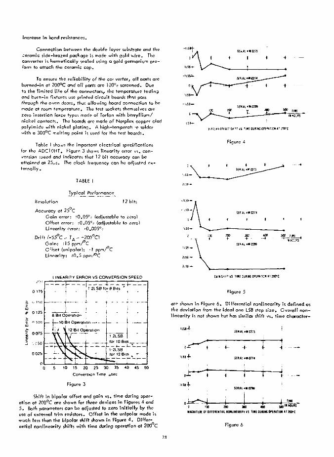
increase in bond resistances.
Connection between the double layer substrate and theceramic side-brazed packoge is made with gold wire. Theconverter is hermetically sealed using a gold germanium pre-form to attach the ceramic cap.
To ensure the reliability of the converter, all parts areburned-in at 200°C and all parts are I00°c screened. Dueto the limited life of the connectors, the temperature testingand burn-in fixtures use printed circuit boards thot passthrough the oven doors, thus allowing board connection to bemade ct room temperature. The test sockets themselves arezero insertion force types made of Torlon with berryllium/nickel contacts. The boards are made of Norplex copper cladpolyimide with nickel plating. A high-temperoh -e solderwith a 300°C melting point is used for the test boards.
Table I shows the important electrical specificationsfor the ADC10HT. Figure 3 shows linearity error vs. con-version ;peed and indicates that 12 bit accuracy can beattained at 25ps. The clock frequency can be adjusted ex-ternally •
TABLE I
Typical Performance
Resolution 12 bits
Accuracy at 25 CGain error: r0.05°r (adjustable to zero!Offset error: tO.05°e (adjustable to zero)Linearity error: ;0.005°c
Drift/-55°C^ T A - ^200°OGain: -15 ppm/ CO'fset (unipolar): ; l ppm/uLinearity.- ±0.5 ppm/°C
LINEARITY ERROR VS CONVERSION SPEED• ..'(in
0 175
5 </ ' ' IU
f 0 125
§ 1 '00UJ
J0075j •) 050
0 025
0
| 1-1 2LSB lor 8 Bits
t "
8 Bit Operationi » J
—f—10 Bit Operation — . —
12 Bit Operation
10 15 20 25 30 35 40 45 50
Conversion Time *jsec
Figure 3
Shift in bipolar offset and gain vs. time during oper-ation at 200°C are shown for three devices in Figures 4 and5. Both porameters can be adjusted to zero initially by theuse of external trim resistors. Offset in the unipolar mode ismuch less than the bipolar shift shown in Figure 4. Differ-ential nonlinearity shifts with time during operoHon at 200 C
e.pciiiOffscTaiifTre MnmnMEarettJionrarc
Figure 4
Ctl> SH.f I VS TIN! OufHHC Or[«lII0« ( I
Figure 5
are shov/n in Figure 6. Differential nonlinearity is defined asthe deviation from the ideal one LSB step size. Overall non-linearity is not shown but has similar shift vs. time character-
ILS.4
•4-
LSB-I-
100 ?00
TIM
300 «» n IK MIUDS
M*SMITUO€ Of DIFFEftEMTUL «Mll«(>«IIT VS TIME OLHtlM OKUTIO* t l tart
Figure 6
78
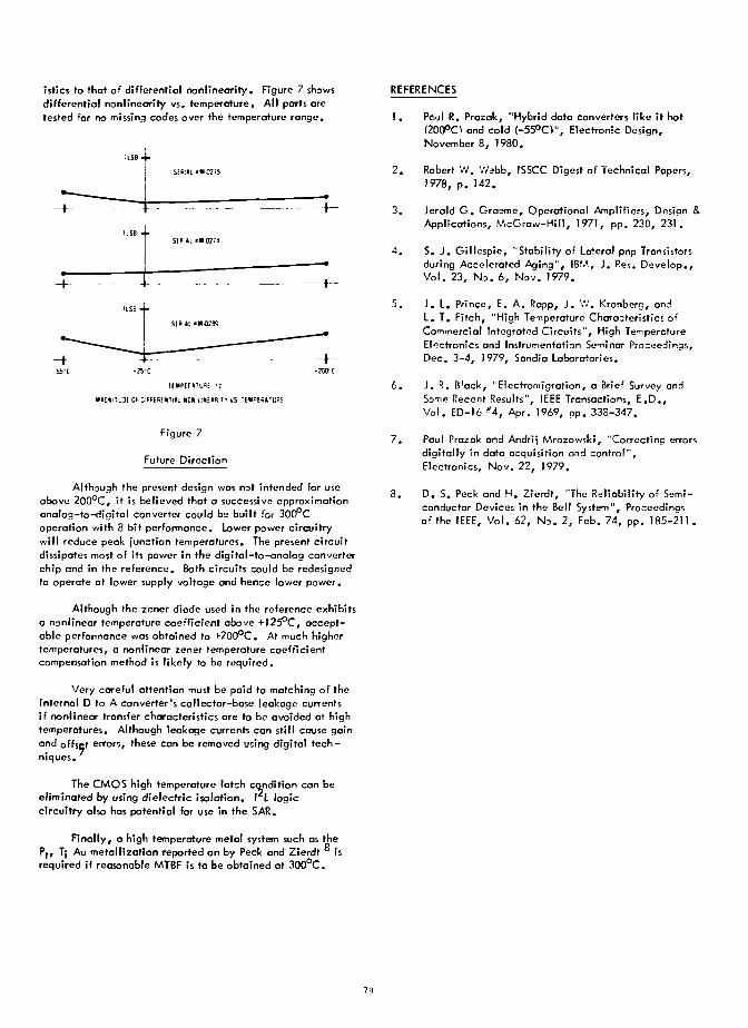
istics to that of differential nonlinearity. Figure 7 showsdifferential nonlineorify vs. temperature. All parts aretested for no missing codes over the temperature range.
K«G«llu:t 01 C:HIR!«TI«l • 1 VS Ti«Fffi«!U«!
Figure 7
Future Direction
Although the present design was not intended for useabove 200°C, it is believed that a successive approximationonolog-to-digital converter could be built for 300°Coperation with 8 bit performance. Lower power circuitrywil l reduce peak junction temperatures. The present circuitdissipates most of its power in the digital-to-analog converterchip and in the reference. Both circuits could be redesignedto operate ct lower supply voltage and hence lower power.
Although the zener diode used in the reference exhibitsa nonlinear temperature coefficient above +}2$>Ct accept-able performance was obtained to *-200°C. At much highertemperatures, a nonlinear zener temperature coefficientcompensation method is likely to be required.
Very careful attention must be paid to matching of theinternal D to A converter's collector-base leakage currentsi f nonlinear transfer characteristics are to be avoided at hightemperatures. Although leakage currents can still cause gainand offset errors, these can be removed using digital tech-niques.
The CMOS high temperature latch condition can beeliminated by using dielectric isolation. I L logiccircuitry also has potential for use in the SAR.
Finally, a high temperature metal system such as thePf, T; Au metallization reported on by Peck and Zierdt isrequired if reasonable MTBF is to be obtained at 300°C.
REFERENCES
I . Pc/jl R. Prazak, "Hybrid data converters like i t hot(200°O and cold (-55°CV, Electronic Design,November 8, 1980.
2. Robert W. V/^bb, ISSCC Digest of Technical Papers,1978, p. 142.
3. Jerald G . Graeme, Operational Amplifiers, Design &Applications, McGraw-Hill, 1971, pp. 230, 231.
4 . S. J . Gillespie, "Stability of Lateral pnp Transistorsduring Accelerated Aging", IBM, J . Res. Develop.,Vol . 23, No. 6, Nov. 1979.
5. J . L. Prince, E. A. Rapp, J . \V. Kronberg, andL. T. Fitch, "High Temperature Characteristics ofCommercial Integrated Circuits", High TemperctureElectronics and Instrumentation Seminar Proceedings,Dec. 3-4, 1979, Sandio Loborcfones.
6. J . R. B'ack, "Electromigration, a Brief Survey andSome Recent Results", IEEE Transactions, E.D.,Vol . ED-16 *4 , Apr. 1969, pp. 338-347.
7. Paul Prazak and Andrij Mrozowski, "Correcting errorsdigitally in data acquisition and control".Electronics, Nov. 22, 1979.
8. D. S. Peck and H. Zierdt, "The Reliability of Semi-conductor Devices in the Bell System", Proceedingsof the IEEE, Vol . 62, No. 2, Feb. 74, p p . 185-211.
79

50
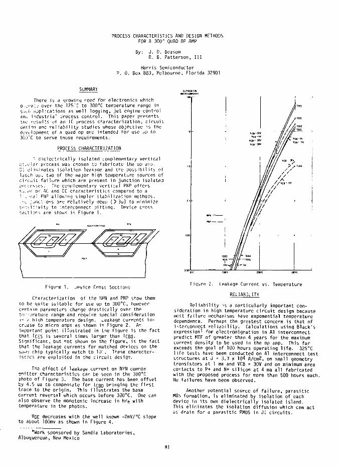
PROCESS CHARACTERISTICS AND DESIGN METHODSFOR A 300° QUAD OP AMP
By: J. D. BeasomR. B. Patterson, III
Harris SemiconductorP. 0. Box 883, Melbourne, Florida 32901
SUMMARY
There is a growing need for electronics whichO'jraLd over the 125^C to 300°C temperature range insu<_i' applications as well logging, jet engine controlan.i industrial process control. This paper presentstne results of an IC process characterization, circuitdesiin and reliability studies whose objective is thedevelopment of a quad op amp intended for use up to300"C to serve those requirements.
PROCESS CHARACTER!ZATJON
1 dielectrically isolated complementary verticalbi.,'jlar process was chosen to fabricate the op amp.Di eliminates isolation leakage and the possibility oflatch up, two of the major high temperature sources ofcircuit failure which are present in junction isolatedprocesses. The complementary vertical PNP offerssu.>t.'rior AC and DC characteristics compared to a1 t ral PNP allowing simpler stabilization methods.1 l-i_- .-unctions are relatively deep (> 3u) to minimizese-iiitivi ty to interconnect pitting. Device crosssections are shown in Figure 1.
Figure 1. uevice Cross Sections
Characterization of the NPN and PNP show themto be quite suitable for use up to 300°C, howevercertain parameters change drastically over thet'M''erature range and require special considerationin fl high temperature design. Leakage currents in-crease to micro amps as shown in Figure 2. Animportant point illustrated in the figure is the factthat ICES is several times larger than ICBO-Significant, but not shown on the figure, is the factthat the leakage currents for matched devices on thesai.i-:- chip typically match to 10' . These character-istics are exploited in the circuit design.
The effect of leakage current on NPN commonemitter characteristics can be seen in the 300°Cphoto of Figure 3. The base current has been offsetby 4.5 ua to compensate for IQBQ bringing the firsttrace to the origin. This illustrates the basecurrent reversal which occurs before 300°C. One canalso observe the monotonic increase in hfe withtemperature in the photos.
VcE decreases with the well known -2mV/°C slopeto about lOOmv as shown in Figure 4.
Fiqure 2. Leakage Current vs. Temperature
RELIABILITY
Reliability is a particularly important con-sideration in high temperature circuit design becausemost failure mechanisms have exponential temperaturedependence. Perhaps the greatest concern is that ofinterconnect reliability. Calculations using Black'sexpression' for electromigration in Al interconnectpredict MTF of greater than 4 years for the maximumcurrent density to be used in the op amp. This farexceeds the goal of 100 hours operating life. 325°Clife tests have been conducted on Al interconnect teststructures at J = 3.3 x 10⁴ A/cm2, on small geometrytransistors at 1 ma and VCB = 30V and on minimum areacontacts to P+ and N+ silicon at 4 ma all fabricatedwith the proposed process for more than 500 hours each.No failures have been observed.
Another potential source of failure, parasiticMOS formation, is eliminated by isolation of eachdevice in its own dielectrically isolated island.This eliminates the isolation diffusion which can actus drain for a parasitic PMOS in JI circuits.
*Work sponsored by Sandia Laboratories,Albuquerque, New Mexico
81
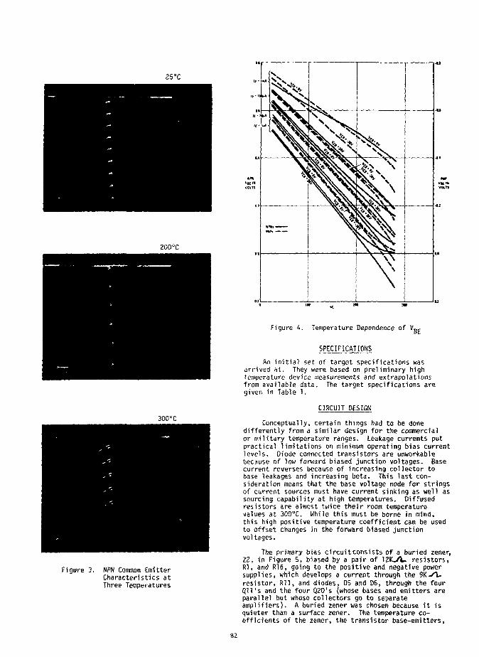
25 °C
200°C
300 °C
Figure 3. NPN Common EmitterCharacteristics atThree Temperatures
Figure 4. Temperature Dependence of V.BE
SPECIFICATIONS
An initial set of target specifications wasarrived at. They were based on preliminary hightemperature device measurements and extrapolationsfrom available data. The target specifications aregiven in Table 1.
CIRCUIT DESIGN
Conceptually, certain things had to be donedifferently from a similar design for the commercialor military temperature ranges. Leakage currents putpractical limitations on minimum operating bias currentlevels. Diode connected transistors are unworkablebecause of low forward biased junction voltages. Basecurrent reverses because of increasing collector tobase leakages and increasing beta. This last con-sideration means that the base voltage node for stringsof current sources must have current sinking as well assourcing capability at high temperatures. Diffusedresistors are almost twice their room temperaturevalues at 300°C. While this must be borne in mind,this high positive temperature coefficient can be usedto offset changes in the forward biased junctionvoltages.
The primary bias circuitconsists of a buried zener,Z2, in Figure S, biased by a pair of 12K./L. resistors,Rl, and R16, going to the positive and negative powersupplies, which develops a current through the 9K>T-resistor, Rll, and diodes, 05 and D6, through the fourqil's and the four Q20's (whose bases and emitters areparallel but whose collectors go to separateamplifiers). A buried zener was chosen because it isquieter than a surface zener. The temperature co-efficients of the zener, the transistor base-emitters,
82
and the diodes approximately cancel the temperaturecoefficient of the resistor, Rll, keeping the currentdelivered to the positive and negative current sourcebase nodes approximately constant over the temperaturerange.
The input stage of the amplifier consists of thedifferential PNP pair, Q21 and Q22, along with Q16, Q17and R13 (which make up a leakage current compensationnetwork) and the current source consisting of Q5 andR4. PNP devices were chosen for the input pair becausetheir collector to base leakage is significantly lowerthan that of the NPN devices. R13 provides most of thecollector base voltage for Q16 and Q17 whose ICBO'scancel those of Q21 and Q22 to within the limits oftheir match. The collectors of Q21 and Q22 go to thefollowing stage which consists of Q26 and Q27.
NPN transistors Q26 and Q27 along with R18 and R19constitute grounded base stages. They translate thesignal toward the positive side of the circuit. Thestage consisting of Q27 and R19 shields the inputdevice, Q22, from the large voltage excursions of thehiah impedance node to which its collector is common.The collector of Q26 drives the current mirror stage.
The current mirror consists of Q2, Q3, Q7, Q8,Q12, JI3, Dl , 02, D3, D4, Zl and R3. The primary partof the mirror consists of Q7, Q8 and Q13. Q12 is addedto make the collector to base voltage of Q7 equal touhat of Q8. This removes a small offset problem due tohrb effects but (more importantly in this case)
TABLE 1
TARGET SPECIFICATIONS AND
ParameterOffset Voltage
Avu. OffsetVoltane Drift
Input BiasCurrent
I.vi'L OffsetCurrent
CoisiMon Mode
Input Range
DifferentialInput Signal
Coiiii-iun M o d e
Rejection Ratio
Voltage Gain
ChannelSeparation
Gain bandwidth
Output VoltageSwing
Slew Rate
Output Current
Power SupplyRejection Ratio
Temperature
25'
25'
25"
25'
25°C
300°CX to 300°C
300°C
300°C
X to 300°C
'C to 300°C
300°C
300°C
300°C
300°C
'C to 300°C
300°C300°C
300°C
BREADBOARD
Limit
3.0 <
6.0<10 <
5 <
1.3<
>+10
7<
>60
>"0
?80
>3
>±10
>±2
5<
>60
RESULTS
BB
0.2
-5.320
2.1
3.4
'13.9
71.7
71.9
13.7
71.7
Units
mV
mVuV/°C
uA
uA
V
V
dB
dB
dB
MHz
V
V/usecmA
dB
Noise 25°C V/VHZ
equalizes the collector base leakages of Q7 and Q8.Ordinarily, Q8 and Q12 would be connected as trans-diodes but, because the forward biased junctionvoltages are so low at high temperatures, D2 and D3 areused to tie the base to the collector of Q8 and Zl isused to tie the base to the collector of Q12. At lowtemperatures D2 and D3 are forward biased by the basedrive requirements of Q7 and Q8 as Zl is reverse biasedby the base drive requirements of Q12 and Q13. At hightemperatures Q2 and Q3 supply ICES to forward bias D2and D3 and reverse bias Zl as well as supply the re-versed base current of Q7 and Q8 and of Q12 and Q13.Dl and D4 provide a voltage drop equal to D2 and D3 tomake the voltage across Q2 more nearly the same as thatacross Q3. R3 provides most of the voltage for Q3(and, therefore, Q2). The collector of Q13 is commonwith the high impedance node.
The next stage consists of a complementary pair ofemitter followers, Q15 and Q18, biased by currentsources consisting of Q6 and R5 and of Q28 and R20respectively. There is also a leakage current com-pensation network associated with each follower con-sisting of Q9 and R7 for Q15 and Q24 and R14 for Q18.The bases of Q15 and Ql8 are common to the highimpedance node. Difference in ICBO between Q15 and Q18at high temperature would be refleLi.ed tc the- amun'u-rinput as an offset.
No special design considerations because of hightemperature were necessary in the output stage designwhich consists of qi4 and Q19 driven by Q15 and Q18respectively.
The positive and negative current source basenodes remain to be discussed. The positive node is setup by Q4 and R2. Emitter follower Q10 supplies thebase drive requirements of Q4, Q5 and Q6 until thebase currents reverse at high temperature. Then theyare supplied by Ql's ICES whose excess is then suppliedby the emitter follower. This excess flowing throughR6 and Q10 provides some collector to base voltage forQ4. ICES seems to be a minimum of three times ICBO at300°C so Ql is made a double sized device because threesources of ICBO (one of them, Q5, is double sized) haveto be supplied by it along with excess for the emitterfollower. The same considerations apply to thenegative node which is set up by Q25 and R17. Q23serves as the emitter follower, Q29 the source of ICESand Q25, Q26, Q27 and Q28 receive their base drive fromthe node.
BREADBOARD
In order to test the validity of the design it wasbreadboarded using four subcircuit chips made from anexisting circuit by custom interconnect patterns. Aschematic of the breadboard is shown in Figure 6. Thepackage pins are designated as follows. The firstnumber designates the type of package then there is adash and the second number designates the pin on thatpackage type. Package type 1 contained the primarybias circiiitry. Package type 2 contained the negativebias circuitry. Package type 3 contained the inputstage and positive bias circuitry. Package type 4contained the current mirror and output circuitry.
Several breadboards made up of packaged sub-circuits were socket mounted inside an oven door,externally connected as in Figure 6 and tested overtemperature. Results are shown in Table 1.
83
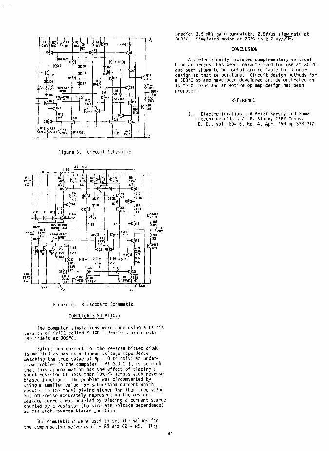
predict 3.5 MHz gain bandwidth, 2.6V/US slew rate atSOO°C. Simulated noise at 25°C is 8.7 nv/-fHz".
CONCLUSION
A dielectrically isolated complementary verticalbipolar process has been characterized for use at 300°Cand been shown to be useful and reliable for lineardesign at that temperature. Circuit design methods fora 300°C op amp have been developed and demonstrated on1C test chips and an entire op amp design has beenproposed.
REFERENCE
1. "Electromigration - A Brief Survey and SomeRecent Results", J. R. Black, IEEE Trans.E. D., vol. ED-16, No. 4, Apr. '69 pp 338-347.
Figure 5. Circuit Schematic
Figure 6. Breadboard Schematic
COMPUTER SIMULATIONS
The computer simulations were done using a Harrisversion of SPICE called SLICE. Problems arose withthe models at 300°C.
Saturation current for the reverse biased diodeis modeled as having a linear voltage dependencematching the true value at Vp = 0 to solve an under-flow problem in the computer. At 300cC Is is so highthat this approximation has the effect of placing ashunt resistor of less than lOK-ZL across each reversebiased junction. The problem was circumvented byusing a smaller value for saturation current whichresults in the model giving higher VBE than true valuebut otherwise accurately representing the device.Leakage current was modeled by placing a current sourceshunted by a resistor (to simulate voltage dependence)across each reverse biased junction.
The simulations were used to set the values forthe compensation networks Cl - R8 and C2 - R9. They
84
HYBRID A/D CONVERTER FOR 200°C OPERATION
Mark R. Sul1ivan
Jeffrey B.TothMicro Networks Company
32U Clark StreetWorcester, Massachusetts 01606
ABSTRACT
This paper describes the design and development of a h i >qh performance hybrid 12
which will operate reliably at 200°C. A product of this type was found to be ne
geothermal probing, oil-well logging, jet engine and nuclear reactor monitorino,
the environments may reach temperatures of up to 200°C. This product represents
as it proved the operation of integrated circuits at high temperature, as well
both the electrical and mechanical reliability of hybrid circuits at 200°C. Bee
A/D converter involved both digital and linear circuitry, this produced an oppor
performance of both technologies at 200°C. Initial mechanical failure modes led
methods of wire bonding and die attachment. The result of this work was a 12 bi
operate at 200°C with .05'' linearity, 1 £ accuracy, 350 uSec conversion time, an
This product also necessitated the development of a unique three metal system in
done utilizing aluminum bonding pads, gold wire bonding to all gold areas, and e
between gold and aluminum connections. This sytem totally eliminates the format
bonding interface which can lead to bond failure.
bit analog to digital converter,
cessary in areas such as
and other applications where
an advancement in electronics
as providing information about
ause the circuit desiqn of the
tjnity to evaluate the
to researching more reliable
t A/D converter which will
d only ^55mW power consumption.
which aluminum wire bond 1nq is
inployment of J nickel interface
ion of intermetal1ics at the
INTRODUCTION
Recently the electronics industry has been made aware
of the need for electronic components and systems which
will operate at temperatures as high as 200°C. These
applications include geothermal probing, oil well
logging, jet engine and nuclear reactor monitoring ?nd
other hostile environments where the temperature may
reach 200°C or higher. In some of these applications,
as in oil well logging and geothermal probing, it is
necessary to transmit data through long lengths of
cable which run from deep into the earth to the sur-
face.' These applications are where a high tempera-
ture A to D converter becomes highly desirable. Trans-
mitting low level analog data over a long distance
such as this would be very difficult without intro-
ducing significant extraneous errors. Through the
use of an A to D converter it becomes possible to take
outputs from strain gauges and thermocouples, convert
them to "ones" and "zeros" and then transmit this data
digitally to the surface.
ADVANTAGES OF HYBRIDS
An A to D converter can be fabricated in many differ-
ent forms such as a module, printed circuit board, or
hybrid circuit. Hybrid reliability at 125°C has been
proven to be excellent through many thousands of hours
of qualification tests. This reputation makes hybrid
technology a wise choice for 200°C operation. A
hybrid circuit can contain several different i.C.s in
one small package, which is advantageous in applica-
tions where space is limited.
A TO D CIRCUIT DESIGN
An A to D converter proved to be a challenging
product to design and evaluate at 200°C due to the
fact that little information concerning the different
types of components and their properties at high
temperature was available. Passive components, such
as resistors and capacitors and active components
including transistors and integrated circuits required
extensive analysis and evaluation. The final A/D
design employs both linear and digital circuitry.
In the design of the HN57OO, reliability was consid-
ered of prime importance. Two factors that signifi-
cantly effect the reliability of any circuit are
power and level of complexity. Research in high
temperature electronics has shown that the rate of
aging, those factors that produce chanqes in para-
meter of key components, will approximately double
with each 10°C temperature rise.2
For a hybrid circuit the substrate temperature will
increase as the power consumption increases. As a
design goal the typical substrate to ambient temper-
ature rise was not to exceed IO°C. The 32 pin double
PIP Package, selected primarily for its form factor,
has a typical substrate to ambient rise of 27°C/Watt.^
Thus to keep this rise under 10°C, the lypii.al
power consumption was limited to 311 milliwatts. To
reduce the complexity, as few I.C.s were used as
possible.
There are several different approaches to A to D
conversion which are currently used. The MN57OO uses
the successive approximation method. This allows a
converter to be made using few components and has
good characteristics in speed, resolution, and
accuracy. A successive approximation A to D converter
consists of four sections, D to A converter, reference,
comparator, and successive approximation register
( SAR). See Figure 1. Each of these sections will
be discussed showing the design considerations for
200°C operation.
D to A Converter
The D to A section of the MN57OO utilizes a voltage
switching R-2R ladder network. The switch is CMOS
and connects each leg of the ladder either to ground
or a reference voltage. See Figure 2. A CMOS switch
was chosen because of its low power consumption and
evaluations showed it to be reliable at 200°C.
Reference
The reference circuit shown in Figure_3_ consists ofa temperature compensated zener diode and a dielec-trically isolated op-amp. The zener was found to beaccurate to about 10ppm/°C from 25°C to I25°C. From125°C to 200°C the temperature coefficient increasedto i40ppm/°C. Figure_Jt shows a graph of zenervoltage vs. temperature.
85
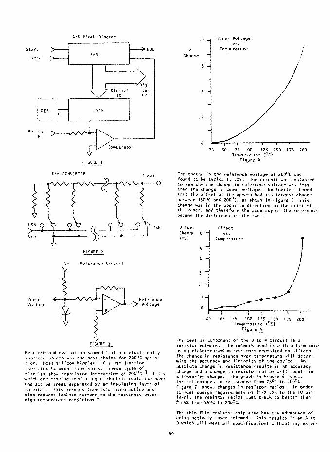
A/0 Block Diagram
EOC
FIGURE 1
D/A CONVERTER I out
MSB
Vref
FIGURE 2
V- Reference Circuit
VoltageReferenceVo)tage
FIGURE 3
Research and evaluation showed that a dielectricallyisolated op-amp was the best choice for 200°C opera-tion. Most silicon bipolar I.C.s use junctionisolation between transistors. These types ofcircuits show transistor interaction at 20Q°C.' I.C.swhich are manufactured using dielectric isolation havethe active areas separated by an insulating layer ofmaterial. This reduces transistor interaction andalso reduces leakage current to the substrate underhigh temperature conditions.
Change
•3 -4
.2 -i
Zener Voltagevs.
Temperature
75 100 125 150Temperature (°C)
Figure U
r175 200
The change in the reference voltage at 200°C wasfound to be typically .2^. The circuit was evaluatedto see why the change in reference voltage was lessthan the change in zener voltage. Evaluation showedthat the offset of the op-amp had its largest changebetween 150°C and 200°C, as shown in Figure_5_ Thischange was in the opposite direction to the drift ofthe zener, and therefore the accuracy of the referencebecame the difference of the two.
OffsetChange 6 —j(mV)
Offsetvs.
Temperature
25 50 75 100 125 150Temperature (°C)
Figure 5
175 200
The centra) component of the D to A circuit is aresistor network. The network used is a thin film chipusing nickel-chromium resistors deposited on silicon.The change in resistance over temperature will deter-mine the accuracy and linearity of the device. Anabsolute change in resistance results in an accuracychange and a change in resistor ratios will result ina linearity change. The graph in Figure_6^ showstypical changes In resistance from 25°C to 200°C.Figure_7_ shows changes in resistor ratios. In orderto meet design requirements of ±1/2 LSB to the 10 bitlevel, the resistor ratios must track to better thani.05% from 25°C to 200°C.
The thin film resistor chip also has the advantage ofbeing actively laser trimmed. This results in an A toD which will meet all specifications without any exter-
86
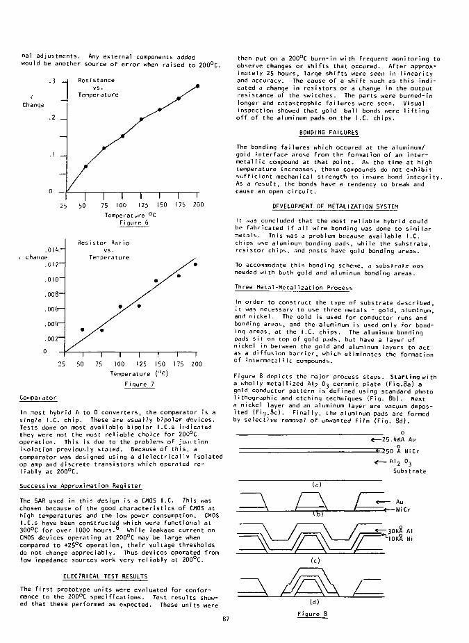
nal adjustments. Any external components addedwould be another source of error when raised to 200°C.
Change
.1 —
0 -
I I T \ 1 \25 50 75 100 125 150 175 200
Temperature °C
Figure 6
.014-
chanqe
.012'
.010—
.008-
.006—
.004—
.002-
0
Res i stor Rat io
vs.
Temperat ure
25 50 75
1 1
100 125
Temperature
Figure 7
I150
(°r.)
i
175 200
Comparator
In most hybrid A to D converters, the comparator is a
single I.C. chip. These are usually bipolar devices.
Tests done on most available bipolar I.C.s indicated
they were not the most reliable choice for 200°C
operation. This is due to the problems of junction
isolation previously stated. Because of this, a
comparator was designed using a dielectricallv isolated
op amp and discrete transistors which operated re-
liably at 200°C.
Successive Approximation Register
The SAR used in this design is a CMOS I.C. This was
chosen because of the good characteristics of CMOS at
high temperatures and the low power consumption. CMOS
I.C.s have been constructed which were functional at
300°C for over 1000 hours. While leakage current on
CMOS devices operating at 200°C may be large when
compared to +25°C operation, their voltage thresholds
do not change appreciably. Thus devices operated from
low impedance sources work very reliably at 200°C.
ELECTRICAL TEST RESULTS
The first prototype units were evaluated for confor-
mance to the 200°C specifications. Test results show-
ed that these performed as expected. These units were
then put on a 200°C burn-in with frequent monitoring to
observe changes or shifts that occured. After approx-
imately 25 hours, large shifts were seen in linearity
and accuracy. The cause of a shift such as this indi-
cated a change in resistors or a change in the output
resistance of the switches. The parts were burned-in
longer and catastrophic failures were seen. Visual
inspection showed that gold ball bonds were lifting
off of the aluminum pads on the I.C. chips.
BONDING FAILURES
The bonding failures which occured at the aluminum/
gold interface arose from the formation of an inter-
metallic compound at that point. As the time at high
temperature increases, these compounds do not exhibit
sufficient mechanical strength to insure bond integrity.
As a result, the bonds have a tendency to break and
cause an open circuit.
DEVELOPMENT OF METALIZATION SYSTEM
It was concluded that the most reliable hybrid could
be fabricated if all wire bonding was done to similar
metals. Tnis was a problem because available I.C.
chips use aluminum bonding pads, while the substrate,
resistor chips, and posts have gold bonding areas.
To accommodate this bonding scheme, a substrate was
needed with both gold and aluminum bonding areas.
Three Metal-Metalization Process
In order to construct the type of substrate described,it was necessary to use three metals - gold, aluminum,and nickel. The gold is used for conductor runs andbonding areas, and the aluminum is used only for bond-ing areas, at the I.C. chips. The aluminum bondingpads sit on top of gold pads, but have a layer ofnickel in between the gold and aluminum layers to actas a diffusion barrier, which eliminates the formationof intermeto11ic compounds.
Figure 8 depicts the major process steps. Starting with
a wholly metallized AI2 O3 ceramic plate (Fig.8a) a
gold conductor pattern is defined using standard photo
lithographic and etching techniques (Fig. 8b). Next
a nickel layer and an aluminum layer are vacuum depos-
ited (Fig.8c). Finally, the aluminum pads are formed
by selective removal of unwanted film (Fig. 8d).
-25.4KA Ai.o
3 5 0 A NiCr
— Al 2 0,
Substrate
(d)
87
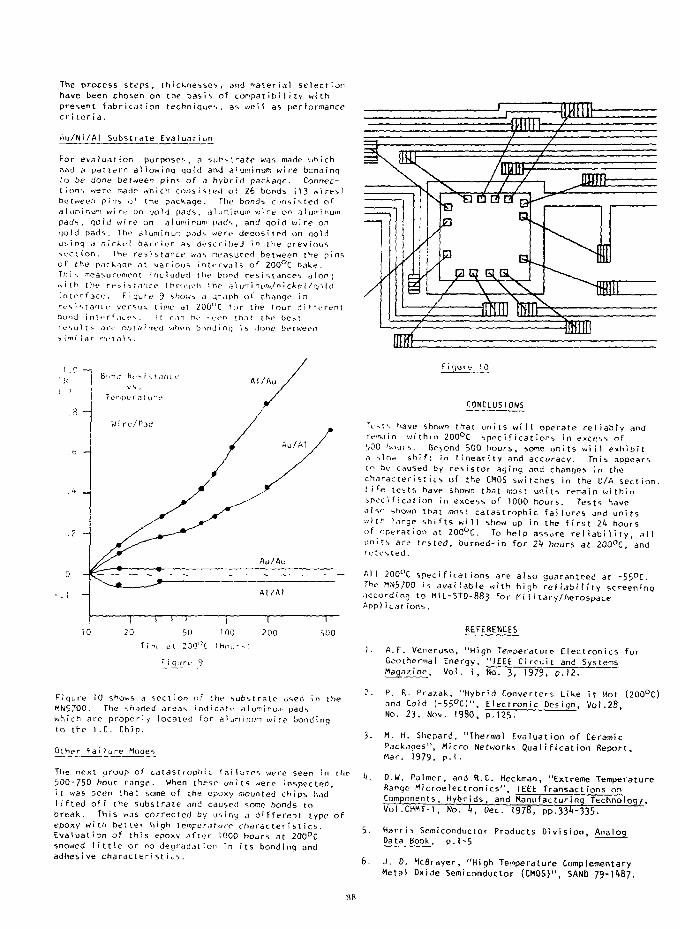
The process steps, thicknesses, and materiai select ionhave been chosen on the basis of compat i b i\ ity withpresent fabri cjt ion tecbn iques , as welt as performancecri teria.
Mu/Ni/AI Substrate Eva Iuat run
For evaIuation purposes, a 5uh^'-ate was made whichhod a pattern ai'owinq qofd and a'ominum wire bendingto be done between pins of a hybrid packaqe. Connec~I I ons were made wh ich cons isted of 26 bonds (13 wi res)be tween pins of the package . The bonds curis f s ted ofa I un i num wi rt1 on go Id pads » t) i ui'U nutv» «' re on ^} tie* i numpads , qo 1 d wf re on al uni nun. pads , and qoi d wl re on<\JO I d pads . The a I unii nun pads were depos i ted on qol dusing ,3 nickel barrier ^ described in the previouss vet. ion. The resistance was neasured between the pinsof the p a t M q e at various intervals of 200°C bake.Th i s measurement i nc 1 uded t he bond res i stances alor-;w i t h t he re-s i s tance through X he o \ urni num/nicke ! /qnldinw-rface. Figure 9 showi a ^r.iph of change inresistance versus tine <it 200"C tor the foubond i nttT f.ii.e*', It c m br n-en t h.-j ( the b e Mresults are ob I ct' ned vjhun bond i n q is done be t ween•a i m i tar fit11 a t s .
i .0
different
120
Ti
1
f
1
at
i Hi
150
:oo"c
,/rt. 9
1100
( H o u r s )
1200
1iOO10
Fiqure 10 shows a section of the substrate used in theM^57OO. The shaded areas indicatt- ^lurpinuin padswhich are properly located for aluninum wire bondingto tt-e I.E. Chip.
Other Failure Modes
The next group of catastrophic failures were seen in the500-750 hour range. When these units were inspected,it was seen that some of the cpoxy mounted chips hadlifted off the substrate and caused s o w bonds tobreak. This was corrected by usiny a different type ofepoxy with better liicjh temperature characteristics.Evaluation of this epoxv after 1000 hours at 200°Cshowed little or no degradation in its bonding andadhesive characteristics.
10
CONCLUSIONS
Test>. have shown that units will operate reliably andrviain within 200°C specifications in excess of'j00 hours. Bejond 500 hours, some units will exhibit,i slow shift in linearity and accuracy. This appearst" be caused by resistor aging and changes in thecharacteristics of the CMOS switches in the D/A section.Li fe tests have shown that most units remain withinspecification in excess of 1000 hours. Tests havealso .,hown that most catastrophic failures and unitswith targe shifts will show up in the first 2h hoursof operation at 200°C. To help assure reliability, allunits are tested, burned-in for 2k hours at ZOO°C, andi e t e s t e d .
All 200°C s p e c i f i c a t i o n s are a l s o g u a r a n t e e d at -55°C.The M N 5 7 O O is a v a i l a b l e w i t h h i g h reliability s c r e e n i n gaccording to HIL-STD-883 for Military/AerospaceApplicat ions.
REFERENCES
1. A.f. Veneruso, "High Temperature Electronics forGeothermal Energy, "IEEE Circuit and SystemsMagazine, Vol. 1, No. 3, 1979, p.12.
2. P. R. Prazak, "Hybrid Converters Like it Hot (200°C)and Cold (-55°C)", Electronic Design, Vol.28,No. 23. Nov. I960, p.125, "
3. M. H. Shepard, "Thermal Evaluation of CeramicPackages", Micro Networks Qualification Report,Mar. 1979, p.I.
h. O.W. Palmer, and R.C. Heckman, "Extreme TemperatureRange Microelectronics", IEEE Transactions onComponents, Hybrids, and Manufacturing Technology,Vol.CHMT-l, No. 4, Dec. 1978, pp.33<4-?35.
5. Harris Semiconductor Products Division,Data Book, p.1-5
Analog
6. J. D. McBrayer, "High Temperature ComplementaryMetal Oxide Semiconductor (CMOS)", SAND 79-1487.
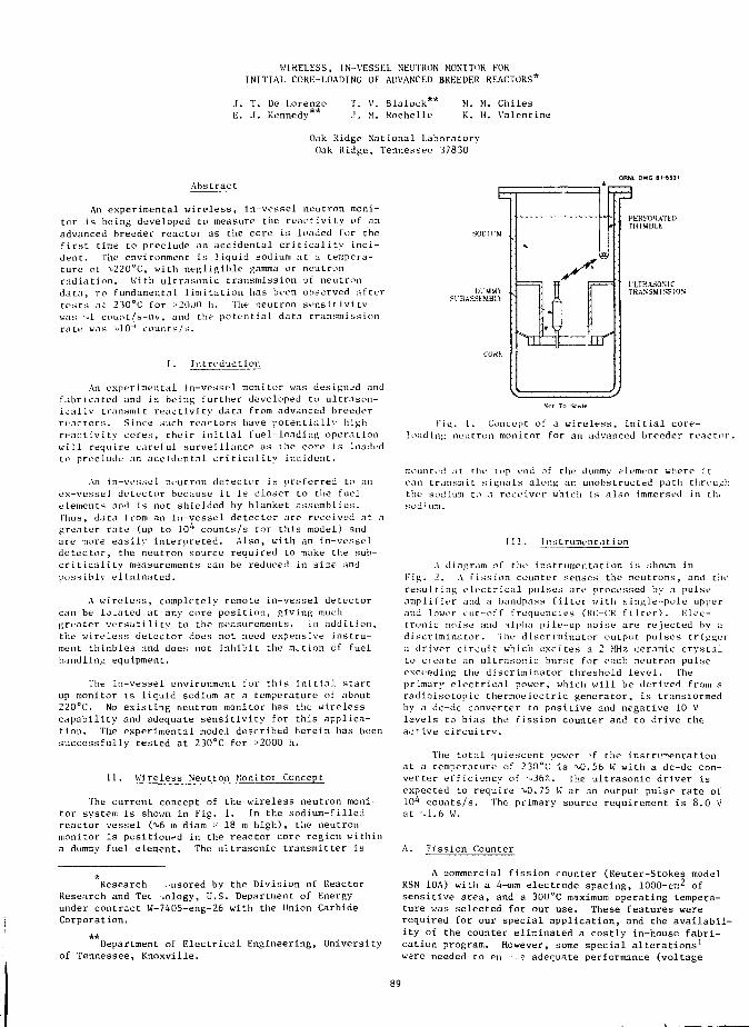
WIRELESS, IN-VESSEL NEUTRON MONITOR FORINITIAL CORE-LOADING OF ADVANCED BREEDER REACTORS'*
J. 1. De LorenzoL. J. Kennedv
T. V. Blalock**J- M. Rochelie
M. M. ChilesK. H. Valentine
Oak Ridge National LaboratoryOak Ridge, Tennessee 37830
Abstract
An experimental wireless, in-vessel neutron moni-tor is being developed to measure the reactivity of anadvanced breeder reactor as the core is loaded for thefirst time to preclude an accidental criticality inci-dent. The environment is 1iquid sodium at a tempera-ture of %220°C, with negligible gamma or neutronradiation. With ultrasonic transmission of neutrondata, ro fundamental limitation has been observed nftertests aC 230°C for >20O0 h. The neutron sensitivitywas ' 1 cou:it/s-nv, and the potential data transmi ss ionrate was - 10"1 counts/s.
I . Introduction
An experimental in-vessel monitor was designed andfabricated and is being further developed to ultrason-ical ly transmi t rtactivi ty data from advanced breederreactors. Since such realtors have potentially highreactivity cores, their initial fuel-loading operationwill require careful surveillance as the core is loadedto preclude an accidental criticality incident.
An in-vessel neutron detectur is preferred to anex-vessel detec tor because it is closer to the fuelelements and is not shielded by blanket assemblies.Thus, data t rom an in-vessel detector are received at agreater rate (up to 10^ counts/s for this model) andare more easily interpreted. Also, wi th an in-vesseldetector, the neutron source required to make the sub-criticality measurements can be reduced in size andpossibly eliminated.
A wi reless, completely remote in-vessel detectorcan be located at any core position, giving muchgreater versatili ty to the measurements. in additi on,the wireless detector does not need expensive instru-ment th imbles and does not inhibi t the nu tion of fuelhandling equipment.
The in-vessel environment for this initial start-up monitor is liquid sodium at a temperature of about220°C. No existing neutron monitor has the wirelesscapability and adequate sensitivity for this applica-tion. The experimental model described herein has beensuccessfully tested at 230°C for >2000 h.
II. Wireless Neutron Monltox Concept
The current concept of the wireless neutron moni-tor system is shown in Fig. 1. In the sodium-filledreactor vessel ( 6 in diam '•< 18 m high) , the neutronmonitor is positioned in the reactor core region withina dummv fuel element. The ultrasonic transmitter is
Er
SODH'M
1)1 MM^
COKE3=z
•
OFtNL DWG 81-5531
P E R F O W A T K DTHIMBLE
ULTRASONICTRANSMISSION
Research -nsored by the Division of ReactorResearch and Tec iology, U.S. Department of Energyunder contract W-7405-eng-26 with the Union CarbideCorporation.
Department of Electrical Engineering, Universityof Tennessee, Knoxville.
l-'iu. 1. Concept of a wireless, ini t ial core-load ing neutron monitor for an advanced breeder reactor.
mounted at the tup end of the dummy element where i tfan transmit s ignals along an unobstructed path throughthe sod iurn to a receiver which is also immerst'd in th*sodi urn.
III. I r.strumentat ion
A diagram oi~ the instrumentation is shown inFig. 2. A f iss ion counter senses the neutrons, and theresulting electrical pulses are processed by a pulseamp 1i fier and a bandpass filter with single-pole uppurand lower cut-off !ruquenci i?s (KC-CR f i lter) . Elec-tronic noi se and ilpha pile-up noise are rejected by adiscriminator. The discr iminator output pulses triggera driver circui L wh Lch exci tes a 2 MHz ceramic crystalto cieate an ultrasonic burst for each neutron pulweexceeding the discr iminator threshold level. Thepr imary electrical power, which will be derived from aradioisotopic thermoelectric generator, is transformedby a dc-dc converter to positive and negative 10 Vlevels to bias the fission counter and to drive theactive circuitry.
The total quiescent power >f the instrumentationat a temperature of 23O°C is 0.56 W with a dc-dc con-verter efficiency of ^36%. The ultrasonic driver isexpected to require ^0.75 W at an output pulse rate of10^ counts/s. The primary source requirement is 8.0 Vat vl.6 W.
A. Fission Counter
A commercial fission counter (Reuter-Stokes modelRSN-10A) with a 4-mm electrode spacing, 1000-cm^ ofsensitive area, and a 300°C maximum operating tempera-ture was selected for our use. These features wererequired for our special application, and the availabil-ity of the counter eliminated a costly in-house fabri-cation program. However, some special alterations1
were needed to en -.° adequate performance (voltage
89
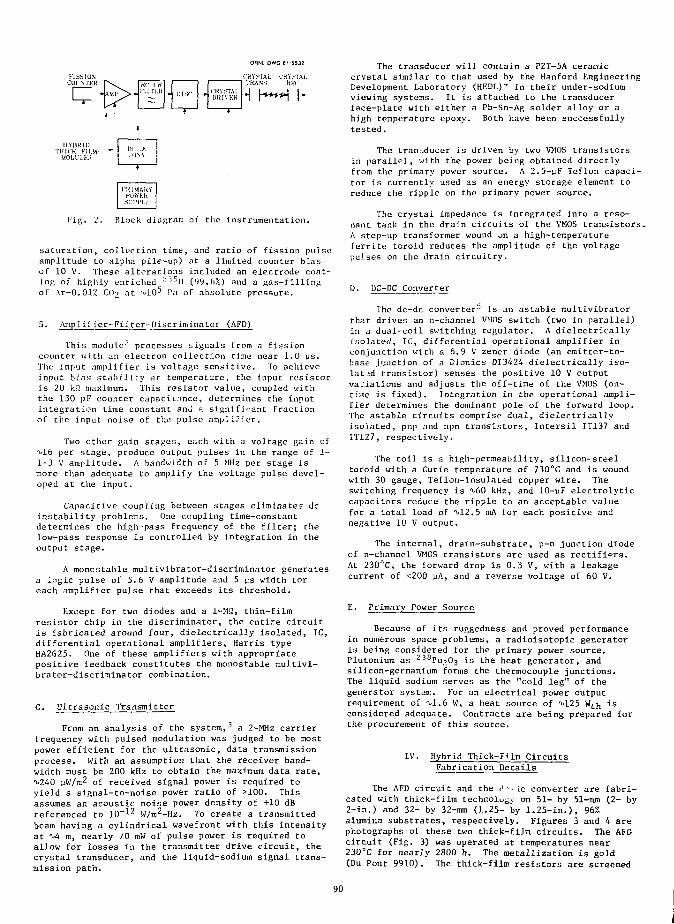
V'.L n.H 111SC -Cfn.STAIDRIVKR
OflNL DWG 81-5532
CRYSTAL CKVSTATK^NS RKf
HYISHIDT H I C K KI1.M-
MOD
•- DC DC
I'KlMAiiYKHVERsrm.y
Fig. 2. Block diagram of the instrumentation.
saturation, collection time, and ratio of fission pulseamplitude to alpha pile-up) at a limited counter biasof 10 V. These alterations included an electrode coat-Lnfi of highly enriched 235U (99.6%) and a gas-fillingof Ar-0.01% C(>2 at ^lO^ Pa of absolute pressure.
B. Amplifier-Filter-Discriminator (AFP)
This module2 processes bignals from a fissioncounter with an electron collection time near 1.0 ps.The input amplifier is voltage sensitive. To achieveinput bins stability at temperature, the input resistoris 20 k£2 maximum. This resistor value, coupled withthe 130 pF counter capaciL.tnce, determines the inputintegration Lime constant and a significant fractionof the input noise of the pulse amplifier.
Two other gain stages, each with a voltage gain of^16 per stage, produce output pulses in the range of 1-1-J V amplitude. A bandwidth of 5 MHz per stage ismore than adequate to amplify the voltage pulse devel-oped at the input.
Capacitive coupling between stages eliminates dcinstability problems. One coupling time-constantdetermines the high-pass frequency of the filter; thelow-pass response is controlled by integration in theoutput stage.
A monostable multivibrator-discriminator generatesa logic pulse of 5.6 V amplitude and 5 us width foreach amplifier pulse that exceeds its threshold.
Except for two diodes and a 1-MS2, thin-filmresistor chip in the discriminator, the entire circuitis fabricated around four, dielectrically isolated, IC,differential operational amplifiers, Harris typeHA2625. One of these amplifiers with appropriatepositive feedback constitutes the monostable multivi-brator-discriminator combination.
C. Ultrasonic Transmitter
From an analysis of the system,3 a 2-MHz carrierfrequency with pulsed modulation was judged to be mostpower efficient for the ultrasonic, data transmissionprocess. With an assumption that the receiver band-width must be 200 kHz to obtain the maximum data rate,^240 iiW/m? of received signal power is required toyield a signal-to-noise power ratio of >100. Thisassumes an acoustic noise power density of +10 dBreferenced to lO"-^ w/m^-Hz. To create a transmittedbeam having a cylindrical wavefront with this intensityat ^4 m, nearly 70 mW of pulse power is required toallow for losses in the transmitter drive circuit, thecrystal transducer, and the liquid-sodium signal trans-mission path.
The transducer will contain a PZT-5A ceramiccrystal similar to that used by the Hanford EngineeringDevelopment Laboratory (HEDL)1* in their under-sodiumviewing systems. It Is attached to the transducerface-plate with either a Pb-Sn-Ag solder alloy or ahigh temperature epoxy. Both have been successfullytested.
The tranbducer is driven by two VMOS transistorsin parallel, with the power being obtained directlyfrom the primary power source. A 2.5-JJF Teflon capaci-tor is currently used as an energy storage element toreduce the ripple on the primary power source*
The crystal impedance is integrated into a reso-nant tank in the drain circuits of the VMOS transistors.A step-up transformer wound jn a high-temperatureferrite toroid reduces the amplitude of the voltagepulses on the drain circuitry.
D. DC-DC Converter
The dc-dc converter5 is an astable multivibratorthat drives an n-channel VMOS switch (two in parallel)in a dual-coil switching regulator. A dielectricallyisolated, IC, differential operational amplifier inconjunction with a 6.9 V zener diode (an emitter-to-base junction of a Dionics DI3424 dielectrically iso-latid transistor) senses the positive 10 V outputvariations and adjusts the off-time of the VMOS (on-time is fixed). Integration in the operational ampli-fier determines the dominant pole of the forward loop.The astable circuits comprise dual, dielectricallyisolated, pnp and npn transistors, Intersil IT137 andIT127, respectively.
The coil is a high-permeability, silicon-steeltoroid with a Curie temperature of 73O°C and is woundwith 30 gauge, Teflon-insulated copper wire. Theswitching frequency is -60 kHz, and 10-uF electrolyticcapacitors reduce the ripple to an acceptable valuefor a total load of 1/12.5 mA for each positive andnegative 10 V output.
The internal, drain-substrate, p-n junction diodeof n-channel VMOS transistors are used as rectifiers.At 230°C, the forward drop is 0.3 V, with a leakagecurrent of <200 uA, and a reverse voltage of 60 V.
E. Primary Power Source
Because of its ruggedness and proved performancein numerous space problems, a radioisotopic generatoris being considered for the primary power source.Plutonium as 238Pu^O3 is the heat generator, andsilicon-germanium forms the thermocouple junctions.The liquid sodium serves as the "cold leg" of thegenerator systotr.. For an electrical power outputrequirement of a.1.6 W, a heat source of ^125 Wtf, isconsidered adequate. Contracts are being prepared forthe procurement of this source.
IV. Hybrid Thick-Film CircuitsFabrication Details
The AFD circuit and the £•• - ic converter are fabri-cated with thick-film technology on 51- by 51-mm (2- by2-in.) and 32- by 32-mm (1.25- by 1.25-in.), 96%alumina substrates, respectively. Figures 3 and k arephotographs of these two thick-film circuits. The AFDcircuit (Fig. 3) was operated at temperatures near230°C for nearly 2800 h. The metallization is gold(Du Pont 9910). The thick-film resistors are screened
90
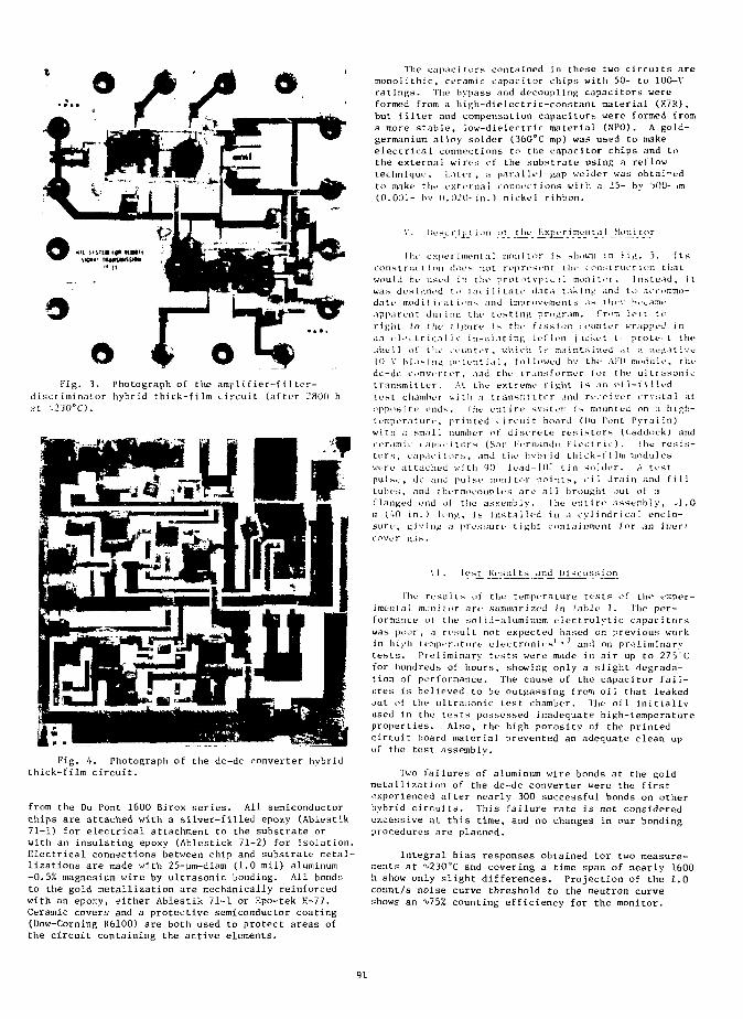
Fig. •). Photograph of the a m p l l f i e r - f i l t e r -di.scrimin.]tor hybrid th ick- f i lm i_ircuit (a f te r J800 h
______ ^Wi ^B ff f^K*
Fig. 4. Photograph of the dc-dc converter hybrid
thick-film circuit.
from the Du Pont 1600 Birox series. All semiconductor
chips are attached with a silver-filled epoxy (Ablestik
71-1) for electrical attachment to the substrate or
with an insulating epoxy (Ablestick 71-2) for isolation.
Electrical connections between chip and substrate metal-
lizations are made with 25-um-diam (1.0 mil) aluminum
-0.5% magnesium wire by ultrasonic bonding. All bonds
to the gold metallization are mechanically reinforced
with an epoxy, either Ablestik 71-1 or Epo-tek H-77.
Ceramic covers and a protective semiconductor coating
(Dow-Corning R6100) are both used to protect areas of
the circuit containing the active elements.
The capacitors contained in these two circuits are
monol i thi c , cframi c capac itor chips with 50- to 100—V
ratings. The bypass and de-coupling capacitors were
formed from a high-dielectrie-constant material (X7K),
but filter and compensation capacitors were formed from
a more stable, low-dieiectric material (NPO), A gold-
germanium alloy solder (360°C mp) was used to make
electrical connect ions to the capac i tor chips and to
the external wires of the substrate using a reflow
technique. Later, a para 1 lei gap welder was obtained
Lo make the external connections with a 25- by 500- nn
(0.001- bv 0.020-in.) nickel ribbon.
V . besc r ipt ion ol thy _Kx] e r i r?Le_n ta 1 _Mnni tor
i he- exper i mental mon i Lor is shown in H g. 3. Its
construe, t ion does not represent the c oust rue t ion Lh.it
would be used in the protnLvpie.il moil i Lor . 1 nstead, it
was des i/.ned to fac i 1 i tau% data t ak i n^ and to acrommu-
date mod i f i ca L i <>ns and improvement s as thev htv.i^e
apparent dur i n ; the test i ng program. VT^TT, lei t to
right in the figure is the- f i ssi on counter wrapped i n
an e l-'v.tr ica 1 ] v insuiat in;; Ief 1 on j .iuket 11 prote< t the
shel 1 ai' I he counter , whi ch i s ;na i nta ineii .it a nu.ia:. i ve
10 V bias ini; potent i a 1 , t'ol lowed bv the AFD module, the
dc-dc convert er , and the trans former 1 or t he ul t rason i i:
transmitter. At Lhe extreme ri>;l t iri an <nl-t'ilLed
test cliamlier wi t h a t ransmi tter and recoi ver crvsta 1 at
oppos i te ends . I he ent ire svsteir i s mountt.-d on a h igh-
tumperaturi1, printed circuit board (I>u Pont Pyra 1 in)
with r. sm.'il 1 number of d i sere to res is tors (.Caddock) and
re ram i i iapa. i tors (San Fernando K lectr ic ) . '1 he re si s-
tors, cap.'U- i tors, and the hvbrid thick-! i 1m modules
were attached with 90' lead-10' tin solder. A test
pu IM:', dc and pul se moni tor points, oil drai n and fill
tufies, and thermocouples are nil brought out of a
flanged end of the assembly. I he ent ire assembly, -1.0
in ('4O in. ) 1 ong , is ins Lai led in a cyl indr i ca 1 enclo-
sure , gi v i ng a pressure t i ,'lit enntai nment for nn inert
cover gas.
Vi . lest KesuJts and Discuss ion
The rusuIts oJ the tempera Lure tests of the exper-
iments ] m,:ni tor arv summarized in Table J . The per-
formance of the solid-aluminum electrolytic capacitors
was poor, .1 resul L not expected based on previ ous work
in high temperature electronics*"*7 and on prel iminary
tests. Preliminary tests were made in air up to 275°C
for hundreds of hours, showing only a siight degrada-
tion of performance. The cause of the capacitor fail-
ures is beiicved to be outgassing from oil that leaked
out of the ultrasonic test chamber. The oi1 initially
used in the tests possessed i nadequate high-temperature
properties. Also, the high porosity of the printed
circuit board material prevented an adequate clean up
of the test assembly.
Two failures of aluminum wire bonds at the gold
meta1li zat ion of the dc-dc converter were the first
experienced after nearly 300 successful bonds on other
hybrid circuits. This failure rate is not considered
excessive at this time, and no changes in our bonding
procedures are planned.
Integral bias responses obtained for two measure-
ments at ^23O°C and covering a time span of nearly 1600
h show only slight differences. Projection of the 1.0
count/s noise curve threshold to the neutron curve
shows an ^75% counting efficiency for the monitor.
91
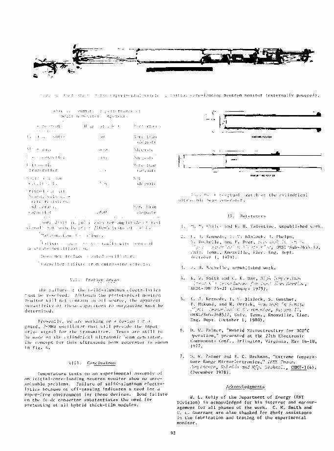
i « . . . - > ' : . : i r c . i r . i ; • : ' : • • r r : , . c K
H .n ii - J > ' i •!" ' IT... I",
i :vf: nviitron moni tor (external lv powered) .
- " > • • ; . . i i 1 1 i
I ! t i ] • • ( 11 U
i . MI1 . :; j r .
• i • t .
Vi
• ! i
i
I" I
I
d»
" •
I
•< -J
i t
I ,
- i i
11
<
n
-:.i <-•;•>[ ua 1 . K C I C!I u t th*.* i% v 1 i n d r i c a l,- tMU-ratur .
• nd . <-r.r- i . :-Vr, [h u- , i ; M » i I • - 1 j S u l l . i . i t M j u . i t <
^ 1 . - n . i 1 ' M ' I - t - < ; < i ; , \ - r i r . ' i l ! v l - | i ! f s t ^ . i t . ' ) U I .
' • ! . r - . I ' l l : , t i < n > L • ' i • i i i l t .
i . ! 1 1 u t « - . t \ . . . . ' . t \ ' 1 . u i 1 1 •. w i t i ' . ' H i t - I L
• u - ! : . ! < • ' M l i 1 ! i . ' . i t : " i .
! ' . < i - - : i t ' t i ! ! • 1 U i k I / l t r ( ! . i ^ t i I ! [ t . . f .
f . U ' - ' u i t < T i . i i i u n : r . ' n i m i l ; - . . ' - ^ : m - f i h , t s .
V I I . I ' r . i h l t - i i i A r r . i s
1 lu- I .i i 1 u i ' f I>1 t h e s ( -1 i d - a 1 unii num i-l u ^ L r . > 1 v t i c s
n u s L b e r i ' s o 1 v u d . A 11 h o u > : h Lhu p r o t u t v p i u.i 1 n t ' u t i o n
nii»n i t u r v i 11 no t . r o n t . i i ti . I TI o i l s o u r e t * , t h e u p p a r e n t
s e n s i t i v i LV c f t h t - s t - c.ip.ir i t c r s t o o u t ^ . i s s i n ^ m u s t b e
d e t e r m i IU'LI .
] ' r r . s e ; i L 1 y, v e . i r e w o r k i n g o n a d e s i . i ;" l o r .]
K ^ t t ' d , 2 - M H z cist; i L l a L o r t h a t w i l l p r o v i d e t h i ' i n p u t
d r i v e s i g n a l f o r t h e t r a n s m i L t e r . T e s t s a r e s t i l l t o
h e m a d e n n t h e e y 1 i n d r K : a 1 u 1 t r a s o n i c b e a m v,t-ne r a t o r .
Tiu' c o n c e p t l o r t l i i H u l t r a s u u i c h t -am ^ u n e r / i t u r i s s l u j v
VII1 . Ct^nclusions
Temperature tests on an exper imentn 1 assemh1y ofan initi.il-corc-loadlng neutron monitor show no unri—solvable problems. Fai J ure of solid-aluminum ei ectro-lytics because of off-gassing indicates a need for avapor-free environment for these devices. Bond failureon the dc-dc converter substantiates the need forpretesting of al l hybrid thick-film modules.
IX.
1. "•!. M. C i i i l t ^ a n d K. \i. \'a K-n t i n t - , u n p u b l i s h e d v n r k
J . I . I . Kf i in t 'dv , 1. V. B l a J n c k . I. I ' h t - l p s ,
V. K i ' e l i f l U - , nnd I-'. D v c r , ••..••. ;.••.••': .'>. '•• ••. %.." . ••• •• ' ; • ; ' . . - • . • . • • •: • ". •::•• •: ' V , ORNI / S u b - 7 M 4 . < U l ,
I ' IHV. U 'nn. , K n o x v i l l t , Klec. l'.np,. Di-'pt.(iicli.iH-r 1, 1979).
3. I. M. Koclit 'llf, unpubl ished work.
4 . K. W. Smith and C. K. Dav, ,:::V.-'i . ' c ' l ' i ' ^ W i
Hi:»J.-IMK 75-2! ( January 1975).
5. K. I. Kennedv, T. V. B l a l o c k , S. ( l en ther ,1'. Mukund, and H. O r r i c k , .Vcs*?i:/v''! 'fi hitnote
(IRNl./Sub-7685/7, Univ. Tenn . , K n o x v i l l e , E l e c .Kng. Dept. (October 1, 1980) .
6. I). W. Palmer, "Hvbrid M i c r o c i r c u i t r y for 300°CO p e r a t i o n , " p r e s e n t e d a t the 27th K l e c t r o n i cComponents Conf. , A r l i n g t o n , V i r g i n i a , May 16-18 ,1977.
7. 1). W. Palmer and K. c. Heckman, "Extreme Tempera-ture Ranpe Microelectronics," 1KEK Trans.CoiT.cnoitr,, Hutvids and Mfg. Technol., C11HT-H4),(December 1978).
Acknowledgments
W. L. Kelly of the Department of Energy (RRTDivision) is acknowledged for his interest and encour-agement for all phases of the work. C. M. Smith andC. L. Ouerrant are also thanked for their assistancein the fabrication and testing of. the experimentalmonitor.
92
SOLID STATE MICROELECTRONICS TOLERANTTO RADIATION AND HIGH TEMPERATURE
Bruce L. Draper and David W. Palmer
Sandia National LaboratoriesAlbuquerque, New Mexico 87185
Abstract
The nuclear and space industries requireelectronics with higher tolerance to radiationthan that currently available. The recentlydeveloped 300 ?C electronics technoloqy basedon JFET thick film hybrids was tested uv to109 rad gamma (Si) and 1015 neutrons/cm^.Circuits and individual components from thistechnology ail survived this total dosealthough some devices required 1 hour ofannealing at 200 or 300DC to regain function-ality. This technology used with real timeannealing should function to levels greaterthan 10"' rad gamma and 1016 n/cm""'.
Introduction
The need for high temperature electronicsin many fields has been amply defined in thepast. : Recent events suggest an urgentlyneeded technology extension: temperature andradiation hardened microelectronics. Thesalient applications are nuclear reactorinstrumentation and space probes. In particu-lar, instrumentation within the containmentstructure of a nuclear power plant must becapable of withstanding a peak of 200°C and atotal of 2 x 10⁹ rad gamma dose during a40-year plant lifetime followed by a loss ofcoolant accident. Additional temperatureand radiation resistance is needed for monitorsplaced within the reactor vessel over thelifetime of the power plant: 325°C with5 x 10s rad gamma and 10"*n/cnr near the vesseltop and 350°C with 1010 rad gamma and 1018n/cm?
closer to the fuel assembly. Intense radia-tion belts near Jupiter and the Sun demandenhanced radiation tolerant electronics incertain extended space missions. Althoughcritically dependent on orbit parameters, adose of 107 rad over one year may be absorbedby a Jupiter satellite. Radiation levelselsewhere within the solar system and inter-stellar space are expected to be relativelylow; however, the accumulated dose for longmissions can easily exceed existing electronic-tolerances.
Typical tolerances for present electronicsare 2 x 101* rad gamma and 10'2n/cm2 forcommercial hybrids and ICs, and 106 rad gammaand 10lun/cm for specially fabricated orselected rad hard devices (Harris, forexample). The numbers in Table I are somewhatarbitrary since different degrees of deviceparameter degradation are possible indifferent circuits.
Most radiation tests on electronics todate have been motivated by nuclear weaponapplications. These tests therefore predomin-antly involve pulses of fast neutrons and X-rays, with a gamma dose that is only incidentalto the neutron presence and usually less than106 rad. Therefore, tests involving large
gamma dose alone have not been common. Alsobecause of the weapon orientation of mostradiation-electronics tests, the interactionof operational temperature and sustainedirradiation was not investigated. The recentdevelopment of circuitry operational to 300t'Copens the possibility of real time annealingat high radiation levels.
Consumer
MilitaryHardest
Thick Film'JFET
Table
Gamma(rad Si)
2x10"
10'
10"
I
Neutrons(cm"2)
1012
10'' "
• i o - 5
Temp.(CC)
85°C
125'C
•300 0C
The components and hybrid circuits chosenfor this initial investigation were fromSandia's high temperature circuitry develop-ment. There arc two basic ideas behind thischoice: first, to maximize the rate ofannealing the operational temperature must beas hiqh as possible, and secondly, severalmain failure modes are initiated both byelevated temperature and radiation (ion mobil-ization, lattice and chemical reactions).
We will discuss both gamma and neutrontests. Each section will briefly describe theradiation facility and the effects on passivecomponents, active components, and hybridmicrocircuits.
Gamma Tests
Two facilities for gamma irradiation wereused. Both used Cobalt 60 (1.17 and 1.33MeVphotons) with dose rates of 1.7 and 4.3Mrad(Si)/hr. respectively. Both sources generatedenough heat to raise the sample temperatureby about 15°C. Interactions between gammaphotons and a steel liner between the weakersource and the sample chamber created someCompton electrons which also had measurableeffects on the devices.
Passive
Passive components were tested in theweaker source with no biasing during irradia-tion. At 5 points during exposure, the sampleswere removed, tested, and returned for moreradiation. The components were exposed for atotal of 800 hours or 1.36 x 10⁹ rad gamma(Si).
93
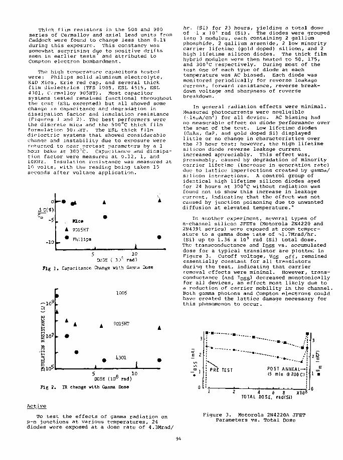
Thick film resistors in the 500 and 900series of Cermalloy and axial lead units fromCaddock were found to change less than 0.1%during this exposure. This constancy wassomewhat surprising due to positive driftsseen in earlier tests' and attributed toCorapton electron bombardment.
The high temperature capacitors testedwere: Philips solid aluminum electrolyte,K&D Mica, Erie red cap, and several thickfilm dielectrics (TFS 1005, ESL 4515, ESL4301, CVrmalloy 905HT). Most capacitorsystems tested remained functional throughoutthe test (ESL excepted) but all showed somechange in capacitance and degradation indissipation factor and insulation resistance(Figures 1 and 2). The best performers werethe discrete mica and the 500°C thick filmformulation 90.L-.HT. The ESL thick filmdielectric systems that showed considerablechange and instability due to exposure werereturned to near pretest parameters by a 1hour bake at 300'c. Capacitance and dissipa-tion factor were measured at 0.12, 1, and10KHz. Insulation resistance was measured at10 volts, with the reading being taken 15seconds after voltaqe application.
0 "--
A
> *
Klca
9315HT
Philips
A
*
A
1
A_C{%)
-10
5 c
DO3E ( 10 rad)
Fig 2. Caracitar.ee Change with Garar.a Dose
a
aio5
1005
9015hT
1301
5 „ ioDOSE (10° rad)
Fig 2. IR change with Gamma Dose
Active
To test the effects of gamma radiation onp-n junctions at various temperatures, 24diodes were exposed at a dose rate of 4.3Mrad/
hr. (Si) for 23 hours, yielding a total doseof -1 x 10' rad (Si) . The diodes were groupedinto 3 modules, each containing 2 galliumphosphide, 2 gallium arsenide, 2 low minoritycarrier lifetime (gold doped) silicon, and 2high lifetime silicon diodes. The thick filmhybrid modules were then heated to 50, 175,and 300°C respectively. During most of thetest one of each type of diode at eachtemperature was AC biased. Each diode wasmonitored periodically for reverse leakagecurrent, forward resistance, reverse break-down voltage and sharpness of reversebreakdown.
In general radiation effects were minimal.Measured photocurrents were negligible(• 16MA/CIII2) for all devics. AC biasing hadno measurable effect on diode performance overthe spar, of the test. Low lifetime diodes(GaAs, GaP, and gold doped Si) displayedlittle or no change in characteristics overthe 23 hour test; however, the high lifetimesilicon diode reverse leakage currentincreased appreciably. This effect was,presumably, caused by degradation of minoritycarrier lifetime (increase in generation rate)due to lattice imperfections created by gamma/silicon interactions. A control group ofidentical high lifetime silicon diodes agedfor 24 hours at 300°C without radiation wasfound not to show this increase in leakagecurrent, indicating that the effect was notcaused by junction poisoning due to unwanteddiffusion at elevated temperature.u
In another experiment, several types ofn-channel silicon JFETs (Motorola 2N4220 and2N4391 series) were exposed at room temper-ature to a gamma dose rate of ^1.7Mrad/hr.(Si) up to 1.36 x 10⁹ rad (Si) total dose.The transconductance and IDSS V S . accumulateddose for a typical transistor are plotted inFigure 3. Cutoff voltage, VGS off/ remainedessentially constant for all transistorsduring the test, indicating that carrierremoval effects were minimal. However, trans-conductance (and IDSS) decreased monotonicallyfor all devices, an effect most likely due toa reduction of carrier mobility in the channel.Both gamma photons and Compton electrons couldhave created the lattice damage necessary forthis phenomenon to occur.
f-.
' PRE TEST POST ANNEAL—I(5 min @200CI
2 A 6 S X108TOTAL DOSE, rad(Si)
Figure 3. Motorola 2N4220A JFETParameters vs. Total Dose
Jo
94
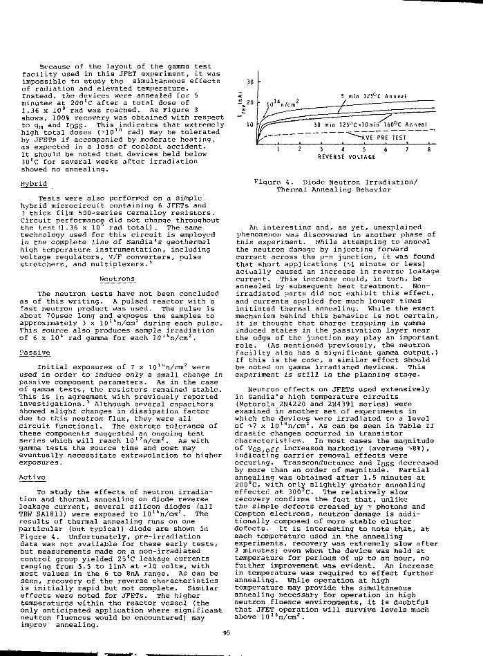
Because of the layout of the gamma testfacility used in this JFET experiment, it wasimpossible to study the simultaneous effectsof radiation and elevated temperature.Instead, the devices were annealed for 5minutes at 200°C after a total dose of1.36 x 109 rad was reached. As Figure 3shows, 100% recovery was obtained with respectto gm and IDSS- This indicates that extremelyhigh total doses (>1O10 rad) may be toleratedby JFETs if accompanied by moderate heating,as expected in a loss of coolant accident.It should be noted that devices held below30'c for several weeks after irradiationshowed no annealing.
Tests were also performed on a simplehybrid microcircuit containing 6 JFETs and3 thick film 500-series Cermalloy resistors.Circuit performance did not change throughoutthe test (1.36 x 10" rad total). The sametechnology used for this circuit is employedin the complete line of Sandia's geothermalhigh temperature instrumentation, includingvoltage regulators, V/F converters, pulsestretchers, and multiplexers.5
Neutrons
The neutron tests have not been concludedas of this writing. A pulsed reactor with afast neutron product was used. The pulse isabout 70psec long and exposes the samples toapproximately 3 x lO^n/cm2 during each pulse.This source also produces sample irradiationof 6 x 10' rad gamma for each 10J1>n/cm2.
Passive
Initial exposures of 7 x 101'*n/cm2 wereused in order to induce only a small change inpassive component parameters. As in the caseof gamma tests, the resistors remained stable.This is in agreement with previously reportedinvestigations.3 Although several capacitorsshowed slight changes in dissipation factordue to this neutron flux, they were allcircuit functional. The extreme tolerance ofthese components suggested an ongoing testseries which will reach 10I7n/cm . As withgamma tests the source time and cost mayeventually necessitate extrapolation to higherexposures.
Active
To study the effects of neutron irradia-tion and thermal annealing on diode reverseleakage current, several silicon diodes {allTRW SA1813) were exposed to 10ll*n/cm2. Theresults of thermal annealing runs on oneparticular (but typical) diode are shown inFigure 4. Unfortunately, pre-irradiationdata was not available for these early tests,but measurements made on a non-irradiatedcontrol group yielded 25°C leakage currentsranging from 5.5 to llnA at -10 volts, withmost values in the 6 to 8nA range. As can beseen, recovery of the reverse characteristicsis initially rapid but not complete. Similareffects were noted for JFETs. The highertemperatures within the reactor vessel (theonly anticipated application where significantneutron fluences would be encountered) mayimprov annealing.
30
•5 20
10
5 m i n ! 2 5 ° C A n n e a l
30 m i n 1 2 5 ° C +10miiii 1 6 0 ° C A n n e a l
~"~"-AVE PRE TEST
1 2 3 4 5 6REVERSE VOLTAGE
Figure 4. Diode Neutron Irradiation/Thermal Annealing Behavior
An interesting and, as yet, unexplainedphenomenon was discovered in another phase ofthis experiment. While attempting to ann&althe neutron damage by injecting forwardcurrent across the p-n junction, it was foundthat short applications ( 1 minute or less)actually caused an increase in reverse leakagecurrent. This increase could, in turn, beannealed by subsequent heat treatment. Non-irradiated parts did not exhibit this effect,and currents applied for much longer timesinitiated thermal annealing. While the exactmechanism behind this behavior is not certain,it is thought that charge trapping in gammainduced states in the passivation layer nearthe edge of the junction may play an importantrole. (As mentioned previously, the neutronfacility also has a significant gamma output.)If this is the case, a similar effect shouldbe noted on gamma irradiated devices. Thisexperiment is still in the planning stage.
Neutron effects on JFETs used extensivelyin Sandia's high temperature circuits(Motorola 2N4220 and 2N4391 series) wereexamined in another set of experiments inwhich the devices were irradiated to a levelof ^7 x 10l*n/cm2. As can be seen in Table IIdrastic changes occurred in transistorcharacteristics. In most cases the magnitudeof VGs,off increased markedly (average ^ 8 % ) ,indicating carrier removal effects wereoccuring. Transconductance and IDSS decreasedby more than an order of magnitude. Partialannealing was obtained after 1.5 minutes at200°C, with only slightly greater annealingeffected at SOO^C. The relatively slowrecovery confirms the fact that, unlikethe simple defects created by y photons andCompton electrons, neutron^damage is addi-tionally composed of more stable clusterdefects. It is interesting to note that, ateach temperature used in the annealingexperiments, recovery was extremely slow after2 minutes; even when the device was held attemperature for periods of up to an hour, nofuLther improvement was evident. An increasein temperature was required to effect furtherannealing. While operation at hightemperature may provide the simultaneousannealing necessary for operation in highneutron fluence environments, it is doubtfulthat JFET operation will survive levels muchabove 1016n/cm2.
95
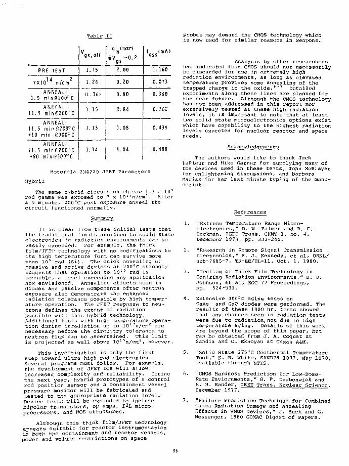
Table II
PRE TEST
7 X 1 0 1 4 n / c m 2
ANNEAL:1.5 min@200°C
ANNEAL:11.5 min@200 cC
ANNEAL:11.5 min@200°C+ 10 min @300°C
ANNEAL:11.5 min<?'200°C+80 min@300°C
V g s , o f f
1.15
1.24
(1 .36 )
1.15
1. 13
1.14
@V-0.22.00
0 .20
0 .80
0 .84
1.08
1.04
l d s s < m A )
1.160
0.073
0.360
0.362
0.439
0.488
Motorola 2N4220 JFET Parameters
The same hybrid circuit which saw 1.3 x 10°rad gamma was exposed to 7 x lO'''n/cm2 . Aftera 5 minute, 200°C post exposure anneal thecircuit functioned normally.
Summary
It is clear from these initial tests thatthe traditional limits ascribed to solid stateelectronics in radiation environments can bevastly exceeded. For example, the thickfilm/JFET technology with no modifications toits high temperature form can survive morethan 10' rad (Si). The quick annealing ofpassive and active devices at 200°C stronglysuggests that operation to 1010 rad ispossible, a level exceeding any applicationnow envisioned. Annealing effects seen indiodes and passive components after neutronexposure also demonstrate the enhancedradiation tolerance possible by high temper-ature operation. The JFET response to neu-trons defines the extent of radiationpossible with this hybrid technology.Additional tests with high temperature^opera-tion during irradiation up to 10I7n/cm2 arenecessary before the circuitry tolerance toneutron flux can be ascertained. This limitis projected as well above 1015n/cm2, however.
This investigation is only the firststep toward ultra high rad electronics.Several programs must follow. For example,the development of JFET ICs will allowincreased complexity and reliability. Duringthe next year, hybrid prototypes of a controlrod position sensor and a containment vesselpressure monitor will be fabricated andtested to the appropriate radiation level.Device tests will be expanded to includebipolar transistors, op amps, I2L micro-processors, and MOS structures.
Although this thick film/JFET technologyappears suitable for reactor instrumentationin both the containment and reactor vessels,power and volume restrictions on space
probes may demand the CMOS technology whichis now used for similar reasons in weapons.
Analysis by other researchershas indicated that CMOS should not necessarilybe discarded for use in extremely highradiation environments, as long as elevatedtemperature provides some annealing of thetrapped charge in the oxide.6'7 Detailedexperiments along these lines are planned forthe near future. Although the CMOS technologyhas not been addressed in this report norextensively tested at these high radiationlevels, it is important to note that at leasttwo solid state microelectronics options existwhich have capability to the highest radiationlevels expected for nuclear reactor and spaceneeds.
Acknowledgements
The authors would like to thank JackLaFleur and Mike Garner for supplying many ofthe devices used in these tests, John McBiayerfor enlightening discussions, and BarbaraMacias for her last minute typj.ng of the manu-script.
References
1. "Extreme Temperature Range Micro-electronics," D. W. Palmer and R. C.Heckman, IEEE Trans. CHMT-1, No. 4,December 1973, pp. 333-340.
2. "Research in Remote Signal TransmissionElectronics," E. J. Kennedy, et al, ORNL/sub-7685-7, TR-EE/EL-11, Oct. 1, 1980.
3. "Testing of Thick Film Technology inIonizing Radiation Environments," D. R.Johnson, et al, ECC 77 Proceedings,pp. 524-531.
4. Extensive 300°C aging tests onGaAs and GaP diodes were performed. Theresults of these 1000 hr. tests showedthat any changes seen in radiation testswere due to radiation, not due to hightemperature aging. Details of this workare beyond the scope of this paper, butcan be obtained from J. A. Coquat atSandia and O. Eknoyan at Texas ASM.
5. "Solid State 275°C Geothermal TemperatureTool," K. R- White, SAND78-1037, May 1978,available through NTIS.
6. "CMOS Hardness Prediction for Low-Dose-Rate Enviornments," G. F. Derbenwick andH. H. Sander, IEEE Trans. Nuclear Science,December 1977. ' "
7. "Failure Prediction Technique for CombinedGamma Radiation Damage and AnnealingEffects in VMOS Devices," J. Buck and G.Messenger, 1980 GOMAC Digest of Papers.
96
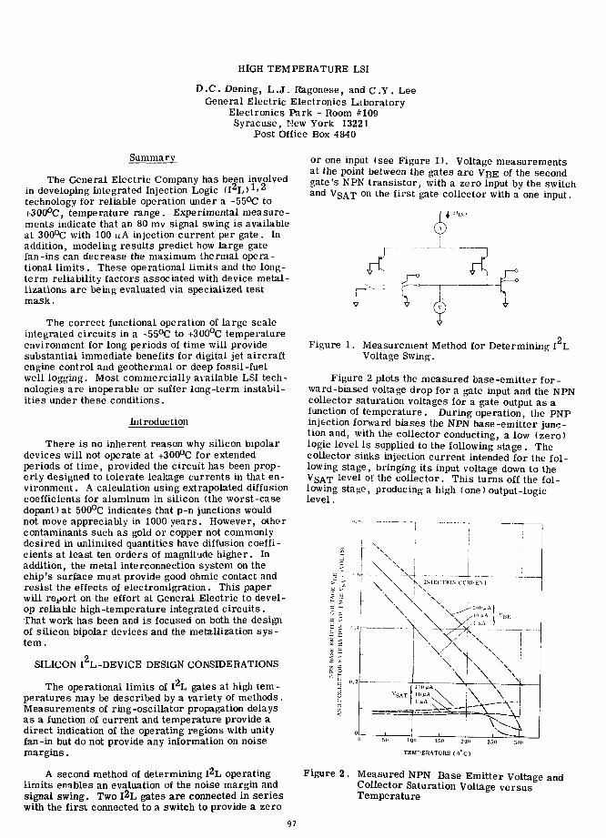
HIGH TEMPERATURE LSI
D.C. Dening, L.J. Ragonese, and C .Y. LeeGeneral Electric Electronics Laboratory
Electronics Park - Room *109Syracuse, New York 13221
Post Office Box 4840
Summary
The General Electric Company has been involvedin developing Integrated Injection Logic <I*L>*>'*technology for reliable operation under a -55°C to+300°C, temperature range . Experimental measure-ments indicate that an 80 mv signal swing is availableat 300°C with 100 jiA injection current per gate. Inaddition, modeling results predict how large gatefan-ins can decrease the maximum thermal opera-tional limits . These operational limits and the long-term reliability factors associated with device metal-lizations are being evaluated via specialized testmask.
The correct functional operation of large scaleintegrated circuits in a -55°C to +300°C temperatureenvironment for long periods of time will providesubstantial immediate benefits for digital jet aircraftengine control and geothermal or deep fossil-fuelwell logging. Most commercially available LSI tech-nologies are inoperable or suffer long-term instabil-ities under these conditions.
Introduction
There is no inherent reason why silicon bipolardevices will not operate at +300°C for extendedperiods of time, provided the circuit has been prop-erly designed to tolerate leakage currents in that en-vironment . A calculation using extrapolated diffusioncoefficients for aluminum in silicon (the worst-casedopant) at 500°C indicates that p-n junctions wouldnot move appreciably in 1000 years. However, othercontaminants such as gold or copper not commonlydesired in unlimited quantities have diffusion coeffi-cients at least ten orders of magnitude higher. Inaddition, the metal interconnection system on thechip's surface must provide good ohmic contact andresist the effects of electromigration. This paperwill report on the effort at General Electric to devel-op reliable high-temperature integrated circuits.That work has been and is focused on both the designof silicon bipolar devices and the metallization sys-tem .
SILICON I2L -DEVICE DESIGN CONSIDERATIONS
The operational limits of I^L gates at high tem-peratures may be described by a variety of methods .Measurements of ring-oscillator propagation delaysas a function of current and temperature provide adirect indication of the operating regions with unityfan-in but do not provide any information on noisemargins.
A second method of determining I^L operatinglimits enables an evaluation of the noise margin andsignal swing. Two I2L gates are connected in serieswith the first connected to a switch to provide a zero
o r o n e in p u t ( s e e figure 1). Voltage measurementsat the point between the gates are VRE of the second,,a t e . s N P N transistor, with a zero input by the switcha n d V g A T on t h e f i r s t mte c o i l e c t o r w i t h a o n e i n p u t
Figure 1. Measurement Method for Determining I LVoltage Swing.
Figure 2 plots the measured base-emitter for-ward-biased voltage drop for a gate input and the NPNcollector saturation voltages for a gate output as afunction of temperature. During operation, the PNPinjection forward biases the NPN base-emitter junc-tion and, with the collector conducting, a low (zero)logic level is supplied to the following stage. Thecollector sinks injection current intended for the fol-lowing stage, bringing its input voltage down to theVSAT level of the collector. This turns off the fol-lowing stage, producing a high (one) output-logiclevel.
H
150 2011 250
TEMPERATURE < o " c >
Figure 2 . Measured NPN Base Emitter Voltage andCollector Saturation Voltage versusTemperature
97
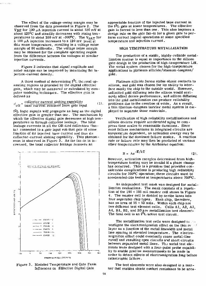
The effect of the voltage-swing margin may beobserved from the data presented in Figure 2 . TheVBE for 100 /iA injection current is about 550 mV atabout 125°C and steadily decreases with rising tem-peratures to about 200 mV at +300°C. The VgAT f o r
a 100 A injection increases to a 120 mV level atthis same temperature, resulting in a voltage noisemargin of 80 millivolts. The voltage noise marginmay be obtained for the complete operating regionfrom the difference between the voltages at similarinjection currents.
Figure 2 indicates that signal amplitude andnoise margin can be improved by increasing the in-jection-current density.
A third method of determining I2L thermal op-erating regions is provided by the digital effectivegain, which may be measured or calculated by com-puter modeling techniques. The effective gfiin isdefined as
peff:collector current sinking capabilitybase current removed from gate input (1).
I L logic signals will propagate as long as the digitaleffective gain is greater than one. The mechanism bywhich the effective digital gain decreases at high tem-peratures is through collector leakage. The totalleakage currents in all the OB-tied collectors (fan-in) connected to a gate input rob that gate of somefraction of its injected base current and thus itscollector-current sinking capability. This phenom-enon is observed in Figure 3. As the fan-in is in-creased, the total collector leakage removes an
Vt
F
p
VN1N
KStS
\NIN
VNIN
VNIN
VMS
" -
•i
i;
B
- l l
,11111
liI I I
-51) 0 101 l">0 200
TEMPEIiATUHE ( CELSIUS}
Figure 3. Modeled Temperature and Gate FaninInfluences on Effective Digital Gain
appreciable fraction of the injected base current inthe l^L gate at lower temperatures. The effectivegain is forced to less than one. This also imposes adesign rule on the gate fan-in for a given gate to per-form correct logical operations at some specifiedtemperature and injection current.
HIGH TEMPERATURE METALLIZATION
The production of a stable, highly-reliable metal-lization system is equal in importance to the silicongate design in the production of high-temperature LSI.The metal system chosen for the high-temperatureapplications is platinum silicide/titanium-tungsten/gold.
Platinum silicide forms stable ohmic contacts tosilicon, and gold was chosen for its ability to inter-face easily the chip to the outside world. However,unlimited gold diffusing into the silicon would seri-ously affect device performance, and silicon diffusinginto the gold metallization can produce reliabilityproblems due to the creation of voids. As a result,a thin titanium-tungsten barrier metal system is em-ployed to separate those materials.
Verification of high reliability metallizations andsilicon devices require accelerated aging to com-press time scales to reasonable durations. Sincemost failure mechanisms in integrated circuits aretemperature dependent, an activation energy may beobtained for the dominant failure modes. A reactionrate or failure rate may then be predicted at variousother temperatures by the Arrhenius equation:
R = Ae-E/kT
( 2 ) .
However, activation energies determined from high-temperature testing may be invalid if a phase changehas occurred. This is a problem that provides con-siderable complications in producing high reliabilitycircuits for 300°C operation; these circuits must beaccelerated -life tested at temperatures above 350°C.
An independent test mask was designed for metal-lization evaluations. The mask consists of a repeti -tion of the 190 x 186 mil master cell shown in Figure4. The master cell is divided by scribe lanes intofour separable chip types. Each chip, therefore,has an area of 95 x 93 mils. Within each chip aretwo different test element cells. Cells Al, A2, A3,A4, Bl, B2, and B3are metallization test elementsThe final cell is an I2L active test circuit.
The metallization test cells were designed tovestigate the electromigration effect on the thin m: ;
layer as a function of the metal linewidth and metalline spacing at elevated temperature. The electro-migration effect could eventually cause metal-linerunoff and resulting open circuits and short circuitsbetween separated metal lines. Thj metal test ele-ments were designed with a four-point probe capabil-ity to enable precise measurements to be made inorder to detect effects of electromigration long beforecatastrophic failure.
The test elements were also designed in a man-ner that enables ohmic contact resistance to be accu-
98
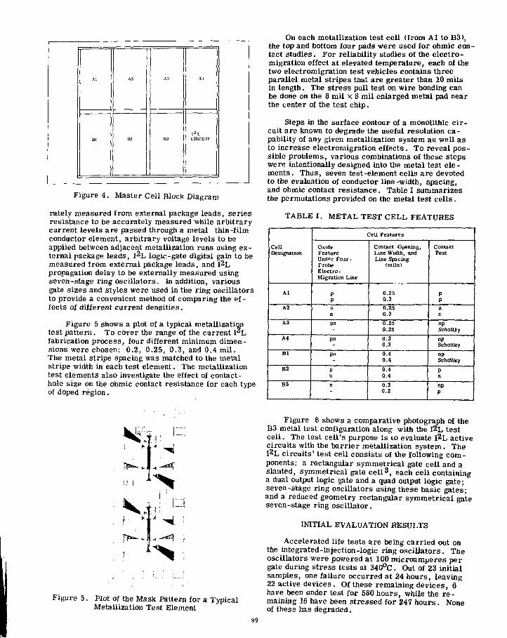
Figure 4. Master Cell Block Diagram
rately measured from external package leads, seriesresistance to be accurately measured while arbitrarycurrent levels are passed through a metal thin-filmconductor element, arbitrary voltage levels to beapplied between adjacent metallization runs using ex-ternal package leads, ]2L logic-gate digital gain to bemeasured from external package leads, and I^Lpropagation delay to be externally measured usingseven-stage ring oscillators. In addition, variousgate sizes and styles were used in the ring oscillatorsto provide a convenient method of comparing the ef-fects of different current densities.
Figure 5 shows a plot of a typical metallizationtest pattern. To cover the range of the current l^Lfabrication process, four different minimum dimen-sions were chosen: 0.2, 0.25, 0.3, and 0.4 mil.The metal stripe spacing was matched to the metalstripe width in each test element. The metallizationtest elements also investigate the effect of contact-hole size on the ohtnic contact resistance for each typeof doped region.
On each metallization test cell (from Al to B3),the top and bottom four pads were used for ohmic con-tact studies. For reliability studies of the electro-migration effect at elevated temperature, each of thetwo electromigration test vehicles contains threeparallel metal stripes that are greater than 10 milsin length. The stress pull test on wire bonding canbe done on the 8 mil x 8 mil enlarged metal pad nearthe center of the test chip.
Steps in the surface contour of a monolithic cir-cuit are known to degrade the useful resolution ca-pability of any given metallization system as well asto increase electromigration effects. To reveal pos-sible problems, various combinations of these stepswere intentionally designed into the metal test ele-ments. Thus, seven test-element cells are devotedto the evaluation of conductor line-width, spacing,and ohmic contact resistance. Table I summarizesthe permutations provided on the metal test cells.
TABLE I. METAL TEST CELL FEATURES
CellDesignation
Al
A2
A3
A4
Bl
B2
B3
Cell Features
OxideFeatureUnd**r Four-FrobeElectro-Migration Line
PPnn
pn
pn
Pn
Pn
n
Contact Opening,Line Width, andLine Spacing
(mils)
0.250.3
0.250.3
0.250.25
0.30.3
0.40.4
0.40.4
0.20.2
ContactTest
PPnn
npSchottky
npSchottky
npSchottky
Pn
npP
V.: C
i . >•
Figure 5. Plot of the Mask Pattern for a TypicalMetallization Test Element
Figure 6 shows a comparative photograph of theB3 metal test configuration along with the I2L testcell. The test cell's purpose is 10 evaluate I2L activecircuits with the barrier metallization system. TheI2L circuits' test cell consists of the following com-ponents: a rectangular symmetrical gate cell and aslanted, symmetrical gate cell3, each cell containinga dual output logic gate and a quad output logic gate;seven-stage ring oscillators using these basic gates;and a reduced geometry rectangular symmetrical gateseven-stage ring oscillator.
INITIAL EVALUATION RESULTS
Accelerated life tests are being carried out onthe integrated-injection-logic ring oscillators. Theoscillators were powered at 100 microamperes pergate during stress tests at 340°C. Out of 23 initialsamples, one failure occurred at 24 hours, leaving22 active devices. Of these remaining devices, 6have been under test for 580 hours, while the re-maining 16 have been stressed for 247 hours. Noneof these has degraded.
99
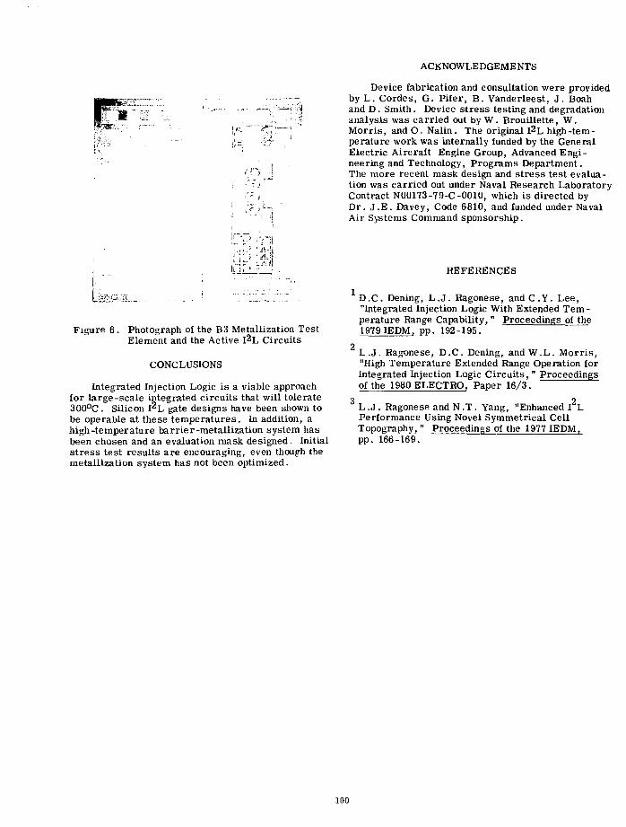
] . < - . '
" " • " * -
ACKNOWLEDGEMENTS
Device fabrication and consultation were providedby L. Cordes, G. Pifer, B. Vanderleest, J . Boahand D. Smith. Device stress testing and degradationanalysis was carried out by W . Brouillette, W.Morris, and O. Nalin. The original I^L high-tem-perature work was internally funded by the GeneralElectric Aircraft Engine Group, Advanced Engi-neering and Technology, Programs Department.The more recent mask design and stress test evalua-tion was carried out under Naval Research LaboratoryContract N00173-79-C-0010, which is directed byDr. J . E . Davey, Code 6810, and funded under NavalAir Systems Command sponsorship.
REFERENCES
Figure 6. Photograph of the B3 Metallization TestElement and the Active I2L Circuits
CONCLUSIONS
Integrated Injection Logic is a viable approachfor large-scale integrated circuits that will tolerate300°C. Silicon I^L gate designs have been shown tobe operable at these temperatures. In addition, ahigh-temperature barrier-metallization system hasbeen chosen and an evaluation mask designed. Initials t ress test results are encouraging, even though themetallization system has not been optimized.
D.C. Dening, L . J . Ragonese, andC.Y. Lee,"Integrated Injection Logic With Extended Tem-perature Range Capability, " Proceedings of the1979 IEDM, pp. 192-195.
2L . J . Ragonese, D.C. Dening, andW.L . Morris ,"High Temperature Extended Range Operation forIntegrated Injection Logic Circuits, " Proceedingsof the 1980 ELECTRO, Paper 16/3.
3 2L . J . Ragonese and N.T . Yang, "Enhanced I LPerformance Using Novel Symmetrical CellTopography, " Proceedings of the 1977 IEDM,pp. 166-169.
100
SAND81-0345CHIGH-TEMPERATURE COMPLEMENTARY METAL
OXIDE SEMICONDUCTORS (CMOS)
John D. McBrayerDivision 2117
Sandia National LaboratoriesAlbuquerque, New Mexico 87185
Introduction
The theory on which silicon (Si) metaloxide semiconductors (MOS) technology isfounded states that this type semiconductorwill perform adequately at 300°C. Hightemperature tests conducted on commerciallyavailable MOS field effect transistors (FET)have confirmed this hypothesis.'"3 In thisreport, we present the results of an inves-tigation into the possibility of using CMOStechnology at Sandia National Laboratories(SNLA) for high temperature electronics. ACMOS test chip (TO was specifically developedas the test bed. This test chip incorporatesCMOS transistors that have no gate protectiondiodes; these diodes are the major cause ofleakage in commercial devices.
We decided to use CMOS technology becauseboth n- and p-channel devices could be eval-uated. We also looked at small-scale inte-tration, e.g., an inverter using CMOS junctionisolation and a simulation of dielectricisolation.
Theory and actual data have been comparedbefore.3 In this paper we intend to reporton the aging and stability of CMOS devices;especially where requirements call for minimaldrift when subjected to 300°C for 1000 hours.This drift must be less than that in devicestaken from room temperature to 300°C.
Fr^ I semiconductor physics, the followinggeneralization can be made:
• As temperature increases, theFermi level moves toward the middleof the band gap, causing the built-in potential to decrease, therebydecreasing the threshold voltage.
• As temperature increases, the bandgap narrows, causing a minor increasein the intrinsic carrier concen-tration,
• Carrier mobility decreases withincreasing temperature, causingtransconductance to decrease.
• Increasing temperature Increasesleakage of generated and diffusedcurrents.
• The more the doping, the greaterthe variation in threshold voltageas temperature increases.
• The zero temperature coefficientpoint occurs at higher gatevoltages as the doping is increased.
• The overall transconductance decreasesrapidly as temperature and dopinqincreases.
With these generalizations in mind, we madethe process variation listed in Table 1.
Table 1
.B - 1 . ? -r-T n lvp»
- ^ixlD 1 ' ' r ir" 3
. B - 1. ?f en n- ; yp*1
1 ci - 3
NS ^ ixir. -
r«ro r. fin k..v >.:
These variations are adjustments of thevarious doping levels that compose the MOSFETs,and they require many trade-offs in electricalperformance, making optimization difficult(Tables 2 and 3). Table 2 shows that,although wafer 1 produces symmetrical gatevoltages, leakage and transconductance varygreatly between the two channels. Wafer 9performs well in leakage and voltage but notin transconductance.
All wafers except No. 5 performed aspredicted by theory. The anomaly of wafer 5remains unexplained. The tables show theaverage values derived after subjecting thewafers to 300°C for 1000 hours. Thresholdvoltages for the surviving devices are within±0.1V of those listed in Tables 2 and 3;leakages are within ±5JJA of those listed inTable 2, and 25/JA of those in Table 3.According to theory, the following patternshould appear.
For wafers 1 and 5, p-channel data shouldbe similar.
For wafers 7 and 9, p-channel data shouldbe similar.
For wafers 5 and 7, n-channel data shouldbe similar.
101
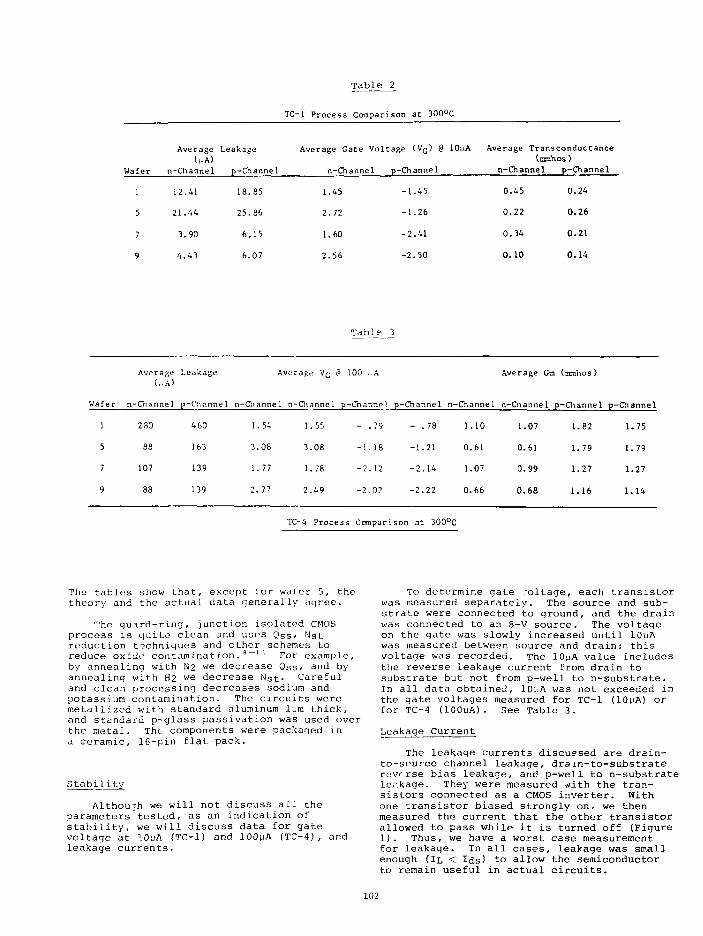
Table 2
TC-1 Process Comparison at 300°C
Average Leakage(,-A)
Wafer n-Channel p-Channel
Average Gate Voltage (VQ) @ lOuA Average Transconductance(cmhos )
n-Channel p-Channel n-Channel p-Channel
1
5
7
9
12
21
3
4
.41
.44
.90
.43
18
25
6
6
.85
.86
.15
.07
1
2
1
2
.45
.72
.60
.56
-1
-1
-2
-2
.45
.26
.41
.50
0.
0.
0.
0.
45
22
34
10
0.
0.
0.
0.
24
26
21
14
Table 3
Average Leakage Average \'Q & 100 ..A Average Gm (ncnhos)
Wafer n-C'nanne 1 p-Channe I n-Channe 1 n-Diannel p-Cnanne1. p-Channel n-Channel n-Channel p-Channel p-Channel
2 80
107
83
4 60
163
139
139
1.54
3.08
1.77
2.77
1.55
3.08
1.78
2.49
.79
1.18
2.12
2.02
- .
-1.
-2.
-2.
78
21
14
22
1.
0.
1.
0.
10
61
07
66
1.
0.
0.
0.
07
61
99
68
1.
1.
1.
1.
82
79
27
16
1.
1.
1.
1.
75
79
27
14
TC-4 Process Comparison at 300°C
The tables show that, except for wafer 5, thetheory and the actual data qenerally aqree.
The quird-rinq, junction isolated CMOSprocess is quite clean and uses Qss/ Nstreduction techniques and other schemes toreduce oxide contamination.8"11 For example,by annealinq with N2 we decrease Qss, and byannealing with H2 w e decrease Nst- Carefuland clean processing decreases sodium andpotassium contamination. The circuits weremetallized with standard aluminum lum thick,and standard p~glass passivation was used overthe metal. The- components were packaged ina ceramic, 16-pin flat pack.
Stability
Althoujh we will not discuss all theparameters tested, as an indication ofstability, we will discuss data for gatevoltage at \0uA (TC-1) and 100MA (TC-4), andleakage currents.
To determine gate -oltage, each transistorwas measured separately. The source and sub-strate were connected to ground, and the drainwas connected to an 8-V source. The voltageon the gate was slowly increased until lOuAwas measured between source and drain; thisvoltage was recorded. The 10uA value includesthe reverse leakage current from drain tosubstrate but not from p-well to n-substrate.In all data obtained, IOJIA was not exceeded inthe gate voltages measured for TC-1 (10pA) orfor TC-4 (lOOuA). See Table 3.
Leakage Current
The leakage currents discussed are drain-to-source channel leakage, drain-to-substratereverse bias leakage, and p-well to n-substrateler.kage. They were measured rfith the tran-sistors connected as a CMOS inverter. Withone transistor biased strongly on. we thenmeasured the current that the othtir transistorallowed to pass whilf* it is turned off (Figure1) . Thus, we have a worst case measurementfor leakage. In all cases, leakage was smallenough (II < Ids) to allow the semiconductorto remain useful in actual circuits.
102
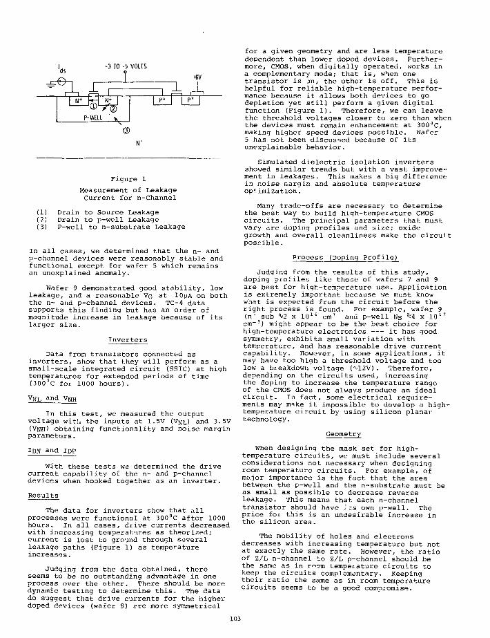
ds
P-WEU y
Figure 1
Measurement of LeakageCurrent for n-Channel
(1) Drain to Source Leakage(2) Drain to p-well Leakage(3) P-well to n-substrate Leakage
In all cases, we determined that the n- andp-channel devices were reasonably stable andfunctional except for wafer 5 which remainsan unexplained anomaly.
Wafer 9 demonstrated good stability, lowleakage, and a reasonable V G at lOyiA on boththe n- and p-channel devices. TC-4 datasupports this finding but has an order ofmagnitude increase in leakage because of itslarger size.
Inverters
Data from transistors connected asinverters, show that they will perform as asmall-scale integrated circuit (SSIC) at hightemperatures for extended periods of time(300 C for 1000 hours).
and V N H
In this test, we measured the outputvoltage witl. the inputs at 1.5V (VJJL) and 3.5V(V N H ) obtaining functionality and noise marginparameters.
IDN and I D P
With these tests we determined the drivecurrent capability of the n- and p-channeldevices when hooked together as an inverter.
Results
The data for inverters show that allprocesses were functional at 300°C after 1000hours. In all cases, drive currents decreasedwith increasing temperatures as theorized;current is lost to ground through severalleakage paths (Figure 1) as temperatureincreases.
Judging from the data obtained, thereseems to be no outstanding advantage in oneprocess over the other. There should be moredynamic testing to determine this. The datado suggest that drive currents for the higherdoped devices (wafer 9) ere more symmetrical
for a given geometry and are less temperaturedependent than lower doped devices. Further-more, CMOS, when digitally operated, works ina complementary mode; that is, when onetransistor is _>n, the other is off. This ishelpful for reliable high-temperature perfor-mance because it allows both devices to godepletion yet still perform a given digitalfunction (Figure 1 ) . Therefore, we can leavethe threshold voltages closer to zero than whenthe devices must remain enhancement at 300°C,making higher speed devices possible. Wafer5 has not been discussed because of itsunexplainable behavior.
Simulated dielectric isolation invertersshowed similar trends but with a vast improve-ment in leakages. This makes a big differencein noise n.argin and absolute temperatureoptimization.
Many trade-offs are necessary to determinethe best way to build high-temperature CMOScircuits. The principal parameters that mustvary are doping profiles and size; oxidegrowth and overall cleanliness make the circuitpossible.
Process (Doping Profile)
Judging from the results of this study,doping profiles like those of wafers 7 and 9are best for high-temperature use. Applicationis extremely important because we must knowwhat is expected from the circuit before theright process is found. For example, wafer 9
1 6 % 7(n- sub %2 x 10 1 and p-well Ns % 4 x 10 1
an"3) might appear to be the best choice forhigh-temperature electronics it has goodsymmetry, exhibits small variation withtemperature, and has reasonable drive currentcapability. However, in some applications, itmay have too high a threshold voltage and toolow a breakdown voltage (^12V). Therefore,depending on the circuits used, increasingthe doping to increase the temperature rangeof the CMOS does not always produce an idealcircuit. In fact, some electrical require-ments may m=ike it impossible to develop a high-temperature circuit by using silicon planartechnology.
Geometry
When designing the mask set for high-temperature circuits, we must include severalconsiderations not necessary when designingroom temperature circuits. For example, ofmajor importance is the fact that the areabetween the p-well and the n-substrate must beas small as possible to decrease reverseleakage. This means that each n-char.neltransistor should have S is own p-well. Theprice for this is an undesirable increase inthe silicon area.
The mobility of holes and electronsdecreases with increasing temperature but notat exactly the same rate. However, the ratioof z/L n-channel to Z/L p-channel should bethe same as in r<~>om temperature circuits tokeep the circuits complementary. Keepingtheir ratio the same as in room temperaturecircuits seems to be a good compromise.
103
For high temperature circuits, the area Surfaces," IEEE Transactions Electronfrom the drain to the substrate junction Devices, 248, May 1965.should be as small as possible to decreasereverse leakage. This is accomplished by 9. F. N. Schrieffer, Effective Carrierhorseshoeing the Z/Ls, thereby increasing Mobility in Surface-Space Chargecircuit density — this method is already in Layers," Phys. Review, 97, pp. 641,common use. 1955.
To make high-temperature circuits more 10. W. M. Bullis, "Properties of Gold inreliable, metal lines should be as broad and Silicon," Solid-state Electronics, 9deep as possible, again sacrificing chip area. pp. 143, 1966.
Conclusions 11. B. E. Deal, et al., "Characteristicsof the Surface State Charge (Qss) of
Existing CMOS technology can be used to Thermally Oxidized Silicon,"produce stable and useful circuits that oper- Electrochemical Society, 144, pp. 266,ate at 300°C for 1000 hours. This accomplish- 1967.ment, however, sacrifices some chip area anddoes not provide gate protection. For this 12. C. W. White, J. Narayans, and R. T.latter problem, high-temperature GaAs and Young, "Laser Annealing of Ion-Gap diodes should be developed as protection Implanted Semiconductors," Science,devices. Although these diodes would probably 204 (4382) :461, May 1979.be outside the CMOS chip, they could be partof the same flat pack. 13. J. D. McBrayer, "High-Temperature
Complementary Metal Oxide Semicon-Dielectric isolation CMOS would be a ductors (CMOS)," Sandia National
great improvement over junction isolation and Laboratories, SAND79-1487, Octoberwork has begun in this area. New solar cell 1979.diodes show promise as input protectiondevices. This would allow us to be completelyintegrated again.
References
1. J. L. Prince of Clemson University,Investigation of the Performance ofSemiconductor Devices at ElevatedTemperatures, Sandia NationalLaboratories, under Contract No.06-4336, November 1977.
2. D. W. Palmer, B. L. Draper, J. D.McBrayer, and K. R. White, "ActiveDevices for High-TemperatureMicrocircuitry," Sandia NationalLaboratories, SAND77-114 5, February1978.
3. B. L. Draper and D. W. Palmer,"Extension of High-TemperatureElectronics," Proceedings of ECC,1979.
4. J. D. McBrayer, "CMOS Test Chips,"Sandia National Laboratories,SAND78-1390, August 1978.
5. A. S. Grove, Physics and Technologyof Semiconductor Devices, (New York,John Wiley & Sons, Inc.,) 1967.
6. S. M. Sze, Physics of SemiconductorDevices, (New York, Wiley-Interscience)1969.
7. W. M.-Penney and L. Lau, MOSIntegrated Circuits, (New York,Van Nostrand Reinhold Co.) 1972.
0. Leistiko, Jr., A. S. Grove,and C. T. Sah, "Electron andHole Mobilities in Inversion Layerson Thermally Oxidized Silicon
104
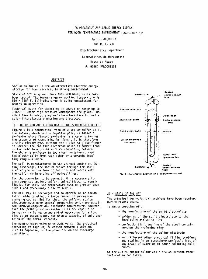
"A PRESENTLY AVAILABLE ENERGY SUPPLY
FOR HIGH TEMPERATURE ENVIRONMENT (G5O-10O00 F)"
by J. JACQUELIN
and R. L. VIC
Electrochemistry Department
Laboratoires de Marcoussis
Route de Nozay
F. 91460 MARCOUSSIS
ABSTRACT
Sodium-sulfur cells are an attractive electric energystorage for long service, in strong environment.
State of art is given. More than 200 Wh/kg cells havebeen tested. The known range of working temperature is550 - 750° F. Self-discharge is quite nonexistent formonths in operation.
Technical basis for expecting an operating range up to1 000° F under high pressure atmosphere are given. Pos-sibilities to adapt sizt and characteristics to parti-cular interplanetary mission are discussed.
1) - OPERATION AND TECHNOLOGY OF THE SODIUM-SULFUR CELL
Figure 1 is a schematical view of a sodium-sulfur cell.The sodium, which is the negative pole, is inside aB-alumina glove finger. B-alumina is a ceramic havingthe property of transiting Na+ ions ; it is thereforea solid electrolyte. Outside the g-alumina glove fingeris located the positive electrode which is formed fromsulfur held in a graphite-fibre conducting network.The whole is enclosed in two sts.el containers, sepated electrically from each other by a ceramic insulting ring a-alumina.
The cell is manufactured in the charged condition. Du-ring discharge, the sodium passes through the solidelectrolyte in the form of Na+ ions and reacts withthe sulfur while giving off polysulfides.
For the operation to be correct, 't is necessary forthe reagents, sodium, sulfur, polysulfides, to remainliquid. For that, the temperature must be greater than500° F and preferably close to 650° C.
The cell may be recharged and so operate as an accumu-lator, able to effect a large number of successivecharging cycles. But for that, the sulfur-graphiteelectrode must have special properties which are obtai-ned through complex ai,a elaborate manufacture. However,even the primary sodium-sulfur cells are capable ofbeing partially recharged and of operating for a longtime as an accumulator, but with a capacity of onlj one-third of the normal capacity.
The open-circuit voltage is 2.08 volts. The practicaloperating voltage is-ay be chosen between 1 volt and2 volts depending on the power and on the dischargeconditions.
Terminal —Sealedunder vacuumtube
Glass seal
Alpha-aluminaring
Sulfur electrodecontainer
Sulfur andgraphite felt
. SealedTerminal
tube
Fig. 1 : Schematic section ol a sodlum-lulfur call
l) - STATE OF THE ARTThe principal technological problems have been resolvedduring recent years.It was a question of :
- the manufacture of the solid electrolyte
- soldering of the solid electrolyte to theinsulating a-alumina ring
- perfectly tight sealing of the steel contai-ners on the a-alumina ring
- the manufacture of the sulfur electrode
- and different other practical filling problemsand sealing in an atmosphere perfectly free ofany trace of water or of other polluting mole-cules.
At the L.d.M. sodium-sulfur cells are at present manu-factured in two sizes.
107
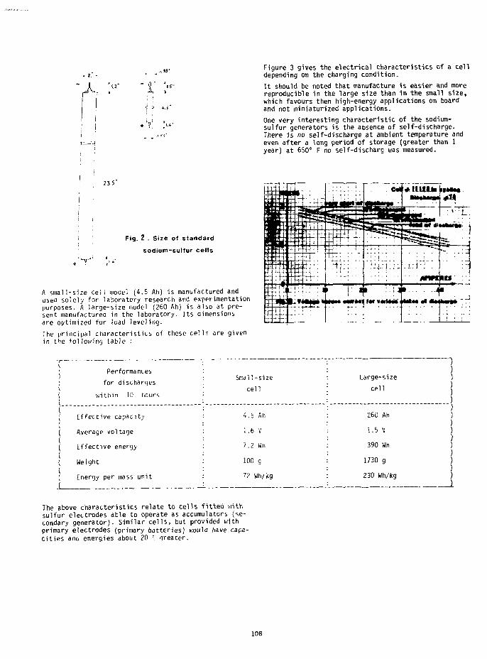
'(5-
t—-•-1
Figure 3 gives the electrical characteristics of a celldepending on the charging condition.It should be noted that manufacture is easier and morereproducible in the large size than in the small size,which favours then high-energy applications on boardand not miniaturized applications.
One very interesting characteristic of the sodium-sulfur generators is the absence of self-discharge.There is no self-discharge at ambient temperature andeven after a long period of storage (greater than 1year) at 650° F no self-discharg was measured.
235
Fig. 2 . Size of standard
sodium-sulfur cells
A small-size cell model (4.5 Ah) is manufactured andused solely for laboratory research and experimentationpurposes. A large-size model (260 Ah) is also at pre-sent manufactured in the laboratory. Its dimensionsare optimized for load leveling.
The principal characteristics of these cells are givenin the following table :
Performances
for discharges
within 10 hcurs
Small-size
cell
Large-sizeCPll
effective capacity
Average voltage
Effective energy
Weight
Energy per mass unit
4.5 Ah
1.6 V
7.2 Wh
100 g
72 Wh/kg
26C Ah
1.5 V
390 Wh
1730 g
230 Wh/kg
The above characteristics relate to cells fitted withsulfur electrodes able to operate as accumulators (se-condary generator). Similar cells, but provided withprimary electrodes (primary batteries) would have capa-cities ano energies about 20 " oreater.
108
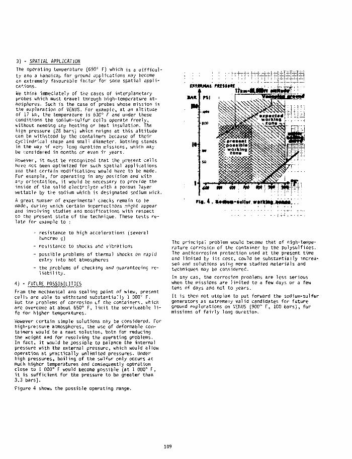
3) - SPATIAL APPLICATIONThe operating temperature (650° F) which is a difficul-ty ana a handicap for ground applications n;ay becomean extremely favourable factor for sotv.e spatial appli-cations.
We think immediately of the cases of interplanetaryprobes which must travel through high-temperature at-mospheres. Such is the case of probes whose mission isthe explaration of VENUS. For example, at an altitudeof 17 km, the temperature is 630° F and under theseconditions the sodium-sulfur cells operate freely,without needing any heating or heat insulation. Thehigh pressure (28 bars) which reigns at this altitudecan be withstood by the containers because of theircyclindrical shape and small diameter. Nothing standsin the way of very long duration missions, which maybe considered in months or even in years.
However, it must be recognized that the present cellshave not been optimized for such spatial applicationsand that certain modifications would have to be made.For example, for operating in any position and withany orientation, it would be necessary to provide theinside of the solid electrolyte with a porous layerwettable by the sodium which is designated sodium wick.
A great number of experimental checks remain to bemade, during which certain imperfections might appearand involving studies and modifications with respectto the present state of the technique. These tests re-late for example to :
- resistance to high accelerations (severalhundreo g)
- resistance to shocks and vibrations
- possible problems of thermal shocks on rapidentry into hot atmospheres
- the problems of checking and nuaranteeing re-liability.
4) - FUTURE POSSIBILITIES
From the mechanical and sealing point of wiew, presentcells are able to withstand substantially 1 000° F.But the problems of corrosion of the containers, whichare overcome at about 650° F, limit the serviceable li-fe for higher temperatures.
However certain simple solutions may be considered. Forhigh-pressure atmospheres, the use of deformable con-tainers would be a neat solution, both for reducingthe weight and for resolving the operating problems.In fact, it would be possible to balance the internalpressure with the external pressure, which would allowoperation at practically unlimited pressures. Underhigh pressures, boiling of the sulfur only occurs atmuch higher temperatures and consequently operationclose to 1 000" F would become possible (at 1 000° F,it is sufficient for the pressure to be greater than3.3 bars).
Figure 4 showb the possible operating range.
presentposalbtaworking, zon*
» m m w w *• w '
The principal problem would become that of high-tempe-rature corrosion of the container by the polysulfides.The anticorrosion protection used at the present timeand limited by its cost, could be substantially increa-sed and solutions using more studied materials andtechniques may be considered.
In any cas, the corrosion problems are less seriouswhen the missions are limited to a few days or a fewtens of days and not to years.
It is then not Utopian to put forward the sodium-sulfurgenerators as extremely valid candidates for futureground explorations on VENUS (900" F, 100 bars), formissions of fairly long duration.
109

wo
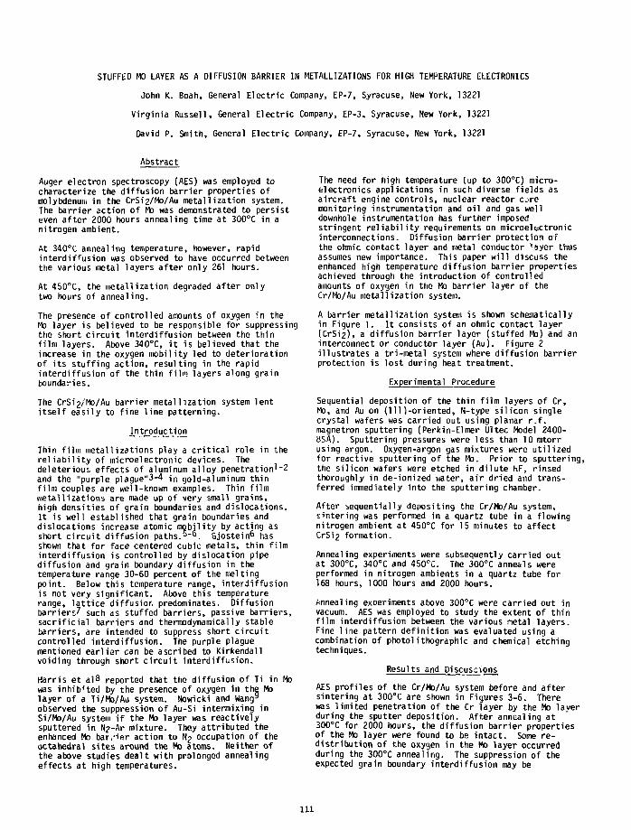
STUFFED MO LAYER AS A DIFFUSION BARRIER IN METALLIZATIONS FOR HIGH TEMPERATURE ELECTRONICS
John K. Boah, General Electric Company, EP-7, Syracuse, New York, 13221
Virginia Russell, General Electric Company, EP-3. Syracuse, New York, 13221
David P. Smith, General Electric Company, EP-7, Syracuse, New York, 13221
Abstract
Auger electron spectroscopy (AES) was employed tocharacterize the diffusion barrier properties ofmolybdenum in the CrSi'2/Mo/Au metallization system.The barrier action of Mo was demonstrated to persisteven after 2000 hours annealing time at 300°C in anitrogen ambient.
At 340°C annealing temperature, however, rapidinterdif fusion was observed to have occurred betweenthe various metal layers after only 261 hours.
At 450°C, the metall ization degraded after onlytwo hours of annealing.
The presence of controlled amounts of oxygen in theMo layer is believed to be responsible for suppressingthe short c i r cu i t interdif fusion between the thinf i lm layers. Above 340°C, i t is believed that theincrease in the oxygen mobility led to deteriorationof i t s stuff ing action, resulting in the rapidinterdif fusion of the thin f i lm layers along grainboundaries.
The CrSi2/'Mo/Au barrier metallization system lenti t se l f easily to fine l ine patterning.
Introduction
Thin f i lm metallizations play a c r i t i ca l role in ther e l i a b i l i t y of microelectronic devices. Thedeleterious effects of aluminum alloy penetration1-2and the "purple plague"3-4 j n gold-aluminum thinf i lm couples are well-known examples. Thin f i lmmetallizations are made up of very small grains,high densities of grain boundaries and dislocations.I t is well established that grain boundaries anddislocations increase atomic mobil ity by acting asshort c i r cu i t dif fusion paths.•>-<>. Gjostein^ hasshown that for face centered cubic metals, thin f i lminterdif fusion is controlled by dislocation pipediffusion and grain boundary diffusion in thetemperature range 30-60 percent of the meltingpoint. Below this temperature range, interdiffusionis not very signif icant. Above this temperaturerange, la t t i ce diffusion predominates. Diffusionbarriers? such as stuffed barriers, passive barriers,sacr i f ic ia l barriers and thermodynamically stablebarriers, are intended to suppress short c i rcu i tcontrolled interdi f fusion. The purple plaguementioned earl ier can be ascribed to Kirkendallvoiding through short c i r cu i t interdi f fusion.
Harris et al8 reported that the diffusion of Ti in Mowas inhibited by the presence of oxygen in the Molayer of a Ti/Mo/Au system. Nowicki and Wang9
observed the suppression of Au-Si intermixing inSi/Mo/Au system i f the Mo layer was reactivelysputtered in N?-Ar mixture. They attributed theenhanced Mo bar.-ier action to N2 occupation of theoctahedral sites around the Mo atoms. Neither ofthe above studies dealt with prolonged annealingeffects at high temperatures.
The need for high temperature (up to 300°C) micro-electronics applications in such diverse f ie lds asa i rcra f t engine controls, nuclear reactor cjremonitoring instrumentation and o i l and gas welldownhole instrumentation has further imposedstringent r e l i a b i l i t y requirements on microelectronicinterconnections. Diffusion barrier protection ofthe ohmic contact layer and metal conductor ^ y e r thusassumes new importance. This paper w i l l discuss theenhanced high temperature diffusion barrier propertiesachieved through the introduction of controlledamounts of oxygen in the Mo barrier layer of theCr/Mo/Au metallization system.
A barrier metallization system is shown schematicallyin Figure 1. I t consists of an ohmic contact layer(CrSi'2), a diffusion barrier layer (stuffed Mo) and aninterconnect or conductor layer (Au). Figure 2i l lustrates a tri-metal system where diffusion barrierprotection is lost during heat treatment.
Experimental Procedure
Sequential deposition of the thin f i lm layers of Cr,Mo, and Au on (111)-oriented, N-type si l icon singlecrystal wafers was carried out using planar r . f .magnetron sputtering (Perkin-Elmer Ultec Model 2400-8SA). Sputtering pressures were less than 10 mtorrusing argon. Oxygen-argon gas mixtures were ut i l izedfor reactive sputtering of the Mo. Prior to sputtering,the si l icon wafers were etched in d i lu te HF, rinsedthoroughly in de-ionized water, a i r dried and trans-ferred immediately into the sputtering chamber.
After sequentially depositing the Cr/Mo/Au system,sintering was performed in a quartz tube in a flowingnitrogen ambient at 450°C for 15 minutes to affectCrSi'2 formation.
Annealing experiments were subsequently carried outat 300°C, 340°C and 450°C. The 300°C anneals wereperformed in nitrogen ambients in a quartz tube for168 hours, 1000 hours and 2000 hours.
Annealing experiments above 300°C were carried out invacuum. AES was employed to study the extent of thinf i lm interdiffusion between the various metal layers.Fine l ine pattern def in i t ion was evaluated using acombination of photolithographic and chemical etchingtechniques.
Results and Discussions
AES profi les of the Cr/Mo/Au system before and aftersintering at 300°C are shown in Figures 3-6. Therewas limited penetration of the Cr layer by the Mo layerduring the sputter deposition. After annealing at300°C for 2000 hours, the diffusion barrier propertiesof the Mo layer were found to bs intact . Some re-distr ibut ion of the oxygen in the Ho layer occurredduring the 300°C annealing. The suppression of theexpected grain boundary interdiffusion may be
i l l
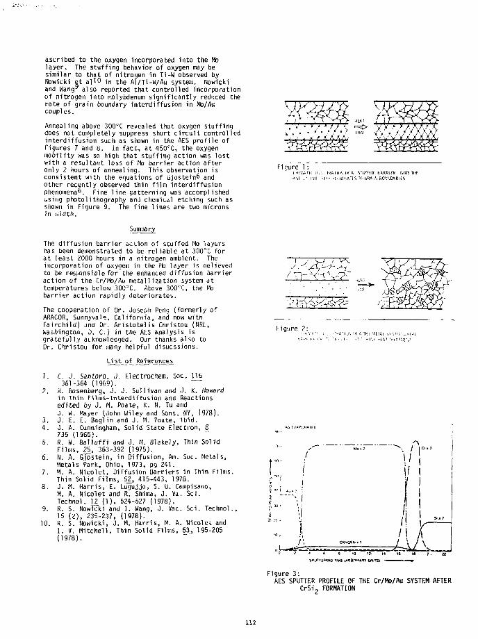
ascribed to the oxygen incorporated into the Molayer. The stuff ing behavior of oxygen may besimilar to that of nitrogen in Ti-W observed byNowicki et a l 1 0 in the Al/Ti-W/Au system. Nowickiand Wangy also reported that controlled incorporationof nitrogen into molybdenum signif icantly reduced therate of grain boundary interdiffusion in Mo/Aiicouples.
Annealing above 300°C revealed that oxygen stuffingdoes not completely suppress short c i r cu i t controlledinterdiffusion such as shown in the AES prof i le ofFigures 7 and 8. In fact , at 450°C, the oxygenmobil i ty was so high that stuff ing action was lostwith a resultant loss of Mo barrier action afteronly 2 hours of annealing. This observation isconsistent with the equations of GjosteinS andother recently observed thin f i lm interdiffusionphenomena . Fine l ine patterning was accomplishedusing photolithography and chemical etching such asshown in Figure 9. The fine lines are two micronsin width.
. . • • ' • " . ' ' ' TIME
y • f A A A A ,
Figure 1:( H C J A r i l I ' l l I R A N I ' . UFA STUFFED" BARRIER NOJE THE
• •••s[ . •> I'M '•• l u s i r t^iijATE S TO C.RA|\ BOUNDARIES
The diffusion barrier action of stuffed Mo layershas been demonstrated to be rel iable at 300°C forat least 2000 hours in a nitrogen ambient. Theincorporation of oxygen in the Mo layer is believedto be responsible for the enhanced diffusion barrieraction of the O/Mo/Au metallization system attemperatures below 300°C. Above 300°C, the Mobarrier action rapidly deteriorates.
The cooperation of Dr. Joseph Peng (formerly ofARACOR, Sunnyvale, California, and now withFairchild) and Dr. Ar is tote l is Christou (NRL,Washington, D. C.) in the AES analysis isgrateful ly acknowledged. Our thanks also toDr. Christou for many helpful disucssions.
List of References.
3.4.
10.
C. J. Santoro, J. Electrochem. Soc. 116361-364 (1969).
K. Rosenberg, j . J. Sullivan and J. K. Howard\n Thin Films-Interdiffusion and Reactionsedited by J. M. Poate, K. N. Tu andJ. W. Mayer (John Wiley and Sons, NY, 1978).J. E. E. Baglin and J. M. Poate, ib id .J. A. Cunningham, Solid State Electron, 8735 (1965).R. W. Ba l lu f f i and J. M. Blakely, Thin SolidFilms, 2b, 363-392 (1975).N. A. Gjostein, in Diffusion, Am. Soc. Metals,Metals Park, Ohio, 1973, pg 241.M. A. Hicolet, Diffusion Barriers in Thin Films,Thin Solid Films, 5£, 415-443, 1978.J. H. Harris, E. Lugujjo, S. U. Campisano,M. A. Nicolet and R. Shima, J. Va. Sci.Technol. 12 (1), 524-527 (1978).R. S. NowTcfki and I . Wang, J. Vac. Sci. Technol.,15 (2), 235-237, (1978).R. S. Nowicki, J. M. Harris, M. A. Nicolet andI . V. Mitchel l , Thin Solid Films, 53, 195-205(1978).
Figure 2:I . . • - . - . • | ) - . '..) A I K i \ U ! A [ b v S T - V . • . ' • ( - •
SPUTTERIMG 1IME (ARBlTRARV UNITS)
Figure 3:AES SPUTTER PROFILE OF THE Cr/Mo/Au SYSTEM AFTER
CrSi2 FORMATION
112
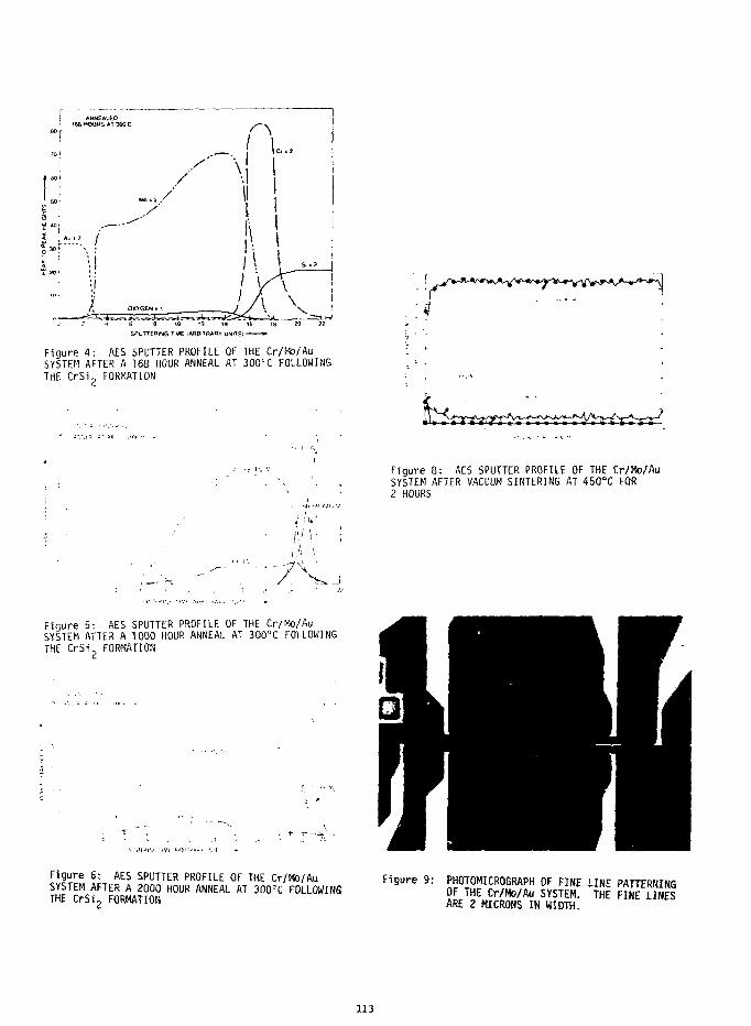
SPUTTERING TIME IAR0ITRARY UNITS] -
Figure 4: AES SPUTTER PROFILE OF THE Cr/Mo/AuSYSTEM AFTER A 168 HOUR ANNEAL AT 300cC FOLLOWINGTHE CrSi2 FORMATION
Figure 8: AES SPUTTER PROFILE OF THE Cr/Mo/AuSYSTEM AFTER VACUUM SINTERING AT 450°C FOR2 HOURS
Figure 5: AES SPUTTER PROFILE OF THE Cr/Mo/AuSYSTEM AFTER A 1000 HOUR ANNEAL AT 300°C FOLLOWINGTHE CrSi FORfiATION
Figure 6: AES SPUTTER PROFILE OF THE Cr/Mo/AuSYSTEM AFTER A 2000 HOUR ANNEAL AT 300CC FOLLOWINGTHE CrSi2 FORMATION
Figure 9: PHOTOMICROGRAPH OF FINE LINE PATTERNINGOF THE Cr/Mo/Au SYSTEM. THE FINE LINESARE 2 MICRONS IN WIDTH.
113
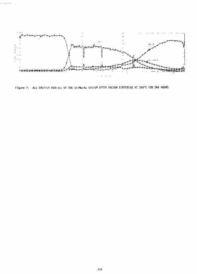
F i g u r e 7 : AES SPUTTER PROFILE OF THE Cr/Mo/Au SYSTEM AFTER VACUUM SINTERING AT 34O°C FOR 264 HOURS
114
REFRACTORY GLASS AND GLASS CERAMIC TUBE SEALS
Clifford P. Ballard and Donn L. StewartSandia National Laboratories
Albuquerque, New Mexico 87185
Complex vacuum cube envelopes are required tohouse and support integrated thermionic circuits (ITC)during long-term operation at elevated temperatures.Li-O-ZnO-SiO glass ceramic and CaO-A^O- glass seals
were investigated because they are refractory,moldable, have relatively high thermal expansioncoefficients and bond directly to a variety of metals.
Materials and techniques were developed tofabricate the silicate glass ceramic (o5OO°C = 10 Qm;Tg = 450°C) into a toroidal tube design containing64 Pt/Rh feedthroughs. Subassemblics were exposedto 600°C for periods in excess of 140 hours with nodeterioration of vacuum seal integrity. However,lithium ion conductivity reduced lead-to -]eadresistance below 1 megohm at 350°C, yielding adevice unacceptable for ITC applications.
yThe calcium aluminate glass (p5uO C = 10 Qm;
Tg = 900°C) contains no alkali but is more difficultto fabricate into complex shapes. Special transfermolding techniques were developed using pre-enameledmetal piece parts. These subassemblies were vacuumtight, had a lead-to-lead resistance of 20 megohmsat 600°C and are believed acceptable for ITCapplicat ions.
115
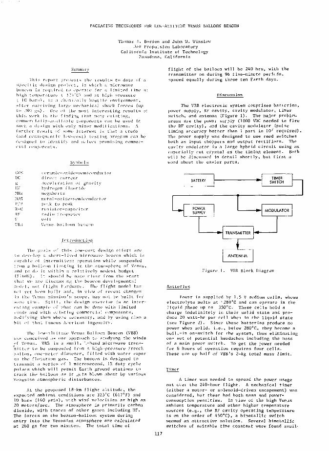
PACKAGING TECHNIQUES FOR LOW-ALTITUDE VENUS BALLOON BEACON
Thomas .1. Borden and John \J. WinslowJet Propulsion Laboratory
California Institute of TechnologyPasadena, California
Summary
Thi s report present s the u'.sults to da te of a
spec i * ic des ign pro jre t, in wh i ch a microwave
beacon is requ i red tu operate for a 1imi ted t ime at
h i gh temperature ( '3 J V C ) and ;IL h igh pressure
{ I 0 bars) , i n a jheiiiica I 1 y host i le envi ronment,
a t £.e r surv i v ing large- f.iorh.tn ic.i ] shock fore ex (up
tti ._'8O gs) . One oi" the most interesting results of
this work is the f ind ing that many existing,
commerc ia 1 I y-avii i 1 able cumponen ts ran be used in
such a design with only minor modifications. A
i ur ther res.i ] L of some interest is tha t a crude
(and conseqnen t1y lew-cost) testing program can be
des i gned to id en t i I > and se I ec t promi s ing commer-
c ia1 component s.
flight of the balloon will be 240 hrs, with the
transmitter on during 96 five-minrte perieds,
spaced equally during those ten F^rth days.
Discussion
The VBB electronic system comprises batteries,
power supply, RF cavity, cavity modulator, timer
switch, and antenna (Figure 1). The major problem
areas are the power surply (1000 VDC needed to fire
the RF cavity), and the cavity modulator (pulse
timing accuracy better than I part in lO'' required).
The power supply was designed to use reed switches
both as input choppers and output rectifiers. The
cavity modulator is a large hybrid circuit using an
especially cut crystal as the timing element. Both
will be d iscussed in detai1 short 1y, but first a
word about the easier parts.
COSDCgIII"
MHzMO.S171 1
R-I:RI-"
V
VBii
ccrnm ic-cx idv-st'iu ici-'iuhictdi rec t current.lcce 1 era I ion ol" gravitvhvdroj;en 1 luoride
megahertzmetn 1 -o>: ide-sem L-onduc torpe.-.k tu peakres i stor-capnr i torradio f requency
V I . I L
Venus balloon be.-icnn
In t ruduction
The goa 1 s of th is 1ow-cost des ign effort are
to develop a short-1ived microwave beacon which is
capab1e oi i nterm i t ten t operat ion while suspended
1 rom a ha 1 1 oon f 1 oat i ng in the atirmsphere of Venus,
ami to do it within a relatively modest budget
($lf>OK). It should bt- made clear from the start
t h;> t we ari1 d iscuss . ng the beacon developmental
model, not flight ijrdware. The flight model has
not yet been built and, in view of recent changes
in the Vt mis missi on's scope, may not be bullt for
some time. Still, the design exere i se is an inter-
est ing ex.imp 1 <_• tif ".-'ha t can bv done wi th 1 iroi ted
iimds and with existing commercial components,
modifying them where necessary, and by using also a
bit of that famous A.*ic?r ican ingenu i ty.
The low-altitude Venus Balloon Beacon (VBB)
ua.s conee i ved as one approach to study ing the xcinds
of Venus. VBB is a sma 11, '.-band mi crowave trans-
"mitter to be suspended f rom a h igh-pressure French
ballon, one-meter diameter, filled with water vapor
as the f i o'.at ion gas. The beacon is designed to
t ransm it a series of 1 microsecond, 1% duty eye] e
pulses which will permit Earth ground stations to
t truck the bal loon .i.s it gets blown about by various
Venus ian atmospher ic disturbances.
At the proposed 18-km flight altitude, the
expec ted ambient condit ions are 325°C (617°F) and
10 bars (160 psia), with wind velocities as high as
20 meters/sec. The atmosphere is primarily carbon
dioxide, with traces of other gases including HF.
The forces on the beacon-balloon system during
entry into the Venusian atmosphere are calculated
at 280 gs for two minutes. The total time of
BATTERY
POWERSUPPLY
M1TTER
TIMERSWITCH
MODULATOR
ANTENNA
Figure 1. VBB Block Diagram
Ba t t e r i e s
Power is supplied by 1.5 V sodium cells, whose
electrolyte melts at •280°C and can operate in the
liquid phase up to 35OCC. These cells hold a
charge indefinitely in their solid staLe and pro-
duce 20 watt-hr per cell when in the liquid state
(see Figure I). Since these batteries produce no
power when solid, i.e., below 280°C, they become a
buiK-in on-switch for rhe system, thus eliminating
on" set of potential headaches including the mass
of a main power switch. To get the power needed
for 8 hours of operation requires four cells.
These use up half of VBB's 2-kg total mass limit.
Timer
A timer was needed to spread the power usage
out ovei the 240-hour flight. A mechanical rimer
(either a motor- or solenoid-driven escapement) was
considered, but these had both mass and power-
consumption penalties. In view of the high Venas
ambient temperature and other higher temperature
sources (e.g., the RF cavity operating temperature
is on the order of 45O°C), a bimetallic switch
seemed an attractive solution. Several bimetallic
switches of suitable time constant were found avail-
117
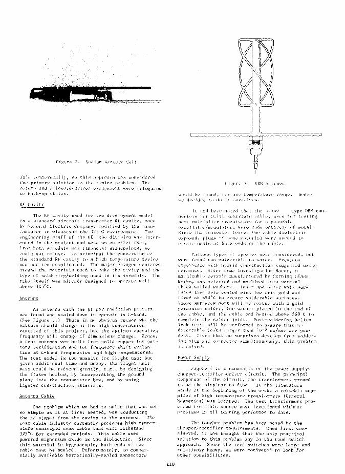
Figure 2. Sodium Batt.ery Ce!I
.ibl e I'oniniLTc in 1 iy, HO thin approach v.'fs eons ide we!
the pr i mary so 1 ution to the t imini: prob I em. The
motor- and so}om>id-dr iven escapement wore relegated
to bark-up stntus.
RK Cavity
elopment moRF cavity,t*U by the .ni ronmtni:.vision wasoffer that.
andpo int.s1.conve rs i on
mperature dchanges ce
delmadeanaTheint
We
ev inte
ho civ i ty andts asseinblyupera te we I I
-
er-
redtheThe
The RF cavi ty used for the dev
i s a s Land a rd a i re ra t" L t ransponde r
by Uener.iJ HI eetr ic Company * modi f i
rncturpr to withstand thy "i?5 "C i'Viv
engineering staff of the r.E t'lhe di
ested in the project and made us an
f rora both schedul e and t inane In I sL
;'nu Id not. re fust1. In pr inc *pai the
the standard RF rav icy tt> ;i hi #h te
u-tiH nut too cornel icntod. The ma jor
around the m;itcr ials used to make 'J
type oi sol dor i rg/veld ing used in i
tube, itrie I f was al renOy designed to
above 325""C.
Antenna
An antenna with the pi. per radiation pattern
was found and scaled down to operale in L-band.
(See Figure 3.) There is no obvious reason why the
pa t tern shouJ d change a t the h igli tempt? ra Lures
expected uf this project, but the optimum operating
frequency will change if dimensions change. Hence,
a test antenna was built from solid copper for pat-
tern verification and Fav frequency-shiCt evalua-
tion at L-band frequencies and high temperatures.
The tost model is too passive for flight use; but
given additional time and money, the flight unit
mass could be reduced greatly, e.g., by designing
the ftnkes hollow, by incorpurating the ground
piane into the transmitter box, and by usinft
lighter construction materLals.
Antenna Cable
One problem which we had to solve that was not
so simple as it at first seemed, vas conducting
the RF signal from the cavity to the antenna. The
coax cable industry currently produces high temper-
ature semirigid coax cable that will withstand
325°C for extended periods. This cable uses
powered magnesium oxxde as the dielectric. Since
this material is hygroscopic, both ends of the
cable must be sealed. Unfortunately, no commer-
cially available hermetically-sealed connectors
rigure i. VBB Anu-nm.
c; «u 1 ci bt> t'niind , tor .inv t einpc r,j tut"*.' range. iiiMiee
we tk'i- id i'd 1" do it. .nir^e 1 vi-s .
I t had been n*>U'd (.hat the -u and type OSM con-nee tors for 0. I A 1 semi r Lj;id cable, usen fur test inv;some ntil t fplier transistors S'or a possibleuse i J ]/jtnr/mi*dulatur, were made uiHirely oi mt'ini .S inee Lhe eon nee tor t i_-aves ' lie cab 1 e d ie Ler t r ieexposed % p lue,s -i ;-.U«K* irati*; i i\ 1 were needed Locreate seals at. boCi\ vnvlti of the c;ible.
Var Lous types <••!" cpoy. ivs were n m s idered, butwere found Loo vulnvrnble Io water. Prev iousex per i ence w I Lli liybr i d cons t rue t ion .surges t ed us i Uf,eeramLcs. After some i nvest i gat ion Macor, amac hi nab le cerami r n};nt»l\-u:tu red by Corn ing f, LassWorks, was so I ecteii and machined in to severalthiek-walled washers. Inner and outer wn11 sur-faces then were coa tec! with I ow frit jiol d andf irt'd at 850°C tn create sfilderab] e surfaces.'I'liese surt aces next will he coated wi tli a gol dgermanium solder, the washer piaced in the end ofi.he cnbi e, and the cable end heated above 360 C toeompl ete the so] der join t . Post-scildering heliura1eak tests will be performed to assure that nntie tec tab 11* 1 e;:ks i arger than I 0~9 Cc/see are pre-sent . Given that no surprises develop from solder-ing plug and connector simultaneous!y» this problemj s solved.
Power Supj: iy
Figure 4 is a schema Lie oC the power supply-cliopper-i ect j fi^-r-driver c i rcui t. The pvinei palcomponent of the c i rcui t the transformer, provedL O be the i: imp test to find. In the literaturestudy at the beginning of the v>rk» n reliat?] i sup-plier of high temperature transformer? (GeneralMagnetics) was located. The test transformers pro-cured from this source have functioned withcutproblems in all testing pen'ormed to date.
The tougher problem has been posed by thechopper/rectitier requirements. When first con-sidered, it was thought that the only practicalsolution to this problem lay io the reed switchapproach. Since the reed switches were large andrelatively heavy, we were motivated to look forother possihilities.
118
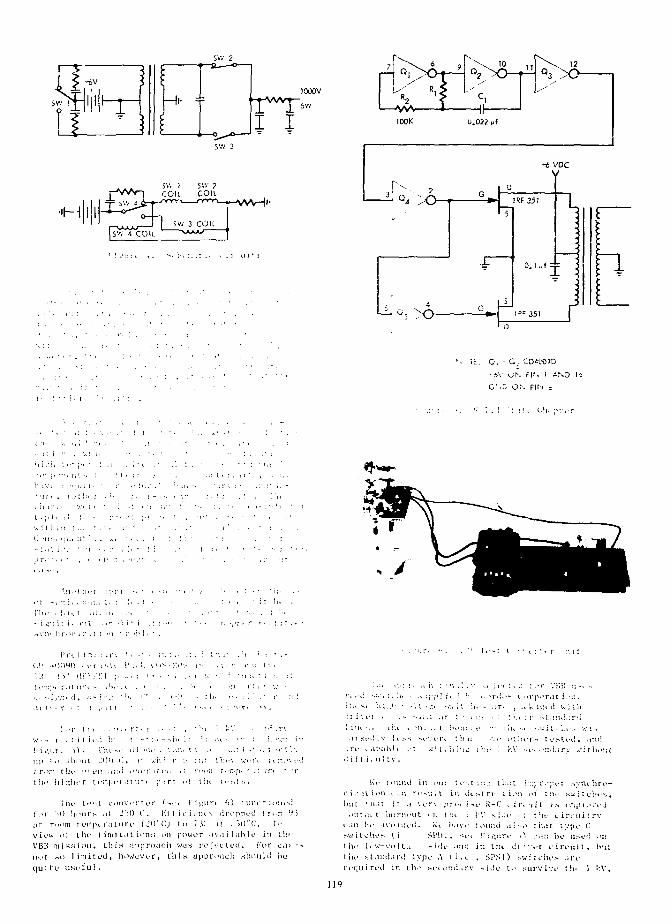
> --6V
T
SW 2
~t—a—o
FT
. " 1. O, - G - CD^00?D
*6V ON r IN I AND 16
O'-C/ ON FIN fc
' i i : ! i * i " ' 1 ;•> i :'. , i < . . :
• ' j r < , i . i t i n : : '•< -, ;••
u i t h i n [ i n t ;• . : • : '
. • n « ' i i n - r ! p r - r : • t . - - ;
\ i . S • '-' O s i • • • . ;
. ! - - i , ; n . ( J , u - i f . - :
• ' • - i : t ' r i - i *
i ;• . . - - r ^ : . ^ t o r p o r . u i .>:•! .
i i : i . - . i r . ; • ... k . i >; * t i u i i i i
! . T '. " n t i > ' v . i r ; • ; . - • ; . " - - t •. ,- . • . : : • , r \
w . i s I , - . ! i l i c . i ! r , ' " - * ! • • - - . t i t i : : : • : < -. ' •• ; ;: ".-;:: i n
!• i / , u u ) ) . r h e - t L i i ' . . : ,• . : u ' . i . u .* - s * i - " - . t > ! • [ ' . - .
u p i n . i t i o u t _ : O I ] C, i t A I I i i 1 ;•• i v , ' l v . < - \ • « • < • : * < n , : - . , i l . f < l
; n>. - t h e I ' I V I I . uu l O I X T J U - U H r-•>':? r ,-;;-p, r .: tir« ' Tt h e i i i : ' I H T u - v i p i - r . i i n r ( p . i r t o t t iu t r s i s .
1'lie t e s t e o t i v e l ' L e r ( s e e I" i £ u r i ft) * u n c t i o n e df o r "iO h o u r s <U J 3 0 (". Kl t i r i i ' iu > d r o p p e d ! n.ir. l.Ma t r o o m t einju r n t u r e ( J O ' C) t o 7 3 ; it _ j | ) " f : , 1 ;•v i c w o f t l ie i im i t . ) t i o n s o n p o w e r ,-iv.i i l . i h I e i:i t h eI'BB m i s . s i t u i , t h i s ; i p p r o a c h w a s r e j e c t e d . T o r c . u •-.n o t s o 1 i m i t e d , h o w e v e r , t h i H a p D i ' o p . c h s l i o u l d he1
q u i . ti> u s u l u l .
•" ; I t - ••- ^ ' .v i l . '..,.•
r i , - .u i o n *...;•. i v . - \ : l t i n t i i - s t n - L i ,>n of : : H s v i ; u l u - s ,imL * li . it i : .i V I T \ p n - t i s e K - C t i r < ' r i t i ^ i - . - n o v e JM t i t i N t i)i:t"!i<Hit ' r. i \;v \ !'V s i J i ' . •: : h f ». i r c u i i r v
c.ii7 b f . I V I M :U'Li. rt\ fi.svo i o u i u i . i : •..' t i i . i t . L v p o Csv; itv;l\v*s t, i SIMl. , •;.•! i ' i r . u r t - ^. / . i : : b e us i - i i ^ nL'ne l . w - v n l t . i - i d e . I : U : i r . t t u - d i : " t * r c i r c u i t , h u ttiu> . s t . a iHl . in i t y p e A ( i . e , S P S I ) s w r i f J u ' s . j n -r e q u i r e d i n Ow s n u m l . t r y * - i J c t o s u r v i v e ; h f « >'A".
119
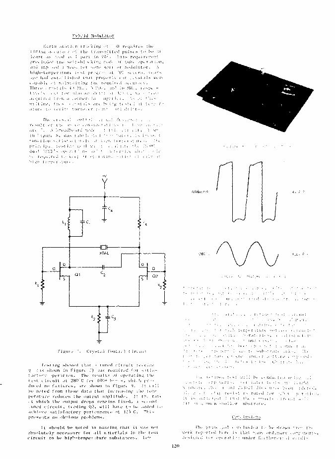
?~yfu id Modulator
fc.irt !i > i , i t i o n i r - n k i n j ; . i t " i B r v t j i i ' r i > ; h e
i o a s t . , * . - . s u J *-> i ; M r t i n i O 7 - l ' l i i s r r < j ; i i r . - : : : , - : U
. ) : H } j u . p .~.,_-d .1 : u - e . . ' . o r v « B i t - s o r t n f ; : , .w i i i I a t o r . A
. 1 ^ 0 h . u i c . s t * > " ' l i s l u ' i i t h a t p r o j d - r h n i l . . \ s i . i l * u v n
<. . t p . i h 11- . ' 1 r . . j i m .i i n i n * : 1 J u - r e q u i r v . i . H . U I . H V .
T h r e e , r v . - s t a l * - ( i Mi : . . , "i ' . ' ; ) . • , 1:1.1 : u N h V , u ' S ' . . -
t i \ \ ' ! \ 1 i ; 1 I i T "•: i n t . . . u : " i i v '. ' \ • . ' . " . . ' ' • \ , ? i ( • ' < < • : •
. i t t ; u i i " t t £ ; i " ' T , ; . ( . n : r : c r i i . i L i p ; 1 1 1 1 1 . ' o - o : f ' i . *-
r i \ * . ( - . ^ . . l i . o n : r - i . 1 1. i '- <.\K - ; :-\. •- .
r*. -~u) l . ' [ t h e 0 \ •• v o n - :.u r : ' : - : , - 1 •• i . •,-::• i i . • , . -
: v i : u - 1 i . M I i . . : i ^ : . n I •••' ' ] •• . ; t , t / * . v . - • , • . « 1 r. , i v , - . ; >.<•
l i v i . . i K - ' ) ! ' ! * - - . ' p i r . [ . si?- i n '. : ! . i - r " - ? , > : , ! : : : . " ! . :
i n - r c ' . , i ! i | - i \ ! I ' - f . f [ ' t o ; • t : 1 ; : ; , - . ; j o . t ; : '. v : r
h : i i h t r : " p i - r - t m . .
v
t, > =FC
HDI-XTAL
Ql C,Q 2
r* c
PL-SI i n g showt-d i: h . i t ! t i n i f d r i r n i i t ; t i i ; i::.:'J (-i.-: sr-.m-Ti i n !•" I j ; u r f 7) .'.KS rc-m: t r o d r ^ r > i i : ; • -5 -li." t t f v ' p t T . j i i o n . The r c s i i \ i s of opt-r.f t i nii t in.'tL'Kt L i r a i i l -u 2 8 0 C N-r 100+ b>--*, whi.-li p r . -<liu L-tl -no f a i l u r e s , i r i - ^hnwn in F i g u r e l). ll > i - :ht- n o t e d f rotn t l i e s f d;it>J t h.ii i m r i - . i s i n r i iic t r:";-p t ' r a t '.ji"L- r t ' d u c t ' s Chi* i ^u tpu t amp] i tud*-. I : t *v r . i i .. t w h i c h tin* o u l p u t d r o p s rc:nn i n s f iy.i 'tl, ,i M t .-nd. u n e d c i r c u i t , f * od i n g Q 2 , u'i 11 h. ive t " (u- ,Kid*Hl i .. i vh i ' - v i - s*it ia(.ictnry p » r f o r n ; i n n - -u U i ( ' . Ti: i •-p r ^ s v i t s no o b v i o u s p r o h ! e m s .
I t s h o u U i b e n o t e d in p a s s i n ii t h a t i t v;.\^ n o tA b s o l u t e l y n e o ^ r i s - i n / f o r a l l R. i t e i* i , j ) S in r'fu- c t*stt" i r c u i t t o b e h i p ^ ~ t e m p e r i t u r e sub . -ua I C ^ ' S . J-c1-.'
t t i' i r
-1 ; ' . . . . \: • i ::• • r . -; . . :-. m :
" - o > ;v . • a n . : < •; •- . ; • . • } . . -
i - v - i - : : • - r . i l t - i i : . * r ••."> ( p r » : i -
rk rep T ; i ! i v o r t ! . : i , i t v r ^ r - . p . ' - ^ n 1
120

Cion.s, nay be us , <i in . :-:t rt-i:u. t
e l thiT ".is i - , *' or vi t h - . i •! • •
i n t h i * i r . - . - n - . : r <i< I i ; : . \ < r
. l h i 1 i [ U ^ - * . i - - 1 . ; : 1 > i i n •. ; . : > . i
h a s h t v i i . i n , : - , - " . : , A '-•; l \ u : i , , r < - ' - . ; r i • : • - ; i
1 • - - : , r • >; r<
: r * : . r v M i r « h p i - : : : • r r . v i i . . t
121
HIGH m n u n u nsnunca tm mart mien oamcms
by
Henry Walker, Director of Re«earch, Penuluster, Inc., Burbank, California
SMUEI
The search by the electronic industry for componentsthat are light weight, more compact, are capable of operat-ing in very high, temperature and all environmental condi-tions is now proving rewarding.
The properties of such a flexible, transparent, thinfilm of aluminum oxide insulated wire or s t r ip (with aaelting point of 2050°C.) is unique for applications in theelectronic, missile, atomic reactor, aerospace, and aircraftindustries. The oxiae filn is highly flexible, suitable fora l l windings of any size and shape of coil (magnetic).Briefly touched upon are the ultraviolet, proton gamma ra-diatiou uses, as wel1 as high vacuum and cryogenic applica-tions.
Since the filtn is inorganic and chemically inert, itdoes not age or deter iora te in storage and has gooddie lec t r i c propert ies (1000 vol ts per n i l ) . In brief,components designed around this unique material will keepabreast of present day and future tect. x)logy.
Designers of e iectro-oagnetIC conponents can nowachieve higher ratings per unit of weight and 3 reduction insi~e. With proper design, less insulation v i l l be requiredand the dielectric losses art reduced.
The use of an aluminum conductor (round or rectangularwire or strips) will save bOX in weight, which is a distincticiprovetoenl 11. commercial applications such as linearmotors, Cic-dical instruments, etc., where lower mass willresult in lover inertia. Rotary equipment with low masssimplifies dynamic balancing. As vibration from dynamicimbalance is reduced, greater sensitivity and improved highfrequency response in moving coil applications results fromthis lower aass. In a l l , it is a dream cone true for mostengineers.
Compared to copper, aluminum with AljO-j insulationoperates cooler and will not oxidi'e. When operating temp-eratures of above 100° C, copper will form an invisiblefilm of cuprous oxide; above 200° C. cuprous and cupricoxide are formed readily on the surface, thus reducing theconductance as ultimately severe corrosion occurs and even-tual ly the conductor i s rendered useless. Even nickelcoated copper is subject to a galvanic action of the twometals. In a high temperature operation, migration of atomsis created.
Performance of electrical components in high tempera-ture is seriously handicapped due to the lack of suitableinsulat ing materials as the components are subjected tosevere physical stresses in environmental conditions. Whenfailure occurs in organic insulation, the failure remainspermanent owing to the electrically conductive carbon paths
that are formed throughout the insulation as well as otherendangering problems, such as lack of adhesion, oxidation,evaporation, :*nd aging.
Aging is accompanied by weight loss in organic naterialwhere shrinkage result* in the resin portion causing it tolose i t s bond in the slot c e l l s , thus creating fai lure-Variation of temperature or rotating speed causes mechanicalabuses of the insulation. Thermal degeneration is fasterclose to the current-carrying conductors where the tempera-ture is at a maximum; Therefore, the failure is induced atthe hottest spot of the winding.
Aluciinuci conductor and Al>jG-i insulation, which is cer-amic in nature, is free of galvanic action or oxidation. Incase of a breakdown, the insulation does not create trackingof a permanent conductive path throughout the insulation.In fact, oxide from the air creates a new insulated oxideand could repair itself. Therefore, it is a good reason toconsider the re la t ion between operating temperature andinsulation l i fe . A component aade with high tenpertureinsulated material will be more reliable and will protectitsell and its payload from instant heat and pressure.
camerasFor several decades aluminum has been successfully em-
ployed in the electrical engineering field and in variousother applications such as in transformers, generators,etc., using bulky interleaving materials such as paper,plastics, or laquer as insulation—far from satisfactory.
TABLE I—Thermal and electrical conductiv.tics olaluminum and copper.
Aluminum for electric conductors has a resistance of
about 34.5 ohms/mm , which is equal to approximately 62% of
the conductivity of electrolytic copper. The specific
weight is 2.7 gm/cm , or about 30% of that of copper. This
means that an aluminum conductor of equal conductivity
weighs only 501 of tnat of a comparable copper conductor.
In many cases, depending upon design, the conductive weight
can be further reduced depending on the dielectric loss, as
aluminum operates cooler, and dissipates heat more rapidly.
Copper clad aluminum wire is re-inforced with EC grade
aluminum conductor of an improved design developed to give
electric power new versatility in construction. In addition
to the contribution of its high strength to the conductor,
it adds to the total conductivity of the conductor, so that
it performs a dual function of strength and conductance. Of
123
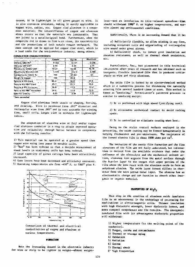
course, it is lightweight in all given gauges of wire. Itis also corrosion resistant, making it easily applicable tomagnet wire, cables, etc. Copper clad aluminum is a compo-site material; The interdiffusion of copper and aluminumatoms occurs so that the materials are inseparable. Theyare joined in a metallurgical bond. Furthermore, when thecomposite rod is drawn to fine wire sizes, its concentricityand the proportions of both metals remain unchanged. Thesame concept can be applied for copper clad steel, which isa lead cable for the semiconductor industry, among others.
CONDUCTOR CHARACTERISTICS
Densily tBS/IN3
Density GM/CM3
Besist.Kity OHMS/CMFResistivity Microhm-CMConductivity MACS %)Weight % CoppeiTensile KPSIHardTensile KG/MM2 HardTensile K PSI-AniiediedTensile KG/MM2-AnnealedSpecific Gravity
Capper0.3238 91
10.371.724100
100
65 046.735.024 68.91
Cu/AI0.1213.34
16.082.W3
61-6326.830.021.117.012.03.34
Aluminum
0 0932.71
16.782.790Gl
27.019.017.0'12.02.71
'Semi annealed
Copper clad aluminum lends itself tc shaping, forming,and drawing. Wire is produced from .003" diameter andrectangular wire from .001" and is very suitable for windingfine, small coils. Larger wire is suitable for lightweightcables.
The adaptation of aluminum wire or foil and/or copperclad aluminum conductor is a step to attain improved opera-tion and reliability through better balance in componentswith the following results:
1) This material can be operated at a greater speed thancopper wire using less power in movable coils.
2) 'Mum" has been reduced so that a decible measurement ofsound levels in stationary coils has been reduced.
3) Load capacity of given ratings have been effectivelyincreased.
4) Core losses have been decreased and efficiency increased.5) Operating temperatures are from -450° F. to 1000° plus F.
\
• ! •
:
h\j-——^-^—*~
11
!
IP ' J
^ J
TEMPERATURE. °C
Comparison of thermal and electricalconductivities of copper and aluminum atvarious temperatures.
FORMATION
Note the increasing demand in the electronic industryfor wire or strip to be lighter in weight—almost weight-
less—and an insulation so thin—almost spaceless—thatshould withstand 1000° F. or higher temperatures, and sur-vive almost any environmental conditions.
Additionally, there is an increasing demand that it be:
a) Sufficiently flexible, to allow winding in any form,including miniature coils and edgewinding of rectangularwire wound under great stress.
b) Sufficiently thick, to insure good insulation andabrasion resistance, as well as thermal shock resistance,etc.
Permaluster, Inc., has pioneered in this technicaladvancement after years of research and has obtained such aninorganic, flexible insulated film that is produced contin-uously on wire and strip aluminum.
The oxide film is formed by an electo-chemical methodwhich is a conversion process for thickening the naturallyoccur ing film several hundred times or more. This method isknown as "anodizing." Perinaluster's patented process issimilar to anodizing except:
1) It is performed with high speed (justifying cost).
2) It eliminates mechanical contact to avoid rackingspots.
3) It is controlled to eliminate crazing when bent.
Owing to the strict control methods employed in theprocessing, the oxide coating may be formed homogeneously invarying thicknesses and pre-structures. The resistance ofthe formed alumina film is about 1800 ohms per cm .
The mechanism of the anodic film formation and the finestructure of the film are not fully understood, but informa-tion is derived from the available evidence that under theinfluence of the elctrolyte and the mechanical solvent ac-tion, aluminum ions migrate from the metal surface throughthe barrier layer to the oxygen rich upper portion of thefilm where the ions react with the aluminum oxide to form ananhydrous alumina. The oxide layer formed differs in char-acter from the more porous outer layer. The alumina has anelectrostatic charge and can function to absorb other inor-ganic or organic material.
FKWDTIZS OF
This step in the creation of aluminum oxide insulatedfilm is an advancement in the technology of processing forapplications in electo-magnetic coils. Thinner insulationwith high dielectric strength, lower dielectric loases, andmore compact components are the results. The inorganicinsulated film with its advantageous dielectric propertieswill withstand:
1) Higher temperature (to the melting point of theconductor).2) Fungus, corona and contaminants3) Thermal or storage aging4) Oxidation5) Radiation6) Corona
7) Thermal shock8~* High frequencies
124
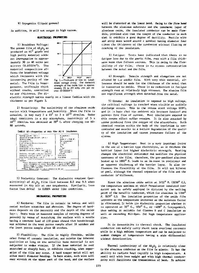
y
/
/
9) Cryogenics (liquid gasses)
In addition, it will not outgas in high vacuum.
ELECTRICAL PROPERTIES
1) Breakdown Voltage:The porous film of AI2O3 asproduced on EC2 grade andhigh purity material with-out impregnation is approx-imately 30 to 40 volts permicron (0.00004"), Thematerial composition af-fects the breakdown voltagewhich increases with theincreasing purity of themetal. The film is homo-geneous, uniformly thickwithout cracks, controlledto any thickness. The d i -electric strength varies nearly in a linear fashion with thethickness as per Figure 3.
2) Resistivity: The resistivity of the aluminum oxidevaries with temperature and humidity. When the film is
7 17unsealed, i t may vary 7 x 10 to 3 x 10 ohiis/cm. Underideal conditions in a dry atmosphere, resistivity of 5 x10¹⁵ ohms/cm, was obtained at 20° C. after charging tor 60-80 seconds.
TABLE IV—Properties of thin dim Al 0 Insulation.
0 axay rouvr w»:5-Fig. 1—Thickness of film vs. break-down voltage (rms). The dielectricstrength of the oxide film is approx-imately 35 to 40 volts rms per mi-cron (0 00004")
3) Dielectric Constant: The dielectric constant (per-mittivity) of AljOj film lies between 8.5 and 9.5 whenmeasured in dry air at one megahertz. Similarly, lossfactor (tan delta) is 0.0004 under like conditions.
tBCBAHICAL PROPERTIES
1) Hardness: The film is ceramic in nature and willresist surface scratches and abrasion. The degree of hard-ness depends on the porosity and the depth of the oxidelaypr. Tests made on numerous samples of varying degrees ofporosity by means of scratching the surface with a needlehaving a constant load of 130 grams showed that breakthroughwas achieved in the most porous sample after 16 strokes andthe least porous sample after 48 strokes.
2) Flexibility: The film is highly flexible, unlikeother forms of ceramic insulation, and retains the inherentqualities as long as the metallic base material is notsubjected to undue strains. If the base material is overstretched or sharply bent, it exhibits cracking, when separ-ation of the film may occur. A hard temper metal will notallow small diameter bending. In bare state, such wire willover stretch on the upper part of the bend, and the surface
will be distorted at the lover bend. Owing to the firs bondbetween the aluminum substrate and the innermost layer ofaluminum oxide, the insulated conductor can be made flex-ible, provided also that the temper of the conductor is suchthat it exhibits a good degree of ductility. Ductile wireand strip were wound around a mandrel having diameter fourtimes the thickness of the conductor without flaking orcracking of the insulation.
3) Fatigue: Tests have indicated that there is nofatigue loss due to the anoHic film, even with a film thick-ness more than fifteen microns. This is owing to the flex-ibility of the film; there is nj stress concentrationbetween the metal and the film.
4) Strength: Tensile strength and elongation are notaltered by tiie anodic film. With very thin material, al-lowance should be made for the thickness of the metal thatis converted to oxide. There is no reduction in fatiguestrength even at relatively high stresses. The alumina filmhas significant strength when detached.from the metal.
5) Corona: As insulation is exposed to high voltage,the critical voltage is reached when visible or audibledischarge occurs. This is the corona start voltage (CSV),and it is here that the ambient air becomes ionized andpermits free flow of current. Most insulations exposed tothis corona effect suffer erosion. It is also attacked byozone produced from the oxygen of the atmosphere. Suchchemical erosion within the body of the insulation is con-centrated and results in a serious degradation of the quali-ty of the insulation and causes premature failure of thesystem.
6) High Temperature: Heat is a very important factorin the use of a barrier type electrolyte, as it thickens thebarrier layer for higher dielectric strength. Heatingchanges the electrical resistance and modifies the physicalConstance of the film; therefore, the pre-anodized alutaimcnheated up to 1000° F. leads to an increase in resistance andan apparent thickening of the barrier layer. It also in-fluences the flexibility of the film. It will not blisteror peel, although the thermal expansion of the film and theconductor is* different.
Since the aluminum oxide melts at 3722° F. (2050° C ) ,the temperature maximum at which Permaluster insulated con-ductor may be safely employed is dictated by the meltingpoint of the metallic conductor, which for aluminum is 1218°F. (659° C ) . The insulation properties of the oxide filmimproves as the temperature increases as the moisture factoris eliminated. It holds its dielectric properties whether itis operated at 50° C , 500° C , or -400° F. (cryogenic),thus making it suitable for Classes H and C insulation aswell as exceeding Mil-Spec, for high temperature applica-tion.
It is insensitive to thermal shock. Tbe insulatedconductor can safely carry short term overload currentswhile in a high ambient temperature and can be subjected tosudden changes of temperature having a wide differentialwithout deterioration.
Thermal conductivity of the Al^Oo is relatively closeto the aluminum conductor as the film is minute. It has theability to radiate heat rapidly in high temperature. Asmall coil with less weight and with high thermal conduct-ivity will facilitate tbe transmission of heat. To achieve
125
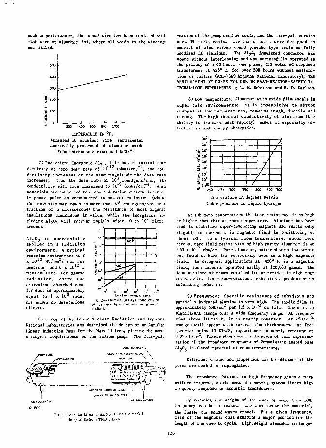
juch a performance, the round wire has baen replaced withflat wire or aluminum foil where all voids in the windingsare filled.
500
300
5 loo
• 200 tOO 600 BOO 1000
TEMPERATURE IN °F.Annealed EC aluminum wire, Pennalusteranodically processed of aluminum oxide
Film thickness 8 microns (.0003")
7) Radiation: Inorganic A^O-j film has in initial con-ductivity at zero dose rate of 10 (ohms/cm) , the con-ductivity increases at the same magnitude the dose rateincreases; thus the dose rate of 10 roentgens/sec., theconductivity will have increased to 10 (ohms/cm) . Whenmaterials are subjected to a short duration extreme intensi-ty gamma pulse as encountered in nuclear explosions (wherethe intensity may reach to more than 10 roentgens/sec. in afraction of a microsecond) the resistance of most organicinsulations diminishes in value, while the inorganics in-cluding A^Oo will recover rapidly after 10 to 100 micro-seconds.
AI2O3 is successfullyapplied in a radiationenvironment. A typicalreaction environment of 8x 10 1 2 NV/cm2/sec. for
12neutrons and 6 x 10 1mev/cm /sec. for gammaradiation, where theequivalent; absorbed dosefor each is approximatelyequal to 1 x 10 rads,has shown no deleteriouseffects.
flOOC
1 0 11 t 0 1 A
10 10 10 10 10 10"Dow Rati- Urnnlgcns Sen-nil
Fig. 2—Alumina CA12O;1) conductivityat various temperatures in gammaradiation.
In a report by Idaho Nuclear Radiation and ArgonneNational Laboratories was described the design of an AnnularLinear Induction Pump for the Mark 11 Loop, placing the moststringent requirements on the sodium pump. The four-pole
CORF HETAINER >
OIL COOLANT IN
! 12-862-1
Oil. COOLANT OUT
/
/
/
/
/
/
version of the pump used 24 co i l s , and the five-pole versionused 30 f i e l d c o i l s . The f i e l d c o i l s were designed toconsist of flat ribbon wound pancake type coils of fullyanodized EC aluminum. The AI2O3 insulated conductor waswound without interleaving and was successfully operated asthe primary of a 60 hertz, one phase, 230 volts AC stepdowntransformer at 425° C. for over 500 hours without malfunc-tion or failure (ANL-7369-Argonne National Laboratory), THEDEVELOPMENT OF PUMPS FOR USE IN FAST-REACTOR-SAFETY IN-TEGRAL-LOOP EXPERIMENTS by L. E. Robinson and R. D. Carlson.
8) Low Temperature: Aluminum with oxide film excels insuper cold environments; i t i s in sens i t i ve to abruptchanges at low temperatures, remains tough, duct i l e andstrong. The high thermal conductivity of aluminum (theability to transfer heat rapidly) makes i t especially ef-fective in high energy absorption.
10*
J 10'8 Itj6
Sio?, « *S109. l O 1 0
" 250 270 300 350 400 500 70C
Temperature in degrees KelvinUnder pressure in liquid hydrogen
At sub-zero temperatures the tear resistance i s as highor higher than that at room temperature. Aluminum has beenused to stabilize super-conducting magnets and reacts onlyslightly in increases in magnetic f ie ld in res is t iv i ty orabout 5KG. In a typical room temperature, under zerostress, zero field resist ivity of high purity aluminum is at2.53 + 10 ohm/cm. Pure aluminum, oxidized with low strainwas found to have low resist ivi ty even in a high magneticfield. In cryogenic applications at -450° F. in a magneticfield, such material operated easily at 120,000 gauss. Theless strained aluminum retained i t s properties in high mag-netic field. Its magno-resistance exhibited a predominatelysaturating behavior.
9) Frequency: Specif ic res is tance of anhydrous andpartially hydrated alumina is very high. The anodic film i sapproximately 5MQ/cm per 1.5 x 10 cm film. There is nosignificant change over a wide frequency range. At frequen-c i e s above lKHz/S R, i t i s nearly constant. At 25Q/cmchanges wi l l appear with varied film thicknesses. At fre-quencies below 10 KHz/S, capacitance i s nearly constant at0-99u F/cm . Figure shows some indication of fair represen-tation of the impedance component 01 Permaluster tested base
insulated material at room temperature.
T-ig. '.1. Annular Linear Induction Pump for Mark II
Integral Sodium TREAT Ldup
Different values and properties can be obtained if thepores are sealed or impregnated.
The impedance obtained in high frequency gives a nrreuniform response, as the mass of a moving system limits highfrequency response of acoustic transducers.
By reducing the weight of the mass by more than 50%,frequency can be increased. The more dense the material,the faster the sound waves travel. For a given frequency,mass of the magnetic coil exhibits a major portion for thelength of the wave to cycle. Lightweight aluminum rectangu-
126
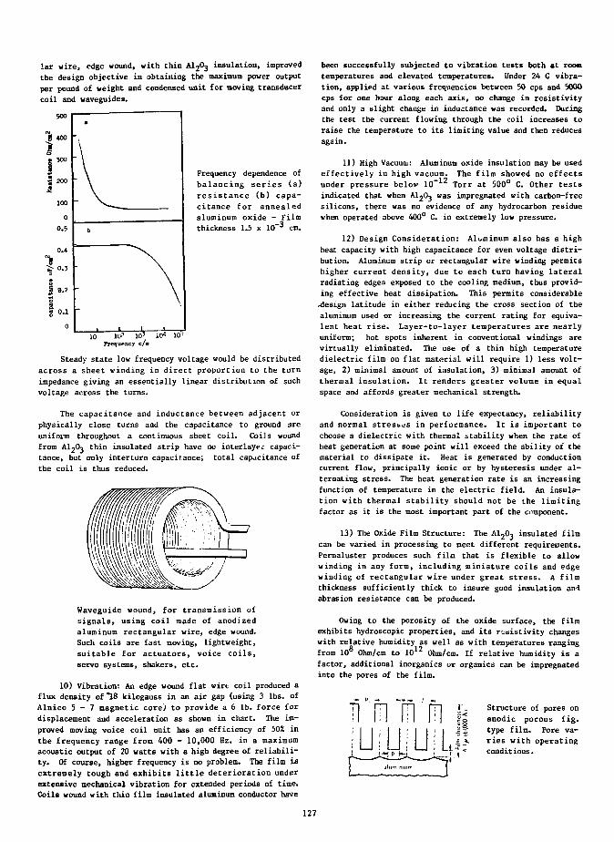
lar wire, edge wound, with thin A12O3 insulation, improvedthe design objective in obtaining the maximum power outputper pound of weight and condensed unit for moving transducercoil and waveguides.
frequency dependence ofbalancing s e r i e s (a)res i s tance (b) capa-citance for annealedaluminum oxide - Filmthickness 1.5 x 10 cm.
10 10' 10*frequency c/e
Steady state low frequency voltage would be distribuced
across a sheet winding in direct proportion to the turn
impedance giving an essentially linear distribution of such
voltage across the turns.
The capacitance and inductance between adjacent or
physically close turns and the capacitance to ground 3re
uniform throughout a continuous sheet coil. Coils wound
from A ^ O j thin insulated strip have no interlayer capaci-
tance, but only interturn capacif.ance; total capacitance of
the coil is thus reduced.
Waveguide wound, for transmission of
signals, using coil made of anodized
aluminum rectangular wire, edge wound.
Such coils are fast moving, lightweight,
suitable for actuators, voice coils,
servo systems, shakers, etc.
10) Vibration: An edge wound flat wire coil produced a
flux density of"18 kilogauss in an air gap (using 3 lbs. of
Alnico 5 - 7 magnetic core) to provide a 6 lb. force for
displacement and acceleration as shown in chart. The im-
proved moving voice coil emit has an efficiency of 50% in
the frequency range from 400 - 10,000 Hz. in a maximum
acoustic output of 20 watts with a high degree of reliabili-
ty. Of course, higher frequency is no problem. The film is
extremely tough and exhibits little deterioration under
extensive mechanical vibration for extended periods of time.
Coils wound with thin film insulated aluminum conductor have
been successfully subjected to vibration tests both at room
temperatures and elevated temperatures. Under 24 G vibra-
tion, applied at various frequencies between 50 cps and 5000
cps for one hour along each axis, no change in resistivity
and only a slight change in inductance was recorded. During
the test the current flowing through the coil increases to
raise the temperature to its limiting value and then reduces
again.
11) High Vacuum: Aluminum oxide insulation may be used
effectively in high vacuum. The film showed no effects
under pressure belov 10~ 1 2 Torr at 500° C. Other tests
indicated that when AljO^ was impregnated with carbon-free
silicons, there was no evidence of any hydrocarbon residue
when operated above 400° C. in extremely low pressure.
12) Design Consideration: Aluminum also has a high
heat capacity with high capacitance for even voltage distri-
bution. Aluminum strip or rectangular wire winding permits
higher current density, due to each turn having lateral
radiating edges exposed to the cooling medium, thus provid-
ing effective heat dissipation. This permits considerable
^design latitude in either reducing the cross section of the
aluminum used or increasing the current rating for equiva-
lent heat rise. Layer-to-layer temperatures are nearly
uniform; hot spots inherent in conventional windings are
virtually eliminated. The use of a thin high temperature
dielectric film on flat material will require 1) less volt-
age, 2) minimal amount of insulation, 3) minimal amount of
thermal insulation. It renders greater volume in equal
space and affords greater mechanical strength.
Consideration is given to life expectancy, reliability
and normal stresses in performance. It is important to
choose a dielectric with thermal stability when the rate of
heat generation at some point will exceed the ability of the
material to dissipate it. Heat is generated by conduction
current flow, principally ionic or by hysteresis under al-
ternating stress. The heat generation rate is an increasing
function of temperature in the electric field. An insula-
tion with thermal stability should not be the limiting
factor as it is the most important part of the component.
13) The Oxide Film Structure: The AljO-j insulated film
can be varied in processing to meet different requirements.
Pennaluster produces such film that is flexible to allow
winding in any form, including miniature coils and edge
winding of rectangular wire under great stress. A film
thickness sufficiently thick to insure good insulation an!
abrasion resistance can be produced.
Owing to the porosity of the oxide surface, the film
exhibits hydroscopic properties, and its resistivity changes
with relative humidity as well as with temperatures ranging
from 10 Ohm/cm to 10 Ohm/cm. If relative humidity is a
factor, additional inorganics or organics can be impregnated
into the pores of the film.
TI in ni m» • _ Structure of pores onanodic porous fig.type film. Pore va-ries with operatingconditions.
127
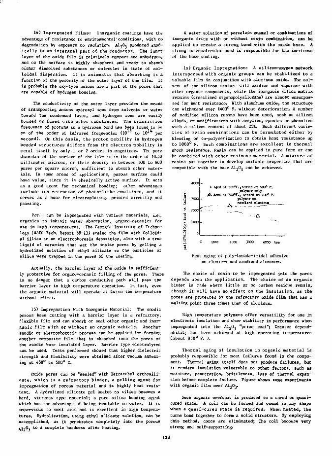
14) Impregnated Films: Inorganic coatings have the
advantage of resistance to environmental"conditions, with no
degradation by exposure to radiation. A ^ O j produced anod-
ically is an intergral part of the conductor. The inner
layer of the oxide film is relatively compact and anhydrous,
and on the surface is highly absorbent and ready to absorb
either dissolved substances or molecules in state of col-
loidal dispersion. It is axiomatic that absorbing is a
function of the porosity of the outer layer of the film. It
is probable the oxy-type anions are a part of the pores that
are capable of hydrogen bonding.
The conductivity of the outer layer provides the means
of transporting anions hydroxyl ions from solvents or water
toward the condensed layer, and hydrogen ions are easily
bonded or fused with other substances. The transistion
frequency of protons in a hydrogen bond has been found to be
on of the order of infrared frequencies (10 to 10 per
second). On this basis, the proton mobility in hydrogen
bonded structures differs from the electron mobility in
metal itself by only 1 or 2 orders in magnitude. The pore
diameter of the surface of the film is in the order of 10.50
millimeter microns, or their density is between 100 to 800
pores per square micron, sufficient to absorb other mater-
ials. In some areas of applications, porous surface could
have value, since it is chemically active surface. It acts
as a good agent for mechanical bonding; other advantages
include its retention of photo-litho emulsions, and it
serves as a base for electroplating, printed circuitry and
painting.
Port .; can be impregnated with various materials, i.e.,
organics to inhioit water absorption, organo-ceramics for
use in high temperatures. The Georgia Institute of Techno-
logy (WADC Tech. Report 58-13) sealed the film with Colloid-
al Silica in an electrophoresis deposition, also with a true
liquid of ceramics that wet the inside pores by gelling a
hydrolized solution of ethyl silicate so the particles of
silica were trapped in the pores of the coating.
Actually, the barrier layer of the oxide is sufficient-
ly protective for organo-ceramic filling of the pores. There
is no danger that a carbon conductive path will pass the
barrier layer in high temperature operation. In fact, even
the organic material will operate at twice the temperature
without effect.
15) Impregnation With Inorganic Material: The anodic
porous base coating with a barrier layer is a refractory,
flexible film and can absorb or seal other organic and inor-
ganic film with or without an organic vehicle. Another
anodic or eletrophoretic process can be applied for forming
another composite film that is absorbed into the pores of
the anodic base insulated layer. Barrier type electrolytes
can be used. Tests performed showed that higher dielectric
strength and flexibility were obtained after vacuum anneal-
ing at 450° to 500° C.
Oxide pores can be "sealed" with Tetraethyl orthosili-
cate, which is a refractory binder, a gelling agent for
impregnation of porous material and is highly heat resis-
tant. A hydrolized silicate gel heated to silica becomes a
hard, vitreous type material; a pure silica bonding agent
which has the advantage of being insoluble in water. It is
impervious to most acid and is excellent in high tempera-
tures. Hydrolization, using ethyl s'.licate solution, can be
accomplished, as it penetrates completely into the porous
Al2°3 t o a c o mP 1- e t e hardness after heating.
A water solution of porcelain enamel or combinations of
inorganic fritz with or without resin combination, can be
applied to create a strong bond with the oxide base, k
strong intermolecular bond is responsible for the inertness
of the base coating.
lo) Organic Impregnation: A silicon-oxygen network
interspersed with organic groups can be stabilized to a
valuable film in conjunction with aluminum oxide. The sol-
vent of the silicon mixture will oxidize and vaporize with
other organic components, while the inorganic silica matrix
remains (crosslined organopolysiloxans) are almost unsurpas-
sed lor heat resistance. With aluminum oxide, the structure
can withstand over 1400° F. without deterioration. A number
of modified silicon resins have been used, such as silicon
alkyds, or modifications with acrylics, epoxies or phenolics
with a silicon content of about 25%. Such different varie-
ties of resin combinations can be formulated either by
blending or co-polymerization to obtain heat resistance up
to 1000° F. Such combinations are excellent in thermal
shock resistance. Resin can be applied in pure form or can
be combined with other resinous material. A mixture of
resins put together to develop suitable properties that are
compatible with the base A^Oo can be achieved.
30O0
0 *g«i at 500°F.,tested at 500° F.polyBer only
[ at 70O°F., tested at 700° 7.polyner onanodlzed alumimv
A-o
Heat aging of poly-(amide-imide) adhesiveon alumiP'm and anodized aluminum.
The choice of resin to be impregnated into the poresdepends upon the application. The choice of an organicbinder is made where l i t t l e or no carbon residue remain,though i t wi l l have no effect on the insulat ion, as thepores are protected by the refractory oxide film that has amelting point three times that of aluminum.
High temperature polymers offer versatil i ty for use inelectronic insulation and show stability in performance whenimpregnated into the A^O^ "prime coat"; Greater depend-ability has been achieved at high operating temperatures(about 850° F. ).
Thermal aging of insulation in organic material isprobably responsible for most failures found in the compo-nent. Thermal aging itself does not produce failures, buti t renders insulation vulnerable to other factors, such asmoisture, penetration, brittleness, loss of thermal expan-sion before complete failure. Figure shows some experimentswith organic film over AI2O3.
Such organic overcoat is produced in a cured or quasi-cured state. A coil can be formed and wound in any shapewhen a quasi-cured s t a t e i s required. When heated, theturns bond together to form a solid structure. By enployingthis method, cores are eliminated; The coil becomes verystrong and self-supporting.
128
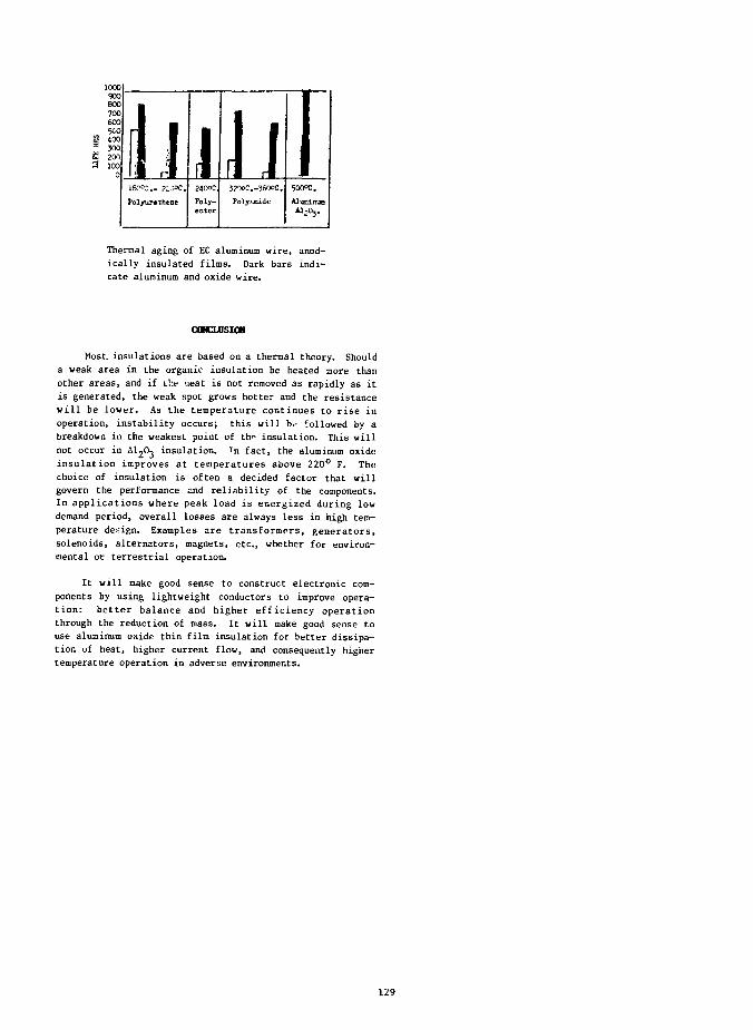
100090O80C700600500400300203100
0
m
1hPolyurethene
J240OC.
P o l y -ester
II3?ooC.-3600C.
Poly;jmide
•t1500°C.
Alualrair
Thermal aging of EC aluminum wire, anod-
ically insulated films. Dark bars indi-
cate aluminum and oxide wire.
CONCLUSION
Most, insulations are based on a thermal theory. Should
a weak area in the organic insulation be heated more than
other areas, and if ihe neat is not removed as rapidly as it
is generated, the weak spot grows hotter and the resistance
will be lower. As the temperature continues to rise in
operation, instability occurs; this will be followed by a
breakdown in the weakest point of thp insulation. This will
not occur in A^Oj insulation. T n fact, the aluminum oxide
insulation improves at temperatures above 220° F. The
choice of insulation is often a decided factor that will
govern the performance and reliability of the components.
In applications where peak load is energized during low
demand period, overall losses are always less in high tem-
perature design. Examples are transformers, generators,
solenoids, alternators, magnets, etc., whether for environ-
mental or terrestrial operation.
It will make good sense to construct electronic com-
ponents by using lightweight conductors to improve opera-
tion: better balance and higher efficiency operation
through the reduction of mass. It will make good sense to
use aluminum oxide thin film insulation for better dissipa-
tion uf heat, higher current flow, and consequently higher
temperature operation in adverse environments.
129
S E S S I O N V I
S P E C I A L K E Y N O T E A D D R E S S
A C O N F E R E N C E P E R S P E C T I V E
Technology Transfer and Commercialization of High Temperature Electronics
Dr. Robert PryGould, Inc.Rolling Meadows, Illinois
Dr. Robert Pry, Executive Vice President for R and D, Gould, Inc., has beeninvited to the conference to listen to the proceedings, have discussions with theauthors and attendees and from this background provide insights on the status ofeffort, interfaces between, and perception of the research, manufacturing anduser communities in high temperature electronics. The progress of R and D, fabrica-tion technology and commercialization of useful measurement systems at temperaturesgreater than 200°C will be assessed. The gaps between user needs, R and D resultsand on-going projects will be summarized yielding market expectations as projectedfrom user applications and manufacturer viewpoints. The apparent determinants forconimei *ialization of current research projects and the perceived interface barriersto technology transfer will be detailed.
For high temperature circuits, the areafrom the drain to the substrate junctionshould be as small as possible to decreasereverse leakage. This is accomplished by 9.horseshoeing the Z/Ls, thereby increasingcircuit density — this method is already incommon use.
To make high-temperature circuits more 10.reliable, metal lines should be as broad anddeep as possible, again sacrificing chip area.
Conclusions 11.
Existing CMOS technology can be used toproduce stable and useful circuits that oper-ate at 300°C for 1000 hours. This accomplish-ment, however, sacrifices some chip area anddoes not provide gate protection. For this 12.latter problem, high-temperature GaAs andGaP diodes should be developed as protectiondevices. Although these diodes would probablybe outside the CMOS chip, they could be partof the same flat pack. 13.
Dielectric isolation CMOS would be agreat improvement over junction isolation andwork has begun in this area. New solar celldiodes show promise as input protectiondevices. This would allow us to be completelyintegrated again.
Surfaces," IEEE Transactions ElectronDevices, 248, May 1965.
F. N. Schrieffer, Effective CarrierMobility in Surface-Space ChargeLayers," Phys. Review, 97, pp. 641,1955.
W. M. Bullis, "Properties of Gold inSilicon," Solid-state Electronics, 9pp. 143, 1966.
B. E. Deal, et al., "Characteristicsof the Surface State charge (Qss) ofThermally Oxidized Silicon,"Electrochemical Society, 144, pp. 266,1967.
C. W. White, J. Narayans, and R. T.Young, "Laser Annealing of Ion-Implanted Semiconductors," Science,204 (4382):461, May 1979.
J. D. McBrayer, "High-TearperatureComplementary Metal Oxide Semicon-ductors (CMOS)," Sandia NationalLaboratories, SAND79-1487, October1979.
References
1. J. L. Prince of Clemson University,Investigation of the Performance ofSemiconductor Devices at ElevatedTemperatures, Sandia NationalLaboratories, under Contract No.06-4336, November 1977.
2. D. W. Palmer, B. L. Draper, J. D.McBrayer, and K. R. White, "ActiveDevices for High-TemperatureMicrocircuitry," Sandia NationalLaboratories, SAND77-1145, February1978.
3. B. L. Draper and D. W. Palmer,"Extension of High-TemperatureElectronics," Proceedings of ECC,1979.
4. J. D. McBrayer, "CMOS Test Chips,"Sandia National Laboratories,SAND78-1390, August 1978.
5. A. S. Grove, Physics and Technologyof Semiconductor Devices^ (New York,John Wiley « Sons, Inc.,) 1967.
6. S. M. Sze, Physics of SemiconductorDevices, (New York, Wiley-Interscience)
7. W. M. -Penney and L. Lau, MOSIntegrated Circuits, (New York,Van Nostrand Reinhold Co.) 1972.
8. 0. Leistiko, Jr., A. S. Grove,and C. T. Sah, "Electron andHole Mobilities in Inversion Layerson Thermally Oxidized Silicon
104
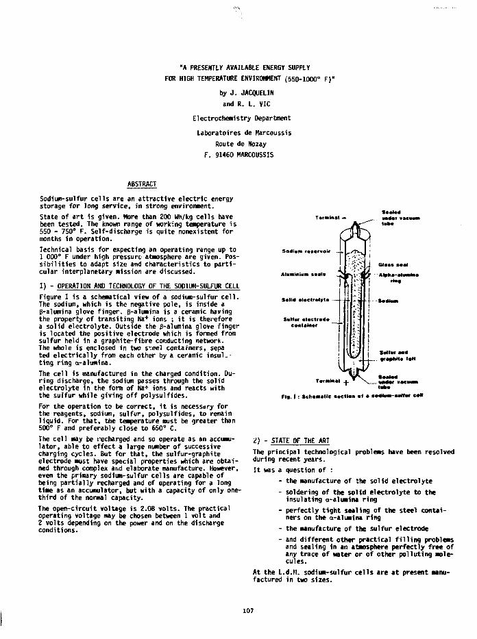
"A PRESENTLY AVAILABLE ENERGY SUPPLYFOR HIGH TEMPERATURE ENVIRONMENT (550-1000°
by J. JACQUELINand R. L. VIC
Electrochemistry Department
Laboratoires de HarcoussisRoute de Nozay
F. 91460 HARCOUSSIS
F)"
ABSTRACT
Sodium-sulfur ce l l s are an at t ract ive e lect r ic energystorage for long service, in strong environment.
State of a r t is given. More than 200 Wh/kg ce l ls havebeen tested. The known range of working temperature is550 - 750° F. Self-discharge is quite nonexistent formonths in operation.
Technical basis for expecting an operating range up to1 000" F under high pressure atmosphere are given. Pos-s i b i l i t i e s to adapt size and characteristics to p a r t i -cular interplanetary mission are discussed.
1) - OPERATION AND TECHNOLOGY OF THE SODIUM-SULFUR CELL
Figure 1 is a schematical view of a sodium-sulfur c e l l .The sodium, which is the negative pole, is inside ag-alumina glove f inger. 6-alumina is a ceramic havingthe property of t ransi t ing Na+ ions ; i t is thereforea solid e lect ro ly te . Outside the S-alumina glove f ingeris located the positive electrode which is formed fromsulfur held in a graphite- f ibre conducting network.The whole is enclosed in two steel containers, sepated e l e c t r i c a l l y from each other by a ceramic i n s u l -t ing ring a-alumina.
The ce l l is manufactured in the charged condition. Du-ring discharge, the sodium passes through the solidelectrolyte in the form of Na+ ions and reacts withthe sulfur while giving o f f polysulfides.
For the operation to be correct, i t is necessary forthe reagents, sodium, sul fur , polysulfides, to remainl i q u i d . For tha t , the temperature must be greater than500° F and preferably close to 650° C.
The cel l may be recharged and so operate as an accumu-l a t o r , able to ef fect a large number of successivecharging cycles. But for tha t , the sulfur-graphiteelectrode must have special properties which are obta i -ned through complex and elaborate manufacture. However,even the primary sodium-sulfur ce l ls are capable ofbeing p a r t i a l l y recharged and of operating for a longtime as an accumulator, but with a capacity of only one-th i rd of the normal capacity.
The open-circuit voltage is 2.08 vo l ts . The practicaloperating voltage may be chosen between 1 volt and2 volts depending on the power and on the dischargeconditions-
um reservoir
Soli* «l«ctrolyt«
Sutler electrodecontainer
Terminal
Fit - 1 : Schematic section ef a »e«l>m-e««f can
2) - STATE OF THE ART
The principal technological problems have been resolvedduring recent years.
I t was a question of :
- the manufacture of the solid electrolyte
- soldering of the solid electrolyte to theinsulating a-alumina ring
- perfectly tight sealing of the steel contai-ners on the a-alumina ring
- the manufacture of the sulfur electrode
- and different other practical f i l l ing problemsand sealing in an atmosphere perfectly free ofany trace of water or of other polluting mole-cules.
At the L.d.M. sodium-sulfur cells are at present manu-factured in two sizes.
107
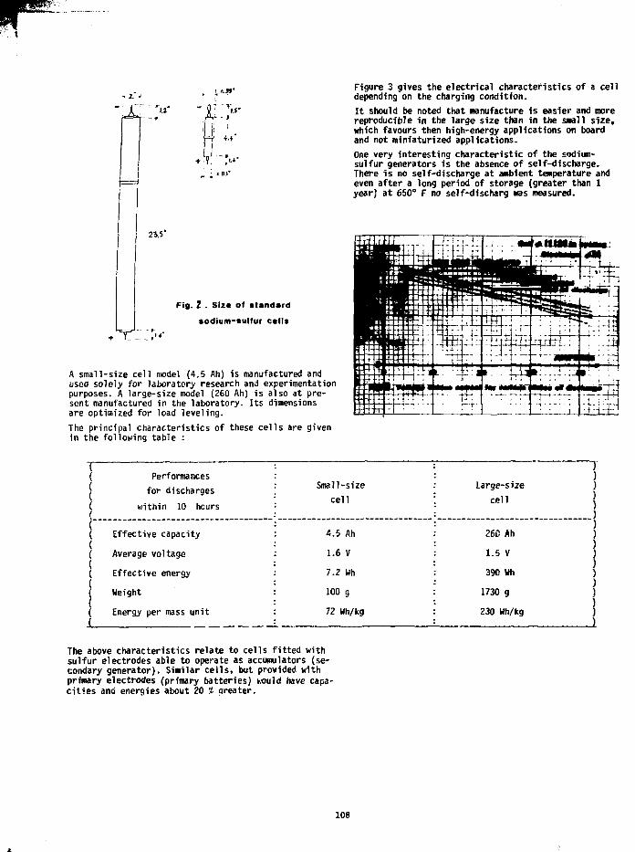
X-,'"'
2J.5"
Fig. 2 . Siz* of standard
sodium-sulfur calls
A small-size cell model (4.5 Ah) is manufactured andused solely for laboratory research and experimentationpurposes. A large-size model (260 Ah) is also at pre-sent manufactured in the laboratory. I t s dimensionsare optimized for load leveling.
The principal characteristics of these cel ls are givenin the following table :
Figure 3 gives the electrical characteristics of a celldepending on the charging condition.I t should be noted that manufacture is easier and morereproducible in the large size than in the small size,which favours then high-energy applications on boardand not miniaturized applications.
One very interesting characteristic of the sodium-sulfur generators is the absence of self-discharge.There is no self-discharge at ambient temperature andeven after a long period of storage (greater than 1year) at 650° F no self-discharg was measured.
Performancesfor discharges
within 10 hours
Small-size
cell
Large-size
cell
Effective capacity
Average voltage
Effective energy
Weight
Energy per mass unit
4.5 Ah
1.6 V
7.2 Wh
100 g
72 Wh/kg
260 Ah
1.5 V
390 Wh
1730 g
230 Wh/kg
The above characteristics relate to cells fitted withsulfur electrodes able to operate as accumulators (se-condary generator). Similar cells, but provided withprimary electrodes (primary batteries) would have capa-cities and energies about 20 % greater.
108
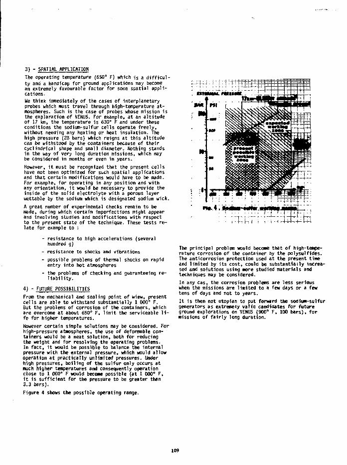
3) - SPATIAL APPLICATION
The operating temperature {650° F) which is a difficul-ty and a handicap for ground applications may becomean extremely favourable factor for some spatial appli-cations-We think immediately of the cases of interplanetaryprobes which must travel through high-temperature at-mospheres. Such is the case of probes whose mission isthe explaration of VENUS. For example, at an altitudeof 17 km, the temperature is 630° F and under theseconditions the sodium-sulfur cells operate freely,without needing any heating or heat insulation. Thehigh pressure (28 bars) which reigns at this altitudecan be withstood by the containers because of theircyciindrical shape and small diameter. Nothing standsin the way of very long duration missions, which maybe considered in months or even in years.
However, it must be recognized that the present cellshave not been optimized for such spatial applicationsand that certain modifications would have to be made.For example, for operating in any position and withany orientation, it would be necessary to provide theinside of the solid electrolyte with a porous layerwettable by the sodium which is designated sodium wick.
A great number of experimental checks remain to bemade, during which certain imperfections might appearand involving studies and modifications with respectto the present state of the technique. These tests re-late for example to :
- resistance to high accelerations (severalhundred g)
- resistance to shocks and vibrations
- possible problems of thermal shocks on rapidentry into hot atmospheres
- the problems of checking and guaranteeing re-liability.
4) - FUTURE POSSIBILITIES
From the mechanical and sealing point of wiew, presentcells are able to withstand substantially 1 000° F.But the problems of corrosion of the containers, whichare overcome at about 650° F, limit the serviceable li-fe for higher temperatures.
However certain simple solutions may be considered. Forhigh-pressure atmospheres, the use of deformable con-tainers would be a neat solution, both for reducingthe weight and for resolving the operating problems.In fact, it would be possible to balance the internalpressure with the external pressure, which would allowoperation at practically unlimited pressures. Underhigh pressures, boiling of the sulfur only occurs atmuch higher temperatures and consequently operationclose to 1 000° F would become possible (at 1 000° F,it is sufficient for the pressure to be greater than3.3 bars).
Figure 4 shows the possible operating range.
::U~i : i' I • - ^ n ^ - t r f T t r t z t
Mft
The principal problem would become that of high-tempe-rature corrosion of the container by the polysulfides.The anticorrosion protection used at the present timeand limited by its cost, could be substantially increa-sed and solutions using more studied materials andtechniques may be considered.
In any cas, the corrosion problems are less seriouswhen the missions are limited to a few days or a fewtens of days and not to years.
It is then not Utopian to put forward the sodium-sulfurgenerators as extremely valid candidates for futureground explorations on VENUS {900° F, 100 bars), formissions of fairly long duration.
109
wo
STUFFED MO LAYER AS A DIFFUSION BARRIER IN METALLIZATIONS FOR HIGH TEMPERATURE ELECTRONICS
John K. Boah, General Electric Company, EP-7, Syracuse, New York, 13221
Virginia Russell, General Electric Company, EP-3, Syracuse, New York, 13221
David P. Smith, General Electric Company, EP-7, Syracuse, New York, 13221
Abstract
Auger electron spectroscopy (AES) was employed tocharacterize the diffusion barrier properties ofmolybdenum in the CrSi2/Mo/Au metallization system.The barrier action of Mo was demonstrated to persisteven after 2000 hours annealing time at 300cC in anitrogen ambient.
At 340°C annealing temperature, however, rapidinterdiffusion was observed to have occurred betweenthe various metal layers after only 261 hours.
At 450°C, the metallization degraded after onlytwo hours of annealing.
The presence of controlled amounts of oxygen in theMo layer is believed to be responsible for suppressingthe short circuit interdiffusion between the thinfilm layers. Above 340°C, i t is believed that theincrease in the oxygen mobility led to deteriorationof i ts stuffing action, resulting in the rapidinterdiffusion of the thin film layers along grainboundaries.
The CrSi2/Mo/Au barrier metallization system lentitself easily to fine line patterning.
Introduction
Thin film metallizations play a critical role in therel iabi l i ty of microelectronic devices. Thedeleterious effects of aluminum alloy penetration'"2and the "purple plague"3-4 in gold-aluminum thinfilm couples are well-known examples. Thin filmmetallizations are made up of very small grains,high densities of grain boundaries and dislocations.I t is well established that grain boundaries anddislocations increase atomic mobility by acting asshort circuit diffusion paths.5"6. Gjostein6 hasshown that for face centered cubic metals, thin filminterdiffusion is controlled by dislocation pipediffusion and grain boundary diffusion in thetemperature range 30-60 percent of the meltingpoint. Below this temperature range, interdiffusionis not very significant. Above this temperaturerange, lattice diffusion predominates. Diffusionbarriers? such as stuffed barriers, passive barriers,sacrificial barriers and thermodynamically stablebarriers, are intended to suppress short circuitcontrolled interdiffusion. The purple plaguementioned earlier can be ascribed to Kirkendallvoiding through short circuit interdiffusion.
Harris et al8 reported that the diffusion of Ti in Mowas inhibited by the presence of oxygen in the Molayer of a Ti/Mo/Au system. Nowicki and Wangy
observed the suppression of Au-Si intermixing inSi/Mo/Au system i f the Mo layer was reactivelysputtered in N2-Ar mixture. They attributed theenhanced Mo barrier action to N2 occupation of theoctahedral sites around the Mo atoms. Neither ofthe above studies dealt with prolonged annealingeffects at high temperatures.
The need for high temperature (up to 300°C) micro-electronics applications in such diverse fields asaircraft engine controls, nuclear reactor o remonitoring instrumentation and oil and gas welldownhole instrumentation has further imposedstringent rel iabi l i ty requirements on microelectronicinterconnections. Diffusion barrier protection ofthe ohmic contact layer and metal conductor ''aver thusassumes new importance. This paper will discuss theenhanced high temperature diffusion barrier propertiesachieved through the introduction of controlledamounts of oxygen in the Mo barrier layer of theCr/Mo/Au metallization system.
A barrier metallization system is shown schematicallyin Figure 1. I t consists of an ohmic contact layer(CrSi2), a diffusion barrier layer (stuffed Mo) and aninterconnect or conductor layer (Au). Figure 2illustrates a tri-metal system where diffusion barrierprotection is lost during heat treatment.
Experimental Procedure
Sequential deposition of the thin film layers of Cr,Mo, and Au on (111)-oriented, N-type silicon singlecrystal wafers was carried out using planar r.f.magnetron sputtering (Perkin-Elmer Ultec Model 2400-8SA). Sputtering pressures were less than 10 mtorrusing argon. Oxygen-argon gas mixtures were utilizedfor reactive sputtering of the Mo. Prior to sputtering,the silicon wafers were etched in dilute HF, rinsedthoroughly in de-ionized water, air dried and trans-ferred immediately into the sputtering chamber.
After sequentially depositing the Cr/Mo/Au system,sintering was performed in a quartz tube in a flowingnitrogen ambient at 450°C for 15 minutes to affectCrSi2 formation.
Annealing experiments were subsequently carried outat 300°C, 340°C and 450°C. The 300°C anneals wereperformed in nitrogen ambients in a quartz tube for168 hours, 1000 hours and 2000 hours.
Annealing experiments above 300°C were carried out invacuum. AES was employed to study the extent of thinfilm interdiffusion between the various metal layers.Fine line pattern definition was evaluated using acombination of photolithographic and chemical etchingtechniques.
Results and Discussions
AES profiles of the Cr/Mo/Au system before and aftersintering at 300°C are shown in Figures 3-6. Therewas limited penetration of the Cr layer by the Mo layerduring the sputter deposition. After annealing at300°C for 2000 hours, the diffusion barrier propertiesof the Mo layer were found to be intact. Some re-distribution of the oxygen in the Mo layer occurredduring the 300°C annealing. The suppression of theexpected grain boundary interdiffusion may be
i l l
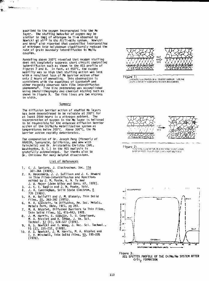
m
ascribed to the oxygen incorporated into the Holayer. The stuff ing behavior of oxygen may besimilar to that of nitrogen in Ti-W observed byNowicki et a l 1 0 in the Al/Ti-W/Au system. Nowickiand Wang9 also reported that controlled incorporationof nitrogen into molybdenum signif icant ly reduced therate of grain boundary interdiffusion in Mo/Aucouples.
Annealing above 300°C revealed that oxygen stuff ingdoes not completely suppress short c i r cu i t controlledinterdif fusion such as shown in the AES prof i le ofFigures 7 and 8. In fact , at 450°C, the oxygenmobil i ty was so high that stuff ing action was lostwith a resultant loss of Mo barrier action afteronly 2 hours of annealing. This observation isconsistent with the equations of Gjostein^ andother recently observed thin f i lm interdiffusionphenomena . Fine l ine patterning was accomplishedusing photolithography and chemical etching such asshown in Figure 9. The fine lines are two micronsin width.
V .' • ' r /,*;/,'./ TIME\, :/-J V / Y ,< / A ,
V
Figure 1:' JCHLMATIC HlUiTRAMON OF A "STUFFED"BARRIER. XOTE tHE
(.AStniiS r.'.PURIlv SEGREGATES TO GRAIN BO1ADARIES.
The diffusion barrier action of stuffed Mo layershas been demonstrated to be rel iable at 300°C forat least 2000 hours in a nitrogen ambient. Theincorporation of oxygen in the Ho layer is believedto be responsible for the enhanced diffusion barrieraction of the Cr/Mo/Au metallization system attemperatures below 300°C. Above 300°C, the Mobarrier action rapidly deteriorates.
The cooperation of Dr. Joseph Peng (formerly ofARACOR, Sunnyvale, California, and now withFairchild) and Dr. Ar is tote l is Christou (NRL,Washington, D. C.) in the AES analysis isgrateful ly acknowledged. Our thanks also toDr. Christou for many helpful disucssions.
List of References
1. C. J . Santoro, J. Electrochem. Soc. ]}6361-364 (1969).
2. R. Rosenberg, J. J . Sullivan and J. K. Howardin Thin Films-Interdiffusion and Reactionsedited by J. M. Poate, K. N. Tu andJ. W. Mayer (John Wiley and Sons, NV, 1978).
3. J . E. E. Baglin and J. M. Poate, ib id .4. J . A. Cunningham, Solid State Electron, 8
735 (1965).5. R. W. Bal lu f f i and J. M. Blakely, Thin Solid
Films, 25_, 363-392 (1975).6. N. A. Gjostein, in Diffusion, Am. Soc. Metals,
Metals Park, Ohio, 1973, pg 241.7. M. A. Nicolet, Diffusion Barriers in Thin Films,
Thin Solid Films, 52., 415-443, 1978.8. J . H. Harris, E. Lugujjo, S. U. Campisano,
M. A. Nicolet and R. Shima, J . Va. Sci.Technol. 12 (1) , 524-527 (1978).
9. R. S. NowTcki and I . Wang, J . Vac. Sci. Technol.15 (2) , 235-237, (1978).
10. R. S. Nowicki, J . M. Harris, M. A. Nicolet andI . V. Mitchel l , Thin Solid Films, 53_, 195-205(1978).
hiAi= =IlV.t
^mFigure 2:
^l-e. 'AIIC ILIUSWMO>. C« A IRI-MEIAL SVSTiVi .-.MfOBASSIiR PROTiLJIO*. IS 1OST OURI'.GHEAI TRl*T"[ ' . I
AS EtfAPQRA'ED
s i ; f
. 1 '•
Figure 3:AES SPUTTER PROFILE OF THE Cr/Mo/Au SYSTEM AFTER
CrSi2 FORMATION
112
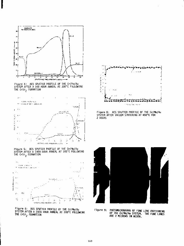
I11
PE
AK
0
80
70
60
50
40
30
20
10
166
Aul?
°i—
ANNEALEDHOURS AT 300 C
,
. (
\i
/2 4
/
OXYGEN . 1
6 " 9 " 10
5PUTTERING TIME |AR
/
/
12 M
BITRARY UNITS'
i(1lll\
vA16
. w
u..111111I1 ...
Jl—
1 l.. n. .18 V 22
Figure 4: AES SPUTTER PROFILE OF THE Cr/Ko/AuSYSTEM AFTER A 168 HOUR ANNEAL AT 300°C FOLLOWINGTHE CrSi2 FORMATION
SI'.tEPI'.f. II1.'!
Figure 5: AES SPUTTER PROFILE OF THE Cr/Mo/AuSYSTEM AFTER A 1000 HOUR ANNEAL AT 300°C FOLLOWINGTHE CrSi FORMATION
Si:.U«fi\tt|v.t ^
• i1' t
ji TJ 2t
Figure 6: AES SPUTTER PROFILE OF THE Cr/Mo/AuSYSTEM AFTER A 2000 HOUR ANNEAL AT 300cC FOLLOWING
Figure 8: AES SPUTTER PROFILE OF THE Cr/Ho/AuSYSTEM AFTER VACUUM SINTERING AT 450°C FOR2 HOURS
THE CrSi2 FORMATIONFigure 9: PHOTOMICROGRAPH OF FINE LINE PATTERNING
OF THE Cr/Mo/Au SYSTEM. THE FINE LINESARE 2 MICRONS IN WIDTH.
113
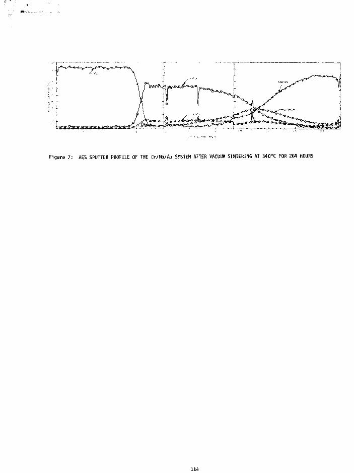
Figure 7: AES SPUTTER PROFILE OF THE Cr/Mo/Au SYSTEM AFTER VACUUM SINTERING AT 34O°C FOR 264 HOURS
114
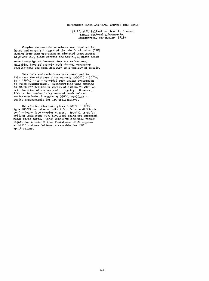
REFRACTORY GLASS AND GLASS CERAMIC TUBE SEALS
Clifford P. BalXard and Donn L. StewartSandia National Laboratories
Albuquerque, New Mexico 87185
Complex vacuum tube envelopes are required tohouse and support integrated thermionic circuits (ITC)during long-term operation at elevated temperatures.Li20-Zn0-Si02 glass ceramic and CaO-Al2O3 glass seals
were investigated because they are refractory,moldable, have relatively high thermal expansioncoefficients and bond directly to a variety of metals.
Materials and techniques were developed tofabricate the silicate glass ceramic (p500°C = 10 QffliTg = 450°C) into a toroidal tube design containing64 Pt/Rh feedthroughs. Subassemblies were exposedto 600°C for periods in excess of 140 hours with nodeterioration of vacuum seal integrity. However,lithium ion conductivity reduced lead-to-leadresistance below 1 megohm at 350°C, yielding adevice unacceptable for ITC applications.
q
The calcium aluminate glass (p500°C = 10 fim;Tg = 900°C) contains no alkali but is more difficultto fabricate into complex shapes. Special transfermolding techniques were developed using pre-enameledmetal piece parts. These subassemblies were vacuumtight, had a lead-to-lead resistance of 20 ciegohmsat 600°C and are believed acceptable for ITCapplications.
115
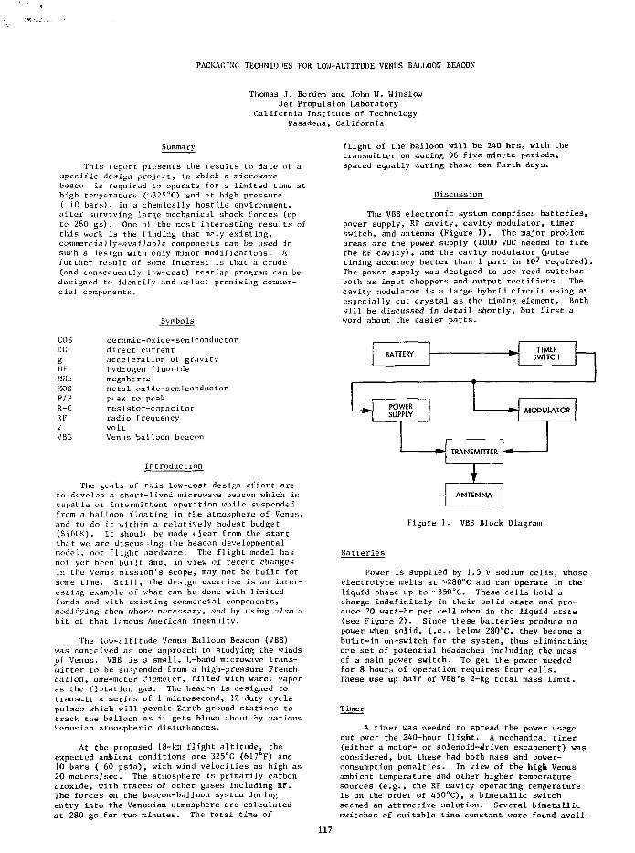
PACKAGING TECHNIQUES FOR LOW-ALTITUDE VENUS BALLOON BEACON
Thomas J. Border) and John U. WinslowJet Propulsion Laboratory
California Institute of TechnologyPasadena, California
Summary
This report presents the results to date of aspecific design project, in which a microwavebeaco is required to operate for a limited time athigh temperature (' '325OC) and at high pressure( 10 bars), in a chemically hostile environment,after surviving large mechanical shock forces (upto 280 gs). One of the most interesting results ofthis work is the finding that mr-.y existing,commerciaJly-available components can be used insuch a -iesign with only minor modifications. Afurther result of some interest is that a crude(and consequently Iw-cost) testing program can bedesigned to identify and select promising commer-cial components.
COS ceramic-oxide-semiconductorDC direct currentg acceleration of gravityHF hydrogen fluorideMHz megahertzHOS metal-oxide-semiconductorP/P peak to peakR-C resistor-capacitorRF radio frequencyV voltVBB Venus balloon beacon
Introduction
The goals of this low-cost design effort areto develop a short-lived microwave beacon which iscapable of intermittent opention while suspendedfrom a balloon floating in the atmosphere of Venus,and to do it within a relatively modest budget($160K). It shoult be made clear from the startthat we are discussing the beacon developmentalmodel , not flight .lardware. The flight model hasnot yet been built and, in view of recent changesin the Venus mission's scope, may not be built forsome time. Still, the design exercise is an inter-esting example oi v/hat can be done with limitedfunds and vith existing commercial components,modifying them where necessary, and by using also abit of that famous American ingenuity.
The low-altituclwas conceived as oneoi Venus. VBB is ai.iitter to be suspendballon, one-meter Jias the f1 station gastransmit a series ofpulses which will petrack the balloon asVenusian atmospheric
e Venus Balloon Beacon (VBB)approach to studying the windssmall, L-band microwave trans-ed from a high-pressure FrenchT.ciec, tilled with watet vaporThe beacon is designed to
1 microsecond, 1Z duty cyclermit Earth ground stations toi: gets blown about by variousdisturbances.
At the proposed 18-km flight altitude, theexpected ambient conditions are 325°C (617°F) and10 bars (160 psia), with wind velocities as high as20 meters/sec. The atmosphere is primarily carbondioxide, with traces of other gases including HF.The forces on the beacon-balloon system duringentry into the Venusian atmosphere are calculatedat 280 gs for two minutes. The total time of
flight of the balloon will be 240 hrs: with thetransmitter on during 96 five-minute periods,spaced equally during those ten Earth days.
Discussion
The VBB electronic system comprises batteries,power supply, RF cavity, cavity modulator, timerswitch, and antenna (Figure 1). The major problemareas are the power supply (1000 VDC needed to firethe RF cavity), and the cavity modulator (pulsetiming accuracy better than 1 part in 10? required).The power supply was designed to use reed switchesboth as input choppers and output rectifiers. Thecavity modulator is a large hybrid circuit using anespecially cut crystal as the timing element. Bothwill be discussed in detail shortly, but first aword about the easier parts.
BATTERY
POWERSUPPLY
TRANS
TIMERSWITCH
MODULATOR
ANTENNA
Figure 1. VBB Block Diagram
Batteries
Power is supplied by 1.5 V sodium cells, whoseelectrolyte melts at " 280°C and can operate in theliquid phase up to "<350cC. These cells hold acharge indefinitely in their solid state and pro-duce 20 wat£-hr per cell when in the liquid state(see Figure 2). Since these batteries produce nopower when solid, i.e., below 28O°C, they become abuiit-in on-switch for the system, thus eliminatingore set of potential headaches including the massof a main power switch. To get the power neededfor 8 hours of operation requires four cells.These use up half of VBB's 2-kg total mass limit.
Timer
A timer was needed to spread the power usageout over the 240-hour flight. A mechanical timer(either a motor- or solenoid-driven escapement) wasconsidered, but these had both mass and power-consumption penalties. In view of the high Venusambient temperature and other higher temperaturesources (e.g., the RF cavity operating temperatureis on the order of 450°C), a bimetallic switchseemed an attractive solution. Several bimetallicswitches of suitable time constant were found avail-
117
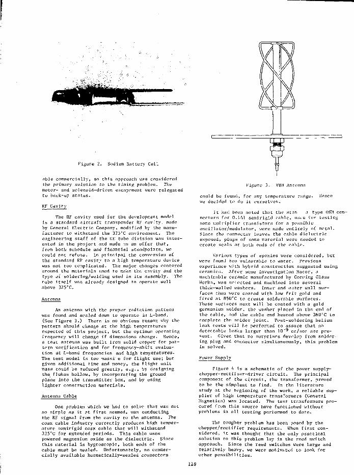
Figure 2. Sodium Battery Cell
able commercially, so this approach was consideredthe primary solution to the timing problem. Themotor- and solenoid-driven escapement were relegatedto back-up status.
The RF cavity used for the development modelis a standard aircraft transponder RF cavity, madeby General Electric Company, modified by the manu-facturer to withstand the 325°C environment. Theengineering staff of the GE tube division was inter-ested in the project and made us an offer that,from both schedule and financial standpoints, wecould not refuse. In principal the conversion ofthe standard RF cavity to a high temperature devicewas not too complicated. The major changes centeredaround the materials used to make the cavity and thetype of soldering/welding used in its assembly. Thetube itself was already designed to operate wellabove 325°C.
Antenna
An antenna with the proper radiation patternwas found and scaled dow to operate in L-band.(See Figure 3.) There is no obvious reason why thepattern should change at the high temperaturesexpected of this project, but the optimum operatingfrequency will change if dimensions change. Hence,a test antenna was built from solid copper for pat-tern verification and for frequency-shift evalua-tion at L-band frequencies and high temperatures.The test model is too massi e for flight use; butgiven additional time and money, the flight unitmass could be reduced greatly, e.g., by designingthe flukes hollow, by incorporating the groundplane into the transmitter box, and by usinglighter construction materials.
Antenna Cable
One problem which we had to solve that was notso simple as it .t first seemed, was conductingthe RF signal from the cavity to the antenna. Thecoax cable industry currently produces high temper-ature semirigid coax cable that will withstand325°C for extended periods. This cable usespowered magnesium oxide as the dielectric. Sincethis material is hygroscopic, both ends of thecable must be sealed. Unfortunately, no commer-cially available hermetically-sealed connectors
Figure 3. VBB Antenna
could be found, for any temperature range. Hencewe decided to do it ourselves.
It had been noted that the star. j type OSM con-nectors for 0.141 semirigid cable, u.-u a for testingsome multiplier transistors for a possibleoscillator/modulator, were made entirely of metal.Since the connector leaver the cable dielectricexposed, plugs of some iraterial were needed tocreate seals at both ends of the cable.
Various types of epoxies were considered, butwere founJ too vulnerable to water. Previousexperience w.'th hybrid construction suggested usingceramics. After some investigation Macor, amachinable ceramic manufactured by Corning GlassWorks, was seJected and machined into severalthick-walled washers. Inner and outer wall sur-faces then were coated with low frit gold andfired at 850°C to create solderable surfaces.These surfaces next will be coated with a goldgermanium solder, the washer placed in the end ofthe cable, and the cable end heated above 360"C tocomplete the solder joint. Post-soldering heliumleak tests will be performed to assure that nodetectable leaks larger than 10"^ cc/sec are pre-sent. Given that no surprises develop from solder-ing plug and connector simultaneously, this problemis solved.
Figure 4 is a schematic of the poxjer supply-chopper-rectifler-driver circuit. The principalcomponent of the circuit, the transformer, provedto be the simplest to find. In the literaturestudy at Che beginning of the work, a reliable sup-plier of high temperature transformers (GeneralMagnetics) was located. The test transformers pro-cured from this source have functioned withoutproblems in all testing performed to date.
The tougher problem has been, posed by thechopper/rectifier requirements. When first con-sidered, it was thought that the only practicalsolution to this problem lay in the reed switchapproach. Since the reed switches were large andrelatively heavy, we were motivated to look forother possibilities.
118
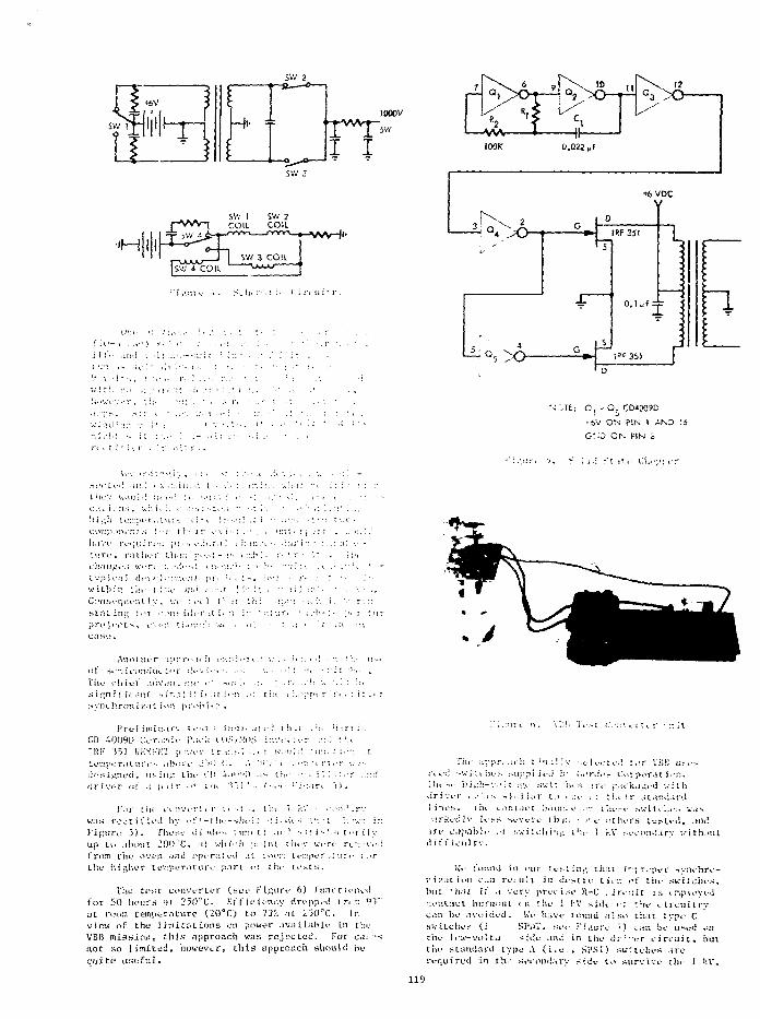
SV/ 1 T1000 V
i i
SW I SV/ 2
COIL COIL
f i t ' - i • T V ' r . • ! • . • :
i i i ' . , i n . | v . . i : ! . • . , - . - , ' .
t v . . l - - . , ; - . - , . ! • . • :
w i t ( . i i . ' i ; ;• i i • • • : ' • ! •
ri ' • : : : • . r . •": .: i'. r-
I00K
• H IKF35I
O.Ufi
35!
NOTE: G , - Q . C0400?C
•6V ON PIN 1 ANO 14
G'.O ON PIN i
». . '• '•li-.: : ' ; ili> l ' . h i ip ;v r
s i v l i ' i l i i ! J . : - . . ; r . i n . < f . I . • .'.- : j : \ - 5 : . > . • : • : • , - . : : • : •••
I ; K - v v ; a i i i ^ ; ; < < • • : : . - . ' : ! . ; . < ; . . ' i ^ : . ' • « <, - . : -
h i . . ; : : U ' ^ ' p i r . ' . H i r v v : : r i i : i , : : ' , : i -• < • : • ' . •'_••: : : A ' •
e o v . ' . p . i r i t T . L . s I ' T t h - i r i 1 - . f -. I L : • — u : : : * : , ; : ? , : . < - : M
i l - i \ p i ' r i - ' j i : ; V t d ; i : ' • i . . . . : i . r . i ! ( i : , i : : . - i : . ' . i r i ; 1 : . : : : i : i -
c u r i . * , r a t i i . . - : ' t - i i ! ; ; ; : > ' . - . ; - ;•* . < : : J M - ; • . t : • i : . i h i
c h . n i ^ i - s i ' . v r i ' : . . ' ^ > - - l i : v • - . • ' ! : > ' • - : ; ; : : i i L - . r
, • "
L y p i i - . - i ! d i ' V f ! ; - ; n n - : i l | ' r . . : . i : - . ' • • • ! -•- :'• : : • •
w ! . L l l i v . L h f I J : : : i ' . * : ; J < • - t ! : ' ! : - c : ; ; : : ' • ' : i . - r
C c i n « ^ q i H ' V > l I ; ; . ' . v i : r i ! I ' - . j t : ! : : : . , : • ; - - . i ; ! . • : : : : !
s t ; l t i n g N T i v i - s i i v r a : . ' . : i : ' - : : : ' . : v . • . . ' I ; - : . : ; > . ; • . : u :
p r o j ' ' i 1 L > , , < - v i ' : ' . t i i i u r . - ' n v . . ' M ' - • • : ; ; •• : ; n \ " i i
C I S ' . ' .
A n o t m - r i p p i * " i ' i i v . : : ' \ ••:'•:' ' . • . ' : • ' » : . • ! • : ! " : » i : - > .
o f s i - - n V i > m I n < . : < ' i - I U - . - K - . - - . : - . ! . \ . - < ' ' : • • . • • • : : . ! : , .
T h e c h i u V . u i v . m . - : u ' • " ^(r . :i .::; _ • ! : : . • , is - ' , ] : h .
s i g n i f i i . m L s in. y : I ' i ' i I : - - n " ' it:* : '•..'•:"l<* r : . i : i : j • r
w y n L l i r n n J ^ . i t i o n p r . i ' n U : - .
P r e ! i l i s i r . a r ' . !»•:=! s h u i n . H i - ' i t n 11 Lh i : i ; r ! i - .
CD i O O S D t : t - r . - i : i : r I ' . U - ' K n i . S / M o . s i r . M i r , ; : . : : ; i
I K F 3 5 ! HKXKlii ' i i .-- . .vv ; r , - . . s ; . ; . i v . ' i i ! : : : . : : : . ! : • • ; t
t o r 1 ' . i > t r ; i t « ! 1 i ' s - i bo - . t- J V : { . ,\ :ii , :t ,;>-.• -L ;•: t r -.••:-
( ! " S i ; ; n f < l , u s : i l i t Lin- I ' l l A.iii"-;i . : - . I h i - ••-.( • ' . : i : . T ...v:.1
d r i v e r <ii" a 5 > i i r o* i - i t ' ^ ; 3 ' - ^ . . i - t ' ~ ' . ' . ; i i r i O .
I ' . i i - Liu- c r a v e n , r ; . - ! . I i n I kV . - :•. ! . r v
w . i s r o L - t i f K ' d b y o f ' -I In. - . s l i . - l : ' i i . i i v ; ; • - . ' . :: -v.-n •::
F i g u r e 5 ) . T h o s e « i . n ! i - v . : i n n t i :u '. ;.it i:-! .n 1 o r : I v
u p I D . i b m i i 200 C, . i t w l u ' - l i : ! o i : - . i L i u v w i - n - r L n r v i \ :
f r o n tin-- oven ' i n d o p c r a t ^ i i . i t r o o r . t . - r - p f r . : : u r t - ! . T
the h i g h e r te r .pur . i tu re p.sri n: tiu- t e s t s .
The terii converLer ( s e e 1'iHure 6) funct iu»e<!for 50 hour.s iit 250"C. Et f i c i e n c y dropped t re ri 93 'a t room t empera tu re <20*T.) t o 73% it i30"C. h-view of the l i m i t a t i o n s on power a v a i l a b l e in theVBB m i s s i o n , t h i s approach was r e j e c t e d . For ecic -snot so l i m i t e d , however, t h i s approach should beq u i t e u s e f u l .
Tiu a rp r . j c h i ' -Lilly -.eU-.-le.! l o r V.';B use-,v.-i-. ,in's :,iii:;i1 ii<I :;• i,-,.rJ.v- Corpor.it-ion.
*iriver e . > i s - . i i .Har t.' i ui' i : : hi i r s t - i -u imil i ' i e s . ihi vor.Laet hunt-* e — V>.I'M' ^v i l t ; . , .> v.is•;>rkecilv l i i s s eve re i h u , .-.>-.t- o t h e r s t e M e . l , .mi!i re c.ip;ib]i- el' i-wiieiii'i^ i he 1 kV >LVi'it'i.iry v.-ith.nu
ilif i' ieii) t v .
We t'ovinii in nur t e s t i i i i ; ih.it i-r.] roper .-ivntiiro-: ' i ;-at ion e,.:: r e - u l i jr. a ' ~ i r i i Li-.-.i of t h e su-it c i tes .i>uL *ii;it it .i very p r e c i s e S-C . i r c n i i i s i r .pioved;onl:ii:i burnnuL ct: ! lie i I-V s i d e i-: ; 'n- t i r c u i i r y
c m be avoicied. !«• have 1 mind a i s e t ha t type Cs w i t c h e s <i SpiiT, see i ' i jufi- •'•) s.»•••. be nse<! onthe ]ew-vi>]tj -^ide and in the ijr!--.?r c i r c u i t , butthe sLaudaid type A ( i . e . . .S-'SI) s w i t c h e s a r er e q u i r e d in tho sei-ondary s i d e t.o s u r v i v e tht- i UV.
119
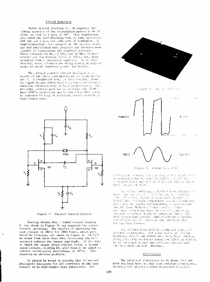
!;vbrid Modulator
Earth s t a t i o n t r a c k i n g of '. IK r e q u i r e s thet iming accuracv of the t r a n s m i t t e d p u l s e s to be a tl e a s t a s ^oud as 1 pa r t in 1 0 ' . Th is requi rer.entprec luded the s e l f - b l o c k i n g ?n>c^ of tube op i - ra t ion ,and i"ip» ried a neeu t o r some so r t ot modu la to r . Ah i g h - t e m p e r a t u r e t e s t pro^rart at M*l. se<. er.i i y e a r sago had e s t a b l i s h e d t h a t p rope r ly r u t c r y s t a l s werecapab1e of c a i n t a i n i n g the requ i red a c c u r a c y .Three c r v s t a l s (3 MH/., 5 '.'My., and 10 >iI1z, r e spec -t i v e l y ' cu t for min iuum dv i: t .u 125 C, iia\ e beenacqu i red from a t oiiir.erc i;» I sup:1'] i e r . .\> oi t h i swr i t i ng , the-s,1 i r t p s t a l s a r e bei::g t t -s ie;! a t ter.pi r -at urv to t v r i f v t u rnove r po Jnf •-• .nui dr i ' t >.
The t r y s a i l c o n t r o l c i r c u i t des i . ; :ud .is .iresuJ t of the above cons ider.i t ions i . '-l: ".;ii i n :' iv:-ure 7 . A bre.'itibo.i rd motie '. M l h i:- i' i r c n i i , i-hou*:!in F igure S, uas f a h r i r a i «.;1 i" r<*ri r:;Krr i,. I s r'?o;^i tvf unc l ion i-'at isi 'ac t or 11 y «;t i.i ^h t«-rpt.-i\it u r e s . Tl:e
dual JKET's o p e r a t i o n s and to d,-ter:"in, what •.•.-.>i: 1 dbe requi red to keep i t oper,»t i in; s.j* i - .;t t or ; :v ith igh tenper.iLur*. -
+V
v
-\a\
Ql Q2
I1,
Figure 7. Crystal '.'ontrol Circu i t
Testing showed that • timed ci rcui t I eedin»;<} (us shov.Ti in Figure 7) /as requ ired f-nr s i t i s-f ac tory .-»perat ion. Tlic resul t s of ope rat in;j, t hetest c i rcu i t at 280cC for J00+ hours* vhU'h pro-duced no f a i lu re s , are shown in Figure 9. It * i1jbe noted from these data that inc re.isinj* L he t en-pcrature reduces the output amplitude. If tlie r auat which the output drops remn ins f ixed, a sec<>ndtuned c i r c u i t , feeding Q2S will have t<> be added trachieve sat isfactory performance at 3J5 X. Thi prese-its no obvious problems.
It should be noted in passing that it was notabsolutely necessary for a l l c . i ter ials in the testc i r cu i t to be hiph-temperature substances. 1-ov
1.6V p
• •- :-•{><-;:<.::( U-u. -< MI-.~. p« r : r r . i J i I s f ',, . t r 'n. . ; : n:'.< -
t i ' - n , s H i M . : . - t o r i * . v .
•\-- •••: : h i s v r i t i / . i : . .., r*.*. L r . ^ 1 :*•-.!. ,• i i \ i; i i ':. -
• i < r i •-. i : : 1 : • : r i . J i ; . j : : . - . s j . ( • ; • • ; < ; • : - ; • . • < • ; « . • • . : i ; : • , - . •
'::•.•':: i" Id \:ui-. : - T h i ^ h v e - j u - r a t i - r i s t - j - . i ' / i ' c . p : u 3 u r l i - . i
: nV: U ) : r . ; 1 . * '.**•> 1 0 ) ••.c : -. : ' - l i n ; : I ' j . s i ' 1 - 1 . . ••,•!<.«*-
i: i ; h L V : " ; H r . i t u r e « p.-1-; Le-< . : n t i : ' i r : ; : i t i : J H - c i " ^ p o u n d s
I i i e f t ! ; i i e i i i t s t v i '. i b e t i ! i c ; i i ' t » -i u s i;:..', a i l
^ I s c r t - t e c . T . p . M H - n u s . l"i>r l a t e r t e : - i s i : n : : '. : -hi
h a r d w a r e , J N v . M a n t i 2%'SV^l u i < - > h - ' V f b e e : : . ' r d r f t i ,
a ] ' :n - w ^ t t : i h i p r e s i s t . ' r - r a l v d l . ^ r i ^ S *' -p r a i i c r
J t i s , ; ; i : i r i p a t d i h a t t h e O " ~ - : : . v t t v - i r ^ i ; . ' t v i i ;
f i t -Mn a r . i k i i > n a i 1 e r t i b . s t r a t e .
C o r y h a s L e n - ;
The princ : pal cone" Ens ic:; t^ be drav;i ;' ror. tiu-
vork reported here is ihat zumy ordinary c;>r:p.\-u :JIS
di*si ned for opt-rat ii\i under Ea. th.-norr:a I c« "*.: i-
120
C i o n s , tnay be u±>_'d i n ^:<z r e n t - e - i v i *"n:',:r.f n t >• ~ ~
c i t h e r " n t i i s , 1 " o r w i t h r n i n ^ r - ; . — : : : > ! i - r . i l e L-h.i:i>;-. •
i n t h e i r c o n s t r u c t i o n . A t S t . ; i . \ ; r>! s u - h <_•>•. i « : v . : -
a b i 1 i t i e r i w a n s t a r t ».*(! i>v p n . ' \ i--s.r; f t •:•..•,) n - h r r . ^ , ;:t<:
h a s W e n m n v ^ - m e i i b y t i n - f - r t - s v i i t w . - r k .
I n -idd i i i'.•:-), t ^r<.- .J 1 ;n- ; ] o j u - t - : u ] <•::! t : • ; ! -
; i b i ; i i v t!iJ*i"f:T:,ii i a n IN r t i : u - r . t t» '. p ; i r t i:nl . s r p r -
t - r .p I . i v ; :• .£ " t ' t ' U , ; l i . i : i . i il i r * v " t %-sl ; > i \ ' . • * • ; ; . ; r » ' ^ ,
o u s t t n - d e . ^ i ^-!>••:. ', •• l i t t i u : ! n . - i : s .>; • »t p r , i ; n : .
I n i - ! : r r a s e , ( V t n t h o u g h : : u c t - v . - 1 . ; O A > ? . « : V , U : i- i >
:i:»L vi,-1 b . . •.•:! t « - M r t i .):-, : c'•*"}•>] vl>- v M t ' % t : i *
p r . ' s j - i ' •!. t -. l i i r i ;n-- . i : : ' . • - • , ' . • . : : : ' ;:j- ;>!KJ_;» ; ( ;; i <•::. - r
t-Ju- M . i v - . ' i ^ t t ir.f-ii i?M.- «it. v r ' •-•;•. -v r . i - ^ ' • • - :< ~ ; . - • i .
H . - i i ^ j i - . i v i t y . rt--».*t.3 . w S t c h L - s , e t c . ) , - u i p e a v q u i l t -
b r i g h t . A t i h - i l t i r t - » - > u r p r i m - i p a l f . r i ' h i c r . wf 11
h c c i ' ^ c r . i ' t ' t i : i g i : t c 2 - k i ; r . j s . s ] i r i t . C.i v t - : : t h e
rv : - . ! : : t-7 c i1 J - i t e , i t : p ; u . I T S r i i : i t t h e v ^ n l y . s t ' t t i . i n
r i * q i . i r 3 ;:,-• . >:;«.;; .- i v t - r * < j t . - s : g r , h e r o v i 11 b e t l . c
pvr:""»rr.i*d atnia Institute
T . a m t : . : ^
121
IlKRHKn
by
Henry Walker, Director of Research, Permaluster, Inc., vurbaok, California
Ttie search by the electronic industry for componentsthat are light weight. More coapact, are capable of operat-ing in very high temperature and all environmental condi-tions is now proving rewarding.
The properties of such a flexible, transparent, thinfilm of aluminum oxide insulated wire or strip (with amelting point of 203O°C.) is unique for applications in theelectronic, missile, atoaic reactor, aerospace, and aircraftindustries. The oxide film is highly flexible, suitable fora l l windings of any s ize and shape of coi l (magnetic).Briefly touched upon are the ultraviolet, proton gamma ra-diation uses, as well as high vacuum and cryogenic applica-tions.
Since the film is inorganic and chemically inert, itdoes not age or deteriorate in storage and has gooddie lectr ic properties (1000 vol ts per n i l ) . In brief,components designed around this unique material wil l keepabreast of present day and future technology.
Designers of electro-magnetic components can nowachieve higher ratings per unit of weight and 3 reduction insine. With proper design, less insulation will be requiredand the dielectric losses are reduced.
The use of an aluminum conductor (round or rectangularwire or strips) will save 30% in weight, which is a distinctinprovement in commercial applications such as linearmotors, tbt-dical instruaents, etc., where lower mass willresult in lower inertia. Rotary equipment with low masssimplifies dynamic balancing. As vibration from dynamicimbalance is reduced, greater sensitivity and improved highfrequency response in aoving coil applications results fromthis lower mass. In al l , it is a dream cone true for mostengineers.
Compared to copper, aluminum with Al O-j insulationoperates cooler and will not oxidize. When operating temp-eratures of above 100° C, copper wi l l form an invisiblef i l a of cuprous oxide; above 200° C. cuprous and cuprieoxide are formed readily on the surface, thus reducing theconductance ac ultimately severe corrosion occurs and even-tually the conductor i s rendered useless. Even nickelcoated copper is subject to a galvanic action of the two•etals . In a high temperature operation, migration of atomsis created.
Performance of electrical components in high tempera-ture is seriously handicapped due to the lack of suitableinsulating aater ia l s as the components are subjected tosevere physical stresses in environmental conditions. Whenfailure occurs in organic insulation, the failure remainspermanent owing to the electrically conductive carbon paths
that are formed throughout the insulation as well as otherendangering problems, such as lack of adhesion, oxidation,evaporation, and aging.
Aging is accompanied by weight loss in organic materialwhere shrinkage results in the resin portion causing it tolose i t s bond in the s lot c e l l s , thus creating fai lure.Variation of temperature or rotating speed causes mechanicalabuses of the insulatiun. Thermal degeneration is fasterclose to the current-carrying conductors where the tempera-ture is at a maximum; Therefore, the failure is induced atthe hottest spot of the winding.
Aluminum conductor and AI9O3 insulation, which is cer-amic in nature, is free of galvanic action or oxidation. Incase of a breakdown, the insulation does not create trackingof a permanent conductive path throughout the insulation.In fact, oxide from the air creates a new insulated oxideand could repair itself. Therefore, it i s a good reason toconsider the relation between operating temperature andinsulation l i f e . A component made with high terapertureinsulated material wil l be more reliable and will protectitself and its payload from instant heat and pressure.
For several decades aluminum has been successfully em-ployed in the electrical engineering field and in variousother applications such as in transformers, generators,etc. , using bulky interleaving naterials such as paper,plastics, or laquer as insulation—far from satisfactory.
TAM.E I—Thermal and electrical conductin.tKS ofaluminum and capper.
Aluminum for electric conductors has a resistance ofabout 34.5 ohms/mm , which is equal to approximately 622 ofthe conductivity of e l ec t ro ly t i c copper. The spec i f icweight is 2.7 gm/ca , or about 30Z of that of copper. Thismeans that an aluminum conductor of equal conductivityweighs only 502 of that of a comparable copper conductor.In many cases, depending upon design, the conductive weightcan be further reduced depending on the dielectric loss, asaluminum operates cooler, and dissipates heat more rapidly.
Copper clad aluminum wire is re-inforced with EC gradealuminum conductor of an improved design developed to giveelectric power new versatility in construction. In additionto the contribution of i ts high strength to the conductor,i t adds to the total conductivity of the conductor, so thati t performs a dual function of strength and conductance. Of
123
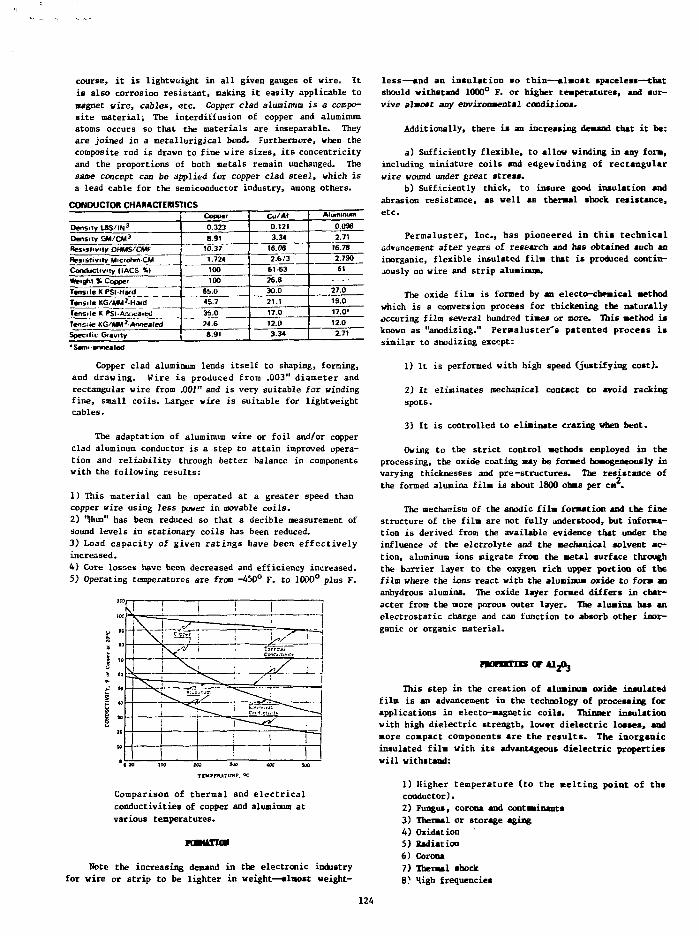
course, i t is lightweight in al l given gauges of wire. I tis also corrosion resistant, making i t easily applicable tomagnet wire, cables, etc. Copper clad aluminun i s a compo-si te material; The interdiffusion of copper and aluminumatoms occurs so that the materials are inseparable. Theyare joined in a metallurgical bond. Furthermore, when thecomposite rod is drawn to fine vire sizes, i t s concentricityand the proportions of both metals remain unchanged. Thecame concept can be applied for copper clad steel, which isa lead cable for the semiconductor industry, among others.
CONDUCTOR CHARACTERISTICS
Density IBS/IN3
Density GM/CM3
Resistivity OHMS/CMf
Resistivity Microhm CM
Conductivity (IACS %)
Weight % Copper
Tensile KPSIHjrd
Tensile KG/MM'-Hwd
Tensile K PSI-Ann«;alwJ
Tensile KG/MM '-Annealed
Specific G«avity
Copper
0.323
8.91
10.37
1.724
100
100
65.0
45.7
35.0
24.6
8.9.
Cu/AI
0.121
3.34
16.06
2.bl361-63
26.6
30.0
21.1
17.0
12.0
3.34
0.098
2.71
16.78
2.790
61
27.0
19.0
17.0-
12.0
2.71
°Semi-ennealed
Copper clad aluminum lends itself to shaping, forming,and drawing. Wire is produced from .003" diameter andrectangular wire from ,001" and is very suitable for windingfine, small coils. Larger wire is suitable for lightweightcables.
The adaptation of aluminum wire or foil and/or copperclad aluminum conductor is a step to attain improved opera-tion and reliability through better balance in componentswith the following results:
1) This material can be operated at a greater speed thancopper wire using less power in movable coils.2) 'Hum" has been reduced so that a decible measurement ofsound levels in stationary coils has been reduced.3) Load capacity of given ratings have been effectivelyincreased.4) Core losses have been decreased and efficiency increased.5) Operating temperatures are from -450° F. to 1000° plus F.
Comparison of thermal and e l ec t r i ca lconductivities of copper and aluminum atvarious temperatures.
FOMtnCM
Note the increasing demand in the electronic industryfor wire or strip to be lighter in weight—almost weight-
less—and an insulation so thin—almost spaceless—thatshould withstand 1000° F. or higher temperatures, and sur-vive almost any environmental conditions.
Additionally, there is an increasing demand that it be:
a) Sufficiently flexible, to allow winding in any form,including miniature coils and edgewinding of rectangularwire wound under great stress.
b) Sufficiently thick, to insure good insulation andabrasion resistance, as well as thermal shock resistance,etc.
Permaluster, Inc., has pioneered in this technicaladvancement after years of research and has obtained such aninorganic, flexible insulated film that is produced contin-uously on wire and strip aluminum.
The oxide film is formed by an electo-chemical methodwhich is a conversion process for thickening the naturallysecuring film several hundred times or more. This method isknown as "anodizing." Permaluster's patented process issimilar to anodizing except:
1) It is performed with high speed (justifying cost).
2) It eliminates mechanical contact to avoid rackingspots.
3) It is controlled to eliminate crazing when bent.
Owing to the strict control methods employed in theprocessing, the oxide coating may be formed homogeneously invarying thicknesses and pre -structures. The resistance ofthe formed alumina film is about 1800 ohms per en .
The mechanism of the anodic film formation and the finestructure of the film are not fully understood, but informa-tion is derived from the available evidence that under theinfluence of the elctrolyte and the mechanical solvent ac-tion, aluminum ions migrate from the metal surface throughthe barrier layer to the oxygen rich upper portion of thefilm where the ions react with the aluninum oxide to form ananhydrous alumina. The oxide layer formed differs in char-acter from the more porous outer layer. The alumina has anelectrostatic charge and can function to absorb other inor-ganic or organic material.
This step in the creation of aluminum oxide insulatedfilm is an advancement in the technology of processing forapplications in electo-magnetic coils. Thinner insulationwith high dielectric strength, lower dielectric losses, andmore compact components are the results. The inorganicinsulated film with its advantageous dielectric propertieswill withstand:
1) Higher temperature (to the melting point of theconductor).2) Fungus, corona and contaminants3) Thermal or storage aging4) Oxidation3) Radiation6) Corona7) Thermal shock8? High frequencies
124
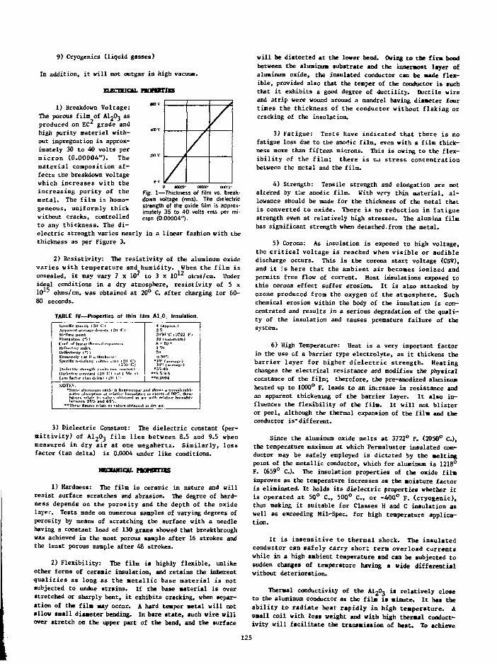
9) Cryogenics (liquid gasses)
In addition, it will not outgas in high vacuum.
ELECDUQU. ttanxms
1) Breakdown Voltage:The porous film of A12O3 asproduced on EC grade andhigh purity material with-out impregnation is approx-imately 30 to 40 volts permicron (0.00004"). Thematerial composition af-fects the breakdown voltagewhich increases with theincreasing purity of themetal. The film is homo-geneous, uniformly thickwithout cracks, controlledto any thickness. The di-electric strength varies nearly in a linear fashion with thethickness as per Figure 3.
2) Resistivity: The resistivity of the aluminum oxidevaries with temperature and humidity. When the film i sunsealed, i t may vary 7 x 10 to 3 x 10 oh-ns/cm. Underideal conditions in a dry atmosphere, resistivity of 5 x10 5 ohms/cm, was obtained at 20° C. after charging tor 60-80 seconds.
/
/
0 00OS~ 00050" 0U075-
Fig. 1—Thickness of film vs. break-down voltage (rms). The dielectricstrength of the oxide film is approx-imately 35 to 40 volts rms per mi-cron (0.00004").
TABLE IV—Properties
Specific K r \i\\ (20
Mt-Itint; pointKli>nv4lii>riCIH-1 nf InHcffjcti-t-
KmutivitySjHCific tc
Dii-l.-ttrivIJirlrrtrii-
NOTKS:•Sim,-» Mrthaurr
«Thr«
(1).4r l l , . ,,tldt-K
1 at f> v Ini intv .
" V " " " " "
of
•hms mil <
i IHKII-
> va1<n-
UU- to
C l
i i b\
•iht
valo
thin film Al 0
vrci
rax.'Jincii in a
-o »hla.ll(-<l
nsulation.
4 (appro*.)
2(1511 Cl(j | tnir8 x 1 0 *l 5a7(1
•1(1" fav
••0.WHM
nd thfiHt 4 ci
r with rehtit,
in dry air.
<3722'K)i mu m )
>itii)rrali1<-Hr-. Ihru-r humkltly
3) Dielectric Constant: The dielectric constant (per-mitt ivity) of A12O3 film l i e s between 8.5 and 9.5 whenmeasured in dry air at one megahertz. Similarly, lossfactor (tan delta) is 0.0004 under like conditions.
mauncu. nonmB
1) Hardness: The film is ceramic in nature and willresist surface scratches and abrasion. The degree of hard-ness depends on the porosity and the depth of the oxidelayer. Tests made on numerous samples of varying degrees ofporosity by means of scratching the surface with a needlehaving a constant load of 130 grams showed that breakthroughwas achieved in the most porous sample after 16 strokes andthe least porous sample after 48 strokes.
2) Flexibility: The film is highly flexible, unlikeother forms of ceramic insulation, and retains the inherentqualit ies as long as the metallic base material is notsubjected to undue strains. If the base material is overstretched or sharply bent, it exhibits cracking, when separ-ation of the film may occur. A hard temper metal will notallow mall diameter bending. In bare state, *uch wire willover stretch on the upper part of the bend, and the surface
will be distorted at the lower bend. Owing to the firm bondbetween the aluminum substrate and the innermott layer ofaluminum oxide, the insulated conductor can be made flex-ible, provided also that the temper of the conductor is suchthat it exhibits a good degree of ductility. Ductile wireand strip were wound around a mandrel having diameter fourtimes the thickness of the conductor without flaking orcracking of the insulation.
3) Fatigue: Tests have indicated that there is nofatigue loss due to the anodic film, even with a film thick-ness more than fifteen microns. This is owing to the flex-ib i l i ty of the film; there i s na stress concentrationbetween the metal and the film.
4) Strength: Tensile strength and elongation are notaltered by tiie anodic film. With very thin material, al-lowance should be made for the thickness of the metal thatis converted to oxide. There i s no reduction in fatiguestrength even at relatively high stresses. The alumina filmhas significant strength when detached. from the metal.
5) Corona: As insulation is exposed to high voltage,the cr i t i ca l voltage is reached when v i s ib le or audibledischarge occurs. This is the corona start voltage (CSV),and i t i s here that the ambient air becomes ionized andpermits free flow of current. Host insulations exposed tothis corona effect suffer erosion. It is also attacked byozone produced from the oxygen of the atmosphere. Suchchemical erosion within the body of the insulation is con-centrated and results in a serious degradation of the quali-ty of the insulation and causes premature failure of thesystem.
6) High Temperature: Heat is a very important factorin the use of a barrier type electrolyte, as i t thickens thebarrier layer for higher die lectr ic strength. Heatingchanges the electrical resistance and modifies the physicalConstance of the film; therefore, the pre-anodized aluminumheated up to 1000° F. leads to an increase in resistance andan apparent thickening of the barrier layer. It also in-fluences the flexibility of the film. It will not blisteror peel, although the thermal expansion of the film and theconductor is* different.
Since the aluminum oxide melts at 3722° F. (2050° C),the temperature maximum at which Permaluster insulated con-ductor may be safely employed is dictated by the aeltingpoint of the metallic conductor, which for aluminum is 1218°F. (659° C). The insulation properties of the oxide filmimproves as the temperature increases as the moisture factoris eliminated. It holds i t s dielectric properties whether i ti s operated at 50° C, 500° C, or -400° F. (cryogenic),thus making i t suitable for Classes H and C insulation aswell as exceeding Mil-Spec, for high temperature applica-tion.
It i s insensitive to thermal shock. The insulatedconductor can safely carry short term overload currentswhile in a high ambient temperature and can be subjected tosudden changes of temperature having a wide differentialwithout deterioration.
Thermal conductivity of the A12O3 is relatively clo»eto the aluminum conductor as the film is minute. It has theabi l i ty to radiate heat rapidly in high temperature. Asnail coil with lets weight and with high thermal conduct-ivity will facilitate the tran»iiaion of heat. To achieve
125
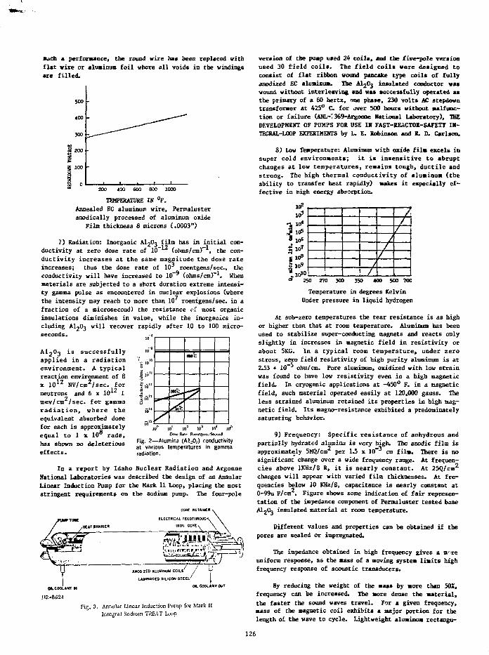
such a performance, the round wire his been replaced withflat wire or aluminum foil where all voids in the windingsare filled.
" 200 400 600 800 1000
TEMPERATURE IN °F.Annealed EC aluminum wire, Permalusteranodically processed of aluminum oxide
Filn thickness 8 microns (.0003")
7) Radiation: Inorganic AI2O3 film has in initial con-ductivity at zero dose rate of 10" (ohms/cm) , the con-ductivity increases at the same magnitude the dose rateincreases; thus the dose rate of 10 roentgens/sec., theconductivity will have increased to 10"' (ohms/cm) . Whenmaterials are subjected to a short duration extreme intensi-ty gamma pulse as encountered in nuclear explosions (wherethe intensity may reach to more than 10 roentgens/sec. in afraction of a microsecond) the resistance o.C most organicinsulations diminishes in value, while the inorganics in-cluding AI2O3 will recover rapidly after 10 to 100 micro-seconds.
AI2O3 i s successfullyapplied in a radiationenvironment. A typicalreaction environment of 8x 101Z NV/cm2/sec. forneutrons and 6 x l<r 1mev/cm /sec. for gammaradia t ion , where theequivalent absorbed dosefor each is approximatelyequal to 1 x 10° rads,has shown no deleteriouseffects.
MOC,,
/Sob
m e
!'°J.6-
Jf."
10" 101 10* 10* itf* 10s
Doje Bale Roenrgera/Snond
Fig. 2—Alumina (Al20: i) conductivityat various temperatures in gammaradiation.
In a report by Idaho Nuclear Radiation and ArgonneNational Laboratories was described the design of an AnnularLinear Induction Pump for the Mark 11 Loop, placing the moststringent requirements on the sodium pump. The four-pole
oc cooi.*NT our
y
//
Fig. 3. Annular Linear Induction Pump for Mark IIIntegra! Sodium TREAT Loop
version of the pump used 24 co i l s , and the five-pole versionused 30 H e l d c o i l s . The f i e l d c o i l s were designed toconsist of f lat ribbon wound pancake type coi ls of fullyanodized EC aluminum. The AI2O3 insulated conductor va*wound without interleaving and was successfully operated asthe primary of a 60 hertz, one phase, 230 volts AC stepdowntransformer at 425° C. for over 500 hours without malfunc-tion or failure (AHL-7369-Argonne National Laboratory), THEDEVELOPHEHT OF PUMPS FOR USE IH FAST-REACTOR-SAFETY IH-TEGRAL-LOOP EXPERIMENTS by L. E. Robinson and R. D. Carlson.
3) Low Temperature: Aluminum with oxide film excels insuper cold environments; i t i s in sens i t i ve to abruptchanges at low temperatures, remains tough, duct i l e andstrong. The high thermal conductivity of aluminum (theability to transfer heat rapidly) makes i t especially ef-fective in high energy absorption.
V?
>10«
<* 2 5 0 2 7 0 3 0 0 350 400 500 70C
Temperature in degrees KelvinUnder pressure in liquid hydrogen
At sub-zero temperatures the tear resistance is as highor higher than that at room temperature. Aluminum has beenused to stabilize super-conducting magnets and reacts onlyslightly in increases in magnetic field in resistivity orabout 5KG. In a typical room temperature, under zerostress, zero field resistivity of high purity aluminum is at2.53 + 10 ohm/cm. Pure aluminum, oxidized with low strainwas found to have low resistivity even in a high magneticfield. In cryogenic applications at -450° F. in a magneticfield, such material operated easily at 120,000 gauss. Theless strained aluminum retained i ts properties in high mag-netic field. Its magno-resistance exhibited a predominatelysaturating behavior.
9) Frequency: Specific resistance of anhydrous andpartially hydratcd alumina is very high. The anodic film isapproximately 5MQ/cm per 1.5 x 10 cm film. There is nosignificant change over a wide frequency range. At frequen-cies above lKHz/S R, i t i s nearly constant. At 25Q/cnchanges will appear with varied film thicknesses. At fre-quencies below 10 KHz/S, capacitance is nearly constant at0-99u F/cm . Figure shows some indication of fair represen-tation of the impedance component of Pernaluster tested baseAI2O0 insulated material at room temperature.
Different values and properties can be obtained if thepores are sealed or impregnated.
The impedance obtained in high frequency gives a mr.reuniform response, as the mass of a moving system limits highfrequency response of acoustic transducers.
By reducing the weight of the mass by more than 502,frequency can be increased. The more dense the material,the faster the sound waves travel. For a given frequency,mass cf the magnetic coil exhibits a major portion for thelength of the wave to cycle. Lightweight aluminum rectangu-
126
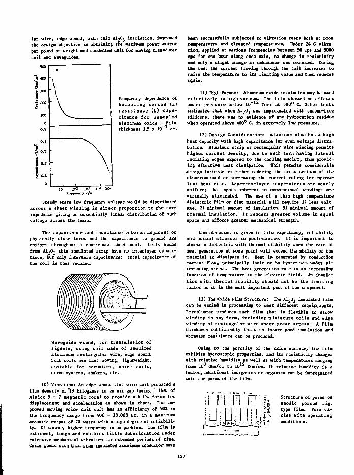
lar wire, edge wound, with thin AljOj insulation, improvedthe design objective in obtaining the maximum power outputper pound of weight and condensed unit for moving transducercoil and waveguides.
Frequency dependence ofbalancing series Ca)resistance (b) capa-citance for annealedaluminum oxide - Filmthickness l.S x 10 cm.
10 10? 103 10*Frequency c/o
Steady state low frequency voltage would be distributedacross a sheet winding in direct proportion to the turnimpedance giving an essentially linear distribution of suchvoltage across the turns.
The capacitance and inductance between adjacent orphysically close turns and the capacitance to ground areuniform throughout a continuous sheet coil. Coils woundfrom A^Oj thin insulated strip have no interlayer capaci-tance, but only interturn capacitance; total capacitance ofthe coil is thus reduced.
Waveguide wound, for transmission ofsignals, using coil made of anodizedaluminum rectangular wire, edge wound.Such coils are fast moving, lightweight,suitable for actuators, voice coils,servo systems, shakers, etc.
10) Vibration: An edge wound flat wire coil produced aflux density of *18 kilogauss in an air gap (using 3 lbs. ofAlnico 5 - 7 magnetic core) to provide a 6 lb. force fordisplacement and acceleration as shown in chart. The im-proved moving voice coil nnit has an efficiency of 50% inthe frequency range from 400 - 10,000 Hz. in a maximumacoustic output of 20 watts with a high degree of reliabili-ty. Of course, higher frequency is no problem. The film isextremely tough and exhibits little deterioration underextensive mechanical vibration for extended periods of tiae.Coils wound with thin film insulated aluminum conductor have
been successfully subjected to vibration tests both at roomtemperatures and elevated temperatures. Under 24 G vibra-tion, applied at various frequencies between 50 cps and 5000cps for one hour along each axis, no change in resistivityand only a slight change in inductance was recorded. Duringthe test the current flowing through the coil increases toraise the temperature to its limiting value and then reducessgain.
11) High Vacuum: Aluminum oxide insulation may be usedeffectively in high vacuun. The film showed no effectsunder pressure below 10 Torr at 500° C. Other testsindicated that when A^Oj was impregnated with carbon-freesilicons, there was no evidence of any hydrocarbon residuewhen operated above 400° C. in extremely low pressure.
12) Design Consideration: Aluminum also has a highheat capacity with high capacitance for even voltage distri-bution. Aluminum strip or rectangular wire winding permitshigher current density, due to each turn having lateralradiating edges exposed to the cooling medium, thus provid-ing effective heat dissipation. This permits considerable-design latitude in either reducing the cross section of thealuminum used or increasing the current rating for equiva-lent heat rise. Layer—to—layer temperatures are nearlyuniform; hot spots inherent in conventional windings arevirtually eliminated. The use of a thin high temperaturedielectric film on flat material will require 1) less volt-age, 2) minimal amount of insulation, 3) minimal amount ofthermal insulation. It renders greater volume in equalspace and affords greater mechanical strength.
Consideration is given to life expectancy, reliabilityand normal stresses in performance. It is important tochoose a dielectric with thermal stability when the rate ofheat generation at some point will exceed the ability of thematerial to dissipate it. Heat is generated by conductioncurrent flow, principally ionic or by hysteresis under al-ternating stress. The heat generation rate is an increasingfunction of temperature in the electric field. An insula-tion with thermal stability should not be the limitingfactor as it is the most important part of the component.
13) The Oxide Film Structure: The A^Oj insulated filmcan be varied in processing to meet different requirements.Permaluster produces such film that is flexible to allowwinding in any form, including miniature coils and edgewinding of rectangular wire under great stress. A filmthickness sufficiently thick to insure good insulation andabrasion resistance can be produced.
Owing to the porosity of the oxide surface, the filmexhibits hydroscopic properties, and its resistivity changeswith relative humidity as well as with temperatures rangingfrom 108 Ohm/cm to 1012 Ohm/cm. If relative humidity is afactor, additional inorganics or organics can be impregnatedinto the pores of the film.
*WV'Ti
lyyi-JiiJiStructure of pores onanodic porous fig.type film. Pore va-ries with operatingconditions•
127
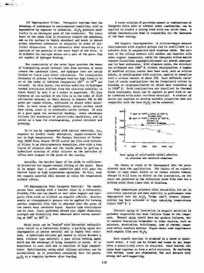
14) Impregnated Films: Inorganic coatings have theadvantage of resistance to environmental'conditions, with nodegradation by exposure to radiation. AI7O? produced anod-ically is an intergral part of the conductor. The innerlayer of the oxide film is relatively compact and anhydrous,and on the surface is highly absorbent and ready to absorbeither dissolved substances or molecules in state of col-loidal dispersion. It is axiomatic that absorbing is afunction of the porosity of the outer layer of the film. Itis probable the oxy-type anions are a part of the pores thatare capable of hydrogen bonding.
The conductivity of the outer layer provides the meansof transporting anions hydroxyl ions from solvents or watertoward the condensed layer, and hydrogen ions are easilybonded or fused with other substances. The transistionfrequency of protons in a hydrogen bond has been found to beon of the order of infrared frequencies (10 to 10 1 4 persecond). On this basis, the proton mobility in hydrogenbonded structures differs from the electron mobility inmetal itself by only 1 or 2 orders in magnitude. The porediameter of the surface of the film is in the order of 10.50millimeter microns, or their density is between 100 to 800pores per square micron, sufficient to absorb other mater-ials. In soire areas of applications, porous surface couldhave value, since it is chemically active surface. It actsas a good agent for mechanical bonding; other advantagesinclude its retention of photo-litho emulsions, and itserves as a base for electroplating, printed circuitry andpainting.
Pores can be impregnated with various materials, i.e.,organics to inhibit water absorption, organo-ceramics foruse in high temperatures. The Georgia Institute of Techno-logy (WADC Tech. Report 58-13) sealed the film with Colloid-al Silica in an electrophoresis deposition, also with a trueliquid of ceramics that wet the inside pores by gelling ahydrolized solution of ethyl silicate so the particles ofsilica were trapped in the pores of the coating.
Actually, the barrier layer of the oxide is sufficient-ly protective for organo-ceramic filling of the pores. Thereis no danger that a carbon conductive path will pass thebarrier layer in high temperature operation. In fact, eventhe organic material will operate at twice the temperaturewithout effect.
15) Impregnation With Inorganic Material: The anodicporous base coating with a barrier layer is a refractory,flexible film and can absorb or seal other organic and inor-ganic film with or without an organic vehicle. Anotheranodic or eletropboretic process can be applied for forminganother composite film that is absorbed into the pores ofthe anodic base insulated layer. Barrier type electrolytescan be used. Tests performed showed that higher dielectricstrength and flexibility were obtained after vacuum anneal-ing at 450° to 500° C.
Oxide pores can be "sealed" with Tetraethyl orthosili-cate, which is a refractory binder, a gelling agent forimpregnation of porous material and is highly heat resis-tant. A hydrolized silicate gel heated to silica becomes ahard, vitreous type material; a pure silica bonding agentwhich has the advantage of being insoluble in water. It isimpervious to most acid and is excellent in high tempera-tures. Hydrolization, using ethyl silicate solution, can beaccomplished, as it penetrates completely into the porousXi2°3 to a complete hardness after heating.
A water solution of porcelain enamel or combination* ofinorganic fritz with or without resin combination, can beapplied to create a strong bond with the oxide baie. Astrong intermolecular bond is responsible for the inertnessof the base coating.
16) Organic Impregnation: A silicon-oxygen networkinterspersed with organic groups can be stabilized to avaluable film in conjunction with aluminum oxide. The sol-vent of the silicon mixture will oxidize and vaporize withother organic components, while the inorganic silica matrixremains (crosslined organopolysiloxans) are almost unsurpas-sed Cor heat resistance. With aluminum oxide, the structurecan withstand over 1400° F. without deterioration. A numberof modified silicon resins have been used, such as siliconalkyds, or modifications with acrylics, epoxies or phenolicswith a silicon content of about 252. Such different varie-ties of resin combinations can be formulated either byblending or co-polymerization to obtain heat resistance upto 1000° F. Such combinations are excellent in thermalshock resistance. Resin can be applied in pure form or canbe combined with other resinous material. A mixture ofresins put together to develop suitable properties that arecompatible with the base A^O? can be achieved.
_ 1000
0 A«ed at 500°F.,tested at 500° T.lp y m r only
tt> Aged et 700°?., tested at 700° T.polymer onanodlsed
d ° 1000 2000 3000 4000 hr»
1Heat aging of poly-(amide-imide) adhesive
on aluminun and anodized aluainuo.
The choice of resin to be impregnated into the poresdepends upon the application. The choice of an organicbinder is made where l i t t le or no carbon residue remain,though i t wi l l have no effect on the insulation, as thepores are protected by the refractory oxide film that has amelting point three times that of aluminum.
High temperature polymers offer versatility for use inelectronic insulation and show stability in performance whenimpregnated into the AI2O3 "prime coat"; Greater depend-ability has been achieved at high operating temperatures(about 850° F. ).
Thermal aging of insulation in organic material i sprobably responsible for most failures found in the compo-nent. Thermal aging itself does not produce failures, butit renders insulation vulnerable to other factors, such asmoisture, penetration, brittleness, loss of thermal expan-sion before complete failure. Figure shows some experimentswith organic film over Mfly
Such organic overcoat is produced in a cured or quasi-cured state. A coil can be formed and wound in any shapewhen a quasi-cured state i s required. When heated, theturns bond together to form a solid structure. By employingthis method, cores are eliminated; The coil becoues verystrong and self-supporting.
128
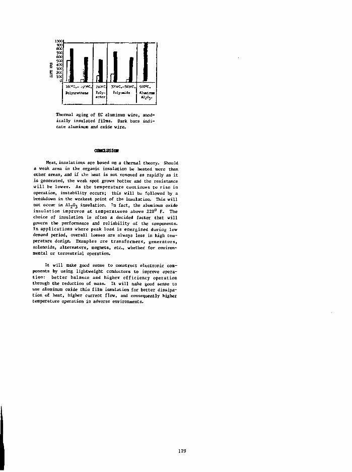
1000900
7006005O0
| 400
3 1000 ll
1K*C- i«0C.Polyunttene
J240OC,
P o l y -
ester
\l3?»C.-360OC.
Folyuude
1500°C.
JUusdma11203.
Thermal aging of EC aluminum wire, anod-ica l ly insulated f i lms. Dark bars indi-cate aluminum and oxide wire.
OOKLOSIM
Most, insulations are based on a thermal theory. Shoulda weak area in the organic insulation be heated more thanother areas, and if the lieat is not removed as rapidly as itis generated, the weak spot grows hotter and the resistancewill be lower. As the temperature continues to rise inoperation, instability occurs; this will be followed by abreakdown in the weakest point of th» insulation. This willnot occur in AI2O3 insulation. Tn fact, the aluminum oxideinsulation improves at temperatures above 220° F. Thechoice of insulation is often a decided factor that willgovern the performance and reliability of the components.In applications where peak load is energized during lowdemand period, overall losses are always less in high tem-perature design. Examples are transformers, generators,solenoids, alternators, magnets, etc., whether for environ-mental or terrestrial operation.
It will make good sense to construct electronic com-ponents by using lightweight conductors to improve opera-tion: better balance and higher efficiency operationthrough the reduction of mass. It will make good sense touse aluminum oxide thin film insulation for better dissipa-tion of heat, higher current flow, and consequently highertemperature operation in adverse environments.
129
S E S S I O N V I
S P E C I A L K E Y N O T E A D D R E S S
A C O N F E R E N C E P E R S P E C T I V E
Technology Transfer and Commercialization of High Temperature Electronics
Dr. Robert PryGould, Inc.Boiling Meadows, Illinois
Dr. Robert Pry, Executive Vice President for R and D, Gould, Inc., has beeninvited to the conference to listen to the proceedings, have discussions with theauthors and attendees and from this background provide insights on the status ofeffort, interfaces between, and perception of the research, manufacturing anduser communities in high temperature electronics. The progress of R and D, fabrica-tion technology and commercialization of useful measurement systems at temperaturesgreater than 200°C «ill be assessed. The gaps between user needs, R and D resultsand on-going projects will be summarized yielding market expectations as projectedfrom user applications and manufacturer viewpoints. The apparent determinants forcommeT .-ialization of current research projects and the perceived interface barriersto technology transfer will be detailed.
Related Documents


