Fig. 1. Boost converter with auxiliary step-up circuit. Fig. 2. Proposed boost converter integrated with voltage-doubler. Fig. 3. Key waveforms in BR region. High Step-up Boost Converter Integrated with Voltage-Doubler Ki-Bum Park, Gun-Woo Moon, and Myung-Joong Youn Department of Electrical Engineering, KAIST, Daejeon, Republic of Korea E-mail: [email protected] Abstract -- The voltage-doubler provides an additional step- up gain on top of that of the boost converter, while distributing voltage stresses on devices as well. The interface between the boost converter and the voltage-doubler is accomplished by a transformer and a balancing capacitor, which also constitute a resonant tank. Since this resonant operation shapes the current sinusoidal, a switch turn-off loss and a reverse recovery on diode can be reduced. Therefore, the proposed converter is promising for high step-up applications with high efficiency Index Terms— Boost converter and voltage-doubler. I. INTRODUCTION For a battery powered system, electric vehicles, fuel cell system, and photovoltaic systems, where low voltage sources need to be converted to a high voltage of output, non-isolated high step-up conversion techniques find increasing necessities. A classical boost converter is generally used for its simple structure and continuous input current. However, it is hard to satisfy both high voltage conversion ratio and high efficiency at the same time with a plain boost converter. In high output voltage applications, moreover, high voltage stress on switch and diode degrades the performance of devices, causing a severe hard switching loss, a conduction loss, and a reverse recovery problem [1]-[8]. To relieve abovementioned limitations in high step-up applications, various types of step-up techniques can be applied [4]-[14]. A coupled-inductor boost converter is a favorable candidate for its simple structure, however an input current ripple is large and an auxiliary circuit is required to suppress the switch voltage spike [5]-[9]. A voltage multiplier cell or a switch-capacitor circuit can be useful to raise a step- up gain in collaboration with classical topologies [10]-[12]. As the output voltage is increased, however, the number of stage is increased, requiring more capacitors and diodes. Besides, a current snubber is required to reduce the reverse recovery on diode. To raise step-up gain of a boost converter further in non- isolated applications, the alternative structure, which combines a boost converter with an auxiliary circuit in series, can be considered as shown in Fig. 1 [15],[16]. Proper selection of an auxiliary module can give many advantages such as high step-up capability, design flexibility, and distributed voltage stress. In this paper, as an auxiliary step- up circuit, the voltage-doubler is integrated with a boost converter as shown in Fig. 2 [17]. The voltage stresses on the diodes D o2 and D o3 in the volage-doubler are clamped to its 978-1-4244-5287-3/10/$26.00 ©2010 IEEE 810

Welcome message from author
This document is posted to help you gain knowledge. Please leave a comment to let me know what you think about it! Share it to your friends and learn new things together.
Transcript
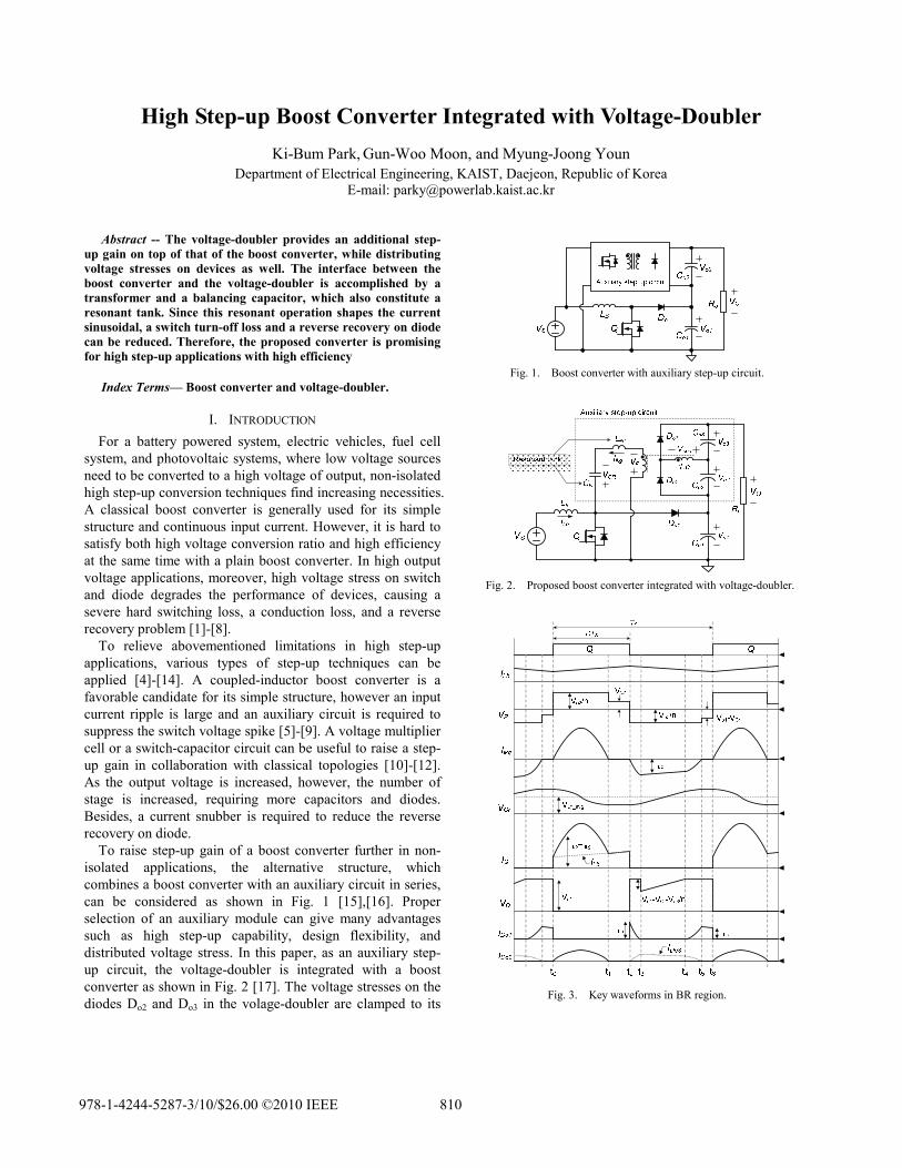
Fig. 1. Boost converter with auxiliary step-up circuit.
Fig. 2. Proposed boost converter integrated with voltage-doubler.
Fig. 3. Key waveforms in BR region.
High Step-up Boost Converter Integrated with Voltage-Doubler
Ki-Bum Park, Gun-Woo Moon, and Myung-Joong Youn Department of Electrical Engineering, KAIST, Daejeon, Republic of Korea
E-mail: [email protected]
Abstract -- The voltage-doubler provides an additional step-up gain on top of that of the boost converter, while distributing voltage stresses on devices as well. The interface between the boost converter and the voltage-doubler is accomplished by a transformer and a balancing capacitor, which also constitute a resonant tank. Since this resonant operation shapes the current sinusoidal, a switch turn-off loss and a reverse recovery on diode can be reduced. Therefore, the proposed converter is promising for high step-up applications with high efficiency
Index Terms— Boost converter and voltage-doubler.
I. INTRODUCTION For a battery powered system, electric vehicles, fuel cell
system, and photovoltaic systems, where low voltage sources need to be converted to a high voltage of output, non-isolated high step-up conversion techniques find increasing necessities. A classical boost converter is generally used for its simple structure and continuous input current. However, it is hard to satisfy both high voltage conversion ratio and high efficiency at the same time with a plain boost converter. In high output voltage applications, moreover, high voltage stress on switch and diode degrades the performance of devices, causing a severe hard switching loss, a conduction loss, and a reverse recovery problem [1]-[8].
To relieve abovementioned limitations in high step-up applications, various types of step-up techniques can be applied [4]-[14]. A coupled-inductor boost converter is a favorable candidate for its simple structure, however an input current ripple is large and an auxiliary circuit is required to suppress the switch voltage spike [5]-[9]. A voltage multiplier cell or a switch-capacitor circuit can be useful to raise a step-up gain in collaboration with classical topologies [10]-[12]. As the output voltage is increased, however, the number of stage is increased, requiring more capacitors and diodes. Besides, a current snubber is required to reduce the reverse recovery on diode.
To raise step-up gain of a boost converter further in non-isolated applications, the alternative structure, which combines a boost converter with an auxiliary circuit in series, can be considered as shown in Fig. 1 [15],[16]. Proper selection of an auxiliary module can give many advantages such as high step-up capability, design flexibility, and distributed voltage stress. In this paper, as an auxiliary step-up circuit, the voltage-doubler is integrated with a boost converter as shown in Fig. 2 [17]. The voltage stresses on the diodes Do2 and Do3 in the volage-doubler are clamped to its
978-1-4244-5287-3/10/$26.00 ©2010 IEEE 810
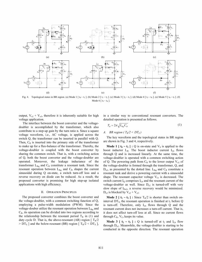
(a) (b) (c)
(d) (e) (f)
Fig. 4. Topological states in BR region. (a) Mode 1 [ t0 ~ t1 ]. (b) Mode 2 [ t1 ~ t2 ]. (c) Mode 3 [ t2 ~ t3 ]. (d) Mode 4 [ t3 ~ t4 ]. (e) Mode 5 [ t4 ~ t5 ]. (f) Mode 6 [ t5 ~ t6 ].
output, Vo2 + Vo3, therefore it is inherently suitable for high voltage application.
The interface between the boost converter and the voltage-doubler is accomplished by the transformer, which also contribute to a step-up gain by the turn ratio n. Since a square voltage waveform, i.e., AC voltage, is applied across the switch Q, the transformer can be inserted in parallel with Q. Then, CR is inserted into the primary side of the transformer to make up for a flux-balance of the transformer. Thereby, the voltage-doubler is coupled with the boost converter by sharing the common switch. That is, with a switching action of Q, both the boost converter and the voltage-doubler are operated. Moreover, the leakage inductance of the transformer Llkg and CR constitute a resonant tank. Since the resonant operation between Llkg and CR shapes the current sinusoidal during Q on-state, a switch turn-off loss and a reverse recovery on diode can be reduced. As a result, the proposed converter is promising for high step-up isolated applications with high efficiency.
II. OPERATION PRINCIPLES The proposed converter combines the boost converter and
the voltage-doubler, with a common switching function of Q, employing a pulse-width modulation (PWM). Since the voltage-douber utilize the resonant operation between Llkg and CR, its operation can be divided into two regions according to the relationship between the resonant period TR in (1) and duty cycle D. That is, the above-resonant (AR) region [ TR/2 > DTS ] and the below-resonant (BR) region [ TR/2 < DTS ],
in a similar way to conventional resonant converters. The detailed operation is presented as follows.
2R lkg RT L Cp= (1)
A. BR region ( TR/2 < DTS ) The key waveform and the topological states in BR region
are shown in Fig. 3 and 4, respectively. Mode 1 [ t0 ~ t1 ] : Q is on-state and VS is applied to the
boost inductor LB. The boost inductor current ILb flows through Q and is increased linearly. At the same time, the voltage-doubler is operated with a common switching action of Q. The powering path from CR to the lower output Vo2 of the voltage-doubler is formed through the transformer, Q, and Do2, as presented by the dotted line. Llkg and CR constitute a resonant tank and derive a powering current with a sinusoidal shape. The resonant capacitor voltage VCr is decreased. The switch current IQ comprises ILb and the resonant current of the voltage-doubler as well. Since Do2 is turned-off with very slow slope of IDo2, a reverse recovery would be minimized. Do3 is blocked by Vo2 + Vo3.
Mode 2 [ t1 ~ t2 ] : Since TR/2 is shorter than switch on-interval DTS, the resonant operation is finished at t1 before Q is turn-off. Therefore, only ILb flows through Q and the resonant current does not increases a turn-off current. That is, it does not affect turn-off loss at all. Since no current flows through CR, VCr keeps its value.
Mode 3 [ t2 ~ t3 ] : Q is turned-off at t2 and ILb flow through Do1. Meanwhile, the voltage-doubler is starting to be conducted in the opposite direction. The resonant operation
811
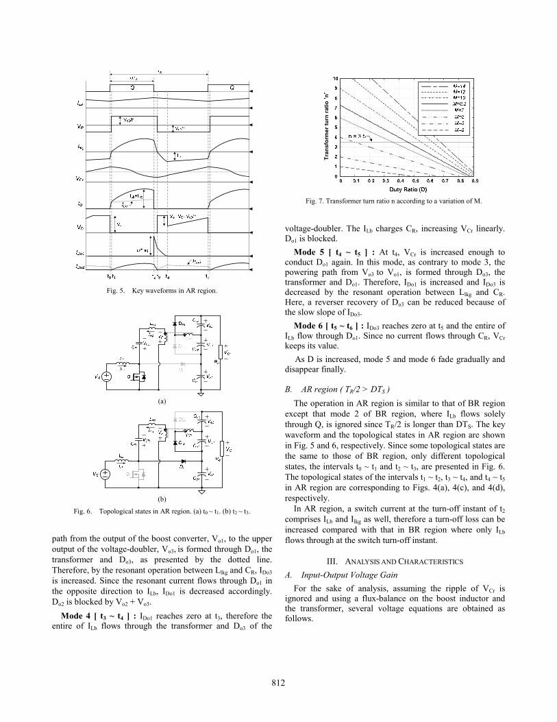
Fig. 5. Key waveforms in AR region.
(a)
(b)
Fig. 6. Topological states in AR region. (a) t0 ~ t1. (b) t2 ~ t3.
Tran
sfor
mer
turn
ratio
n
Fig. 7. Transformer turn ratio n according to a variation of M.
path from the output of the boost converter, Vo1, to the upper output of the voltage-doubler, Vo3, is formed through Do1, the transformer and Do3, as presented by the dotted line. Therefore, by the resonant operation between Llkg and CR, IDo3 is increased. Since the resonant current flows through Do1 in the opposite direction to ILb, IDo1 is decreased accordingly. Do2 is blocked by Vo2 + Vo3.
Mode 4 [ t3 ~ t4 ] : IDo1 reaches zero at t3, therefore the entire of ILb flows through the transformer and Do3 of the
voltage-doubler. The ILb charges CR, increasing VCr linearly. Do1 is blocked.
Mode 5 [ t4 ~ t5 ] : At t4, VCr is increased enough to conduct Do1 again. In this mode, as contrary to mode 3, the powering path from Vo3 to Vo1, is formed through Do3, the transformer and Do1. Therefore, IDo1 is increased and IDo3 is decreased by the resonant operation between Llkg and CR. Here, a reverser recovery of Do3 can be reduced because of the slow slope of IDo3.
Mode 6 [ t5 ~ t6 ] : IDo3 reaches zero at t5 and the entire of ILb flow through Do1. Since no current flows through CR, VCr keeps its value.
As D is increased, mode 5 and mode 6 fade gradually and disappear finally.
B. AR region ( TR/2 > DTS )
The operation in AR region is similar to that of BR region except that mode 2 of BR region, where ILb flows solely through Q, is ignored since TR/2 is longer than DTS. The key waveform and the topological states in AR region are shown in Fig. 5 and 6, respectively. Since some topological states are the same to those of BR region, only different topological states, the intervals t0 ~ t1 and t2 ~ t3, are presented in Fig. 6. The topological states of the intervals t1 ~ t2, t3 ~ t4, and t4 ~ t5 in AR region are corresponding to Figs. 4(a), 4(c), and 4(d), respectively.
In AR region, a switch current at the turn-off instant of t2 comprises ILb and Ilkg as well, therefore a turn-off loss can be increased compared with that in BR region where only ILb flows through at the switch turn-off instant.
III. ANALYSIS AND CHARACTERISTICS A. Input-Output Voltage Gain
For the sake of analysis, assuming the ripple of VCr is ignored and using a flux-balance on the boost inductor and the transformer, several voltage equations are obtained as follows.
812
(a)
Duty Ratio (D)0.1 0.2 0.3 0.4 0.5 0.6 0.7 0.8 0.9
0
2
4
6
8
10
12
14
16
18
20
Switc
h rm
s cu
rren
t nor
mal
ized
by
Io
M = 12
M = 10
M = 8.3
M = 7
M = 5
M = 3M = 2
n = 3.5
(b)
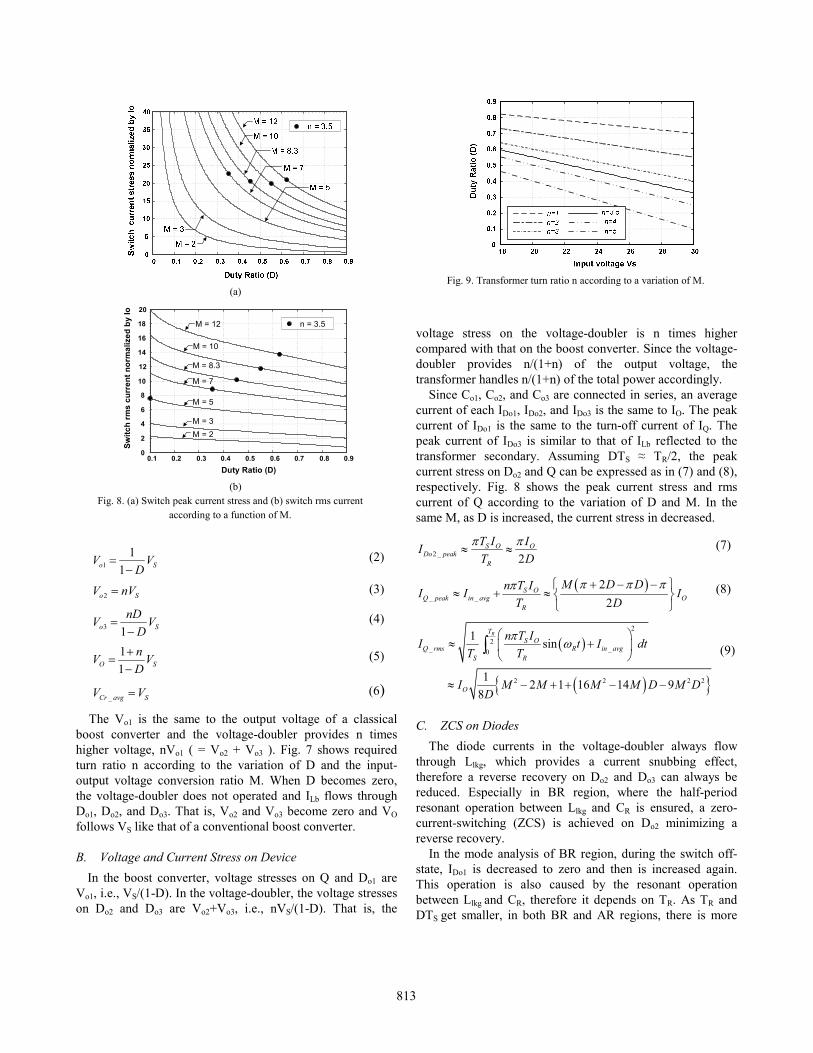
Fig. 8. (a) Switch peak current stress and (b) switch rms current according to a function of M.
Fig. 9. Transformer turn ratio n according to a variation of M.
11
1o SV VD
=-
(2)
2o SV nV= (3)
3 1o SnDV V
D=
- (4)
11O S
nV VD
+=
- (5)
_Cr avg SV V= (6)
The Vo1 is the same to the output voltage of a classical boost converter and the voltage-doubler provides n times higher voltage, nVo1 ( = Vo2 + Vo3 ). Fig. 7 shows required turn ratio n according to the variation of D and the input-output voltage conversion ratio M. When D becomes zero, the voltage-doubler does not operated and ILb flows through Do1, Do2, and Do3. That is, Vo2 and Vo3 become zero and VO follows VS like that of a conventional boost converter.
B. Voltage and Current Stress on Device
In the boost converter, voltage stresses on Q and Do1 are Vo1, i.e., VS/(1-D). In the voltage-doubler, the voltage stresses on Do2 and Do3 are Vo2+Vo3, i.e., nVS/(1-D). That is, the
voltage stress on the voltage-doubler is n times higher compared with that on the boost converter. Since the voltage-doubler provides n/(1+n) of the output voltage, the transformer handles n/(1+n) of the total power accordingly.
Since Co1, Co2, and Co3 are connected in series, an average current of each IDo1, IDo2, and IDo3 is the same to IO. The peak current of IDo1 is the same to the turn-off current of IQ. The peak current of IDo3 is similar to that of ILb reflected to the transformer secondary. Assuming DTS ≈ TR/2, the peak current stress on Do2 and Q can be expressed as in (7) and (8), respectively. Fig. 8 shows the peak current stress and rms current of Q according to the variation of D and M. In the same M, as D is increased, the current stress in decreased.
2 _ 2S O O
Do peakR
T I IIT D
p p» » (7)
( )_ _
22
S OQ peak in avg O
R
M D Dn T II I IT D
p p pp + - -ì ü» + » í ý
î þ (8)
( )
( ){ }
2
2_ _0
2 2 2 2
1 sin
1 2 1 16 14 98
RTS O
Q rms R in avgS R
O
n T II t I dtT T
I M M M M D M DD
p wæ ö
» +ç ÷è ø
» - + + - -
ò (9)
C. ZCS on Diodes
The diode currents in the voltage-doubler always flow through Llkg, which provides a current snubbing effect, therefore a reverse recovery on Do2 and Do3 can always be reduced. Especially in BR region, where the half-period resonant operation between Llkg and CR is ensured, a zero-current-switching (ZCS) is achieved on Do2 minimizing a reverse recovery.
In the mode analysis of BR region, during the switch off-state, IDo1 is decreased to zero and then is increased again. This operation is also caused by the resonant operation between Llkg and CR, therefore it depends on TR. As TR and DTS get smaller, in both BR and AR regions, there is more
813
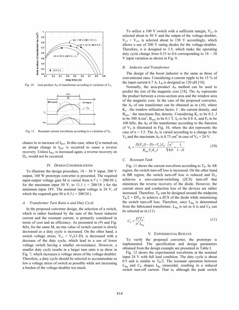
Fig. 10. Area-product AP of transformer according to variation of VS.
Fig. 11. Resonant current waveforms according to a variation of TR.
chance to re-increase of IDo1. In this case, when Q is turned-on, an abrupt change in IDo1 is occurred to cause a reverse recovery. Unless IDo1 is increased again, a reverse recovery on Do1 would not be occurred.
IV. DESIGN CONSIDERATIONS To illustrate the design procedure, 18 ~ 30 V input, 200 V
output, 160 W prototype converter is presented. The required input-output voltage gain M is varied from 6.7 ( = 200/30 ), for the maximum input 30 V, to 11.1 ( = 200/18 ) for the minimum input 18V. The nominal input voltage is 24 V, of which the required gain M is 8.3 ( = 200/24 ).
A. Transformer Turn Ratio n and Duty Cycle
In the proposed converter design, the selection of a switch, which is rather burdened by the sum of the boost inductor current and the resonant current, is primarily considered in terms of cost and an efficiency. As presented in (9) and Fig. 8(b), for the same M, an rms value of switch current is slowly decreased as a duty cycle is increased. On the other hand, a switch voltage stress, Vo1 = VS/(1-D), is decreased with a decrease of the duty cycle, which lead to a use of lower voltage switch having a smaller on-resistance. However, a smaller duty cycle results in a larger turn ratio n as show in Fig. 7, which increases a voltage stress of the voltage-doubler. Therefore, a duty cycle should be selected to accommodate as low a voltage stress of switch as possible while not increasing a burden of the voltage-doubler too much.
To utilize a 100 V switch with a sufficient margin, Vo1 is selected about to 50 V and the output of the voltage-doubler, Vo2 + Vo3, is selected about to 150 V accordingly, which allows a use of 200 V rating diodes for the voltage-doubler. Therefore, n is designed to 3.5, which make the operating duty cycle change from 0.33 to 0.6 corresponding to 18 ~ 30 V input variation as shown in Fig. 9.
B. Inductor and Transformer
The design of the boost inductor is the same as those of conventional ones. Considering a current ripple to be 15 % of the input current 6.7 A, LB is designed as 120 uH [18].
Normally, the area-product AP method can be used to predict the size of the magnetic core [18]. The AP represents the product between a cross-section area and the window area of the magnetic core. In the case of the proposed converter, the AP of one transformer can be obtained as in (10), where Ku : the window utilization factor, J : the current density, and Bmax : the maximum flux density. Considering Ku to be 0.3, J to be 300 A/cm2, Bmax to be 0.1 T, IO to be 0.8 A, and FS to be 100 kHz, the AP of the transformer according to the function of VS is illustrated in Fig. 10, where the dot represents the case of n = 3.5. The AP is varied according to a change in the VS and the maximum AP is 0.73 cm4 in case of VS = 24 V.
( ) 2
max
(1 ) 18 1
O S OP
S u
D V D V IA
B F K J D Dp- -
= +-
(10)
C. Resonant Tank
Fig. 11 shows the current waveform according to TR. In AR region, the switch turn-off loss is increased. On the other hand, in BR region, the switch turn-off loss is reduced and Do2 achieves a zero-current-switching (ZCS) turn-off that minimizes the reverse recovery of the diode. However, the current stress and conduction loss of the devices are rather increased. Therefore, TR can be designed around the midpoint, TR/2 = DTS, to achieve a ZCS of the diode while minimizing the switch turn-off loss. Therefore, once Llkg is determined from the fabricated transformer, Llkg is set as it is and CR can be selected as in (11).
2 2
2S
Rlkg
D TCLp
= (11)
V. EXPERIMENTAL RESULTS To verify the proposed converter, the prototype is
implemented. The specification and design parameters obtained from the design example are presented in Table I.
Fig. 12 shows the experimental waveforms at the nominal input 24 V with full load condition. The duty cycle is about 0.5 and is similar to TR/2. The resonant operation between Llkg and CR shapes Ilkg sinusoidal, resulting in a reduced switch turn-off current. That is, although the peak switch
814
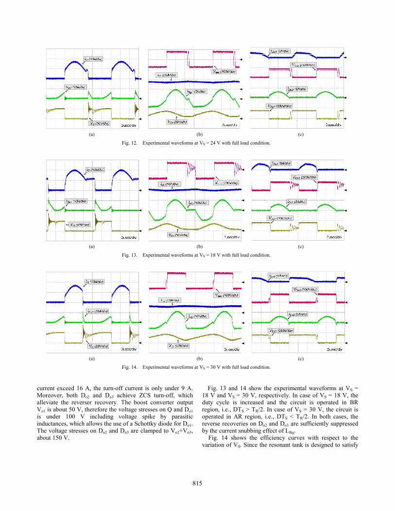
(a) (b) (c)
Fig. 12. Experimental waveforms at VS = 24 V with full load condition.
(a) (b) (c)
Fig. 13. Experimental waveforms at VS = 18 V with full load condition.
(a) (b) (c)
Fig. 14. Experimental waveforms at VS = 30 V with full load condition.
current exceed 16 A, the turn-off current is only under 9 A. Moreover, both Do2 and Do3 achieve ZCS turn-off, which alleviate the reverser recovery. The boost converter output Vo1 is about 50 V, therefore the voltage stresses on Q and Do1 is under 100 V including voltage spike by parasitic inductances, which allows the use of a Schottky diode for Do1. The voltage stresses on Do2 and Do3 are clamped to Vo2+Vo3, about 150 V.
Fig. 13 and 14 show the experimental waveforms at VS = 18 V and VS = 30 V, respectively. In case of VS = 18 V, the duty cycle is increased and the circuit is operated in BR region, i.e., DTS > TR/2. In case of VS = 30 V, the circuit is operated in AR region, i.e., DTS < TR/2. In both cases, the reverse recoveries on Do2 and Do3 are sufficiently suppressed by the current snubbing effect of Llkg.
Fig. 14 shows the efficiency curves with respect to the variation of VS. Since the resonant tank is designed to satisfy
815
Fig. 15. Measured efficiency.
.
the condition DTS = TR/2 at VS = 24 V, the proposed circuit shows the high efficiency over 93 % at this point along a wide load range. In the case of VS = 18 V, an increased conduction loss degrades the efficiency. On the other hand, in the case of VS = 30 V, the operation in AR region increases the switch turn-off loss, though a conduction loss is decreased. Consequently, it is noted that the efficiency is highly affected by the resonant tank design.
Table I
Experimental parameters
Part Value Input voltage VS 18 V ~ 30 V ( nominal input : 24 V )
Output voltage VO 200 V Output Power PO 160 W ( IO = 0.8 A )
Switching frequency FS 100 kHz
Boost inductor LB Inductance = 120 uH, high flux, outer diameter = 27 mm, μ = 125
Transformer turn ratio n 3.5, core : EER28/16/11, AP = 0.91cm4 Transformer leakage
inductance Llkg 2 uH
Balance capacitance CR 1 uF
Switch Q IRF540A ( Rds = 0.052 Ω, VDSS = 100 V )
Diodes
Do1: 16CTQ100 ( VF = 0.58 V, VRRM = 100 V ),
Do2, Do3: 10ETF02 ( VF = 1.2 V, VRRM = 200 V )
VI. CONCLUSION To raise step-up gain of a boost converter further in non-
isolated applications, a voltage-doubler, which is inherently suitable for high voltage applications, is integrated with a boost converter in series as an auxiliary step-up circuit. The voltage-doubler provides an additional step-up ratio on top of the gain of the boost converter and distributes voltage stresses on devices as well. The interface between the boost converter and the voltage-doubler is accomplished by the transformer, which also contribute to a step-up gain by the turn ratio n. The transformer leakage inductance and the balancing capacitor constitute the resonant tank and its resonant operation shapes the current sinusoidal, resulting in a reduced switch turn-off loss and a reverse recovery on diode. Therefore, the proposed converter is promising for high step-up applications with high efficiency. It is also noted that other type of rectifier can also be integrated with a boost converter, being interfaced by a transformer and a balancing capacitor, in the same way to the voltage-doubler.
REFERENCES [1] R. W. Erickson and D. Maksimovic, Fundamentals of Power
electronics, 2nd Ed., John Wiley, New York, USA, 1950, pp. 39-55. [2] K. M. Smith and K. M. Smedly, “Properties and systhesis of passive
lossless soft-switching PWM converters,” IEEE Trans. Power Electronics, vol. 14, no. 5, pp. 890-899, Sep. 1999.
[3] M. M. Jovanovic and Y. Jang, “State-of-the-art, single-phase, active power-factor-correction techniques for high-power applications – an
overview,” IEEE Trans. Industrial Electronics, vol. 52, no. 3, pp. 701-708, Jun. 2005.
[4] F. L. Luo and H. Ye, “Positive output cascade boost converters,” IEE Proc. Electr. Power Appl., vol. 151, no. 5, sep. 2004.
[5] T.-F. Wu, Y.-S. Lai, J.-C. Hung, and Y.-M. Chen, “Boost converter with coupled inductors and buck-boost type of active clamp.” IEEE Trans. Industrial Electronics, vol. 55, no. 1, pp. 154-162, Jan. 2008.
[6] Q. Zhao and F. C. Lee, “High-efficiency, high step-up dc-dc converters.” IEEE Trans. Power Electronics, vol. 18, no. 1, pp. 65-73, Jan. 2003.
[7] K. C. Tseng and T. J. Liang, “Novel high-efficiency step-up converter,” IEE Proc. Electr. Power Appl., vol. 151, no. 2, pp. 182-190, Mar. 2004.
[8] R.-J Wai and R.-Y. Duan, “High step-up converter with coupled-inductor,” IEEE Trans. Power Electronics, vol. 20, no. 5, pp. 1025-1035, Sep. 2005
[9] W. Li and X. He, “A family of interleaved DC-DC converters deduced from a basic cell winding-cross-coupled inductors (WCCIs) for high step-up or step-down converters,” IEEE Trans. Power Electronics, vol. 23, no. 4, pp. 1791-1801, Jul. 2008.
[10] H. Ye and F. L. Luo, “Positive output super-lift converters,” IEEE Trans. Power Electronics, vol. 18, no. 1, pp. 105-113, Jan. 2003.
[11] E. H. Ismail, M. A. Al-Saffar, A. J. Sabzali, and A. A. Fardoun, “A family of single-switch PWM converters with high step-up conversion ratio,” IEEE Trans. Circuit and System I, vol. 55, no. 4, pp. 1159-1171, May 2008.
[12] M. Prudente et al, “Voltage multiplier cells applied to non-isolated DC-DC converters,” IEEE Trans. Power Electronics, vol. 23, no. 2, pp. 871-887, Mar. 2008.
[13] W. C. P. de Aragao Filho and I. Barbi, “A comparison between two current-fed push-pull DC-DC converters – analysis, design and experimentation,” INTELEC, 1996, pp. 313-320.
[14] Y. Jang and M. M. Javanovic, “New two-inductor boost converter with auxiliary transformer,” IEEE Trans. Power Electronics, vol. 19, no. 1, pp. 169-175, Jan. 2004.
[15] K.-B. Park, H.-W. Seong, H.-S. Kim, G.-W. Moon, and M.-J. Youn, "Integrated boost-sepic converter for high step-up applications," in Proc. IEEE PESC, 2008, pp. 944-950.
[16] K.-B. Park, C.-E. Kim, G.-W. Moon, and M.-J. Youn, “"Non-isolated high step-up converter based on boost integrated half-bridge converter," in Proc. INTELEC, 2009, PC13-3.
[17] K.-B. Park, C.-E. Kim, G.-W. Moon, and M.-J. Youn, “PWM resonant single-switch isolated converter,” IEEE Trans. Power Electronics, vol. 24, no. 8, pp. 1876-1886, Aug. 2009.
[18] L. H. Dixon, “Transformer and inductor design for optimum circuit performance,” in Proc. Unitrode Power Supply Design Seminar, 2002.
816
Related Documents