High Speed Line-Scan Machine Vision Perry C. West President Automated Vision Systems, Inc.

Welcome message from author
This document is posted to help you gain knowledge. Please leave a comment to let me know what you think about it! Share it to your friends and learn new things together.
Transcript

High Speed Line-Scan Machine Vision
Perry C. West President
Automated Vision Systems, Inc.

Why This Course?
You will be able to develop high speed, real-time, and line-scan
imaging applications.

You will be able to …
• Tell why latency and determinism are important in machine vision
• Describe what is meant by high speed machine vision
• Describe the difference between soft and hard real time
• Make calculations necessary to design a real-time line-scan vision system
• Describe the basic parts of a line-scan image sensor
• Identify the three ways of making a color line-scan camera

You will be able to …
• Tell why line-scan imaging requires an intense light source
• Identify two shortcomings of common operating systems for high speed, real-time machine vision applications
• State why real-time operating systems are not widely used in machine vision
• Calculate the number of elements needed in a line-scan imager
• Calculate the needed scan rate for a line-scan application

You will be able to …
• Estimate the image processing demands for a line-scan application
• Describe an important characteristic of point-to-point, asynchronous, and isochronous data transmission protocols
• Identify seven current camera interfaces and a principal value of each one
• Identify two different memory buffer approaches
• Tell what to do when memory buffers overflow
• Describe how to restore determinism after image processing is complete

You will be able to …
• Tell a way that line-scan image sensors can be designed to give higher speed
• Describe how TDI improves the sensitivity to light for line-scan imaging
• Identify two approaches to parallel processing and describe how they differ from standard computer architecture
• List at least four ways to improve the performance of image processing

Topics
• Basic concepts • Latency • High speed • Determinism • Real-time
• Work through examples for line-scan imaging • Ruler in space (edge guiding) • Web scanning
• Uniform field • Patterned field
• Bulk conveying/sorting • Ultra-high-resolution imaging • Cylinder periphery

Latency

Latency Example
Event
Latency Minimum
Maximum
A
7
10 B
12
25
C
5
7 Total
24
42

What is High Speed?

High Speed
Associative Comparative

High Speed
1101000100100011101
1101000100100011101
1101000100100011101
1101000100100011101
Image to Result
Image to Image

High Speed Challenge
• Assume: • A 2-D image of dimension MxN (a total of P = M*N pixels) • One image arrives every T seconds • 1/3 T is required for image acquisition
• 1/6 T for exposure • 1/6 T for transmission to the processor
• 2/3 T is available for image processing Perform correlation with a template of size KxK (a total of L = K*K pixels) The number of image processing operations is proportional to M*N*K*K = P*L The processing requirement is proportional to P*L / (2/3 T) = 3*P*L / 2T pixels / second

New Requirement!!!!
The features needing detection are now half their original size! The image must grow to 2Mx2N = 4P Image acquisition time 1/6T for exposure (unchanged) 4/6 T for image transmission time (proportional to number of pixels) 1/6 T available for processing The kernel must grow to 2Kx2K = 4L The number of image processing operations is now proportional to 4P*4L = 16*P*L Image processing time available is 1/6T The image processing rate must be 16*P*L / (1/6 T) = 96*P*L / T The processor must now operate at a rate increase of (96*P*L/T) / (3*P*L / 2T)= 144x

What is Real-Time?

Determinism

Soft Real-Time

Hard Real-Time

Real-Time
High Speed

Summary
• Latency is the start to finish time
• High-speed is in the eye of the beholder
• Based on typical latency
• Real-time is the timeliness of results
• They are on time
• Implemented by limiting the variation in latency (determinism)
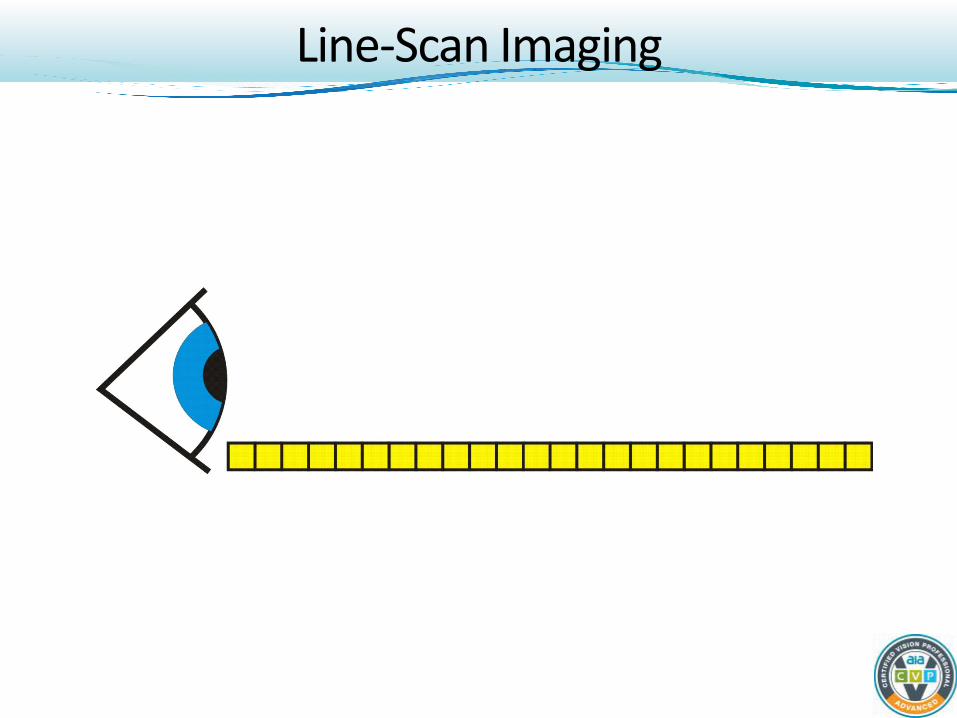
Line-Scan Imaging

Introduction to Line-Scan
Lengths from 128 elements up to 24,576 elements

Extra Sensing Elements

Introduction to Line-Scan

Line-Scan Exposure
Sensing element is a “photon counter” Exposure = photon flux x sensor area x exposure time x quantum efficiency
Area sensor: Assume 1000x1000 pixels 30 fps (33 msec exposure time)
Line-scan sensor: Assume 1000 elements Assume same area and quantum efficiency per sensing element Require same pixel rate Exposure time = 33msec / 1000 = 33usec Photon flux must be 1000 time greater
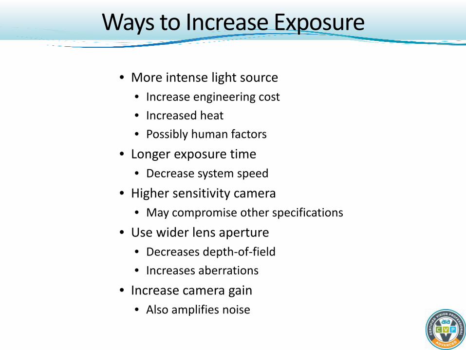
Ways to Increase Exposure
• More intense light source • Increase engineering cost • Increased heat • Possibly human factors
• Longer exposure time • Decrease system speed
• Higher sensitivity camera • May compromise other specifications
• Use wider lens aperture • Decreases depth-of-field • Increases aberrations
• Increase camera gain • Also amplifies noise

Line Light Sources

Color Line-Scan

Summary: Intro to Line-Scan
• A line-scan sensor consists of a single row of sensing elements
• All sensing elements are transferred in parallel to a readout shift register
• The image data is shifted serially out of the readout register
• Requires a much more intense light source • Color line-scan sensors/cameras are available
• Tri-linear • Bayer filter • Three chip

Ruler in Space

Latency Worksheet Latency
Minimum Maximum
a Scan period
b Trigger to output
c Part detector
d Capture command
e Subtotal 1 c + d
f Camera exposure
g Camera to interface
h Interface to RAM
j End-of-frame interrupt
k Image data transfer g + h + j
m Image processing
n Subtotal 2 e + f + k + m
p Resynchronization
q Time base
r Output activation
Total n + p + q + r
Blur (B)
B = fMAX * VP / RS
Pixel data rate (PR)
PR = NP / aMIN

Edge Guiding Requirements
• Opaque web (backlight practical)
• Report the edge position within a range spanning 200mm
• Have an accuracy of .25mm
• Report a measurement every 5 msec
• Interface is 4 to 20mA current loop

Why Line-Scan Imaging?
Why line-scan imaging for edge guiding rather than area imaging? • Simpler image processing • Wider web width accommodation • Higher update rates – more stable control loop

Edge Guiding Challenges
• Web stability (in Z direction) • Tension rollers • Telecentric lens
• Speed • Illumination • Real-time
• Feedback loop stability

Initial Evaluation
• Need to measure 0.25mm accuracy out of 200mm
• Use accuracy to resolution ratio of 10 • No sub-pixel resolution technique employed
• Need to resolve .025mm out of 200mm
• Requires 200mm / .025mm = 8,000 element line-scan camera
• Choose 8,192 element line-scan camera

Interface
• Almost any available interface will work
• Choose 20Mhz pixel clock
• Scan period is 5 msec
• Camera can free run
• Choose IEEE 1394b (FireWire) for lowest cost
• Data transmission latency is 0.227 +0.125/-0 msec • Two 4,196 byte packets + 125µsec between
packets

Image Processing Data Rate
PR is the processing rate (pixels / second)
NP is the number of pixels in each acquired scan
TS is the scan period
.sec/400,638,1/.sec005.
/8192 pixelsscan
scanpixelsTNP
S
PR ===

Latency Worksheet Latency (msec)
Minimum Maximum
a Scan period 5 5
b Trigger to output 5 10
c Part detector Free run Free run
d Capture command n/a n/a
e Subtotal 1 0 0 c + d
f Camera exposure 5 5
g Camera to interface .227 .352
h Interface to RAM
j End-of-frame interrupt
k Image data transfer g + h + j
m Image processing
n Subtotal 2 e + f + k + m
p Resynchronization
q Time base
r Output activation
Total n + p + q + r
Blur (B)
B = fMAX * VP / RS
Pixel data rate (PR)
PR = NP / TS
1,640,000 pixels / sec
From specification – Free running
From array length and IIDC
spec
Blur is a negligible
issue
8192 pixels and 5 msec
Scan period plus processing
time

Operating System
• General purpose
• Modified general purpose
• Real-time
• Kernel only
• None

General Purpose
• Examples
• Windows
• Linux
• Not high-speed
• Not real-time

Modified General Purpose
• Examples
• Embedded Windows
• Windows CE
• Windows with real-time extensions
• Linux with real-time extensions
• Functions impeding speed and determinism eliminated or replaced

Real-Time
• Stand-alone RTOS • Examples
• VTRX • RTXC • QNX • VxWorks
• Mostly for DSP
devices
• Co-resident RTOS • Examples
• InTime • RTX • Kithara
• Coexists with
Windows
Kernel • Examples
– velOSity – DSP/BIOS
• Independent of any
operating system • No HMI support

Hardware Only
• Dedicated processor with no OS or kernel
• PIC
• GPU (Graphics Processing Unit)
• Hardware
• FPGA
• More complex to design
• More difficult to upgrade

Real-Time Characteristics
• Prioritize tasks/threads
• Interrupts
• Preemptive
• Guaranteed latency

Real-Time
•Device driver availability
Real-time operating system’s main barrier to machine vision:

Tuning the Operating System
• Disable virtual memory – have enough RAM to not need it.
• Disable all programs not absolutely necessary. Preferably uninstall and remove them.
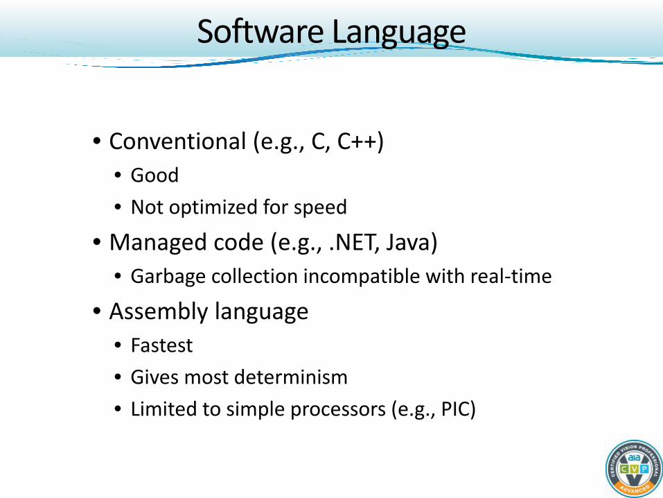
Software Language
• Conventional (e.g., C, C++) • Good • Not optimized for speed
• Managed code (e.g., .NET, Java) • Garbage collection incompatible with real-time
• Assembly language • Fastest • Gives most determinism • Limited to simple processors (e.g., PIC)

Processor Selection
• Considering that the update rate is slow, the processing burden is low, and there is only a need for soft real-time: • Select an inexpensive embedded x86 processor
• Run Windows or Linux
• Program in C, or C++, or another compiled language that does not feature managed code

Edge Guiding Timing

Latency Worksheet Latency (msec)
Minimum Maximum
a Scan period 5 5
b Trigger to output 5 10
c Part detector Free run Free run
d Capture command n/a n/a
e Subtotal 1 0 0 c + d
f Camera exposure 5 5
g Camera to interface .227 .352
h Interface to RAM 0.26 2.4
j End-of-frame interrupt 0 .02
k Image data transfer 0.487 2.772 g + h + j
m Image processing
n Subtotal 2 e + f + k + m
p Resynchronization
q Time base
r Output activation
Total n + p + q + r
Blur (B)
B = fMAX * VP / RS
Pixel data rate (PR)
PR = NP / TS
1,640,000 pixels / sec
Estimates for the PCI
bus Estimates
for end-of-line polling

Latency Worksheet Latency (msec)
Minimum Maximum
a Scan period 5 5
b Trigger to output 5 10
c Part detector Free run Free run
d Capture command n/a n/a
e Subtotal 1 0 0 c + d
f Camera exposure 5 5
g Camera to interface .227 .352
h Interface to RAM 0.26 2.4
j End-of-frame interrupt 0 .02
k Image data transfer 0.487 2.772 g + h + j
m Image processing 0.1 0.7
n Subtotal 2 5.587 8.472 e + f + k + m
p Resynchronization n/a n/a
q Time base n/a n/a
r Output activation 0.7 1.2
Total 6.287 9.672 n + p + q + r
Blur (B)
B = fMAX * VP / RS
Pixel data rate (PR)
PR = NP / TS
1,640,000 pixels / sec
Estimates based on
experience
From interface
card specs

Summary
• Line-scan is usually better than area scan for 1 dimensional ruler-in-space applications
• Update rate must be sufficiently high to insure control loop stability – soft real time
• There are choices in operating systems; often, a general purpose OS is not suitable
• A simple processor can work for lower speed applications

Web Inspection – Clear Field
Defect inspection

Web Inspection -- Specs
• Web width: 670 to 680mm • Web speed: 550mm/sec to 640mm/sec • Find all defects
• Blemishes 1mm or larger • Scratches 10mm or longer
• Defect marking • Inkjet dot • 100mm downstream of camera’s line-of-view • Mark within 2mm of center of defect

Hard Real-Time

Line-Scan Width
Pixels to span minimum defect: 3 pixels
Spatial resolution: 1mm / 3 pixels = 0.33mm/pixel or 0.33mm/scan
Overscan allowance: 5%
Image resolution: (680mm / 0.33mm/pixel) * 1.05
= 2163 elements
Choices: 2048 or 4096 elements
Choose 4096 element line-scan and ignore 1933 pixels (typically 966 each end).

Scan Rate
Desired scan spacing (longitudinal spatial resolution) is the same as lateral spatial resolution – 0.33mm / scan. The scan rate needs to be: 0.33 (mm /scan) / 550 (mm / sec) = 0.600 msec /scan to 0.33 (mm / scan) / 640 (mm / sec) = 0.515 msec / scan A fixed scan rate will make the size of the defects vary in the image. Use an encoder to insure each scan spans the same distance on the surface. Encoder pulses occur 3 per millimeter.

Conveyor Speed Variation

Latency Worksheet Latency (msec scans)
Minimum Maximum
a Scan period 1 1
b Trigger to output 294 306
c Part detector
d Capture command
e Subtotal 1 c + d
f Camera exposure
g Camera to interface
h Interface to RAM
j End-of-frame interrupt
k Image data transfer g + h + j
m Image processing
n Subtotal 2 e + f + k + m
p Resynchronization
q Time base
r Output activation
Total n + p + q + r
Blur (B)
B = TE * VP / RS
100±2 mm and 0.3mm/scan (to center of
defect)
Pixel data rate (PR)
PR = NP / TS
The encoder is the timing generator

Latency Worksheet Latency (scans)
Minimum Maximum
a Scan period 1 1
b Trigger to output 294 306
c Part detector -.004 .004
d Capture command 0 1
e Subtotal 1 -.004 1.004 c + d
f Camera exposure
g Camera to interface
h Interface to RAM
j End-of-frame interrupt
k Image data transfer g + h + j
m Image processing
n Subtotal 2 e + f + k + m
p Resynchronization
q Time base
r Output activation
Total n + p + q + r
Blur (B)
B = TE * VP / RS
Encoder jitter of ±2µsec with
scan times ranging from
515 to 600µsec
Pixel data rate (PR)
PR = NP / TS
The uncertainty
from any point on the web to
the start (center) of a
scan

Variable Scan Time
Consequence:
If exposure time = scan time, and scan time varies
Then exposure time varies
But wait! There’s more ….

Exposure Dynamics

Motion Blur
Exposure time =
Scan time
Zero exposure time
Short exposure time
Choose Exposure Time
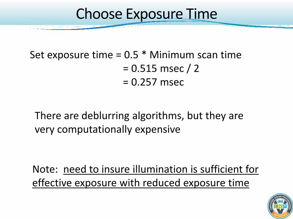
Set exposure time = 0.5 * Minimum scan time = 0.515 msec / 2 = 0.257 msec
Note: need to insure illumination is sufficient for effective exposure with reduced exposure time
There are deblurring algorithms, but they are very computationally expensive

Calculate Blur
Blur = TE * VP / RS = 0.5 scan * 0.33 mm/scan / 0.33 mm/scan = 0.5 scan = 0.17mm TE is exposure time VP is velocity of part RS is spatial resolution

Latency Worksheet Latency (scans)
Minimum Maximum
a Scan period 1 1
b Trigger to output 294 306
c Part detector -.004 .004
d Capture command 0 1
e Subtotal 1 -.004 1.004 c + d
f Camera exposure 0.428 0.5
g Camera to interface
h Interface to RAM
j End-of-frame interrupt
k Image data transfer g + h + j
m Image processing
n Subtotal 2 e + f + k + m
p Resynchronization
q Time base
r Output activation
Total n + p + q + r
Blur (B)
B = TE * VP / RS
0.5 scan (0.17mm)
Pixel data rate (PR)
PR = NP / TS
Exposure is fixed time, but scan time can
vary
From blur calculation

Latency Worksheet Latency (scans)
Minimum Maximum
a Scan period 1 1
b Trigger to output 294 306
c Part detector -.004 .004
d Capture command 0 1
e Subtotal 1 -.004 1.004 c + d
f Camera exposure 0.428 0.5
g Camera to interface
h Interface to RAM
j End-of-frame interrupt
k Image data transfer g + h + j
m Image processing
n Subtotal 2 e + f + k + m
p Resynchronization
q Time base
r Output activation
Total n + p + q + r
Blur (B)
B = TE * VP / RS
0.5 scan (0.17mm)
Pixel data rate (PR)
PR = NP / TS
4,202,000 pixels / second
2164 pixels per scan line from
the frame grabber and 0.515 msec scan period

Pixel Clock
Minimum scan period = 0.516 msec Assume 4096 element camera Pixel clock frequency > # elements / scan period > 4096 / 0.516 msec = 7.94 MHz Pick 20 MHz pixel clock frequency

Interface Choices
Candidates • Camera Link® • GigE Vision® • USB3 VisionTM
• Camera Link HSTM (few camera choices)
• CoaXPress (limited camera choices)
Not considered • Analog (obsolete, unavailable) • LVDS (obsolete, not suitable
for new designs) • FireWire (becoming less used) • USB 2.0 (low bandwidth, not
standardized for machine vision)
Primary considerations • Bandwidth • Latency • Reliability • Software standardization • Cable size • Maximum cable length

Asynchronous
Data Packet 1
Data OK
Data Packet 2
Data Packet 3
Data Not OK

Isochronous
Data Packet

Point-to-Point
101010101010101010101010101010 101010101010101010101010101010 101010101010101010101010101010 101010101010101010101010101010

Interface USB3 VisionTM Camera Link® Camera Link HSTM
GigE Vision® CoaXPress
Bandwidth (based on 8 bit pixels)
400 227 to 680 300 to 6,000 100 775 to 3,000
Determinism Indeterminate Asynchronous
Point-to point, a few camera clock cycles
Point-to point, a few camera clock cycles
Indeterminate Asynchronous
Point-to point, a few camera clock cycles
Reliability Error check and retry
No error check Error check and retry possible
Error check and retry
Error check and retry possible
Software standard
GenIcam Camera Link GenIcam GenIcam GenIcam
Cable length
5 meters 10 meters 15 meters 100 meters 40 meters

Practical Considerations
GigE, Camera Link, and USB 3.0 give the widest camera selection and best performance Camera Link advantages • Speed • Determinism GigE advantages: • Low cost • Simplicity (no frame grabber) • Cable length USB3 advantages: • Low cost • Simplicity (no frame grabber) • Speed For this example, choose Camera Link

Latency Worksheet Latency (scans)
Minimum Maximum
a Scan period 1 1
b Trigger to output 294 306
c Part detector -.004 .004
d Capture command 0 1
e Subtotal 1 -.004 1.004 c + d
f Camera exposure 0.5 0.5
g Camera to interface 0.342 0.398
h Interface to RAM
j End-of-frame interrupt
k Image data transfer g + h + j
m Image processing
n Subtotal 2 e + f + k + m
p Resynchronization
q Time base
r Output activation
Total n + p + q + r
Blur (B)
B = TE * VP / RS
0.5 scan (0.17mm)
20 Mhz camera clock, 4096 element
camera; 0.205 msec
0.515 to 0.600 msec scan
time
Pixel data rate (PR)
PR = NP / TS
4,202,000 pixels / second

Will a PC Work?

Processing Speed
• Processor architecture • Number of cores and their utilization • Clock speed
• Processing speed increases by 37% to 85% of clock speed increase
• Processor support circuits • Memory speed
• Cache • RAM
• Amount of cache memory

Speed
Evaluated by running actual program or benchmark programs

Interface – Frame Grabber

Interrupt Choice
End of line • Better determinism • Lower memory
requirement
End of frame • Less overhead, better
speed • Processing time
flexibility
How many scan lines per frame?
Must be less than 294
Choose a number … 50

Bus Choices
• ISA (obsolete) • PCI
• 132 Mbyte/sec • Determinism uncertain • Requires on-board buffer memory
• PCI-X (limited to server class processors) • Up to 1064 Mbyte/sec • Determinism uncertain • Requires on-board buffer memory
• AGP (obsolete, replaced by PCIe) • PCIe
• x1 – 500 Mbytes/sec • x16 – 8 Gbytes/sec • Latency – virtually zero; direct write to RAM

Latency Worksheet Latency (scans)
Minimum Maximum
a Scan period 1 1
b Trigger to output 294 306
c Part detector -.004 .004
d Capture command 0 1
e Subtotal 1 -.004 1.004 c + d
f Camera exposure 0.5 0.5
g Camera to interface 0.342 0.398
h Interface to RAM 0 50
j End-of-frame interrupt .003 .194
k Image data transfer 0.345 50.592 g + h + j
m Image processing
n Subtotal 2 e + f + k + m
p Resynchronization
q Time base
r Output activation
Total n + p + q + r
Blur (B)
B = TE * VP / RS
0.5 scan (0.17mm)
Use PCIe
Selected “frame” size
Windows estimated latency between 2
to 100µsec
Pixel data rate (PR)
PR = NP / TS
4,202,000 pixels / second

Two Challenges
Is this part of an existing artifact or a
new artifact?
Is this part of an existing artifact or a
new artifact? Which of these is a real defect?

Processing Scheme

Camera Data Buffer

Input Buffer Overflow

Circular Buffer (FIFO)
Guard against output data pointer passing input data pointer (not an error)
Detect input data pointer passing output data pointer -- Error

Interprocess Buffer Overflow

Latency Worksheet Latency (scans)
Minimum Maximum
a Scan period 1 1
b Trigger to output 294 306
c Part detector -.004 .004
d Capture command 0 1
e Subtotal 1 -.004 1.004 c + d
f Camera exposure 0.5 0.5
g Camera to interface 0.342 0.398
h Interface to RAM 0 50
j End-of-frame interrupt .003 .194
k Image data transfer 0.345 50.592 g + h + j
m Image processing 0.1 13
n Subtotal 2 0.941 65.096 e + f + k + m
p Resynchronization
q Time base
r Output activation
Total n + p + q + r
Blur (B)
B = TE * VP / RS
0.5 scan (0.17mm)
From tests or prior experience
Pixel data rate (PR)
PR = NP / TS
4,202,000 pixels / second

Latency Worksheet Latency (scans)
Minimum Maximum
a Scan period 1 1
b Trigger to output 294 306
c Part detector -.004 .004
d Capture command 0 1
e Subtotal 1 -.004 1.004 c + d
f Camera exposure 0.5 0.5
g Camera to interface 0.342 0.398
h Interface to RAM 0 50
j End-of-frame interrupt .003 .194
k Image data transfer 0.345 50.592 g + h + j
m Image processing 0.1 13
n Subtotal 2 0.941 65.096 e + f + k + m
p Resynchronization
q Time base
r Output activation
Total n + p + q + r
Blur (B)
B = TE * VP / RS
0.5 scan (0.17mm)
Pixel data rate (PR)
PR = NP / TS
4,202,000 pixels / second

Resynchronization
A variable, latency dependent, delay created to insures the output does not occur too early

Resynchronization
• Time stamp incoming image
• Result carries time stamp of incoming image
• Result placed in output queue based on time stamp
• Output queue advanced once each time interval

Resynchronization

Time Stamp
• Options • Actual time and date • Frame/scan number (regardless of whether or not
the frame/scan is processed) • Increment of conveyor movement
• Source • Optimal: beginning of exposure • Practical: end-of-frame if time from beginning of
exposure to end-of-frame is deterministic • Scan counter

Resynchronization Considerations
• Minimum latency uncertainty is interval between time events
• The vision system “knows” the time required between input and output
• The vision system must always finish processing relevant image data at least one time interval before the output is needed
• The output queue is usually as long as the number of time intervals between input and output

Latency Worksheet Latency (scans)
Minimum Maximum
a Scan period 1 1
b Trigger to output 294 306
c Part detector -.004 .004
d Capture command 0 1
e Subtotal 1 -.004 1.004 c + d
f Camera exposure 0.5 0.5
g Camera to interface 0.342 0.398
h Interface to RAM 0 50
j End-of-frame interrupt .003 .194
k Image data transfer 0.345 50.592 g + h + j
m Image processing 0.1 13
n Subtotal 2 0.941 65.096 e + f + k + m
p Resynchronization 299 235
q Time base 0 1
r Output activation
Total n + p + q + r
Blur (B)
B = TE * VP / RS
0.5 scan (0.17mm)
Output queue would be at least
306 scans long There is always 1 time period of uncertainty
with the queue
Pixel data rate (PR)
PR = NP / TS
4,202,000 pixels / second
Target trigger to output is 300 scans

Latency Worksheet Latency (scans)
Minimum Maximum
a Image trigger period 1 1
b Trigger to output 294 306
c Part detector -.004 .004
d Capture command 0 1
e Subtotal 1 -.004 1.004 c + d
f Camera exposure 0.5 0.5
g Camera to interface 0.342 0.398
h Interface to RAM 0 50
j End-of-frame interrupt .003 .194
k Image data transfer 0.345 50.592 g + h + j
m Image processing 0.1 13
n Subtotal 2 0.941 scan 65.096 e + f + k + m
p Resynchronization 290 226
q Time base 0 1
r Output activation 5 12.7
Total 295.9 304.8 n + p + q + r
Blur (B)
B = TE * VP / RS
0.5 scan (0.17mm)
The ink jet marker’s latency is from 3 to
7 msec Pixel data rate (PR)
PR = NP / TS
4,202,000 pixels / second
Resynchronization adjusted for
average output latency

Summary
• Scan timing may require external trigger
• When there is motion, there is always a dynamic element that causes blurring
• An early estimate of processing burden can help insure a workable system architecture
• Testing is the only way to know processing speed
• Each camera interface has certain strengths and limitations
• Latency calculations are essential in the design of a high speed or real-time vision system

Summary
• Often scan lines must be grouped together into frames for hardware efficiency
• There are several bus choices, but PCIe is the most popular
• Buffers are commonly used between processes to compensate for short-term variations in processing
• Buffer overflow must be detected
• Resynchronization can restore determinism

High Resolution Imaging

PC Panel Inspection
• Panel size: 18 inches x 24 inches (457.2 x 609.6mm)
• Inspection:
• Compare to master artwork
• Variations in line width or space of .0015 inch (.0381mm) are defects
• Time to inspect: 30 seconds
• Output: digital map of the panel showing defects and locations

Resolution Requirements
• Spatial resolution (RS): .0381mm defect / 3 pixels / defect = .0127mm / pixel
• Pixels to span the panel: • Vertically: 609.6mm / .0127mm / pixel = 48,000 pixels • Horizontally: 457.2mm / .0127mm / pixel = 36,000 pixels
• Total pixels / panel: 48,000 x 36,000 = 1,728,000,000 • Pixel rate: ≥1,728,000,000 pixels / 30 seconds
≥ 57,600,00 pixels / second

Why Not Area Camera(s)?
• High-resolution area cameras cost as much or more than line-scan cameras
• Requires much more image stitching
• Even with multiple high-resolution area cameras, motion is still needed
• Motion must be stopped for area camera exposure – much slower throughput

Initial Design
• Use 8,192 element line-scan camera • Move camera over panel with 5 overlapping swaths • Assume 5% overscan at each edge:
• Each scan lane is 101.6mm wide • RS = 101.6mm / 8192 pixels = .0124mm/pixel
• Assume 3 seconds turn at end of each lane (4 turns) • Actual inspection time is 30 seconds – 4 turns * 3 sec/turn
= 18 seconds
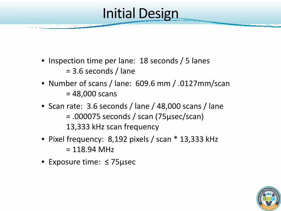
Initial Design
• Inspection time per lane: 18 seconds / 5 lanes = 3.6 seconds / lane
• Number of scans / lane: 609.6 mm / .0127mm/scan = 48,000 scans
• Scan rate: 3.6 seconds / lane / 48,000 scans / lane = .000075 seconds / scan (75µsec/scan) 13,333 kHz scan frequency
• Pixel frequency: 8,192 pixels / scan * 13,333 kHz = 118.94 MHz
• Exposure time: ≤ 75µsec

Single Readout

Dual Readout

Quad Tap Readout

What to Do?
It will be impractical to get enough light intensity into the imaging area. Let’s assume: • It is disadvantageous to use a wider lens aperture. Our options are: • Increase image sensor sensitivity. • Increase exposure time. We can’t do that …. How about TDI (Time Delay and Integration)?
Or can we?

TDI

TDI
• Up to 125 parallel line arrays
• Line timing and part/camera movement must be precisely synchronized
• No electronic shutter possible
• Still have the effect of motion blur

Processing Load
• Each lane has 48,000 scans of 8192 pixels = 393,216,000 pixels
• Require that each lane is processed within 3 seconds of scanning complete -> 131,072,000 pixels/second
• Need more processing power than available in a PC

SISD Processing
SISD – Single Instruction Single Data Examples: • Single core PC • Most embedded processors • DSP

SIMD Processing
SIMD – Single Instruction Multiple Data Examples • Intel MMX/SSE • PowerPC Altivec • Specialized mesh processing chips • Possibly FPGA

MIMD Processing
MIMD – Multiple Instruction Multiple Data Examples • Dedicated circuits (e.g., LUT) • Multicore processor • Arrays of processors • Specialized pipeline processors • One or more dedicated processors working with a general
purpose processor • GPU (Graphic Processing Unit) • FPGA

MIMD Processing

Image Processing Functions
• Preprocessing
• Point transforms
• Neighborhood transforms
• Image transforms
• Segmentation
• Feature extraction
• Interpretation
• Input/output
• General purpose
• Real-time

MIMD
Dedicated Element
FPGA DSP GPU General Purpose
Point Transformation
Excellent Excellent Very good Excellent Very good
Neighborhood Transformation
Excellent to good
Excellent Excellent Excellent Good
Image Transformation
Not appropriate Very good to good
Excellent Very good Very good
Segmentation Not appropriate Fair to poor Excellent Good Excellent
Feature Extraction Not appropriate Good to poor Good Good Excellent
Interpretation Not appropriate Good to poor Good Not appropriate Excellent
General Purpose I/O Not appropriate Good to very good
Fair Not appropriate Excellent
Real-Time I/O Excellent Excellent Fair Not appropriate Poor

Processing Architecture
One processor and buffer memory per
lane
PC consolidates outputs and generates defect map

Instruction Set
• Deterministic instructions minimize latency uncertainty
• Barriers to deterministic instructions
• Instruction pipelining
• Caching
• Efficient processor architecture
• Parallelism (e.g., SSE instructions)

Software Development
• Development tools
• Interactive development environment (IDE)
• Compilers
• Debuggers
• Emulators
• Availability of skilled programmers

Application Software
• Techniques for speed
• Development options
• Techniques for optimization
• Achieving absolute determinism

Techniques for Speed
• Use window (area of interest/ region of interest) to minimize pixels processed
• Processing time α Npixels to Npixels2
• Transfer computationally intensive tasks to hardware
• Algorithm optimization
• Hardware I/O control
• Avoid languages with managed code (e.g., Java, .NET)

Development Options
• Write from scratch • Better code optimization • Longer development time • Need more highly skilled programmers
• Use existing software package
• Faster development • Less optimization • Some packages are not optimized for speed • Most packages do not support real-time

Techniques for Optimization
• Write function specific code
• Design applications to use efficient code
• Use processor’s special functions (e.g., SSE)
• Structure code blocks to be retained in cache
• Avoid complex loops with embedded decisions

Techniques for Optimization
• Use threads and assign priorities
• Use multiple cores or processors
• Use compiler optimization
• Use assembly language where possible/practical
• Avoid allocating memory or creating & destroying objects in time critical routines

Absolute Determinism
• Processing time (per pixel) equals pixel clock period
• Requires zero uncertainty in processing speed
• Processing time not image content dependent
• Difficult to develop and maintain

Tips for Image Processing
• Manage the hardware carefully: optimize
• Cache, RAM, support chips, cores
• Avoid data path bandwidth limitations
• Use a faster computer
• Overlap image acquisition and image processing
• Use regions of interest
• Align data in memory
• Use vector processing (e.g., SSE)
• Create efficient software
• Simplify the image

Simplify the Image
• Repeatable number, location, and orientation of features
• High contrast
• Low noise

Summary
• Multi-tapped sensors can give very high readout rates
• TDI sensors help increase the camera’s sensitivity in high-speed applications
• There are two common forms of parallel processing: SIMD and MIMD
• Absolute determinism is difficult or impossible to achieve
• It is possible to build a vision system that will meet almost any speed demand

We Have Covered …
• Why latency and determinism are important in machine vision
• What is meant by high speed machine vision
• The difference between soft and hard real time
• Calculations necessary to design a real-time line-scan vision system
• The basic parts of a line-scan image sensor
• Three ways of making a color line-scan camera
• Why line-scan imaging requires an intense light source

We Have Covered …
• Shortcomings of common operating systems for high speed, real-time machine vision applications
• Why real-time operating systems are not widely used in machine vision
• How to calculate the number of elements needed in a line-scan imager
• How to calculate the needed scan rate for a line-scan application
• How to estimate the image processing demands for a line-scan application

We Have Covered …
• The important characteristic of point-to-point, asynchronous, and isochronous data transmission protocols
• Seven current camera interfaces and a principal value of each one
• Two different memory buffer approaches
• What to do when memory buffers overflow
• How to restore determinism after image processing is complete
• How line-scan image sensors can be designed to give higher speed

We Have Covered …
• How TDI improves the sensitivity to light for line-scan imaging
• Two common approaches to parallel processing and how they differ from standard computer architecture
• Ways to improve the performance of image processing

Perry C. West President
Automated Vision Systems, Inc. 4787 Calle de Lucia San Jose, California 95124 U.S.A.
Phone: +1 408-267-1746 Email: [email protected]
www.autovis.com
Related Documents
![[MANUALBOOK][FSYT-2 WEATHERPROOF ...Scan Line scan CCD 1/4″SONY CCD Line Scan 15.625KHz Site Scan 50Hz Pixel 795(H) x 596(V) Lens High performance /23X optic zoom / auto focus](https://static.cupdf.com/doc/110x72/604e3b7371163021ed0ab427/manualbookfsyt-2-weatherproof-scan-line-scan-ccd-14asony-ccd-line-scan.jpg)