3 4 1 INTRODUCTION The design considerations for high-speed data conversion are, in many ways, similar to those for data conversion in general. High speed circuits may sometimes seem different because device types can be limited and only certain design techniques and architectures can be used with success. But the basics are the same. High speed circuits or systems are really those that tend to press the limits of state-of-the-art dynamic performance. This bulletin focuses on the more fundamental building blocks such as op amps, sample/holds, digital to analog and analog to digital converters (DACs and ADCs). It concludes with test techniques. Op amps, which tend to be the basic building blocks of systems, are be considered first. Sample/ holds which play an important role in data conversion are considered next followed by DACs and finally ADCs. ADCs are really a combination of the other three circuits. Emphasis is given to hybrid and monolithic design techniques since, in practice, the highest levels of performance are achieved using these processes. The material is presented from a design perspective. Theory and practical examples are of- fered so both the data conversion component designer and user will find the material useful. The concepts presented do not require extensive experience with data conversion. Fun- damental concepts are discussed allowing the subject to be understood easily. The material emphasizes high speed cir- cuit considerations—circuit theory is not treated in depth. Topics Covered in this Bulletin A. Amplifier Architectures 1. Buffer 2. Operational 3. Open Loop 4. Comparator B. Amplifier Applications 1. Sample/Hold 2. Peak Detector C. Digital to Analog Converters 1. Bipolar 2. Deglitched DAC D. Analog to Digital Converters 1. Successive Approximation 2. Flash 3. Sub-ranging E. Test Techniques 1. Settling Time 2. Aperture Jitter 3. Beat Frequency Testing 4. Servo Loop Test AMPLIFIER ARCHITECTURES Amplifiers of all types play an important role in data conversion systems. Since high speed amplifiers are both useful and difficult to design, an understanding of their operation is important. Four different types of amplifier architectures will be discussed. Buffers, op amps, open loop amplifiers, and comparators can be found in just about any signal processing application. THE BUFFER The open loop buffer is the ubiquitous modern form of the emitter follower. This circuit is popular because it is simple, low cost, wide band, and easy to apply. The open loop buffer is important in high speed systems. It serves the same purpose as the voltage follower in lower speed systems. It is often used as the output stage of wideband op amps and other types of broadband amplifiers. Consider the two buffer circuit diagrams, Figures 1 and 2. The output impedance of each buffer is about 5Ω and bandwidths of several hundred megahertz can be achieved. The FET buffer is usually implemented in hybrid form as very wideband FETs and transistors are usually not available on the same monolithic process. The all-bipolar form of the buffer is capable of FIGURE 1. High Speed Bipolar Buffer. V IN V OUT R 4 R 3 Q 4 Q 3 R 2 Q 2 V– V+ Q 1 R 1 R 6 R 5 Q 6 Q 5 V BIAS1 V BIAS2 HIGH SPEED DATA CONVERSION By Mike Koen (602) 746-7337 11 © 1991 Burr-Brown Corporation AB-027A Printed in U.S.A. June, 1991 ® SBAA045

Welcome message from author
This document is posted to help you gain knowledge. Please leave a comment to let me know what you think about it! Share it to your friends and learn new things together.
Transcript
3
4
1INTRODUCTION
The design considerations for high-speed data conversionare, in many ways, similar to those for data conversion ingeneral. High speed circuits may sometimes seem differentbecause device types can be limited and only certain designtechniques and architectures can be used with success. Butthe basics are the same. High speed circuits or systems arereally those that tend to press the limits of state-of-the-artdynamic performance.
This bulletin focuses on the more fundamental buildingblocks such as op amps, sample/holds, digital to analog andanalog to digital converters (DACs and ADCs). It concludeswith test techniques. Op amps, which tend to be the basicbuilding blocks of systems, are be considered first. Sample/holds which play an important role in data conversion areconsidered next followed by DACs and finally ADCs. ADCsare really a combination of the other three circuits. Emphasisis given to hybrid and monolithic design techniques since, inpractice, the highest levels of performance are achievedusing these processes. The material is presented from adesign perspective. Theory and practical examples are of-fered so both the data conversion component designer anduser will find the material useful. The concepts presented donot require extensive experience with data conversion. Fun-damental concepts are discussed allowing the subject to beunderstood easily. The material emphasizes high speed cir-cuit considerations—circuit theory is not treated in depth.
Topics Covered in this Bulletin
A. Amplifier Architectures1. Buffer2. Operational3. Open Loop4. Comparator
B. Amplifier Applications1. Sample/Hold2. Peak Detector
C. Digital to Analog Converters1. Bipolar2. Deglitched DAC
D. Analog to Digital Converters1. Successive Approximation2. Flash3. Sub-ranging
E. Test Techniques1. Settling Time2. Aperture Jitter3. Beat Frequency Testing4. Servo Loop Test
AMPLIFIER ARCHITECTURES
Amplifiers of all types play an important role in dataconversion systems. Since high speed amplifiers are bothuseful and difficult to design, an understanding of theiroperation is important. Four different types of amplifierarchitectures will be discussed. Buffers, op amps, open loopamplifiers, and comparators can be found in just about anysignal processing application.
THE BUFFER
The open loop buffer is the ubiquitous modern form of theemitter follower. This circuit is popular because it is simple,low cost, wide band, and easy to apply. The open loop bufferis important in high speed systems. It serves the samepurpose as the voltage follower in lower speed systems. It isoften used as the output stage of wideband op amps andother types of broadband amplifiers. Consider the two buffercircuit diagrams, Figures 1 and 2. The output impedance ofeach buffer is about 5Ω and bandwidths of several hundredmegahertz can be achieved. The FET buffer is usuallyimplemented in hybrid form as very wideband FETs andtransistors are usually not available on the same monolithicprocess. The all-bipolar form of the buffer is capable of
FIGURE 1. High Speed Bipolar Buffer.
VIN VOUT
R4
R3
Q4
Q3
R2
Q2
V–
V+
Q1
R1
R6
R5
Q6
Q5
VBIAS1
VBIAS2
HIGH SPEED DATA CONVERSIONBy Mike Koen (602) 746-7337
11
©1991 Burr-Brown Corporation AB-027A Printed in U.S.A. June, 1991
®
SBAA045
2
being produced on a complementary monolithic processwhere both the NPN and PNP transistors are high perfor-mance vertical structures. Figure 1 shows the buffer in itsmost basic form. The input to the buffer is connected to apair of complementary transistors. Each transistor is biasedby a separate current source. The input transistors Q1 and Q2
through resistors R1 and R2 are connected to the bases ofoutput transistors Q3 and Q4 so that offset will be zero if thebase to emitter voltage of the NPN and PNP are equal. Zerooffset requires that transistor geometries are designed forequal VBEs at the same bias current—achievable in a comple-mentary process. This circuit is very useful as it has amoderately high input impedance and the ability to supplyhigh current outputs. One important use of this buffer circuitis to amplify the output current of a monolithic op amp.Monolithic op amps usually do not have output currents thatexceed 10mA to 50mA, while the buffer shown in Figure 1is capable of putting out more than 100mA. Typically thistype of a buffer has a bandwidth of 250MHz, allowing it tobe used in the feedback loop of most monolithic op ampswith minimal effect on stability. Figure 3 shows how theloop is closed around the buffer so that the DC performanceof the amplifier is determined by the unbuffered amplifierand not the output buffer. An advantage of the connectionshown in Figure 3 is that load-driving heat dissipating is inthe buffer so that thermally induced distortion and offsetdrift is removed from the sensitive input op amp.
Figure 2 shows the FET version of the previously mentionedcircuit. The FET buffer achieves zero offset by the mirroraction of the NPN transistor Q5 that is reflected as the gate
R2
Op Amp Buffer
R1
VIN
VOUT
A1 A2
FIGURE 3. High Current Op Amp.
FIGURE 2. High Speed FET Buffer.
to source voltage of the input FET Q1. The VBE of Q5
determines the gate to source voltage of the FET currentsource Q4. Since the identical current flows in Q4 and Q1 thegate to source voltage of Q1 will also be equal to VBE. SinceQ5 and Q6 are identical transistors the offset of the FETbuffer circuit will be nominally zero. The circuit shown inFigure 2 is usually constructed in hybrid form so that it isusually necessary to adjust resistors R1 and R2 to set theoffset of this circuit to zero. Setting the offset to zero isaccomplished by laser-trimming resistors R1 and R2 with thebuffer under power. (This is known as active trimming.) Acommon application of this circuit is to buffer the holdcapacitor in a sample/hold. (See the section on sample/holds.) The high impedance of the FET buffer allows thecapacitor to retain the sample voltage for a comparativelylong time as the room temperature input current of a typicalFET is in the vicinity of 50pA.
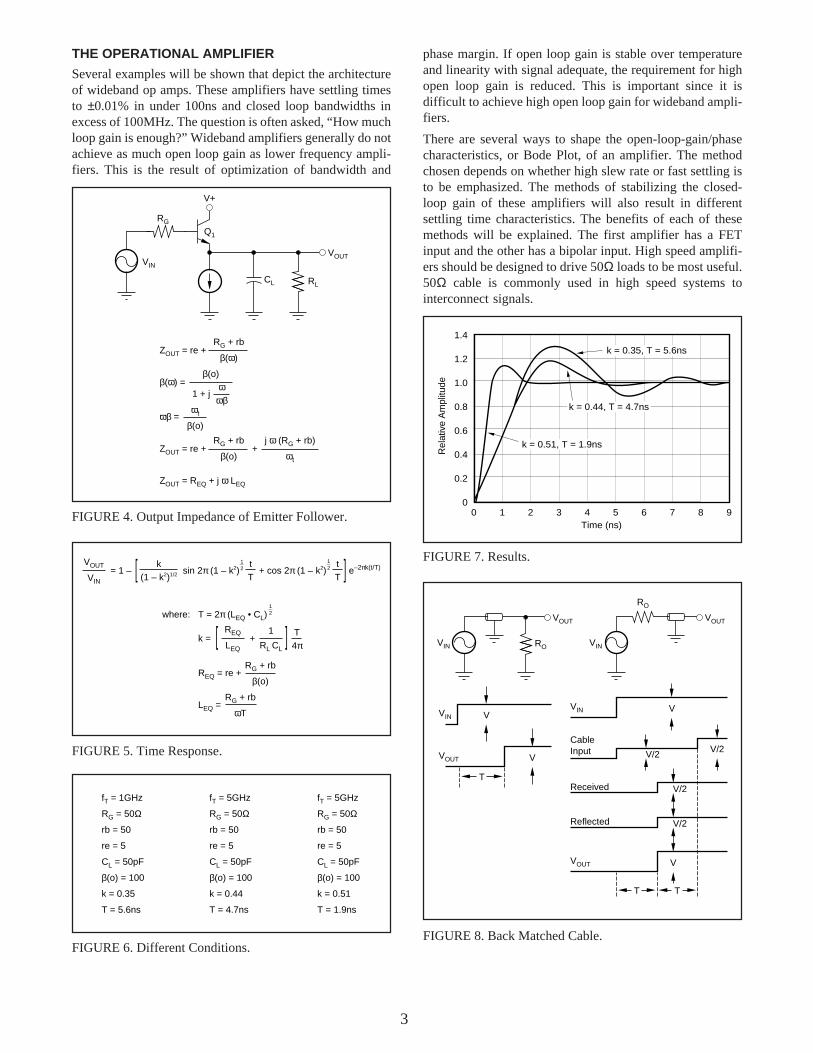
Another common application of either type of buffer circuitis to drive high capacitive loads without reducing the overallsystem bandwidth. Op amps, even though they have closedloop output impedances that are very low, can becomeunstable in the presence of high capacitive loads. The openloop buffer is usually more stable when driving capacitiveloads, but this circuit will also develop a tendency to ring ifthe capacitive load becomes excessive. Figure 4 shows howthe emitter follower can oscillate due to reactive outputimpedance. Figures 5 through 7 show calculated results fordifferent conditions when a simple emitter follower is driv-ing a capacitive load which illustrates this oscillatory ten-dency.
One very important application of the open loop buffer is todrive a “back matched” transmission cable. Back matchinga cable is just as effective in preventing reflections as themore conventional method of terminating the cable at thereceiving end. The advantage of the back matched cable isthat the generating circuit does not have to supply steady-state current and there is no loss of accuracy due to thetemperature dependent copper loss of the cable. Figure 8shows circuit diagrams and explanations that describe theoperation of the open loop buffer driving a “back matched”cable.
V–
VOUT
R3
R4
Q6
Q7
R1
VBE
+–
R2
Q5
VBE
+
–
VGS+
–
Q4
Q3
Q2
VIN Q1
V+
3
phase margin. If open loop gain is stable over temperatureand linearity with signal adequate, the requirement for highopen loop gain is reduced. This is important since it isdifficult to achieve high open loop gain for wideband ampli-fiers.
There are several ways to shape the open-loop-gain/phasecharacteristics, or Bode Plot, of an amplifier. The methodchosen depends on whether high slew rate or fast settling isto be emphasized. The methods of stabilizing the closed-loop gain of these amplifiers will also result in differentsettling time characteristics. The benefits of each of thesemethods will be explained. The first amplifier has a FETinput and the other has a bipolar input. High speed amplifi-ers should be designed to drive 50Ω loads to be most useful.50Ω cable is commonly used in high speed systems tointerconnect signals.
ZOUT = re +
β(ω) =β(o)
ωβ =ωt
β(o)
RG
RG + rb
β(ω)
1 + jω
ωβ
ZOUT = re +
ZOUT = REQ + j ω LEQ
RG + rb
β(o)+
j ω (RG + rb)
ωt
VIN
VOUT
RLCL
V+
Q1
FIGURE 4. Output Impedance of Emitter Follower.
= 1 –VOUT
VIN[ k
(1 – k2)1/2 sin 2π (1 – k2)tT
+ cos 2π (1 – k2)tT ]
where: T = 2π (LEQ • CL)
k =T4π
REQ
LEQ
1
RL CL
+
REQ = re +
LEQ =
RG + rb
β(o)
RG + rb
ωT
12
12
12
[ ]
e–2πk(t/T)
FIGURE 5. Time Response.
fT = 1GHz
RG = 50Ω
rb = 50
re = 5
CL = 50pF
β(o) = 100
k = 0.35
T = 5.6ns
fT = 5GHz
RG = 50Ω
rb = 50
re = 5
CL = 50pF
β(o) = 100
k = 0.44
T = 4.7ns
fT = 5GHz
RG = 50Ω
rb = 50
re = 5
CL = 50pF
β(o) = 100
k = 0.51
T = 1.9ns
FIGURE 6. Different Conditions.
THE OPERATIONAL AMPLIFIER
Several examples will be shown that depict the architectureof wideband op amps. These amplifiers have settling timesto ±0.01% in under 100ns and closed loop bandwidths inexcess of 100MHz. The question is often asked, “How muchloop gain is enough?” Wideband amplifiers generally do notachieve as much open loop gain as lower frequency ampli-fiers. This is the result of optimization of bandwidth and
FIGURE 7. Results.
Time (ns)0 1 2 3 4 5 6 7 8 9
1.4
1.2
1.0
0.8
0.6
0.4
0.2
0
Rel
ativ
e A
mpl
itude
k = 0.35, T = 5.6ns
k = 0.44, T = 4.7ns
k = 0.51, T = 1.9ns
FIGURE 8. Back Matched Cable.
RO
VIN RO
VOUT
VIN V
VOUT V
T
VIN
VOUT
VIN V
VOUT V
T T
Reflected V/2
Received V/2
CableInput V/2 V/2
4
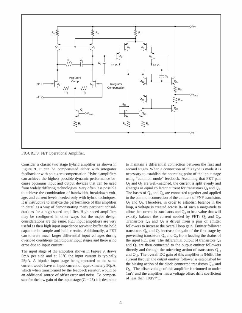
Consider a classic two stage hybrid amplifier as shown inFigure 9. It can be compensated either with integratorfeedback or with pole-zero compensation. Hybrid amplifierscan achieve the highest possible dynamic performance be-cause optimum input and output devices that can be usedfrom widely differing technologies. Very often it is possibleto achieve the combination of bandwidth, breakdown volt-age, and current levels needed only with hybrid techniques.It is instructive to analyze the performance of this amplifierin detail as a way of demonstrating many pertinent consid-erations for a high speed amplifier. High speed amplifiersmay be configured in other ways but the major designconsiderations are the same. FET input amplifiers are veryuseful as their high input impedance serves to buffer the holdcapacitor in sample and hold circuits. Additionally, a FETcan tolerate much larger differential input voltages duringoverload conditions than bipolar input stages and there is noerror due to input current.
The input stage of the amplifier shown in Figure 9, draws5mA per side and at 25°C the input current is typically25pA. A bipolar input stage being operated at the samecurrent would have an input current of approximately 50µA,which when transformed by the feedback resistor, would bean additional source of offset error and noise. To compen-sate for the low gain of the input stage (G = 25) it is desirable
to maintain a differential connection between the first andsecond stages. When a connection of this type is made it isnecessary to establish the operating point of the input stageusing “common mode” feedback. Assuming that FET pairQ2 and Q3 are well-matched, the current is split evenly andemerges as equal collector current for transistors Q4 and Q5.The bases of Q4 and Q5 are connected together and appliedto the common connection of the emitters of PNP transistorsQ8 and Q9. Therefore, in order to establish balance in theloop, a voltage is created across R7 of such a magnitude toallow the current in transistors and Q4 to be a value that willexactly balance the current needed by FETs Q2 and Q3.Transistors Q8 and Q9 a driven from a pair of emitterfollowers to increase the overall loop gain. Emitter followertransistors Q6 and Q7 increase the gain of the first stage bypreventing transistors Q8 and Q9 from loading the drains ofthe input FET pair. The differential output of transistors Q8
and Q9 are then connected to the output emitter followersdirectly and through the mirroring action of transistors Q12
and Q13. The overall DC gain of this amplifier is 94dB. Thecurrent through the output emitter follower is established bythe biasing action of the diode connected transistors Q10 andQ11. The offset voltage of this amplifier is trimmed to under1mV and the amplifier has a voltage offset drift coefficientof less than 10µV/°C.
FIGURE 9. FET Operational Amplifier.
VBIAS
Q4
R5
Q1
R1
R2
–In
+In Q2
Q5
R6
R3
Q3
Pole-ZeroComp
R9
R7
Q8 Q9
Q6 Q7
To V– To V–
Q10
Q11
Q12
Q13
R9R8
V–
V+
IntegratorCompensation
Q15
R10
R11
Q14
VOUT
C1C2
C3

5
The second architecture that will be discussed is known asthe folded cascode operational amplifier. This circuit ar-rangement is very useful as all the open loop gain isachieved in a single stage. Since all of the gain is developedin a single stage, higher usable gain bandwidth product willresult as the Bode Plot will tend to look more like a singlepole response which implies greater stability.
Figure 17 shows a simplified schematic of this type ofamplifier. The input terminals of this amplifier are the basesof transistors Q1 and Q2. The output of transistors Q1 and Q2
are taken from their respective collectors and applied to theemitters of the common base PNPs Q4 and Q5. TransistorsQ4 and Q5 act as cascode devices reducing the impedance at
FIGURE 10. Integrator Compensation.
VOUT
V+
V–
+In–In
G =1β
Aβ1 + Aβ
A(ω) =A(o)
1 + j( ωω1 ) 1 + j( ω
ω2 )Pole
Due toIntegrator
SecondPole
I2I1
C2
A1C1
Q1 Q2
Q3
Q4
FIGURE 11. Transient Response Integrator Compensation.
G =
1 –
1β
where ωn = A(o) β ω1ω2
ζ =
(
ω1 + ω2
2 A(o) β ω1ω2
1
ω2
A(o) β ω1ω2+ j
ωA(o) β
1ω1
1ω2
+
G =
1 –
1β
1
ω2
ωn2+ 2ζ
ωωn
Step Response:
e0(t) =1β
t–ζωnt
1 – ζ2e1(t) 1 – sin (ωn 1 – ζ2 t + cos–1 ζ)
)
( )
[ ]
FIGURE 12. Open Loop Gain, Closed Loop Gain, and Tran-sient Response Integrator Compensation.
Case 2
Aβ
f11 f12 f2
Case 2Case 1
Case 1ζ = 0.2
Case 2ζ = 0.8
GTCase 2
Case 1
eO(t)Case 1
f
f
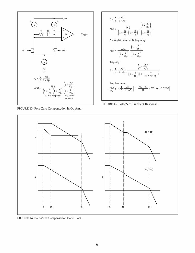
As previously mentioned, there are two methods for com-pensating the open loop frequency response of this ampli-fier. The first method to be discussed is called integratorfeedback as a capacitor is connected from the output stage tothe drain of the input stage. Figure 10 shows a block diagramof this connection which more clearly demonstrates why itis called integrator compensation as an integrator is formedaround the output gain stage of the amplifier. The advantageof integrator feedback is that the closed loop frequencyresponse has all the poles in the denominator which meansthat the transient response is tolerant to parameter variation.As will be shown, another type of frequency compensationis called “doublet” or “pole-zero cancellation” which canhave poor transient response due to small parameter varia-tions. Another benefit of integrator feedback is lower noiseoutput as the integrator forms an output filter as contrastedto pole-zero cancellation which only forms an incompletefilter of the input stage. Figures 11 and 12 show the relation-ship between the frequency and time or transient response ofa feedback amplifier that employs integrator feedback.
Figures 13 through 16 illustrate the effect of a pole-zeromismatch. A pole-zero mismatch creates a “tail” or a longtime constant settling term in the transient response. Pole-zero compensation is not as effective as integrator feedbackin stabilizing an amplifier but should be considered as thereare times when the integrator itself can become unstable.Pole-zero compensated amplifiers often have higher slewrates.
6
FIGURE 13. Pole-Zero Compensation in Op Amp.
V+
V–
+In–In
G =1β
Aβ1 + Aβ
A(ω) =A(o)
1 +( Sω1
)2-Pole Amplifier Pole-Zero
Network
VOUT
1 +( Sω1
) 1 +( Sω0
)1 +( S
ω1' )
Q2Q1
R1 C1A1
I1 I2
FIGURE 15. Pole-Zero Transient Response.
A
ω0 ω1 ω2
A
A
ω0 ω1 ω2
A
ω1 < ω1'
ω1 > ω1'
FIGURE 14. Pole-Zero Compensation Bode Plots.
G =1β
(
Aβ1 + Aβ
Sω1
1 +
A(ω) =A(o)
Step Response:
(t) =1β
ω1' – ω1
ω11 –
)
[ ]
( Sω2
1 + ) ( Sω0
1 + )( S
ω1'1 + )
For simplicity assume A(o) ω0 >> ω2.
( Sω1
1 +
A(ω) =A(o)
) ( Sω0
1 + )( S
ω1'1 + )
If ω1 ≈ ω1' :
G =1β
Aβ1 + Aβ ( S
(1 + Aβ) ω01 + )
( Sω1'
1 + )( S
ω1'1 + )
eOUT
eIN
Aβ1 + Aβ
e–ω1t – e–(1 + Aβ) ω0t
7
FIGURE 16. Pole-Zero Transient Response and Pole-ZeroMismatch.
(t) =1β
1 – e–(1 + Aβ) ω0t –[ ]eOUT
eIN
Aβ1 + Aβ
ω1' – ω1
ω1e–ω1t
ω1' – ω1
ω1e–ω1t
1 – e–(1 + Aβ) ω0t( )
“Tail”
can be stabilized with a single capacitor thereby approximat-ing a single pole response without a settling “tail.”
COMPARATOR
The comparator is a common element in a signal processingsystem and it is used to sense a level and then generate adigital signal, either a “1” or a “0,” to report the result of thatcomparison to the rest of the system. Comparators can beimplemented two different ways, either using a high gainamplifier or by using the latching type approach. Each typeof comparator has advantages as will now be explained.
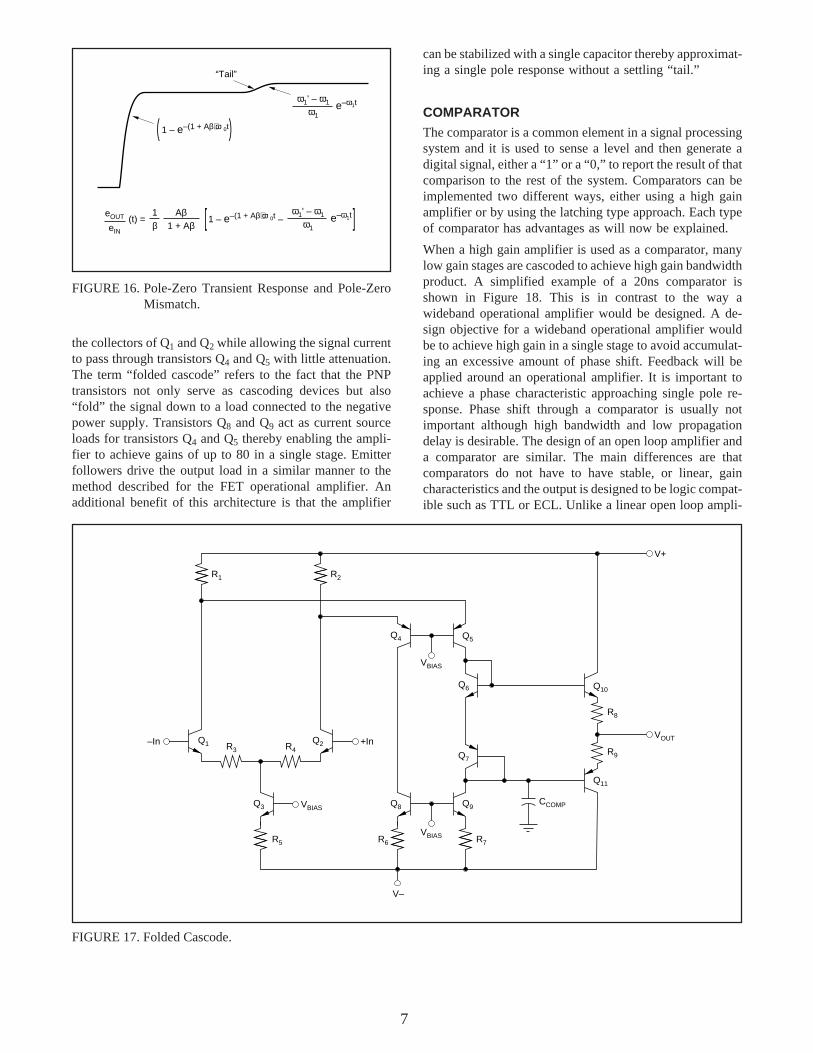
When a high gain amplifier is used as a comparator, manylow gain stages are cascoded to achieve high gain bandwidthproduct. A simplified example of a 20ns comparator isshown in Figure 18. This is in contrast to the way awideband operational amplifier would be designed. A de-sign objective for a wideband operational amplifier wouldbe to achieve high gain in a single stage to avoid accumulat-ing an excessive amount of phase shift. Feedback will beapplied around an operational amplifier. It is important toachieve a phase characteristic approaching single pole re-sponse. Phase shift through a comparator is usually notimportant although high bandwidth and low propagationdelay is desirable. The design of an open loop amplifier anda comparator are similar. The main differences are thatcomparators do not have to have stable, or linear, gaincharacteristics and the output is designed to be logic compat-ible such as TTL or ECL. Unlike a linear open loop ampli-
the collectors of Q1 and Q2 while allowing the signal currentto pass through transistors Q4 and Q5 with little attenuation.The term “folded cascode” refers to the fact that the PNPtransistors not only serve as cascoding devices but also“fold” the signal down to a load connected to the negativepower supply. Transistors Q8 and Q9 act as current sourceloads for transistors Q4 and Q5 thereby enabling the ampli-fier to achieve gains of up to 80 in a single stage. Emitterfollowers drive the output load in a similar manner to themethod described for the FET operational amplifier. Anadditional benefit of this architecture is that the amplifier
FIGURE 17. Folded Cascode.
VBIASQ3
V–
V+
Q11
Q10
VOUT+InQ2–In Q1
Q8 Q9
VBIAS
Q4 Q5
VBIAS
Q6
Q7
CCOMP
R1 R2
R3 R4
R5 R7R6
R8
R9
8
–In+In
VBIAS
V+
LogicOut
V–
ToV+
I3I2I1 I4
R11
R10
R8
R9
R7
R5
R6
R4
R2
R3
R1
I6
I5
Q16
Q15Q14
Q12Q11
Q10
Q13
Q9
Q6
Q8Q7
Q5
Q3 Q4
Q2Q1
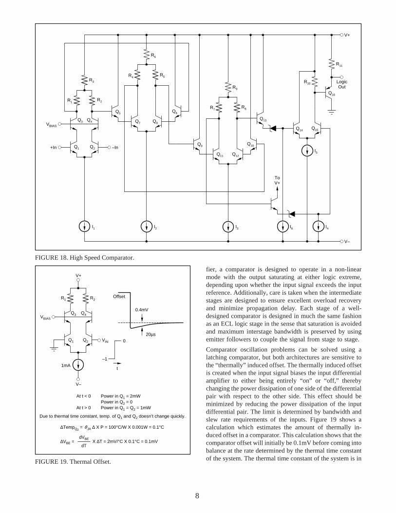
FIGURE 18. High Speed Comparator.
fier, a comparator is designed to operate in a non-linearmode with the output saturating at either logic extreme,depending upon whether the input signal exceeds the inputreference. Additionally, care is taken when the intermediatestages are designed to ensure excellent overload recoveryand minimize propagation delay. Each stage of a well-designed comparator is designed in much the same fashionas an ECL logic stage in the sense that saturation is avoidedand maximum interstage bandwidth is preserved by usingemitter followers to couple the signal from stage to stage.
Comparator oscillation problems can be solved using alatching comparator, but both architectures are sensitive tothe “thermally” induced offset. The thermally induced offsetis created when the input signal biases the input differentialamplifier to either being entirely “on” or “off,” therebychanging the power dissipation of one side of the differentialpair with respect to the other side. This effect should beminimized by reducing the power dissipation of the inputdifferential pair. The limit is determined by bandwidth andslew rate requirements of the inputs. Figure 19 shows acalculation which estimates the amount of thermally in-duced offset in a comparator. This calculation shows that thecomparator offset will initially be 0.1mV before coming intobalance at the rate determined by the thermal time constantof the system. The thermal time constant of the system is inFIGURE 19. Thermal Offset.
Due to thermal time constant, temp. of Q1 and Q2 doesn’t change quickly.
∆TempQ2 = JA ∆ X P = 100°C/W X 0.001W = 0.1°C
VBIAS
1mA
V–
V+
Q2Q1
–1
0
t
Offset
0.4mV
20µs
∆VBE = X ∆T = 2mV/°C X 0.1°C = 0.1mVdVBE
dT
At t < 0
At t > 0
Power in Q1 = 2mWPower in Q2 = 0Power in Q1 = Q2 = 1mW
θ
R2R1
VIN
Q3 Q4
9
V+
RL
V–
VIN
777
VL
Gain* =RL
re
RL
0.026I
=VL
0.026=
* 3rd Stage
Since the gain is proportional to I, a 43dB gain reduction occurs when:
I
I @ BalanceI @ Unbalance
= 141
I @ BalanceI @ Unbalance
= 129mV∆VBE = 26 ln
∆VBE
73=VOVERDRIVE =
129
73= 375µV
Overdrive for 43dB gain reduction:
VO
A1 A2 A3 Q1 Q2
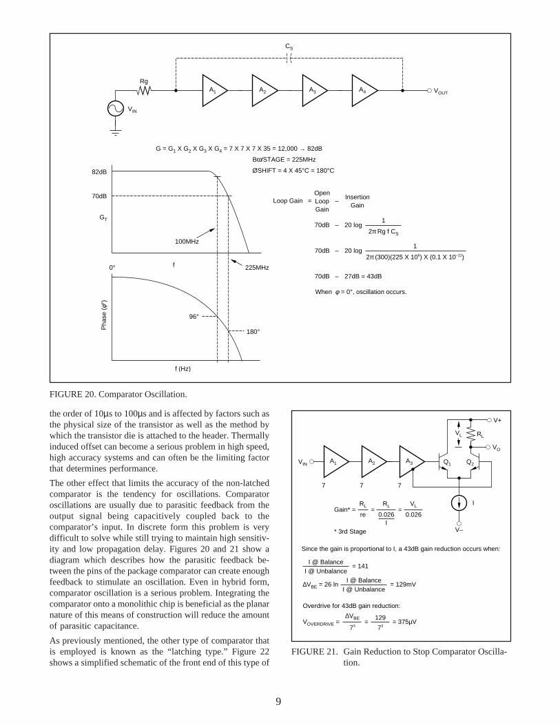
FIGURE 20. Comparator Oscillation.
FIGURE 21. Gain Reduction to Stop Comparator Oscilla-tion.
the order of 10µs to 100µs and is affected by factors such asthe physical size of the transistor as well as the method bywhich the transistor die is attached to the header. Thermallyinduced offset can become a serious problem in high speed,high accuracy systems and can often be the limiting factorthat determines performance.
The other effect that limits the accuracy of the non-latchedcomparator is the tendency for oscillations. Comparatoroscillations are usually due to parasitic feedback from theoutput signal being capacitively coupled back to thecomparator’s input. In discrete form this problem is verydifficult to solve while still trying to maintain high sensitiv-ity and low propagation delay. Figures 20 and 21 show adiagram which describes how the parasitic feedback be-tween the pins of the package comparator can create enoughfeedback to stimulate an oscillation. Even in hybrid form,comparator oscillation is a serious problem. Integrating thecomparator onto a monolithic chip is beneficial as the planarnature of this means of construction will reduce the amountof parasitic capacitance.
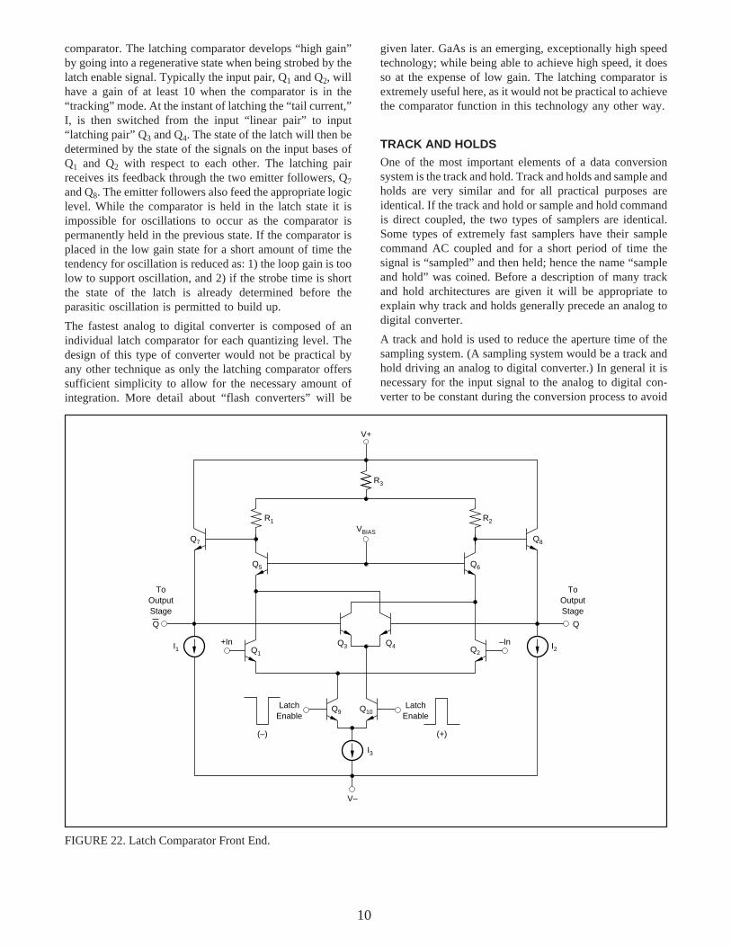
As previously mentioned, the other type of comparator thatis employed is known as the “latching type.” Figure 22shows a simplified schematic of the front end of this type of
VOUT
CS
Rg
VIN
82dB
70dB
0°
96°
180°
GT
100MHz
225MHzf
G = G1 X G2 X G3 X G4 = 7 X 7 X 7 X 35 = 12,000 → 82dB
Bω/STAGE = 225MHz
ØSHIFT = 4 X 45°C = 180°C
Loop GainOpenLoopGain
– InsertionGain
=
–70dB 20 log1
2π Rg f CS
–70dB 20 log1
2π (300)(225 X 106) X (0.1 X 10–12)
–70dB 27dB = 43dB
When = 0°, oscillation occurs.
A1 A2 A3 A4
f (Hz)
Pha
se (
°)
φ
φ
10
comparator. The latching comparator develops “high gain”by going into a regenerative state when being strobed by thelatch enable signal. Typically the input pair, Q1 and Q2, willhave a gain of at least 10 when the comparator is in the“tracking” mode. At the instant of latching the “tail current,”I, is then switched from the input “linear pair” to input“latching pair” Q3 and Q4. The state of the latch will then bedetermined by the state of the signals on the input bases ofQ1 and Q2 with respect to each other. The latching pairreceives its feedback through the two emitter followers, Q7
and Q8. The emitter followers also feed the appropriate logiclevel. While the comparator is held in the latch state it isimpossible for oscillations to occur as the comparator ispermanently held in the previous state. If the comparator isplaced in the low gain state for a short amount of time thetendency for oscillation is reduced as: 1) the loop gain is toolow to support oscillation, and 2) if the strobe time is shortthe state of the latch is already determined before theparasitic oscillation is permitted to build up.
The fastest analog to digital converter is composed of anindividual latch comparator for each quantizing level. Thedesign of this type of converter would not be practical byany other technique as only the latching comparator offerssufficient simplicity to allow for the necessary amount ofintegration. More detail about “flash converters” will be
given later. GaAs is an emerging, exceptionally high speedtechnology; while being able to achieve high speed, it doesso at the expense of low gain. The latching comparator isextremely useful here, as it would not be practical to achievethe comparator function in this technology any other way.
TRACK AND HOLDS
One of the most important elements of a data conversionsystem is the track and hold. Track and holds and sample andholds are very similar and for all practical purposes areidentical. If the track and hold or sample and hold commandis direct coupled, the two types of samplers are identical.Some types of extremely fast samplers have their samplecommand AC coupled and for a short period of time thesignal is “sampled” and then held; hence the name “sampleand hold” was coined. Before a description of many trackand hold architectures are given it will be appropriate toexplain why track and holds generally precede an analog todigital converter.
A track and hold is used to reduce the aperture time of thesampling system. (A sampling system would be a track andhold driving an analog to digital converter.) In general it isnecessary for the input signal to the analog to digital con-verter to be constant during the conversion process to avoid
I3
Q Q
–In+In
ToOutputStage
ToOutputStage
V+
V–
Q4Q3 Q2
Q6Q5
Q8Q7
LatchEnable
VBIAS
Q9 Q10
Q1
R3
R2R1
(+)
LatchEnable
(–)
I1 I2
FIGURE 22. Latch Comparator Front End.
11
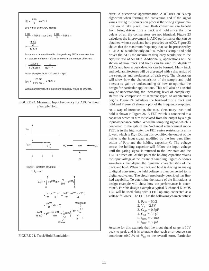
error. A successive approximation ADC uses an N-stepalgorithm when forming the conversion and if the signalvaries during the conversion process the wrong approxima-tion would take place. Even flash converters can benefitfrom being driven from a track and hold since the timedelays of all the comparators are not identical. Figure 23calculates the improvement in ADC performance that can beobtained when a track and hold precedes an ADC. Figure 23shows that the maximum frequency that can be processed bya 1µs ADC would be only 38.9Hz. When a sample and holddrives the ADC the maximum frequency would rise to theNyquist rate of 500kHz. Additionally, applications will beshown of how track and holds can be used to “deglitch”DACs and how a peak detector can be formed. Many trackand hold architectures will be presented with a discussion ofthe strengths and weaknesses of each type. The discussionwill show how the characteristics of the sample and holdinteract to gain an understanding of how to optimize thedesign for particular applications. This will also be a usefulway of understanding the increasing level of complexity.Before the comparison of different types of architecturesbegins, Figure 24 calculates the bandwidth of a track andhold and Figure 25 shows a plot of the frequency response.
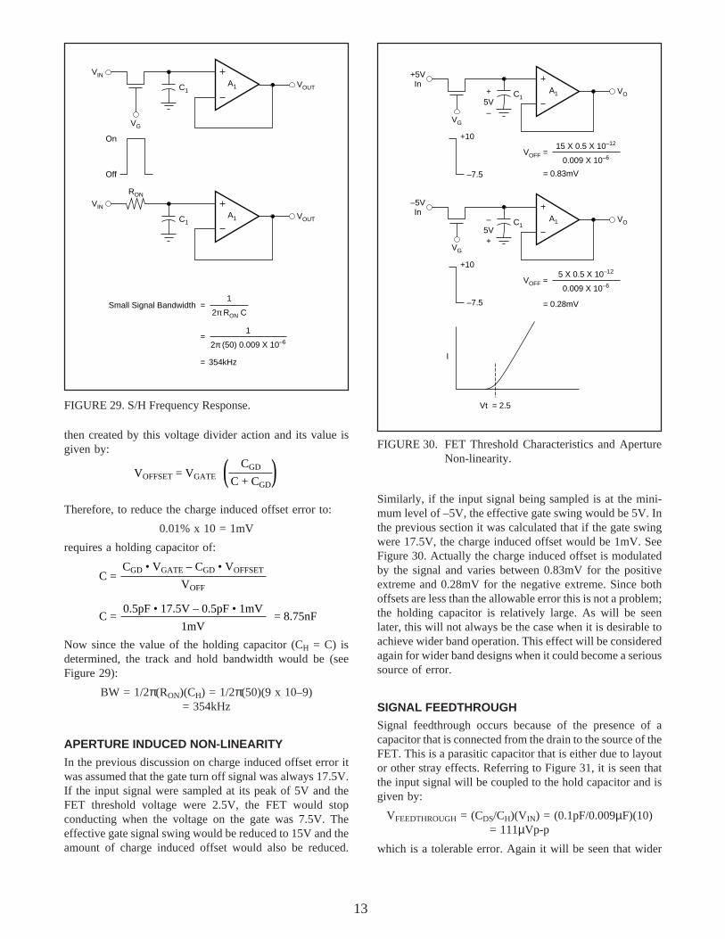
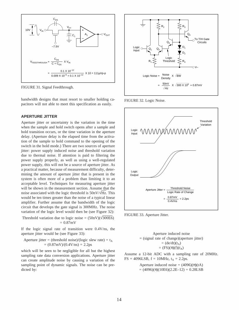
As a way of introduction, the most elementary track andhold is shown in Figure 26. A FET switch is connected to acapacitor which in turn is isolated from the output by a highinput-impedance buffer. When the sampling signal, which isconnected to the gate of the N-channel enhancement modeFET, is in the high state, the FET series resistance is at itslowest which is RON. During this condition the output of thebuffer is the input signal modified by the low pass filteraction of RON and the holding capacitor C. The voltageacross the holding capacitor will follow the input voltageuntil the gating signal is returned to the low state and theFET is turned off. At that point the holding capacitor retainsthe input voltage at the instant of sampling. Figure 27 showswaveforms that depict the dynamic characteristics of thetrack and hold. When the track and hold is driving an analogto digital converter, the held voltage is then converted to itsdigital equivalent. The circuit previously described has lim-ited capability. To determine the nature of the limitations, adesign example will show how the performance is deter-mined. For this design example a typical N-channel D-MOSFET will be used along with a FET op amp connected as avoltage follower. The FET has the following characteristics:
1. RON = 50Ω2. VT = 2.5V3. CGD = 0.5pF4. CDS = 0.1pF5. IDSS = 25mA6. IOFF = 50pA
Assume for this example that the input signal range is 10Vpeak to peak and it is tolerable that each error source cancontribute ±0.01% of VIN to the overall error. Particular
FIGURE 23. Maximum Input Frequency for ADC Withouta Sample/Hold.
e(t) =EFS
2
EFS = Full Scale ADC Range
sin 2π ft
= f EFS π cos 2π ft,d e(t)
dt= f EFS π
d e(t)dt
f =EFS π
d e(t)dt
Assume maximum allowable change during ADC conversion time.
T = 1/2LSB and EFS = 2NLSB where N is the number of bit ADC.
f =1/2LSB
T 2NLSB π=
1
π 2(N + 1) T
As an example, let N = 12 and T = 1µs:
fMAX =1/2LSB
T 2NLSB π= 38.9Hz
With a sample/hold, the maximum frequency would be 500kHz.
FIGURE 24. Track/Hold Bandwidth.
T/HeIN eOUT
fs
eIN
eOUT V
Fourier Transform of Output
tfS
EO(f) =
( )EO(f)
EO(o)
Vj2πf
o
T
Vej2πft dt = (ej2πft)
o
T
Vπf
=ej2πfT – 1
2jVejπfT
πf=
(ejπfT – e–jπfT)2j
=VejπfT
πfsin π fT
= ejπfT sin π fTπ fT
= ejπ(f/fs)sin π f
fsπffs
)(Magnitude
Phase
12
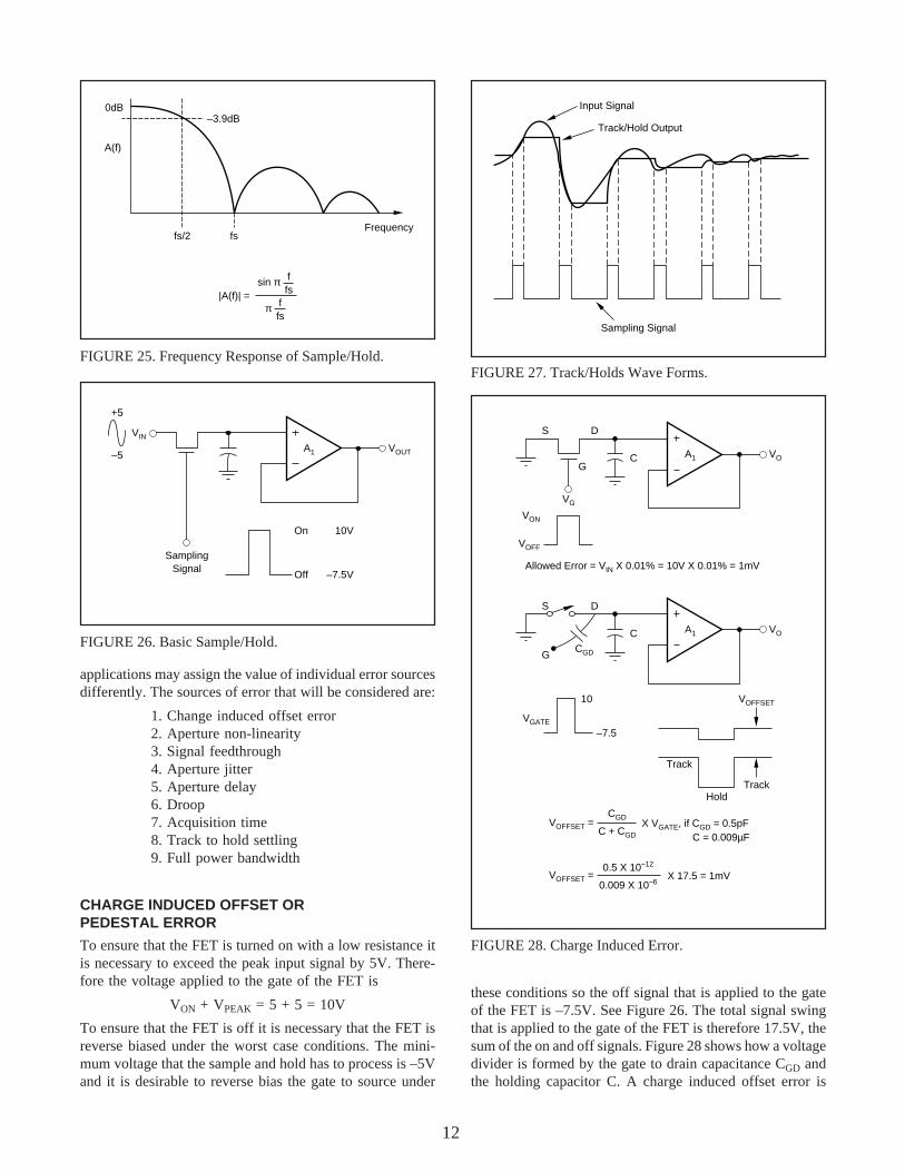
FIGURE 25. Frequency Response of Sample/Hold.
A(f)
0dB
Frequencyfs/2 fs
–3.9dB
|A(f)| =sin π f
fs
π ffs
SamplingSignal
VOUT
VIN
+5
–5
On
Off
10V
–7.5V
A1
FIGURE 26. Basic Sample/Hold.
FIGURE 27. Track/Holds Wave Forms.
Sampling Signal
Track/Hold Output
Input Signal
VO
DS
CG
VON
VOFF
VO
DS
C
G
VGATE
Allowed Error = VIN X 0.01% = 10V X 0.01% = 1mV
CGD
10
–7.5
VOFFSET
Track
Track
Hold
VOFFSET = X VGATE, if CGD = 0.5pFC = 0.009µF
VOFFSET = X 17.5 = 1mV
CGD
C + CGD
0.5 X 10⁻¹²
0.009 X 10⁻⁶
VG
A1
A1
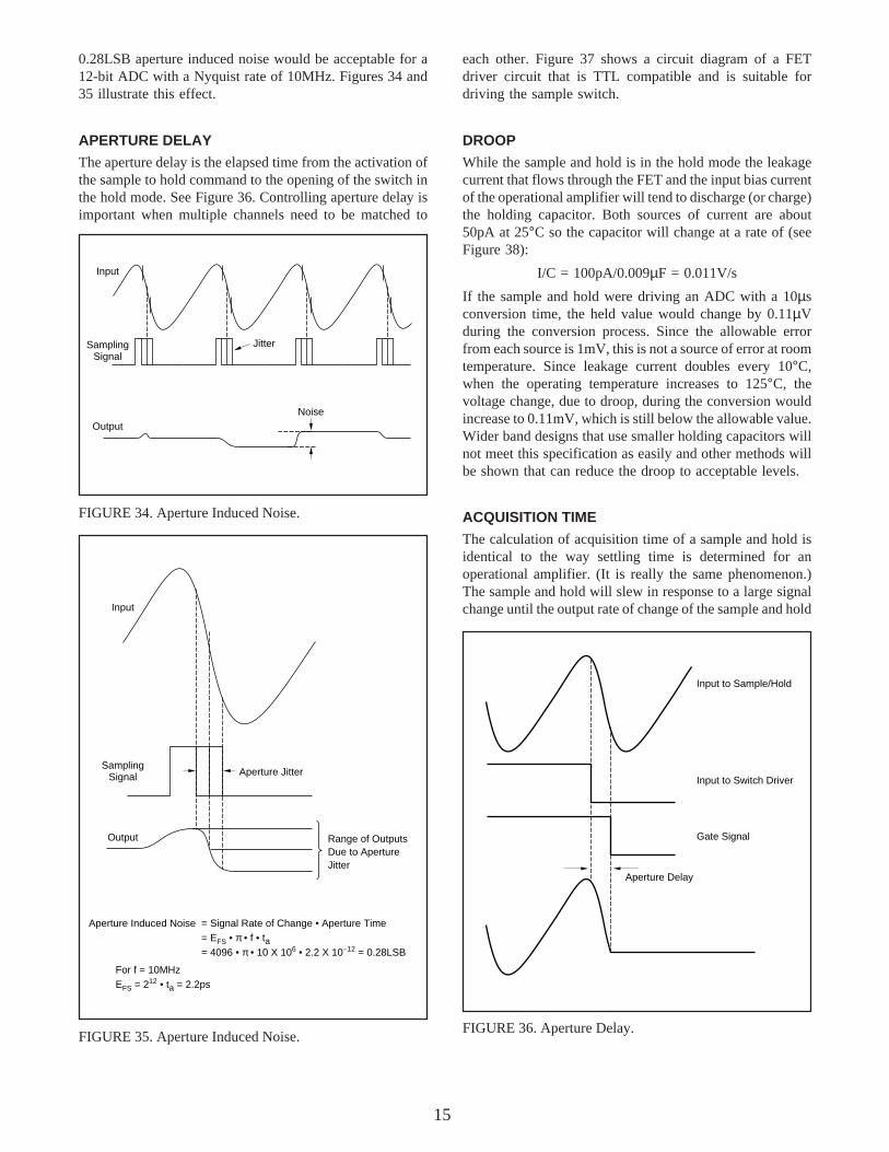
FIGURE 28. Charge Induced Error.
applications may assign the value of individual error sourcesdifferently. The sources of error that will be considered are:
1. Change induced offset error2. Aperture non-linearity3. Signal feedthrough4. Aperture jitter5. Aperture delay6. Droop7. Acquisition time8. Track to hold settling9. Full power bandwidth
CHARGE INDUCED OFFSET ORPEDESTAL ERROR
To ensure that the FET is turned on with a low resistance itis necessary to exceed the peak input signal by 5V. There-fore the voltage applied to the gate of the FET is
VON + VPEAK = 5 + 5 = 10V
To ensure that the FET is off it is necessary that the FET isreverse biased under the worst case conditions. The mini-mum voltage that the sample and hold has to process is –5Vand it is desirable to reverse bias the gate to source under
these conditions so the off signal that is applied to the gateof the FET is –7.5V. See Figure 26. The total signal swingthat is applied to the gate of the FET is therefore 17.5V, thesum of the on and off signals. Figure 28 shows how a voltagedivider is formed by the gate to drain capacitance CGD andthe holding capacitor C. A charge induced offset error is
13
then created by this voltage divider action and its value isgiven by:
VOFFSET = VGATE
CGD
C + CGD( )
Therefore, to reduce the charge induced offset error to:
0.01% x 10 = 1mV
requires a holding capacitor of:
C =CGD • VGATE – CGD • VOFFSET
VOFF
C =0.5pF • 17.5V – 0.5pF • 1mV
1mV= 8.75nF
Now since the value of the holding capacitor (CH = C) isdetermined, the track and hold bandwidth would be (seeFigure 29):
BW = 1/2π(RON)(CH) = 1/2π(50)(9 x 10–9)= 354kHz
APERTURE INDUCED NON-LINEARITY
In the previous discussion on charge induced offset error itwas assumed that the gate turn off signal was always 17.5V.If the input signal were sampled at its peak of 5V and theFET threshold voltage were 2.5V, the FET would stopconducting when the voltage on the gate was 7.5V. Theeffective gate signal swing would be reduced to 15V and theamount of charge induced offset would also be reduced.
FIGURE 29. S/H Frequency Response.
VOUT
VIN
On
Off
VOUT
VIN
C1
C1
RON
Small Signal Bandwidth =1
2π RON C
=1
2π (50) 0.009 X 10–6
= 354kHz
VG
A1
A1
FIGURE 30. FET Threshold Characteristics and ApertureNon-linearity.
VO
+5VIn
+10
VOFF =15 X 0.5 X 10–12
0.009 X 10⁻⁶
–7.5
+5V–
VO
–5VIn
+10
VOFF =5 X 0.5 X 10–12
0.009 X 10⁻⁶
–7.5
–5V+
= 0.83mV
= 0.28mV
Vt = 2.5
I
VG
VG
A1
A1
C1
C1
Similarly, if the input signal being sampled is at the mini-mum level of –5V, the effective gate swing would be 5V. Inthe previous section it was calculated that if the gate swingwere 17.5V, the charge induced offset would be 1mV. SeeFigure 30. Actually the charge induced offset is modulatedby the signal and varies between 0.83mV for the positiveextreme and 0.28mV for the negative extreme. Since bothoffsets are less than the allowable error this is not a problem;the holding capacitor is relatively large. As will be seenlater, this will not always be the case when it is desirable toachieve wider band operation. This effect will be consideredagain for wider band designs when it could become a serioussource of error.
SIGNAL FEEDTHROUGH
Signal feedthrough occurs because of the presence of acapacitor that is connected from the drain to the source of theFET. This is a parasitic capacitor that is either due to layoutor other stray effects. Referring to Figure 31, it is seen thatthe input signal will be coupled to the hold capacitor and isgiven by:
VFEEDTHROUGH = (CDS/CH)(VIN) = (0.1pF/0.009µF)(10)= 111µVp-p
which is a tolerable error. Again it will be seen that wider
14
bandwidth designs that must resort to smaller holding ca-pacitors will not able to meet this specification as easily.
APERTURE JITTER
Aperture jitter or uncertainty is the variation in the timewhen the sample and hold switch opens after a sample andhold transition occurs, or the time variation in the aperturedelay. (Aperture delay is the elapsed time from the activa-tion of the sample to hold command to the opening of theswitch in the hold mode.) There are two sources of aperturejitter: power supply induced noise and threshold variationdue to thermal noise. If attention is paid to filtering thepower supply properly, as well as using a well-regulatedpower supply, this will not be a source of aperture jitter. Asa practical matter, because of measurement difficulty, deter-mining the amount of aperture jitter that is present in thesystem is often more of a problem than limiting it to anacceptable level. Techniques for measuring aperture jitterwill be shown in the measurement section. Assume that thenoise associated with the logic threshold is 50nV/√Hz. Thiswould be ten times greater than the noise of a typical linearamplifier. Further assume that the bandwidth of the logiccircuit that develops the gate signal is 300MHz. The noisevariation of the logic level would then be (see Figure 32):
Threshold variation due to logic noise = (50nV)(√300E6)= 0.87mV
If the logic signal rate of transition were 0.4V/ns, theaperture jitter would be (see Figure 33):
Aperture jitter = (threshold noise)/(logic slew rate) = tA
= (0.87mV)/(0.4V/ns) = 2.2ps
which will be seen to be negligible for all but the highestsampling rate data conversion applications. Aperture jittercan create amplitude noise by causing a variation of thesampling point of dynamic signals. The noise can be pre-dicted by:
VFEEDTHROUGH =CDS
C + CDS
=
–7.5V
VOUT
VIN10VVFT
C1
CDS
X VIN
0.1 X 10⁻¹²
0.009 X 10⁻⁶ + 0.1 X 10–12X 10 = 111µVp-p
A1
FIGURE 31. Signal Feedthrough.
LogicThreshold
V–
To T/H GateCircuits
LogicInput
Logic Noise = NoiseDensity
X BW
= 50nV
HzX 300 X 106 = 0.87mV
Q4
R3R2
D1
D2
R4R1
Q1 Q2
Q3
FIGURE 32. Logic Noise.
Aperture induced noise= (signal rate of change)(aperture jitter)
= (de/dt)(tA)= (FS)(π)(f)(tA)
Assume a 12-bit ADC with a sampling rate of 20MHz.FS = 4096LSB, f = 10MHz, tA = 2.2ps.
Aperture induced noise = (4096)(π)(tA)= (4096)(π)(10E6)(2.2E–12) = 0.28LSB
Aperture Jitter = Threshold NoiseLogic Rate of Change
LogicInput
ThresholdVariation
LogicOutput
= 0.87mV0.4V/ns
= 2.2ps
FIGURE 33. Aperture Jitter.
15
Input
SamplingSignal
Output
Jitter
Noise
Input
SamplingSignal
Output
Aperture Jitter
Range of OutputsDue to ApertureJitter
= Signal Rate of Change • Aperture Time= EFS • π • f • ta= 4096 • π • 10 X 106 • 2.2 X 10–12 = 0.28LSB
Aperture Induced Noise
For f = 10MHzEFS = 212 • ta = 2.2ps
FIGURE 35. Aperture Induced Noise.
FIGURE 34. Aperture Induced Noise.
0.28LSB aperture induced noise would be acceptable for a12-bit ADC with a Nyquist rate of 10MHz. Figures 34 and35 illustrate this effect.
APERTURE DELAY
The aperture delay is the elapsed time from the activation ofthe sample to hold command to the opening of the switch inthe hold mode. See Figure 36. Controlling aperture delay isimportant when multiple channels need to be matched to
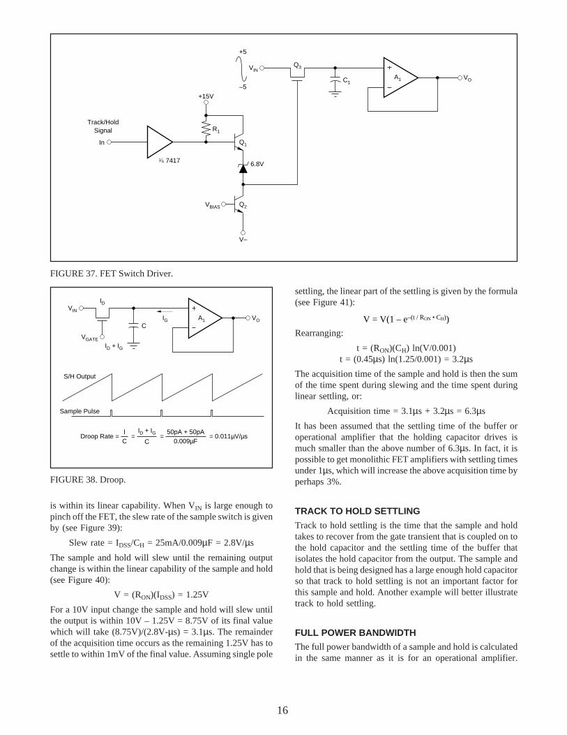
each other. Figure 37 shows a circuit diagram of a FETdriver circuit that is TTL compatible and is suitable fordriving the sample switch.
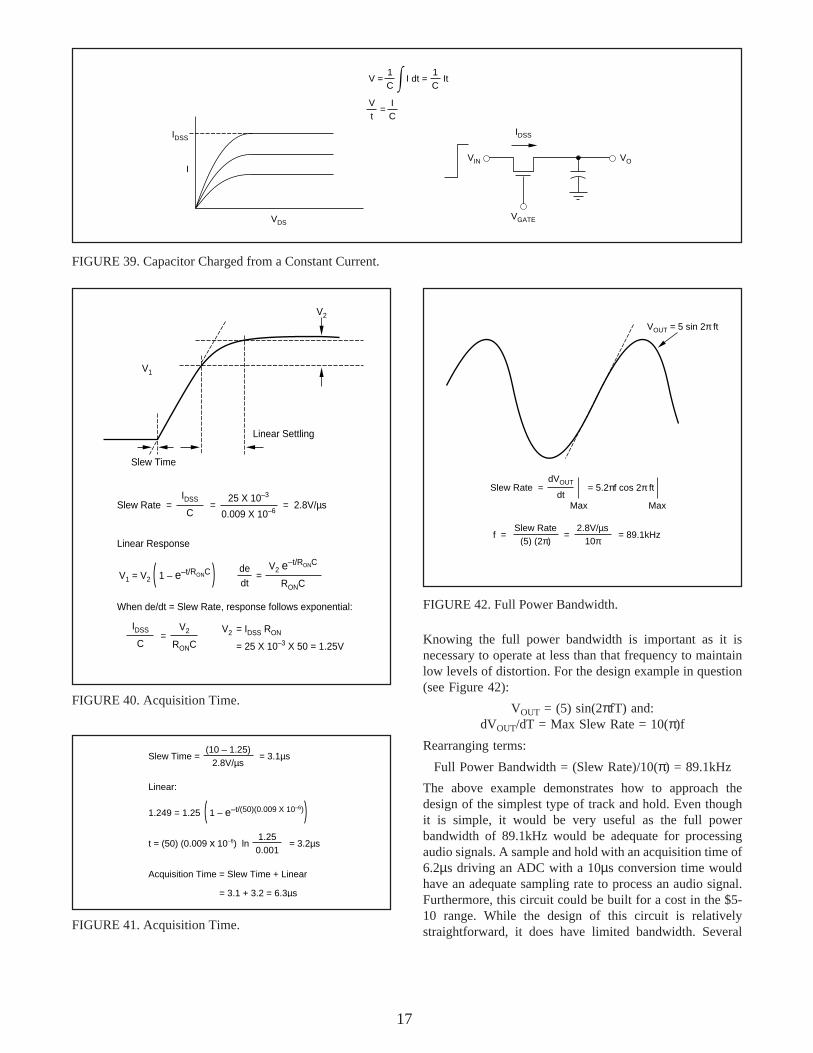
DROOP
While the sample and hold is in the hold mode the leakagecurrent that flows through the FET and the input bias currentof the operational amplifier will tend to discharge (or charge)the holding capacitor. Both sources of current are about50pA at 25°C so the capacitor will change at a rate of (seeFigure 38):
I/C = 100pA/0.009µF = 0.011V/s
If the sample and hold were driving an ADC with a 10µsconversion time, the held value would change by 0.11µVduring the conversion process. Since the allowable errorfrom each source is 1mV, this is not a source of error at roomtemperature. Since leakage current doubles every 10°C,when the operating temperature increases to 125°C, thevoltage change, due to droop, during the conversion wouldincrease to 0.11mV, which is still below the allowable value.Wider band designs that use smaller holding capacitors willnot meet this specification as easily and other methods willbe shown that can reduce the droop to acceptable levels.
ACQUISITION TIME
The calculation of acquisition time of a sample and hold isidentical to the way settling time is determined for anoperational amplifier. (It is really the same phenomenon.)The sample and hold will slew in response to a large signalchange until the output rate of change of the sample and hold
FIGURE 36. Aperture Delay.
Input to Sample/Hold
Input to Switch Driver
Gate Signal
Aperture Delay
16
VO
VIN
+5
–5
V–
+15V
6.8V
VBIAS
1 6 7417
Track/HoldSignal
In
A1C1
Q3
Q1
Q2
R1
is within its linear capability. When VIN is large enough topinch off the FET, the slew rate of the sample switch is givenby (see Figure 39):
Slew rate = IDSS/CH = 25mA/0.009µF = 2.8V/µs
The sample and hold will slew until the remaining outputchange is within the linear capability of the sample and hold(see Figure 40):
V = (RON)(IDSS) = 1.25V
For a 10V input change the sample and hold will slew untilthe output is within 10V – 1.25V = 8.75V of its final valuewhich will take (8.75V)/(2.8V-µs) = 3.1µs. The remainderof the acquisition time occurs as the remaining 1.25V has tosettle to within 1mV of the final value. Assuming single pole
FIGURE 37. FET Switch Driver.
VO
VIN
C
ID
ID + IG
IG
S/H Output
Sample Pulse
Droop Rate =IC
=ID + IG
C=
50pA + 50pA0.009µF
= 0.011µV/µs
A1
VGATE
FIGURE 38. Droop.
settling, the linear part of the settling is given by the formula(see Figure 41):
V = V(1 – e–(t / RON • CH))
Rearranging:
t = (RON)(CH) ln(V/0.001)t = (0.45µs) ln(1.25/0.001) = 3.2µs
The acquisition time of the sample and hold is then the sumof the time spent during slewing and the time spent duringlinear settling, or:
Acquisition time = 3.1µs + 3.2µs = 6.3µs
It has been assumed that the settling time of the buffer oroperational amplifier that the holding capacitor drives ismuch smaller than the above number of 6.3µs. In fact, it ispossible to get monolithic FET amplifiers with settling timesunder 1µs, which will increase the above acquisition time byperhaps 3%.
TRACK TO HOLD SETTLING
Track to hold settling is the time that the sample and holdtakes to recover from the gate transient that is coupled on tothe hold capacitor and the settling time of the buffer thatisolates the hold capacitor from the output. The sample andhold that is being designed has a large enough hold capacitorso that track to hold settling is not an important factor forthis sample and hold. Another example will better illustratetrack to hold settling.
FULL POWER BANDWIDTH
The full power bandwidth of a sample and hold is calculatedin the same manner as it is for an operational amplifier.
17
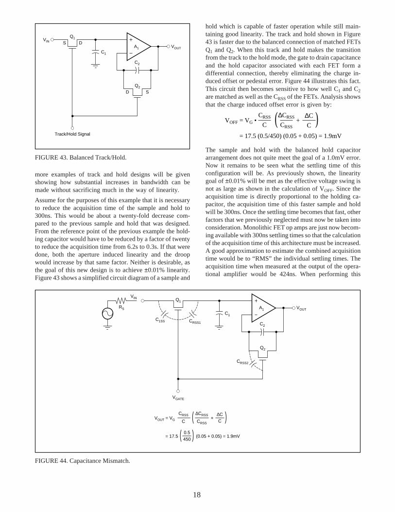
FIGURE 39. Capacitor Charged from a Constant Current.
VIN VO
IDSS
VDS
I
IDSS
V = I dt =1C
It1C
IC
=Vt
VGATE
Slew Rate =dVOUT
dt
VOUT = 5 sin 2π ft
= 5.2πf cos 2π ft
Max Max
f =Slew Rate
(5) (2π)= 89.1kHz=
2.8V/µs10π
FIGURE 42. Full Power Bandwidth.
Slew Time =(10 – 1.25)
2.8V/µs
1.249 = 1.25
Linear:
= 3.1µs
1 – e–t/(50)(0.009 X 10–6)( )t = (50) (0.009 x 10⁻⁶) ln
1.250.001
= 3.2µs
Acquisition Time = Slew Time + Linear
= 3.1 + 3.2 = 6.3µs
FIGURE 41. Acquisition Time.
Knowing the full power bandwidth is important as it isnecessary to operate at less than that frequency to maintainlow levels of distortion. For the design example in question(see Figure 42):
VOUT = (5) sin(2πfT) and:dVOUT/dT = Max Slew Rate = 10(π)f
Rearranging terms:
Full Power Bandwidth = (Slew Rate)/10(π) = 89.1kHz
The above example demonstrates how to approach thedesign of the simplest type of track and hold. Even thoughit is simple, it would be very useful as the full powerbandwidth of 89.1kHz would be adequate for processingaudio signals. A sample and hold with an acquisition time of6.2µs driving an ADC with a 10µs conversion time wouldhave an adequate sampling rate to process an audio signal.Furthermore, this circuit could be built for a cost in the $5-10 range. While the design of this circuit is relativelystraightforward, it does have limited bandwidth. Several
FIGURE 40. Acquisition Time.
Slew Rate =
V1 = V2 ( )
IDSS
C
Linear Settling
V2
V1
1 – e–t/RONC
25 X 10–3
0.009 X 10–6= = 2.8V/µs
Linear Response
=dedt
V2 e–t/RONC
RONC
When de/dt = Slew Rate, response follows exponential:
IDSS
C=
V2
RONC
= IDSS RON
= 25 X 10–3 X 50 = 1.25V
V2
Slew Time
18
more examples of track and hold designs will be givenshowing how substantial increases in bandwidth can bemade without sacrificing much in the way of linearity.
Assume for the purposes of this example that it is necessaryto reduce the acquisition time of the sample and hold to300ns. This would be about a twenty-fold decrease com-pared to the previous sample and hold that was designed.From the reference point of the previous example the hold-ing capacitor would have to be reduced by a factor of twentyto reduce the acquisition time from 6.2s to 0.3s. If that weredone, both the aperture induced linearity and the droopwould increase by that same factor. Neither is desirable, asthe goal of this new design is to achieve ±0.01% linearity.Figure 43 shows a simplified circuit diagram of a sample and
hold which is capable of faster operation while still main-taining good linearity. The track and hold shown in Figure43 is faster due to the balanced connection of matched FETsQ1 and Q2. When this track and hold makes the transitionfrom the track to the hold mode, the gate to drain capacitanceand the hold capacitor associated with each FET form adifferential connection, thereby eliminating the charge in-duced offset or pedestal error. Figure 44 illustrates this fact.This circuit then becomes sensitive to how well C1 and C2
are matched as well as the CRSS of the FETs. Analysis showsthat the charge induced offset error is given by:
VOFF = VG •CRSS
C
∆CRSS
CRSS
∆C
C+
= 17.5 (0.5/450) (0.05 + 0.05) = 1.9mV
( )
The sample and hold with the balanced hold capacitorarrangement does not quite meet the goal of a 1.0mV error.Now it remains to be seen what the settling time of thisconfiguration will be. As previously shown, the linearitygoal of ±0.01% will be met as the effective voltage swing isnot as large as shown in the calculation of VOFF. Since theacquisition time is directly proportional to the holding ca-pacitor, the acquisition time of this faster sample and holdwill be 300ns. Once the settling time becomes that fast, otherfactors that we previously neglected must now be taken intoconsideration. Monolithic FET op amps are just now becom-ing available with 300ns settling times so that the calculationof the acquisition time of this architecture must be increased.A good approximation to estimate the combined acquisitiontime would be to “RMS” the individual settling times. Theacquisition time when measured at the output of the opera-tional amplifier would be 424ns. When performing this
FIGURE 43. Balanced Track/Hold.
VOUT
VIN
C1
Q1
Q2
C2
DS
Track/Hold Signal
D S
A1
FIGURE 44. Capacitance Mismatch.
VOUT
VIN
C1
Q2
C2
VGATE
CRSS1
CRSS2
C1SS
RS
VOUT = VG
CRSS
C ( )∆CRSS
CRSS+
∆CC
( )0.5450
= 17.5 (0.05 + 0.05) = 1.9mV
A1
Q1
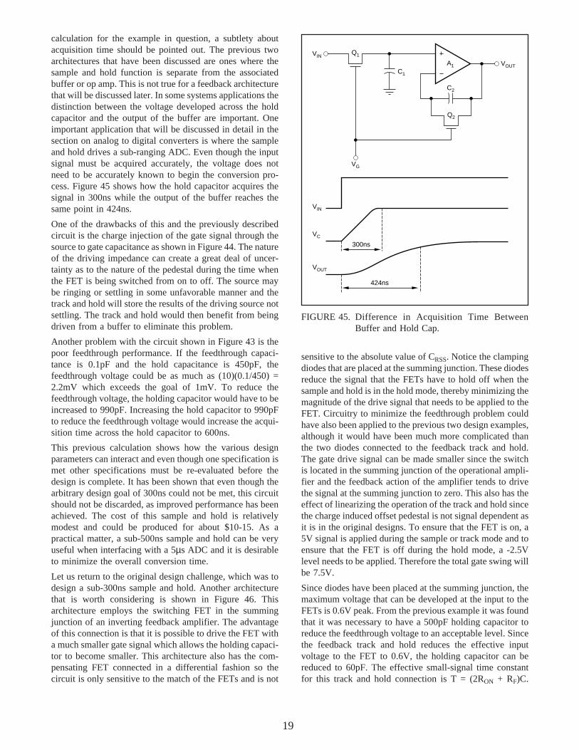
19
calculation for the example in question, a subtlety aboutacquisition time should be pointed out. The previous twoarchitectures that have been discussed are ones where thesample and hold function is separate from the associatedbuffer or op amp. This is not true for a feedback architecturethat will be discussed later. In some systems applications thedistinction between the voltage developed across the holdcapacitor and the output of the buffer are important. Oneimportant application that will be discussed in detail in thesection on analog to digital converters is where the sampleand hold drives a sub-ranging ADC. Even though the inputsignal must be acquired accurately, the voltage does notneed to be accurately known to begin the conversion pro-cess. Figure 45 shows how the hold capacitor acquires thesignal in 300ns while the output of the buffer reaches thesame point in 424ns.
One of the drawbacks of this and the previously describedcircuit is the charge injection of the gate signal through thesource to gate capacitance as shown in Figure 44. The natureof the driving impedance can create a great deal of uncer-tainty as to the nature of the pedestal during the time whenthe FET is being switched from on to off. The source maybe ringing or settling in some unfavorable manner and thetrack and hold will store the results of the driving source notsettling. The track and hold would then benefit from beingdriven from a buffer to eliminate this problem.
Another problem with the circuit shown in Figure 43 is thepoor feedthrough performance. If the feedthrough capaci-tance is 0.1pF and the hold capacitance is 450pF, thefeedthrough voltage could be as much as (10)(0.1/450) =2.2mV which exceeds the goal of 1mV. To reduce thefeedthrough voltage, the holding capacitor would have to beincreased to 990pF. Increasing the hold capacitor to 990pFto reduce the feedthrough voltage would increase the acqui-sition time across the hold capacitor to 600ns.
This previous calculation shows how the various designparameters can interact and even though one specification ismet other specifications must be re-evaluated before thedesign is complete. It has been shown that even though thearbitrary design goal of 300ns could not be met, this circuitshould not be discarded, as improved performance has beenachieved. The cost of this sample and hold is relativelymodest and could be produced for about $10-15. As apractical matter, a sub-500ns sample and hold can be veryuseful when interfacing with a 5µs ADC and it is desirableto minimize the overall conversion time.
Let us return to the original design challenge, which was todesign a sub-300ns sample and hold. Another architecturethat is worth considering is shown in Figure 46. Thisarchitecture employs the switching FET in the summingjunction of an inverting feedback amplifier. The advantageof this connection is that it is possible to drive the FET witha much smaller gate signal which allows the holding capaci-tor to become smaller. This architecture also has the com-pensating FET connected in a differential fashion so thecircuit is only sensitive to the match of the FETs and is not
sensitive to the absolute value of CRSS. Notice the clampingdiodes that are placed at the summing junction. These diodesreduce the signal that the FETs have to hold off when thesample and hold is in the hold mode, thereby minimizing themagnitude of the drive signal that needs to be applied to theFET. Circuitry to minimize the feedthrough problem couldhave also been applied to the previous two design examples,although it would have been much more complicated thanthe two diodes connected to the feedback track and hold.The gate drive signal can be made smaller since the switchis located in the summing junction of the operational ampli-fier and the feedback action of the amplifier tends to drivethe signal at the summing junction to zero. This also has theeffect of linearizing the operation of the track and hold sincethe charge induced offset pedestal is not signal dependent asit is in the original designs. To ensure that the FET is on, a5V signal is applied during the sample or track mode and toensure that the FET is off during the hold mode, a -2.5Vlevel needs to be applied. Therefore the total gate swing willbe 7.5V.
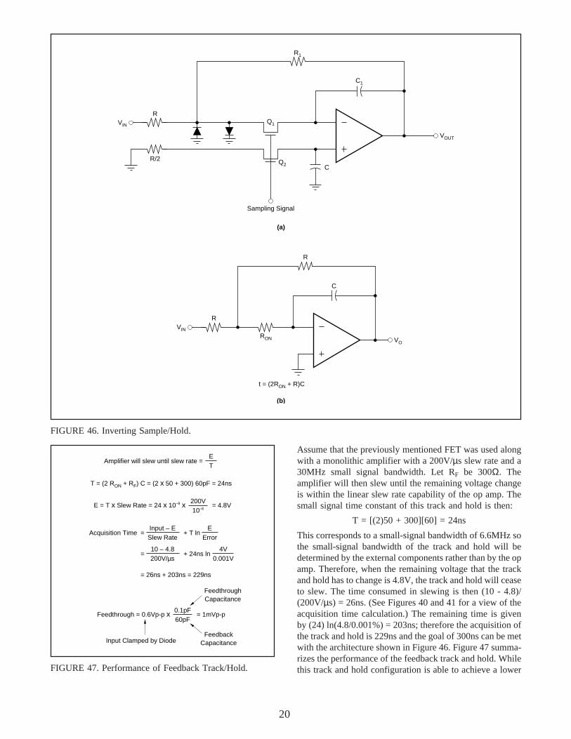
Since diodes have been placed at the summing junction, themaximum voltage that can be developed at the input to theFETs is 0.6V peak. From the previous example it was foundthat it was necessary to have a 500pF holding capacitor toreduce the feedthrough voltage to an acceptable level. Sincethe feedback track and hold reduces the effective inputvoltage to the FET to 0.6V, the holding capacitor can bereduced to 60pF. The effective small-signal time constantfor this track and hold connection is T = (2RON + RF)C.
VOUT
VIN
VIN
VC
VOUT
300ns
424ns
VG
Q1
C1
C2
Q2
A1
FIGURE 45. Difference in Acquisition Time BetweenBuffer and Hold Cap.
20
Assume that the previously mentioned FET was used alongwith a monolithic amplifier with a 200V/µs slew rate and a30MHz small signal bandwidth. Let RF be 300Ω. Theamplifier will then slew until the remaining voltage changeis within the linear slew rate capability of the op amp. Thesmall signal time constant of this track and hold is then:
T = [(2)50 + 300][60] = 24ns
This corresponds to a small-signal bandwidth of 6.6MHz sothe small-signal bandwidth of the track and hold will bedetermined by the external components rather than by the opamp. Therefore, when the remaining voltage that the trackand hold has to change is 4.8V, the track and hold will ceaseto slew. The time consumed in slewing is then (10 - 4.8)/(200V/µs) = 26ns. (See Figures 40 and 41 for a view of theacquisition time calculation.) The remaining time is givenby (24) ln(4.8/0.001%) = 203ns; therefore the acquisition ofthe track and hold is 229ns and the goal of 300ns can be metwith the architecture shown in Figure 46. Figure 47 summa-rizes the performance of the feedback track and hold. Whilethis track and hold configuration is able to achieve a lower
VOUT
VIN
C
R
R/2
R1
C1
Sampling Signal
(a)
VO
VIN
R
R
C
RON
t = (2RON + R)C
(b)
Q1
Q2
FIGURE 47. Performance of Feedback Track/Hold.
FIGURE 46. Inverting Sample/Hold.
Amplifier will slew until slew rate =ET
T = (2 RON + RF) C = (2 x 50 + 300) 60pF = 24ns
E = T x Slew Rate = 24 x 10–9 x 200V10–6
= 4.8V
Acquisition Time =Input – ESlew Rate
+ T lnE
Error
=10 – 4.8200V/µs
+ 24ns ln4V
0.001V
= 26ns + 203ns = 229ns
Feedthrough = 0.6Vp-p x 0.1pF60pF
= 1mVp-p
FeedthroughCapacitance
FeedbackCapacitanceInput Clamped by Diode

21
VOUT
VIN
CR1
CR3 CR4
CR2
C
Q1 Q2
Q3 Q4
I
I
V–
V+
HighSpeed
Op Amp
R1
R2
BufferA1
acquisition time, it does so at the expense of a lower inputimpedance. This may not be much of a penalty as the inputimpedance of 300Ω is within the capability of many op ampsto drive with ±5V input.
The last track and hold that will be described is capable ofacquisition times that are about an order of magnitude fasterthan the last one that was described. This track and hold,shown in Figure 48, shares some of the architectural featuresof the previously described ones, although the samplingelement is different. This higher speed sample and hold useshot carrier diodes in a bridge configuration to form thesampling element. Diodes, while more complex to form asample and hold, achieve high sampling speed due to thelower time constant compared to a FET and lower thresholdvoltages. As an example, a hot carrier diode operated at 5mAhas a resistance of 5Ω, VD of 0.6V and a capacitance of 5pF.Figure 48 shows a diagram of a sample and hold that has anacquisition time of 40ns to ±0.02% for a 2V step input. Thissample and hold has a measured aperture time of under 3ps.(A technique to measure aperture time is shown in themeasurement section.) The sampling function is performedby switching the bridge of hot carrier diodes CR1 through
CR4 from the “on” to the “off” state. During the samplemode the current I is steered through the diode bridge byturning on transistors Q2 through Q4. The bridge is returnedto the hold mode by turning Q3 and Q4 off and turning Q1and Q3 on. The action of turning Q1 and Q3 on creates anegative bias on CR1 and CR4. Since these bias voltages arereferenced to the output, creating “bootstrap effect,” thereverse bias voltage that diodes CR1 through CR4 experiencebecomes independent of signal level. This is an importantaspect of the design as this action prevents the charge offsetpedestal from becoming a non-linear function of signallevel. An ECL signal is coupled to switching transistors Q1
through Q4. The hold capacitor is isolated from the output bythe type of high speed buffers and op amps described in theamplifier section. The sampling bridge is isolated from theanalog input signal by a high speed open loop buffer.
As a means of comparison, calculations will demonstrate thedifferent performance parameters of this track and hold. Aswill be seen from the calculations below, the diode bridgewill not achieve as accurate performance as compared to theFET designs.
FIGURE 48. Very High Speed Sample/Hold.
22
CHARGE INDUCED PEDESTAL ERROR
To ensure that the diode bridge is always off, the diodebridge is driven by a complementary signal at the top andbottom of the bridge. The charge induced pedestal error isprincipally due to the diode capacitance mismatch and isdriven by (see Figure 49):
VOFF = (VOFF)(CD1 – CD2)/C
With care diodes can be matched to 0.025pF. (In actualpractice means are provided to adjust the capacitance to thislevel and once the adjustment is performed the difference indiode capacitance can be held to 0.025pF.) For properdynamic operation VG = 2V and the holding capacitor is40pF. Substituting into the above equation yields:
VOFF = (2)(0.025/40) = 1.3mV
Unlike the FET designs, this is strictly an offset error as thebootstrapping action renders this offset voltage independentof signal level.
SWITCH DELAY PEDESTAL ERROR
The diode bridge switching arrangement has an additionalsource of error that is not possessed by the FET switch. If thecurrent sources that bias the bridge are not symmetricallyswitched, the hold capacitor will start to discharge until theother current source is switched. This error manifests itselfat the system level as if it were an offset voltage. To a firstapproximation the cross-coupling eliminates the time mis-matching that exists between the NPN and PNP switchingpairs. However, due to second order effects as a result ofdifferent levels of parasitic capacitances, there is typically as
much as a 50ps mismatch between the complementarysignals that switch the bridge. This translates to an offsetvoltage of (see Figure 50, assume a bridge current of 1 or5mA):
VOFF = I(T/C) = 5mA (50ps/40pF) = 6.3mV
This effect is also largely independent of signal level due tothe bootstrapping.
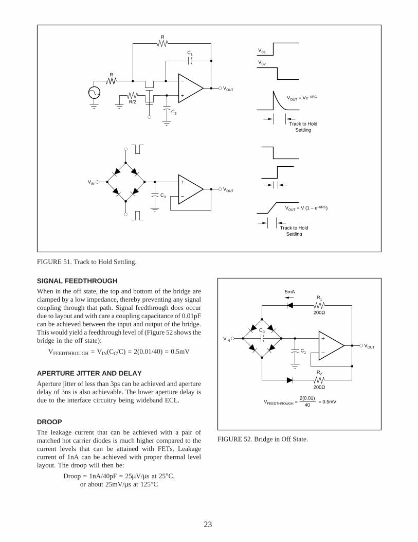
TRACK TO HOLD SETTLING
Track to hold settling is a measure of the recovery time ofthe track and hold in response to the track and hold goinginto the hold mode. The previous three architectures aredependent upon the sampling element, whether it is a FETor a diode, to switch exactly with identical waveform shapeand turn-off characteristics. In general this will not happenand a small signal will be injected into the buffer op amp.Track to hold settling is a complex calculation and represen-tative waveshapes are shown in Figure 51.
FIGURE 49. Pedestal for Diode Bridge.
VOFF
V+
C1
V–
VOFF =I x T
C
VIN
I1
I2
VG1
VG2
VG1 VG2
T
=5 x 10–3 x 50 x 10–12
40 x 10–12
= 6.3mV
Q1 Q2
Q3 Q4
FIGURE 50. Switch Delay.
VOFF
CD1
V+
C1
V–
CD2
VG
VG
VOFF = VG X(CD1 – CD2)
C=
2(0.025)40
= 1.3mV
VIN
I1
I2
23
SIGNAL FEEDTHROUGH
When in the off state, the top and bottom of the bridge areclamped by a low impedance, thereby preventing any signalcoupling through that path. Signal feedthrough does occurdue to layout and with care a coupling capacitance of 0.01pFcan be achieved between the input and output of the bridge.This would yield a feedthrough level of (Figure 52 shows thebridge in the off state):
VFEEDTHROUGH = VIN(CC/C) = 2(0.01/40) = 0.5mV
APERTURE JITTER AND DELAY
Aperture jitter of less than 3ps can be achieved and aperturedelay of 3ns is also achievable. The lower aperture delay isdue to the interface circuitry being wideband ECL.
DROOP
The leakage current that can be achieved with a pair ofmatched hot carrier diodes is much higher compared to thecurrent levels that can be attained with FETs. Leakagecurrent of 1nA can be achieved with proper thermal levellayout. The droop will then be:
Droop = 1nA/40pF = 25µV/µs at 25°C,or about 25mV/µs at 125°C
VC1
VOUT
R
VOUT
R
C1
C2
Track to HoldSettling
VC2
VOUT = Ve–t/RC
Track to HoldSettling
VOUT = V (1 – e–t/RC)
R/2
C3
VIN
FIGURE 51. Track to Hold Settling.
VOUT
CC
VIN
5mAR1
200Ω
C1
VFEEDTHROUGH = = 0.5mV2(0.01)
40
R2
200Ω
FIGURE 52. Bridge in Off State.
24
ACQUISITION TIMEAND FULL POWER BANDWIDTH
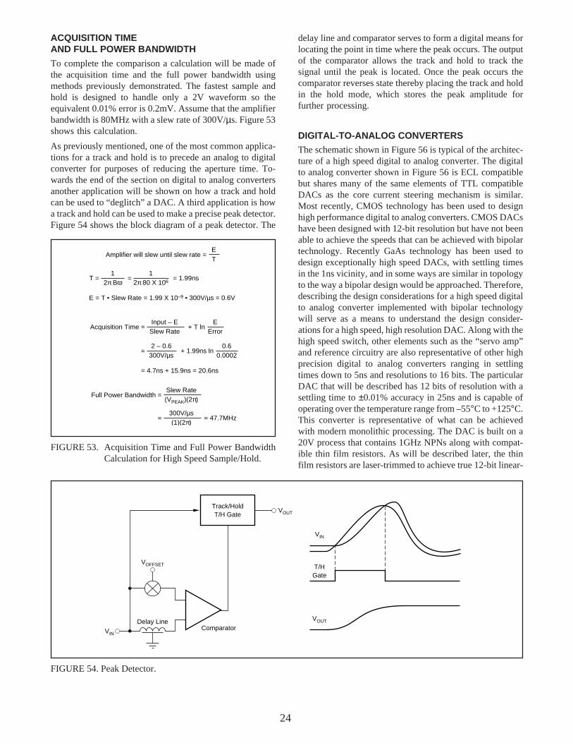
To complete the comparison a calculation will be made ofthe acquisition time and the full power bandwidth usingmethods previously demonstrated. The fastest sample andhold is designed to handle only a 2V waveform so theequivalent 0.01% error is 0.2mV. Assume that the amplifierbandwidth is 80MHz with a slew rate of 300V/µs. Figure 53shows this calculation.
As previously mentioned, one of the most common applica-tions for a track and hold is to precede an analog to digitalconverter for purposes of reducing the aperture time. To-wards the end of the section on digital to analog convertersanother application will be shown on how a track and holdcan be used to “deglitch” a DAC. A third application is howa track and hold can be used to make a precise peak detector.Figure 54 shows the block diagram of a peak detector. The
delay line and comparator serves to form a digital means forlocating the point in time where the peak occurs. The outputof the comparator allows the track and hold to track thesignal until the peak is located. Once the peak occurs thecomparator reverses state thereby placing the track and holdin the hold mode, which stores the peak amplitude forfurther processing.
DIGITAL-TO-ANALOG CONVERTERS
The schematic shown in Figure 56 is typical of the architec-ture of a high speed digital to analog converter. The digitalto analog converter shown in Figure 56 is ECL compatiblebut shares many of the same elements of TTL compatibleDACs as the core current steering mechanism is similar.Most recently, CMOS technology has been used to designhigh performance digital to analog converters. CMOS DACshave been designed with 12-bit resolution but have not beenable to achieve the speeds that can be achieved with bipolartechnology. Recently GaAs technology has been used todesign exceptionally high speed DACs, with settling timesin the 1ns vicinity, and in some ways are similar in topologyto the way a bipolar design would be approached. Therefore,describing the design considerations for a high speed digitalto analog converter implemented with bipolar technologywill serve as a means to understand the design consider-ations for a high speed, high resolution DAC. Along with thehigh speed switch, other elements such as the “servo amp”and reference circuitry are also representative of other highprecision digital to analog converters ranging in settlingtimes down to 5ns and resolutions to 16 bits. The particularDAC that will be described has 12 bits of resolution with asettling time to ±0.01% accuracy in 25ns and is capable ofoperating over the temperature range from –55°C to +125°C.This converter is representative of what can be achievedwith modern monolithic processing. The DAC is built on a20V process that contains 1GHz NPNs along with compat-ible thin film resistors. As will be described later, the thinfilm resistors are laser-trimmed to achieve true 12-bit linear-
FIGURE 54. Peak Detector.
Comparator
VOUT
VIN
Track/HoldT/H Gate
VOFFSET
VOUT
T/HGate
VIN
Delay Line
= = 1.99ns1
2π 80 X 106
Amplifier will slew until slew rate =ET
T =1
2π Bω
E = T • Slew Rate = 1.99 X 10⁻⁹ • 300V/µs = 0.6V
+ T lnE
ErrorAcquisition Time =
Input – ESlew Rate
+ 1.99ns ln0.6
0.0002=
2 – 0.6300V/µs
= 4.7ns + 15.9ns = 20.6ns
Full Power Bandwidth =Slew Rate(VPEAK)(2π)
=300V/µs(1)(2π)
= 47.7MHz
FIGURE 53. Acquisition Time and Full Power BandwidthCalculation for High Speed Sample/Hold.
25
ity over a very wide temperature range. Furthermore, thethin film resistors are capable of maintaining their accuracyover long periods of time and represent a reliable techniquefor producing a high speed, high resolution, low cost digitalto analog converter. The converter that will be described isentirely monolithic as it contains the precision currentswitches, servo amp, and low drift references. Only a fewcapacitors that are too large to be integrated and are neededfor filtering and bypassing are left off of the chip.
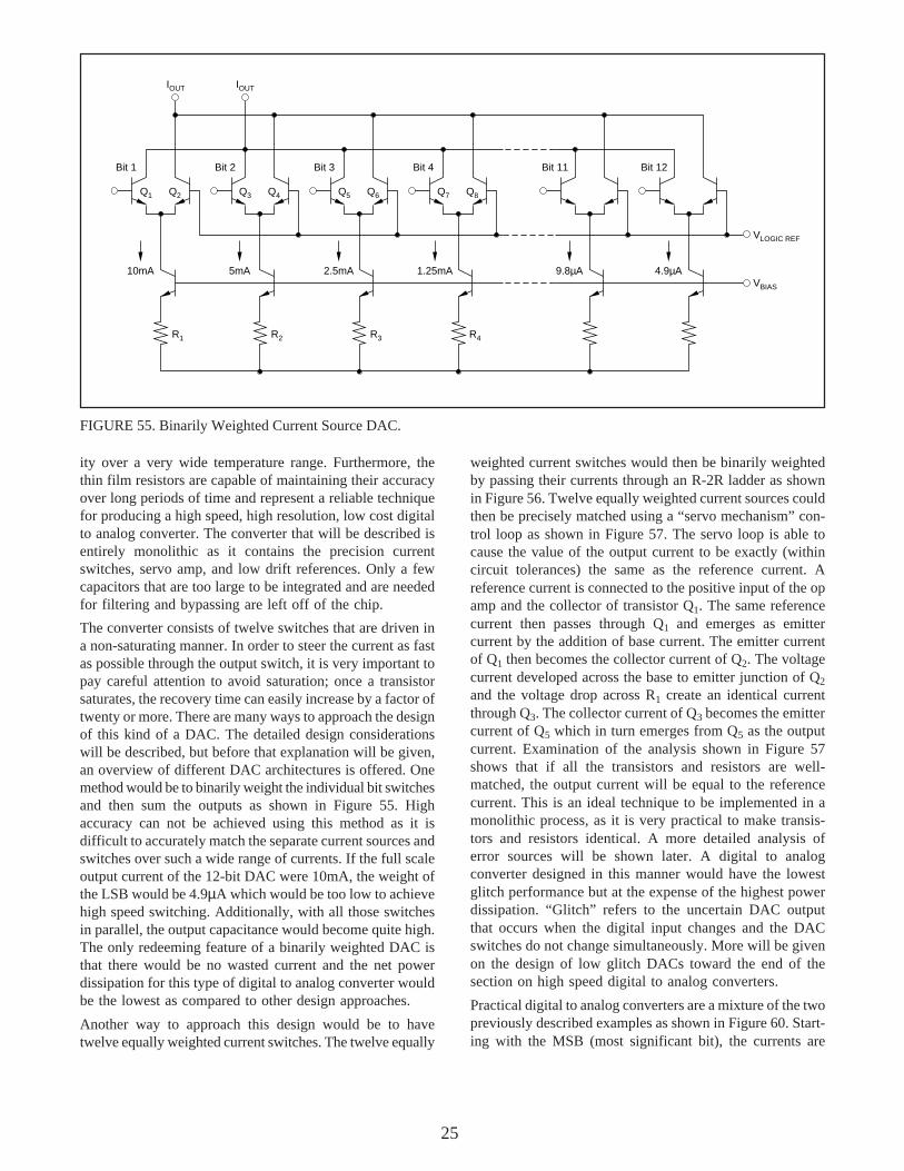
The converter consists of twelve switches that are driven ina non-saturating manner. In order to steer the current as fastas possible through the output switch, it is very important topay careful attention to avoid saturation; once a transistorsaturates, the recovery time can easily increase by a factor oftwenty or more. There are many ways to approach the designof this kind of a DAC. The detailed design considerationswill be described, but before that explanation will be given,an overview of different DAC architectures is offered. Onemethod would be to binarily weight the individual bit switchesand then sum the outputs as shown in Figure 55. Highaccuracy can not be achieved using this method as it isdifficult to accurately match the separate current sources andswitches over such a wide range of currents. If the full scaleoutput current of the 12-bit DAC were 10mA, the weight ofthe LSB would be 4.9µA which would be too low to achievehigh speed switching. Additionally, with all those switchesin parallel, the output capacitance would become quite high.The only redeeming feature of a binarily weighted DAC isthat there would be no wasted current and the net powerdissipation for this type of digital to analog converter wouldbe the lowest as compared to other design approaches.
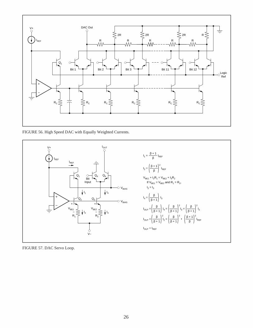
Another way to approach this design would be to havetwelve equally weighted current switches. The twelve equally
weighted current switches would then be binarily weightedby passing their currents through an R-2R ladder as shownin Figure 56. Twelve equally weighted current sources couldthen be precisely matched using a “servo mechanism” con-trol loop as shown in Figure 57. The servo loop is able tocause the value of the output current to be exactly (withincircuit tolerances) the same as the reference current. Areference current is connected to the positive input of the opamp and the collector of transistor Q1. The same referencecurrent then passes through Q1 and emerges as emittercurrent by the addition of base current. The emitter currentof Q1 then becomes the collector current of Q2. The voltagecurrent developed across the base to emitter junction of Q2
and the voltage drop across R1 create an identical currentthrough Q3. The collector current of Q3 becomes the emittercurrent of Q5 which in turn emerges from Q5 as the outputcurrent. Examination of the analysis shown in Figure 57shows that if all the transistors and resistors are well-matched, the output current will be equal to the referencecurrent. This is an ideal technique to be implemented in amonolithic process, as it is very practical to make transis-tors and resistors identical. A more detailed analysis oferror sources will be shown later. A digital to analogconverter designed in this manner would have the lowestglitch performance but at the expense of the highest powerdissipation. “Glitch” refers to the uncertain DAC outputthat occurs when the digital input changes and the DACswitches do not change simultaneously. More will be givenon the design of low glitch DACs toward the end of thesection on high speed digital to analog converters.
Practical digital to analog converters are a mixture of the twopreviously described examples as shown in Figure 60. Start-ing with the MSB (most significant bit), the currents are
FIGURE 55. Binarily Weighted Current Source DAC.
10mA
Bit 1
5mA
Bit 2
2.5mA
Bit 3
1.25mA
Bit 4
9.8µA
Bit 11
4.9µA
Bit 12
VBIAS
IOUT IOUT
Q1 Q2 Q3 Q4 Q5 Q6 Q7 Q8
R1 R2 R3 R4
VLOGIC REF
26
Bit 1 Bit 2 Bit 3 Bit 11 Bit 12LogicRef
DAC Out
RC RCRCRCRCRC
R
V+
IREF R R R R
2R 2R 2R R
Q1
FIGURE 56. High Speed DAC with Equally Weighted Currents.
BitInput
IOUT
R1
V+
IREF
VBIAS
VBIAS
V–
R2
VBE1 VBE2
+
–
+
– I2 I3
I1 I4
IREF
Q1
Q2 Q3
Q4 Q5
I1 =β + 1
βIREF
I2 =β + 1
βIREF( ) 2
VBE1 + I2R1 = VBE2 + I3R2
If VBE1 = VBE2 and R1 = R2,
I2 = I3
I4 =β
β + 1I3( )
IOUT =β
β + 1( ) I4 =β
β + 1( ) 2
I3 =β
β + 1( ) 2
I2
IOUT =β
β + 1( ) I2 =β
β + 1( ) 2
•β + 1
β( ) 2
IREF
2
IOUT = IREF
FIGURE 57. DAC Servo Loop.
27
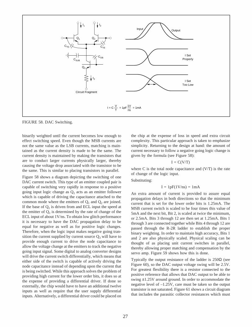
binarily weighted until the current becomes low enough toeffect switching speed. Even though the MSB currents arenot the same value as the LSB currents, matching is main-tained as the current density is made to be the same. Thecurrent density is maintained by making the transistors thatare to conduct larger currents physically larger, therebycausing the voltage drop associated with the transistor to bethe same. This is similar to placing transistors in parallel.
Figure 58 shows a diagram depicting the switching of oneDAC current switch. This type of an emitter coupled pair iscapable of switching very rapidly in response to a positivegoing input logic change as Q1 acts as an emitter followerwhich is capable of driving the capacitance attached to thecommon mode where the emitters of Q1 and Q2 are joined.If the base of Q1 is driven from and ECL input the speed atthe emitter of Q1 is determined by the rate of change of theECL input of about 1V/ns. To obtain low glitch performanceit is necessary to have the DAC propagation delay to beequal for negative as well as for positive logic changes.Therefore, when the logic input makes negative going tran-sition the current supplied by current source Q3 will have toprovide enough current to drive the node capacitance toallow the voltage change at the emitters to track the negativegoing input signal. Some digital to analog converter designswill drive the current switch differentially, which means thateither side of the switch is capable of actively driving thenode capacitance instead of depending upon the current thatis being switched. While this approach solves the problem ofproviding high current for the lower order bits, it does so atthe expense of providing a differential driver. If done soexternally, the chip would have to have an additional twelveinputs as well as require that the user supply differentialinputs. Alternatively, a differential driver could be placed on
the chip at the expense of loss in speed and extra circuitcomplexity. This particular approach is taken to emphasizesimplicity. Returning to the design at hand: the amount ofcurrent necessary to follow a negative going logic change isgiven by the formula (see Figure 58):
I = C(V/T)
where C is the total node capacitance and (V/T) is the rateof change of the logic input.
Substituting:
I = 1pF(1V/ns) = 1mA
An extra amount of current is provided to assure equalpropagation delays in both directions so that the minimumcurrent that is set for the lower order bits is 1.25mA. TheMSB current switch is scaled to be four times this value of5mA and the next bit, Bit 2, is scaled at twice the minimum,or 2.5mA. Bits 3 through 12 are then set at 1.25mA. Bits 1through 3 are connected together while Bits 4 through 12 arepassed through the R-2R ladder to establish the properbinary weighting. In order to maintain high accuracy, Bits 1and 2 are also physically scaled. Physical scaling can bethought of as placing unit current switches in parallel,thereby allowing proper matching and compensation by theservo amp. Figure 59 shows how this is done.
Typically the output resistance of the ladder is 250Ω (seeFigure 60), so the DAC output voltage swing will be 2.5V.For greatest flexibility there is a resistor connected to thepositive reference that allows that DAC output to be able toswing ±1.25V around ground. In order to accommodate thenegative level of –1.25V, care must be taken so the outputtransistor is not saturated. Figure 61 shows a circuit diagramthat includes the parasitic collector resistances which must
Input
Circuit Fragment
Q3
Q2Q1
I3
I = CVT
= 1mA
COBCSUB
CTECTE
Output
I SetProperly
I SetToo Low
= 1pF1Vns
I1 I2
FIGURE 58. DAC Switching.
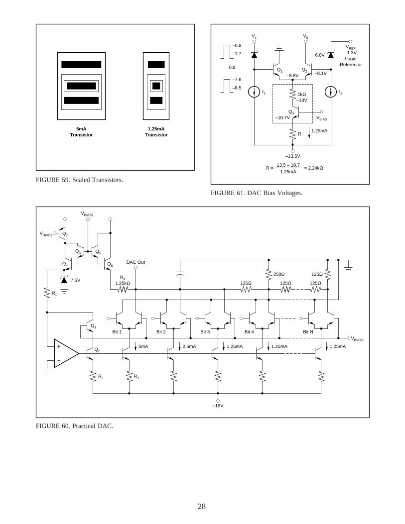
28
FIGURE 61. DAC Bias Voltages.
FIGURE 60. Practical DAC.
5mATransistor
1.25mATransistor
FIGURE 59. Scaled Transistors.
R
VREF–1.3VLogic
Reference
–13.5V
Q3VBIAS–10.7V
1kΩ–10V
–8.8V –8.1V
6.8V
Q2Q1
1.25mA
–0.8
–1.7
–7.6
–8.5
6.8
R =13.5 – 10.7
1.25mA= 2.24kΩ
V1
I1 I2
V0
DAC Out
R41.25kΩ 125Ω 125Ω
125Ω
125Ω
250Ω
5mA 2.5mA 1.25mA 1.25mA 1.25mA
–15V
VBIAS1
7.5V
Bit 1 Bit 2 Bit 3 Bit 4 Bit N
R2 R3
R1
Q4 Q6
Q5Q3
Q7
Q1
Q2
VBIAS2
VBIAS3
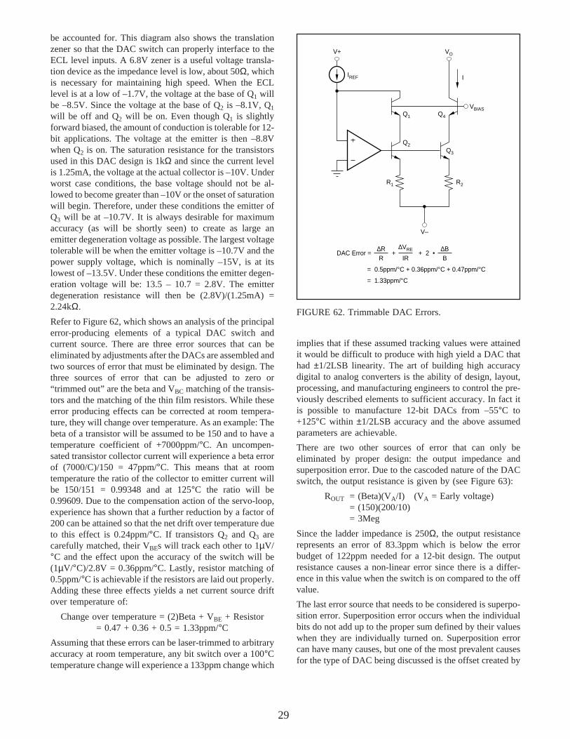
29
be accounted for. This diagram also shows the translationzener so that the DAC switch can properly interface to theECL level inputs. A 6.8V zener is a useful voltage transla-tion device as the impedance level is low, about 50Ω, whichis necessary for maintaining high speed. When the ECLlevel is at a low of –1.7V, the voltage at the base of Q1 willbe –8.5V. Since the voltage at the base of Q2 is –8.1V, Q1
will be off and Q2 will be on. Even though Q1 is slightlyforward biased, the amount of conduction is tolerable for 12-bit applications. The voltage at the emitter is then –8.8Vwhen Q2 is on. The saturation resistance for the transistorsused in this DAC design is 1kΩ and since the current levelis 1.25mA, the voltage at the actual collector is –10V. Underworst case conditions, the base voltage should not be al-lowed to become greater than –10V or the onset of saturationwill begin. Therefore, under these conditions the emitter ofQ3 will be at –10.7V. It is always desirable for maximumaccuracy (as will be shortly seen) to create as large anemitter degeneration voltage as possible. The largest voltagetolerable will be when the emitter voltage is –10.7V and thepower supply voltage, which is nominally –15V, is at itslowest of –13.5V. Under these conditions the emitter degen-eration voltage will be: 13.5 – 10.7 = 2.8V. The emitterdegeneration resistance will then be (2.8V)/(1.25mA) =2.24kΩ.
Refer to Figure 62, which shows an analysis of the principalerror-producing elements of a typical DAC switch andcurrent source. There are three error sources that can beeliminated by adjustments after the DACs are assembled andtwo sources of error that must be eliminated by design. Thethree sources of error that can be adjusted to zero or“trimmed out” are the beta and VBC matching of the transis-tors and the matching of the thin film resistors. While theseerror producing effects can be corrected at room tempera-ture, they will change over temperature. As an example: Thebeta of a transistor will be assumed to be 150 and to have atemperature coefficient of +7000ppm/°C. An uncompen-sated transistor collector current will experience a beta errorof (7000/C)/150 = 47ppm/°C. This means that at roomtemperature the ratio of the collector to emitter current willbe 150/151 = 0.99348 and at 125°C the ratio will be0.99609. Due to the compensation action of the servo-loop,experience has shown that a further reduction by a factor of200 can be attained so that the net drift over temperature dueto this effect is 0.24ppm/°C. If transistors Q2 and Q3 arecarefully matched, their VBEs will track each other to 1µV/°C and the effect upon the accuracy of the switch will be(1µV/°C)/2.8V = 0.36ppm/°C. Lastly, resistor matching of0.5ppm/°C is achievable if the resistors are laid out properly.Adding these three effects yields a net current source driftover temperature of:
Change over temperature = (2)Beta + VBE + Resistor= 0.47 + 0.36 + 0.5 = 1.33ppm/°C
Assuming that these errors can be laser-trimmed to arbitraryaccuracy at room temperature, any bit switch over a 100°Ctemperature change will experience a 133ppm change which
implies that if these assumed tracking values were attainedit would be difficult to produce with high yield a DAC thathad ±1/2LSB linearity. The art of building high accuracydigital to analog converters is the ability of design, layout,processing, and manufacturing engineers to control the pre-viously described elements to sufficient accuracy. In fact itis possible to manufacture 12-bit DACs from –55°C to+125°C within ±1/2LSB accuracy and the above assumedparameters are achievable.
There are two other sources of error that can only beeliminated by proper design: the output impedance andsuperposition error. Due to the cascoded nature of the DACswitch, the output resistance is given by (see Figure 63):
ROUT = (Beta)(VA/I) (VA = Early voltage)= (150)(200/10)= 3Meg
Since the ladder impedance is 250Ω, the output resistancerepresents an error of 83.3ppm which is below the errorbudget of 122ppm needed for a 12-bit design. The outputresistance causes a non-linear error since there is a differ-ence in this value when the switch is on compared to the offvalue.
The last error source that needs to be considered is superpo-sition error. Superposition error occurs when the individualbits do not add up to the proper sum defined by their valueswhen they are individually turned on. Superposition errorcan have many causes, but one of the most prevalent causesfor the type of DAC being discussed is the offset created by
FIGURE 62. Trimmable DAC Errors.
R2R1
IREF
VBIAS
Q2
Q1 Q4
Q3
I
V–
DAC Error =∆RR
+∆VRE
IR+ 2 •
∆BB
= 0.5ppm/°C + 0.36ppm/°C + 0.47ppm/°C
= 1.33ppm/°C
V+ VO
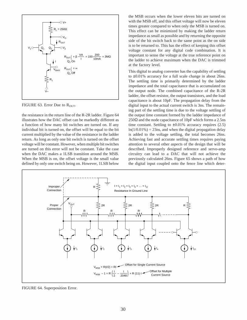
30
the MSB occurs when the lower eleven bits are turned onwith the MSB off, and this offset voltage will now be eleventimes greater compared to when only the MSB is turned on.This effect can be minimized by making the ladder returnimpedance as small as possible and by returning the oppositeside of the bit switch back to the same point as the on sideis to be returned to. This has the effect of keeping this offsetvoltage constant for any digital code combination. It isimportant to sense the voltage at the true reference point onthe ladder to achieve maximum when the DAC is trimmedat the factory level.
This digital to analog converter has the capability of settlingto ±0.01% accuracy for a full scale change in about 26ns.The settling time is primarily determined by the ladderimpedance and the total capacitance that is accumulated onthe output node. The combined capacitance of the R-2Rladder, the offset resistor, the output transistors, and the loadcapacitance is about 10pF. The propagation delay from thedigital input to the actual current switch is 3ns. The remain-ing part of the settling time is due to the voltage settling ofthe output time constant formed by the ladder impedance of250Ω and the node capacitance of 10pF which forms a 2.5nstime constant. Settling to ±0.01% accuracy requires (2.5)ln(1/0.01%) = 23ns, and when the digital propagation delayis added to the voltage settling, the total becomes 26ns.Achieving fast and accurate settling times requires payingattention to several other aspects of the design that will bedescribed. Improperly designed reference and servo-ampcircuitry can lead to a DAC that will not achieve thepreviously calculated 26ns. Figure 65 shows a path of howthe digital input coupled onto the fence line which deter-
FIGURE 63. Error Due to ROUT.
the resistance in the return line of the R-2R ladder. Figure 64illustrates how the DAC offset can be markedly different asa function of how many bit switches are turned on. If anyindividual bit is turned on, the offset will be equal to the bitcurrent multiplied by the value of the resistance in the ladderreturn. As long as only one bit switch is turned on the offsetvoltage will be constant. However, when multiple bit switchesare turned on this error will not be constant. Take the casewhen the DAC makes a 1LSB transition around the MSB.When the MSB is on, the offset voltage is the small valuedefined by only one switch being on. However, 1LSB below
FIGURE 64. Superposition Error.
VOUT
R
I1
R R
2R 2R 2R R
I2 I3 I4 I12
R I = I1 + I2 + I3 + I4 + … + I12
Resistance in Ground Line
VMSB = R(I/2) + RI
VMSB – 1 = R + R (11) II2 )( I
2048–
Offset for Single Current Source
Offset for MultipleCurrent Source
ProperConnection
ImproperConnection
Q1 Q2
RL = 250Ω
ROUT
I
ROUT = β
Q2 On
VAI
= 150200
10mA= 3MΩ
ROUT = ∞
Q2 Off
V2V1
VO
V+
R1
V–
VBIAS
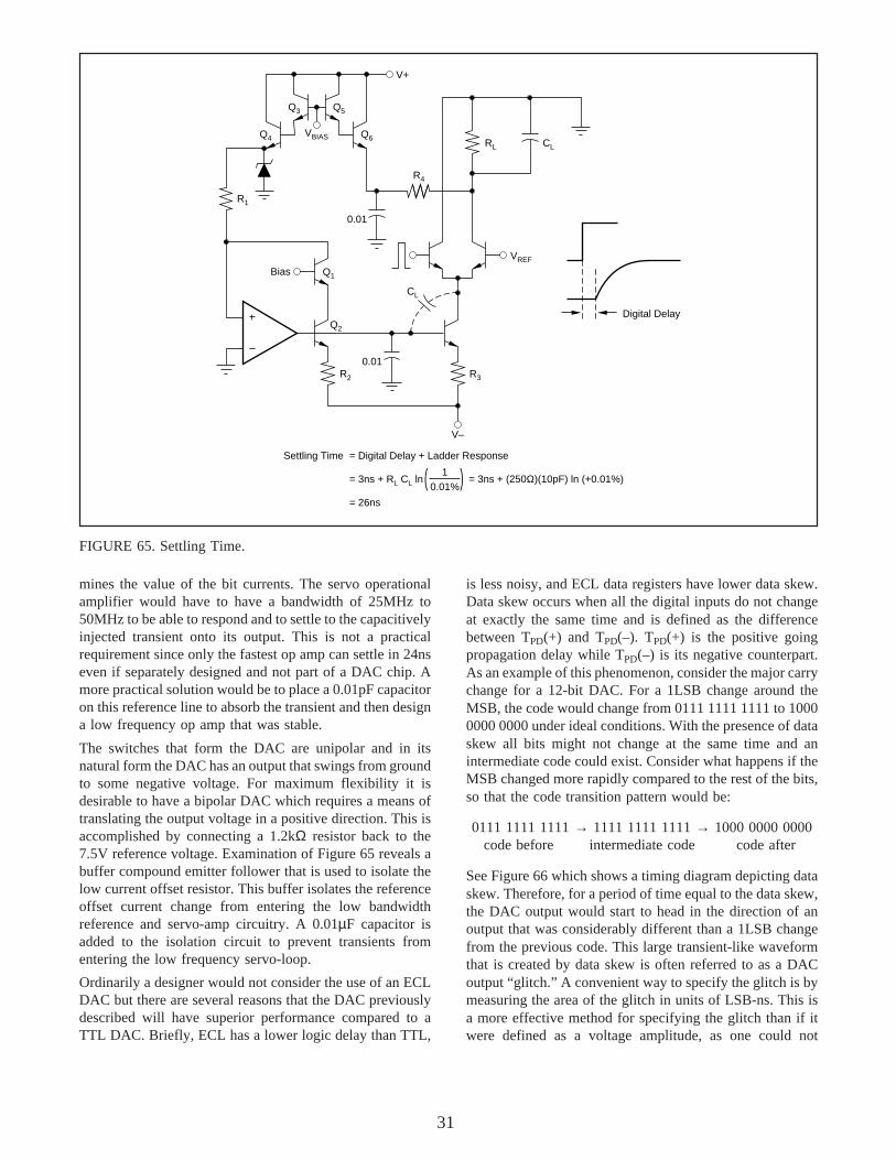
31
mines the value of the bit currents. The servo operationalamplifier would have to have a bandwidth of 25MHz to50MHz to be able to respond and to settle to the capacitivelyinjected transient onto its output. This is not a practicalrequirement since only the fastest op amp can settle in 24nseven if separately designed and not part of a DAC chip. Amore practical solution would be to place a 0.01pF capacitoron this reference line to absorb the transient and then designa low frequency op amp that was stable.
The switches that form the DAC are unipolar and in itsnatural form the DAC has an output that swings from groundto some negative voltage. For maximum flexibility it isdesirable to have a bipolar DAC which requires a means oftranslating the output voltage in a positive direction. This isaccomplished by connecting a 1.2kΩ resistor back to the7.5V reference voltage. Examination of Figure 65 reveals abuffer compound emitter follower that is used to isolate thelow current offset resistor. This buffer isolates the referenceoffset current change from entering the low bandwidthreference and servo-amp circuitry. A 0.01µF capacitor isadded to the isolation circuit to prevent transients fromentering the low frequency servo-loop.
Ordinarily a designer would not consider the use of an ECLDAC but there are several reasons that the DAC previouslydescribed will have superior performance compared to aTTL DAC. Briefly, ECL has a lower logic delay than TTL,
is less noisy, and ECL data registers have lower data skew.Data skew occurs when all the digital inputs do not changeat exactly the same time and is defined as the differencebetween TPD(+) and TPD(–). TPD(+) is the positive goingpropagation delay while TPD(–) is its negative counterpart.As an example of this phenomenon, consider the major carrychange for a 12-bit DAC. For a 1LSB change around theMSB, the code would change from 0111 1111 1111 to 10000000 0000 under ideal conditions. With the presence of dataskew all bits might not change at the same time and anintermediate code could exist. Consider what happens if theMSB changed more rapidly compared to the rest of the bits,so that the code transition pattern would be:
0111 1111 1111 → 1111 1111 1111 → 1000 0000 0000code before intermediate code code after
See Figure 66 which shows a timing diagram depicting dataskew. Therefore, for a period of time equal to the data skew,the DAC output would start to head in the direction of anoutput that was considerably different than a 1LSB changefrom the previous code. This large transient-like waveformthat is created by data skew is often referred to as a DACoutput “glitch.” A convenient way to specify the glitch is bymeasuring the area of the glitch in units of LSB-ns. This isa more effective method for specifying the glitch than if itwere defined as a voltage amplitude, as one could not
FIGURE 65. Settling Time.
Bias
0.01
RL CL
0.01
CL
Digital Delay
= Digital Delay + Ladder Response
= 3ns + RL CL ln
= 26ns
= 3ns + (250Ω)(10pF) ln (+0.01%))( 10.01%
Settling Time
V–
Q5Q3
Q4 Q6
Q1
Q2
R2 R3
R1
V+
R4
VREF
VBIAS
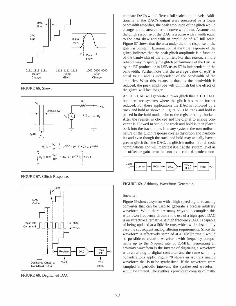
32
compare DACs with different full scale output levels. Addi-tionally, if the DAC’s output were processed by a lowerbandwidth amplifier, the peak amplitude of the glitch wouldchange but the area under the curve would not. Assume thatthe glitch response of the DAC is a pulse with a width equalto the data skew and with an amplitude of 1/2 full scale.Figure 67 shows that the area under the time response of theglitch is constant. Examination of the time response of theglitch indicates that the peak glitch amplitude is a functionof the bandwidth of the amplifier. For that reason, a morereliable way to specify the glitch performance of the DAC isby the ET product, or in LSB-ns as ET is independent of thebandwidth. Further note that the average value of eO(t) isequal to ET and is independent of the bandwidth of theamplifier. What this means is that, as the bandwidth isreduced, the peak amplitude will diminish but the effect ofthe glitch will last longer.
An ECL DAC will generate a lower glitch than a TTL DACbut there are systems where the glitch has to be furtherreduced. For these applications the DAC is followed by atrack and hold as shown in Figure 68. The track and hold isplaced in the hold mode prior to the register being clocked.After the register is clocked and the digital to analog con-verter is allowed to settle, the track and hold is then placedback into the track mode. In many systems the non-uniformnature of the glitch response creates distortion and harmon-ics and even though the track and hold may actually have agreater glitch than the DAC, the glitch is uniform for all codecombinations and will manifest itself at the system level asan offset or gain error but not as a code dependent non-
DigitalInput
0111 1111 1111Before
Change
1111 1111 1111DuringGlitch
1000 0000 0000After
Change
DataSkew
DACOut
DataSkew
FIGURE 66. Skew.
FIGURE 68. Deglitched DAC.
FIGURE 67. Glitch Response.
linearity.
Figure 69 shows a system with a high speed digital to analogconverter that can be used to generate a precise arbitrarywaveform. While there are many ways to accomplish thiswith lower frequency circuitry, the use of a high speed DACis an attractive alternative. A high frequency DAC is capableof being updated at a 50MHz rate, which will substantiallyease the subsequent analog filtering requirements. Since thewaveform is effectively sampled at a 50MHz rate it wouldbe possible to create a waveform with frequency compo-nents up to the Nyquist rate of 25MHz. Generating anarbitrary waveform is the inverse of digitizing a waveformwith an analog to digital converter and the same samplingconsiderations apply. Figure 70 shows an arbitrary analogwaveform that is to be synthesized. If the waveform weresampled at periodic intervals, the synthesized waveformwould be created. The synthesis procedure consists of math-
R1
C1VP
VOUT
i (t)
Data Skew
VP
TeO (t)
eO (t) =VP
R
T
Ct–(T/RC) = (VP T) • 2π fO e–2π fO t
eO (t) dt =VP T
RC• RC (1 – e–(T/RC)) = VP T
∞
o
∞
oROM DAC Track
HoldCounter
ClockFilter
FIGURE 69. Arbitrary Waveform Generator.
DACOutput
HoldTrack/HoldCommand
Register DAC TrackHold
Clock T/HSignal
Deglitched Output at Track/Hold Output
Track
Glitch
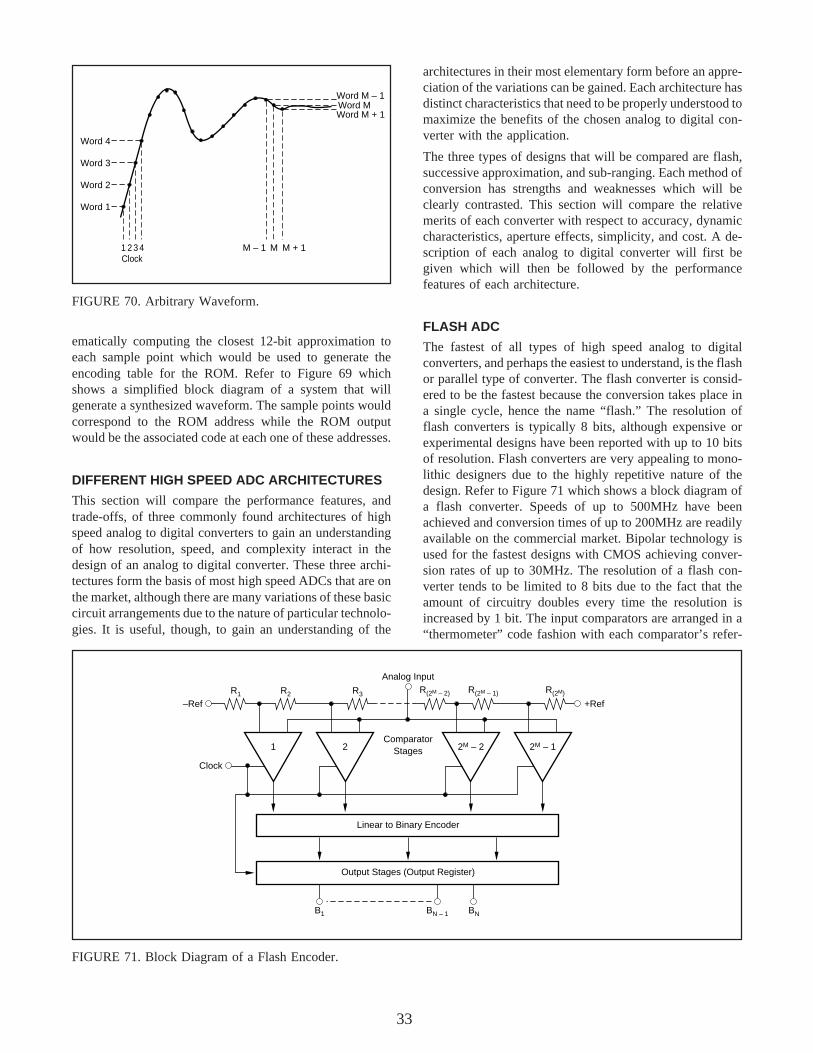
33
architectures in their most elementary form before an appre-ciation of the variations can be gained. Each architecture hasdistinct characteristics that need to be properly understood tomaximize the benefits of the chosen analog to digital con-verter with the application.
The three types of designs that will be compared are flash,successive approximation, and sub-ranging. Each method ofconversion has strengths and weaknesses which will beclearly contrasted. This section will compare the relativemerits of each converter with respect to accuracy, dynamiccharacteristics, aperture effects, simplicity, and cost. A de-scription of each analog to digital converter will first begiven which will then be followed by the performancefeatures of each architecture.
FLASH ADC
The fastest of all types of high speed analog to digitalconverters, and perhaps the easiest to understand, is the flashor parallel type of converter. The flash converter is consid-ered to be the fastest because the conversion takes place ina single cycle, hence the name “flash.” The resolution offlash converters is typically 8 bits, although expensive orexperimental designs have been reported with up to 10 bitsof resolution. Flash converters are very appealing to mono-lithic designers due to the highly repetitive nature of thedesign. Refer to Figure 71 which shows a block diagram ofa flash converter. Speeds of up to 500MHz have beenachieved and conversion times of up to 200MHz are readilyavailable on the commercial market. Bipolar technology isused for the fastest designs with CMOS achieving conver-sion rates of up to 30MHz. The resolution of a flash con-verter tends to be limited to 8 bits due to the fact that theamount of circuitry doubles every time the resolution isincreased by 1 bit. The input comparators are arranged in a“thermometer” code fashion with each comparator’s refer-
Word 1
Word 2
Word 3
Word 4
1 2 3 4
Word M + 1
M + 1
Word M
M
Word M – 1
M – 1Clock
FIGURE 70. Arbitrary Waveform.
ematically computing the closest 12-bit approximation toeach sample point which would be used to generate theencoding table for the ROM. Refer to Figure 69 whichshows a simplified block diagram of a system that willgenerate a synthesized waveform. The sample points wouldcorrespond to the ROM address while the ROM outputwould be the associated code at each one of these addresses.
DIFFERENT HIGH SPEED ADC ARCHITECTURES
This section will compare the performance features, andtrade-offs, of three commonly found architectures of highspeed analog to digital converters to gain an understandingof how resolution, speed, and complexity interact in thedesign of an analog to digital converter. These three archi-tectures form the basis of most high speed ADCs that are onthe market, although there are many variations of these basiccircuit arrangements due to the nature of particular technolo-gies. It is useful, though, to gain an understanding of the
FIGURE 71. Block Diagram of a Flash Encoder.
R2
1
R3
2
R(2M – 1)
2M – 2
R(2M)
2M – 1
R(2M – 2)
–Ref +Ref
Analog Input
R1
ComparatorStages
Linear to Binary Encoder
Output Stages (Output Register)
B1
Clock
BN – 1 BN
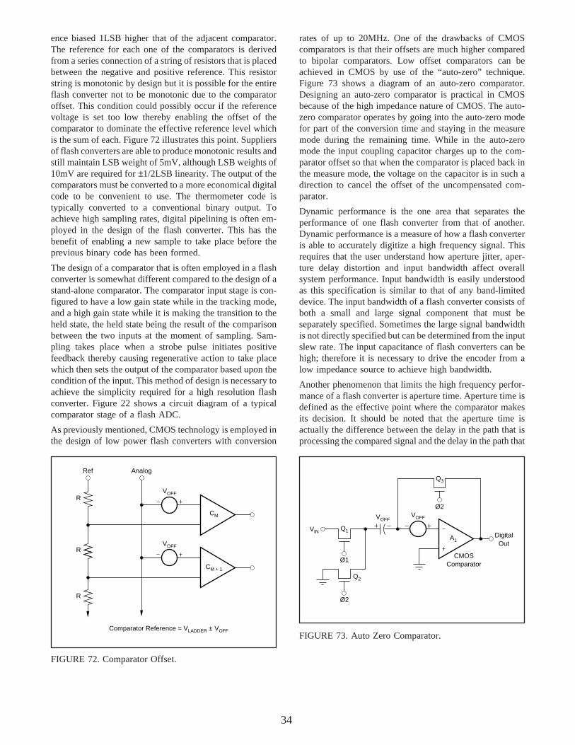
34
ence biased 1LSB higher that of the adjacent comparator.The reference for each one of the comparators is derivedfrom a series connection of a string of resistors that is placedbetween the negative and positive reference. This resistorstring is monotonic by design but it is possible for the entireflash converter not to be monotonic due to the comparatoroffset. This condition could possibly occur if the referencevoltage is set too low thereby enabling the offset of thecomparator to dominate the effective reference level whichis the sum of each. Figure 72 illustrates this point. Suppliersof flash converters are able to produce monotonic results andstill maintain LSB weight of 5mV, although LSB weights of10mV are required for ±1/2LSB linearity. The output of thecomparators must be converted to a more economical digitalcode to be convenient to use. The thermometer code istypically converted to a conventional binary output. Toachieve high sampling rates, digital pipelining is often em-ployed in the design of the flash converter. This has thebenefit of enabling a new sample to take place before theprevious binary code has been formed.
The design of a comparator that is often employed in a flashconverter is somewhat different compared to the design of astand-alone comparator. The comparator input stage is con-figured to have a low gain state while in the tracking mode,and a high gain state while it is making the transition to theheld state, the held state being the result of the comparisonbetween the two inputs at the moment of sampling. Sam-pling takes place when a strobe pulse initiates positivefeedback thereby causing regenerative action to take placewhich then sets the output of the comparator based upon thecondition of the input. This method of design is necessary toachieve the simplicity required for a high resolution flashconverter. Figure 22 shows a circuit diagram of a typicalcomparator stage of a flash ADC.
As previously mentioned, CMOS technology is employed inthe design of low power flash converters with conversion
rates of up to 20MHz. One of the drawbacks of CMOScomparators is that their offsets are much higher comparedto bipolar comparators. Low offset comparators can beachieved in CMOS by use of the “auto-zero” technique.Figure 73 shows a diagram of an auto-zero comparator.Designing an auto-zero comparator is practical in CMOSbecause of the high impedance nature of CMOS. The auto-zero comparator operates by going into the auto-zero modefor part of the conversion time and staying in the measuremode during the remaining time. While in the auto-zeromode the input coupling capacitor charges up to the com-parator offset so that when the comparator is placed back inthe measure mode, the voltage on the capacitor is in such adirection to cancel the offset of the uncompensated com-parator.
Dynamic performance is the one area that separates theperformance of one flash converter from that of another.Dynamic performance is a measure of how a flash converteris able to accurately digitize a high frequency signal. Thisrequires that the user understand how aperture jitter, aper-ture delay distortion and input bandwidth affect overallsystem performance. Input bandwidth is easily understoodas this specification is similar to that of any band-limiteddevice. The input bandwidth of a flash converter consists ofboth a small and large signal component that must beseparately specified. Sometimes the large signal bandwidthis not directly specified but can be determined from the inputslew rate. The input capacitance of flash converters can behigh; therefore it is necessary to drive the encoder from alow impedance source to achieve high bandwidth.
Another phenomenon that limits the high frequency perfor-mance of a flash converter is aperture time. Aperture time isdefined as the effective point where the comparator makesits decision. It should be noted that the aperture time isactually the difference between the delay in the path that isprocessing the compared signal and the delay in the path that
CM + 1
Ref Analog
VOFFR
CM
VOFFR
R
Comparator Reference = VLADDER ± VOFF
FIGURE 72. Comparator Offset.
CMOSComparator
VOFF
Ø2
Ø1
Ø2
DigitalOut
VIN
VOFF
Q3
A1
Q1
Q2
FIGURE 73. Auto Zero Comparator.
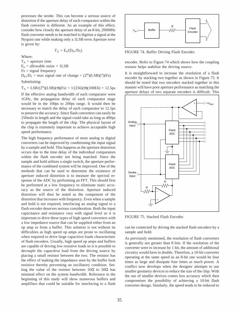
35
processes the strobe. This can become a serious source ofdistortion if the aperture delay of each comparator within theflash converter is different. As an example of this effect,consider how closely the aperture delay of an 8-bit, 200MHzflash converter needs to be matched to digitize a signal at theNyquist rate while making only a 1LSB error.Aperture erroris given by:
TA = En/(DFs/DT)
Where:TA = aperture timeEn = allowable noise = 1LSBFs = signal frequencyDFs/DT = max signal rate of change = (2N)(LSB)(7)(Fs)
Substituting:
TA = LSB/(2N)(LSB)(π)(Fs) = 1/(256)(π)(100E6) = 12.5ps
If the effective analog bandwidth of each comparator were1GHz, the propagation delay of each comparator stagewould be in the 100ps to 200ps range. It would then benecessary to match the delay of each comparator to 12.5psto preserve the accuracy. Since flash converters can easily be250mils in length and the signal could take as long as 400psto propagate the length of the chip. The physical layout ofthe chip is extremely important to achieve acceptable highspeed performance.
The high frequency performance of most analog to digitalconverters can be improved by conditioning the input signalby a sample and hold. This happens as the aperture distortionoccurs due to the time delay of the individual comparatorswithin the flash encoder not being matched. Since thesample and hold utilizes a single switch, the aperture perfor-mance of the combined system will be improved. One of themethods that can be used to determine the existence ofaperture induced distortion is to measure the spectral re-sponse of the ADC by performing an FFT. This should firstbe performed at a low frequency to eliminate static accu-racy as the source of the distortion. Aperture induceddistortion will then be noted as the component of thedistortion that increases with frequency. Even when a sampleand hold is not required, interfacing an analog signal to aflash encoder deserves serious consideration. Both the inputcapacitance and resistance vary with signal level so it isimportant to drive these types of high speed converters witha low impedance source that can be supplied either from anop amp or from a buffer. This solution is not without itsdifficulties as high speed op amps are prone to oscillatingwhen required to drive large capacitive loads characteristicof flash encoders. Usually, high speed op amps and buffersare capable of driving low resistive loads so it is possible todecouple the capacitive load from the driving source byplacing a small resistor between the two. The resistor hasthe effect of making the impedance seen by the buffer lookresistive thereby preventing an oscillatory condition. Set-ting the value of the resistor between 10Ω to 50Ω hasminimal effect on the system bandwidth. Reference to thebeginning of this study will show numerous buffers andamplifiers that could be suitable for interfacing to a flash
can be connected by driving the stacked flash encoders by asample and hold.
As previously mentioned, the resolution of flash convertersis generally not greater than 8 bits. If the resolution of theconverter were to increase by 1 bit, the amount of additionalcircuitry would have to double. Therefore, a 10-bit converteroperating at the same speed as an 8-bit one would be fourtimes as large and dissipate four times as much power. Aconflict now develops when the designer attempts to usesmaller geometry devices to reduce the size of the chip. Withthe use of smaller devices comes less accuracy which thencompromises the possibility of achieving a 10-bit flashconverter design. Similarly, the speed tends to be reduced to
RBuffer Flash
EncoderVIN
FIGURE 74. Buffer Driving Flash Encoder.
R
R
AnalogInput
StrobeInput
+VREF
FlashADC
FlashADC
FIGURE 75. Stacked Flash Encoder.
encoder. Refer to Figure 74 which shows how the couplingresistor helps stabilize the driving source.
It is straightforward to increase the resolution of a flashencoder by stacking two together as shown in Figure 75. Itshould be noted that two encoders stacked together in thismanner will have poor aperture performance as matching theaperture delays of two separate encoders is difficult. This
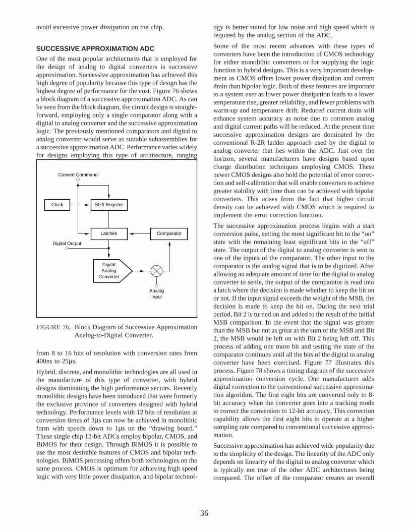
36
avoid excessive power dissipation on the chip.
SUCCESSIVE APPROXIMATION ADC
One of the most popular architectures that is employed forthe design of analog to digital converters is successiveapproximation. Successive approximation has achieved thishigh degree of popularity because this type of design has thehighest degree of performance for the cost. Figure 76 showsa block diagram of a successive approximation ADC. As canbe seen from the block diagram, the circuit design is straight-forward, employing only a single comparator along with adigital to analog converter and the successive approximationlogic. The previously mentioned comparators and digital toanalog converter would serve as suitable subassemblies fora successive approximation ADC. Performance varies widelyfor designs employing this type of architecture, ranging
ogy is better suited for low noise and high speed which isrequired by the analog section of the ADC.
Some of the most recent advances with these types ofconverters have been the introduction of CMOS technologyfor either monolithic converters or for supplying the logicfunction in hybrid designs. This is a very important develop-ment as CMOS offers lower power dissipation and currentdrain than bipolar logic. Both of these features are importantto a system user as lower power dissipation leads to a lowertemperature rise, greater reliability, and fewer problems withwarm-up and temperature drift. Reduced current drain willenhance system accuracy as noise due to common analogand digital current paths will be reduced. At the present timesuccessive approximation designs are dominated by theconventional R-2R ladder approach used by the digital toanalog converter that lies within the ADC. Just over thehorizon, several manufacturers have designs based uponcharge distribution techniques employing CMOS. Thesenewer CMOS designs also hold the potential of error correc-tion and self-calibration that will enable converters to achievegreater stability with time than can be achieved with bipolarconverters. This arises from the fact that higher circuitdensity can be achieved with CMOS which is required toimplement the error correction function.
The successive approximation process begins with a startconversion pulse, setting the most significant bit to the “on”state with the remaining least significant bits in the “off”state. The output of the digital to analog converter is sent toone of the inputs of the comparator. The other input to thecomparator is the analog signal that is to be digitized. Afterallowing an adequate amount of time for the digital to analogconverter to settle, the output of the comparator is read intoa latch where the decision is made whether to keep the bit onor not. If the input signal exceeds the weight of the MSB, thedecision is made to keep the bit on. During the next trialperiod, Bit 2 is turned on and added to the result of the initialMSB comparison. In the event that the signal was greaterthan the MSB but not as great as the sum of the MSB and Bit2, the MSB would be left on with Bit 2 being left off. Thisprocess of adding one more bit and testing the state of thecomparator continues until all the bits of the digital to analogconverter have been exercised. Figure 77 illustrates thisprocess. Figure 78 shows a timing diagram of the successiveapproximation conversion cycle. One manufacturer addsdigital correction to the conventional successive approxima-tion algorithm. The first eight bits are converted only to 8-bit accuracy when the converter goes into a tracking modeto correct the conversion to 12-bit accuracy. This correctioncapability allows the first eight bits to operate at a highersampling rate compared to conventional successive approxi-mation.
Successive approximation has achieved wide popularity dueto the simplicity of the design. The linearity of the ADC onlydepends on linearity of the digital to analog converter whichis typically not true of the other ADC architectures beingcompared. The offset of the comparator creates an overall
from 8 to 16 bits of resolution with conversion rates from400ns to 25µs.
Hybrid, discrete, and monolithic technologies are all used inthe manufacture of this type of converter, with hybriddesigns dominating the high performance sectors. Recentlymonolithic designs have been introduced that were formerlythe exclusive province of converters designed with hybridtechnology. Performance levels with 12 bits of resolution atconversion times of 3µs can now be achieved in monolithicform with speeds down to 1µs on the “drawing board.”These single chip 12-bit ADCs employ bipolar, CMOS, andBiMOS for their design. Through BiMOS it is possible touse the most desirable features of CMOS and bipolar tech-nologies. BiMOS processing offers both technologies on thesame process. CMOS is optimum for achieving high speedlogic with very little power dissipation, and bipolar technol-
FIGURE 76. Block Diagram of Successive ApproximationAnalog-to-Digital Converter.
AnalogInput
DigitalAnalog
Converter
Latches
Shift RegisterClock
Convert Command
Digital Output
Comparator
37
COMPARATOR DIGITALTRIAL DAC INPUT OUTPUT
1 2.048 0.072 12 2.048 + 1.024 –0.952 03 2.048 + 0.512 –0.440 04 2.048 + 0.256 –0.184 05 2.048 + 0.128 –0.056 06 2.048 + 0.064 +0.008 17 2.112 + 0.032 –0.024 08 2.112 + 0.016 –0.008 09 2.112 + 0.008 +0.000 110 2.120 + 0.004 –0.004 011 2.120 + 0.002 –0.002 012 2.120 + 0.001 –0.001 0
Analog In VIN
= 2.120VDigital Out 1000 0100 1000
offset but not a linearity error as would be created in a flashconverter. The state of the art in producing accurate digitalto analog converters is highly developed, which directlybenefits successive approximation converters. ADCs em-ploying these DACs will have correspondingly wide tem-perature ranges. Typically, successive approximation ADCswill operate over a wider temperature range, compared toother techniques, and designs are even available that operateat 200°C. Sub-ranging analog to digital converters haveadditional sources of error that distort the linearity, as will beexplained later. Since there is only a single comparator,more power can be applied to the DAC and comparator toreduce the overall conversion time. Additionally, a succes-sive approximation converter will naturally produce a serialform of the converted output. The serial output feature isvery useful for economical digital transmission. Also, itlends itself for optical isolation techniques which helpsreduce the interaction between the analog and digital sec-tions of the processing system. With this design, only theDAC has to settle to the final accuracy. This is not true of thesub-ranging arrangement as will be explained later. Assum-ing that the conversion rate could be achieved, successiveapproximation would be the architecture of choice as ahigher level or performance can be obtained at a givenselling price for a particular conversion rate. Another attrac-tive feature of successive approximation is that speed can beFIGURE 77. Successive Approximation Process.
FIGURE 78. Timing Diagram of a Successive Approximation Converter.
VIN = 2.120V
DAC
Logic
Comparator
DAC Full Scale = 4.096V
VO
Start
Bit 1
Bit 2
Bit 3
Bit 4
Bit 5
Bit 6
Bit 7
Bit 8
Bit 9
Bit 10
Bit 11
Bit 12
DAC
Comparator
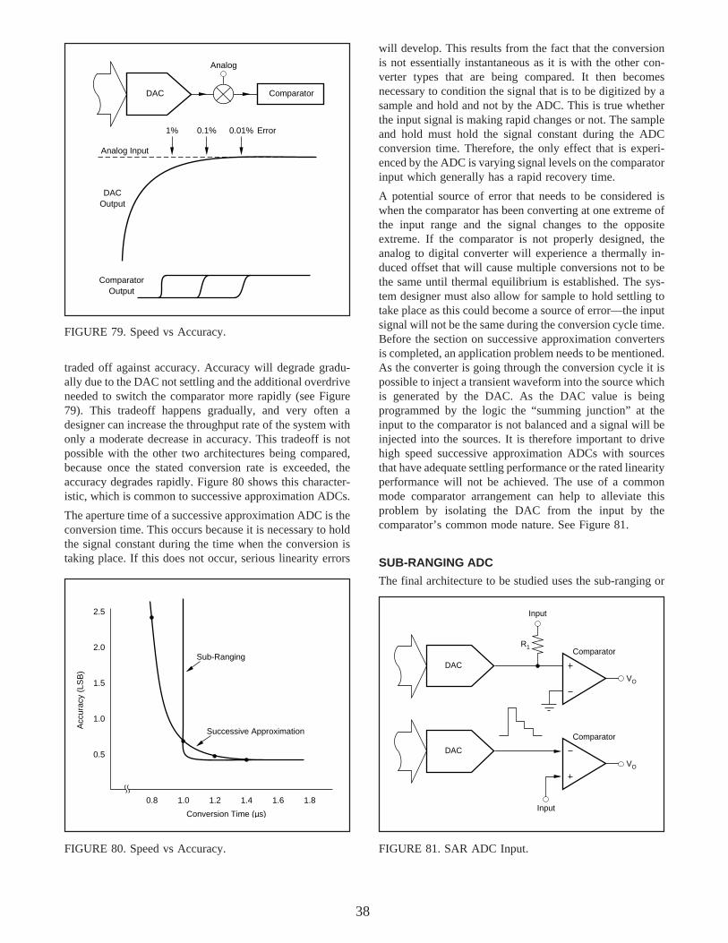
38
traded off against accuracy. Accuracy will degrade gradu-ally due to the DAC not settling and the additional overdriveneeded to switch the comparator more rapidly (see Figure79). This tradeoff happens gradually, and very often adesigner can increase the throughput rate of the system withonly a moderate decrease in accuracy. This tradeoff is notpossible with the other two architectures being compared,because once the stated conversion rate is exceeded, theaccuracy degrades rapidly. Figure 80 shows this character-istic, which is common to successive approximation ADCs.
The aperture time of a successive approximation ADC is theconversion time. This occurs because it is necessary to holdthe signal constant during the time when the conversion istaking place. If this does not occur, serious linearity errors
will develop. This results from the fact that the conversionis not essentially instantaneous as it is with the other con-verter types that are being compared. It then becomesnecessary to condition the signal that is to be digitized by asample and hold and not by the ADC. This is true whetherthe input signal is making rapid changes or not. The sampleand hold must hold the signal constant during the ADCconversion time. Therefore, the only effect that is experi-enced by the ADC is varying signal levels on the comparatorinput which generally has a rapid recovery time.
A potential source of error that needs to be considered iswhen the comparator has been converting at one extreme ofthe input range and the signal changes to the oppositeextreme. If the comparator is not properly designed, theanalog to digital converter will experience a thermally in-duced offset that will cause multiple conversions not to bethe same until thermal equilibrium is established. The sys-tem designer must also allow for sample to hold settling totake place as this could become a source of error—the inputsignal will not be the same during the conversion cycle time.Before the section on successive approximation convertersis completed, an application problem needs to be mentioned.As the converter is going through the conversion cycle it ispossible to inject a transient waveform into the source whichis generated by the DAC. As the DAC value is beingprogrammed by the logic the “summing junction” at theinput to the comparator is not balanced and a signal will beinjected into the sources. It is therefore important to drivehigh speed successive approximation ADCs with sourcesthat have adequate settling performance or the rated linearityperformance will not be achieved. The use of a commonmode comparator arrangement can help to alleviate thisproblem by isolating the DAC from the input by thecomparator’s common mode nature. See Figure 81.
SUB-RANGING ADC
The final architecture to be studied uses the sub-ranging or
FIGURE 80. Speed vs Accuracy. FIGURE 81. SAR ADC Input.
FIGURE 79. Speed vs Accuracy.
0.01%
DAC Comparator
0.1%1% Error
Analog Input
DACOutput
ComparatorOutput
Analog
2.5
2.0
1.5
1.0
0.5
Acc
urac
y (L
SB
)
0.8 1.0 1.2 1.4 1.6 1.8
Conversion Time (µs)
Sub-Ranging
Successive Approximation
DAC
Comparator
Input
DAC
Comparator
Input
VO
VO
R1
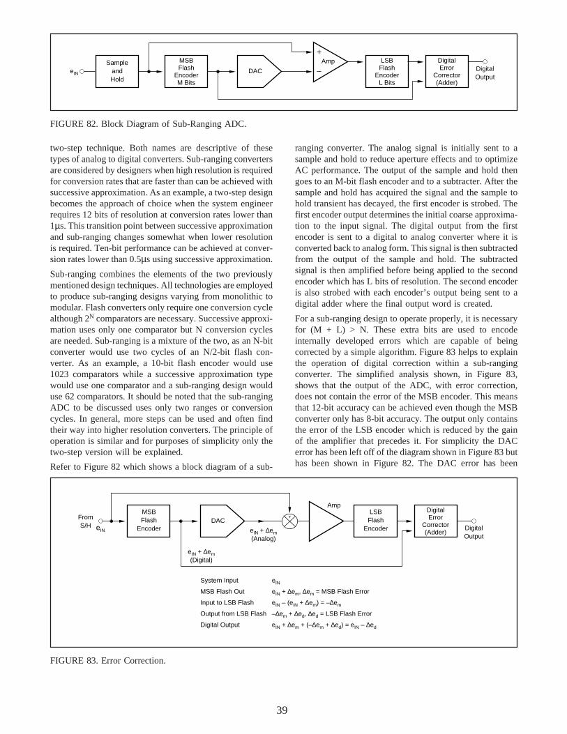
39
FIGURE 83. Error Correction.
two-step technique. Both names are descriptive of thesetypes of analog to digital converters. Sub-ranging convertersare considered by designers when high resolution is requiredfor conversion rates that are faster than can be achieved withsuccessive approximation. As an example, a two-step designbecomes the approach of choice when the system engineerrequires 12 bits of resolution at conversion rates lower than1µs. This transition point between successive approximationand sub-ranging changes somewhat when lower resolutionis required. Ten-bit performance can be achieved at conver-sion rates lower than 0.5µs using successive approximation.
Sub-ranging combines the elements of the two previouslymentioned design techniques. All technologies are employedto produce sub-ranging designs varying from monolithic tomodular. Flash converters only require one conversion cyclealthough 2N comparators are necessary. Successive approxi-mation uses only one comparator but N conversion cyclesare needed. Sub-ranging is a mixture of the two, as an N-bitconverter would use two cycles of an N/2-bit flash con-verter. As an example, a 10-bit flash encoder would use1023 comparators while a successive approximation typewould use one comparator and a sub-ranging design woulduse 62 comparators. It should be noted that the sub-rangingADC to be discussed uses only two ranges or conversioncycles. In general, more steps can be used and often findtheir way into higher resolution converters. The principle ofoperation is similar and for purposes of simplicity only thetwo-step version will be explained.
Refer to Figure 82 which shows a block diagram of a sub-
ranging converter. The analog signal is initially sent to asample and hold to reduce aperture effects and to optimizeAC performance. The output of the sample and hold thengoes to an M-bit flash encoder and to a subtracter. After thesample and hold has acquired the signal and the sample tohold transient has decayed, the first encoder is strobed. Thefirst encoder output determines the initial coarse approxima-tion to the input signal. The digital output from the firstencoder is sent to a digital to analog converter where it isconverted back to analog form. This signal is then subtractedfrom the output of the sample and hold. The subtractedsignal is then amplified before being applied to the secondencoder which has L bits of resolution. The second encoderis also strobed with each encoder’s output being sent to adigital adder where the final output word is created.
For a sub-ranging design to operate properly, it is necessaryfor (M + L) > N. These extra bits are used to encodeinternally developed errors which are capable of beingcorrected by a simple algorithm. Figure 83 helps to explainthe operation of digital correction within a sub-rangingconverter. The simplified analysis shown, in Figure 83,shows that the output of the ADC, with error correction,does not contain the error of the MSB encoder. This meansthat 12-bit accuracy can be achieved even though the MSBconverter only has 8-bit accuracy. The output only containsthe error of the LSB encoder which is reduced by the gainof the amplifier that precedes it. For simplicity the DACerror has been left off of the diagram shown in Figure 83 buthas been shown in Figure 82. The DAC error has been
FIGURE 82. Block Diagram of Sub-Ranging ADC.
DAC
AmpSampleandHold
DigitalError
Corrector(Adder)
DigitalOutput
LSBFlash
EncoderL Bits
MSBFlash
EncoderM Bits
eIN
DAC
AmpDigitalError
Corrector(Adder)
DigitalOutput
LSBFlash
Encoder
MSBFlash
EncodereIN
FromS/H
+
eIN + ∆em(Analog)
eIN + ∆em(Digital)
System Input
MSB Flash Out
Input to LSB Flash
Output from LSB Flash
Digital Output
eIN
eIN + ∆em, ∆em = MSB Flash Error
eIN – (eIN + ∆em) = –∆em
–∆em + ∆ed, ∆ed = LSB Flash Error
eIN + ∆em + (–∆em + ∆ed) = eIN – ∆ed
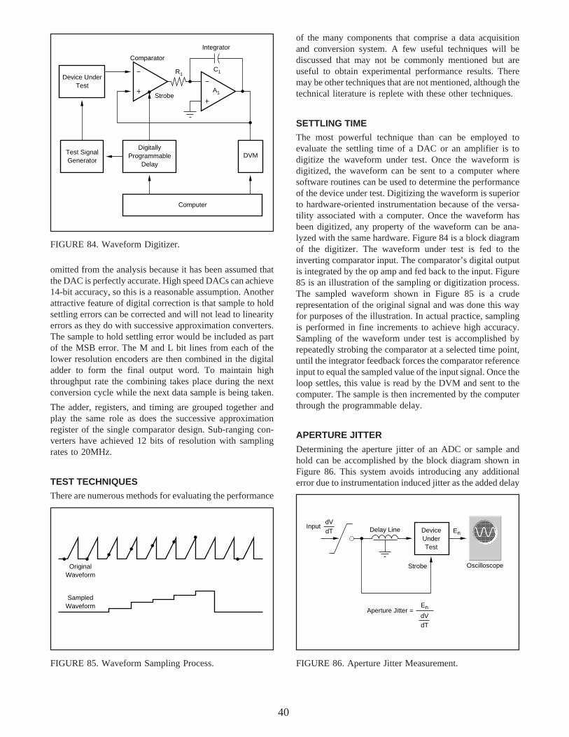
40
omitted from the analysis because it has been assumed thatthe DAC is perfectly accurate. High speed DACs can achieve14-bit accuracy, so this is a reasonable assumption. Anotherattractive feature of digital correction is that sample to holdsettling errors can be corrected and will not lead to linearityerrors as they do with successive approximation converters.The sample to hold settling error would be included as partof the MSB error. The M and L bit lines from each of thelower resolution encoders are then combined in the digitaladder to form the final output word. To maintain highthroughput rate the combining takes place during the nextconversion cycle while the next data sample is being taken.
The adder, registers, and timing are grouped together andplay the same role as does the successive approximationregister of the single comparator design. Sub-ranging con-verters have achieved 12 bits of resolution with samplingrates to 20MHz.
TEST TECHNIQUES
There are numerous methods for evaluating the performance
of the many components that comprise a data acquisitionand conversion system. A few useful techniques will bediscussed that may not be commonly mentioned but areuseful to obtain experimental performance results. Theremay be other techniques that are not mentioned, although thetechnical literature is replete with these other techniques.
SETTLING TIME
The most powerful technique than can be employed toevaluate the settling time of a DAC or an amplifier is todigitize the waveform under test. Once the waveform isdigitized, the waveform can be sent to a computer wheresoftware routines can be used to determine the performanceof the device under test. Digitizing the waveform is superiorto hardware-oriented instrumentation because of the versa-tility associated with a computer. Once the waveform hasbeen digitized, any property of the waveform can be ana-lyzed with the same hardware. Figure 84 is a block diagramof the digitizer. The waveform under test is fed to theinverting comparator input. The comparator’s digital outputis integrated by the op amp and fed back to the input. Figure85 is an illustration of the sampling or digitization process.The sampled waveform shown in Figure 85 is a cruderepresentation of the original signal and was done this wayfor purposes of the illustration. In actual practice, samplingis performed in fine increments to achieve high accuracy.Sampling of the waveform under test is accomplished byrepeatedly strobing the comparator at a selected time point,until the integrator feedback forces the comparator referenceinput to equal the sampled value of the input signal. Once theloop settles, this value is read by the DVM and sent to thecomputer. The sample is then incremented by the computerthrough the programmable delay.
APERTURE JITTER
Determining the aperture jitter of an ADC or sample andhold can be accomplished by the block diagram shown inFigure 86. This system avoids introducing any additionalerror due to instrumentation induced jitter as the added delay
FIGURE 84. Waveform Digitizer.
FIGURE 85. Waveform Sampling Process. FIGURE 86. Aperture Jitter Measurement.
Comparator
DigitallyProgrammable
Delay
Test SignalGenerator
Device UnderTest
Strobe
DVM
Integrator
Computer
R1C1
A1
DeviceUnderTest
dVdT
Input
Strobe
En
Oscilloscope
EnAperture Jitter =dVdT
Delay Line
OriginalWaveform
SampledWaveform
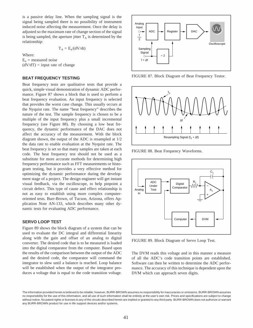
41
is a passive delay line. When the sampling signal is thesignal being sampled there is no possibility of instrumentinduced noise affecting the measurement. Once the delay isadjusted so the maximum rate of change section of the signalis being sampled, the aperture jitter TA is determined by therelationship:
TA = En/(dV/dt)
Where:En = measured noise(dV/dT) = input rate of change
BEAT FREQUENCY TESTING
Beat frequency tests are qualitative tests that provide aquick, simple visual demonstration of dynamic ADC perfor-mance. Figure 87 shows a block that is used to perform abeat frequency evaluation. An input frequency is selectedthat provides the worst case change. This usually occurs atthe Nyquist rate. The name “beat frequency” describes thenature of the test. The sample frequency is chosen to be amultiple of the input frequency plus a small incrementalfrequency (see Figure 88). By choosing a low beat fre-quency, the dynamic performance of the DAC does notaffect the accuracy of the measurement. With the blockdiagram shown, the output of the ADC is resampled at 1/2the data rate to enable evaluation at the Nyquist rate. Thebeat frequency is set so that many samples are taken at eachcode. The beat frequency test should not be used as asubstitute for more accurate methods for determining highfrequency performance such as FFT measurements or histo-gram testing, but it provides a very effective method foroptimizing the dynamic performance during the develop-ment stage of a project. The design engineer will get instantvisual feedback, via the oscilloscope, to help pinpoint acircuit defect. This type of cause and effect relationship isnot as easy to establish using more complex computer-oriented tests. Burr-Brown, of Tucson, Arizona, offers Ap-plication Note AN-133, which describes many other dy-namic tests for evaluating ADC performance.
SERVO LOOP TEST
Figure 89 shows the block diagram of a system that can beused to evaluate the DC integral and differential linearityalong with the gain and offset of an analog to digitalconverter. The desired code that is to be measured is loadedinto the digital comparator from the computer. Based uponthe results of the comparison between the output of the ADCand the desired code, the comparator will command theintegrator to slew until a balance is reached. Loop balancewill be established when the output of the integrator pro-duces a voltage that is equal to the code transition voltage.
DAC
Oscilloscope
f2
÷ 2
RegisterADC
AnalogInput
SamplingSignal
f + ∆f
FIGURE 87. Block Diagram of Beat Frequency Testor.
FIGURE 88. Beat Frequency Waveforms.
Resampling Signal (fS + ∆f)
fS
∆f
The information provided herein is believed to be reliable; however, BURR-BROWN assumes no responsibility for inaccuracies or omissions. BURR-BROWN assumesno responsibility for the use of this information, and all use of such information shall be entirely at the user’s own risk. Prices and specifications are subject to changewithout notice. No patent rights or licenses to any of the circuits described herein are implied or granted to any third party. BURR-BROWN does not authorize or warrantany BURR-BROWN product for use in life support devices and/or systems.
The DVM reads this voltage and in this manner a measureof all the ADC’s code transition points are established.Software can then be written to determine the ADC perfor-mance. The accuracy of this technique is dependent upon theDVM which can approach seven digits.
FIGURE 89. Block Diagram of Servo Loop Test.
DVM
DigitalComparator
ADCUnderTest
Computer
AnalogIn
R1
C1
A1

IMPORTANT NOTICE
Texas Instruments and its subsidiaries (TI) reserve the right to make changes to their products or to discontinueany product or service without notice, and advise customers to obtain the latest version of relevant informationto verify, before placing orders, that information being relied on is current and complete. All products are soldsubject to the terms and conditions of sale supplied at the time of order acknowledgment, including thosepertaining to warranty, patent infringement, and limitation of liability.
TI warrants performance of its semiconductor products to the specifications applicable at the time of sale inaccordance with TI’s standard warranty. Testing and other quality control techniques are utilized to the extentTI deems necessary to support this warranty. Specific testing of all parameters of each device is not necessarilyperformed, except those mandated by government requirements.
Customers are responsible for their applications using TI components.
In order to minimize risks associated with the customer’s applications, adequate design and operatingsafeguards must be provided by the customer to minimize inherent or procedural hazards.
TI assumes no liability for applications assistance or customer product design. TI does not warrant or representthat any license, either express or implied, is granted under any patent right, copyright, mask work right, or otherintellectual property right of TI covering or relating to any combination, machine, or process in which suchsemiconductor products or services might be or are used. TI’s publication of information regarding any thirdparty’s products or services does not constitute TI’s approval, warranty or endorsement thereof.
Copyright 2000, Texas Instruments Incorporated
Related Documents