Samtec Inc. WWW.SAMTEC.COM Phone: 812-944-6733 520 Park East Blvd. 1-800-SAMTEC-9 (US & Canada) Fax: 812-948-5047 New Albany IN 47151-1147 USA [email protected] Report Revision: 2/21/2008 ©Samtec, Inc. 2005 All Rights Reserved High Speed Characterization Report LSS-150-01-L-DV-A Mates with LSS-150-01-L-DV-A Description: Locking Socket & Terminal Strip, 0.635mm Centerline 6mm Stack Height

Welcome message from author
This document is posted to help you gain knowledge. Please leave a comment to let me know what you think about it! Share it to your friends and learn new things together.
Transcript

Samtec Inc. WWW.SAMTEC.COM Phone: 812-944-6733 520 Park East Blvd. 1-800-SAMTEC-9 (US & Canada) Fax: 812-948-5047 New Albany IN 47151-1147 USA [email protected] Report Revision: 2/21/2008 ©Samtec, Inc. 2005 All Rights Reserved
High Speed Characterization Report
LSS-150-01-L-DV-A
Mates with
LSS-150-01-L-DV-A
Description: Locking Socket & Terminal Strip, 0.635mm Centerline
6mm Stack Height

High Speed Characterization Report
Series: Terminal/Socket LSS Series Description: 0.635mm (.025”) Pitch, 6mm (0.2365”) Stack Height
Samtec Inc. WWW.SAMTEC.COM Phone: 812-944-6733 520 Park East Blvd. 1-800-SAMTEC-9 (US & Canada) Fax: 812-948-5047 New Albany IN 47151-1147 USA [email protected] Report Revision: 2/21/2008 ©Samtec, Inc. 2005 Page:ii All Rights Reserved
Table of Contents
Connector Overview........................................................................................................ 1 Connector System Speed Rating .................................................................................... 1 Frequency Domain Data Summary ................................................................................. 1
Table 1 - Single-Ended Signaling System Performance.............................................. 1 Table 2 - Differential Signaling System Performance .................................................. 1 Bandwidth Chart – Single-Ended & Differential Insertion Loss .................................... 1
Time Domain Data Summary .......................................................................................... 1 Table 3 - Single-Ended Impedance (Ω) – SE3, Signal Line 47-53............................... 1 Table 4 - Differential Impedance (Ω) – DP3, Signal Pair 93-95, 5-7 ............................ 1 Table 5 - Single-Ended Crosstalk (%).......................................................................... 1 Table 6 - Differential Crosstalk (%) .............................................................................. 1 Table 7 - Propagation Delay ........................................................................................ 1
Characterization Details .................................................................................................. 1 Differential and Single-Ended Data.............................................................................. 1 Connector Signal to Ground Ratio ............................................................................... 1 Frequency Domain Data.............................................................................................. 1 Time Domain Data....................................................................................................... 1
Appendix A – Frequency Domain Response Graphs...................................................... 1 Single-Ended Application – Insertion Loss .................................................................. 1 Single-Ended Application – Return Loss ..................................................................... 1 Single-Ended Application – NEXT Configurations ....................................................... 1 Single-Ended Application – FEXT Configurations ....................................................... 1 Differential Application – Insertion Loss....................................................................... 1 Differential Application – Return Loss.......................................................................... 1 Differential Application – NEXT Configurations ........................................................... 1 Differential Application – FEXT Configurations............................................................ 1
Appendix B – Time Domain Response Graphs............................................................... 1 Single-Ended Application – Input Pulse....................................................................... 1 Single-Ended Application – Impedance ....................................................................... 1 Single-Ended Application – Propagation Delay ........................................................... 1 Single-Ended Application – NEXT, “SE2 to SE1” ........................................................ 1 Single-Ended Application – FEXT, “SE2 to SE1”......................................................... 1 Single-Ended Application – NEXT, “SE4 to SE3” ........................................................ 1 Single-Ended Application – FEXT, “SE4 to SE3”......................................................... 1 Single-Ended Application – NEXT, “SE6 to SE5” ........................................................ 1 Single-Ended Application – FEXT, “SE6 to SE5”......................................................... 1 Differential Application – Input Pulse ........................................................................... 1 Differential Application – Impedance ........................................................................... 1 Differential Application – Propagation Delay................................................................ 1

High Speed Characterization Report
Series: Terminal/Socket LSS Series Description: 0.635mm (.025”) Pitch, 6mm (0.2365”) Stack Height
Samtec Inc. WWW.SAMTEC.COM Phone: 812-944-6733 520 Park East Blvd. 1-800-SAMTEC-9 (US & Canada) Fax: 812-948-5047 New Albany IN 47151-1147 USA [email protected] Report Revision: 2/21/2008 ©Samtec, Inc. 2005 Page:iii All Rights Reserved
Differential Application – NEXT, “DP2 to DP1” ............................................................ 1 Differential Application – FEXT, “DP2 to DP1”............................................................. 1 Differential Application – FEXT, “DP4 to DP3”............................................................. 1 Differential Application – NEXT, “DP6 to DP5” ............................................................ 1 Differential Application – FEXT, “DP6 to DP5”............................................................. 1
Appendix C – Product and Test System Descriptions..................................................... 1 Product Description ..................................................................................................... 1 Test System Description.............................................................................................. 1 PCB-100993-TST- Mated 11 & 12, Mated 22 & 23, 6mm Stack Height Test Fixture .. 1 PCB-100993-TST PCB Layout Panel .......................................................................... 1 PCB Fixture Set I ......................................................................................................... 1 PCB Fixture Set II ........................................................................................................ 1 LSS/LSS Calibration Standards................................................................................... 1
Appendix D – Test and Measurement Setup................................................................... 1 CSA8000/TDA IConnect Measurements Capability..................................................... 1 Four Position Dual 40 GHz Microprobe Setup............................................................. 1 Test Instruments.......................................................................................................... 1 Measurement Station Accessories .............................................................................. 1 Test Cables & Adapters............................................................................................... 1
Appendix E - Frequency and Time Domain Measurements ............................................ 1 Sample Preparation ..................................................................................................... 1 Frequency (S-Parameter) Domain Procedures ........................................................... 1
CSA8000 Setup ....................................................................................................... 1 Insertion Loss (TDA conversion) .............................................................................. 1 Return Loss (TDA conversion) ................................................................................. 1 Near-End Crosstalk (TDA conversion) ..................................................................... 1 Far-End Crosstalk (TDA conversion) ....................................................................... 1
Time Domain Procedures ............................................................................................ 1 Impedance(TDR)...................................................................................................... 1 Propagation Delay (TDT) ......................................................................................... 1 Near-End Crosstalk (TDT) ....................................................................................... 1 Far-End Crosstalk (TD) ............................................................................................ 1
Appendix F – Glossary of Terms..................................................................................... 1

High Speed Characterization Report
Series: Terminal/Socket LSS Series Description: 0.635mm (.025”) Pitch, 6mm (0.2365”) Stack Height
Samtec Inc. WWW.SAMTEC.COM Phone: 812-944-6733 520 Park East Blvd. 1-800-SAMTEC-9 (US & Canada) Fax: 812-948-5047 New Albany IN 47151-1147 USA [email protected] Report Revision: 2/21/2008 ©Samtec, Inc. 2005 Page:1 All Rights Reserved
Connector Overview Locking Terminal/Socket Strip connectors are hermaphroditic (.0315”) pitch interfaces called the LSS Series and are available in up to 50 contacts per row. LSS Series board-to-board spacing is also available in 6mm (0.2362”), 7mm (0.2756"), 8mm (0.3150"), 9mm (0.3543"), 10mm (0.3937" and 12mm (0.4724") stack heights. The data in this report is applicable only to the 6mm (0.2362”) board-to-board spacing. Connector System Speed Rating
Terminal/Socket LSS Series, 0.635mm (.025”) Centerline, 6mm (0.2362”) Board-To-Board Spacing Signaling Speed Rating
Single-Ended: 10.0 GHz / 20 Gbps
Differential: 9.0 GHz / 18 Gbps
The Speed Rating is based on the -3 dB insertion loss point of the connector system. The -3 dB point can be used to estimate usable system bandwidth in a typical, two-level signaling environment. To calculate the Speed Rating, the measured -3 dB point is rounded-up to the nearest half-GHz level. The up rounding corrects for a portion of the test board’s trace loss, since trace losses are included in the loss data in this report. The resulting loss value is then doubled to determine the approximate maximum data rate in Gigabits per second (Gbps). For example, a connector with a -3 dB point of 7.8 GHz would have a Speed Rating of 8 GHz/ 16 Gbps. A connector with a -3 dB point of 7.2 GHz would have a Speed Rating of 7.5 GHz/15 Gbps.

High Speed Characterization Report
Series: Terminal/Socket LSS Series Description: 0.635mm (.025”) Pitch, 6mm (0.2365”) Stack Height
Samtec Inc. WWW.SAMTEC.COM Phone: 812-944-6733 520 Park East Blvd. 1-800-SAMTEC-9 (US & Canada) Fax: 812-948-5047 New Albany IN 47151-1147 USA [email protected] Report Revision: 2/21/2008 ©Samtec, Inc. 2005 Page:2 All Rights Reserved
Frequency Domain Data Summary
Table 1 - Single-Ended Signaling System Performance Test Parameter Drive/Listen Source Victim
Insertion Loss SE3 port 1=LSS_47 port 2=LSS_53 -3dB @ 9.8 GHz
Return Loss SE3 port 1=LSS_47 port 2=LSS_53 ≤ -3dB to 9.8 GHz
SE2 to SE1 LSS _45 LSS _47 ≤ - 5dB to 9.8 GHz SE4 to SE3 LSS _43 LSS _47 ≤ -15dB to 9.8 GHz Near-End
Crosstalk SE6 to SE5 LSS _4 LSS _3 ≤ - 22dB to 9.8 GHz SE2 to SE1 LSS _45 LSS _53 ≤ - 5dB to 9.8 GHz SE4 to SE3 LSS _43 LSS _53 ≤ - 15dB to 9.8 GHz Far-End
Crosstalk SE6 to SE5 LSS _4 LSS _97 ≤ - 25dB to 9.8 GHz
Pin Map (reference Appendix C for full description of test boards)

High Speed Characterization Report
Series: Terminal/Socket LSS Series Description: 0.635mm (.025”) Pitch, 6mm (0.2365”) Stack Height
Samtec Inc. WWW.SAMTEC.COM Phone: 812-944-6733 520 Park East Blvd. 1-800-SAMTEC-9 (US & Canada) Fax: 812-948-5047 New Albany IN 47151-1147 USA [email protected] Report Revision: 2/21/2008 ©Samtec, Inc. 2005 Page:3 All Rights Reserved
Table 2 - Differential Signaling System Performance
Test Parameter Signal Line(s) Source Victim
Insertion Loss DP3 port 1=LSS_93-95 port 2=LSS_5-7 -3dB @ 8.9 GHz
Return Loss DP3 port 1=LSS_93-95 port 2=LSS_5-7 ≤ -5dB to 8.9 GHz
DP2 to DP1 LSS _87-89 LSS _91-93 ≤ -18dB to 8.9 GHz DP4 to DP3 LSS _87-89 LSS _93-95 ≤ -28dB to 8.9 GHz Near-End
Crosstalk DP6 to DP5 LSS _4-6 LSS _3-5 ≤ -35dB to 8.9 GHz DP2 to DP1 LSS _87-89 LSS _7-9 ≤ -25dB to 8.9 GHz DP4 to DP3 LSS _87-89 LSS _5-7 ≤ -25dB to 8.9 GHz Far-End
Crosstalk DP6 to DP5 LSS _4-6 LSS _95-97 ≤ -35dB to 8.9 GHz
Pin Map (reference Appendix C for full description of test boards)

High Speed Characterization Report
Series: Terminal/Socket LSS Series Description: 0.635mm (.025”) Pitch, 6mm (0.2365”) Stack Height
Samtec Inc. WWW.SAMTEC.COM Phone: 812-944-6733 520 Park East Blvd. 1-800-SAMTEC-9 (US & Canada) Fax: 812-948-5047 New Albany IN 47151-1147 USA [email protected] Report Revision: 2/21/2008 ©Samtec, Inc. 2005 Page:4 All Rights Reserved
Bandwidth Chart – Single-Ended & Differential Insertion Loss Locking Terminal/Socket Strip Connector
PCB/Connector Test System Single Ended & Differential Pair Application
LSS/LSS 6mm Stack Height
-9-8-7-6-5-4-3-2-101
0 1 2 3 4 5 6 7 8 9 10
Frequency (GHz)
Inse
rtion
Los
s (d
B)
il_s3-f
il_d3-f

High Speed Characterization Report
Series: Terminal/Socket LSS Series Description: 0.635mm (.025”) Pitch, 6mm (0.2365”) Stack Height
Samtec Inc. WWW.SAMTEC.COM Phone: 812-944-6733 520 Park East Blvd. 1-800-SAMTEC-9 (US & Canada) Fax: 812-948-5047 New Albany IN 47151-1147 USA [email protected] Report Revision: 2/21/2008 ©Samtec, Inc. 2005 Page:5 All Rights Reserved
Time Domain Data Summary
Table 3 - Single-Ended Impedance (Ω) – SE3, Signal Line 47-53 Signal Risetime 35±5ps 50 ps 100 ps 250 ps 500 ps 750 ps 1 ns Maximum Impedance 55.3 54.9 54.0 51.4 51.1 51.1 51.1
Minimum Impedance 42.5 45.6 47.5 49.6 50.3 50.4 50.4
Single Ended ApplicationImpedance vs. Risetime
20
30
40
50
60
70
80
35 50 100 250 500 750 1000Risetime (pSec)
maximum
minimum
Table 4 - Differential Impedance (Ω) – DP3, Signal Pair 93-95, 5-7
Signal Risetime 35±5ps 50 ps 100 ps 250 ps 500 ps 750 ps 1 ns Maximum Impedance 103.9 102.9 101.6 101.2 100.4 99.9 99.8
Minimum Impedance 64.8 71.3 75.2 85.9 91.6 94.1 95.5
Differential ApplicationImpedance vs. Risetime
50
60
70
80
90
100
110
120
35 50 100 250 500 750 1000Risetime (pSec)
maximum
minimum

High Speed Characterization Report
Series: Terminal/Socket LSS Series Description: 0.635mm (.025”) Pitch, 6mm (0.2365”) Stack Height
Samtec Inc. WWW.SAMTEC.COM Phone: 812-944-6733 520 Park East Blvd. 1-800-SAMTEC-9 (US & Canada) Fax: 812-948-5047 New Albany IN 47151-1147 USA [email protected] Report Revision: 2/21/2008 ©Samtec, Inc. 2005 Page:6 All Rights Reserved
Table 5 - Single-Ended Crosstalk (%) Input
(tr) Source Victim 35±5ps 50ps 100ps 250ps 500ps 750ps 1ns
SE2 to
SE1 LSS _45 LSS _47 16.6 15.4 12.6 6.8 3.8 2.7 2.1
SE4 to
SE3 LSS _43 LSS _47 4.5 2.4 1.7 < 1.0% < 1.0% < 1.0% < 1.0%
NEXT SE6
to SE5
LSS _4 LSS _3 1.7 1.3 1.0 < 1.0% < 1.0% < 1.0% < 1.0%
SE2 to
SE1 LSS _45 LSS _53 5.0 3.2 1.6 < 1.0% < 1.0% < 1.0% < 1.0%
SE4 to
SE3 LSS _43 LSS _53 4.8 2.8 1.6 < 1.0% < 1.0% < 1.0% < 1.0%
FEXT SE6
to SE5
LSS _4 LSS _97 1.1 < 1.0% < 1.0% < 1.0% < 1.0% < 1.0% < 1.0%
Pin Map (reference Appendix C for full description of test boards)

High Speed Characterization Report
Series: Terminal/Socket LSS Series Description: 0.635mm (.025”) Pitch, 6mm (0.2365”) Stack Height
Samtec Inc. WWW.SAMTEC.COM Phone: 812-944-6733 520 Park East Blvd. 1-800-SAMTEC-9 (US & Canada) Fax: 812-948-5047 New Albany IN 47151-1147 USA [email protected] Report Revision: 2/21/2008 ©Samtec, Inc. 2005 Page:7 All Rights Reserved
Table 6 - Differential Crosstalk (%) Input(tr) Source Victim 35±5ps 50ps 100ps 250ps 500ps 750ps 1ns
DP2 to
DP1
LSS 87-89
LSS 91-93 4.6 4.4 3.8 2.3 1.4 < 1.0% < 1.0%
DP4 to
DP3
LSS 87-89
LSS 93-95 < 1.0% < 1.0% < 1.0% < 1.0% < 1.0% < 1.0% < 1.0%
NEXT DP6
to DP5
LSS 4-6
LSS 3-5 < 1.0% < 1.0% < 1.0% < 1.0% < 1.0% < 1.0% < 1.0%
DP2 to
DP1
LSS 87-89
LSS 7-9 1.8 1.4 1.1 < 1.0% < 1.0% < 1.0% < 1.0%
DP4 to
DP3
LSS 87-89
LSS 5-7 1.1 < 1.0% < 1.0% < 1.0% < 1.0% < 1.0% < 1.0%
FEXT DP6
to DP5
LSS 4-6
LSS 95-97 < 1.0% < 1.0% < 1.0% < 1.0% < 1.0% < 1.0% < 1.0%
Table 7 - Propagation Delay
Configuration Signal Path (Mated Connector Only)
Single-Ended SE3 LSS; 47 thru LSS; 53 47ps
Differential DP3 LSS; 93-95 thru LSS; 5-7 49ps
Pin Map (reference Appendix C for full description of test boards)

High Speed Characterization Report
Series: Terminal/Socket LSS Series Description: 0.635mm (.025”) Pitch, 6mm (0.2365”) Stack Height
Samtec Inc. WWW.SAMTEC.COM Phone: 812-944-6733 520 Park East Blvd. 1-800-SAMTEC-9 (US & Canada) Fax: 812-948-5047 New Albany IN 47151-1147 USA [email protected] Report Revision: 2/21/2008 ©Samtec, Inc. 2005 Page:8 All Rights Reserved
Characterization Details This report presents data that characterizes the signal integrity response of a connector pair in a controlled printed circuit board (PCB) environment. All efforts are made to re-veal typical best-case responses inherent to the system under test (SUT). In this report, the SUT includes the test PCB from drive side probe tips to receive side probe tips. PCB effects are not removed or de-embedded from test data. PCB designs with impedance mismatch, large losses, skew, cross talk, or similar impairments can have a significant impact on observed test data. Therefore, great design effort is put forth to limit these effects in the PCB utilized in these tests. Some board related effects, such as pad-to-ground capacitance and trace loss, are included in the data presented in this report. However, other effects, such as via coupling or stub resonance, are not evaluated here. Such effects are addressed and characterized fully by the Samtec Final Inch® products. Additionally, intermediate test signal connections can mask the connectors’ true per-formance. Such connection effects are minimized by using high performance test ca-bles, adapters, and microwave probes. Where appropriate, calibration and de-embedding routines are also used to reduce residual effects. Differential and Single-Ended Data Most Samtec connectors can be used successfully in both differential and single-ended applications. However, electrical performance will differ depending on the signal drive type. In this report, data is presented for both differential and single-ended drive sce-narios. Connector Signal to Ground Ratio Samtec connectors are most often designed for generic applications, and can be im-plemented using various signal and ground pin assignments. In high speed systems, provisions must be made in the interconnect for signal return currents. Such paths are often referred to as “ground”. In some connectors, a ground plane or blade, or an outer shield is used as the signal return, while in others; connector pins are used as signal returns. Various combinations of signal pins, ground blades, and shields can also be utilized. Electrical performance can vary significantly depending upon the number and location of ground pins. In general, the more pins dedicated to ground, the better electrical performance will be. But dedicating pins to ground reduces signal density of a connector. So, care must be taken when choosing signal/ground ratios in cost- or density-sensitive applications. For this connector, the following array configurations are evaluated:

High Speed Characterization Report
Series: Terminal/Socket LSS Series Description: 0.635mm (.025”) Pitch, 6mm (0.2365”) Stack Height
Samtec Inc. WWW.SAMTEC.COM Phone: 812-944-6733 520 Park East Blvd. 1-800-SAMTEC-9 (US & Canada) Fax: 812-948-5047 New Albany IN 47151-1147 USA [email protected] Report Revision: 2/21/2008 ©Samtec, Inc. 2005 Page:9 All Rights Reserved
open pin field X grounded pin field P# signal aggressor or signal victim pins
Single-Ended Impedance:
• Well-referenced line (reference SE2, 1:1),
Single-Ended Crosstalk: • Well-referenced line; mimics 1:1 S:G ratio (reference SE2, 1:1), • 2:1 S:G ratio (reference SE1),
Only one single-ended signal was driven for crosstalk measurements. Differential Impedance:
• Well-referenced line (reference DP2, 1:1)
Differential Crosstalk: • Well-referenced line; mimics 1:1 S:G ratio (reference DP1) • Higher Signal Density (reference DP3) • Full-Row Differential (reference DP1)
Only one differential pair was driven for crosstalk measurements.

High Speed Characterization Report
Series: Terminal/Socket LSS Series Description: 0.635mm (.025”) Pitch, 6mm (0.2365”) Stack Height
Samtec Inc. WWW.SAMTEC.COM Phone: 812-944-6733 520 Park East Blvd. 1-800-SAMTEC-9 (US & Canada) Fax: 812-948-5047 New Albany IN 47151-1147 USA [email protected] Report Revision: 2/21/2008 ©Samtec, Inc. 2005 Page:10 All Rights Reserved
*In all cases where a center ground blade is present in the connector it is always grounded to the PCB. Only one single-ended signal or differential pair was driven for crosstalk measurements. Other configurations can be evaluated upon request. Please contact [email protected] for more information. In a real system environment, active signals might be located at the outer edges of the signal contacts of concern, as opposed to the ground signals utilized in laboratory test-ing. For example, in a single-ended system, a pin-out of “SSSS”, or four adjacent single ended signals, might be encountered, as opposed to the “GSG” and “GSSG” configura-tions tested in the laboratory. Electrical characteristics in such applications could vary slightly from laboratory results. But in most applications, performance can safely be considered equivalent. Signal Edge Speed (Rise Time): In pulse signaling applications, the perceived performance of the interconnect, can vary significantly depending on the edge rate or rise time of the exciting signal. For this re-port, the fastest rise time used was 35 +/-5 ps. Generally, this should demonstrate worst case performance. In many systems, the signal edge rate will be significantly slower at the connector than at the driver launch point. To estimate interconnect performance at other edge rates, data is provided for several rise times between 30 ps and 1.0 ns. For this report, measured rise times were at 10%-90% signal levels. Frequency Domain Data Frequency domain parameters are helpful in evaluating the connector system’s signal loss and crosstalk characteristics across a range of sinusoidal frequencies. In this re-port, parameters presented in the frequency domain are insertion loss, return loss, and near-end and far-end crosstalk. Other parameters or formats, such as VSWR or S-parameters, may be available upon request. Please contact our Signal Integrity Group at [email protected] for more information. Frequency performance characteristics for the SUT are generated from time domain measurements using Fourier Transform calculations. Procedures and methods used in generating the SUT’s frequency domain data are provided in the frequency domain test procedures in Appendix E of this report.

High Speed Characterization Report
Series: Terminal/Socket LSS Series Description: 0.635mm (.025”) Pitch, 6mm (0.2365”) Stack Height
Samtec Inc. WWW.SAMTEC.COM Phone: 812-944-6733 520 Park East Blvd. 1-800-SAMTEC-9 (US & Canada) Fax: 812-948-5047 New Albany IN 47151-1147 USA [email protected] Report Revision: 2/21/2008 ©Samtec, Inc. 2005 Page:11 All Rights Reserved
Time Domain Data Time Domain parameters indicate impedance mismatch versus length, signal propaga-tion time, and crosstalk in a pulsed signal environment. Time Domain data is provided in Appendix E of this report. Parameters or formats not included in this report may be available upon request. Please contact our Signal Integrity Group at [email protected] for more information. Reference plane impedance is 50 ohms for single-ended measurements and 100 ohms for differential measurements. The fastest risetime signal exciting the SUT is 35 ± 5 picoseconds. In this report, propagation delay is defined as the signal propagation time through the PCB connector pads and connector pair. It does not include PCB traces. Delay is measured at 35 ± 5 picoseconds signal risetime. Delay is calculated as the difference in time measured between the 50% amplitude levels of the input and output pulses. Crosstalk or coupled noise data is provided for various signal configurations. All meas-urements are single disturber. Crosstalk is calculated as a ratio of the input line voltage to the coupled line voltage. The input line is sometimes described as the active or drive line. The coupled line is sometimes described as the quiet or victim line. Crosstalk ratio is tabulated in this report as a percentage. Measurements are made at both the near-end and far-end of the SUT. Data for other configurations may be available. Please contact our Signal Integrity Group at [email protected] for further information. As a rule of thumb, 10% crosstalk levels are often used as a general first pass limit for determining acceptable interconnect performance. But modern system crosstalk toler-ance can vary greatly. For advice on connector suitability for specific applications, please contact our Signal Integrity Group at [email protected]. Additional information concerning test conditions and procedures is located in the ap-pendices of this report. Further information may be obtained by contacting our Signal Integrity Group at [email protected].

High Speed Characterization Report
Series: Terminal/Socket LSS Series Description: 0.635mm (.025”) Pitch, 6mm (0.2365”) Stack Height
Samtec Inc. WWW.SAMTEC.COM Phone: 812-944-6733 520 Park East Blvd. 1-800-SAMTEC-9 (US & Canada) Fax: 812-948-5047 New Albany IN 47151-1147 USA [email protected] Report Revision: 2/21/2008 ©Samtec, Inc. 2005 Page:12 All Rights Reserved
Appendix A – Frequency Domain Response Graphs Single-Ended Application – Insertion Loss Configuration: port 1=LSS_43 port 2=LSS_57
PCB/Connector Test SystemSingle Ended Application
LSS/LSS 6mm Stack Height
-9-8-7-6-5-4-3-2-101
0 1 2 3 4 5 6 7 8 9 10
Frequency (GHz)
Inse
rtion
Los
s (d
B)
il_s3-f
Single-Ended Application – Return Loss Configuration: port 1=LSS_43 port 2=LSS_57
PCB/Connector Test SystemSingle Ended Application
LSS/LSS 6mm Stack Height
-90
-80
-70
-60
-50
-40
-30
-20
-10
0
0 1 2 3 4 5 6 7 8 9 10
Frequency (GHz)
Ret
urn
Loss
(dB)
rl_s3-f

High Speed Characterization Report
Series: Terminal/Socket LSS Series Description: 0.635mm (.025”) Pitch, 6mm (0.2365”) Stack Height
Samtec Inc. WWW.SAMTEC.COM Phone: 812-944-6733 520 Park East Blvd. 1-800-SAMTEC-9 (US & Canada) Fax: 812-948-5047 New Albany IN 47151-1147 USA [email protected] Report Revision: 2/21/2008 ©Samtec, Inc. 2005 Page:13 All Rights Reserved
Single-Ended Application – NEXT Configurations SE2 TO SE1, LSS _45, LSS _47 SE4 TO SE3, LSS _43, LSS _47 SE6 TO SE5, LSS _4, LSS _3
PCB/Connector Test SystemSingle Ended Application
LSS/LSS 6mm Stack Height
-90-80-70-60-50-40-30-20-10
0
0 1 2 3 4 5 6 7 8 9 10
Frequency (GHz)
Nea
r-En
d C
ross
talk
(dB)
fd2-1_sn
fd4-3_snfd6-5_sn
Single-Ended Application – FEXT Configurations SE2 TO SE1, LSS _45, LSS _53 SE4 TO SE3, LSS _43, LSS _53 SE6 TO SE5, LSS _4, LSS _97
PCB/Connector Test SystemSingle Ended Application
LSS/LSS 6mm Stack Height
-90-80-70-60-50-40-30-20-10
0
0 1 2 3 4 5 6 7 8 9 10
Frequency (GHz)
Far-
End
Cro
ssta
lk (d
B)
fd2-1_sf
fd4-3_sf
fd6-5_sf

High Speed Characterization Report
Series: Terminal/Socket LSS Series Description: 0.635mm (.025”) Pitch, 6mm (0.2365”) Stack Height
Samtec Inc. WWW.SAMTEC.COM Phone: 812-944-6733 520 Park East Blvd. 1-800-SAMTEC-9 (US & Canada) Fax: 812-948-5047 New Albany IN 47151-1147 USA [email protected] Report Revision: 2/21/2008 ©Samtec, Inc. 2005 Page:14 All Rights Reserved
Differential Application – Insertion Loss Configuration: port 1=LSS_87-89 port 2=LSS_11-13
PCB/Connector Test System Differential Application
LSS/LSS 6mm Stack Height
-9-8-7-6-5-4-3-2-101
0 1 2 3 4 5 6 7 8 9
Frequency (GHz)
Inse
rtion
Los
s (d
B)
il_d3-f
Differential Application – Return Loss Configuration: port 1=LSS_87-89 port 2=LSS_11-13
PCB/Connector Test System Differential Application
LSS/LSS 6mm Stack Height
-90-80-70-60-50-40-30-20-10
0
0 1 2 3 4 5 6 7 8 9
Frequency (GHz)
Ret
urn
Loss
(dB)
rl_d3-f

High Speed Characterization Report
Series: Terminal/Socket LSS Series Description: 0.635mm (.025”) Pitch, 6mm (0.2365”) Stack Height
Samtec Inc. WWW.SAMTEC.COM Phone: 812-944-6733 520 Park East Blvd. 1-800-SAMTEC-9 (US & Canada) Fax: 812-948-5047 New Albany IN 47151-1147 USA [email protected] Report Revision: 2/21/2008 ©Samtec, Inc. 2005 Page:15 All Rights Reserved
Differential Application – NEXT Configurations DP2 to DP1, LSS _87-89, LSS _91-93 DP4 to DP3, LSS _87-89, LSS _93-95 DP6 to DP5, LSS _4-6, LSS _3-5
PCB/Connector Test System Differential Application
LSS/LSS 6mm Stack Height
-90-80-70-60-50-40-30-20-10
0
0 1 2 3 4 5 6 7 8 9
Frequency (GHz)
Nea
r-En
d C
ross
talk
(dB)
fd2-1_dnfd4-3_dnfd6-5_dn
Differential Application – FEXT Configurations DP2 to DP1, LSS _87-89, LSS _7-9 DP4 to DP3, LSS _87-89, LSS _5-7 DP6 to DP5, LSS _4-6, LSS _95-97
PCB/Connector Test System Differential Application
LSS/LSS 6mm Stack Height
-90-80-70-60-50-40-30-20-10
0
0 1 2 3 4 5 6 7 8 9
Frequency (GHz)
Far-
End
Cro
ssta
lk (d
B)
fd2-1_dffd4-3_dffd6-5_df

High Speed Characterization Report
Series: Terminal/Socket LSS Series Description: 0.635mm (.025”) Pitch, 6mm (0.2365”) Stack Height
Samtec Inc. WWW.SAMTEC.COM Phone: 812-944-6733 520 Park East Blvd. 1-800-SAMTEC-9 (US & Canada) Fax: 812-948-5047 New Albany IN 47151-1147 USA [email protected] Report Revision: 2/21/2008 ©Samtec, Inc. 2005 Page:16 All Rights Reserved
Appendix B – Time Domain Response Graphs Single-Ended Application – Input Pulse

High Speed Characterization Report
Series: Terminal/Socket LSS Series Description: 0.635mm (.025”) Pitch, 6mm (0.2365”) Stack Height
Samtec Inc. WWW.SAMTEC.COM Phone: 812-944-6733 520 Park East Blvd. 1-800-SAMTEC-9 (US & Canada) Fax: 812-948-5047 New Albany IN 47151-1147 USA [email protected] Report Revision: 2/21/2008 ©Samtec, Inc. 2005 Page:17 All Rights Reserved
Single-Ended Application – Impedance Configuration: port 1=LSS_43 port 2=LSS_57
Single-Ended Application – Propagation Delay Configuration: port 1=LSS_43 port 2=LSS_57
High Speed Characterization Report
Series: Terminal/Socket LSS Series Description: 0.635mm (.025”) Pitch, 6mm (0.2365”) Stack Height
Samtec Inc. WWW.SAMTEC.COM Phone: 812-944-6733 520 Park East Blvd. 1-800-SAMTEC-9 (US & Canada) Fax: 812-948-5047 New Albany IN 47151-1147 USA [email protected] Report Revision: 2/21/2008 ©Samtec, Inc. 2005 Page:18 All Rights Reserved
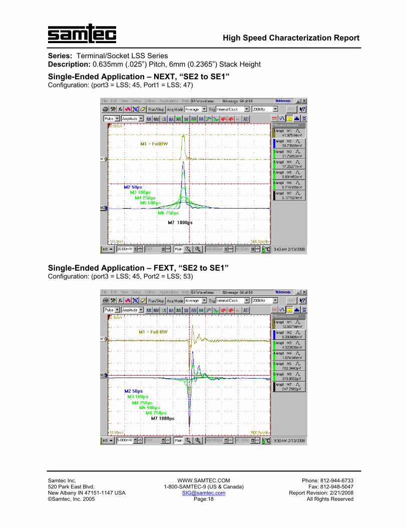
Single-Ended Application – NEXT, “SE2 to SE1” Configuration: (port3 = LSS; 45, Port1 = LSS; 47)
Single-Ended Application – FEXT, “SE2 to SE1” Configuration: (port3 = LSS; 45, Port2 = LSS; 53)

High Speed Characterization Report
Series: Terminal/Socket LSS Series Description: 0.635mm (.025”) Pitch, 6mm (0.2365”) Stack Height
Samtec Inc. WWW.SAMTEC.COM Phone: 812-944-6733 520 Park East Blvd. 1-800-SAMTEC-9 (US & Canada) Fax: 812-948-5047 New Albany IN 47151-1147 USA [email protected] Report Revision: 2/21/2008 ©Samtec, Inc. 2005 Page:19 All Rights Reserved
Single-Ended Application – NEXT, “SE4 to SE3” Configuration: (port3 = LSS; 43, Port1 = LSS; 47)
Single-Ended Application – FEXT, “SE4 to SE3” Configuration: (port3 = LSS; 43, Port2 = LSS; 53)

High Speed Characterization Report
Series: Terminal/Socket LSS Series Description: 0.635mm (.025”) Pitch, 6mm (0.2365”) Stack Height
Samtec Inc. WWW.SAMTEC.COM Phone: 812-944-6733 520 Park East Blvd. 1-800-SAMTEC-9 (US & Canada) Fax: 812-948-5047 New Albany IN 47151-1147 USA [email protected] Report Revision: 2/21/2008 ©Samtec, Inc. 2005 Page:20 All Rights Reserved
Single-Ended Application – NEXT, “SE6 to SE5” Configuration: (port3 = LSS; 4, Port1 = LSS; 3)
Single-Ended Application – FEXT, “SE6 to SE5” Configuration: (port3 = LSS; 4, Port2 = LSS; 97)

High Speed Characterization Report
Series: Terminal/Socket LSS Series Description: 0.635mm (.025”) Pitch, 6mm (0.2365”) Stack Height
Samtec Inc. WWW.SAMTEC.COM Phone: 812-944-6733 520 Park East Blvd. 1-800-SAMTEC-9 (US & Canada) Fax: 812-948-5047 New Albany IN 47151-1147 USA [email protected] Report Revision: 2/21/2008 ©Samtec, Inc. 2005 Page:21 All Rights Reserved
Differential Application – Input Pulse

High Speed Characterization Report
Series: Terminal/Socket LSS Series Description: 0.635mm (.025”) Pitch, 6mm (0.2365”) Stack Height
Samtec Inc. WWW.SAMTEC.COM Phone: 812-944-6733 520 Park East Blvd. 1-800-SAMTEC-9 (US & Canada) Fax: 812-948-5047 New Albany IN 47151-1147 USA [email protected] Report Revision: 2/21/2008 ©Samtec, Inc. 2005 Page:22 All Rights Reserved
Differential Application – Impedance Configuration: port 1=LSS_93-95 port 2=LSS_5-7
Differential Application – Propagation Delay Configuration: port 1=LSS_93-95 port 2=LSS_5-7

High Speed Characterization Report
Series: Terminal/Socket LSS Series Description: 0.635mm (.025”) Pitch, 6mm (0.2365”) Stack Height
Samtec Inc. WWW.SAMTEC.COM Phone: 812-944-6733 520 Park East Blvd. 1-800-SAMTEC-9 (US & Canada) Fax: 812-948-5047 New Albany IN 47151-1147 USA [email protected] Report Revision: 2/21/2008 ©Samtec, Inc. 2005 Page:23 All Rights Reserved
Differential Application – NEXT, “DP2 to DP1” Configuration: (port3 = LSS; 87-89, Port1 = LSS; 91-93)
Differential Application – FEXT, “DP2 to DP1” Configuration: (port3 = LSS; 87-89, Port2 = LSS; 7-9)

High Speed Characterization Report
Series: Terminal/Socket LSS Series Description: 0.635mm (.025”) Pitch, 6mm (0.2365”) Stack Height
Samtec Inc. WWW.SAMTEC.COM Phone: 812-944-6733 520 Park East Blvd. 1-800-SAMTEC-9 (US & Canada) Fax: 812-948-5047 New Albany IN 47151-1147 USA [email protected] Report Revision: 2/21/2008 ©Samtec, Inc. 2005 Page:24 All Rights Reserved
Differential Application – NEXT, “DP4 to DP3” Configuration: (port3 = LSS; 87-89, Port1 = LSS; 93-95)
Differential Application – FEXT, “DP4 to DP3” Configuration: (port3 = LSS; 87-89, Port2 = LSS; 5-7)

High Speed Characterization Report
Series: Terminal/Socket LSS Series Description: 0.635mm (.025”) Pitch, 6mm (0.2365”) Stack Height
Samtec Inc. WWW.SAMTEC.COM Phone: 812-944-6733 520 Park East Blvd. 1-800-SAMTEC-9 (US & Canada) Fax: 812-948-5047 New Albany IN 47151-1147 USA [email protected] Report Revision: 2/21/2008 ©Samtec, Inc. 2005 Page:25 All Rights Reserved
Differential Application – NEXT, “DP6 to DP5” Configuration: (port3 = LSS; 4-6, Port1 = LSS; 3-5)
Differential Application – FEXT, “DP6 to DP5” Configuration: (port3 = LSS; 4-6, Port2 = LSS; 95-97)

High Speed Characterization Report
Series: Terminal/Socket LSS Series Description: 0.635mm (.025”) Pitch, 6mm (0.2365”) Stack Height
Samtec Inc. WWW.SAMTEC.COM Phone: 812-944-6733 520 Park East Blvd. 1-800-SAMTEC-9 (US & Canada) Fax: 812-948-5047 New Albany IN 47151-1147 USA [email protected] Report Revision: 2/21/2008 ©Samtec, Inc. 2005 Page:26 All Rights Reserved
Appendix C – Product and Test System Descriptions Product Description Product samples are the Locking Socket & Terminal Strip LSS Series. Mating connec-tor halves are hermaphroditic and consist of one part number, LSS-150-01-X-DV-A. When mounted to the respective footprint of a PCB a 6mm (0.2755”) stack height exists between boards using a -01/-01 combination. The connectors 150 designation indi-cates the structure consists of two rows of 50 contact terminals mounted into an insulat-ing plastic housing having a PCB surface mount design. Terminals are centerlines on a 0.635mm (0.2362”) pitch. Test System Description The test fixtures are composed of 4-layer FR-4 material with 50Ω and100Ω signal trace and pad configurations designed for the electrical characterization of Samtec hi-speed connector products. The test fixtures are specific to the LSS connector series and iden-tified by Samtec P/N PCB-100993-TST-11, P/N PCB-100993-TST-12, P/N PCB-100993-TST-21 and P/N PCB-100993-TST-22. PCB-100993-TST-11 & PCB-100993-TST-12 serve as the signal launch board and terminate to the specified LSS-01 socket connector product. Test fixtures PCB-100993-TST-21 and P/N PCB-100993-TST-22 terminate to the specified LSS-01 terminal connector product. Electrical continuity ex-ists between labeled test points when PCB-100993-TST-11 mates with PCB-100993-TST-21 and PCB-100993-TST-21 mates with PCB-100993-TST-22. Reference plane and calibration standards specific to the LSS-01/LSS-01 are located on the test calibra-tion board LSS, PCB-100993-TST-99. All data and waveforms presented are results from an LSS-01 side signal launch. Pictured on page 27 are mated 8mm test samples and the panel layout for the breakaway printed circuit boards.

High Speed Characterization Report
Series: Terminal/Socket LSS Series Description: 0.635mm (.025”) Pitch, 6mm (0.2365”) Stack Height
Samtec Inc. WWW.SAMTEC.COM Phone: 812-944-6733 520 Park East Blvd. 1-800-SAMTEC-9 (US & Canada) Fax: 812-948-5047 New Albany IN 47151-1147 USA [email protected] Report Revision: 2/21/2008 ©Samtec, Inc. 2005 Page:27 All Rights Reserved
PCB-100993-TST- Mated 11 & 12, Mated 22 & 23, 6mm Stack Height Test Fixture
PCB-100993-TST PCB Layout Panel

High Speed Characterization Report
Series: Terminal/Socket LSS Series Description: 0.635mm (.025”) Pitch, 6mm (0.2365”) Stack Height
Samtec Inc. WWW.SAMTEC.COM Phone: 812-944-6733 520 Park East Blvd. 1-800-SAMTEC-9 (US & Canada) Fax: 812-948-5047 New Albany IN 47151-1147 USA [email protected] Report Revision: 2/21/2008 ©Samtec, Inc. 2005 Page:28 All Rights Reserved
PCB Fixture Set I Fixture Identity
PCB-100993-TST-11 Rev – LSS Test Board PCB-100993-TST-12 – Rev – LSS Test Board
Crosstalk Test Parameters – TD NEXT, TD NEXT, FD FEXT, TD FEXT, • DP2 to DP1, Differential, GAAVVG, 2:1 Signal to Ground Ratio,
Near-End Aggressor: LSS; 87-89, Victim; LSS, 91-93 Far-End Aggressor: LSS; 87-89, Victim; LSS, 7-9
• SE2 to SE1, Single-Ended, GAVG, 2:1 Signal to Ground Ratio, Near-End Aggressor: LSS; 45, Victim; LSS, 47 Far-End Aggressor: LSS; 45, Victim; LSS, 5
• DP6 to DP5, Differential, GAAG/GVVG, 1:1 Signal to Ground Ratio, Near-End Aggressor: LSS; 4-6, Victim; LSS, 3-5 Far-End Aggressor: LSS; 4-6, Victim; LSS, 95-97
High Speed Characterization Report
Series: Terminal/Socket LSS Series Description: 0.635mm (.025”) Pitch, 6mm (0.2365”) Stack Height
Samtec Inc. WWW.SAMTEC.COM Phone: 812-944-6733 520 Park East Blvd. 1-800-SAMTEC-9 (US & Canada) Fax: 812-948-5047 New Albany IN 47151-1147 USA [email protected] Report Revision: 2/21/2008 ©Samtec, Inc. 2005 Page:29 All Rights Reserved
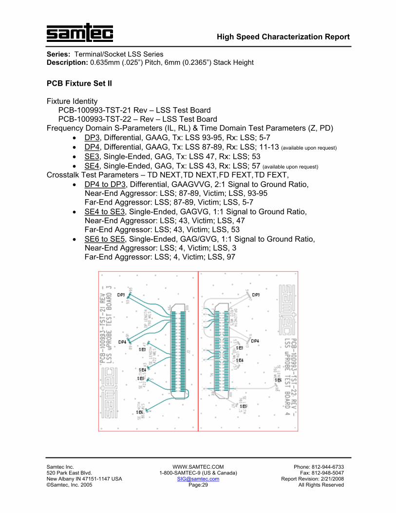
PCB Fixture Set II Fixture Identity
PCB-100993-TST-21 Rev – LSS Test Board PCB-100993-TST-22 – Rev – LSS Test Board
Frequency Domain S-Parameters (IL, RL) & Time Domain Test Parameters (Z, PD) • DP3, Differential, GAAG, Tx: LSS 93-95, Rx: LSS; 5-7 • DP4, Differential, GAAG, Tx: LSS 87-89, Rx: LSS; 11-13 (available upon request) • SE3, Single-Ended, GAG, Tx: LSS 47, Rx: LSS; 53 • SE4, Single-Ended, GAG, Tx: LSS 43, Rx: LSS; 57 (available upon request)
Crosstalk Test Parameters – TD NEXT, TD NEXT, FD FEXT, TD FEXT, • DP4 to DP3, Differential, GAAGVVG, 2:1 Signal to Ground Ratio,
Near-End Aggressor: LSS; 87-89, Victim; LSS, 93-95 Far-End Aggressor: LSS; 87-89, Victim; LSS, 5-7
• SE4 to SE3, Single-Ended, GAGVG, 1:1 Signal to Ground Ratio, Near-End Aggressor: LSS; 43, Victim; LSS, 47 Far-End Aggressor: LSS; 43, Victim; LSS, 53
• SE6 to SE5, Single-Ended, GAG/GVG, 1:1 Signal to Ground Ratio, Near-End Aggressor: LSS; 4, Victim; LSS, 3 Far-End Aggressor: LSS; 4, Victim; LSS, 97

High Speed Characterization Report
Series: Terminal/Socket LSS Series Description: 0.635mm (.025”) Pitch, 6mm (0.2365”) Stack Height
Samtec Inc. WWW.SAMTEC.COM Phone: 812-944-6733 520 Park East Blvd. 1-800-SAMTEC-9 (US & Canada) Fax: 812-948-5047 New Albany IN 47151-1147 USA [email protected] Report Revision: 2/21/2008 ©Samtec, Inc. 2005 Page:30 All Rights Reserved
LSS/LSS Calibration Standards
Propagation Delay Reference Length Standard Differential, 1782 mils Propagation Delay Reference Length Standard Single-Ended, 1182mils TDA Step Waveform Transmission/Reflection Standard

High Speed Characterization Report
Series: Terminal/Socket LSS Series Description: 0.635mm (.025”) Pitch, 6mm (0.2365”) Stack Height
Samtec Inc. WWW.SAMTEC.COM Phone: 812-944-6733 520 Park East Blvd. 1-800-SAMTEC-9 (US & Canada) Fax: 812-948-5047 New Albany IN 47151-1147 USA [email protected] Report Revision: 2/21/2008 ©Samtec, Inc. 2005 Page:31 All Rights Reserved
Appendix D – Test and Measurement Setup The test instrument is the Tektronix CSA8000 Communication Signal Analyzer Main-frame. Four bays of the CSA8000 use four Tektronix 80E04 TDR/Sampling Heads. Time domain data and graphs are real-time. Post-processed s-parameter data and graphs extend from a TDR based software tool called I-Connect Probing uses a video microscopy system, microprobe positioners, and 40GHz capable probes. Four hundred and fifty micron pitch probes are located to PCB launch points with 25X to 175X magni-fication and XYZ fine positioning adjustments available from both the probe table and micro-probe positioners. Electrically the microwave probes rate a < 1.0 dB insertion loss, a ≥18 dB return loss, and an isolation of 38 dB providing high-bandwidth and low parasitic measurement results. Combined, the above technology provides a stable measurement environment along with the electrical accuracies for obtaining precise calibrations and signal launch capabilities CSA8000/TDA IConnect Measurements Capability

High Speed Characterization Report
Series: Terminal/Socket LSS Series Description: 0.635mm (.025”) Pitch, 6mm (0.2365”) Stack Height
Samtec Inc. WWW.SAMTEC.COM Phone: 812-944-6733 520 Park East Blvd. 1-800-SAMTEC-9 (US & Canada) Fax: 812-948-5047 New Albany IN 47151-1147 USA [email protected] Report Revision: 2/21/2008 ©Samtec, Inc. 2005 Page:32 All Rights Reserved
Four Position Dual 40 GHz Microprobe Setup
Test Instruments QTY Description
1 Tektronix CSA8000 Communication Signal Analyzer 4 Tektronix 80E04 Dual Channel 20 GHz TDR Sampling Module 1 Tektronix 80E03 Dual Channel 20 GHz Sampling Module
Measurement Station Accessories QTY Description
1 GigaTest Labs Model (GTL3030) Probe Station 4 GTL Micro-Probe Positioners 4 Picoprobe by GGB Ind. Dual Model 40A GSG-GSG (differential applications) 1 Keyence VH-5910 High Resolution Video Microscope 1 Keyence VH-W100 Fixed Magnification Lens 100 X 1 Keyence VH-Z25 Standard Zoom Lens 25X-175X
Test Cables & Adapters QTY Description
8 Pasternack Enterprises 2.9mm Semi-Rigid (.086) 9” Cable Assemblies 4 Tektronix 1 Meter Module Extenders
High Speed Characterization Report
Series: Terminal/Socket LSS Series Description: 0.635mm (.025”) Pitch, 6mm (0.2365”) Stack Height
Samtec Inc. WWW.SAMTEC.COM Phone: 812-944-6733 520 Park East Blvd. 1-800-SAMTEC-9 (US & Canada) Fax: 812-948-5047 New Albany IN 47151-1147 USA [email protected] Report Revision: 2/21/2008 ©Samtec, Inc. 2005 Page:33 All Rights Reserved
Appendix E - Frequency and Time Domain Measurements It is important to note before gathering measurement data that TDA Systems IConnect measurements and CSA8000 measurements are virtually the same measurements with diverse formats. This means that the operator, being extremely aware, can obtain SI time and frequency characteristics in an almost simultaneous fashion. Since IConnect setup procedures are specific to the frequency information sought, it is mandatory that the sample preparation and CSA8000 functional setups be consistent throughout the waveform gathering process. If the operators test equipment permits recall sequencing between the various test parameter setups, it insures IConnect func-tional setups remain consistent with the TDR/TDT waveforms previously recorded. Sample Preparation Determine signal launch and monitoring test points by referencing the pin-out maps Calibration Board, CAL PCB Fixture Sets I & II It is a good practice to terminate all non-active signal lines immediately adjacent to the designated active or quiet signal lines under test. Frequency (S-Parameter) Domain Procedures Frequency data extraction involves a two-step process. The first step creates the TDR based waveform relationships utilizing a Tektronix CSA8000 time based instrument. The second step involves the conversion of these time-based waveforms into s-parameter format using the TDA Systems IConnect software tool. TDA Systems labels time related conversion waveforms as the Step and DUT waveform references. This section establishes the setup procedures for defining the Step and DUT reference for conversion to frequency s-parameters presented in this report. CSA8000 Setup Listed below is the CSA 8000 functional menu setups used for single-ended and differ-ential frequency response extractions. Both signal types utilize I-Connect software tools to generate S-parameter upper and lower frequency boundaries along with the step fre-quency. Functional settings such as window length, number of points and averaging capability determines the instruments frequency boundaries. Once window length, number of points and averaging functions are set, maintain the same instrument set-tings throughout the extraction process. The single channel pulsed source processes s-parameters in single-ended format. A dual channel differential pulsed source proc-esses s-parameters in differential format.

High Speed Characterization Report
Series: Terminal/Socket LSS Series Description: 0.635mm (.025”) Pitch, 6mm (0.2365”) Stack Height
Samtec Inc. WWW.SAMTEC.COM Phone: 812-944-6733 520 Park East Blvd. 1-800-SAMTEC-9 (US & Canada) Fax: 812-948-5047 New Albany IN 47151-1147 USA [email protected] Report Revision: 2/21/2008 ©Samtec, Inc. 2005 Page:34 All Rights Reserved
Single-Ended Signal Differential Signal Vertical Scale: 100 mV/ Div: 100 mV/ Div: Offset: Default / Scroll Default / Scroll Horizontal Scale: 1nSec/ Div = 20 MHz step
frequency 1nSec/ Div = 20 MHz step frequency
Max. Record Length: 4000 = Min. Resolution 4000 = Min. Resolution Averages: ≥ 128 ≥ 128 Insertion Loss (TDA conversion) Step Waveform - determine TD waveform by making a TDT transmission measure-ment that includes all cables, adapters, and probes connected in the test systems transmission path. Complete the transmission path by inserting a negligible length of transmission standard between the system test probes. Calibration or waveform refer-encing utilizes a six pad cal structure for each of the probe touchdowns (ie; se thru = 3 pads or diff thru = 6 pads). Reference the calibration board CAL, and use the 1mm (0.390”) length calibration reflect/transmission structure for TDA step waveform charac-terization. DUT Waveform - determine TD waveform by making an active TDT transmission measurement that includes all cables, adapters, and probes connected in the test sys-tems transmission path. Insert the SUT between the probes in place of the reflec-tion/transmission standard and record the measurement. The LSS-01/LSS-01 charac-terization reports one single-ended and one differential insertion loss application. Sin-gle-ended and differential line measurement possibilities are SE3, SE4 DP3 and DP4. Reference PCB fixture set II for the configured signal path. Return Loss (TDA conversion) Step Waveform – determine TD waveform by making an active TDR reflection meas-urement that includes all cables, adapters, and probes connected in the test systems electrical path up to and including an open standard. Calibration or waveform referenc-ing utilizes three pads for each probe touchdown (ie; se reflect = 3 pads or diff reflect = 6 pads). Reference the calibration board CAL, and use the 1mm (0.390”) length calibra-tion reflect/transmission structure for TDA step waveform characterization. DUT Waveform – determine waveform by making an active TDR reflection measure-ment that includes all cables, adapters, and probes connected in the test systems transmission path. Insert the SUT between the probes in place of the reflec-tion/transmission standard and record the measurement. In this condition cables and

High Speed Characterization Report
Series: Terminal/Socket LSS Series Description: 0.635mm (.025”) Pitch, 6mm (0.2365”) Stack Height
Samtec Inc. WWW.SAMTEC.COM Phone: 812-944-6733 520 Park East Blvd. 1-800-SAMTEC-9 (US & Canada) Fax: 812-948-5047 New Albany IN 47151-1147 USA [email protected] Report Revision: 2/21/2008 ©Samtec, Inc. 2005 Page:35 All Rights Reserved
adapters located at the far-end of the inserted SUT function as the systems 50Ω single-ended and/or 100Ω differential matching impedance. The LSS-01/LSS-01 characteriza-tion reports one single-ended and one differential return loss application. Single-ended and differential line measurement possibilities are SE3 & SE4, and DP3 & DP4. Refer-ence PCB fixture set II for the configured signal path. Near-End Crosstalk (TDA conversion) Step Waveform – Use Return Loss (RL) step waveform. DUT Waveform - determine waveform by driving specified signal type and monitoring coupled energy levels at the configurations adjacent near-end signal line. LSS-01/LSS-01 examines three single-ended and three differential near-end XT configurations. Sin-gle-ended crosstalk measurements are SE2 to SE1, SE4 to SE3, and SE6 to SE5. Dif-ferential crosstalk measurements are DP2 to DP1, DP4 to DP3, and DP6 to DP5. Ref-erence both PCB fixture set I and fixture set II for crosstalk configurations. Far-End Crosstalk (TDA conversion) Step Waveform - Use Insertion Loss (IL) step waveform. DUT Waveform - determine waveform by driving specified signal type and monitoring coupled energy levels at the configurations adjacent far-end signal line. LSS-01/LSS-01 examines three single-ended and three differential far-end XT configurations. Single-ended crosstalk measurements are SE2 to SE1, SE4 to SE3, and SE6 to SE5. Differ-ential crosstalk measurements are DP2 to DP1, DP4 to DP3, and DP6 to DP5. Refer-ence both PCB fixture set I and fixture set II for crosstalk configurations.

High Speed Characterization Report
Series: Terminal/Socket LSS Series Description: 0.635mm (.025”) Pitch, 6mm (0.2365”) Stack Height
Samtec Inc. WWW.SAMTEC.COM Phone: 812-944-6733 520 Park East Blvd. 1-800-SAMTEC-9 (US & Canada) Fax: 812-948-5047 New Albany IN 47151-1147 USA [email protected] Report Revision: 2/21/2008 ©Samtec, Inc. 2005 Page:36 All Rights Reserved
Time Domain Procedures Utilize the Time Domain Reflectometer (TDR) or Time Domain Transmission (TDT) method for digital type pulse measurements. Impedance and propagation delay charac-terization utilize TDR measurement methods. Crosstalk measurements utilize TDT methods. The Tektronix 80E04 TDR/ Sampling Head provide both the signaling type and sampling capability necessary to characterize the SUT. Impedance(TDR) Energize the SUT’s signal line(s) with a TDR pulse. The far-end of the energized signal lines are terminated in the test systems characteristic impedance (e.g.; 50Ω or 100Ω termination) or use quality cables and adapters located at the far-end of the inserted SUT function as the systems 50Ω single-ended and/or 100Ω differential matching im-pedance. The LSS-01/LSS-01 characterization reports one single-ended and one differ-ential impedance application. Single-ended and differential line measurement possibili-ties are SE3, SE4, DP3, and DP4. Reference PCB fixture set II for a configured signal path. Propagation Delay (TDT) This test reports differential or single ended signal delay as the measured difference of propagation between a combined electrical length of the input/output signal pads and traces (35 ± 5 ps edge rate) and the device under test (DUT) plus a referenced electri-cal length of the signal pads and signal traces (PDpads/traces- PDDUT + PDpads/traces). The recorded delay is the signal delay of the connector only. PDpads/traces is the nomencla-ture representing the electrical length of PCB signal pads & traces equal to physical lengths of PCB pads & traces entering and leaving the device under test (DUT). The PDDUT + PDpads/traces variable is the mated DUT fixture. Measure the risetime of PDpads/traces waveform & PDDUT + PDpads/traces waveforms. Record the 50% amplitude of each rising edge. The distance in time between the rising edges is the propagation de-lay of the device under test (DUT). Single-ended and differential line measurement pos-sibilities are SE3, SE4, DP3, and DP4. Reference the calibration board CAL for in-put/output signal line traces and PCB fixture set II for a configured signal path. . Near-End Crosstalk (TDT) Energize the pre-determined signal line(s) with the appropriate signal type. Monitor the configurations adjacent quiet signal line at the near-end for magnitudes of coupled en-ergy. Terminate adjacent signal lines not under test into the test systems characteristic impedance. LSS-01/LSS-01 examines three single-ended and three differential near-end XT configurations. Single-ended crosstalk measurements are SE2 to SE1, SE4 to SE3, and SE6 to SE5. Differential crosstalk measurements are DP2 to DP1, DP4 to DP3, and DP6 to DP5. Reference both PCB fixture set I and fixture set II for crosstalk configurations.

High Speed Characterization Report
Series: Terminal/Socket LSS Series Description: 0.635mm (.025”) Pitch, 6mm (0.2365”) Stack Height
Samtec Inc. WWW.SAMTEC.COM Phone: 812-944-6733 520 Park East Blvd. 1-800-SAMTEC-9 (US & Canada) Fax: 812-948-5047 New Albany IN 47151-1147 USA [email protected] Report Revision: 2/21/2008 ©Samtec, Inc. 2005 Page:37 All Rights Reserved
Far-End Crosstalk (TD) Energize the pre-determined signal line(s) with the appropriate signal type. Monitor the configurations adjacent quiet signal line at the far-end for magnitudes of coupled en-ergy. Terminate adjacent signal lines not under test into the test systems characteristic impedance. LSS-01/LSS-01 examines three single-ended and three differential far-end XT configurations. Single-ended crosstalk measurements are SE2 to SE1, SE4 to SE3, and SE6 to SE5. Differential crosstalk measurements are DP2 to DP1, DP4 to DP3, and DP6 to DP5. Reference both PCB fixture set I and fixture set II for crosstalk con-figurations.

High Speed Characterization Report
Series: Terminal/Socket LSS Series Description: 0.635mm (.025”) Pitch, 6mm (0.2365”) Stack Height
Samtec Inc. WWW.SAMTEC.COM Phone: 812-944-6733 520 Park East Blvd. 1-800-SAMTEC-9 (US & Canada) Fax: 812-948-5047 New Albany IN 47151-1147 USA [email protected] Report Revision: 2/21/2008 ©Samtec, Inc. 2005 Page:38 All Rights Reserved
Appendix F – Glossary of Terms TD – Time Domain FD – Frequency domain DUT – Device under test, term used for TDA IConnect & Propagation Delay waveforms EC6 – Edge Card with a .635mm signal pad pitch FEXT – Far-End Crosstalk GSG – Ground–Signal-Ground; geometric configuration GSSG - Ground–Signal-Signal-Ground; geometric configuration LEC6 – Signal Launch Edge Card with a .635 mm signal pad pitch NEXT – Near-End Crosstalk PCB – Printed Circuit Board SE – Single-Ended SI – Signal Integrity SUT – System Under Test TDR – Time Domain Reflectometry TDT – Time Domain Transmission WC – Worst Case crosstalk configuration BC – Best Case crosstalk configuration Z – Impedance (expressed in ohms) OV – Optimal Vertical OH – Optimal Horizontal HDV – High Density Vertical PPO – Pin Population Option S – Static (independent of PCB ground)
Related Documents


