Journal of Microscopy, Vol. 00, Issue 0 2015, pp. 1–7 doi: 10.1111/jmi.12224 Received 12 September 2014; accepted 23 December 2014 High-resolution, high-throughput imaging with a multibeam scanning electron microscope A.L. EBERLE ∗ , S. MIKULA †, R. SCHALEK ‡, J.W. LICHTMAN ‡, M.L. KNOTHE TATE§ & D. ZEIDLER ∗ ∗ Carl Zeiss Microscopy GmbH, Oberkochen, Germany †Max-Planck-Institute for Medical Research, Heidelberg, Germany ‡Department of Molecular and Cell Biology, Harvard University, Cambridge, Massachusetts, U.S.A §Graduate School of Biomedical Engineering, University of New South Wales, Sydney, Australia Key words. High-throughput imaging, multibeam, parallel data acquisition, scanning electron microscopy. Summary Electron–electron interactions and detector bandwidth limit the maximal imaging speed of single-beam scanning electron microscopes. We use multiple electron beams in a single col- umn and detect secondary electrons in parallel to increase the imaging speed by close to two orders of magnitude and demon- strate imaging for a variety of samples ranging from biological brain tissue to semiconductor wafers. Introduction Electron microscopy is commonly used to image biologi- cal samples, enabling acquisition of high-resolution images from small sample regions, typically in the range of several micrometres. However, there is an increasing need for large area imaging or even volume imaging of biological tissues at nanoscopic resolution comprising billions of pixels. An exam- ple is connectomics, an emerging field in neuroscience aimed at comprehensively reconstructing neural circuits (Lichtman & Denk, 2011; Helmst¨ adter et al., 2013) and analysing ex- tended cellular structures (Holcomb et al., 2013). To image surfaces, such as in the serial block-face technique (Denk & Horstmann, 2004) or with ultrathin sections on a solid substrate (Micheva & Smith, 2007; Horstmann et al., 2012), scanning electron microscopes (SEMs) need to be used, which conventionally acquire an image one pixel at a time. This lim- its the data acquisition rate and, in turn, the sample size that can be imaged within a reasonable amount of time. As an ex- ample, mapping a 1 mm cube of tissue with an isotropic voxel size of 4 nm will result in almost 16 petabytes of data. Data acquisition at 20 MHz would require a total acquisition time Correspondence to: Anna Lena Eberle, Carl Zeiss Microscopy GmbH, Carl-Zeiss-Str. 22, D-73447 Oberkochen, Germany. Tel: +49 7364 20 6853; fax: +49 7364 20 9456; e-mail: [email protected] of almost 25 years, even before taking into account overhead times such as those due to stage movements. Another application is quality control, such as is needed for wafer production, where we need to detect nanometre-sized particles and defects (Patterson et al., 2012). A similar proto- col is followed in medical research where histological samples are searched for characteristic motifs, antibodies or nanoparti- cles (Kaiser et al., 2013). Due to throughput limitations, these methods are confined to analyses of a small fraction of the sam- ple surface, thereby increasing the number of ‘false negative’ events. Finally, organs and tissues exhibit architectures which emerge hierarchically from cell-scale events culminating at the macroscale and resulting in ‘smart’ or stimuli-responsive properties (Evans et al., 2013). Application of experiments and computer models in parallel enables mechanistic elucidation of these system properties (Knothe Tate, 2011; Moore et al., 2014). To date, different imaging methods had to be used to bridge the gap between different length scales. The capability to image the structure of organs and tissues seamlessly across length scales using high-throughput electron microscopy is expected to facilitate understanding of functional implica- tions across length scales. The above-mentioned applications show that there is a strong need for high-throughput electron microscopy that can image large areas or volumes at high resolution. However, be- cause scanning electron microscopy is widely thought of as an inherently low-throughput technique, the SEM may not even be considered for applications that require high-throughput imaging. Here, we demonstrate a multibeam SEM with a throughput increase by almost two orders of magnitude. Throughput limitations of single-beam SEMs The signal-to-noise ratio in an SEM image depends on beam current, pixel dwell time, sample contrast and detection C 2015 The Authors Journal of Microscopy C 2015 Royal Microscopical Society

Welcome message from author
This document is posted to help you gain knowledge. Please leave a comment to let me know what you think about it! Share it to your friends and learn new things together.
Transcript
Journal of Microscopy, Vol. 00, Issue 0 2015, pp. 1–7 doi: 10.1111/jmi.12224
Received 12 September 2014; accepted 23 December 2014
High-resolution, high-throughput imaging with a multibeamscanning electron microscope
A . L . E B E R L E ∗, S . M I K U L A†, R . S C H A L E K‡, J . W . L I C H T M A N‡, M . L . K N O T H E T A T E § & D . Z E I D L E R ∗∗Carl Zeiss Microscopy GmbH, Oberkochen, Germany
†Max-Planck-Institute for Medical Research, Heidelberg, Germany
‡Department of Molecular and Cell Biology, Harvard University, Cambridge, Massachusetts, U.S.A
§Graduate School of Biomedical Engineering, University of New South Wales, Sydney, Australia
Key words. High-throughput imaging, multibeam, parallel data acquisition,scanning electron microscopy.
Summary
Electron–electron interactions and detector bandwidth limitthe maximal imaging speed of single-beam scanning electronmicroscopes. We use multiple electron beams in a single col-umn and detect secondary electrons in parallel to increase theimaging speed by close to two orders of magnitude and demon-strate imaging for a variety of samples ranging from biologicalbrain tissue to semiconductor wafers.
Introduction
Electron microscopy is commonly used to image biologi-cal samples, enabling acquisition of high-resolution imagesfrom small sample regions, typically in the range of severalmicrometres. However, there is an increasing need for largearea imaging or even volume imaging of biological tissues atnanoscopic resolution comprising billions of pixels. An exam-ple is connectomics, an emerging field in neuroscience aimedat comprehensively reconstructing neural circuits (Lichtman& Denk, 2011; Helmstadter et al., 2013) and analysing ex-tended cellular structures (Holcomb et al., 2013). To imagesurfaces, such as in the serial block-face technique (Denk& Horstmann, 2004) or with ultrathin sections on a solidsubstrate (Micheva & Smith, 2007; Horstmann et al., 2012),scanning electron microscopes (SEMs) need to be used, whichconventionally acquire an image one pixel at a time. This lim-its the data acquisition rate and, in turn, the sample size thatcan be imaged within a reasonable amount of time. As an ex-ample, mapping a 1 mm cube of tissue with an isotropic voxelsize of 4 nm will result in almost 16 petabytes of data. Dataacquisition at 20 MHz would require a total acquisition time
Correspondence to: Anna Lena Eberle, Carl Zeiss Microscopy GmbH, Carl-Zeiss-Str.
22, D-73447 Oberkochen, Germany. Tel: +49 7364 20 6853; fax: +49 7364 20
9456; e-mail: [email protected]
of almost 25 years, even before taking into account overheadtimes such as those due to stage movements.
Another application is quality control, such as is needed forwafer production, where we need to detect nanometre-sizedparticles and defects (Patterson et al., 2012). A similar proto-col is followed in medical research where histological samplesare searched for characteristic motifs, antibodies or nanoparti-cles (Kaiser et al., 2013). Due to throughput limitations, thesemethods are confined to analyses of a small fraction of the sam-ple surface, thereby increasing the number of ‘false negative’events.
Finally, organs and tissues exhibit architectures whichemerge hierarchically from cell-scale events culminating atthe macroscale and resulting in ‘smart’ or stimuli-responsiveproperties (Evans et al., 2013). Application of experiments andcomputer models in parallel enables mechanistic elucidationof these system properties (Knothe Tate, 2011; Moore et al.,2014). To date, different imaging methods had to be used tobridge the gap between different length scales. The capabilityto image the structure of organs and tissues seamlessly acrosslength scales using high-throughput electron microscopyis expected to facilitate understanding of functional implica-tions across length scales.
The above-mentioned applications show that there is astrong need for high-throughput electron microscopy that canimage large areas or volumes at high resolution. However, be-cause scanning electron microscopy is widely thought of as aninherently low-throughput technique, the SEM may not evenbe considered for applications that require high-throughputimaging. Here, we demonstrate a multibeam SEM with athroughput increase by almost two orders of magnitude.
Throughput limitations of single-beam SEMs
The signal-to-noise ratio in an SEM image depends on beamcurrent, pixel dwell time, sample contrast and detection
C© 2015 The AuthorsJournal of Microscopy C© 2015 Royal Microscopical Society

2 A . L . E B E R L E E T A L .
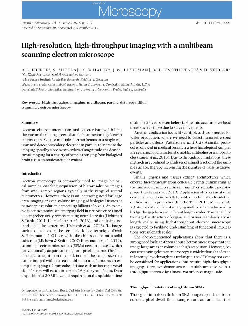
Fig. 1. The multibeam SEM uses multiple beams in parallel to image a hexagonal sample area 100-µm wide. Primary electrons (solid lines, left) arefocused onto the specimen and separated by a beam splitter from the secondary electrons (dotted lines, right) which are detected simultaneously. Allelectron beams form many individual images which are then merged into a single, large area micrograph.
efficiency. It has to be larger than a minimum signal-to-noise ratio to make features in the data set – the signal –visible sufficiently well against background noise (Bright etal. 1998). If we want to increase throughput by decreas-ing the pixel dwell time, we have to increase the beam cur-rent to maintain the signal-to-noise ratio if all other param-eters remain unchanged. Increasing the beam current willlead to increasing Coulomb interactions between the elec-trons, thereby blurring the electron beam and reducing theresolution. Moreover, we cannot operate electron detectorsfaithfully at arbitrarily high rates because electrons of dif-ferent energies reach the detector at different times, therebylimiting the effective detector bandwidth. Another limitationof the bandwidth of efficient secondary electron (SE) detec-tors is determined by signal decay time, such as occurs at ascintillator.
Circumventing the single-beam limitations with a multibeamapproach
The multibeam SEM currently uses 61 electron beams ina single column and one dedicated detector for each beamto alleviate Coulomb interaction limitations and bypass thedetector bandwidth limit. The principle of operation is depicted
in Figure 1: A multiple beam electron source produces a reg-ular array of electron beams that are imaged onto the sample,forming a pattern of 61 primary electron foci. The array ofprimary beams is arranged in a hexagonal pattern to minimizeelectron optical aberrations. The SEs that emanate from eachprimary electron spot are imaged onto a multidetector withone detection unit for each electron beam. A magnetic sectorfield separates primary electron and SE beams. The electronbeams are scanned over the sample, and the SE signal isrecorded for each scan position as in conventional SEMs.One single scanning pass thus produces multiple imagesin parallel yielding a complete image of the sample regionunderneath the primary beam array. A number of options forproducing an array of electron beams has been demonstrated(Platzgummer et al., 2013 and references therein). Moreoptions to perform imaging with a multibeam electron micro-scope have also been demonstrated (Mohammadi-Gheidariet al., 2010; Mohammadi-Gheidari & Kruit, 2011; Enyamaet al., 2014).
The total possible detector bandwidth of the multibeam SEMis the single detector bandwidth times the number of beams, inthis case 1.22 GPixel/s. The Coulomb interaction is lower thanin a single-beam configuration, as the charge is distributedacross many beams and therefore spread over a larger volume
C© 2015 The AuthorsJournal of Microscopy C© 2015 Royal Microscopical Society, 00, 1–7

H I G H - T H R O U G H P U T I M A G I N G W I T H A M U L T I B E A M S E M 3
Fig. 2. Cerebral cortex of mouse brain (block-face), sample by Winfried Denk and Shawn Mikula, Max Planck Society, showing unmyelinated neuronaland glial processes and a neuronal nucleus (left of centre), acquired by the multibeam SEM at 0.45 GPixel/s and 3.8 nm pixel size, 26 nA total current,270 electrons per pixel, scale bar: 10 µm. A 1–2 nm coat of palladium has been evaporated onto the block-face to dissipate charging (Titze & Denk,2013). Within the cellular processes, mitochondria, microtubules, synapses and endoplasmic reticulum are visible. Inset lower right: 12 µm × 10 µmsingle-beam subimage, detail of the full multibeam image, scale bar: 5 µm.
inside the electron optical column. The data acquisition com-puter system is highly parallelized to accommodate the largedata acquisition rates and enable comparably low-bandwidthstorage solutions.
Application examples of the multibeam SEM
We demonstrate that the speed increase is achieved with anumber of samples from the above-mentioned applicationsand that the multibeam SEM is compatible with the corre-sponding sample preparation methods. Typical landing ener-gies of the multibeam electron microscope are 1–3 keV, typicalpixel sizes are 4–10 nm. The electron optical setup has beenchosen such that the distance between single beams is 12µm.The number of pixels per image in x and y and the pixel size areindependent of the beam distance and have been chosen suchthat a small overlap between the images is obtained, whichrequires an aspect ratio of about 0.866 between x and y. Inprinciple, other pixel sizes and aspect ratios can be chosen, butmight result in too large overlaps or no overlap at all. In thefollowing examples, the 61 images have been merged into one
large image that contains up to 500 MPixel over a hexagonalarea approximately 100 µm wide.
For the large-volume investigation of biological tissues, anexample is the volumetric reconstruction of a macroscopicvolume of mouse brain tissue (Lichtman & Denk, 2011). Toobtain such data, a number of solutions for sectioning andimaging exist (Briggman & Bock, 2012). For example, a sliceof several nanometres in thickness can be removed from thesample surface using an in-chamber microtome. The freshlyexposed sample surface is then imaged with an SEM. Repeat-ing this process many times yields a data set of the entire vol-ume (Denk & Horstmann, 2004). It is also possible to collectultrathin sections on a flat substrate and subsequently im-age them with an SEM (Micheva & Smith, 2007; Horstmannet al., 2012). The multibeam SEM is compatible with bothmethods, as demonstrated in Figures 2 and 3. Figure 2 showsa subregion from a coronal block-face of an osmium-stainedmouse brain (Mikula et al., 2012; Mikula & Denk, 2014,in preparation) taken at approximately Bregma 1.5 mm.Figure 3 shows a multibeam SEM acquisition from a serialsection taken from an osmium-stained mouse brain block.
C© 2015 The AuthorsJournal of Microscopy C© 2015 Royal Microscopical Society, 00, 1–7

4 A . L . E B E R L E E T A L .
Fig. 3. Cortex of mouse brain (serial ultrathin section), sample by Jeff Lichtman and Richard Schalek, Harvard University, showing myelinated axons,plasma membranes, cell somata and dendrites, acquired by the multibeam SEM at 0.45 GPixel/s and 3.8 nm pixel size, 26 nA total current, 270 electronsper pixel, scale bar: 10 µm. Sample charging has been mitigated by placing the thin sections on a conductive surface such that no additional conductivecoating is required. Within the cells, dendrites and axons, organelles such as mitochondria and endoplasmic reticulum are visible. Inset lower right:12 µm × 10 µm single-beam subimage, detail of the full multibeam image, scale bar: 5 µm. Inset upper right: 3 µm × 2.6 µm detail of the single-beamsubimage, scale bar: 1µm.
The sample preparation with an automatic section collectiondevice has been described in Hayworth et al. (2006) and Tapiaet al. (2012). The whole experimental setup is designed suchthat a high degree of automation enables the reliable acqui-sition of large quantities of EM data (Hayworth et al., 2014).We expect the signal in Figures 2 and 3 to be composed ofSE1 and SE2 electrons mainly (Reimer, 1993; Cazaux, 2004)with a penetration depth of the SE1 contribution of about10–20 nm (Seiler, 1983) and a slightly higher penetrationdepth for the SE2 contributions (Hennig & Denk, 2007). TheSE1 contributions are known to be dependent on surface topol-ogy (Griffin, 2011), such as knife marks and section folds.These defects are addressed by optimizing the sample prepara-tion such that the frequency of occurrence is minimized andby data postprocessing.
Imaging tissues or organs over several length scales resultsin samples of up to several centimetres diameter. Sample prepa-ration requires special attention to provide a sufficiently uni-form sample fixation and surface smoothness. Figure 4 showsthe multibeam SEM image of a section of a human femoralneck collected per IRB (institutional review board) protocol
guidelines, and normally discarded in the course of hip re-placement surgery (Chang et al., 2014). Tissues are sectionedand prepared for undecalcified histology with bulk embed-ding in polymethylmethacrylate. After curing of the resin, thesurface is trimmed and smoothed for SEM inspection of theblock-face (Knothe Tate, 2015, in preparation).
All composite images (Figs. 2–5) show sufficient contrastin all subimages and the resolution of all subimages varies byonly a few percent. The crosstalk between adjacent beams isbelow 1%. To make the imaging capabilities of the multibeamSEM accessible to large-scale applications, it is desirable toautomate the data acquisition process.
Operating a multibeam SEM
Because the fundamental principles of an SEM are conservedin the multibeam SEM, operation is in many respects identicalto operating a single-beam SEM. The main difference is that amultibeam SEM requires a higher degree of automation duringadjustment, such as measuring and controlling parameters
C© 2015 The AuthorsJournal of Microscopy C© 2015 Royal Microscopical Society, 00, 1–7

H I G H - T H R O U G H P U T I M A G I N G W I T H A M U L T I B E A M S E M 5
Fig. 4. Femoral neck (PMMA-embedded and polished block-face), sample by Melissa Knothe Tate, University of New South Wales, and Ulf Knothe,Cleveland Clinic, showing an osteon comprising a bone capillary surrounded concentrically by osteocytes, acquired by the multibeam SEM at0.18 GPixel/s and 11.3 nm pixel size, 40 nA total current, 420 electrons per pixel, scale bar: 10 µm. Inset lower right: 12 µm × 10 µm single-beam subimage, detail of the full multibeam image, showing one osteocyte, scale bar: 5 µm.
(e.g. focus, stigmation, relative beam position) for all beams,which is difficult and time consuming for a human operator.As an example, the illumination optics of a multibeam SEMtypically consist of a number of electron optical lenses. Duringgeneral alignment, if focus adjustment is needed, changing theexcitation of one of the lenses results not only in the changeof focus, but also in a change of beam pitch at the sample. Ifthe excitation of a magnetic lens is changed, not only will thebeam pitch be altered, but also the rotation of the beam posi-tions around the central beam. Thus, adjusting one parametersuch as focus requires that multiple lens settings must be ad-justed accordingly. This is most conveniently solved by analgorithm in connection with an appropriate test sample. Onepossible test sample is shown in Figure 5. It contains test struc-tures written onto a wafer, which are suitable for automatedalignment and calibration of a multibeam SEM. During dataacquisition, for very small changes of focus (and stigmation),using just one lens (or stigmator) for automatic alignment isusually sufficient, and may be performed fast on any type ofsample with sufficient structural information. The frequencyof the automatic alignment depends on sample properties suchas sample flatness, as the drifts of the multibeam SEM are small.
Furthermore, as large data sets are automatically acquiredand evaluated by algorithms, many images are likely to never
be inspected by a human being. Therefore, a large degreeof automation is required during the data acquisition pro-cess as well. We will demonstrate this at the example ofwafer stage movements for seamless acquisition of samplesurfaces.
Acquiring large areas with a multibeam SEM is performedin the same manner as with a single-beam SEM: The sam-ple is mounted onto a stage such that multiple fields of view(FoV) cover the areas to be imaged. With a single-beam SEM,an efficient tessellation of the region of interest is possible forany rotation of the SEM scan direction, that is, orientationof the FoV of the single beam, as the movement of the sam-ple can be chosen such that the area is completely coveredwith only small overlaps of the FoV being required. With amultibeam SEM, the tessellation has to take into account therelative beam positions of the multiple beams at the surfaceof the sample. This produces two constraints: (i) In order toproduce an efficient tiling of the sample surface, the directionof the scan rotation of the scanning system that defines theaxes of all single images has to coincide with the directionof one beam to one of its (four or six) nearest neighbours. Indoing so, the FoV for each beam can be chosen equal to thebeam pitch and thus be minimized. If the scan differs from thisbeam orientation, a larger FoV at the same beam pitch must be
C© 2015 The AuthorsJournal of Microscopy C© 2015 Royal Microscopical Society, 00, 1–7

6 A . L . E B E R L E E T A L .
Fig. 5. Test chip showing a hexagonal arrangement of calibration structures for tool adjustments. The structures are printed in an e-beam direct writelithography process with a high placement precision, etched in SiO2 on a Si-substrate, and finally coated with a completely conductive layer, scale bar:10 µm. Pixel size was 3.8 nm, acquisition speed 0.72 GPixel/s, 40 nA total current, 210 electrons per pixel. Inset lower right: 12 µm × 10 µm single-beamsubimage, detail of the full multibeam image, scale bar: 5 µm.
chosen to completely image the area of interest, which meansthat a certain fraction of the surface is scanned more thanonce, leading to a reduction of throughput. Setting the optimalrelation between the two directions is possible by either choos-ing a scan rotation according to the beam positions at thesample, or, if a special scan rotation is desired, by rotating thebeam positions accordingly. The overlap between adjacentsingle-beam images ensures proper stitching of the images tobelow a few pixels within one hexagonal field of view. (ii) Thetessellation of the region to be scanned has to take into accountthe arrangement of beams at the sample surface. For exam-ple, a hexagonal beam arrangement produces a hexagonal-like shaped total FoV for the entirety of all beams. A completetiling of the surface with minimal overlap is then possible usingadapted stage positions. As before, fulfilling these constraintsis most conveniently solved by an algorithm.
Conclusions
We have shown that the multibeam SEM is capable of high-throughput imaging (approaching 1 GHz) of a variety of sam-ples of different compositions and contrast mechanisms, lead-
ing to a remarkable reduction in image acquisition time com-pared to a conventional single-beam SEM. Thus, we expectthat the multibeam SEM will open up new fields of researchwhere nanometre-resolution imaging over macroscopic areasand volumes in the range from millimetre to centimetre (Marx,2013) are of utmost importance.
Acknowledgements
The authors thank Winfried Denk for providing data for thiswork and scientific advice, Tomasz Garbowski for the prepa-ration of the images and Ingo Muller, Stephan Nickell, PascalAnger and Gregor Dellemann for discussions.
References
Briggman, K.L. & Bock, D. (2012) Volume electron microscopy for neu-ronal circuit reconstruction. Curr. Opin. Neurobiol. 22, 154–161.
Bright, D.S., Newbury, D.E. & Steel, E.B. (1998) Visibility of objects incomputer simulations of noisy micrographs. J. Microsc. 198, 25–42.
Cazaux, J. (2004) About the role of the various types of secondary electrons(SE; SE; SE) on the performance of LVSEM. J. Microsc. 214, 341–347.
C© 2015 The AuthorsJournal of Microscopy C© 2015 Royal Microscopical Society, 00, 1–7

H I G H - T H R O U G H P U T I M A G I N G W I T H A M U L T I B E A M S E M 7
Chang, H., Docheva, D., Knothe, U.R. & Knothe Tate, M.L. (2014) Arthriticperiosteal tissue from joint replacement surgery: a novel, autologoussource of stem cells. Stem Cells Transl. Med. 3, 308–317.
Denk, W. & Horstmann, H. (2004) Serial block-face scanning electron mi-croscopy to reconstruct three-dimensional tissue nanostructure. PLoSBiol. 2, e329.
Enyama, M., Sakakibara, M., Tanimoto, S. & Ohta, H. (2014) Opticalsystem for a multiple-beam scanning electron microscope. J. Vac. Sci.Technol. B Nanotechnol. Microelectron: Mater. Process. Meas. Phenom. 32,051801.
Evans, S.F., Docheva, D., Bernecker, A., Colnot, C., Richter, R.P. & KnotheTate, M.L. (2013) Solid-supported lipid bilayers to drive stem cell fateand tissue architecture using periosteum derived progenitor cells. Bio-materials 34, 1878–1887.
Griffin, B.J. (2011) A comparison of conventional Everhart-Thornley styleand in-lens secondary electron detectors-a further variable in scanningelectron microscopy. Scanning 33, 162–173.
Hayworth, K.J., Kasthuri, N., Schalek, R. & Lichtman, J.W. (2006) Au-tomating the collection of ultrathin serial sections for large volume TEMreconstructions. Microsc. Microanal. 12, 86–87.
Hayworth, K.J., Morgan, J.L., Schalek, R., Berger, D.R., Hildebrand, D.G. &Lichtman, J.W. (2014) Imaging ATUM ultrathin section libraries withWaferMapper: a multi-scale approach to EM reconstruction of neuralcircuits. Front. Neural Circuits 8, 1–18.
Helmstaedter, M., Briggman, K.L., Turaga, S.C., Jain, V., Seung, H.S. &Denk, W. (2013) Connectomic reconstruction of the inner plexiformlayer in the mouse retina. Nature 500, 168–174.
Hennig, P. & Denk, W. (2007) Point-spread functions for backscatteredimaging in the scanning electron microscope. J. Appl. Phys. 102,123101.
Holcomb, P.S., Hoffpauir, B.K., Hoyson, M.C., et al. (2013) Synapticinputs compete during rapid formation of the calyx of Held: a newmodel system for neural development. J. Neurosci. 33, 12954–12969.
Horstmann, H., Korber, C., Satzler, K., Aydin, D. & Kuner, T. (2012)Serial section scanning electron microscopy (S3EM) on silicon wafersfor ultra-structural volume imaging of cells and tissues. PLoS One 7,e35172.
Kaiser, J.P., Roesslein, M., Diener, L. & Wick, P. (2013) Human healthrisk of ingested nanoparticles that are added as multifunctional agentsto paints: an in vitro study. PLoS One 8, e83215.
Knothe Tate, M.L. (2011) Top down and bottom up engineering of bone.J. Biomech. 44, 304–312.
Lichtman, J.W. & Denk, W. (2011) The big and the small:challenges of imaging the brain’s circuits. Science 334, 618–623.
Marx, V. (2013) Neurobiology: brain mapping in high resolution. Nature503, 147–152.
Micheva, K. & Smith, S. (2007) Array tomography: a new tool for imagingthe molecular architecture and ultrastructure of neural circuits. Neuron55, 25–36.
Mikula, S., Binding, J. & Denk, W. (2012) Staining and embedding thewhole mouse brain for electron microscopy. Nat. Methods 9, 1198–1201.
Mohammadi-Gheidari, A., Hagen, C.W. & Kruit, P. (2010) Multibeamscanning electron microscope: experimental results. J. Vac. Sci. Technol.B Microelectron. Nanometer. Struct. 28, C6G5.
Mohammadi-Gheidari, A. & Kruit, P. (2011) Electron optics of multi-beamscanning electron microscope. Nucl. Instrum. Method Phys. Res. A 645,60–67.
Moore, S.R., Saidel, G.M., Knothe, U., Knothe Tate, M.L. (2014) Mech-anistic, mathematical model to predict the dynamics of tissue genesisin bone defects via mechanical feedback and mediation of biochemicalfactors. PLoS Comput. Biol. 10, e1003604.
Patterson, O.D., Lee, J., Monkowski, M.D., et al. (2012) E-beam inspectionsystem for comparison of wafer and design data. Proceedings SPIE Vol.8324, 83242J.
Platzgummer, E., Klein, C., Loeschner, H. (2013) Electron multibeamtechnology for mask and wafer writing at 0.1 nm address grid. J. Mi-cro/Nanolith. MEMS MOEMS 12, 1–12.
Reimer, L. (1993) Image Formation in Low-Voltage Scanning Electron Mi-croscopy. SPIE Optical Engineering Press, Bellingham, Washington.
Seiler, H. (1983) Secondary electron emission in the scanning electronmicroscope. J. Appl. Phys. 54, R1–R18.
Tapia, J., Kasthuri, N., Hayworth, K., Schalek, R., Lichtman, J.W., Smith,S. & Buchanan, J. (2012) High contrast en bloc staining of neuronaltissue for field emission scanning electron microscopy. Nat. Protoc. 7,193–206.
Titze, B. & Denk, W. (2013) Automated in-chamber specimen coat-ing for serial block-face electron microscopy. J. Microsc. 250, 101–110.
C© 2015 The AuthorsJournal of Microscopy C© 2015 Royal Microscopical Society, 00, 1–7
Related Documents