High Power Density, Four-Quadrant, DC-AC Converter using Wide-Band Gap Semiconductors and Active Power Decoupling by Miad Nasr A thesis submitted in conformity with the requirements for the degree of Master of Applied Science The Edward S. Rogers Sr. Department of Electrical and Computer Engineering University of Toronto © Copyright 2018 by Miad Nasr

Welcome message from author
This document is posted to help you gain knowledge. Please leave a comment to let me know what you think about it! Share it to your friends and learn new things together.
Transcript
High Power Density, Four-Quadrant, DC-AC Converter
using Wide-Band Gap Semiconductors and Active Power
Decoupling
by
Miad Nasr
A thesis submitted in conformity with the requirementsfor the degree of Master of Applied Science
The Edward S. Rogers Sr. Department of Electrical and Computer Engineering
University of Toronto
© Copyright 2018 by Miad Nasr

Abstract
High Power Density, Four-Quadrant, DC-AC Converter using Wide-Band Gap
Semiconductors and Active Power Decoupling
Miad Nasr
Master of Applied Science
The Edward S. Rogers Sr. Department of Electrical and Computer Engineering
University of Toronto
2018
The challenges in building high power density single-phase inverters are explored in this
work, for Photovoltaic (PV) and Electric Vehicle (EV) applications. A hybrid Hysteretic
Current-Mode Control (HCMC) system is developed that reduces the volume of the in-
verter system. Leveraging on this control scheme, two inverter designs are developed: 1)
an EV power-hub, and 2) an off-grid PV inverter. The power-hub operates in four differ-
ent modes: Grid-to-Vehicle (G2V), Vehicle-to-Grid (V2G), Vehicle-to-House (V2H), and
the novel Vehicle-to-Vehicle (V2V) mode. The off-grid PV inverter is composed of three
single-phase sub-inverters that equally share the load power. The partial substitution of
electrolytic bus capacitors with an Active Power Decoupling (APD) module, reduces the
total inverter volume by 17.6%. A CEC efficiency of 95.05%, an average THD of 4.2%,
a total volume of 31 in3, and a power density of 64.5 W/in3 is achieved.
ii
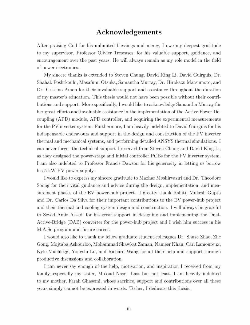
Acknowledgements
After praising God for his unlimited blessings and mercy, I owe my deepest gratitude
to my supervisor, Professor Olivier Trescases, for his valuable support, guidance, and
encouragement over the past years. He will always remain as my role model in the field
of power electronics.
My sincere thanks is extended to Steven Chung, David King Li, David Guirguis, Dr.
Shahab Poshtkouhi, Masafumi Otsuka, Samantha Murray, Dr. Hirokazu Matsumoto, and
Dr. Cristina Amon for their invaluable support and assistance throughout the duration
of my master’s education. This thesis would not have been possible without their contri-
butions and support. More specifically, I would like to acknowledge Samantha Murray for
her great efforts and invaluable assistance in the implementation of the Active Power De-
coupling (APD) module, APD controller, and acquiring the experimental measurements
for the PV inverter system. Furthermore, I am heavily indebted to David Guirguis for his
indispensable endeavours and support in the design and construction of the PV inverter
thermal and mechanical systems, and performing detailed ANSYS thermal simulations. I
can never forget the technical support I received from Steven Chung and David King Li,
as they designed the power-stage and initial controller PCBs for the PV inverter system.
I am also indebted to Professor Francis Dawson for his generosity in letting us borrow
his 5 kW HV power supply.
I would like to express my sincere gratitude to Mazhar Moshirvaziri and Dr. Theodore
Soong for their vital guidance and advice during the design, implementation, and mea-
surement phases of the EV power-hub project. I greatly thank Kshitij Mukesh Gupta
and Dr. Carlos Da Silva for their important contributions to the EV power-hub project
and their thermal and cooling system design and construction. I will always be grateful
to Seyed Amir Assadi for his great support in designing and implementing the Dual-
Active-Bridge (DAB) converter for the power-hub project and I wish him success in his
M.A.Sc program and future career.
I would also like to thank my fellow graduate student colleagues Dr. Shuze Zhao, Zhe
Gong, Mojtaba Ashourloo, Mohammad Shawkat Zaman, Nameer Khan, Carl Lamoureux,
Kyle Muehlegg, Yongshi Lu, and Richard Wang for all their help and support through
productive discussions and collaboration.
I can never say enough of the help, motivation, and inspiration I received from my
family, especially my sister, Mo’oud Nasr. Last but not least, I am heavily indebted
to my mother, Farah Ghasemi, whose sacrifice, support and contributions over all these
years simply cannot be expressed in words. To her, I dedicate this thesis.
iii

Contents
Acknowledgements iii
Table of Contents iv
List of Tables vii
List of Figures viii
1 Introduction 1
1.1 Limiting Factors and Enabling Technologies . . . . . . . . . . . . . . . . 3
1.1.1 Semiconductor Technologies . . . . . . . . . . . . . . . . . . . . . 3
1.1.2 Inverter Topologies . . . . . . . . . . . . . . . . . . . . . . . . . . 6
1.1.3 Control Schemes . . . . . . . . . . . . . . . . . . . . . . . . . . . 8
1.1.4 Power Decoupling . . . . . . . . . . . . . . . . . . . . . . . . . . . 11
1.1.5 Electro-Magnetic Compatibility (EMC) . . . . . . . . . . . . . . . 14
1.2 Emerging Power Modes in EV Inverters: The Power Hub Concept . . . . 16
1.3 Thesis Objectives and Organization . . . . . . . . . . . . . . . . . . . . . 18
1.3.1 System Requirements . . . . . . . . . . . . . . . . . . . . . . . . . 18
1.3.2 Four-Quadrant, Bi-directional, EV Power-Hub . . . . . . . . . . . 19
1.3.3 Modular, High Power Density, Off-Grid PV Inverter . . . . . . . . 20
2 Inverter Architecture and Control 31
2.1 Inverter Electrical Design and Control . . . . . . . . . . . . . . . . . . . 31
2.1.1 BCM, CCM, and Hybrid Operating Modes . . . . . . . . . . . . . 32
2.1.2 Digital Current Modulation . . . . . . . . . . . . . . . . . . . . . 36
2.1.3 Control Logic . . . . . . . . . . . . . . . . . . . . . . . . . . . . . 37
2.1.4 Grid Synchronization . . . . . . . . . . . . . . . . . . . . . . . . . 38
2.2 APD Design and Control . . . . . . . . . . . . . . . . . . . . . . . . . . . 38
2.2.1 Prior Art . . . . . . . . . . . . . . . . . . . . . . . . . . . . . . . 38
iv
2.2.2 Full-Bridge Differential Active Power Decoupling . . . . . . . . . 40
2.2.3 APD Control . . . . . . . . . . . . . . . . . . . . . . . . . . . . . 41
2.2.4 APD Capacitor Size and Volume Optimization . . . . . . . . . . . 43
2.3 Chapter Summary . . . . . . . . . . . . . . . . . . . . . . . . . . . . . . 44
3 EV Power-Hub 48
3.1 Implementation . . . . . . . . . . . . . . . . . . . . . . . . . . . . . . . . 48
3.1.1 Power-Stage . . . . . . . . . . . . . . . . . . . . . . . . . . . . . . 48
3.1.2 DC Bus Capacitor Bank Design . . . . . . . . . . . . . . . . . . . 50
3.1.3 Inductors . . . . . . . . . . . . . . . . . . . . . . . . . . . . . . . 51
3.1.4 EMI Filter . . . . . . . . . . . . . . . . . . . . . . . . . . . . . . . 53
3.1.5 Controller and Isolation . . . . . . . . . . . . . . . . . . . . . . . 56
3.1.6 Auxiliary Power Supply . . . . . . . . . . . . . . . . . . . . . . . 57
3.1.7 Thermal Design . . . . . . . . . . . . . . . . . . . . . . . . . . . . 58
3.2 Experimental Results . . . . . . . . . . . . . . . . . . . . . . . . . . . . . 59
3.2.1 HCMC Operation . . . . . . . . . . . . . . . . . . . . . . . . . . . 59
3.2.2 Parallel SiC MOSFET Operation . . . . . . . . . . . . . . . . . . 60
3.2.3 V2H Operation . . . . . . . . . . . . . . . . . . . . . . . . . . . . 62
3.2.4 V2G/G2V Operation . . . . . . . . . . . . . . . . . . . . . . . . . 62
3.2.5 V2V Operation . . . . . . . . . . . . . . . . . . . . . . . . . . . . 63
3.2.6 Efficiency and Loss Analysis . . . . . . . . . . . . . . . . . . . . . 65
3.3 Chapter Summary . . . . . . . . . . . . . . . . . . . . . . . . . . . . . . 70
4 Modular, Off-grid PV Inverter 74
4.1 Modular, Off-Grid PV Inverter Implementation . . . . . . . . . . . . . . 74
4.1.1 Sub-Inverter Power-Stage and Controller . . . . . . . . . . . . . . 75
4.1.2 Inductors . . . . . . . . . . . . . . . . . . . . . . . . . . . . . . . 76
4.1.3 EMI Filter . . . . . . . . . . . . . . . . . . . . . . . . . . . . . . . 77
4.1.4 APD Capacitor Bank . . . . . . . . . . . . . . . . . . . . . . . . . 79
4.1.5 Auxiliary Power Supply and Interface Board . . . . . . . . . . . . 80
4.1.6 Thermal and Mechanical Design . . . . . . . . . . . . . . . . . . . 81
4.2 Experimental Results . . . . . . . . . . . . . . . . . . . . . . . . . . . . . 84
4.2.1 Single Sub-Inverter Operation . . . . . . . . . . . . . . . . . . . . 84
4.2.2 Multi Sub-Inverter Operation . . . . . . . . . . . . . . . . . . . . 87
4.2.3 Sub-inverter-Shedding . . . . . . . . . . . . . . . . . . . . . . . . 93
4.2.4 Active Power Decoupling . . . . . . . . . . . . . . . . . . . . . . . 94
4.2.5 Transient Response . . . . . . . . . . . . . . . . . . . . . . . . . . 95
v

4.2.6 Loss and Volume Analysis . . . . . . . . . . . . . . . . . . . . . . 96
4.2.7 Benchmark Comparison . . . . . . . . . . . . . . . . . . . . . . . 98
4.3 Chapter Summary . . . . . . . . . . . . . . . . . . . . . . . . . . . . . . 100
5 Conclusions 103
5.1 Thesis Outcomes and Contributions . . . . . . . . . . . . . . . . . . . . . 103
5.2 Future Work . . . . . . . . . . . . . . . . . . . . . . . . . . . . . . . . . . 104
vi
List of Tables
1.1 Comparison of Commonly Used Inverter Topologies . . . . . . . . . . . . 8
1.2 Comparison of Different Current Mode Control Schemes . . . . . . . . . 11
1.3 IEC 61000-3-2 Harmonic Limits for Class A Equipment . . . . . . . . . . 15
1.4 System Requirements for the EV Power-Hub and the PV Inverter . . . . 19
2.1 High-Level Comparison Between the BCM and CCM Operating Modes . 36
3.1 Specifications of the Components Used for the EV Power-Hub . . . . . . 50
3.2 Specifications for the Power-Hub Inductors. Two 25 µH Inductors are
Used for the Line Inductance . . . . . . . . . . . . . . . . . . . . . . . . 52
3.3 Specifications for the Power-Hub Controller Components . . . . . . . . . 57
4.1 Benchmark Comparison of this Work to Five Other Commercial PV String
Inverters with Similar Power-Levels . . . . . . . . . . . . . . . . . . . . . 98
4.2 Benchmark Comparison of this Work to Five Other Academic PV String
Inverters with Similar Power-Levels . . . . . . . . . . . . . . . . . . . . . 99
vii

List of Figures
1.1 US annual solar PV net capacity installations from 2011 to 2015 in Mega
Watts [1]. . . . . . . . . . . . . . . . . . . . . . . . . . . . . . . . . . . . 2
1.2 Comparison of the properties of different semiconductor materials [21–23]. 4
1.3 Application uses for WBG semiconductors [29]. . . . . . . . . . . . . . . 5
1.4 Common single-phase inverter topologies: (a) buck inverter with a low
frequency unfolder stage, (b) full-bridge inverter, and (c) diode-clamped
multi-level inverter. . . . . . . . . . . . . . . . . . . . . . . . . . . . . . . 7
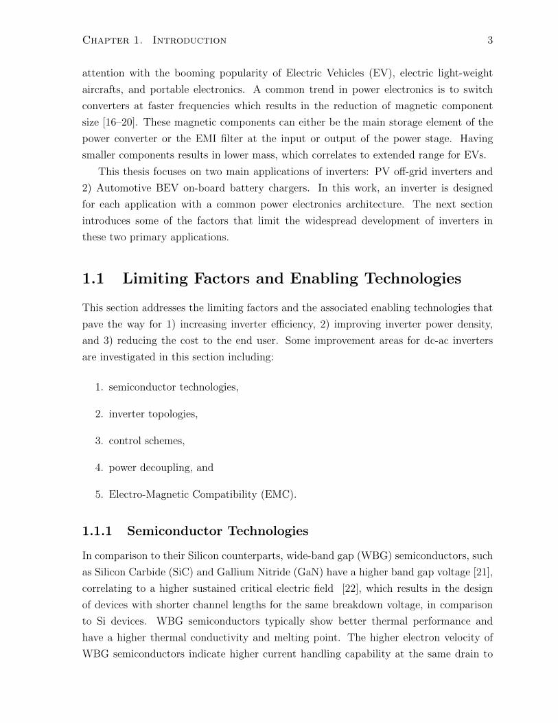
1.5 Different current mode control schemes used in dc-ac converters: (a) CCM,
(b) BCM, (c) DCM, and (d) Hybrid operating modes. . . . . . . . . . . . 10
1.6 Basic waveforms of a typical passive power decoupling stage in a single-
phase inverter application. . . . . . . . . . . . . . . . . . . . . . . . . . . 11
1.7 The effect of bus capacitance on energy storage (volume) and peak-to-peak
voltage ripple. . . . . . . . . . . . . . . . . . . . . . . . . . . . . . . . . . 13
1.8 Quasi-peak emission limits for the CISPR Class A and the CISPR class B
(FCC part 15b) standards. . . . . . . . . . . . . . . . . . . . . . . . . . . 15
1.9 LISN configuration as defined in the CISPR16 standard [63] and the con-
nections with the EUT. . . . . . . . . . . . . . . . . . . . . . . . . . . . . 16
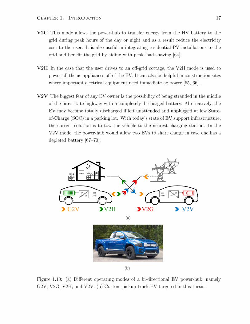
1.10 (a) Different operating modes of a bi-directional EV power-hub, namely
G2V, V2G, V2H, and V2V. (b) Custom pickup truck EV targeted in this
thesis. . . . . . . . . . . . . . . . . . . . . . . . . . . . . . . . . . . . . . 17
1.11 System architecture of the EV power-hub. This thesis only focuses on the
design and implementation of the dc-ac inverter stage. . . . . . . . . . . 20
1.12 System architecture of the PV inverter with three independent sub-inverter/controller
pairs and a dedicated APD module. . . . . . . . . . . . . . . . . . . . . . 21
2.1 Architecture of the full-bridge inverter topology and hysteretic current-
mode controller. . . . . . . . . . . . . . . . . . . . . . . . . . . . . . . . . 32
viii

2.2 Detailed waveforms of the HCMC controller operation in (a) BCM and
(b) CCM. . . . . . . . . . . . . . . . . . . . . . . . . . . . . . . . . . . . 34
2.3 Ipk and Ivly modulation scheme, inductor current, switching frequency
profile, and V1,2 waveforms for the (a) BCM and (b) hybrid operating
modes. . . . . . . . . . . . . . . . . . . . . . . . . . . . . . . . . . . . . . 35
2.4 Block diagram of the digital current modulator . . . . . . . . . . . . . . 37
2.5 Block diagram of the control logic . . . . . . . . . . . . . . . . . . . . . . 38
2.6 Power decoupling topologies: (a) resonant tank, (b) buck, (c) boost, and
(d) stacked capacitor. . . . . . . . . . . . . . . . . . . . . . . . . . . . . . 39
2.7 Proposed full-bridge APD topology with low-side current sense resistor. . 41
2.8 Block diagram of the APD controller. . . . . . . . . . . . . . . . . . . . . 42
2.9 Simulation results of the APD performance with the inverter stage oper-
ating at 2 kW and a 10 Ω series dc input source resistor. The APD phase
is operating at 720 W. . . . . . . . . . . . . . . . . . . . . . . . . . . . . 43
2.10 Total system capacitor volume required versus the amount of APD capac-
itance and the maximum attainable average APD capacitor voltage. The
optimal APD capacitance range is 100-150 µF. . . . . . . . . . . . . . . . 44
3.1 Top side view of the EV power-hub PCB containing the inverter and a
DAB dc-dc converter. The DAB converter is outside the scope of this thesis. 49
3.2 Gate driving circuitry for paralleled SiC MOSFETs. Rg1 is the common
resistance and Rg2 is the individual resistance for each MOSFET. . . . . 50
3.3 Image of the custom made 25 µH, 45 A inductors for the EV power-hub. 52
3.4 Measured ac winding resistance of the EV power-hub inductors with re-
spect to frequency. . . . . . . . . . . . . . . . . . . . . . . . . . . . . . . 52
3.5 Simulated frequency spectrum of the LISN output with the inverter oper-
ating without an EMI filter at 6.6 kW. . . . . . . . . . . . . . . . . . . . 53
3.6 Circuit diagram of the implemented power-hub EMI filter with the asso-
ciated component values. . . . . . . . . . . . . . . . . . . . . . . . . . . . 55
3.7 Simulated input to output current transfer function magnitude and phase
of the power-hub EMI filter. . . . . . . . . . . . . . . . . . . . . . . . . . 55
3.8 Simulated frequency spectrum of the LISN output with the inverter oper-
ating with an EMI filter at 6.6 kW. . . . . . . . . . . . . . . . . . . . . . 56
3.9 Auxiliary power supply for the power-hub. . . . . . . . . . . . . . . . . . 57
ix
3.10 Mechanical and thermal design of the power-hub. The magnetic compo-
nents are cooled with air flow, and the MOSFETs are cooled with the
liquid cooled aluminum chill plate. . . . . . . . . . . . . . . . . . . . . . 58
3.11 HCMC operation with the (a) iL and IR waveforms and instances when the
comparator output signals are asserted in BCM operation. (b) Peak and
valley envelopes for the inductor current for a line cycle in hybrid-mode
operation. . . . . . . . . . . . . . . . . . . . . . . . . . . . . . . . . . . . 60
3.12 Gate to source voltage of a pair of paralleled high-side MOSFETs switching
5 A. . . . . . . . . . . . . . . . . . . . . . . . . . . . . . . . . . . . . . . 61
3.13 (a) power sharing among the first high-side pair MOSFETs, (b) power
sharing among each low-side pair MOSFETs at a power-level of 1 kW. . 61
3.14 Experimental operation of the power-hub in the V2H mode operating in
(a)BCM at a power-level of 2.3 kW, and (b) in hybrid mode at a power-
level of 5 kW. All waveforms are taken with 450 VDC input and an output
of 240 Vrms. . . . . . . . . . . . . . . . . . . . . . . . . . . . . . . . . . . 62
3.15 Experimental operation of the power-hub in the V2G mode operating in
(a)BCM at a power-level of 2.5 kW, and (b) in hybrid mode at a power-
level of 3 kW. Both waveforms are taken with 450 VDC input and an
output of 208 Vrms. . . . . . . . . . . . . . . . . . . . . . . . . . . . . . . 62
3.16 Operation of the EV charger in the (a) dc-dc BCM at 3.4 kW, and (b)
dc-dc CCM operating mode at 5.3 kW. Both waveforms are taken with
450 VDC input and an output of 240 VDC. . . . . . . . . . . . . . . . . 63
3.17 Two power-hubs, which are designed and optimized for ac power transfer,
are setup in the V2V mode to transfer dc power. . . . . . . . . . . . . . . 64
3.18 Measured waveforms demonstrating the operation of two power-hubs in
the V2V operating mode. . . . . . . . . . . . . . . . . . . . . . . . . . . . 64
3.19 Simulated loss breakdown of the power-hub in the (a) dc-ac BCM (2.3
kW), (b) dc-ac BCM/CCM hybrid (5 kW), (c) dc-dc BCM (3.4 kW), and
(d) dc-dc CCM operating mode (5.3 kW). Vin=450 VDC, Vout=340 VDC. 66
3.20 (a) Measured efficiency of the power-hub inverter operating in dc-ac mode
at 240 Vrms and dc-dc BCM and CCM modes at 240 VDC and 340 VDC.
(b) Voltage THD for the V2H operation of the power-hub. . . . . . . . . 67
3.21 (a) Simulated operation of the two power-hubs in V2V mode with (a)
constant DC and (b) bipolar Vlink regulation. Commutating Vlink at 1
Hz results in 16oC lower average and 17oC lower peak MOSFET junction
temperature. . . . . . . . . . . . . . . . . . . . . . . . . . . . . . . . . . . 68
x

3.22 Thermal performance of the power-hub operating in dc-dc mode showing
the temperature of the two low-side MOSFET pairs with (a) constant
dc Vlink regulation, and (b) bipolar Vlink regulation. The optimal Vlink
commutation frequency of 5 Hz results in 6C lower average MOSFET
temperature. . . . . . . . . . . . . . . . . . . . . . . . . . . . . . . . . . . 69
3.23 Measured bipolar Vlink regulation with a commutation frequency of 5 Hz. 69
4.1 (a) Implemented 667 W sub-inverter power-stage. (b) FPGA controller
PCB for each sub-inverter and APD phase. (c) Connection method be-
tween power-stage and controller PCBs and thermal management for every
sub-inverter. . . . . . . . . . . . . . . . . . . . . . . . . . . . . . . . . . . 75
4.2 Image of the custom made 100 µH, 6 A inductors for the off-grid PV inverter. 76
4.3 Measured winding AC resistance of the PV inverter inductors versus fre-
quency. . . . . . . . . . . . . . . . . . . . . . . . . . . . . . . . . . . . . . 77
4.4 Circuit diagram of the implemented PV inverter EMI filter with the asso-
ciated component values. . . . . . . . . . . . . . . . . . . . . . . . . . . . 77
4.5 Simulated input to output current transfer function magnitude and phase
of the PV inverter EMI filter. . . . . . . . . . . . . . . . . . . . . . . . . 78
4.6 Simulated peak frequency spectrum of the LISN output (a) in the absence
of an EMI filter, and (b) with the designed EMI filter included. Both
simulations were carried out at 2 kW output power and the FFT bin
width is set to 1 kHz. . . . . . . . . . . . . . . . . . . . . . . . . . . . . . 78
4.7 Image of the implemented 120 µF ceramic capacitor bank for the APD
module. . . . . . . . . . . . . . . . . . . . . . . . . . . . . . . . . . . . . 79
4.8 Measured performance characteristics of the APD capacitor bank showing
(a) ESR and (b) impedance versus operating frequency. . . . . . . . . . . 80
4.9 (a) Interface PCB top side containing the flat-flex ribbon cable connectors
and the output and APD capacitor voltage sensing ADCs, and (b) interface
PCB bottom side housing the auxiliary power supply. . . . . . . . . . . . 81
4.10 Stage-by-stage mechanical integration of the PV inverter inside a 31 in3
copper custom enclosure resulting in a power density of 64.5 W/in3. . . . 82
4.11 (a) 3D modelled image of the PV inverter, and (b) the final implemented
mechanical prototype of the inverter. . . . . . . . . . . . . . . . . . . . . 83
4.12 (a) Vertical and (b) horizontal cross-sectional views of the inverter de-
picting the airflow direction and passages for inductor and power-stage
cooling. . . . . . . . . . . . . . . . . . . . . . . . . . . . . . . . . . . . . 83
xi
4.13 Cadence simulation testbench for a single sub-inverter. . . . . . . . . . . 85
4.14 Simulation results for the off-grid PV inverter operating in (a) BCM at
a power-level of 254.5 W, and (b) hybrid mode at a power-level of 594
W. Both simulations were carried out with a 450 VDC input voltage and
240 Vrms. . . . . . . . . . . . . . . . . . . . . . . . . . . . . . . . . . . . 85
4.15 Sub-inverter operation (a) in BCM at 330 W (47% rated power) and (b)
in hybrid BCM/CCM operation at 632.7 W (95% rated power). . . . . . 86
4.16 Thermal capture of inductors (left) and power-stage (right) (a) processing
170-W, 25% of rated power in BCM operation only and (b) processing
600-W, 90% of rated power in hybrid-mode operation. . . . . . . . . . . . 86
4.17 Efficiency and THD versus load in pure BCM and hybrid BCM/CCM
operation for a single sub-inverter. . . . . . . . . . . . . . . . . . . . . . . 87
4.18 Mixed-mode Cadence simulation testbench for parallel sub-inverter oper-
ation. . . . . . . . . . . . . . . . . . . . . . . . . . . . . . . . . . . . . . . 88
4.19 Mixed-mode Cadence simulation results for three parallel sub-inverters
operating in (a) BCM at a power rating of 990 W, and (b) hybrid mode
at a power-level of 1.89 kW. . . . . . . . . . . . . . . . . . . . . . . . . . 89
4.20 Experimental open-table style setup for characterizing the multi-sub-inverter
operation of the inverter system. . . . . . . . . . . . . . . . . . . . . . . . 90
4.21 Experimental waveforms of the inverter operation with (a) single sub-
inverter BCM operation at 368 W, and (b) hybrid operation at 660 W. (c)
Dual sub-inverter BCM operation at 736 W, and (d) hybrid operation at
1.32 kW. (e) Tri sub-inverter BCM operation at 1.1 kW, and (f) hybrid
operation at 1.93 kW. All waveforms were captured with 450 VDC input
and 240 Vrms output voltage. . . . . . . . . . . . . . . . . . . . . . . . . 91
4.22 Efficiency and THD versus load in pure BCM and hybrid BCM/CCM
operation with single, two, and three sub-inverters. . . . . . . . . . . . . 92
4.23 Load power vs. reference current trajectory with a positive step in output
power. . . . . . . . . . . . . . . . . . . . . . . . . . . . . . . . . . . . . . 93
4.24 (a) Sub-inverter adding during a positive step in load power, and (b) sub-
inverter shedding during a negative step in load power. . . . . . . . . . . 94
4.25 APD start-up transient with a single sub-inverter operating at 466.7 W.
The APD capacitor voltage reaches a dc offset and ripple voltage of 320
VDC and 54.3 Vpk−pk respectively. This results in a bus voltage ripple
reduction of 42%. . . . . . . . . . . . . . . . . . . . . . . . . . . . . . . . 94
xii

4.26 Volume comparisons of the inverter system with passive power decoupling,
active power decoupling using electrolytic capacitors, and active power
decoupling with ceramic capacitors. . . . . . . . . . . . . . . . . . . . . . 95
4.27 Reference current step response of the inverter from 175 W to 540 W. . . 96
4.28 Simulated loss break down of the PV inverter system in (a) BCM and (b)
hybrid mode operation. (c) Volume breakdown of the PV inverter system. 97
4.29 Comparison of this work to other commercial and academic inverters at the
same power-level. This work achieved a high power density of 64.5 W/in3
with competitive efficiency, manufacturing costs, and reliability in com-
parison to commercial designs. . . . . . . . . . . . . . . . . . . . . . . . . 99
xiii
Chapter 1
Introduction
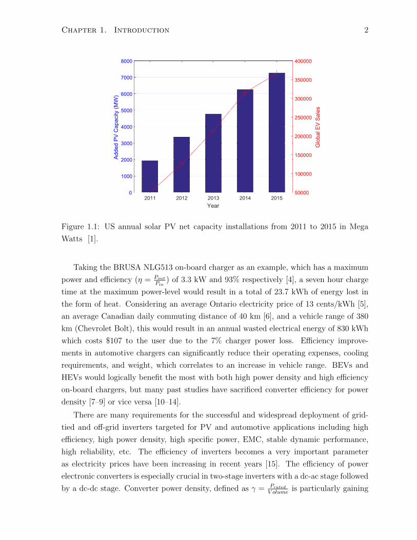
Solar Photo-Voltaic (PV) technology is one of the world’s fastest growing renewable en-
ergy sectors with more than 3.5× increase in US PV capacity from 2011 to 2015, as
shown in Fig. 1.1 [1]. In order to effectively promote the utilization of solar energy, effi-
cient grid-connected power electronics are mandatory. In recent years, the energy sector
has been experiencing a steep trend towards solar electrificaiton of off-grid homes [2],
which requires off-grid inverters to power ac loads. High voltage, string solar inverters
are usually large, heavy and bulky, resulting in increased manufacturing and transporta-
tion costs. Having a compact and light-weight inverter reduces both manufacturing and
initial delivery costs, and also provides the opportunity of being used in automotive and
aerospace applications, where volume and weight cannot be compromised. In addition,
compact inverters with lower volumes and smaller footprints allow easier parallelization
in the case of higher load power demands. In today’s market, 2 kW non-isolated PV
inverters typically have a volume of greater than 280 in3 and sell for more than $1,800
USD.
The field of Hybrid Electric Vehicles (HEV) and Battery Electric Vehicles (BEV), is
a technological area that is heavily reliant on the utility grid. These types of vehicles
depend on the electricity grid to charge their high capacity on-board batteries. Typically,
electric vehicle owners use the late evening hours to charge their car’s battery at power-
levels ranging from 3.3 kW up to 10 kW [3]. HEVs and BEVs usually have a dedicated
on-board charger that are typically used for slow, over-night charging periods.
1
Chapter 1. Introduction 2
50000
100000
150000
200000
250000
300000
350000
400000
Glo
bal E
V Sa
les
2011 2012 2013 2014 2015Year
0
1000
2000
3000
4000
5000
6000
7000
8000
Adde
dPV
Capa
city
(MW
)
Figure 1.1: US annual solar PV net capacity installations from 2011 to 2015 in Mega
Watts [1].
Taking the BRUSA NLG513 on-board charger as an example, which has a maximum
power and efficiency (η = Pout
Pin) of 3.3 kW and 93% respectively [4], a seven hour charge
time at the maximum power-level would result in a total of 23.7 kWh of energy lost in
the form of heat. Considering an average Ontario electricity price of 13 cents/kWh [5],
an average Canadian daily commuting distance of 40 km [6], and a vehicle range of 380
km (Chevrolet Bolt), this would result in an annual wasted electrical energy of 830 kWh
which costs $107 to the user due to the 7% charger power loss. Efficiency improve-
ments in automotive chargers can significantly reduce their operating expenses, cooling
requirements, and weight, which correlates to an increase in vehicle range. BEVs and
HEVs would logically benefit the most with both high power density and high efficiency
on-board chargers, but many past studies have sacrificed converter efficiency for power
density [7–9] or vice versa [10–14].
There are many requirements for the successful and widespread deployment of grid-
tied and off-grid inverters targeted for PV and automotive applications including high
efficiency, high power density, high specific power, EMC, stable dynamic performance,
high reliability, etc. The efficiency of inverters becomes a very important parameter
as electricity prices have been increasing in recent years [15]. The efficiency of power
electronic converters is especially crucial in two-stage inverters with a dc-ac stage followed
by a dc-dc stage. Converter power density, defined as γ = Prated
V olumeis particularly gaining
Chapter 1. Introduction 3
attention with the booming popularity of Electric Vehicles (EV), electric light-weight
aircrafts, and portable electronics. A common trend in power electronics is to switch
converters at faster frequencies which results in the reduction of magnetic component
size [16–20]. These magnetic components can either be the main storage element of the
power converter or the EMI filter at the input or output of the power stage. Having
smaller components results in lower mass, which correlates to extended range for EVs.
This thesis focuses on two main applications of inverters: PV off-grid inverters and
2) Automotive BEV on-board battery chargers. In this work, an inverter is designed
for each application with a common power electronics architecture. The next section
introduces some of the factors that limit the widespread development of inverters in
these two primary applications.
1.1 Limiting Factors and Enabling Technologies
This section addresses the limiting factors and the associated enabling technologies that
pave the way for 1) increasing inverter efficiency, 2) improving inverter power density,
and 3) reducing the cost to the end user. Some improvement areas for dc-ac inverters
are investigated in this section including:
1. semiconductor technologies,
2. inverter topologies,
3. control schemes,
4. power decoupling, and
5. Electro-Magnetic Compatibility (EMC).
1.1.1 Semiconductor Technologies
In comparison to their Silicon counterparts, wide-band gap (WBG) semiconductors, such
as Silicon Carbide (SiC) and Gallium Nitride (GaN) have a higher band gap voltage [21],
correlating to a higher sustained critical electric field [22], which results in the design
of devices with shorter channel lengths for the same breakdown voltage, in comparison
to Si devices. WBG semiconductors typically show better thermal performance and
have a higher thermal conductivity and melting point. The higher electron velocity of
WBG semiconductors indicate higher current handling capability at the same drain to

Chapter 1. Introduction 4
source voltage. Semiconductor materials used in power transistors can be compared and
characterized as presented in Fig. 1.2.
0
0.5
1
1.5
2
2.5
3
Si
SiC
GaN
Electron velocity(x107 cm/s)
Melting point(x 1000 )
Thermal conductivity(x100 W/cm.K)
Electric field strength(MV/cm)
Band gap (eV)
Figure 1.2: Comparison of the properties of different semiconductor materials [21–23].
A brief overview of SiC and GaN semiconductor technologies is presented below:
Silicon Carbide (SiC) technology is very practical when high temperature operation
is mandatory. Having a bandgap voltage of 3.26 eV, a lower variation of intrinsic
carrier density over temperature is achieved [23]. The thermal conductivity of SiC
is 2.3× higher than Si which allows it to have a lower thermal resistance and better
thermal performance, as shown in Fig. 1.2. SiC devices are experimentally verified
to function reliably up to temperatures of 600C [24] and, as opposed to Silicon
devices, the limiting factor for the junction temperature is the device packaging
thermal limit, which is typically bound to 150C [25].
Gallium Nitride (GaN) is another important WBG semiconductor with superior prop-
erties in comparison to Si, namely, high electric field strength, high band gap volt-
age, and higher electron mobility. The only area where GaN is inferior to SiC is
the thermal conductivity. But as GaN MOSFETs are lateral devices as opposed
to SiC, and due to having a thinner substrate, the thermal resistance is brought
very close to, and even better than SiC MOSFETs. Due to the possibility of effec-
tively implanting GaN on Si substrates, GaN ICs can be fabricated using the same
process as Si, resulting in a more economical fabrication process as compared to
SiC. This advantage is a result of the fact that GaN can effectively be implanted

Chapter 1. Introduction 5
on a Si substrate, more commonly known as GaN-On-Silicon technology, bypassing
the need to fabricate extremely expensive GaN substrates. The downside of GaN
devices is the more strict and difficult gate drive requirements which call for a more
accurate and challenging PCB layout. GaN reliability is also a main concern in
high power converters, which brings numerous implementation challenges due to
it’s high gate voltage sensitivity [26–28].
101 102 103 104 105 106
Switching Frequency (Hz)
101
102
103
104
105
106
107
108
Powe
r Rat
ing
(W)
Thyristor
DiscreteIGBT
(SCR)
GTOIEGT
IGBTModule
DiscreteSi-MOSFET
Figure 1.3: Application uses for WBG semiconductors [29].
The application range for Silicon power MOSFETs is typically limited to a switching
frequency of 100 kHz, and a converter power rating of less than 10’s of kW, as shown in
Fig.1.3. It is also followed by the older, more robust IGBT technology, which is limited in
switching frequency and cannot be used in power dense applications. WBG devices are
paving the way for near MHz operation in sub 600 V applications for the first time, which
was unthinkable 10-15 years ago. The fact that converters are now able to switch faster,
corresponds to the reduction in magnetic components volume and space requirements,
which leads to higher power density. The work done in this thesis attempts to leverage
on the superior features of WBG devices to operate at higher switching frequencies and
reduce the size of passive components. This work targets a power-level ranging from 2-10
kW, a 450 V bus voltage, and a variable switching frequency range of 30-300 kHz, as
represented by the green circle in Fig. 1.3.

Chapter 1. Introduction 6
1.1.2 Inverter Topologies
Topology selection greatly affects the density and efficiency of the designed inverter.
To improve the power density of existing 2-10 kW inverters, significant improvements in
inverter topologies and their control are necessary. In this section, a comparative analysis
is presented on three commonly used inverter topologies:
1. dual-stage buck topology with unfolder circuit,
2. full-bridge topology, and
3. diode-clamped multi-level inverter topology.
The dual-stage buck inverter, as illustrated in Fig. 1.4(a), has been extensively studied
in the literature and is commonly implemented in low to medium power dc-ac convert-
ers [30–34]. This topology comprises of a buck converter, which generates a rectified
sinusoidal average current through L, iL(t), followed by a low frequency unfolder stage
which flips the polarity of iL(t) during the negative portions of the ac line cycle. Since
the unfolder MOSFETs switch at the grid frequency, switching losses for M2-M5 are neg-
ligible. If the peak of iL(t) is kept low enough, high efficiency inversion can be achieved
with this topology. The main disadvantage of the buck inverter is the poor grid current
Total Harmonic Distortion (THD) caused due to the unfolder transition points at the
line voltage zero crossings. Another variant of the Buck inverter includes the buck-boost
inverter, as studied extensively in [35, 36], which reduces the THD of the conventional
buck inverter.
The full-bridge inverter topology is a compact and widely used converter capable of
bidirectional power flow, as depicted in Fig. 1.4(b). Since the voltage across L1 and
L2 is bipolar, an unfolder is not needed and an EMI filter is used to inject a low THD
sinusoidal current in to the grid [37–39]. Using conventional sinusoidal Pulse Width
Modulation (PWM) schemes, the full-bridge MOSFETs experience high switching losses
at high power-levels resulting in low efficiency [38]. Using conventional PWM control,
high peak currents through L1 and L2 can be a concern for volume limited applications,
as the inductor must be designed with higher saturation current. Another challenge in
implementing this topology is the way to measure the inductor current, iL(t) in a cost
effective manner. Due to the high common-mode voltages across L1 and L2, shunt current
measurements tend to be very costly. Similarly, hall-effect isolated current measurements
suffer from noise susceptibility and low bandwidth. The dual-buck inverter, also known
as bridgeless inverters, is a derivation of the full-bridge topology which reduces the earth
leakage current and increases the reliability of the inverter [40–42].

Chapter 1. Introduction 7
+
-
M1
L1
D1 C1
+
-
V1
M2
M3 M5
M4
Vgrid
Buck converter Unfolder
iL(t)
iL(t)
t
ig(t)
t
Vdc
(a)
+
-
Cin
M1
M2 M4
M3
Vgrid
Full-bridge converter
ig(t)
t
EMIfilter
iL(t)
t
iL(t)
L1
L2
HF inductors
Vdc
(b)
+
-C2
M1
M4
M3
M2
Vgrid
ig(t)
t
EMI
filter
C1
M5
M8
M7
M6 t
Vo(t)
+-Vo(t)
Vdc
(c)
Figure 1.4: Common single-phase inverter topologies: (a) buck inverter with a low fre-
quency unfolder stage, (b) full-bridge inverter, and (c) diode-clamped multi-level inverter.

Chapter 1. Introduction 8
Multi-level inverter topologies have gained tremendous attention in recent years due
to their numerous advantages [43]. The diode-clamped 5-level inverter, also known as
the Neutral Point Clamp (NPC) inverter, as shown in Fig. 1.4(c), incorporates two series
capacitors to supply the converter with a voltage equivalent to Vdc/2, as well as four
switching devices per leg, each rated at half Vdc. With appropriate switch commuta-
tion, Vo(t) can commutate between five different voltage levels, namely Vdc, −Vdc, Vdc/2,
−Vdc/2, and zero. Having five voltage levels, the output current contains fewer HF har-
monics and has a lower THD, resulting in a lower EMI filter. Each switch has a lower
voltage rating than the full-bridge topology, resulting in smaller switching and conduc-
tion losses. All these benefits come at the cost of higher component count and passive
capacitor balancing requirements [44]. Other variants of this topology include the Flying
Capacitor Circuit (FCC), the isolated Half-Bridge Circuit (HBC) [45], and the Modular
Multi-level Converter (MMC) [46], which include novelties to reduce the disadvantages
of the NPC topology.
The buck inverter topology is not selected in this thesis, since it is not a bi-directional
converter, and suffers from high THD. The physical size of C1 and C2 in the multi-level
converter become very large for medium voltage (100-600 VDC), high power applications
due to the large voltage ripple, as a result multi-level topologies are mainly utilized in
utility scale voltage (≥ 100 kV) dc-ac conversion applications. The full-bridge inverter
topology is an attractive converter for this thesis due to the low part count and higher
achievable density. As will be explained in chapter 2, a single low side shunt resistor is
utilized to reduce sensing cost.
A comparison between the topologies for a dc input voltage of 400 VDC, and a power
level of 2 kW ≤ P ≤ 10 kW is presented in table 1.1.
Table 1.1: Comparison of Commonly Used Inverter Topologies
Topology Density Efficiency THD
Two-stage buck Medium Medium High
Full-bridge High High Medium
Multi-level Low High Low
1.1.3 Control Schemes
Conventional sinusoidal PWM control, as discussed in [47], faces many design challenges
in high power density dc-ac converters, particularly due to MOSFET hard switching.

Chapter 1. Introduction 9
This directly relates to larger heat sinks, lower efficiency, and a lower power density. As
a result, current mode controlled inverters have become more popular as designers are
able to achieve soft-switching, depending on the type of controller implementation. Some
other benefits of current-mode control include:
• inherent over current protection,
• accurate current sharing in parallel converter operation,
• high line-to-output rejection ratio, and
• simpler voltage-loop control due to first order plant dynamics.
Current mode control schemes come with the drawback of more complex controller
implementations and susceptibility to external and switching noise. However, the nu-
merous advantages offered, significantly outweigh the extra complexities and with proper
shielding, noise immunity can be achieved. There are three main operating modes for
current mode controllers: 1) Continuous Conduction Mode (CCM), 2) Boundary Conduc-
tion Mode (BCM), and 3) Discontinuous Conduction Mode (DCM), as shown in Fig. 2.2.
In this section, a brief comparative discussion is presented involving the limitations of
each operating mode, and the introduction of a hybrid mode to reduce the limitation of
each current control scheme.
The CCM operating mode is when the peak and the valley of the inductor current are
both positive or both negative resulting in the smallest ripple current and lower magnetic
losses in comparison with the BCM and DCM operating modes. Switching losses, how-
ever, are significantly greater due to the lack of soft-switching at the current valley points
hence, WBG semiconductors are very beneficial in CCM controlled converters. The DCM
operating mode is typically utilized in flyback or push-pull based inverters [48], and oc-
curs when iL remains zero for a small fraction of the switching period. For the same
average current as CCM, DCM results in higher inductor RMS currents and core losses,
leading to bulky, over-designed magnetic components. BCM occurs at the boundary of
DCM and CCM operating modes and as with DCM, results in fairly high inductor RMS
currents [37, 49, 50]. However, similar to DCM, soft-switching is easily attainable, which
leads to lower switching losses.
Chapter 1. Introduction 10
t
iL(t)
(a)
t
iL(t)
(b)
t
iL(t)
(c)
t
iL(t)
(d)
Figure 1.5: Different current mode control schemes used in dc-ac converters: (a) CCM,
(b) BCM, (c) DCM, and (d) Hybrid operating modes.
To utilize the soft-switching benefits of BCM and the low inductor current ripple
advantages of CCM, a hybrid operating mode for dc-ac inverters is presented in this
thesis, involving the combination of BCM and CCM during a single ac line cycle, as
shown in Fig. 1.5(d). In this mode, soft-switching is maintained near the line voltage zero-
crossings by operating in BCM, and the current controller switches to CCM at the peaks
and troughs of the line voltage to prevent very high peak currents through the inductors.
This allows the utilization of inductors with a lower saturation current, hence, leading to
smaller sized magnetics. Past studies on multi-mode current modulation involve similar
techniques to reduce converter loss and volume. In [51], a three-mode DCM/BCM/CCM
current mode controller is implemented on a 150 W, 1 MHz, PFC boost rectifier with
GaN technology. A BCM dual-mode ZVS/ZCS current control scheme is introduced
in [52], in which the controller sets the valley current limit below zero near the zero
crossings and at zero near the peaks and troughs of the ac line-cycle. A comparative
summary of the four operating modes is presented in table 1.2
Chapter 1. Introduction 11
Table 1.2: Comparison of Different Current Mode Control Schemes
CCM BCM/DCM Hybrid
Core losses Low High Medium
Switching losses High Low Medium
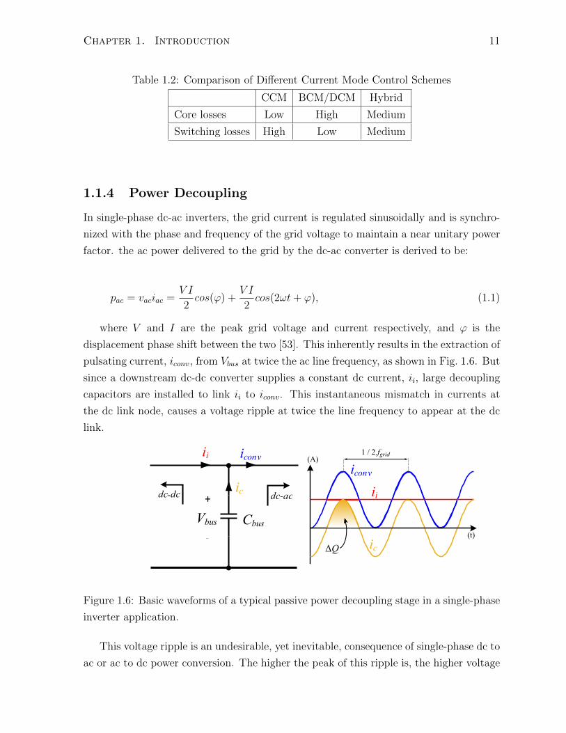
1.1.4 Power Decoupling
In single-phase dc-ac inverters, the grid current is regulated sinusoidally and is synchro-
nized with the phase and frequency of the grid voltage to maintain a near unitary power
factor. the ac power delivered to the grid by the dc-ac converter is derived to be:
pac = vaciac =V I
2cos(ϕ) +
V I
2cos(2ωt+ ϕ), (1.1)
where V and I are the peak grid voltage and current respectively, and ϕ is the
displacement phase shift between the two [53]. This inherently results in the extraction of
pulsating current, iconv, from Vbus at twice the ac line frequency, as shown in Fig. 1.6. But
since a downstream dc-dc converter supplies a constant dc current, ii, large decoupling
capacitors are installed to link ii to iconv. This instantaneous mismatch in currents at
the dc link node, causes a voltage ripple at twice the line frequency to appear at the dc
link.
CbusVbus
+
-
ic
ii iconv
dc-ac
ic
iconv
ii
ΔQ
dc-dc
1 / 2.fgrid(A)
(t)
Figure 1.6: Basic waveforms of a typical passive power decoupling stage in a single-phase
inverter application.
This voltage ripple is an undesirable, yet inevitable, consequence of single-phase dc to
ac or ac to dc power conversion. The higher the peak of this ripple is, the higher voltage

Chapter 1. Introduction 12
rating is needed for the power switches, which directly correlates to cost and converter
efficiency. In PV applications, a voltage ripple on the output of the solar cells mean that
there is a larger deviation from the Maximum Power Point (MPP), which leads to a lower
MPPT efficiency. In order to alleviate this side-effect, electrolytic capacitor banks are
commonly utilized, which are bulky and reduce the life-time of the converter. The lifetime
and durability of different capacitors vary greatly depending on the type of technology
utilized. For example, electrolytic capacitors usually have a shorter lifetime than ceramic
capacitors, typically 1000 hours at 105C operating temperature [54]. The downside
of ceramic capacitors is their higher cost. For example, at a voltage rating of 500 V,
a 1 µF ceramic capacitor is greater than 9 times more expensive than the equivalent
electrolytic type. Having power density in mind, the volume of this capacitor bank must
be optimized. The volume of a capacitor is directly proportional to the maximum energy
that can be stored, which is given by:
E =1
2CV 2, (1.2)
and the voltage ripple on a capacitor is directly related to the total charge, ∆Q,
cycling through a capacitor, as shown in Fig. 1.6, by:
∆V =∆Q
C(1.3)
where ∆Q is easily obtained by integrating the capacitor current, ic, over half the
second harmonic period:
∆Q =
∫ T120Hz2
0
icdt =
∫ T120Hz2
0
sin(120Hz × t)dt (1.4)
which results in 13.3 mC of charge for an inverter operating at 2 kW. Combining (1.2)
and (1.3) to find the overall energy storage requirements for the dc link capacitor yields:
E =1
2C(V + ∆V )2 =
1
2C(V +
∆Q
C)2 (1.5)
After substituting the result of (1.4) into (1.5), the plot of (1.5) and (1.3) is shown
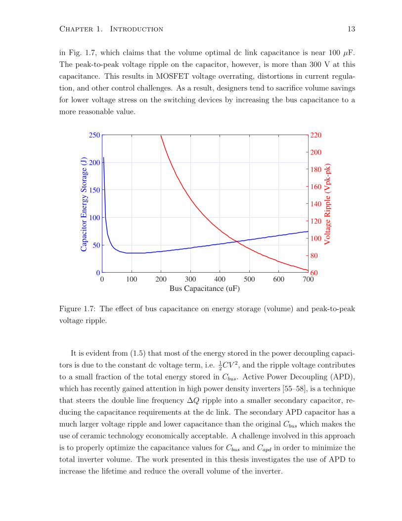
Chapter 1. Introduction 13
in Fig. 1.7, which claims that the volume optimal dc link capacitance is near 100 µF.
The peak-to-peak voltage ripple on the capacitor, however, is more than 300 V at this
capacitance. This results in MOSFET voltage overrating, distortions in current regula-
tion, and other control challenges. As a result, designers tend to sacrifice volume savings
for lower voltage stress on the switching devices by increasing the bus capacitance to a
more reasonable value.
0 100 200 300 400 500 600 700
Bus Capacitance (uF)
0
50
100
150
200
250
Cap
acit
or
En
erg
y S
tora
ge
(J)
60
80
100
120
140
160
180
200
220
Vo
ltag
e R
ipp
le (
Vp
k-p
k)
Figure 1.7: The effect of bus capacitance on energy storage (volume) and peak-to-peak
voltage ripple.
It is evident from (1.5) that most of the energy stored in the power decoupling capaci-
tors is due to the constant dc voltage term, i.e. 12CV 2, and the ripple voltage contributes
to a small fraction of the total energy stored in Cbus. Active Power Decoupling (APD),
which has recently gained attention in high power density inverters [55–58], is a technique
that steers the double line frequency ∆Q ripple into a smaller secondary capacitor, re-
ducing the capacitance requirements at the dc link. The secondary APD capacitor has a
much larger voltage ripple and lower capacitance than the original Cbus which makes the
use of ceramic technology economically acceptable. A challenge involved in this approach
is to properly optimize the capacitance values for Cbus and Capd in order to minimize the
total inverter volume. The work presented in this thesis investigates the use of APD to
increase the lifetime and reduce the overall volume of the inverter.

Chapter 1. Introduction 14
1.1.5 Electro-Magnetic Compatibility (EMC)
With increasing converter switching frequencies and with switches capable of causing
higher dv/dt and di/dt transitions, Electro-Magnetic Compatibility (EMC) becomes an
important design criteria for Switch-Mode Power Supplies (SMPS). There are two main
forms of Electro-Magnetic Interference (EMI):
1. Radiated EMI, and
2. Conducted EMI [59].
Radiated EMI are radio-frequency emissions of a SMPS that propagate through air
and can potentially cause disturbances in other electronic radio devices. Certain stan-
dards, such as FCC, CISPR22, and MIL-STD-461E [60], define the maximum allowable
radiated EMI according to a set of measurement rules. Radiated EMI is usually mea-
sured by placing the Equipment Under Test (EUT) in a semianechoic chamber which
isolates the EUT from unwanted external and reflected emissions. According to FCC, a
quasi-peak detector is placed 3 meters away from the EUT to receive the emitted EMI
up to a frequency of 18 GHz [59].
The main purpose of Conducted EMI restrictions is, to limit the higher order
harmonic currents flowing through the product’s ac power cable. If an inverter emits
high frequency noise currents in to the ac grid, the utility network behaves as an antenna
and eventually results in wide-scale radiated EMI. The IEC 61000-3-2 standard [61]
defines the maximum allowable harmonic magnitude values for the output ac current, as
summarized in table 1.3. The FCC and CISPR22 standards [62] provide limits on the
frequency spectrum of the injected noise current. The current limits for commercial and
residential equipment are defined under CISPR Class A and Class B, respectively, and
are shown in Fig. 1.8
Compliant SMPS designs must have low radiated and conducted EMI emissions
and susceptibility. EMI emissions is a measure of how much a SMPS is polluting the
environment and other electronic devices. This form of EMI compliance is a major focus
in this thesis. EMI susceptibility, which is outside the scope of this thesis, is a measure
of how immune a SMPS is to externally generated radiated and conducted EMI.

Chapter 1. Introduction 15
Table 1.3: IEC 61000-3-2 Harmonic Limits for Class A Equipment
Harmonic order Maximum permissible
n harmonic current (A)
Odd harmonics
3 2.30
5 1.14
7 0.77
9 0.40
11 0.33
13 0.21
15 ≤ n ≤ 39 0.15 15n
Even harmonics
2 1.08
4 0.43
6 0.30
8 ≤ n ≤ 40 0.23 8n
10-1 100 101 10220
30
40
50
60
70
80
90
100
Frequency (MHz)
Cond
ucte
d em
issio
n (d
BV
)
79
0.15
66
56
0.5 5
73
60
30
CISPR Class AQP limit
CISPR Class BQP limit (FCC part 15b)
Figure 1.8: Quasi-peak emission limits for the CISPR Class A and the CISPR class B
(FCC part 15b) standards.
In order to accurately measure conducted EMI, a Line Impedance Stabilization Net-
work (LISN) is placed in series with the EUT ac output port and the grid. There are two
main purposes to a LISN: 1) to prevent external noise from contaminating the measure-
ment, and 2) to provide a constant impedance in frequency between phase and ground

Chapter 1. Introduction 16
and between neutral and ground as seen by the EUT into the power cord from site to site.
A LISN as specified by the CISPR16 standard and the setup configuration is shown in
Fig. 1.9. The LISN contains a passive high-pass filter consisting of C1 and R1 to limit the
frequency range of the measured signal to within the standard specification and to also
provide 50 Ω termination. The output of the LISN is connected to a spectrum analyser
in quasi-peak detection mode and a frequency bin width of 9 kHz.
50H 250H
50H 250H
250nF
50
8F 4F
5 10
50 5 10
250nF 8F 4 F
EUT
CISPR16 LISN
Live
Neutral
Earth
Spectrum analyser
Live
Earth
Neutral
Vsense
Vsense
Figure 1.9: LISN configuration as defined in the CISPR16 standard [63] and the connec-
tions with the EUT.
1.2 Emerging Power Modes in EV Inverters: The
Power Hub Concept
With the recent improvements in power converter topologies and control, bi-directional
EV power-hubs are gaining more attention in recent years. With four-quadrant inverter
operation, active power can be supplied to and received from the ac grid using the high
voltage EV battery. The charger can also provide reactive power support, both at the line
frequency and also for compensating harmonics within the vicinity of the EV. This feature
can transform a conventional on-board EV charger into a power-hub capable of operating
in the Grid-to-Vehicle (G2V), Vehicle-to-Grid (V2G), Vehicle-to-House (V2H), Vehicle-
to-Vehicle (V2V), and VAR compensation operating modes, as shown in Fig. 1.10(a).
G2V This mode is similar to most conventional EV battery chargers available in the
market. In this mode, the power-hub charges the battery with a constant dc current,
and also perform Power Factor Correction (PFC) on the grid voltage and current.
Chapter 1. Introduction 17
V2G This mode allows the power-hub to transfer energy from the HV battery to the
grid during peak hours of the day or night and as a result reduce the electricity
cost to the user. It is also useful in integrating residential PV installations to the
grid and benefit the grid by aiding with peak load shaving [64].
V2H In the case that the user drives to an off-grid cottage, the V2H mode is used to
power all the ac appliances off of the EV. It can also be helpful in construction sites
where important electrical equipment need immediate ac power [65, 66].
V2V The biggest fear of any EV owner is the possibility of being stranded in the middle
of the inter-state highway with a completely discharged battery. Alternatively, the
EV may become totally discharged if left unattended and unplugged at low State-
of-Charge (SOC) in a parking lot. With today’s state of EV support infrastructure,
the current solution is to tow the vehicle to the nearest charging station. In the
V2V mode, the power-hub would allow two EVs to share charge in case one has a
depleted battery [67–70].
DC
AC
DC
AC
G2V V2H V2G V2V
(a)
(b)
Figure 1.10: (a) Different operating modes of a bi-directional EV power-hub, namely
G2V, V2G, V2H, and V2V. (b) Custom pickup truck EV targeted in this thesis.
Chapter 1. Introduction 18
1.3 Thesis Objectives and Organization
The goal of this thesis is to design and implement two inverter prototypes: 1) a four-
quadrant, grid-tied EV power-hub, and 2) a modular, high power density, off-grid PV
inverter. The EV power-hub design is targeted for an on-board HV Li-ion battery pack
in a fully electric pick-up truck, as depicted in Fig. 1.10(b), while introducing the newer
control modes such as V2G, V2H, and V2V, and meeting stringent EMI requirements.
The goal in the PV inverter project is to build a non-isolated, off-grid 2 kW inverter
for the highest possible power density using SiC technology and a modular architecture,
while leveraging the same control techniques from the EV power-hub. The objective of
the modular approach is to spread the generated heat over a larger surface area and
improve light-load efficiency by turning off redundant modules when not needed at lower
power-levels. The modular design also improves the reliability of the inverter by providing
extra redundancy in power-stage units. The main goal of the PV inverter project is to
push the boundaries of power density and conversion efficiency, as a result cost is not the
most important consideration for this project.
1.3.1 System Requirements
The system requirements and specifications for the PV inverter originate from the Google
Little Box (GLB) challenge which was a worldwide competition, run by Google and
IEEE’s power electronics society, to build the most power dense off-grid inverter rated at
2 kW. The GLB challenge began in July 2014 and ended, after nearly 2 years, in March
2016 with 18 finalists from around the world. The EV power-hub needs to meet, EMI,
and other automotive requirements in a cost sensitive way, hence, power density is not
the primary focus. The main system requirements for the EV power-hub and the PV
inverter are shown in table 1.4.
While all the GLB challenge finalists used GaN technology, this work utilized SiC
devices for increased reliability without significantly sacrificing power density. Since the
PV inverter does not contain a dc-dc converter as a second stage to perform MPPT and
regulate the PV string voltage and current, the dc-ac stage must limit the input voltage
ripple, using APD, to maintain a high MPPT efficiency. While topics concerning MPPT
algorithms fall outside the scope of this thesis, minimising input voltage and current
ripple for the PV inverter is a significant focus. The EV power-hub has a noticeably
higher minimum volume requirement due to having a higher power-level and containing
an isolated dc-dc converter which is not considered in this work.

Chapter 1. Introduction 19
Table 1.4: System Requirements for the EV Power-Hub and the PV Inverter
ParameterEV power-hub PV inverter
Unitsection 1.3.2 section 1.3.3
Input voltage, Vin 450 VDC
Output voltage, Vac 240 VRMS
Peak power 6.6 2 kVA
Input voltage ripple 3 %
Input current ripple 20 %
Minimum CEC efficiency 95 %
Maximum average voltage THD,
THDv
5 %
Maximum average current THD,
THDi
5 %
Maximum inverter volume 380 40 in3
Maximum exterior temperature 60 C
Modular No Yes -
Grid-tied? Yes No -
Bi-directional Yes Yes -
Cooling Liquid Air -
1.3.2 Four-Quadrant, Bi-directional, EV Power-Hub
The EV power-hub, implemented with paralleled SiC MOSFETs for increased current
handling capability, is intended for use in a full-electric pick-up truck prototype, as
shown in Fig. 1.10(b), with a fully custom HV Li-ion battery pack. The inverter stage
is preceded by a Dual-Active-Bridge (DAB) dc-dc converter which regulates the battery
current and voltage, as shown in Fig. 1.11. The high level control module is responsible
for interfacing between the power-hub and the rest of the on-board vehicle power systems
and sending the necessary commands to the dc-ac and dc-dc converters such as mode
selection and power measurements. The implemented design is capable of bi-directional
operation which allows it to process ac power in all four quadrants. As shown earlier in
Fig. 1.10(a) the power-hub operates in four distinct modes: G2V, V2G, V2H and the
newer V2V mode.

Chapter 1. Introduction 20
DC
DC
DC
AC
Cbus
Vbat380 - 480
VDC321-449
VDC
Controls battery charging/discharging process
Regulates Vbus
Performs PFC
High Level ControlCAN bus
240 VRMS Grid
Li-ion HV Thesis focus
+
_
battery pack
Vbus
+
_
Figure 1.11: System architecture of the EV power-hub. This thesis only focuses on the
design and implementation of the dc-ac inverter stage.
Each of the high level controller, dc-ac, and dc-dc converter are powered from a set of
completely isolated power planes for user safety and converter protection which enhances
the power-hub reliability. The power-hub inverter performs PFC on the ac side and
variable dc bus voltage regulation depending on the battery terminal voltage to ensure
that the DAB converter is operating at the most efficient voltage conditions.
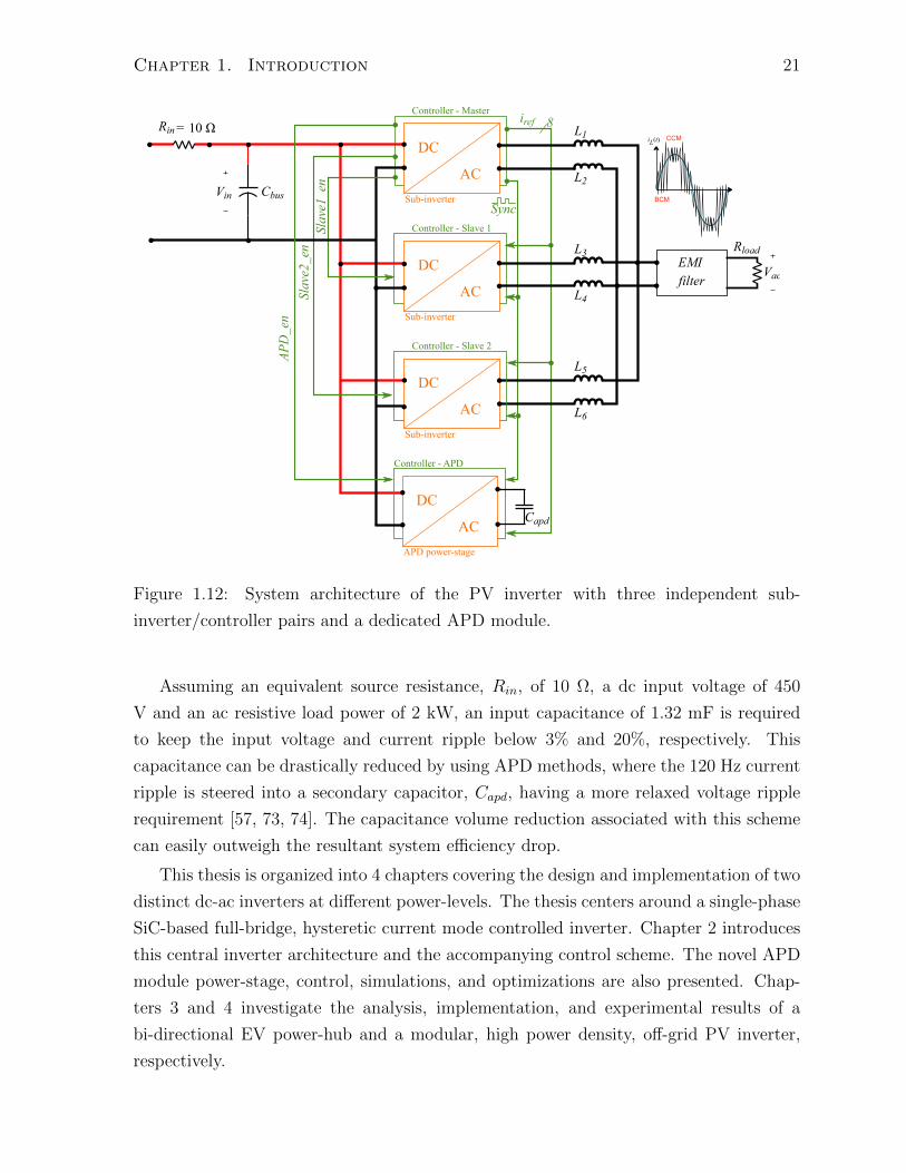
1.3.3 Modular, High Power Density, Off-Grid PV Inverter
The proposed system architecture for the off-grid PV inverter is shown in Fig. 1.12. A
modular approach is used to optimize the mechanical design by distributing the thermal
losses throughout the inverter’s volume. Three independently controlled sub-inverters,
each designed for a rated power of 0.67 kVA, are connected in parallel and share a common
EMI filter to generate a low-THD ac output voltage, Vac. The master controller provides
a 60 Hz synchronization pulse to the slave controllers to allow for phase locking. The
digital current reference is communicated by the master to the slave sub-inverters as part
of the outer voltage-loop. An interface board is used to route multiple control signals
and to distribute various auxiliary voltage supplies needed for the digital controllers,
sensors and data-converters. Redundant sub-inverters can be turned off at light loads
for improved efficiency, which is commonly referred to as phase-shedding in multi-phase
dc-dc converters [71, 72].
Chapter 1. Introduction 21
Sub-inverter
Controller - Master
DC
AC
Sub-inverter
Controller - Slave 1
DC
AC
Cbus
L1
L2
L3
L4
L5
L6
EMIfilter
Sync
iref 8
Sub-inverter
Controller - Slave 2
DC
AC
APD power-stage
Controller - APD
DC
AC Capd
Slav
e1_e
nSl
ave2
_en
APD
_en
Rload
Vin
Vac
Rin = 10 Ω
Figure 1.12: System architecture of the PV inverter with three independent sub-
inverter/controller pairs and a dedicated APD module.
Assuming an equivalent source resistance, Rin, of 10 Ω, a dc input voltage of 450
V and an ac resistive load power of 2 kW, an input capacitance of 1.32 mF is required
to keep the input voltage and current ripple below 3% and 20%, respectively. This
capacitance can be drastically reduced by using APD methods, where the 120 Hz current
ripple is steered into a secondary capacitor, Capd, having a more relaxed voltage ripple
requirement [57, 73, 74]. The capacitance volume reduction associated with this scheme
can easily outweigh the resultant system efficiency drop.
This thesis is organized into 4 chapters covering the design and implementation of two
distinct dc-ac inverters at different power-levels. The thesis centers around a single-phase
SiC-based full-bridge, hysteretic current mode controlled inverter. Chapter 2 introduces
this central inverter architecture and the accompanying control scheme. The novel APD
module power-stage, control, simulations, and optimizations are also presented. Chap-
ters 3 and 4 investigate the analysis, implementation, and experimental results of a
bi-directional EV power-hub and a modular, high power density, off-grid PV inverter,
respectively.

Chapter 1. Introduction 22
The current-mode control scheme and the central architecture is initially implemented
and verified on the EV power-hub with lower density requirements. The PV inverter im-
plements the main inverter architecture in a modular format with a priority on achieving
high power density and light load efficiency. The APD module is only implemented in
the PV inverter project to reduce the size of the dc bus capacitors.

References
[1] “Us net annual pv installation,” National Renewable Energy Laboratory Website,
available http://www.nrel.gov/docs/fy17osti/66591.pdf/.
[2] “Trends in renewable resources for off-grid communities,” Price Water
House Coopers Website, available https://www.pwc.com/gx/en/energy-utilities-
mining/pdf/electricity-beyond-grid.pdf.
[3] “Electric car charging 101 ? types of charging, charging networks, apps, and more,”
EV Obsession Website, available https://evobsession.com/electric-car-charging-101-
types-of-charging-apps-more/.
[4] “Brusa nlg513 on-board ev charger data sheet,” BRUSA Website, available
http://www.brusa.biz/fileadmin/template.
[5] “Ontario residential electricity rates,” Ontario Energy Board Website, available
https://www.oeb.ca/rates-and-your-bill/electricity-rates.
[6] “Average commuting times in canada,” Statistics Canada Website, available
http://www12.statcan.gc.ca/nhs-enm/2011/as-sa/99-012-x/99-012-x2011003 1-
eng.cfm.
[7] R. Hou and A. Emadi, “A primary full-integrated active filter auxiliary power module
in electrified vehicles with single-phase onboard chargers,” IEEE Transactions on
Power Electronics, vol. 32, no. 11, pp. 8393–8405, Nov 2017.
[8] Y. Murakami, Y. Tajima, and S. Tanimoto, “Air-cooled full-sic high power density
inverter unit,” in 2013 World Electric Vehicle Symposium and Exhibition (EVS27),
Nov 2013, pp. 1–4.
[9] E. Mickus, T. T. Vu, and T. O’Donnell, “A low-profile, high power density inverter
with minimal energy storage requirement for ripple cancellation,” in 2016 IEEE 7th
23
REFERENCES 24
International Symposium on Power Electronics for Distributed Generation Systems
(PEDG), June 2016, pp. 1–7.
[10] A. Trubitsyn, B. J. Pierquet, A. K. Hayman, G. E. Gamache, C. R. Sullivan, and
D. J. Perreault, “High-efficiency inverter for photovoltaic applications,” in 2010
IEEE Energy Conversion Congress and Exposition, Sept 2010, pp. 2803–2810.
[11] R.-Y. Duan and C.-T. Chang, “A novel high-efficiency inverter for stand-alone and
grid-connected systems,” in 2008 3rd IEEE Conference on Industrial Electronics and
Applications, June 2008, pp. 557–562.
[12] W. Y. Choi, “High-efficiency single-phase three-level bidirectional inverter,” in 2017
IEEE 18th Workshop on Control and Modeling for Power Electronics (COMPEL),
July 2017, pp. 1–3.
[13] J. S. Kim, J. M. Kwon, and B. H. Kwon, “High-efficiency two-stage three-level
grid-connected photovoltaic inverter,” IEEE Transactions on Industrial Electronics,
vol. PP, no. 99, pp. 1–1, 2017.
[14] W. Yu, J. S. J. Lai, H. Qian, and C. Hutchens, “High-efficiency mosfet inverter with
h6-type configuration for photovoltaic nonisolated ac-module applications,” IEEE
Transactions on Power Electronics, vol. 26, no. 4, pp. 1253–1260, April 2011.
[15] T. Jackson, A. Stedman, E. Aliakbari, and K. P. Green, “Evaluating
electricity price growth in ontario,” Fraser Institute Website, 2017, avail-
able https://www.fraserinstitute.org/sites/default/files/evaluating-electicity-price-
growth-in-ontario.pdf.
[16] B. Whitaker, A. Barkley, Z. Cole, B. Passmore, T. McNutt, and A. B. Lostetter,
“High-frequency ac-dc conversion with a silicon carbide power module to achieve
high-efficiency and greatly improved power density,” in 2013 4th IEEE International
Symposium on Power Electronics for Distributed Generation Systems (PEDG), July
2013, pp. 1–5.
[17] K. Shirabe, M. M. Swamy, J. K. Kang, M. Hisatsune, Y. Wu, D. Kebort, and
J. Honea, “Efficiency comparison between si-igbt-based drive and gan-based drive,”
IEEE Transactions on Industry Applications, vol. 50, no. 1, pp. 566–572, Jan 2014.
[18] X. Huang, Z. Liu, Q. Li, and F. C. Lee, “Evaluation and application of 600 v gan
hemt in cascode structure,” IEEE Transactions on Power Electronics, vol. 29, no. 5,
pp. 2453–2461, May 2014.

REFERENCES 25
[19] M. Acanski, J. Popovic-Gerber, and J. A. Ferreira, “Comparison of si and gan power
devices used in pv module integrated converters,” in 2011 IEEE Energy Conversion
Congress and Exposition, Sept 2011, pp. 1217–1223.
[20] J. Biela, M. Schweizer, S. Waffler, and J. W. Kolar, “Sic versus si - evaluation of
potentials for performance improvement of inverter and dc - dc converter systems
by sic power semiconductors,” IEEE Transactions on Industrial Electronics, vol. 58,
no. 7, pp. 2872–2882, July 2011.
[21] C. Hu, Modern Semiconductor Devices for Integrated Circuits, 2nd edition. Prentice
Hall, 2010.
[22] L. Efthymiou, G. Camuso, G. Longobardi, F. Udrea, E. Lin, T. Chien, and M. Chen,
“Zero reverse recovery in sic and gan schottky diodes: A comparison,” in 2016 28th
International Symposium on Power Semiconductor Devices and ICs (ISPSD), June
2016, pp. 71–74.
[23] F. Qi, L. Fu, L. Xu, P. Jing, G. Zhao, and J. Wang, “Si and sic power mosfet char-
acterization and comparison,” in 2014 IEEE Conference and Expo Transportation
Electrification Asia-Pacific (ITEC Asia-Pacific), Aug 2014, pp. 1–6.
[24] P. Vaculik, “The properties of sic in comparison with si semiconductor devices,” in
2013 International Conference on Applied Electronics, Sept 2013, pp. 1–4.
[25] “Cree 900v sic mosfet,” CREE-Wolfspeed Datasheet, available
http://www.wolfspeed.com/media/downloads/145/C3M0065090J.pdf.
[26] R. Mitova, A. Dentella, D. Reilly, O. Miquel, and X. Blanchard, “Current trends for
gan on si power devices for industrial applications,” in CIPS 2016; 9th International
Conference on Integrated Power Electronics Systems, March 2016, pp. 1–11.
[27] M. Sun, M. Pan, X. Gao, and T. Palacios, “Vertical gan power fet on bulk gan
substrate,” in 2016 74th Annual Device Research Conference (DRC), June 2016,
pp. 1–2.
[28] D. Mishra, V. Arora, L. Nguyen, S. Iriguchi, H. Sada, L. Clemente, S. Lim, H. Lin,
A. Lohia, S. Gurrum, J. Sauser, and S. Spencer, “Packaging innovations for high
voltage (hv) gan technology,” in 2017 IEEE 67th Electronic Components and Tech-
nology Conference (ECTC), May 2017, pp. 1480–1484.

REFERENCES 26
[29] C. Sintamarean, E. Eni, F. Blaabjerg, R. Teodorescu, and H. Wang, “Wide-band
gap devices in pv systems - opportunities and challenges,” in 2014 International
Power Electronics Conference (IPEC-Hiroshima 2014 - ECCE ASIA), May 2014,
pp. 1912–1919.
[30] S. POTHARAJU, “Solar inverter,” U.S. Patent 9 270 201, Feb. 23, 2016.
[31] M. Andrew, D. Rooij, J. S. Glaser, O. G. Mayer, and S. F. S. El-Barbari,
“Quasi-ac, photovoltaic module for unfolder photovoltaic inverter,” U.S. Patent
US20 100 071 742A1, Mar. 25, 2010.
[32] M. Andrew, D. Rooij, J. S. Glaser, and R. L. Steigerwald, “High efficiency photo-
voltaic inverte,” U.S. Patent 9 270 201, Sep. 20, 2011.
[33] M. Joshi, E. Shoubaki, R. Amarin, B. Modick, and J. Enslin, “A high-efficiency
resonant solar micro-inverter,” in Proceedings of the 2011 14th European Conference
on Power Electronics and Applications, Aug 2011, pp. 1–10.
[34] V. Pandya and A. K. Agarwala, “Efficient pv micro-inverter with isolated output,”
in 2012 IEEE Fifth Power India Conference, Dec 2012, pp. 1–5.
[35] T. Zhu, L. Zhang, R. Gao, and L. Qu, “A semi-two-stage dual-buck transformerless
pv grid-tied inverter,” in 2017 IEEE Applied Power Electronics Conference and
Exposition (APEC), March 2017, pp. 391–396.
[36] Z. Zhao, M. Xu, Q. Chen, J. S. Lai, and Y. Cho, “Derivation, analysis, and imple-
mentation of a boost 2013;buck converter-based high-efficiency pv inverter,” IEEE
Transactions on Power Electronics, vol. 27, no. 3, pp. 1304–1313, March 2012.
[37] J. Wang, D. Zhang, J. Li, Z. Lv, and Y. Li, “Digital zvs bcm current controlled single-
phase full-bridge inverter using dsp tms320f28035,” in 2017 IEEE 3rd International
Future Energy Electronics Conference and ECCE Asia (IFEEC 2017 - ECCE Asia),
June 2017, pp. 857–860.
[38] C. C. Wu and S. L. Jeng, “High-performance single-phase full-bridge inverter using
gallium nitride field effect transistors,” in 2017 China Semiconductor Technology
International Conference (CSTIC), March 2017, pp. 1–3.
[39] C. Zhao and D. Costinett, “A phase-shift dual-frequency selective harmonic elimi-
nation for multiple ac loads in a full bridge inverter configuration,” in 2017 IEEE
REFERENCES 27
Applied Power Electronics Conference and Exposition (APEC), March 2017, pp.
2880–2887.
[40] P. Sun, C. Liu, J. S. Lai, C. L. Chen, and N. Kees, “Three-phase dual-buck in-
verter with unified pulsewidth modulation,” IEEE Transactions on Power Electron-
ics, vol. 27, no. 3, pp. 1159–1167, March 2012.
[41] Z. Yao and L. Xiao, “Two-switch dual-buck grid-connected inverter with hysteresis
current control,” IEEE Transactions on Power Electronics, vol. 27, no. 7, pp. 3310–
3318, July 2012.
[42] S. V. Araujo, P. Zacharias, and R. Mallwitz, “Highly efficient single-phase trans-
formerless inverters for grid-connected photovoltaic systems,” IEEE Transactions
on Industrial Electronics, vol. 57, no. 9, pp. 3118–3128, Sept 2010.
[43] L. G. Franquelo, J. Rodriguez, J. I. Leon, S. Kouro, R. Portillo, and M. A. M. Prats,
“The age of multilevel converters arrives,” IEEE Industrial Electronics Magazine,
vol. 2, no. 2, pp. 28–39, June 2008.
[44] C. Newton, M. Sumner, and T. Alexander, “Multi-level converters: a real solution
to high voltage drives?” in IEE Colloquium on Update on New Power Electronic
Techniques (Digest No: 1997/091), May 1997, pp. 3/1–3/5.
[45] M. A. Perez, S. Bernet, J. Rodriguez, S. Kouro, and R. Lizana, “Circuit topologies,
modeling, control schemes, and applications of modular multilevel converters,” IEEE
Transactions on Power Electronics, vol. 30, no. 1, pp. 4–17, Jan 2015.
[46] A. Lesnicar and R. Marquardt, “An innovative modular multilevel converter topol-
ogy suitable for a wide power range,” in 2003 IEEE Bologna Power Tech Conference
Proceedings,, vol. 3, June 2003, pp. 6 pp. Vol.3–.
[47] S. R. Bowes, “New sinusoidal pulsewidth-modulated invertor,” Electrical Engineers,
Proceedings of the Institution of, vol. 122, no. 11, pp. 1279–1285, November 1975.
[48] S. Zengin and M. Boztepe, “Variable switching frequency operation of dcm flyback
micro-inverter,” in 2013 8th International Conference on Electrical and Electronics
Engineering (ELECO), Nov 2013, pp. 102–106.
[49] A. Amirahmadi, H. Hu, A. Grishina, L. Chen, J. Shen, and I. Batarseh, “Improv-
ing output current distortion in hybrid bcm current controlled three-phase micro-
inverter,” in 2013 IEEE Energy Conversion Congress and Exposition, Sept 2013, pp.
1319–1323.
REFERENCES 28
[50] A. Amirahmadi, H. Hu, A. Grishina, F. Chen, J. Shen, and I. Batarseh, “Hybrid
control of bcm soft-switching three phase micro-inverter,” in 2012 IEEE Energy
Conversion Congress and Exposition (ECCE), Sept 2012, pp. 4690–4695.
[51] R. Fernandes and O. Trescases, “A multimode 1-mhz pfc front end with digital peak
current modulation,” IEEE Transactions on Power Electronics, vol. 31, no. 8, pp.
5694–5708, Aug 2016.
[52] A. Amirahmadi, L. Chen, U. Somani, H. Hu, N. Kutkut, and I. Bartarseh, “High
efficiency dual-mode current modulation method for low-power dc/ac inverters,”
IEEE Transactions on Power Electronics, vol. 29, no. 6, pp. 2638–2642, June 2014.
[53] Y. Sun, Y. Liu, M. Su, W. Xiong, and J. Yang, “Review of active power decou-
pling topologies in single-phase systems,” IEEE Transactions on Power Electronics,
vol. 31, no. 7, pp. 4778–4794, July 2016.
[54] “Epcos aluminium electrolytic capacitors,” EPCOS Datasheet, available
https://media.digikey.com/pdf/DataSheets.
[55] A. S. Morsy, M. Bayern, and P. Enjeti, “High power density single phase inverter
using gan fets and active power decoupling for google little box challenge,” in 2015
IEEE 3rd Workshop on Wide Bandgap Power Devices and Applications (WiPDA),
Nov 2015, pp. 323–327.
[56] D. Neumayr, D. Bortis, and J. W. Kolar, “Ultra-compact power pulsation buffer
for single-phase dc/ac converter systems,” in 2016 IEEE 8th International Power
Electronics and Motion Control Conference (IPEMC-ECCE Asia), May 2016, pp.
2732–2741.
[57] H. Hu, S. Harb, N. Kutkut, I. Batarseh, and Z. J. Shen, “A review of power de-
coupling techniques for microinverters with three different decoupling capacitor lo-
cations in pv systems,” IEEE Transactions on Power Electronics, vol. 28, no. 6, pp.
2711–2726, June 2013.
[58] Z. Qin, Y. Tang, P. C. Loh, and F. Blaabjerg, “Benchmark of ac and dc active power
decoupling circuits for second-order harmonic mitigation in kw-scale single-phase
inverters,” in 2015 IEEE Energy Conversion Congress and Exposition (ECCE), Sept
2015, pp. 2514–2521.
[59] C. R. Paul, Introduction to Electromagnetic Compatibility, 2nd edition. Wiley-
Interscience, 2006.
REFERENCES 29
[60] G. E. Sfakianakis, J. Everts, and E. A. Lomonova, “Overview of the requirements
and implementations of bidirectional isolated ac-dc converters for automotive bat-
tery charging applications,” in 2015 Tenth International Conference on Ecological
Vehicles and Renewable Energies (EVER), March 2015, pp. 1–12.
[61] “Electromagnetic compatibility (EMC) - Part 3-2: Limits - Limits for harmonic
current emissions (equipment input current; 16 A per phase),” International Elec-
trotechnical Commission, Geneva, CH, Standard, May 2014.
[62] “Information technology equipment - Radio disturbance characteristics - Limits and
methods of measurement ,” Canadian Standards Association, Ontario, Canada,
Standard, Feb. 2010.
[63] “Specification for radio disturbance and immunity measuring apparatus and meth-
ods - Part 1-2: Radio disturbance and immunity measuring apparatus - Coupling
devices for conducted disturbance measurements,” Canadian Standards Association,
Ontario, Canada, Standard, Mar. 2014.
[64] L. d. A. Bitencourt, B. S. M. C. Borba, R. S. Maciel, M. Z. Fortes, and V. H. Ferreira,
“Optimal ev charging and discharging control considering dynamic pricing,” in 2017
IEEE Manchester PowerTech, June 2017, pp. 1–6.
[65] H. Shin and R. Baldick, “Plug-in electric vehicle to home (v2h) operation under a
grid outage,” IEEE Transactions on Smart Grid, vol. 8, no. 4, pp. 2032–2041, July
2017.
[66] M. Kwon and S. Choi, “An electrolytic capacitorless bidirectional ev charger for v2g
and v2h applications,” IEEE Transactions on Power Electronics, vol. 32, no. 9, pp.
6792–6799, Sept 2017.
[67] A. M. Koufakis, E. S. Rigas, N. Bassiliades, and S. D. Ramchurn, “Towards an
optimal ev charging scheduling scheme with v2g and v2v energy transfer,” in 2016
IEEE International Conference on Smart Grid Communications (SmartGridComm),
Nov 2016, pp. 302–307.
[68] R. Alvaro, J. Gonzlez, C. Gamallo, J. Fraile-Ardanuy, and D. L. Knapen, “Vehi-
cle to vehicle energy exchange in smart grid applications,” in 2014 International
Conference on Connected Vehicles and Expo (ICCVE), Nov 2014, pp. 178–184.
REFERENCES 30
[69] P. Sanchez-Martin, G. Sanchez, and G. Morales-Espana, “Direct load control deci-
sion model for aggregated ev charging points,” IEEE Transactions on Power Sys-
tems, vol. 27, no. 3, pp. 1577–1584, Aug 2012.
[70] P. You and Z. Yang, “Efficient optimal scheduling of charging station with multiple
electric vehicles via v2v,” in 2014 IEEE International Conference on Smart Grid
Communications (SmartGridComm), Nov 2014, pp. 716–721.
[71] J. T. Su and C. W. Liu, “A novel phase-shedding control scheme for improved light
load efficiency of multiphase interleaved dc-dc converters,” IEEE Transactions on
Power Electronics, vol. 28, no. 10, pp. 4742–4752, Oct 2013.
[72] A. Costabeber, P. Mattavelli, and S. Saggini, “Digital time-optimal phase shedding
in multiphase buck converters,” IEEE Transactions on Power Electronics, vol. 25,
no. 9, pp. 2242–2247, Sept 2010.
[73] H. Hu, S. Harb, N. Kutkut, I. Batarseh, and Z. J. Shen, “Power decoupling tech-
niques for micro-inverters in pv systems-a review,” in 2010 IEEE Energy Conversion
Congress and Exposition, Sept 2010, pp. 3235–3240.
[74] S. B. Kjaer, J. K. Pedersen, and F. Blaabjerg, “A review of single-phase grid-
connected inverters for photovoltaic modules,” IEEE Transactions on Industry Ap-
plications, vol. 41, no. 5, pp. 1292–1306, Sept 2005.
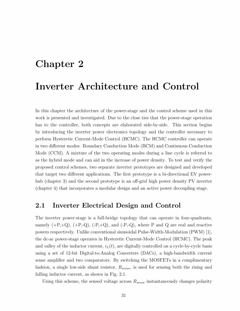
Chapter 2
Inverter Architecture and Control
In this chapter the architecture of the power-stage and the control scheme used in this
work is presented and investigated. Due to the close ties that the power-stage operation
has to the controller, both concepts are elaborated side-by-side. This section begins
by introducing the inverter power electronics topology and the controller necessary to
perform Hysteretic Current-Mode Control (HCMC). The HCMC controller can operate
in two different modes: Boundary Conduction Mode (BCM) and Continuous Conduction
Mode (CCM). A mixture of the two operating modes during a line cycle is referred to
as the hybrid mode and can aid in the increase of power density. To test and verify the
proposed control schemes, two separate inverter prototypes are designed and developed
that target two different applications. The first prototype is a bi-directional EV power-
hub (chapter 3) and the second prototype is an off-grid high power density PV inverter
(chapter 4) that incorporates a modular design and an active power decoupling stage.
2.1 Inverter Electrical Design and Control
The inverter power-stage is a full-bridge topology that can operate in four-quadrants,
namely (+P,+Q), (+P,-Q), (-P,+Q), and (-P,-Q), where P and Q are real and reactive
powers respectively. Unlike conventional sinusoidal Pulse-Width-Modulation (PWM) [1],
the dc-ac power-stage operates in Hysteretic Current-Mode Control (HCMC). The peak
and valley of the inductor current, iL(t), are digitally controlled on a cycle-by-cycle basis
using a set of 12-bit Digital-to-Analog Converters (DACs), a high-bandwidth current
sense amplifier and two comparators. By switching the MOSFETs in a complimentary
fashion, a single low-side shunt resistor, Rsense, is used for sensing both the rising and
falling inductor current, as shown in Fig. 2.1.
Using this scheme, the sensed voltage across Rsense instantaneously changes polarity
31

Chapter 2. Inverter Architecture and Control 32
as one set of switches commutates. A digital controller is used for precise current-control
and a 60 Hz synchronization pulse is used for grid phase locking. The control logic
contains an active-low set-reset flip-flop a with built in blanking time module to eliminate
false current limit triggers. This module also contains auxiliary safety features including a
precise timer to prevent unwanted latch-up of the MOSFETs in the ON state. The digital
current modulator block contains a precision sine Look Up Table (LUT) and generates
the necessary peak and valley digital current limits. This module is also responsible for
transitioning between BCM and hybrid HCMC operating modes depending on the load
power-level.
iL(t)
iR
Rsense
Vin
+
-
Cin
SiC MOSFETs
DigitalCurrent
Modulator
D/A
D/A
Control
Logic
Current Loop
SyncGrid Synchronization
Voltage loop current scaling
Mode selection
A/D
vsense
900V
Rload
Vac
OR
Voltage loop/Zero crossing
detection
EMIfilter
DTControl
HS1LS1HS2LS2
HS1
LS1
HS2
LS2
Vin
Sub-inverter
Controller
A/DPolarity
V1
V2
+-
Figure 2.1: Architecture of the full-bridge inverter topology and hysteretic current-mode
controller.
The digital current reference is scaled by the controller as part of the outer voltage
loop. A pre-calibrated digital feed-forward scheme can be used to precisely set the dead-
times with 5 ns resolution in all operating modes in order to minimize the MOSFET
switching losses under all conditions. While the SiC-based inverter can easily operate
above 500 kHz, the frequency is limited to 300 kHz for optimal efficiency. Due to the
utilization of HCMC, slope compensation is not necessary.
2.1.1 BCM, CCM, and Hybrid Operating Modes
The inverter operates in two possible modes throughout the ac line-cycle: 1) BCM or
2) CCM, as shown by the current waveform in Fig. 2.1. The combination of these two
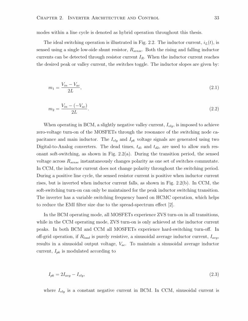
Chapter 2. Inverter Architecture and Control 33
modes within a line cycle is denoted as hybrid operation throughout this thesis.
The ideal switching operation is illustrated in Fig. 2.2. The inductor current, iL(t), is
sensed using a single low-side shunt resistor, Rsense. Both the rising and falling inductor
currents can be detected through resistor current IR. When the inductor current reaches
the desired peak or valley current, the switches toggle. The inductor slopes are given by:
m1 =Vin − Vac
2L, (2.1)
m2 =Vin − (−Vac)
2L. (2.2)
When operating in BCM, a slightly negative valley current, Ivly, is imposed to achieve
zero-voltage turn-on of the MOSFETs through the resonance of the switching node ca-
pacitance and main inductor. The Ivly and Ipk voltage signals are generated using two
Digital-to-Analog converters. The dead times, td1 and td2, are used to allow such res-
onant soft-switching, as shown in Fig. 2.2(a). During the transition period, the sensed
voltage across Rsense instantaneously changes polarity as one set of switches commutate.
In CCM, the inductor current does not change polarity throughout the switching period.
During a positive line cycle, the sensed resistor current is positive when inductor current
rises, but is inverted when inductor current falls, as shown in Fig. 2.2(b). In CCM, the
soft-switching turn-on can only be maintained for the peak inductor switching transition.
The inverter has a variable switching frequency based on HCMC operation, which helps
to reduce the EMI filter size due to the spread-spectrum effect [2].
In the BCM operating mode, all MOSFETs experience ZVS turn-on in all transitions,
while in the CCM operating mode, ZVS turn-on is only achieved at the inductor current
peaks. In both BCM and CCM all MOSFETs experience hard-switching turn-off. In
off-grid operation, if Rload is purely resistive, a sinusoidal average inductor current, Iavg,
results in a sinusoidal output voltage, Vac. To maintain a sinusoidal average inductor
current, Ipk is modulated according to
Ipk = 2Iavg − Ivly, (2.3)
where Ivly is a constant negative current in BCM. In CCM, sinusoidal current is

Chapter 2. Inverter Architecture and Control 34
IL
IR
0
+Ipk
+Ivly
-Ivly
-I pk
HS1
LS1
HS2
LS2
0
+Vbus Vx1 Vx2
td1 td1
td2
Iavgm1 m2
(a)
HS1
LS1
HS2
LS2
IL
IR
0
+Ipk
+Ivly
-I vly
-I pk
0
+Vbus Vx1 Vx2
td1
td1
t d2
Iavg hard switchingsoft switchingΔI
(b)
Figure 2.2: Detailed waveforms of the HCMC controller operation in (a) BCM and (b)CCM.
maintained by setting a fixed ripple current, ∆I, around Iavg such that
Ipk = Iavg +∆I
2, (2.4)
and
Ivly = Iavg −∆I
2, (2.5)
as shown in Fig. 2.2(b).
The inverter is controlled in two possible modes depending on the desired output
averaged RMS current. For lower output current levels, the converter operates in BCM
throughout the ac line-cycle, as shown in Fig. 2.3(a), and for higher output current levels,
the converter switches into hybrid mode, as shown in Fig. 2.3(b). During the zero crossing
regions, the Ipk and Ivly current limits are set to the same constant value such that the
inductor has zero average current.
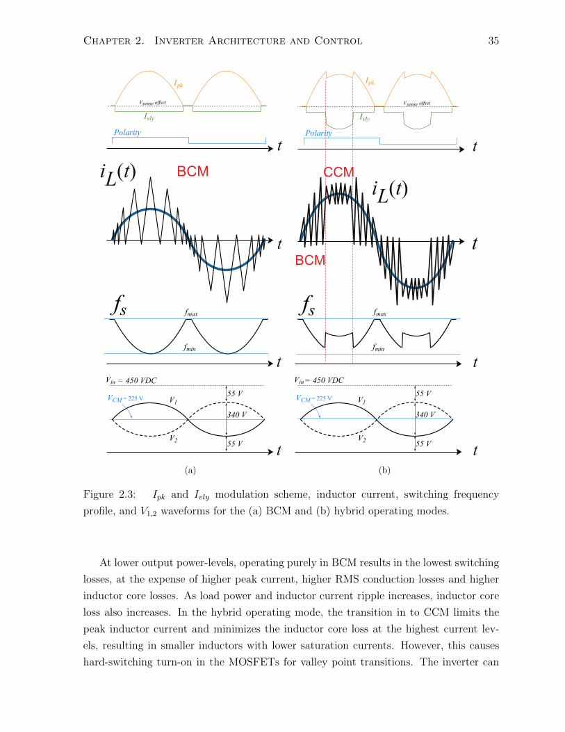
Chapter 2. Inverter Architecture and Control 35
BCMiL(t)
t
fsfmin
fmax
t
t
VCM = 225 V V1
V2
Vin
340 V
55 V
55 V
t
Ipk
Ivly
Polarity
Vsense offset
= 450 VDC
(a)
BCM
CCM
iL(t)
t
fsfmin
fmax
t
t
VCM = 225 V V1
V2
Vin
340 V
55 V
55 V
tPolarity
Vsense offset
Ipk
Ivly
= 450 VDC
(b)
Figure 2.3: Ipk and Ivly modulation scheme, inductor current, switching frequency
profile, and V1,2 waveforms for the (a) BCM and (b) hybrid operating modes.
At lower output power-levels, operating purely in BCM results in the lowest switching
losses, at the expense of higher peak current, higher RMS conduction losses and higher
inductor core losses. As load power and inductor current ripple increases, inductor core
loss also increases. In the hybrid operating mode, the transition in to CCM limits the
peak inductor current and minimizes the inductor core loss at the highest current lev-
els, resulting in smaller inductors with lower saturation currents. However, this causes
hard-switching turn-on in the MOSFETs for valley point transitions. The inverter can
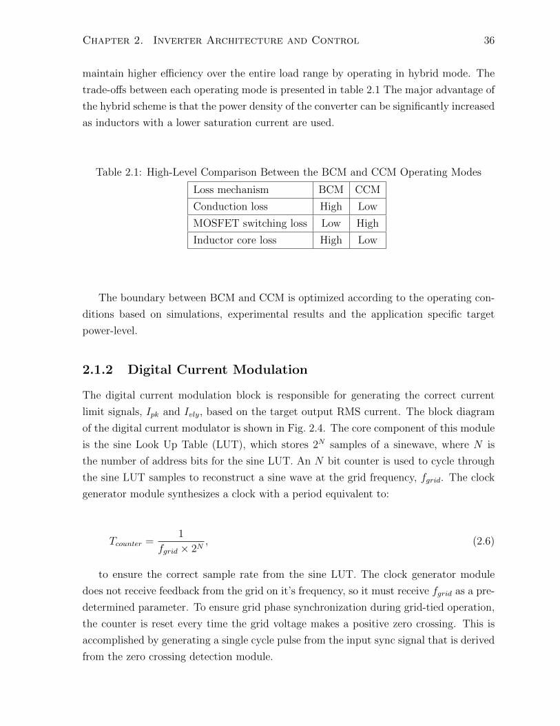
Chapter 2. Inverter Architecture and Control 36
maintain higher efficiency over the entire load range by operating in hybrid mode. The
trade-offs between each operating mode is presented in table 2.1 The major advantage of
the hybrid scheme is that the power density of the converter can be significantly increased
as inductors with a lower saturation current are used.
Table 2.1: High-Level Comparison Between the BCM and CCM Operating Modes
Loss mechanism BCM CCM
Conduction loss High Low
MOSFET switching loss Low High
Inductor core loss High Low
The boundary between BCM and CCM is optimized according to the operating con-
ditions based on simulations, experimental results and the application specific target
power-level.
2.1.2 Digital Current Modulation
The digital current modulation block is responsible for generating the correct current
limit signals, Ipk and Ivly, based on the target output RMS current. The block diagram
of the digital current modulator is shown in Fig. 2.4. The core component of this module
is the sine Look Up Table (LUT), which stores 2N samples of a sinewave, where N is
the number of address bits for the sine LUT. An N bit counter is used to cycle through
the sine LUT samples to reconstruct a sine wave at the grid frequency, fgrid. The clock
generator module synthesizes a clock with a period equivalent to:
Tcounter =1
fgrid × 2N, (2.6)
to ensure the correct sample rate from the sine LUT. The clock generator module
does not receive feedback from the grid on it’s frequency, so it must receive fgrid as a pre-
determined parameter. To ensure grid phase synchronization during grid-tied operation,
the counter is reset every time the grid voltage makes a positive zero crossing. This is
accomplished by generating a single cycle pulse from the input sync signal that is derived
from the zero crossing detection module.

Chapter 2. Inverter Architecture and Control 37
Clockgenerator
N bitcounter
Single-shotpulse generator
50 MHz
Grid frequencyselector
50 Hz or 60 Hz
Sync signal(polarity)
Scaling factorfrom voltage loop
Sensor offset
BCMIpk, Ivly
generator
CCMIpk, Ivly
generator
Zerocrossingregion
Ipk, Ivlyto DACs
2-to-1mux
BCM/Hybridmode boundary
Sine LUT
Sample 0Sample 1Sample 2Sample 3
.
.
.
.
.
.
.
.Sample 2N
N
1/60 Hz
Figure 2.4: Block diagram of the digital current modulator
The streaming samples from the sine LUT are scaled by the voltage loop and a
constant offset is added to match with the current sensor biasing. The resultant signal
is fed in to the BCM and CCM current limit generators which recreate the required Ipk
and Ivly signals for correct HCMC operation based on equations 2.3, 2.4, and 2.5. The
scaled sine LUT output is compared against a predetermined and optimized boundary
for switching between BCM or CCM mode to select the correct operating mode for the
inverter using a 2-to-1 multiplexer. At low power-levels the comparator outputs logic zero
at all times and this results in the BCM operating mode. At higher power-levels, the
comparator outputs logic one when the scaled sine wave peaks above the mode selection
boundary pushing the inverter into CCM which results in the hybrid operating mode.
To prevent very high switching frequencies near the current zero crossings, Ipk and Ivly
are clipped, before being transferred to the DACs.
2.1.3 Control Logic
The control logic contains a set-reset flip flop with active-low inputs followed by a blanking
time module to prevent inductor current ringing to affect the HCMC operation after a
switching event, as shown in Fig. 2.5. The inductor ringing is caused by the resonance
of the PCB trace inductance with the phase node capacitance. During the negative half
of the ac line cycle, the Q and Q signals are switched according to the polarity signal
and this swaps the MOSFET commutation order. To protect the inverter from unwanted
MOSFET latch up, an over-current protection module is designed to time the turn-on
duration of the MOSFETs and trip the gating signals in case a MOSFET remains ON
longer than expected.
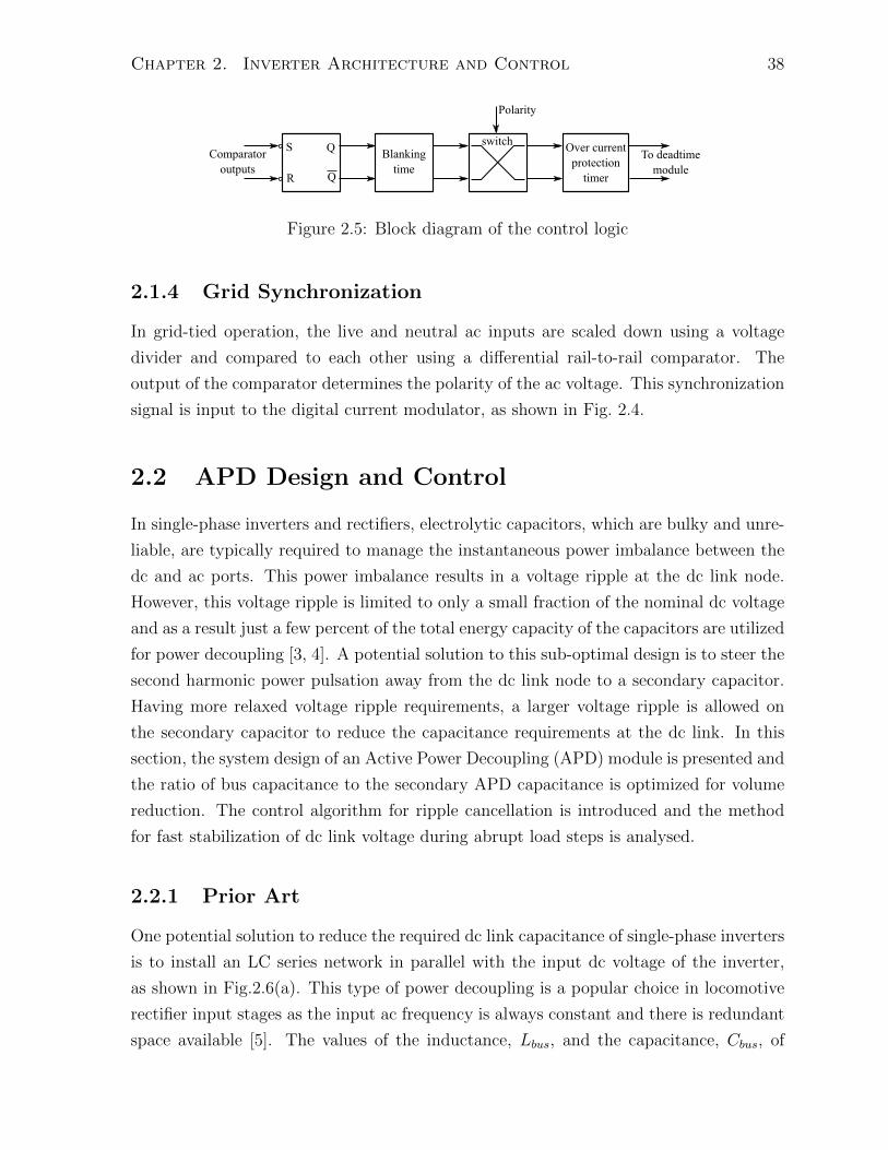
Chapter 2. Inverter Architecture and Control 38
Blankingtime
Over currentprotection
timer
S
R
Q
Q
Comparatoroutputs
To deadtimemodule
switch
Polarity
Figure 2.5: Block diagram of the control logic
2.1.4 Grid Synchronization
In grid-tied operation, the live and neutral ac inputs are scaled down using a voltage
divider and compared to each other using a differential rail-to-rail comparator. The
output of the comparator determines the polarity of the ac voltage. This synchronization
signal is input to the digital current modulator, as shown in Fig. 2.4.
2.2 APD Design and Control
In single-phase inverters and rectifiers, electrolytic capacitors, which are bulky and unre-
liable, are typically required to manage the instantaneous power imbalance between the
dc and ac ports. This power imbalance results in a voltage ripple at the dc link node.
However, this voltage ripple is limited to only a small fraction of the nominal dc voltage
and as a result just a few percent of the total energy capacity of the capacitors are utilized
for power decoupling [3, 4]. A potential solution to this sub-optimal design is to steer the
second harmonic power pulsation away from the dc link node to a secondary capacitor.
Having more relaxed voltage ripple requirements, a larger voltage ripple is allowed on
the secondary capacitor to reduce the capacitance requirements at the dc link. In this
section, the system design of an Active Power Decoupling (APD) module is presented and
the ratio of bus capacitance to the secondary APD capacitance is optimized for volume
reduction. The control algorithm for ripple cancellation is introduced and the method
for fast stabilization of dc link voltage during abrupt load steps is analysed.
2.2.1 Prior Art
One potential solution to reduce the required dc link capacitance of single-phase inverters
is to install an LC series network in parallel with the input dc voltage of the inverter,
as shown in Fig.2.6(a). This type of power decoupling is a popular choice in locomotive
rectifier input stages as the input ac frequency is always constant and there is redundant
space available [5]. The values of the inductance, Lbus, and the capacitance, Cbus, of
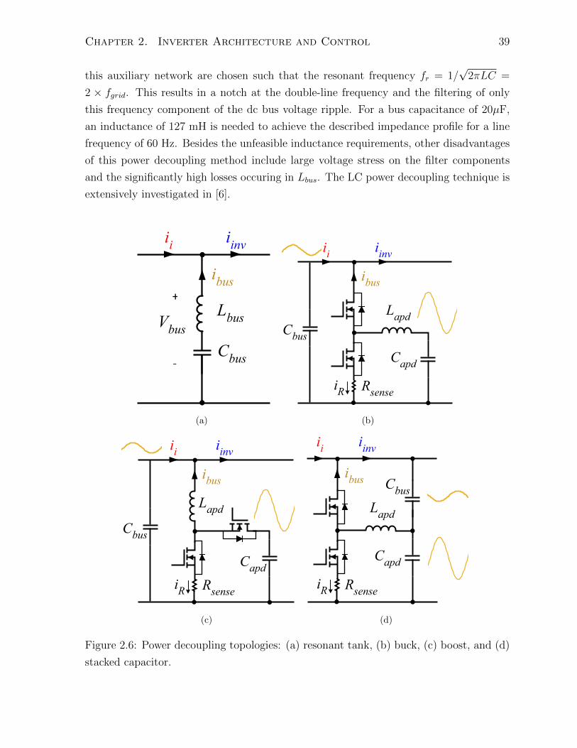
Chapter 2. Inverter Architecture and Control 39
this auxiliary network are chosen such that the resonant frequency fr = 1/√
2πLC =
2 × fgrid. This results in a notch at the double-line frequency and the filtering of only
this frequency component of the dc bus voltage ripple. For a bus capacitance of 20µF,
an inductance of 127 mH is needed to achieve the described impedance profile for a line
frequency of 60 Hz. Besides the unfeasible inductance requirements, other disadvantages
of this power decoupling method include large voltage stress on the filter components
and the significantly high losses occuring in Lbus. The LC power decoupling technique is
extensively investigated in [6].
Cbus
LbusV
bus
ii
iinv
ibus
(a)
ii
iinv
ibus
Lapd
Capd
Rsense
Cbus
iR
(b)
ii
iinv
ibus
Lapd
Capd
Rsense
Cbus
iR
(c)
ii
iinv
ibus
Lapd
Capd
Rsense
Cbus
iR
(d)
Figure 2.6: Power decoupling topologies: (a) resonant tank, (b) buck, (c) boost, and (d)
stacked capacitor.

Chapter 2. Inverter Architecture and Control 40
A more effective way of steering the pulsating power away from the dc bus is to use
an active circuit to charge and discharge a secondary capacitor, Capd, during every bus
voltage ripple cycle with a much higher voltage ripple than Cbus. One popular circuit
is shown in Fig. 2.6(b) which is commonly referred to as the buck APD topology [6].
This topology is extensively studied in the literature [7–9] and the minimum required
secondary capacitance is theoretically derived to be
Capd,min =2Sb
ωV 2dc
, (2.7)
where Sb is the apparent power of the ac load and ω is the line frequency, as analyzed
in [10].
Another prevalent APD circuit is the boost topology, as shown in Fig. 2.6(c), which
has higher voltage stress on the APD MOSFETs [11]. A half-bridge stacked capacitor
APD topology is analyzed in [9, 12], where two capacitors are stacked in series and
the midpoint is connected to the half-bridge phase node through a small inductor, as
demonstrated in Fig. 2.6(d). The main advantage of this topology is that both Cbus
and Capd are directly decoupling the dc bus and the half-bridge is steering the pulsating
energy into Capd at the same time. The minimum required APD capacitance is
Capd,min =4Sb
ωV 2dc
, (2.8)
as derived in [9], which shows a 2× increase in capacitance as compared to the buck
APD topology. In the active APD topologies, the current sense resistor, Rsense, is used
for controlling the current through Lapd using current-mode control. Due to the location
of Rsense, only the falling slope of iLapdis detectable and the controller has no control over
the location of the peaks. This results in inaccurate timing of the current peaks which
can lead to non-sinusoidal power transfer from the dc bus. Moreover, the inaccuracies
present in this control scheme results in the loss of soft-switching for the MOSFETs
during the negative portion of the APD current cycle.
2.2.2 Full-Bridge Differential Active Power Decoupling
Having addressed some of the key disadvantages of prevalent APD topologies, the full-
bridge APD architecture was selected for the inverter design which allows the inverter
circuit design to be re-utilized for the APD phase, reducing the extra complexities asso-
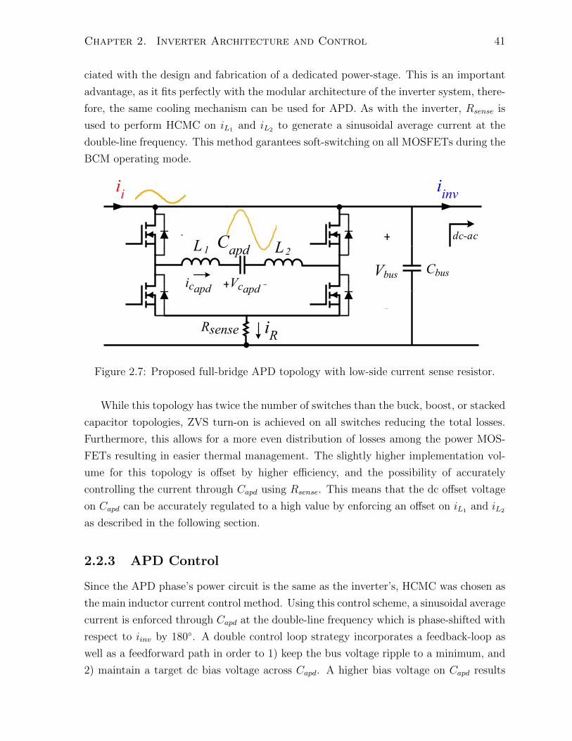
Chapter 2. Inverter Architecture and Control 41
ciated with the design and fabrication of a dedicated power-stage. This is an important
advantage, as it fits perfectly with the modular architecture of the inverter system, there-
fore, the same cooling mechanism can be used for APD. As with the inverter, Rsense is
used to perform HCMC on iL1 and iL2 to generate a sinusoidal average current at the
double-line frequency. This method garantees soft-switching on all MOSFETs during the
BCM operating mode.
ii
iinv
iR
Capd
Vcapdicapd
Figure 2.7: Proposed full-bridge APD topology with low-side current sense resistor.
While this topology has twice the number of switches than the buck, boost, or stacked
capacitor topologies, ZVS turn-on is achieved on all switches reducing the total losses.
Furthermore, this allows for a more even distribution of losses among the power MOS-
FETs resulting in easier thermal management. The slightly higher implementation vol-
ume for this topology is offset by higher efficiency, and the possibility of accurately
controlling the current through Capd using Rsense. This means that the dc offset voltage
on Capd can be accurately regulated to a high value by enforcing an offset on iL1 and iL2
as described in the following section.
2.2.3 APD Control
Since the APD phase’s power circuit is the same as the inverter’s, HCMC was chosen as
the main inductor current control method. Using this control scheme, a sinusoidal average
current is enforced through Capd at the double-line frequency which is phase-shifted with
respect to iinv by 180. A double control loop strategy incorporates a feedback-loop as
well as a feedforward path in order to 1) keep the bus voltage ripple to a minimum, and
2) maintain a target dc bias voltage across Capd. A higher bias voltage on Capd results
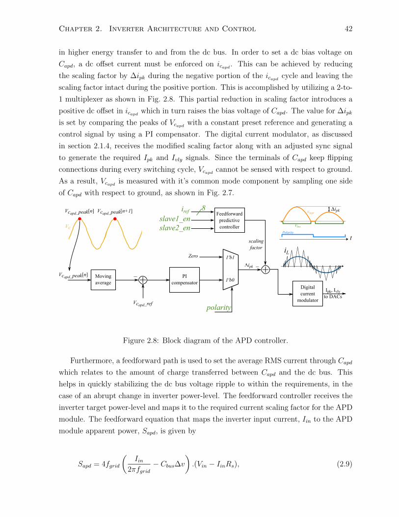
Chapter 2. Inverter Architecture and Control 42
in higher energy transfer to and from the dc bus. In order to set a dc bias voltage on
Capd, a dc offset current must be enforced on icapd . This can be achieved by reducing
the scaling factor by ∆ipk during the negative portion of the icapd cycle and leaving the
scaling factor intact during the positive portion. This is accomplished by utilizing a 2-to-
1 multiplexer as shown in Fig. 2.8. This partial reduction in scaling factor introduces a
positive dc offset in icapd which in turn raises the bias voltage of Capd. The value for ∆ipk
is set by comparing the peaks of Vcapd with a constant preset reference and generating a
control signal by using a PI compensator. The digital current modulator, as discussed
in section 2.1.4, receives the modified scaling factor along with an adjusted sync signal
to generate the required Ipk and Ivly signals. Since the terminals of Capd keep flipping
connections during every switching cycle, Vcapd cannot be sensed with respect to ground.
As a result, Vcapd is measured with it’s common mode component by sampling one side
of Capd with respect to ground, as shown in Fig. 2.7.
PIcompensator
Feedforwardpredictivecontroller
irefslave1_en
slave2_en
8
Digitalcurrent
modulator
Movingaverage
Vcapd_ref
Zero
Vc
Vcapd_peak[n] Vcapd_peak[n+1]
polarity
1'b0
1'b1
t
Vhigh
Vlow
Polarity
iL
ipk
ipk
scaling
factor
Ipk, Ivlyto DACs
Vcapd_peak[n]
Figure 2.8: Block diagram of the APD controller.
Furthermore, a feedforward path is used to set the average RMS current through Capd
which relates to the amount of charge transferred between Capd and the dc bus. This
helps in quickly stabilizing the dc bus voltage ripple to within the requirements, in the
case of an abrupt change in inverter power-level. The feedforward controller receives the
inverter target power-level and maps it to the required current scaling factor for the APD
module. The feedforward equation that maps the inverter input current, Iin to the APD
module apparent power, Sapd, is given by
Sapd = 4fgrid
(Iin
2πfgrid− Cbus∆v
).(Vin − IinRs), (2.9)
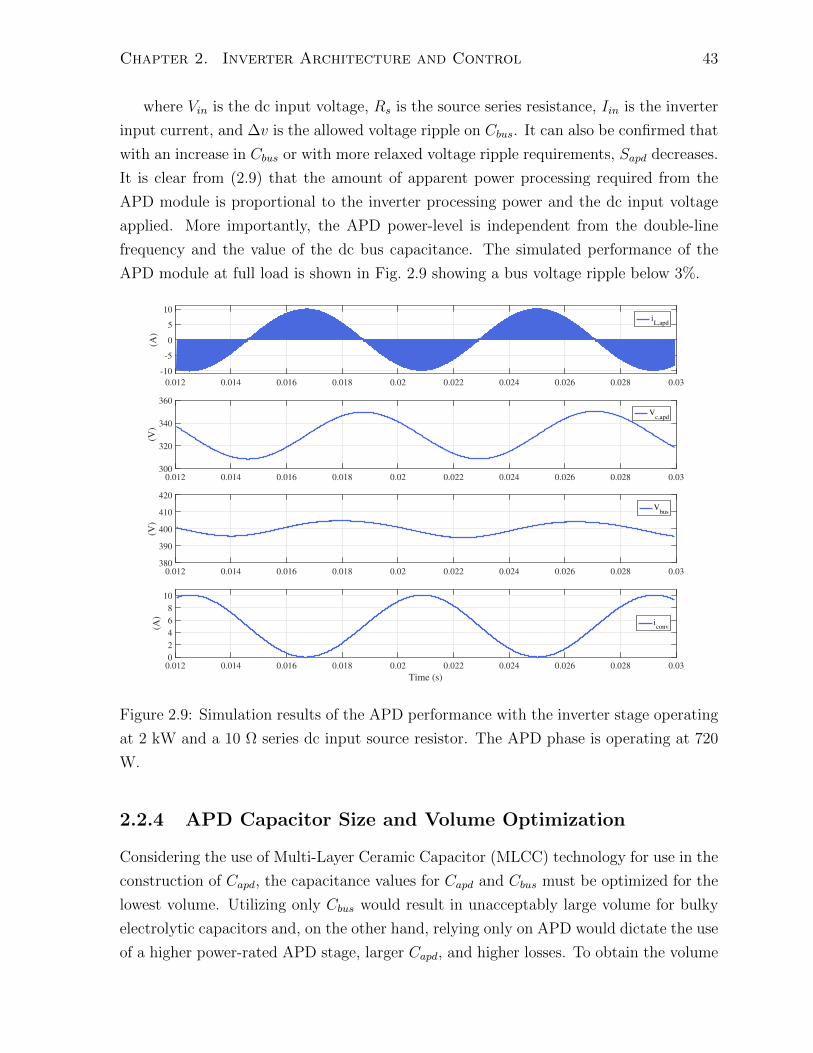
Chapter 2. Inverter Architecture and Control 43
where Vin is the dc input voltage, Rs is the source series resistance, Iin is the inverter
input current, and ∆v is the allowed voltage ripple on Cbus. It can also be confirmed that
with an increase in Cbus or with more relaxed voltage ripple requirements, Sapd decreases.
It is clear from (2.9) that the amount of apparent power processing required from the
APD module is proportional to the inverter processing power and the dc input voltage
applied. More importantly, the APD power-level is independent from the double-line
frequency and the value of the dc bus capacitance. The simulated performance of the
APD module at full load is shown in Fig. 2.9 showing a bus voltage ripple below 3%.
0.012 0.014 0.016 0.018 0.02 0.022 0.024 0.026 0.028 0.03
-10
-5
0
5
10
(A)
iL,apd
0.012 0.014 0.016 0.018 0.02 0.022 0.024 0.026 0.028 0.03300
320
340
360
(V)
Vc,apd
0.012 0.014 0.016 0.018 0.02 0.022 0.024 0.026 0.028 0.03380
390
400
410
420
(V)
Vbus
0.012 0.014 0.016 0.018 0.02 0.022 0.024 0.026 0.028 0.03
Time (s)
0
2
4
6
8
10
(A)
iconv
Figure 2.9: Simulation results of the APD performance with the inverter stage operating
at 2 kW and a 10 Ω series dc input source resistor. The APD phase is operating at 720
W.
2.2.4 APD Capacitor Size and Volume Optimization
Considering the use of Multi-Layer Ceramic Capacitor (MLCC) technology for use in the
construction of Capd, the capacitance values for Capd and Cbus must be optimized for the
lowest volume. Utilizing only Cbus would result in unacceptably large volume for bulky
electrolytic capacitors and, on the other hand, relying only on APD would dictate the use
of a higher power-rated APD stage, larger Capd, and higher losses. To obtain the volume

Chapter 2. Inverter Architecture and Control 44
optimal ratio of Capd/Cbus, a series of PLECS simulations were conducted, assuming a
2 kW inverter. The value of Capd was swept from 30 µF to 270 µF while keeping the APD
RMS current-level at 4 A. At every simulation run, the value for Cbus was determined
for meeting the 3% bus voltage ripple requirements. The maximum possible vc ref was
set while keeping the voltage ripple on Capd in mind. Considering the use of a network of
2.2 µF 450 V MLCC capacitors from TDK [13] for the construction of Capd, an optimal
total capacitor volume of 17680 mm3 was obtained with Capd and Cbus being 124 µF
and 120 µF respectively, as shown in Fig. 2.10. At the maximum inverter power-level, a
dc bias of 342 V was achievable for Vcapd with a peak-to-peak ripple of 42 Vpk−pk which
results in 2.87% of bus voltage ripple.
0 50 100 150 200 250 300APD capacitance (uF)
1.5
2
2.5
3
3.5
4
4.5
5
Tota
l cap
acito
r vol
ume
requ
ired
(mm
3 )
104
200
220
240
260
280
300
320
340
360
380
Ave
rage
APD
cap
acito
r vol
tage
(V)
Volume optimalcapacitance
Figure 2.10: Total system capacitor volume required versus the amount of APD capac-
itance and the maximum attainable average APD capacitor voltage. The optimal APD
capacitance range is 100-150 µF.
2.3 Chapter Summary
In this chapter, the system architecture for a full-bridge inverter utilizing a novel BCM/hybrid
current-mode control scheme is introduced and analysed. The hybrid scheme is defined
to be the combination of BCM and CCM during an ac line-cycle to limit the peak in-

Chapter 2. Inverter Architecture and Control 45
ductor current. This operating mode reduces the saturation current requirements for the
inductors and hence, smaller inductors become feasible. The use of a single low-side cur-
rent sense resistor is also another benefit of this architecture as it reduces cost and error
when compared with hall-effect or high-side current sensing schemes. Finally, the idea
behind Active Power Decoupling (APD) is provided and a literature review is presented,
covering different APD design approaches. The full-bridge APD topology is selected as
the most suitable converter for the purpose of the off-grid PV inverter project due to
lower switching losses and similarities to the inverter topology. The chapter concludes
by providing a discussion on the volume optimization strategy for Capd and Cbus which
involved a series of simulations to obtain the optimal Capd to Cbus ratio.

References
[1] S. R. Bowes, “New sinusoidal pulsewidth-modulated invertor,” Electrical Engineers,
Proceedings of the Institution of, vol. 122, no. 11, pp. 1279–1285, November 1975.
[2] S. Y. Oh, Y. G. Jung, S. H. Yang, and Y. C. Lim, “Harmonic-spectrum spreading
effects of two-phase random centered distribution pwm (dzrcd) scheme with dual
zero vectors,” IEEE Transactions on Industrial Electronics, vol. 56, no. 8, pp. 3013–
3020, Aug 2009.
[3] Y. Sun, Y. Liu, M. Su, W. Xiong, and J. Yang, “Review of active power decou-
pling topologies in single-phase systems,” IEEE Transactions on Power Electronics,
vol. 31, no. 7, pp. 4778–4794, July 2016.
[4] G. C. Christidis, A. C. Kyritsis, N. P. Papanikolaou, and E. C. Tatakis, “Investiga-
tion of parallel active filters; limitations for power decoupling on single-stage/single-
phase microinverters,” IEEE Journal of Emerging and Selected Topics in Power
Electronics, vol. 4, no. 3, pp. 1096–1106, Sept 2016.
[5] G. Bocchetti, M. Carpita, G. Giannini, and S. Tenconi, “Line filter for high power
inverter locomotive using active circuit for harmonic reduction,” in 1993 Fifth Eu-
ropean Conference on Power Electronics and Applications, Sept 1993, pp. 267–271
vol.8.
[6] D. Neumayr, D. Bortis, and J. W. Kolar, “Ultra-compact power pulsation buffer
for single-phase dc/ac converter systems,” in 2016 IEEE 8th International Power
Electronics and Motion Control Conference (IPEMC-ECCE Asia), May 2016, pp.
2732–2741.
[7] Z. Qin, Y. Tang, P. C. Loh, and F. Blaabjerg, “Benchmark of ac and dc active power
decoupling circuits for second-order harmonic mitigation in kw-scale single-phase
inverters,” in 2015 IEEE Energy Conversion Congress and Exposition (ECCE), Sept
2015, pp. 2514–2521.
46
REFERENCES 47
[8] H. Li, K. Zhang, H. Zhao, S. Fan, and J. Xiong, “Active power decoupling for
high-power single-phase pwm rectifiers,” IEEE Transactions on Power Electronics,
vol. 28, no. 3, pp. 1308–1319, March 2013.
[9] Y. Tang, F. Blaabjerg, P. C. Loh, C. Jin, and P. Wang, “Decoupling of fluctuating
power in single-phase systems through a symmetrical half-bridge circuit,” IEEE
Transactions on Power Electronics, vol. 30, no. 4, pp. 1855–1865, April 2015.
[10] R. Wang, F. Wang, D. Boroyevich, R. Burgos, R. Lai, P. Ning, and K. Rajashekara,
“A high power density single-phase pwm rectifier with active ripple energy storage,”
IEEE Transactions on Power Electronics, vol. 26, no. 5, pp. 1430–1443, May 2011.
[11] A. C. Kyritsis, N. P. Papanikolaou, and E. C. Tatakis, “A novel parallel active filter
for current pulsation smoothing on single stage grid-connected ac-pv modules,” in
2007 European Conference on Power Electronics and Applications, Sept 2007, pp.
1–10.
[12] S. Chung, M. Nasr, D. Guirguis, M. Otsuka, S. Poshtkouhi, D. K. W. Li, V. Pala-
niappan, D. Romero, C. Amon, R. Orr, and O. Trescases, “Thermal and electrical
co-design of a modular high-density single-phase inverter using wide-bandgap de-
vices,” in 2016 IEEE Applied Power Electronics Conference and Exposition (APEC),
March 2016, pp. 1350–1357.
[13] “Multilayer ceramic chip capacitors,” TDK Datasheet, available
https://product.tdk.com/info/en/catalog/datasheets/mlcc commercial midvoltage en.pdf.

Chapter 3
EV Power-Hub
Details regarding the power-stage implementation, component selection, inductor and
EMI filter design, auxiliary power-supply, and the thermal and mechanical system of the
EV power-hub is covered in this chapter. Utilizing the extracted loss data from detailed
Cadence simulations, the thermal and mechanical systems were co-designed to ensure safe
operation of the semiconductors and magnetics. This project is expected to be published
in March 2018 and the prepublication digest has been submitted and accepted [1].
3.1 Implementation
The main PCB for the EV power-hub, as shown in Fig. 3.1, is divided into two sections:
1) the dc-ac inverter, and 2) a Dual-Active-Bridge (DAB) dc-dc converter, which is used
for isolation, battery current control, and voltage step up/down. The DAB converter is
outside the scope of this thesis. The dc-ac section contains the power-stage with isolated
gate drivers, main power inductors, EMI filter, and ac side input protection. The power-
hub contains a central FPGA that provides the necessary gating signals for both the
dc-ac and dc-dc converters. The PCB contains four layers with 4 oz/ft2 copper weight.
3.1.1 Power-Stage
Each switch in the power-hub, as is shown in Fig. 3.1, is implemented using two paralleled
900 V, 35 A, 65 mΩ, SiC SMD devices. The two high-side MOSFET pairs are placed
on the top side of the PCB and the two low-side MOSFET pairs are placed directly
underneath the high-side MOSFETs on the bottom side of the PCB. This results in the
least PCB trace inductance due to the smaller loop area as opposed to having all eight
MOSFETs on the same side. The four high side MOSFETs are driven with a dual output
48

Chapter 3. EV Power-Hub 49
6 A isolated gate driver and the four low-side MOSFETs are driven by another gate driver
placed on the bottom side of the PCB. Each MOSFET has a dedicated gate resistor and
each MOSFET pair has a common gate resistor. Four 1 µF, 500V ceramic capacitors are
used for local power decoupling of the full-bridge power-stage which helps in reducing the
current ringing on the high di/dt loop. Seven 120 µF, 600 V electrolytic capacitors are
installed on the dc link to decouple the dc-ac and dc-dc stages. Active Power Decoupling
(APD), as discussed in section 2.2, is not implemented in the EV power-hub.
Inverter DAB converter
Inductors
Paralleled SiC MOSFETs
Fuses
Relay
DC bus capacitors
EMI filter
AC terminal
DC terminal
FPGA and digital isolators
Isolatedgate driver
HS1 HS2
Figure 3.1: Top side view of the EV power-hub PCB containing the inverter and a DAB
dc-dc converter. The DAB converter is outside the scope of this thesis.
The gate drive circuitry for every paralleled MOSFET pair is shown in Fig. 3.2. A
common gate resistance, Rg1, is utilized for limiting the gate current ringing followed by
two individual gate resistors, Rg2. The purpose of splitting the total gate resistance in
to Rg1 and Rg2 is to be able to compensate for the potential mismatches in MOSFET
turn-on and turn-off behaviour by modifying each Rg2 if needed. Due to the inevitable
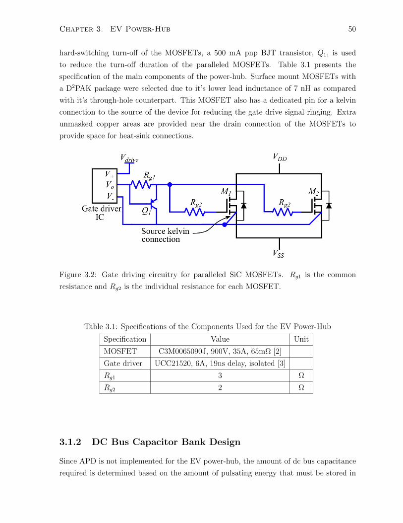
Chapter 3. EV Power-Hub 50
hard-switching turn-off of the MOSFETs, a 500 mA pnp BJT transistor, Q1, is used
to reduce the turn-off duration of the paralleled MOSFETs. Table 3.1 presents the
specification of the main components of the power-hub. Surface mount MOSFETs with
a D2PAK package were selected due to it’s lower lead inductance of 7 nH as compared
with it’s through-hole counterpart. This MOSFET also has a dedicated pin for a kelvin
connection to the source of the device for reducing the gate drive signal ringing. Extra
unmasked copper areas are provided near the drain connection of the MOSFETs to
provide space for heat-sink connections.
Figure 3.2: Gate driving circuitry for paralleled SiC MOSFETs. Rg1 is the common
resistance and Rg2 is the individual resistance for each MOSFET.
Table 3.1: Specifications of the Components Used for the EV Power-Hub
Specification Value Unit
MOSFET C3M0065090J, 900V, 35A, 65mΩ [2]
Gate driver UCC21520, 6A, 19ns delay, isolated [3]
Rg1 3 Ω
Rg2 2 Ω
3.1.2 DC Bus Capacitor Bank Design
Since APD is not implemented for the EV power-hub, the amount of dc bus capacitance
required is determined based on the amount of pulsating energy that must be stored in
Chapter 3. EV Power-Hub 51
the capacitors. The required size of the bus capacitance is given by:
C =Pdc
2πfVdc∆v(3.1)
where f is the line frequency, Pdc is the inverter rated power, Vdc is the average dc
bus voltage, and ∆v is the maximum allowable peak-to-peak bus voltage ripple [4, 5].
Using a Pdc of 6.6 kW, a Vdc of 450 V, and a ∆v of 40V, a bus capacitance of 970 µF is
needed according to (3.1). The 970 µF capacitor bank is constructed with seven 120 µF,
600 V capacitors to spread out the volume requirement and reduce the overall height of
the capacitor bank.
3.1.3 Inductors
In order to operate the converter with a maximum switching frequency of 250 kHz and
a peak grid current of 37.5 A, 50 µH line inductance rated at 45 A peak is needed. To
ensure both switching nodes of the full-bridge converter see the same line impedance, the
total 50 µH line inductance is split into two 25 µH inductors connected to each switching
node. This also helps in spreading out the total power loss over a larger surface area. The
inductors are custom made with AWG 9 litz wire and the ETD44 core size was tentatively
chosen. Considering a Bsat of 0.32 T for the N97 ferrite material, the required number
of turns, N , is given by:
N =L∆Imax
∆BmaxAe
(3.2)
where ∆Bmax is the maximum flux density swing, ∆Imax is the peak inductor current,
and Ae is the cross-sectional area of the core [6]. To prevent excessive core loss, ∆Bmax
is set to 0.3 T which is slightly less than Bsat = 0.32 T. The air gap length, `g, required
to meet the saturation current requirement is calculated using:
`g = µ0N2Ag
L(3.3)
where µ0 is the permeability of free space and Ag is the gap cross-sectional area. This
results in an air gap of 0.3cm. Details regarding the designed inductor and the ferrite
material are provided in table 3.2.

Chapter 3. EV Power-Hub 52
Table 3.2: Specifications for the Power-Hub Inductors. Two 25 µH Inductors are Used
for the Line Inductance
Specification Value Unit
Inductance 25 µH
Saturation current, Isat 45 A
Number of turns, N 15 turns
Gap length 3 mm
Core area, Ae 1.73 cm2
Litz wire diameter 3 mm
The windings are kept far away from the air gap to prevent eddy current losses in the
wire due to the fringing magnetic fields [7], as shown in Fig. 3.3. The winding resistance
of the inductor was measured using a 2MHz LCR meter up to 1 MHz, as shown in
Fig. 3.4. The total winding resistance is measured to be 156.65 mΩ at 200 kHz which is
the maximum operating frequency of the converter.55 mmFigure 3.3: Image of the custom made 25 µH, 45 A inductors for the EV power-hub.
103 104 105 106 107
Frequency (Hz)
0
500
1000
1500
2000
Win
ding
resi
stan
ce (m
)
20m @ 30kHz156.65m @ 200 kHz
2.2 @ 1MHz
fs
Figure 3.4: Measured ac winding resistance of the EV power-hub inductors with respect
to frequency.
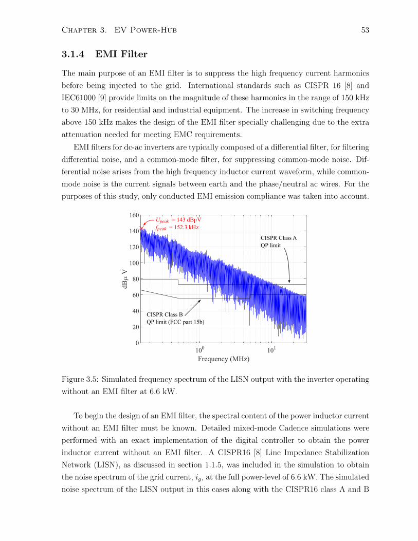
Chapter 3. EV Power-Hub 53
3.1.4 EMI Filter
The main purpose of an EMI filter is to suppress the high frequency current harmonics
before being injected to the grid. International standards such as CISPR 16 [8] and
IEC61000 [9] provide limits on the magnitude of these harmonics in the range of 150 kHz
to 30 MHz, for residential and industrial equipment. The increase in switching frequency
above 150 kHz makes the design of the EMI filter specially challenging due to the extra
attenuation needed for meeting EMC requirements.
EMI filters for dc-ac inverters are typically composed of a differential filter, for filtering
differential noise, and a common-mode filter, for suppressing common-mode noise. Dif-
ferential noise arises from the high frequency inductor current waveform, while common-
mode noise is the current signals between earth and the phase/neutral ac wires. For the
purposes of this study, only conducted EMI emission compliance was taken into account.
100 101
Frequency (MHz)
0
20
40
60
80
100
120
140
160
dBV
CISPR Class AQP limit
CISPR Class BQP limit (FCC part 15b)
Upeak = 143 dB Vfpeak = 152.3 kHz
Figure 3.5: Simulated frequency spectrum of the LISN output with the inverter operating
without an EMI filter at 6.6 kW.
To begin the design of an EMI filter, the spectral content of the power inductor current
without an EMI filter must be known. Detailed mixed-mode Cadence simulations were
performed with an exact implementation of the digital controller to obtain the power
inductor current without an EMI filter. A CISPR16 [8] Line Impedance Stabilization
Network (LISN), as discussed in section 1.1.5, was included in the simulation to obtain
the noise spectrum of the grid current, ig, at the full power-level of 6.6 kW. The simulated
noise spectrum of the LISN output in this cases along with the CISPR16 class A and B
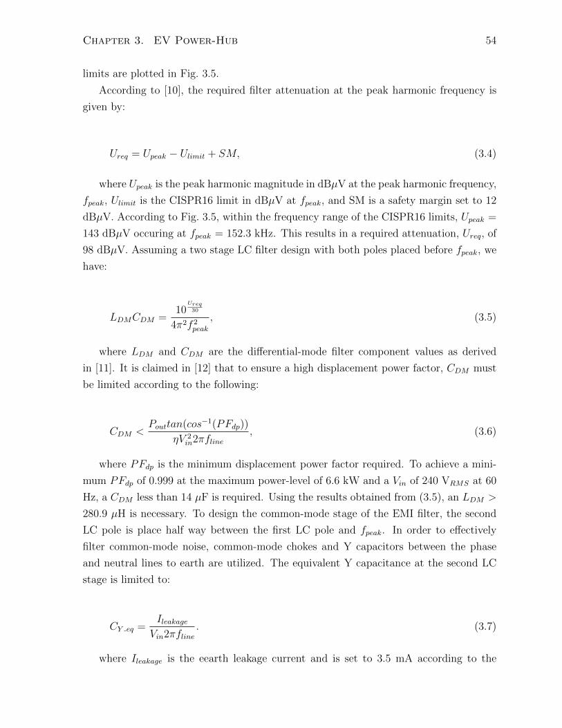
Chapter 3. EV Power-Hub 54
limits are plotted in Fig. 3.5.
According to [10], the required filter attenuation at the peak harmonic frequency is
given by:
Ureq = Upeak − Ulimit + SM, (3.4)
where Upeak is the peak harmonic magnitude in dBµV at the peak harmonic frequency,
fpeak, Ulimit is the CISPR16 limit in dBµV at fpeak, and SM is a safety margin set to 12
dBµV. According to Fig. 3.5, within the frequency range of the CISPR16 limits, Upeak =
143 dBµV occuring at fpeak = 152.3 kHz. This results in a required attenuation, Ureq, of
98 dBµV. Assuming a two stage LC filter design with both poles placed before fpeak, we
have:
LDMCDM =10
Ureq30
4π2f 2peak
, (3.5)
where LDM and CDM are the differential-mode filter component values as derived
in [11]. It is claimed in [12] that to ensure a high displacement power factor, CDM must
be limited according to the following:
CDM <Pouttan(cos−1(PFdp))
ηV 2in2πfline
, (3.6)
where PFdp is the minimum displacement power factor required. To achieve a mini-
mum PFdp of 0.999 at the maximum power-level of 6.6 kW and a Vin of 240 VRMS at 60
Hz, a CDM less than 14 µF is required. Using the results obtained from (3.5), an LDM >
280.9 µH is necessary. To design the common-mode stage of the EMI filter, the second
LC pole is place half way between the first LC pole and fpeak. In order to effectively
filter common-mode noise, common-mode chokes and Y capacitors between the phase
and neutral lines to earth are utilized. The equivalent Y capacitance at the second LC
stage is limited to:
CY eq =IleakageVin2πfline
. (3.7)
where Ileakage is the eearth leakage current and is set to 3.5 mA according to the

Chapter 3. EV Power-Hub 55
CISPR 22 standard specifications [13]. This results in CY eq = 38.7 nF and LCM = 1.4
mH. Using the component values calculated, the final designed EMI filter is shown in
Fig. 3.6.
Vac
+
-
Differential-mode filter Common-mode filter
LDM/2 = 140 H
LDM/2 = 140 H
CDM = 14 F 33 nF25 nF
25 nF
10 nF
LCM = 1.5 mHCY equivalent
Figure 3.6: Circuit diagram of the implemented power-hub EMI filter with the associated
component values.
101 102 103 104 105 106 107 108-300
-200
-100
0
Mag
nitu
de (d
B)
101 102 103 104 105 106 107 108
Frequency (Hz)
-360
-180
0
Phas
e (D
egre
es)
-74.8 dB
Figure 3.7: Simulated input to output current transfer function magnitude and phase of
the power-hub EMI filter.

Chapter 3. EV Power-Hub 56
To test the performance of the designed EMI filter, another set of Cadence simulation
was run with the EMI filter in the circuit. As a conducted EMI pre-compliance measure,
the CISPR22 spectrum limits are overlayed on Figs. 3.8 and clearly shows that the
designed EMI filter is attenuating the current harmonics by 78 dB, in comparison to the
original spectrum shown in Fig. 3.5. The simultions were carried out with a maximum
step size of 5ns and the FFT of the LISN output was taken with a bin width of 1 kHz.
The CISPR 16 standard specifies a bin width of 9 kHz for analyzing the spectral content
of the signal, meaning that the simulated spectrum is slightly exaggerated. Taking peak
values for the FFT calculation, further exaggerates the spectrum results as the CISPR 16
standard also specifies the use of a quasi-peak detector. The simulated transfer function
of the implemented EMI filter from input to output current is shown in Fig. 3.7.
100 101
Frequency (MHz)
0
20
40
60
80
100
120
140
160
dBV
CISPR Class AQP limit
CISPR Class BQP limit (FCC part 15b)
Figure 3.8: Simulated frequency spectrum of the LISN output with the inverter operating
with an EMI filter at 6.6 kW.
3.1.5 Controller and Isolation
The controller was implemented on a Xilinx Spartan 3E FPGA with digital isolators
transferring the DAC data bus and the HCMC comparator signals. The two DACs
shared the same 12 bit data bus interleaved with two separate clocks. A differential
amplifier with a unity-gain bandwidth of 200 MHz was selected for the current sensing.
The components used for the inverter controller are presented in table. 3.3.

Chapter 3. EV Power-Hub 57
Table 3.3: Specifications for the Power-Hub Controller Components
Specification Value
FPGA XC3S500e-4VQ100, 50 MHz clocked [14]
Current sensor AD8129, 200 MHz, differential amplifier [15]
DAC AD9742, 12 bits, 210 MSPS [16]
Comparator TLV3502, 4.5 ns comparator [17]
Digital isolator SI8645, 10 ns, quad-channel digital isolator [18]
3.1.6 Auxiliary Power Supply
The auxiliary power supply is an isolated, four output, current mode controlled flyback
converter with a nominal power rating of 4 Watts and an input of 12 V from the EV
auxiliary low voltage battery. The generated outputs are 12 V for the gate drive voltage
and ±5 V for the HCMC control circuitry. Another isolated 5 V is also generated for the
FPGA and isolator supply voltages. Dedicated Low Dropout Regulators (LDOs), which
are situated on the main power-stage PCB, are utilized to step down the HCMC ±5 V
voltages to ±3.3 V. The ADuM3190 [19] isolated error amplifier was used for voltage
feedback. The power-hub also contains an off-the-shelf 12 W ac-dc adapter which derives
an additional 12 V auxiliary supply from the input ac line. This secondary 12 V supply
is diode OR’ed with the LV auxiliary battery of the EV to prevent unwanted blackout
conditions.
+5 V
-5 V
+12 V
+5 V (FPGA)Vin = +12 V
Figure 3.9: Auxiliary power supply for the power-hub.

Chapter 3. EV Power-Hub 58
3.1.7 Thermal Design
At the peak operating condition of 6.6 kW, the thermal management system must dis-
sipate 416 W from the MOSFETs and 176.1 W from the power inductors, from both
the inverter and the DAB converter stages combined. The core section of the cooling
system is a liquid-cooled aluminum plate with embedded copper tubes that uses a water
and glycol mixture as the coolant. This aluminum plate, as shown in Fig. 3.10, acts
as the heat sink for the MOSFETs and also as the bottom structure of the waterproof
enclosure of the power-hub. Developing an integrated cooling solution for the MOS-
FETs and power inductors is particularly challenging in this design because of the high
switching frequency operation of the converter, which induces high eddy current loses
when electrically conductive elements are placed in direct contact or in close proximity
of the magnetic components. The heat from the low-side MOSFETs, which are placed
on the bottom side of the PCB, is rejected to the heat sink through pure conduction, by
installing the PCB directly on top of the aluminum plate, while the high-side MOSFETs
which are placed on the top side of the PCB are thermally coupled to the aluminum plate
via integrated heat-pipes. Electrically insulated thermal pads are used as the interface
material between the PCB and the aluminum chill plate.
Coolant in
Coolant out
Magnetic Components
EMI filter
DC bus capacitorsFans
Aluminumchill plate
Heat-pipes
Heat exchanger
Inverter
Figure 3.10: Mechanical and thermal design of the power-hub. The magnetic components
are cooled with air flow, and the MOSFETs are cooled with the liquid cooled aluminum
chill plate.

Chapter 3. EV Power-Hub 59
For cooling the power inductors, two potential thermal solutions were considered:
1. recirculation of air within the enclosure of the power-hub while exchanging heat
with the bottom chill plate through an assembly of aluminum fins and heat pipes
as in [20],
2. submerging the magnetics in thermal potting epoxy enclosed in a metal case that
exchanges heat to the heat sink through pure conduction or through an assembly
of heat-pipes as done in [21].
The second option has the benefit of acting as a shock absorber for the inductors
and increases the mechanical integrity of the magnetic components [22]. However, this
method is not selected due to the necessity of a vacuum chamber for proper potting and
creating a uniform bubble-free contact with the inductors is a challenging task [23]. To
implement the first option, rows of aluminum fins need to be placed at the center of the
power-hub PCB, with a dedicated fan blowing air through the heat-exchanger. A bundle
of heat pipes connect the heat exchanger on the top side of the PCB to the bottom
aluminum plate ensuring low thermal resistance to the base heat sink. It must be noted
that this thermal design is not implemented at the time of this writing, and preliminary
thermal simulations have been used to validate the described cooling approach.
3.2 Experimental Results
This section goes over the operation of the EV power-hub in the V2H, V2G, G2V, and the
V2V modes. The behaviour of the HCMC controller and power sharing among paralleled
MOSFETs is also presented. Finally, analysis is presented on the results of the detailed
Cadence simulations as well as the experimental efficiency and THD measurements. It
must be noted that all the presented experimental results were obtained without the
thermal system implemented, as a result, the thermal performance of the system is not
measured.
3.2.1 HCMC Operation
The ideal inductor waveforms shown in Fig. 2.2 and Fig. 2.3 are realized with a pair
of 12-bit DACs that shape the inductor peak and valley current envelopes. The DAC
outputs that shape Ipk and Ivly over the ac line cycle are shown in Fig. 3.11(b) for hybrid-
mode operation. The inductor current iL and the sensed IR signal, Vsense, along with
corresponding comparator trigger points, are shown in Fig. 3.11(a). To avoid switching

Chapter 3. EV Power-Hub 60
frequencies above 400 kHz at the zero crossings, a zero-average current region is imposed,
and ∆I is maintained to 2 A. The presence of the zero-average current region introduces
nonlinearities and undesirable THD to Iavg.
iL
Ipk
Ivly
Vsense
comp_high asserted
comp_low asserted
5 s/div
(a)
BCM CCM
1/120 s
2ms/divIpk
Ivly
(b)
Figure 3.11: HCMC operation with the (a) iL and IR waveforms and instances when the
comparator output signals are asserted in BCM operation. (b) Peak and valley envelopes
for the inductor current for a line cycle in hybrid-mode operation.
3.2.2 Parallel SiC MOSFET Operation
Equal power and current sharing among paralleled switching devices is necessary to pre-
vent over-stressing and over-heating MOSFETs. There are two main forms of power
sharing among paralleled MOSFETs: static and dynamic. Static power sharing is re-
ferred to equal power dissipation during the on-time of the devices only, whilst dynamic
power sharing considers the power dissipation mismatch during the turn-on and turn-off
intervals. In paralleled MOSFET switch-mode power converters, static power sharing
imbalance is inherently overcome due to the positive temperature coefficient of MOS-
FET drain-to-source Ron [24]. Dynamic power sharing is normally caused due to the
mismatch of package bond wire inductance, MOSFET threshhold voltage mismatch, and
PCB parasitics [25]. To reduce the effects of dynamic power sharing mismatch in the
EV power-hub, each paralleled MOSFET has a dedicated gate resistor which is slightly
modified iteratively to ensure balanced operation. The precise matching of gate-to-source
voltages, vgs, of a pair of paralleled MOSFETs with 5 A drain current during the turn-on
and turn-off instances are shown in Figs. 3.12(a) and (b), respectively.

Chapter 3. EV Power-Hub 61
iL
vgs1vgs2
(a)
iL
vgs1
vgs2
(b)
Figure 3.12: Gate to source voltage of a pair of paralleled high-side MOSFETs switching
5 A.
The usage of SMD devices for the power-stage prevents the direct measurement of
drain current to verify equal dynamic power sharing. As a result, the thermal performance
of each MOSFET is taken as a measure for balanced operation. Very similar MOSFET
temperatures among paired MOSFETs, as shown in Fig. 3.13, verifies a closely matched
power sharing at a power-level of 1 kW. Since the thermal system is not implemented,
steady state thermal operation cannot be reached and measured, hence, as a comparative
measure, the operation of the converter was timed equally in every run to provide a fair
comparison.
(a) (b)
Figure 3.13: (a) power sharing among the first high-side pair MOSFETs, (b) power
sharing among each low-side pair MOSFETs at a power-level of 1 kW.

Chapter 3. EV Power-Hub 62
3.2.3 V2H Operation
The V2H operating mode was tested using a single-phase resistive load at 240 VRMS.
The operation of the inverter in BCM at 2.3 kW and in hybrid mode at 5 kW are shown
in Figs. 3.14(a) and (b), respectively.
iL
vac
iac
(a)
iLiac
vac
(b)
Figure 3.14: Experimental operation of the power-hub in the V2H mode operating in
(a)BCM at a power-level of 2.3 kW, and (b) in hybrid mode at a power-level of 5 kW.
All waveforms are taken with 450 VDC input and an output of 240 Vrms.
3.2.4 V2G/G2V Operation
The V2G and G2V operating modes are tested by connecting the ac port of the power-
hub to the 208 V single-phase grid via a 60 Hz isolation transformer. The output of the
grid phase locking comparator is inverted to switch between the V2G and G2V operating
modes. The V2G operation of the inverter in BCM at 2.5 kW and in hybrid mode at 3
kW are shown in Figs. 3.15(a) and (b), respectively.
iLiac
vac
(a)
iL iac
vac
(b)
Figure 3.15: Experimental operation of the power-hub in the V2G mode operating in
(a)BCM at a power-level of 2.5 kW, and (b) in hybrid mode at a power-level of 3 kW.
Both waveforms are taken with 450 VDC input and an output of 208 Vrms.
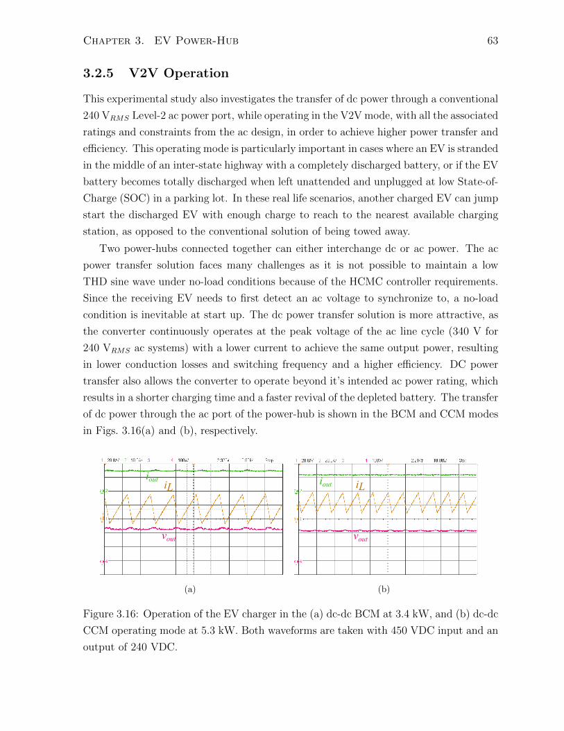
Chapter 3. EV Power-Hub 63
3.2.5 V2V Operation
This experimental study also investigates the transfer of dc power through a conventional
240 VRMS Level-2 ac power port, while operating in the V2V mode, with all the associated
ratings and constraints from the ac design, in order to achieve higher power transfer and
efficiency. This operating mode is particularly important in cases where an EV is stranded
in the middle of an inter-state highway with a completely discharged battery, or if the EV
battery becomes totally discharged when left unattended and unplugged at low State-of-
Charge (SOC) in a parking lot. In these real life scenarios, another charged EV can jump
start the discharged EV with enough charge to reach to the nearest available charging
station, as opposed to the conventional solution of being towed away.
Two power-hubs connected together can either interchange dc or ac power. The ac
power transfer solution faces many challenges as it is not possible to maintain a low
THD sine wave under no-load conditions because of the HCMC controller requirements.
Since the receiving EV needs to first detect an ac voltage to synchronize to, a no-load
condition is inevitable at start up. The dc power transfer solution is more attractive, as
the converter continuously operates at the peak voltage of the ac line cycle (340 V for
240 VRMS ac systems) with a lower current to achieve the same output power, resulting
in lower conduction losses and switching frequency and a higher efficiency. DC power
transfer also allows the converter to operate beyond it’s intended ac power rating, which
results in a shorter charging time and a faster revival of the depleted battery. The transfer
of dc power through the ac port of the power-hub is shown in the BCM and CCM modes
in Figs. 3.16(a) and (b), respectively.
iL
vout
iout
(a)
iLiout
vout
(b)
Figure 3.16: Operation of the EV charger in the (a) dc-dc BCM at 3.4 kW, and (b) dc-dc
CCM operating mode at 5.3 kW. Both waveforms are taken with 450 VDC input and an
output of 240 VDC.

Chapter 3. EV Power-Hub 64
iR
Rsense
Vin
+
-
Cin
DigitalCurrent
Modulator
D/A
D/A
Control
Logic
Current Loop
A/D
vsense
FilterEMI
DTControl
DTControl
25 H
PICurrent scaling
Mode selection: V2V
Vbus_ref iR
Rsense
V
+
-
C
DigitalCurrent
Modulator
D/A
D/A
Control
Logic
Current Loop
A/D
vsense
FilterEMI
DTControl
DTControl
25 H
Current scaling
Mode selection: V2V
ConstantVmin
Enable
iL1(t) iL3(t)
L3
L4+
-Vlink
ilink
outout
+-
Power-hub A Power-hub B
Figure 3.17: Two power-hubs, which are designed and optimized for ac power transfer,
are setup in the V2V mode to transfer dc power.
To test the V2V mode in a more realistic scenario, the output ports of power-hub A
and B are connected as shown in Fig. 3.17, and the link voltage, Vlink, is regulated by
power-hub A to a set reference, Vbus ref , as part of an outer voltage-loop. Each EMI
filter, which is optimized for the ac charging operation, includes 10 µF of capacitance
that is necessary for the HCMC controller operation and eliminates the need for an
external dc link capacitor. As soon as power-hub B detects a voltage at the dc link, the
battery charging process begins with a flipped current direction through L3 by reversing
the MOSFET switching sequence. The auxiliary supply voltages for each power-hub
are derived from a secondary LV battery and a self-regulating universal dc-ac adapter
connected to the output port of the converter. These two independent voltage sources
are diode-ORed to prevent any black-out condition especially for power-hub B, which
might also have a depleted LV auxiliary battery. The experimental results of the V2V
operating mode at 1 kW power-level is shown in Fig. 3.18
iL3
iL1
Vlink
ilink
Figure 3.18: Measured waveforms demonstrating the operation of two power-hubs in the
V2V operating mode.

Chapter 3. EV Power-Hub 65
3.2.6 Efficiency and Loss Analysis
Detailed mixed-mode Cadence simulations were performed with the C3M0065090J MOS-
FET spice model and an exact implementation of the digital controller to characterize
the loss distribution of the power-hub in each of the four modes of operation, i.e. dc-ac
BCM, dc-ac hybrid, dc-dc BCM, and dc-dc CCM. The simulation includes HDL models
for the controller and Verilog-a models for data converters. For every operating mode,
Cadence simulations were carried out to obtain the total MOSFET losses (conduction
and switching combined), sensing losses, and EMI filter losses. The switching losses were
obtained according to:
Pswitching = PMOSFET sim − 2IRMS2Ron, (3.8)
where PMOSFET sim is the total simulated MOSFET loss and IRMS is the simulated
inductor RMS current. The total experimental loss of the converter was then measured
by running the system in each operating mode at the simulation power-level. Then, the
magnetic losses are derived using:
Pmagnetics = Ptotal loss exp−(Ploss MOSFET sim+Ploss sensing sim+Ploss emi filter sim), (3.9)
where Ptotal loss exp is the total experimental loss, Ploss MOSFET sim is the total simu-
lated MOSFET loss, Ploss sensing sim is the total simulated sensing loss, and Ploss emi filter sim
is the simulated EMI filter loss. Core losses are isolated from Pmagnetics by:
Pcore = Pmagnetics − 2IRMS2Rwinding ac, (3.10)
where IRMS is the simulated inductor RMS current and Rwinding ac is the measured
ac winding resistance of each inductor at the average switching frequency of 100 kHz.
Since low frequency 60 Hz currents flow through the EMI filter, the EMI filter magnetic
losses are negligible and therefore ignored from the calculations.
In the dc-ac BCM case, inductor core losses is the most significant source of loss
and MOSFET switching losses comprise of only 22% of the total power dissipation, as
evident in Fig. 3.19(a). This is because of the large inductor current ripple and ZVS
turn-on of the MOSFETs. In the dc-ac hybrid mode, switching losses are significantly
increased due to the loss of soft-switching at the line cycle peaks and troughs, as shown
in Fig. 3.19(b). The inductor core losses are, however, decreased due to lower current
ripple. The dc-dc BCM operating mode is least dissipative due to soft-switching and
having the lowest switching frequency. In the dc-dc CCM case the losses are still lower
than the dc-ac hybrid mode even though the power-level is 2 kW higher, as presented in
Chapter 3. EV Power-Hub 66
Figs. 3.19(d) and (b).
MOSFETconduction (6%)
MOSFETswitching (22%)
Inductorcore (63%)
Inductorwinding (7%)
Sensing (2%)EMI filter (1%)
DC-AC BCM @ 2.3 kW 100% = 115.03 W
(a)
DC-AC Hybrid @ 5 kW 100% = 188.87 W
Inductorcore (29%)
MOSFETswitching (30%)
MOSFETconduction (18%) Inductor
winding (19%)
Sensing (2%)EMI filter (2%)
(b)
DC-DC BCM @ 3.4 kW 100% = 79.91 W
MOSFETconduction (22%)
MOSFETswitching (26%) Inductor
core (19%)
Inductorwinding (24%)
Sensing (4%)EMI filter (5%)
(c)
DC-DC CCM @ 5.3 kW 100% = 174.01 W
MOSFETswitching (16%)
MOSFETconduction (28%)
Inductorcore (17%)
Inductorwinding (30%)
Sensing (3%)EMI filter (6%)
(d)
Figure 3.19: Simulated loss breakdown of the power-hub in the (a) dc-ac BCM (2.3 kW),
(b) dc-ac BCM/CCM hybrid (5 kW), (c) dc-dc BCM (3.4 kW), and (d) dc-dc CCM
operating mode (5.3 kW). Vin=450 VDC, Vout=340 VDC.
In the dc-dc operating mode, as opposed to the dc-ac mode, a constant dc output
voltage results in higher achievable power-levels. For the same average inductor current,
the power-level increases proportional to the output dc voltage, as shown in Fig. 3.20(a).
In the BCM only mode, there is an increase in efficiency going from dc-ac to dc-dc
operation and with higher output dc voltages due to lower switching frequencies and
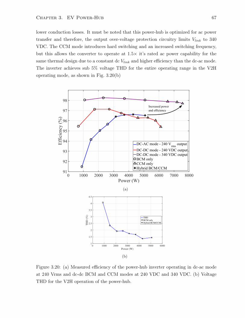
Chapter 3. EV Power-Hub 67
lower conduction losses. It must be noted that this power-hub is optimized for ac power
transfer and therefore, the output over-voltage protection circuitry limits Vlink to 340
VDC. The CCM mode introduces hard switching and an increased switching frequency,
but this allows the converter to operate at 1.5× it’s rated ac power capability for the
same thermal design due to a constant dc Vlink and higher efficiency than the dc-ac mode.
The inverter achieves sub 5% voltage THD for the entire operating range in the V2H
operating mode, as shown in Fig. 3.20(b)
0 1000 2000 3000 4000 5000 6000 7000 8000Power (W)
91
92
93
94
95
96
97
98
Effic
ienc
y (%
)
DC-AC mode - 240 Vrms outputDC-DC mode - 240 VDC outputDC-DC mode - 340 VDC outputBCM onlyCCM onlyHybrid BCM/CCM
Increased powerand efficiency
(a)
0 1000 2000 3000 4000 5000 6000
Power (W)
1
1.5
2
2.5
3
3.5
4
4.5
TH
D (
%)
THD
BCM only
Hybrid BCM/CCM
(b)
Figure 3.20: (a) Measured efficiency of the power-hub inverter operating in dc-ac mode
at 240 Vrms and dc-dc BCM and CCM modes at 240 VDC and 340 VDC. (b) Voltage
THD for the V2H operation of the power-hub.
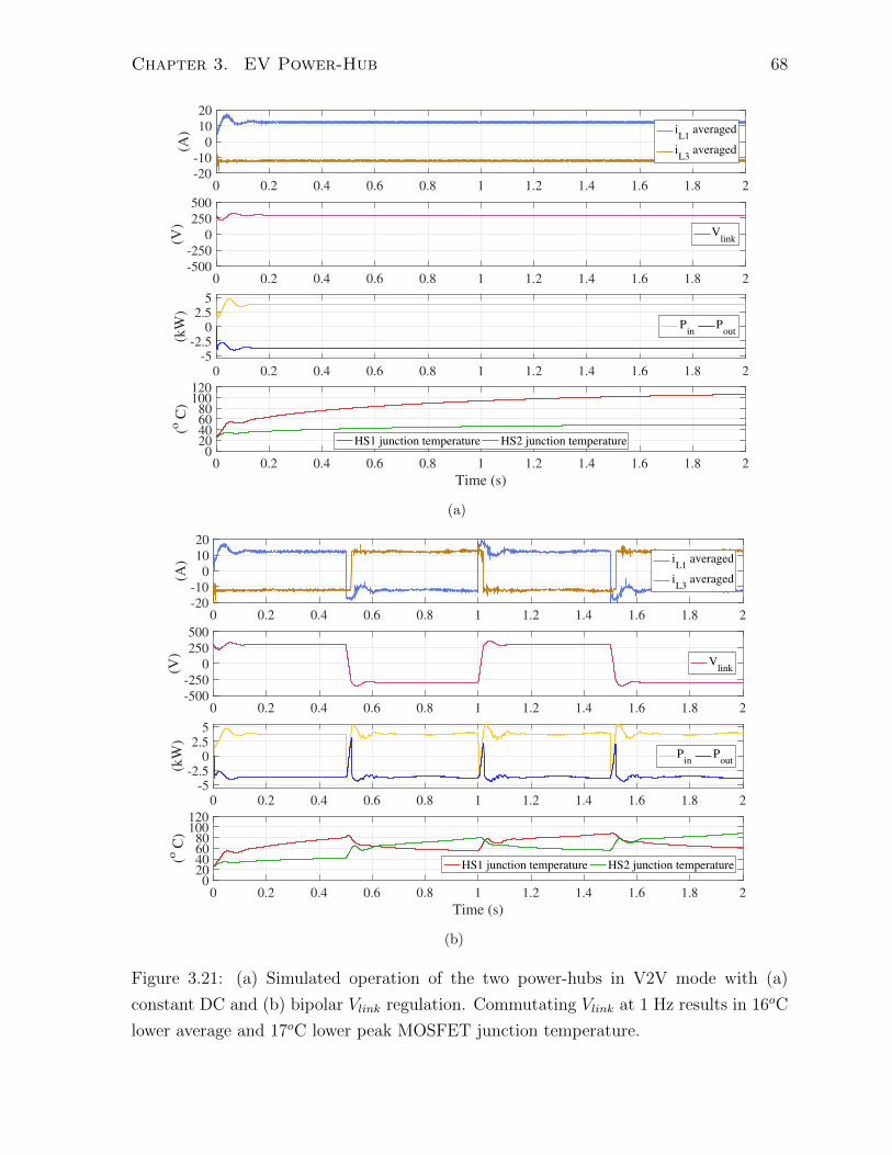
Chapter 3. EV Power-Hub 68
0 0.2 0.4 0.6 0.8 1 1.2 1.4 1.6 1.8 2-20
-10
0
10
20
(A) i
L1 averaged
iL3
averaged
0 0.2 0.4 0.6 0.8 1 1.2 1.4 1.6 1.8 2-500
-250
0
250
500
(V)
Vlink
0 0.2 0.4 0.6 0.8 1 1.2 1.4 1.6 1.8 2-5
-2.50
2.55
(kW
)
Pin
Pout
0 0.2 0.4 0.6 0.8 1 1.2 1.4 1.6 1.8 2
Time (s)
020406080
100120
(o C
)
HS1 junction temperature HS2 junction temperature
(a)
0 0.2 0.4 0.6 0.8 1 1.2 1.4 1.6 1.8 2-20
-10
0
10
20
(A) i
L1 averaged
iL3
averaged
0 0.2 0.4 0.6 0.8 1 1.2 1.4 1.6 1.8 2-500
-250
0
250
500
(V)
Vlink
0 0.2 0.4 0.6 0.8 1 1.2 1.4 1.6 1.8 2-5
-2.50
2.55
(kW
)
Pin
Pout
0 0.2 0.4 0.6 0.8 1 1.2 1.4 1.6 1.8 2
Time (s)
020406080
100120
(o C
)
HS1 junction temperature HS2 junction temperature
(b)
Figure 3.21: (a) Simulated operation of the two power-hubs in V2V mode with (a)
constant DC and (b) bipolar Vlink regulation. Commutating Vlink at 1 Hz results in 16oC
lower average and 17oC lower peak MOSFET junction temperature.
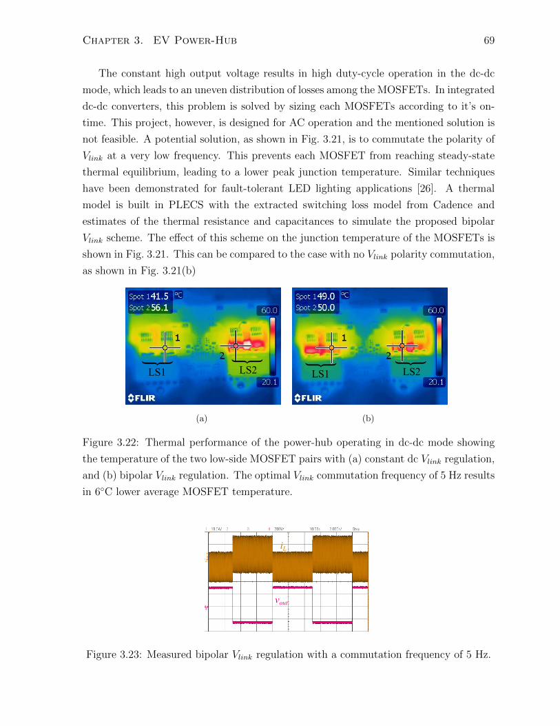
Chapter 3. EV Power-Hub 69
The constant high output voltage results in high duty-cycle operation in the dc-dc
mode, which leads to an uneven distribution of losses among the MOSFETs. In integrated
dc-dc converters, this problem is solved by sizing each MOSFETs according to it’s on-
time. This project, however, is designed for AC operation and the mentioned solution is
not feasible. A potential solution, as shown in Fig. 3.21, is to commutate the polarity of
Vlink at a very low frequency. This prevents each MOSFET from reaching steady-state
thermal equilibrium, leading to a lower peak junction temperature. Similar techniques
have been demonstrated for fault-tolerant LED lighting applications [26]. A thermal
model is built in PLECS with the extracted switching loss model from Cadence and
estimates of the thermal resistance and capacitances to simulate the proposed bipolar
Vlink scheme. The effect of this scheme on the junction temperature of the MOSFETs is
shown in Fig. 3.21. This can be compared to the case with no Vlink polarity commutation,
as shown in Fig. 3.21(b)
LS1 LS2
(a)
LS1 LS2
(b)
Figure 3.22: Thermal performance of the power-hub operating in dc-dc mode showing
the temperature of the two low-side MOSFET pairs with (a) constant dc Vlink regulation,
and (b) bipolar Vlink regulation. The optimal Vlink commutation frequency of 5 Hz results
in 6C lower average MOSFET temperature.
iL
vout
Figure 3.23: Measured bipolar Vlink regulation with a commutation frequency of 5 Hz.
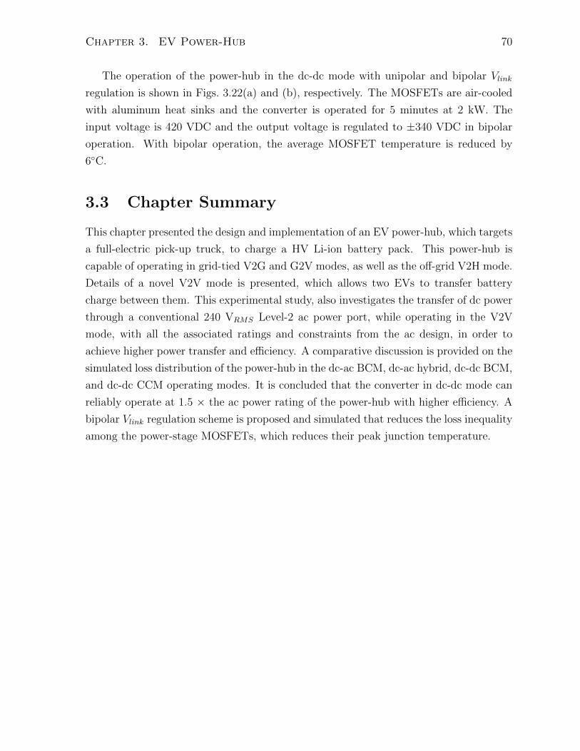
Chapter 3. EV Power-Hub 70
The operation of the power-hub in the dc-dc mode with unipolar and bipolar Vlink
regulation is shown in Figs. 3.22(a) and (b), respectively. The MOSFETs are air-cooled
with aluminum heat sinks and the converter is operated for 5 minutes at 2 kW. The
input voltage is 420 VDC and the output voltage is regulated to ±340 VDC in bipolar
operation. With bipolar operation, the average MOSFET temperature is reduced by
6C.
3.3 Chapter Summary
This chapter presented the design and implementation of an EV power-hub, which targets
a full-electric pick-up truck, to charge a HV Li-ion battery pack. This power-hub is
capable of operating in grid-tied V2G and G2V modes, as well as the off-grid V2H mode.
Details of a novel V2V mode is presented, which allows two EVs to transfer battery
charge between them. This experimental study, also investigates the transfer of dc power
through a conventional 240 VRMS Level-2 ac power port, while operating in the V2V
mode, with all the associated ratings and constraints from the ac design, in order to
achieve higher power transfer and efficiency. A comparative discussion is provided on the
simulated loss distribution of the power-hub in the dc-ac BCM, dc-ac hybrid, dc-dc BCM,
and dc-dc CCM operating modes. It is concluded that the converter in dc-dc mode can
reliably operate at 1.5 × the ac power rating of the power-hub with higher efficiency. A
bipolar Vlink regulation scheme is proposed and simulated that reduces the loss inequality
among the power-stage MOSFETs, which reduces their peak junction temperature.
References
[1] M. Nasr, K. M. Gupta, C. D. Silva, and O. Trescases, “Sic based on-board ev
power-hub with high-efficiency dc transfer mode through ac port for vehicle-to-
vehicle charging,” in 2018 IEEE Applied Power Electronics Conference and Ex-
position (APEC), March 2018.
[2] “Cree 900v sic mosfet,” CREE-Wolfspeed Datasheet, available
http://www.wolfspeed.com/media/downloads/145/C3M0065090J.pdf.
[3] “Texas instruments 5.6 kv, 6 a, isolated gate driver,” Texas Instruments Datasheet,
available http://www.ti.com/lit/ds/sluscj9b/sluscj9b.pdf.
[4] Y. Tang and F. Blaabjerg, “Power decoupling techniques for single-phase power
electronics systems; an overview,” in 2015 IEEE Energy Conversion Congress and
Exposition (ECCE), Sept 2015, pp. 2541–2548.
[5] P. T. Krein, R. S. Balog, and M. Mirjafari, “Minimum energy and capacitance
requirements for single-phase inverters and rectifiers using a ripple port,” IEEE
Transactions on Power Electronics, vol. 27, no. 11, pp. 4690–4698, Nov 2012.
[6] L. H. Dixon, “Magnetics design for switching power sup-
plies [application note],” Texas Instruments Inc., 2001, available
https://www.ti.com/lit/ml/slup127/slup127.pdf.
[7] W. G. Hurley and Z. Ouyang, “High frequency planar magnetics for
power conversion [apec 2017 education seminar],” National University
of Ireland and Technical University of Denmark (DTU), 2017, available
http://orbit.dtu.dk/files/131741663/APEC 2017 Presentation.pdf.
[8] “Specification for radio disturbance and immunity measuring apparatus and meth-
ods - Part 1-2: Radio disturbance and immunity measuring apparatus - Coupling
devices for conducted disturbance measurements,” Canadian Standards Association,
Ontario, Canada, Standard, Mar. 2014.
71

REFERENCES 72
[9] “Electromagnetic compatibility (EMC) - Part 3-2: Limits - Limits for harmonic
current emissions (equipment input current; 16 A per phase),” International Elec-
trotechnical Commission, Geneva, CH, Standard, May 2014.
[10] K. Raggl, T. Nussbaumer, and J. W. Kolar, “Guideline for a simplified differential-
mode emi filter design,” IEEE Transactions on Industrial Electronics, vol. 57, no. 3,
pp. 1031–1040, March 2010.
[11] G. Ala, G. C. Giaconia, G. Giglia, M. C. D. Piazza, M. Luna, G. Vitale, and
P. Zanchetta, “Optimized design of high power density emi filters for power electronic
converters,” in 2016 AEIT International Annual Conference (AEIT), Oct 2016, pp.
1–6.
[12] H. Choi, “Design consideration for interleaved boundary conduction mode
pfc using fan9611/12 [application note],” ON Semiconductor, 2009, available
https://www.fairchildsemi.com/application-notes/AN/AN-6086.pdf.
[13] C. Buob, “Functionality of line filters - leakage currents in the right
perspective [white paper],” Farnell - Element 14, 2007, available
http://www.farnell.com/datasheets/1712865.pdf.
[14] “Xilinx spartan-3e fpga family data sheet product specification,” Xilinx Datasheet,
available https://www.xilinx.com/support/documentation/data sheets/ds312.pdf.
[15] “Low cost 270 mhz differential receiver amplifiers ad8129/ad8130,” Analog
Devices Inc. Datasheet, available http://www.analog.com/media/en/technical-
documentation/data-sheets/AD8129 8130.pdf.
[16] “12-bit, 210 msps txdac digital-to-analog converter,” Analog Devices Inc. Datasheet,
available http://www.analog.com/media/en/technical-documentation/data-
sheets/AD9742.pdf.
[17] “Tlv350x 4.5-ns, rail-to-rail, high-speed comparator in microsize packages,” Texas
Instruments Datasheet, available http://www.ti.com/lit/ds/symlink/tlv3502.pdf.
[18] “Low-power quad-channel digital isolators,” Silicon Labs Datasheet, available
https://www.silabs.com/documents/public/data-sheets/si864x-datasheet.pdf.
[19] “High stability isolated error amplifier,” Analog Devices Inc. Datasheet,
available http://www.analog.com/media/en/technical-documentation/data-
sheets/ADuM3190.pdf.
REFERENCES 73
[20] T. B. Gradinger and U. Drofenik, “Analysis and comparison of air and water cooled
inductors for medium-voltage power-electronic applications,” in 8th IET Interna-
tional Conference on Power Electronics, Machines and Drives (PEMD 2016), April
2016, pp. 1–6.
[21] D. Hewitt, D. Stone, and M. Foster, “Modelling the enhancement to the thermal
performance of encapsulants using thermally conductive filler materials,” in PCIM
Asia 2015; International Exhibition and Conference for Power Electronics, Intelli-
gent Motion, Renewable Energy and Energy Management, June 2015, pp. 1–8.
[22] J. F. Maddox, R. W. Knight, and S. H. Bhavnani, “Non-uniform thermal properties
of an alumina granule/epoxy potting compound,” in 2010 12th IEEE Intersociety
Conference on Thermal and Thermomechanical Phenomena in Electronic Systems,
June 2010, pp. 1–6.
[23] B. G. You, B. K. Lee, S.-W. Lee, M.-C. Jeong, J.-H. Kim, and I.-B. Jeong, “Improve-
ment of the thermal flow with potting structured inductor for high power density
in 40kw dc-dc converter,” in 2012 IEEE Vehicle Power and Propulsion Conference,
Oct 2012, pp. 1027–1032.
[24] G. Wang, J. Mookken, J. Rice, and M. Schupbach, “Dynamic and static behavior of
packaged silicon carbide mosfets in paralleled applications,” in 2014 IEEE Applied
Power Electronics Conference and Exposition - APEC 2014, March 2014, pp. 1478–
1483.
[25] Y. Mao, Z. Miao, K. D. T. Ngo, and C. M. Wang, “Balancing of peak currents
between paralleled sic mosfets by source impedances,” in 2017 IEEE Applied Power
Electronics Conference and Exposition (APEC), March 2017, pp. 800–803.
[26] S. Zhao, K. Cao, S. Firwana, A. Swaris, R. Content, and O. Trescases, “Failsafe
smart led module with thermal management, string current balancing and com-
mutation for lifetime extension,” in 2012 IEEE Energy Conversion Congress and
Exposition (ECCE), Sept 2012, pp. 4246–4253.
Chapter 4
Modular, Off-grid PV Inverter
This chapter presents the implementation details and experimental results of a modular
off-grid inverter targeted for PV applications. As discussed in section 1.3.3, the total 2
kW single-phase AC power rating of the inverter is handled by three paralleled single-
phase sub-inverters each rated at 667 W. The implementation section covers details on
the sub-inverter, inductor, EMI filter, APD capacitor, auxiliary power supply, and the
thermal/mechanical design. The experimental results section goes over the efficiency
and THD performance, transient behaviour, APD testings, and light load efficiency im-
provements. The chapter concludes with a comparative analysis on similar PV inverter
prototypes.
4.1 Modular, Off-Grid PV Inverter Implementation
The PV inverter has many differences in comparison to the EV power-hub, mainly due
to the lower power-level, lower volume requirements, and modified cooling constraints.
The lower power-level indicates that not only the power-stage needs to be re-optimized,
but also modified and more optimal inductors must be made by taking size and ther-
mal performance into consideration. Lower volume requirements results in a completely
different PCB and mechanical design. Not only is the overall architecture modular, con-
sisting of dedicated sub-inverters, but each sub-inverter is implemented modularly with
the power-stage and controller on two separate PCBs. The following section goes over
the implementation details of the off-grid inverter including power-stage, controller, in-
ductors, EMI filter, APD capacitor bank, auxiliary power supply, and the interface PCB.
In this work the electrical and mechanical systems were iteratively co-designed using
detailed 3D thermal and air-flow simulations.
74
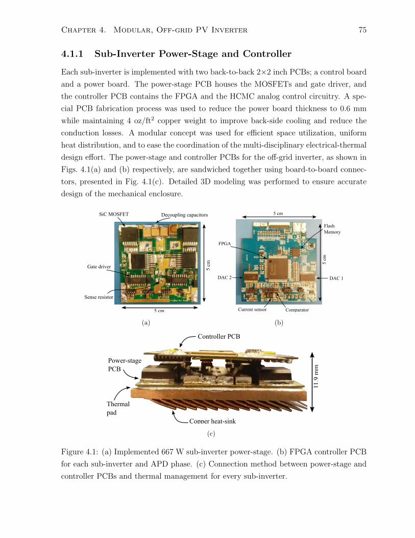
Chapter 4. Modular, Off-grid PV Inverter 75
4.1.1 Sub-Inverter Power-Stage and Controller
Each sub-inverter is implemented with two back-to-back 2×2 inch PCBs; a control board
and a power board. The power-stage PCB houses the MOSFETs and gate driver, and
the controller PCB contains the FPGA and the HCMC analog control circuitry. A spe-
cial PCB fabrication process was used to reduce the power board thickness to 0.6 mm
while maintaining 4 oz/ft2 copper weight to improve back-side cooling and reduce the
conduction losses. A modular concept was used for efficient space utilization, uniform
heat distribution, and to ease the coordination of the multi-disciplinary electrical-thermal
design effort. The power-stage and controller PCBs for the off-grid inverter, as shown in
Figs. 4.1(a) and (b) respectively, are sandwiched together using board-to-board connec-
tors, presented in Fig. 4.1(c). Detailed 3D modeling was performed to ensure accurate
design of the mechanical enclosure.
SiC MOSFET
Gate driver
Sense resistor
Decoupling capacitors5
cm
5 cm
(a)
DAC 1DAC 2
FPGA
Current sensor Comparator
FlashMemory
5 cm
5 cm
(b)
Controller PCB
Power-stage PCB
Copper heat-sink
Thermal pad
11.9
mm
(c)
Figure 4.1: (a) Implemented 667 W sub-inverter power-stage. (b) FPGA controller PCB
for each sub-inverter and APD phase. (c) Connection method between power-stage and
controller PCBs and thermal management for every sub-inverter.
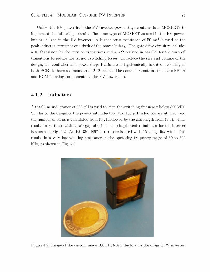
Chapter 4. Modular, Off-grid PV Inverter 76
Unlike the EV power-hub, the PV inverter power-stage contains four MOSFETs to
implement the full-bridge circuit. The same type of MOSFET as used in the EV power-
hub is utilized in the PV inverter. A higher sense resistance of 50 mΩ is used as the
peak inductor current is one sixth of the power-hub iL. The gate drive circuitry includes
a 10 Ω resistor for the turn on transitions and a 5 Ω resistor in parallel for the turn off
transitions to reduce the turn-off switching losses. To reduce the size and volume of the
design, the controller and power-stage PCBs are not galvanically isolated, resulting in
both PCBs to have a dimension of 2×2 inches. The controller contains the same FPGA
and HCMC analog components as the EV power-hub.
4.1.2 Inductors
A total line inductance of 200 µH is used to keep the switching frequency below 300 kHz.
Similar to the design of the power-hub inductors, two 100 µH inductors are utilized, and
the number of turns is calculated from (3.2) followed by the gap length from (3.3), which
results in 30 turns with an air gap of 0.1cm. The implemented inductor for the inverter
is shown in Fig. 4.2. An EFD30, N97 ferrite core is used with 15 gauge litz wire. This
results in a very low winding resistance in the operating frequency range of 30 to 300
kHz, as shown in Fig. 4.3
Figure 4.2: Image of the custom made 100 µH, 6 A inductors for the off-grid PV inverter.

Chapter 4. Modular, Off-grid PV Inverter 77
103 104 105 106 107
Frequency (Hz)
0
500
1000
1500
2000
Win
ding
resi
stan
ce (m
)124.03m @ 30kHz
262.6m @ 300kHz
1.49 @ 1MHz
fs
Figure 4.3: Measured winding AC resistance of the PV inverter inductors versus fre-
quency.
4.1.3 EMI Filter
An approach similar to the power-hub EMI filter design is taken by incorporating a two-
stage LC network comprising of a front-stage differential filter followed by a common-
mode LC filter. The simulated spectrum of the LISN output in the absence of an EMI
filter is shown in Fig. 4.6(a). A maximum harmonics peak of 145.1 dBµV is measured at
fpeak = 330.5 kHz. Using (3.4), 97.6 dBµV of filter attenuation is required to suppress the
peak harmonic to under the CISPR class B limit. From (3.5) and (3.6), LDM and CDM
are calculated to be 68 µH and 4.6 µF respectively. This results in a resonant frequency
of 7 kHz, for the differential filter stage. The common-mode filter pole is placed half way
between fpeak and the first filter pole, resulting in a pole frequency of 100 kHz. To meet
the leakage current requirements, CCM and LCM are calculated to be 38 nF and 635 µH,
respectively.
Vac
+
-
Differential-mode filter Common-mode filter
CY equivalentLDM/2 = 45 H
LDM/2 = 45 H
CDM = 4 F 30 nF25 nF
25 nF
LCM = 635 H
33 nF
Figure 4.4: Circuit diagram of the implemented PV inverter EMI filter with the associated
component values.

Chapter 4. Modular, Off-grid PV Inverter 78
The simulated frequency response of the implemented EMI filter showing the neces-
sary filter attenuation of 97 dBµV is provided in Fig. 4.5.
101 102 103 104 105 106 107 108-300
-200
-100
0
Mag
nitu
de (d
B)
101 102 103 104 105 106 107 108
Frequency (Hz)
-360
-180
0
Phas
e (D
egre
es)
-96.5 dB
Figure 4.5: Simulated input to output current transfer function magnitude and phase of
the PV inverter EMI filter.
100 101
Frequency (MHz)
0
20
40
60
80
100
120
140
160
dBV
CISPR Class AQP limit
CISPR Class BQP limit (FCC part 15b)
Upeak = 145 dB Vfpeak = 330 kHz
(a)
100 101
Frequency (MHz)
0
20
40
60
80
100
120
140
160
dBV
CISPR Class AQP limit
CISPR Class BQP limit (FCC part 15b)
(b)
Figure 4.6: Simulated peak frequency spectrum of the LISN output (a) in the absence
of an EMI filter, and (b) with the designed EMI filter included. Both simulations were
carried out at 2 kW output power and the FFT bin width is set to 1 kHz.
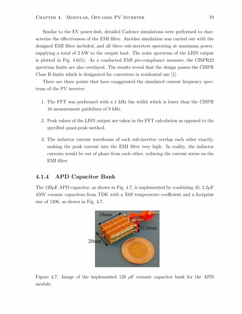
Chapter 4. Modular, Off-grid PV Inverter 79
Similar to the EV power-hub, detailed Cadence simulations were performed to char-
acterize the effectiveness of the EMI filter. Another simulation was carried out with the
designed EMI filter included, and all three sub-inverters operating at maximum power,
supplying a total of 2 kW to the output load. The noise spectrum of the LISN output
is plotted in Fig. 4.6(b). As a conducted EMI pre-compliance measure, the CISPR22
spectrum limits are also overlayed. The results reveal that the design passes the CISPR
Class B limits which is designated for converters in residential use [1].
There are three points that have exaggerated the simulated current frequency spec-
trum of the PV inverter:
1. The FFT was performed with a 1 kHz bin width which is lower than the CISPR
16 measurement guidelines of 9 kHz.
2. Peak values of the LISN output are taken in the FFT calculation as opposed to the
specified quasi-peak method.
3. The inductor current waveforms of each sub-inverter overlap each other exactly,
making the peak current into the EMI filter very high. In reality, the inductor
currents would be out of phase from each other, reducing the current stress on the
EMI filter.
4.1.4 APD Capacitor Bank
The 120µF APD capacitor, as shown in Fig. 4.7, is implemented by combining 45, 2.2µF
450V ceramic capacitors from TDK with a X6S temperature coefficient and a footprint
size of 1206, as shown in Fig. 4.7.
28mm
20mm
11.5mm
Figure 4.7: Image of the implemented 120 µF ceramic capacitor bank for the APD
module.
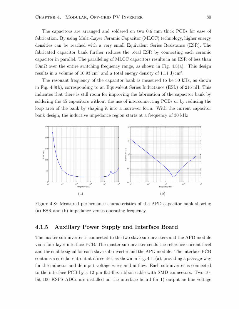
Chapter 4. Modular, Off-grid PV Inverter 80
The capacitors are arranged and soldered on two 0.6 mm thick PCBs for ease of
fabrication. By using Multi-Layer Ceramic Capacitor (MLCC) technology, higher energy
densities can be reached with a very small Equivalent Series Resistance (ESR). The
fabricated capacitor bank further reduces the total ESR by connecting each ceramic
capacitor in parallel. The paralleling of MLCC capacitors results in an ESR of less than
50mΩ over the entire switching frequency range, as shown in Fig. 4.8(a). This design
results in a volume of 10.93 cm3 and a total energy density of 1.11 J/cm3.
The resonant frequency of the capacitor bank is measured to be 30 kHz, as shown
in Fig. 4.8(b), corresponding to an Equivalent Series Inductance (ESL) of 216 nH. This
indicates that there is still room for improving the fabrication of the capacitor bank by
soldering the 45 capacitors without the use of interconnecting PCBs or by reducing the
loop area of the bank by shaping it into a narrower form. With the current capacitor
bank design, the inductive impedance region starts at a frequency of 30 kHz
101
102
103
104
105
106
Frequency (Hz)
0
50
100
150
200
250
ES
R (
m)
(a)
102
103
104
105
106
Frequency (Hz)
10-2
10-1
100
101
102
Imp
edan
ce (
)
(b)
Figure 4.8: Measured performance characteristics of the APD capacitor bank showing
(a) ESR and (b) impedance versus operating frequency.
4.1.5 Auxiliary Power Supply and Interface Board
The master sub-inverter is connected to the two slave sub-inverters and the APD module
via a four layer interface PCB. The master sub-inverter sends the reference current level
and the enable signal for each slave sub-inverter and the APD module. The interface PCB
contains a circular cut-out at it’s center, as shown in Fig. 4.11(a), providing a passage-way
for the inductor and dc input voltage wires and airflow. Each sub-inverter is connected
to the interface PCB by a 12 pin flat-flex ribbon cable with SMD connectors. Two 10-
bit 100 KSPS ADCs are installed on the interface board for 1) output ac line voltage
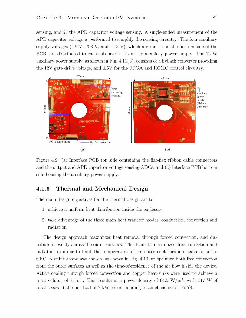
Chapter 4. Modular, Off-grid PV Inverter 81
sensing, and 2) the APD capacitor voltage sensing. A single-ended measurement of the
APD capacitor voltage is performed to simplify the sensing circuitry. The four auxiliary
supply voltages (+5 V, -3.3 V, and +12 V), which are routed on the bottom side of the
PCB, are distributed to each sub-inverter from the auxiliary power supply. The 12 W
auxiliary power supply, as shown in Fig. 4.11(b), consists of a flyback converter providing
the 12V gate drive voltage, and ±5V for the FPGA and HCMC control circuitry.
67 m
m
67 mm
APDcap votlagesensing
AC voltage sensing Flat-flex connectors
(a)
67 m
m
67 mm
Auxiliary PowerSupply(FlybackConverter)
(b)
Figure 4.9: (a) Interface PCB top side containing the flat-flex ribbon cable connectors
and the output and APD capacitor voltage sensing ADCs, and (b) interface PCB bottom
side housing the auxiliary power supply.
4.1.6 Thermal and Mechanical Design
The main design objectives for the thermal design are to
1. achieve a uniform heat distribution inside the enclosure,
2. take advantage of the three main heat transfer modes, conduction, convection and
radiation.
The design approach maximizes heat removal through forced convection, and dis-
tribute it evenly across the outer surfaces. This leads to maximized free convection and
radiation in order to limit the temperature of the outer enclosure and exhaust air to
60C. A cubic shape was chosen, as shown in Fig. 4.10, to optimize both free convection
from the outer surfaces as well as the time-of-residence of the air flow inside the device.
Active cooling through forced convection and copper heat-sinks were used to achieve a
total volume of 31 in3. This results in a power-density of 64.5 W/in3, with 117 W of
total losses at the full load of 2 kW, corresponding to an efficiency of 95.5%.
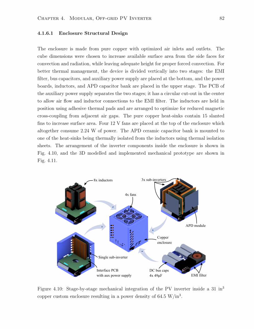
Chapter 4. Modular, Off-grid PV Inverter 82
4.1.6.1 Enclosure Structural Design
The enclosure is made from pure copper with optimized air inlets and outlets. The
cube dimensions were chosen to increase available surface area from the side faces for
convection and radiation, while leaving adequate height for proper forced convection. For
better thermal management, the device is divided vertically into two stages: the EMI
filter, bus capacitors, and auxiliary power supply are placed at the bottom, and the power
boards, inductors, and APD capacitor bank are placed in the upper stage. The PCB of
the auxiliary power supply separates the two stages; it has a circular cut-out in the center
to allow air flow and inductor connections to the EMI filter. The inductors are held in
position using adhesive thermal pads and are arranged to optimize for reduced magnetic
cross-coupling from adjacent air gaps. The pure copper heat-sinks contain 15 slanted
fins to increase surface area. Four 12 V fans are placed at the top of the enclosure which
altogether consume 2.24 W of power. The APD ceramic capacitor bank is mounted to
one of the heat-sinks being thermally isolated from the inductors using thermal isolation
sheets. The arrangement of the inverter components inside the enclosure is shown in
Fig. 4.10, and the 3D modelled and implemented mechanical prototype are shown in
Fig. 4.11.
EMI filterDC bus caps4x 49 F
Interface PCBwith aux power supply
Single sub-inverter
8x inductors 3x sub-inverters
APD module
4x fans
Copper enclosure
Figure 4.10: Stage-by-stage mechanical integration of the PV inverter inside a 31 in3
copper custom enclosure resulting in a power density of 64.5 W/in3.

Chapter 4. Modular, Off-grid PV Inverter 83
(a)
8 cm8 cm 8 cm(b)
Figure 4.11: (a) 3D modelled image of the PV inverter, and (b) the final implemented
mechanical prototype of the inverter.
4.1.6.2 Enclosure-level Cooling
InductorsSub-inverter
(a)
Inductors
Sub-inverter
(b)
Figure 4.12: (a) Vertical and (b) horizontal cross-sectional views of the inverter depicting
the airflow direction and passages for inductor and power-stage cooling.
The enclosure is designed to have two sets of air inlets: bottom inlet and side inlets.
The bottom inlet allows air to directly enter the center of the enclosure and cool the
inductors and the power-stage heat-sinks, as shown in Fig. 4.12(a). The side inlets allow
air to pass across the power-stage PCBs and assist in the cooling of the MOSFETs, as
depicted in Fig. 4.12(b). The air entering the enclosure from the sides rotates around
the power-stage PCBs in the rotational direction of the fans. As this air flow heats up it
Chapter 4. Modular, Off-grid PV Inverter 84
becomes less dense and rises towards the top of the enclosure due to gravity. This results
in a spiral flow of air upwards and the four fans on the top of the enclosure blow air out
of the system making maximum use of this gravity effect.
4.1.6.3 Power-board and Passive Component Cooling
All power boards are mounted vertically to the sides of the enclosure and attached to
low profile, pure copper heat-sinks with slanted fins that increase their surface area.
The eight power inductors are attached to the sides of the heat-sink using a thermally
conductive heat spreader with a thickness of 1mm. This thickness is very important
as the high frequency inductor current can cause eddy current losses within electrically
conductive material in close proximity. Power MOSFETs are cooled from the bottom side
via the PCB to the heat-sink and from the upper side via a thermally conductive heat
spreader. Extensive thermal simulations of the full system is done in ANSYS, including
all major power-dissipating electronic components, a faithful representation of internal
components and air flow paths, and the air flow curves of the fans. Thermal simulations
show that with a maximum distributed power loss of 117 W, the surface temperature of
the enclosure would be less than 40C, a maximum air temperature of 55.2C at the air
outlet, and an air velocity of 4.65 m/s.
4.2 Experimental Results
This section presents the simulation and experimental results of the PV inverter. The
trade-offs between BCM and hybrid modes of operation is also analysed. Results on the
APD phase, sub-inverter-shedding, and transient performance is also demonstrated.
4.2.1 Single Sub-Inverter Operation
The implementation of the entire modular off-grid PV inverter begins by verifying the
operation of a single sub-inverter and characterizing the performance of the controller and
the power-stage. To reduce the chances of trial-and-error mistakes in the controller design
phase, detailed mixed-mode Cadence simulations were performed with the C3M0065090J
MOSFET spice model and an exact implementation of the digital controller to charac-
terize the loss distribution of the PV inverter. The simulation includes HDL models for
the controller and Verilog-a models for data converters. These simulations also help in
analysing converter losses and thermal performance. After the HDL controller has been

Chapter 4. Modular, Off-grid PV Inverter 85
designed in simulation, the sub-inverter is experimentally verified outside of the designed
enclosure to characterize it’s thermal performance.
4.2.1.1 Mixed-Mode Cadence Simulation
The Cadence simulation testbench for a single sub-inverter consists of an HDL controller,
power-stage, an EMI filter module as discussed in section 4.1.3, and the ac resistive load,
as shown in Fig. 4.13. The 450 V input voltage source is modeled with a 10 Ω series
resistor as specified by the requirements. The simulation results for two ac line cycles in
the BCM and hybrid mode is shown in Figs. 4.14(a) and (b), respectively. The line cycle
frequency was accelerated to 240 Hz to reduce the simulation run time.
HCMC Controller
Power-stage EMI filter
iL
Vac
Figure 4.13: Cadence simulation testbench for a single sub-inverter.
0 2 4 6 8
Time (s) 10-3
-6
-3
0
3
6
Am
ps
(A) i
L
0 2 4 6 8
Time (s) 10-3
-400
-200
0
200
400
Vo
lts
(V) V
ac
(a)
0 2 4 6 8
Time (s) 10-3
-6
-3
0
3
6
Am
ps
(A) i
L
0 2 4 6 8
Time (s) 10-3
-400
-200
0
200
400
Vo
lts
(V) V
ac
(b)
Figure 4.14: Simulation results for the off-grid PV inverter operating in (a) BCM at a
power-level of 254.5 W, and (b) hybrid mode at a power-level of 594 W. Both simulations
were carried out with a 450 VDC input voltage and 240 Vrms.
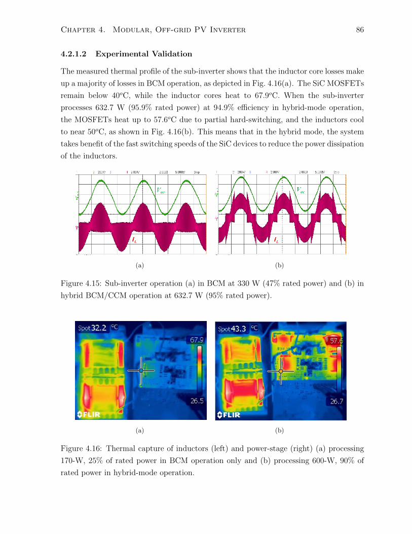
Chapter 4. Modular, Off-grid PV Inverter 86
4.2.1.2 Experimental Validation
The measured thermal profile of the sub-inverter shows that the inductor core losses make
up a majority of losses in BCM operation, as depicted in Fig. 4.16(a). The SiC MOSFETs
remain below 40oC, while the inductor cores heat to 67.9oC. When the sub-inverter
processes 632.7 W (95.9% rated power) at 94.9% efficiency in hybrid-mode operation,
the MOSFETs heat up to 57.6oC due to partial hard-switching, and the inductors cool
to near 50oC, as shown in Fig. 4.16(b). This means that in the hybrid mode, the system
takes benefit of the fast switching speeds of the SiC devices to reduce the power dissipation
of the inductors.
(a) (b)
Figure 4.15: Sub-inverter operation (a) in BCM at 330 W (47% rated power) and (b) in
hybrid BCM/CCM operation at 632.7 W (95% rated power).
(a) (b)
Figure 4.16: Thermal capture of inductors (left) and power-stage (right) (a) processing
170-W, 25% of rated power in BCM operation only and (b) processing 600-W, 90% of
rated power in hybrid-mode operation.
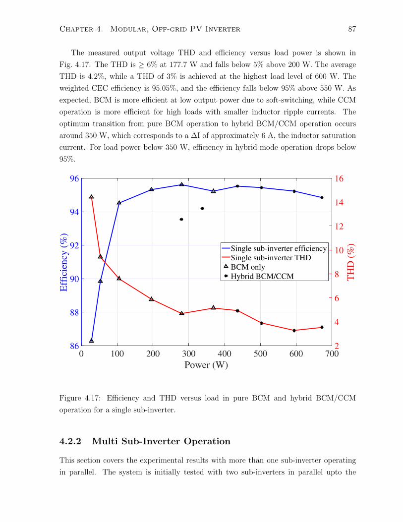
Chapter 4. Modular, Off-grid PV Inverter 87
The measured output voltage THD and efficiency versus load power is shown in
Fig. 4.17. The THD is ≥ 6% at 177.7 W and falls below 5% above 200 W. The average
THD is 4.2%, while a THD of 3% is achieved at the highest load level of 600 W. The
weighted CEC efficiency is 95.05%, and the efficiency falls below 95% above 550 W. As
expected, BCM is more efficient at low output power due to soft-switching, while CCM
operation is more efficient for high loads with smaller inductor ripple currents. The
optimum transition from pure BCM operation to hybrid BCM/CCM operation occurs
around 350 W, which corresponds to a ∆I of approximately 6 A, the inductor saturation
current. For load power below 350 W, efficiency in hybrid-mode operation drops below
95%.
0 100 200 300 400 500 600 700
Power (W)
86
88
90
92
94
96
Eff
icie
ncy
(%
)
2
4
6
8
10
12
14
16
TH
D (
%)
Single sub-inverter efficiency
Single sub-inverter THD
BCM only
Hybrid BCM/CCM
Figure 4.17: Efficiency and THD versus load in pure BCM and hybrid BCM/CCM
operation for a single sub-inverter.
4.2.2 Multi Sub-Inverter Operation
This section covers the experimental results with more than one sub-inverter operating
in parallel. The system is initially tested with two sub-inverters in parallel upto the

Chapter 4. Modular, Off-grid PV Inverter 88
full power rating of each sub-inverter. Finally, all three sub-inverters are connected and
operation was verified up to the maximum 2 kW power-level.
4.2.2.1 Mixed-Mode Cadence Simulation
Cadence simulations were also run with all three sub-inverters operating at 2 kW output
power. The simulation testbench, as shown in Fig. 4.18, contains a master sub-inverter
which sends the 60 Hz synchronization signal and the RMS current reference, iref , to the
other two slave sub-inverters. The slave sub-inverter controller module generates the Ipk
and Ivly HCMC signals in sync with the master and scaled according to iref . Identical
to the architectural drawing in Fig. 1.12, each sub-inverter has two 100 µH inductors
which are connected to a common node entering the EMI filter. The 240 Hz line cycle
frequency simulation results are shown in Fig. 4.19.
Vac
iL1
iL2
iL3
EMI filter
Sub-inverter 1 (master)
Sub-inverter 2 (slave)
Sub-inverter 3 (slave)
Figure 4.18: Mixed-mode Cadence simulation testbench for parallel sub-inverter opera-
tion.
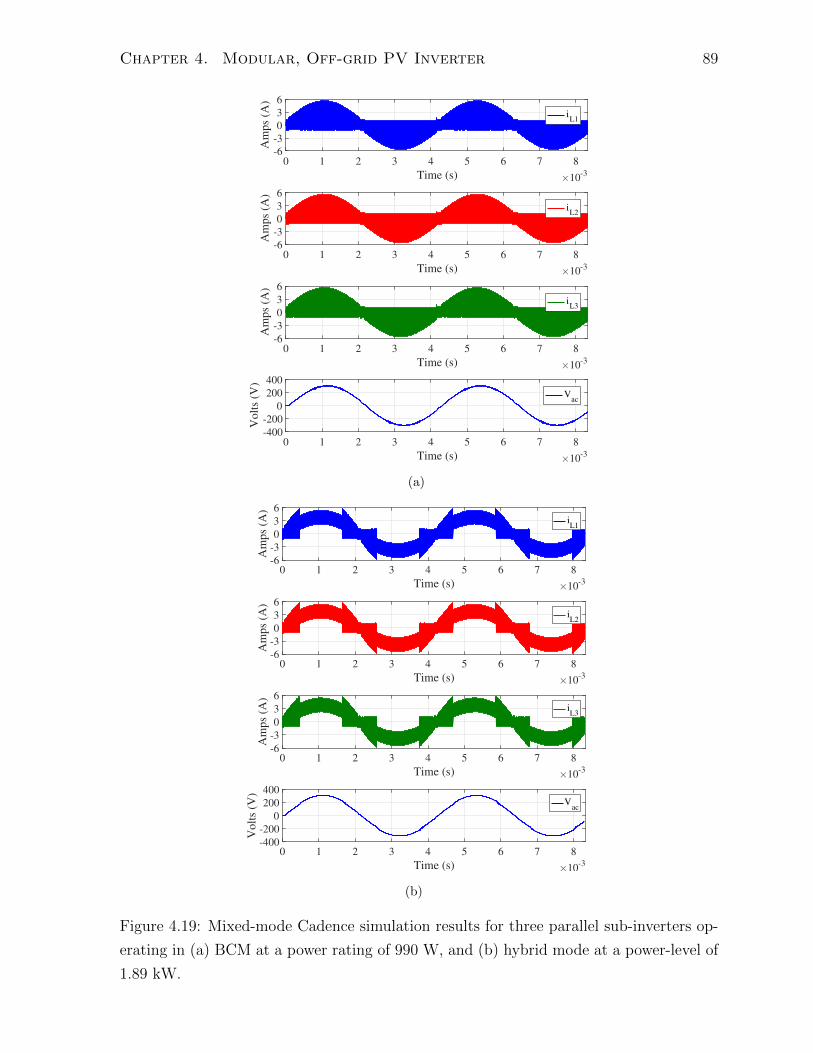
Chapter 4. Modular, Off-grid PV Inverter 89
0 1 2 3 4 5 6 7 8
Time (s) 10-3
-6
-3
0
3
6
Am
ps
(A)
iL1
0 1 2 3 4 5 6 7 8
Time (s) 10-3
-6
-3
0
3
6
Am
ps
(A)
iL2
0 1 2 3 4 5 6 7 8
Time (s) 10-3
-6
-3
0
3
6
Am
ps
(A)
iL3
0 1 2 3 4 5 6 7 8
Time (s) 10-3
-400
-200
0
200
400
Vo
lts
(V)
Vac
(a)
0 1 2 3 4 5 6 7 8
Time (s) 10-3
-6
-3
0
3
6
Am
ps
(A)
iL1
0 1 2 3 4 5 6 7 8
Time (s) 10-3
-6
-3
0
3
6
Am
ps
(A)
iL2
0 1 2 3 4 5 6 7 8
Time (s) 10-3
-6
-3
0
3
6
Am
ps
(A)
iL3
0 1 2 3 4 5 6 7 8
Time (s) 10-3
-400
-200
0
200
400
Vo
lts
(V)
Vac
(b)
Figure 4.19: Mixed-mode Cadence simulation results for three parallel sub-inverters op-
erating in (a) BCM at a power rating of 990 W, and (b) hybrid mode at a power-level of
1.89 kW.
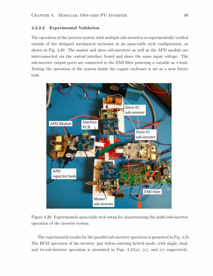
Chapter 4. Modular, Off-grid PV Inverter 90
4.2.2.2 Experimental Validation
The operation of the inverter system with multiple sub-inverters is experimentally verified
outside of the designed mechanical enclosure in an open-table style configuration, as
shown in Fig. 4.20. The master and slave sub-inverters as well as the APD module are
interconnected via the central interface board and share the same input voltage. The
sub-inverter output ports are connected to the EMI filter powering a variable ac e-load.
Testing the operation of the system inside the copper enclosure is set as a near future
task.
Master sub-inverter
Slave #1 sub-inverter
Slave #2 sub-inverter
APD Module
APDcapacitor bank
EMI filter
InterfacePCB
Figure 4.20: Experimental open-table style setup for characterizing the multi-sub-inverter
operation of the inverter system.
The experimental results for the parallel sub-inverter operation is presented in Fig. 4.21.
The BCM operation of the inverter, just before entering hybrid mode, with single, dual,
and tri-sub-inverter operation is presented in Figs. 4.21(a), (c), and (e) respectively.

Chapter 4. Modular, Off-grid PV Inverter 91
Similarly, The hybrid operation of the inverter with single, dual, and tri-sub-inverter
operation is presented in Figs. 4.21(b), (d), and (f) respectively.
iL1
Vac
iL2
iL3
(a)
iL1
Vac
iL2
iL3
(b)
iL1
iL2Vac
iL3
(c)
iL1
iL2Vac
iL3
(d)
iL1
iL2
iL3
Vac
(e)
iL1
iL2
iL3
Vac
(f)
Figure 4.21: Experimental waveforms of the inverter operation with (a) single sub-
inverter BCM operation at 368 W, and (b) hybrid operation at 660 W. (c) Dual sub-
inverter BCM operation at 736 W, and (d) hybrid operation at 1.32 kW. (e) Tri sub-
inverter BCM operation at 1.1 kW, and (f) hybrid operation at 1.93 kW. All waveforms
were captured with 450 VDC input and 240 Vrms output voltage.
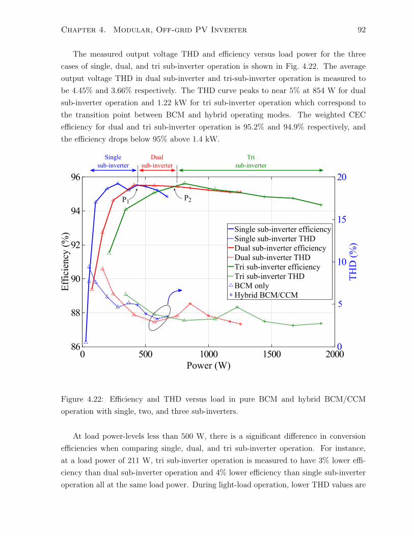
Chapter 4. Modular, Off-grid PV Inverter 92
The measured output voltage THD and efficiency versus load power for the three
cases of single, dual, and tri sub-inverter operation is shown in Fig. 4.22. The average
output voltage THD in dual sub-inverter and tri-sub-inverter operation is measured to
be 4.45% and 3.66% respectively. The THD curve peaks to near 5% at 854 W for dual
sub-inverter operation and 1.22 kW for tri sub-inverter operation which correspond to
the transition point between BCM and hybrid operating modes. The weighted CEC
efficiency for dual and tri sub-inverter operation is 95.2% and 94.9% respectively, and
the efficiency drops below 95% above 1.4 kW.
0 500 1000 1500 2000Power (W)
86
88
90
92
94
96
Effic
ienc
y (%
)
0
10
15
20
THD
(%)
Single sub-inverter efficiencySingle sub-inverter THDDual sub-inverter efficiencyDual sub-inverter THDTri sub-inverter efficiencyTri sub-inverter THDBCM onlyHybrid BCM/CCM
Single sub-inverter
Dual sub-inverter
Tri sub-inverter
5
P2P1
Figure 4.22: Efficiency and THD versus load in pure BCM and hybrid BCM/CCM
operation with single, two, and three sub-inverters.
At load power-levels less than 500 W, there is a significant difference in conversion
efficiencies when comparing single, dual, and tri sub-inverter operation. For instance,
at a load power of 211 W, tri sub-inverter operation is measured to have 3% lower effi-
ciency than dual sub-inverter operation and 4% lower efficiency than single sub-inverter
operation all at the same load power. During light-load operation, lower THD values are
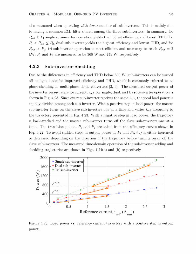
Chapter 4. Modular, Off-grid PV Inverter 93
also measured when operating with fewer number of sub-inverters. This is mainly due
to having a common EMI filter shared among the three sub-inverters. In summary, for
Pout ≤ P1 single sub-inverter operation yields the highest efficiency and lowest THD, for
P1 < Pout ≤ P2, dual sub-inverter yields the highest efficiency and lowest THD, and for
Pout > P2, tri sub-inverter operation is most efficient and necessary to reach Pout = 2
kW. P1 and P2 are measured to be 368 W and 749 W, respectively.
4.2.3 Sub-inverter-Shedding
Due to the differences in efficiency and THD below 500 W, sub-inverters can be turned
off at light loads for improved efficiency and THD, which is commonly referred to as
phase-shedding in multi-phase dc-dc converters [2, 3]. The measured output power of
the inverter versus reference current, iref , for single, dual, and tri sub-inverter operation is
shown in Fig. 4.23. Since every sub-inverter receives the same iref , the total load power is
equally divided among each sub-inverter. With a positive step in load power, the master
sub-inverter turns on the slave sub-inverters one at a time and varies iref according to
the trajectory presented in Fig. 4.23. With a negative step in load power, the trajectory
is back-tracked and the master sub-inverter turns off the slave sub-inverters one at a
time. The transition points, P1 and P2 are taken from the efficiency curves shown in
Fig. 4.22. To avoid sudden steps in output power at P1 and P2, iref is either increased
or decreased depending on the direction of the trajectory before turning on or off the
slave sub-inverters. The measured time-domain operation of the sub-inverter adding and
shedding trajectories are shown in Figs. 4.24(a) and (b) respectively.
0 0.5 1 1.5 2 2.5 3Reference current, iref, (Arms)
0
400
800
1200
1600
2000
Pow
er (W
)
Single sub-inverterDual sub-inverterTri sub-inverter
P1
P2
Figure 4.23: Load power vs. reference current trajectory with a positive step in output
power.

Chapter 4. Modular, Off-grid PV Inverter 94
iL1
iL2
iL3P2P1
(a)
iL1
iL2
iL3P2 P1
(b)
Figure 4.24: (a) Sub-inverter adding during a positive step in load power, and (b) sub-
inverter shedding during a negative step in load power.
4.2.4 Active Power Decoupling
The APD system is experimentally verified as a stand-alone module with one sub-inverter
operating. The APD module is run with 120 Hz average inductor current and an APD
capacitor voltage of 54.3 Vpk−pk at a bias voltage of 320 VDC. The effect of the APD
module is best shown by starting the APD operation while a sub-inverter is already
operating, as shown in Fig. 4.25. With a series input source resistance of 10 Ω, The APD
module reduces the bus voltage ripple by 42%. It must be noted that iLapdis enforced to
have a positive dc offset to keep the capacitor bank bias voltage at vc ref , as explained in
section 2.2.3.
Vc_apd
vbus
iL_apd
iL1
APD start
1/60 Hz
1/120 Hz
8.8 Vpk-pk 3.7 Vpk-pk
Figure 4.25: APD start-up transient with a single sub-inverter operating at 466.7 W.
The APD capacitor voltage reaches a dc offset and ripple voltage of 320 VDC and 54.3
Vpk−pk respectively. This results in a bus voltage ripple reduction of 42%.
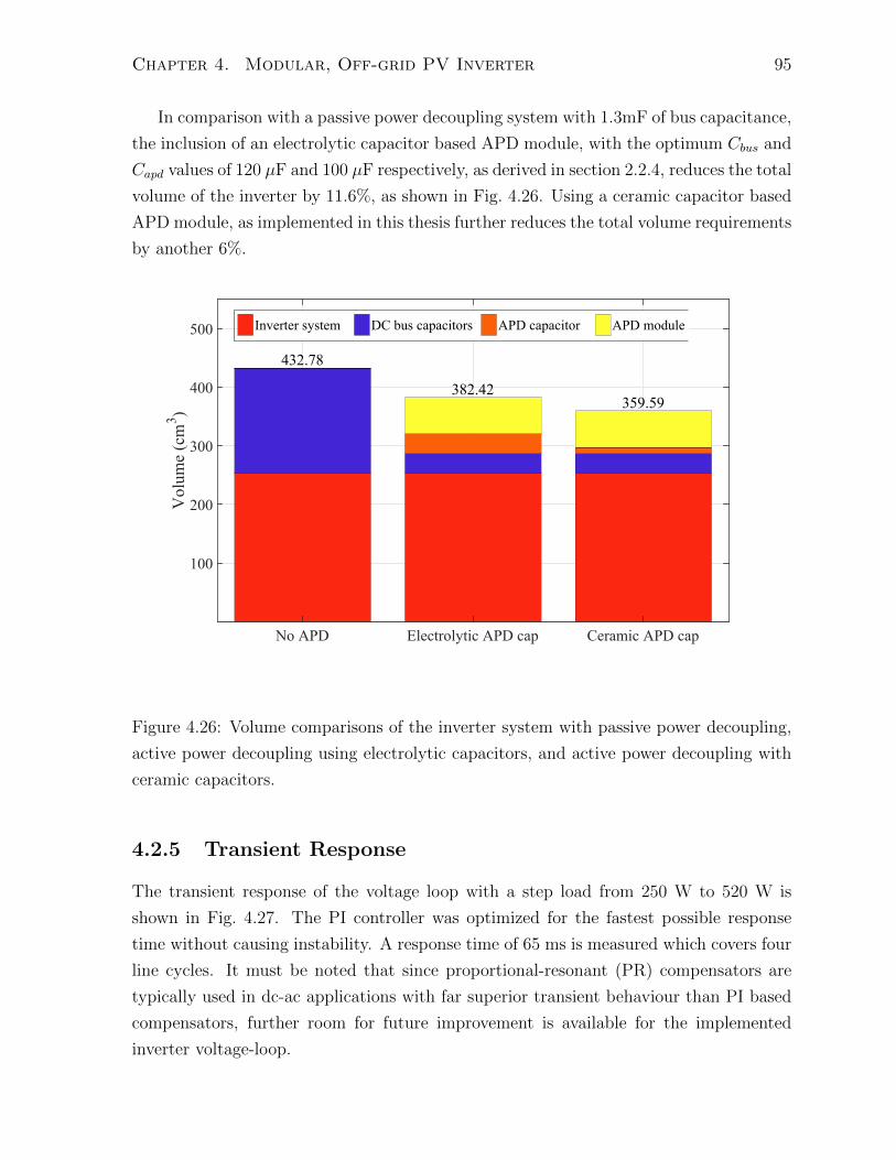
Chapter 4. Modular, Off-grid PV Inverter 95
In comparison with a passive power decoupling system with 1.3mF of bus capacitance,
the inclusion of an electrolytic capacitor based APD module, with the optimum Cbus and
Capd values of 120 µF and 100 µF respectively, as derived in section 2.2.4, reduces the total
volume of the inverter by 11.6%, as shown in Fig. 4.26. Using a ceramic capacitor based
APD module, as implemented in this thesis further reduces the total volume requirements
by another 6%.
432.78
382.42359.59
No APD Electrolytic APD cap Ceramic APD cap
100
200
300
400
500
Vol
ume
(cm
3 )
Inverter system DC bus capacitors APD capacitor APD module
Figure 4.26: Volume comparisons of the inverter system with passive power decoupling,
active power decoupling using electrolytic capacitors, and active power decoupling with
ceramic capacitors.
4.2.5 Transient Response
The transient response of the voltage loop with a step load from 250 W to 520 W is
shown in Fig. 4.27. The PI controller was optimized for the fastest possible response
time without causing instability. A response time of 65 ms is measured which covers four
line cycles. It must be noted that since proportional-resonant (PR) compensators are
typically used in dc-ac applications with far superior transient behaviour than PI based
compensators, further room for future improvement is available for the implemented
inverter voltage-loop.
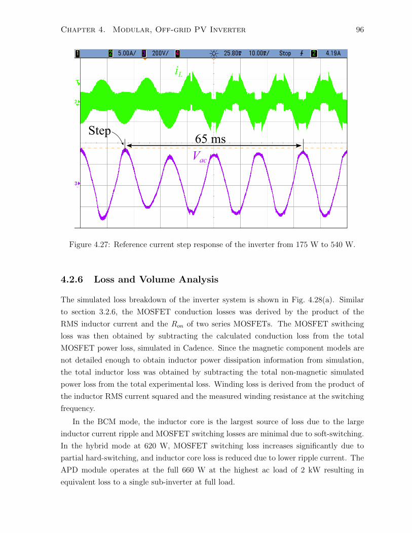
Chapter 4. Modular, Off-grid PV Inverter 96
iL
Vac
65 msStep
Figure 4.27: Reference current step response of the inverter from 175 W to 540 W.
4.2.6 Loss and Volume Analysis
The simulated loss breakdown of the inverter system is shown in Fig. 4.28(a). Similar
to section 3.2.6, the MOSFET conduction losses was derived by the product of the
RMS inductor current and the Ron of two series MOSFETs. The MOSFET swithcing
loss was then obtained by subtracting the calculated conduction loss from the total
MOSFET power loss, simulated in Cadence. Since the magnetic component models are
not detailed enough to obtain inductor power dissipation information from simulation,
the total inductor loss was obtained by subtracting the total non-magnetic simulated
power loss from the total experimental loss. Winding loss is derived from the product of
the inductor RMS current squared and the measured winding resistance at the switching
frequency.
In the BCM mode, the inductor core is the largest source of loss due to the large
inductor current ripple and MOSFET switching losses are minimal due to soft-switching.
In the hybrid mode at 620 W, MOSFET switching loss increases significantly due to
partial hard-switching, and inductor core loss is reduced due to lower ripple current. The
APD module operates at the full 660 W at the highest ac load of 2 kW resulting in
equivalent loss to a single sub-inverter at full load.

Chapter 4. Modular, Off-grid PV Inverter 97
BCM @ 375.2 W 100% = 66.05 W
Inductorcore (47%)
MOSFETswitching (22%)
MOSFETconduction (3%)
Inductorwinding (<1%)
Sensing (2%)
APD (25%)
(a)
Hybrid @ 653 W 100% = 120.13 W
Inductorcore (18%)
MOSFETswitching (52%)
MOSFETconduction (3%)
APD (25%)
Sensing (2%)Inductorwinding (<1%)
(b)
APD power-stage (8%)
APD inductors (5%)
APD cap bank (3%)
APD cooling (5%)
Power-stages (24%)
Heat sinks (14%)
Inductors (14%)
Aux supply (10%)
DC bus cap (9%)
EMI filter (7%)
Fans (2%)
Active PowerDecoupling (21%)
(c)
Figure 4.28: Simulated loss break down of the PV inverter system in (a) BCM and (b)
hybrid mode operation. (c) Volume breakdown of the PV inverter system.
The three sub-inverter power-stage and controller PCBs occupy 24% of the total
inverter volume, as shown in Fig. 4.28(c). The heat sinks and inductors both take up

Chapter 4. Modular, Off-grid PV Inverter 98
14%, and the auxiliary power supply, dc bus caps, EMI filter, and fans occupy, 10%, 9%,
7%, and 2% of the total space, respectively. The APD module accounts for 21% of the
entire volume.
4.2.7 Benchmark Comparison
The inverter designed in this chapter is compared against five commercial and five indus-
trial designs with similar power ratings and input/output voltage ranges. The commercial
comparisons are presented in table 4.1. The density achieved in this work is 7× greater
than the TSI Bravo 2.5 kW inverter which holds the lead in the commercial design list.
The PV inverter implemented in this work is also the lightest among the commercial
designs with a total mass of 1 kg.
Table 4.1: Benchmark Comparison of this Work to Five Other Commercial PV String
Inverters with Similar Power-Levels
Output Density CEC Specific
power (W) (W/in3) efficiency (%) power (W/kg)
This work 2000 64.5 95.05 2000
TSI Bravo [4] 2500 8.87 96 581.4
SBS25 [5] 2500 2.1 96.1 241.7
EnaSolar [7] 2000 1.24 94.5 142.9
Fronius 2.0-1 [6] 2000 0.578 94.9 119
ABB PVI-3.0 [8] 3000 0.531 96 93.9
In comparison to other academic single-phase PV inverters that have been finalists
in the GLB challenge, this work can not compete in terms of power density or efficiency.
It must be noted that all the academic designs presented in table 4.2, have utilized GaN
devices which is more costly but more compact.
Every commercial and academic inverter design has been plotted on an efficiency vs.
power density graph, as presented in Fig. 4.29. While the implemented PV inverter has
lower efficiency and power density than most academic designs, the usage of SiC technol-
ogy as opposed to GaN and the utilization of off-the-shelf heat sinks, thermal components,
and ferrite cores reduces the overall system implementation cost significantly. All of the
academic designs have custom-made copper heat sinks and custom-made ferrite mag-
netic cores which makes large-scale manufacturing very challenging, costly and reduces
the long-term reliability of the system.
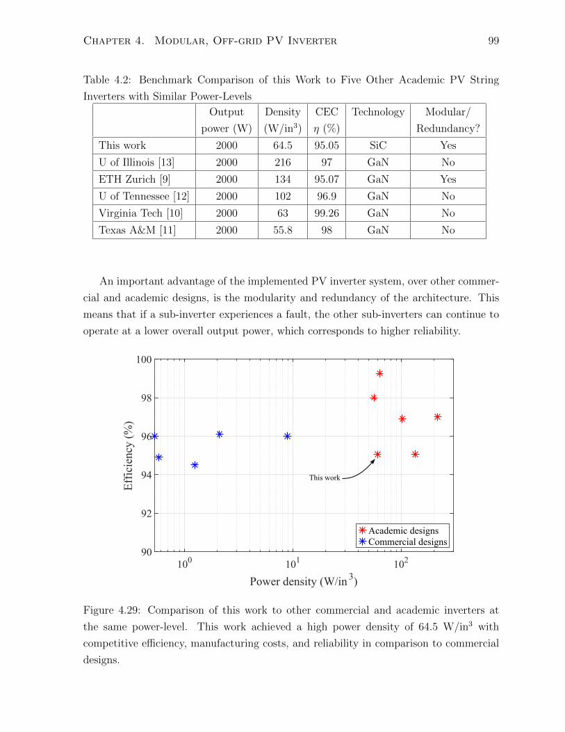
Chapter 4. Modular, Off-grid PV Inverter 99
Table 4.2: Benchmark Comparison of this Work to Five Other Academic PV String
Inverters with Similar Power-Levels
Output Density CEC Technology Modular/
power (W) (W/in3) η (%) Redundancy?
This work 2000 64.5 95.05 SiC Yes
U of Illinois [13] 2000 216 97 GaN No
ETH Zurich [9] 2000 134 95.07 GaN Yes
U of Tennessee [12] 2000 102 96.9 GaN No
Virginia Tech [10] 2000 63 99.26 GaN No
Texas A&M [11] 2000 55.8 98 GaN No
An important advantage of the implemented PV inverter system, over other commer-
cial and academic designs, is the modularity and redundancy of the architecture. This
means that if a sub-inverter experiences a fault, the other sub-inverters can continue to
operate at a lower overall output power, which corresponds to higher reliability.
100 101 102
Power density (W/in 3)
90
92
94
96
98
100
Effic
ienc
y (%
)
Academic designsCommercial designs
This work
Figure 4.29: Comparison of this work to other commercial and academic inverters at
the same power-level. This work achieved a high power density of 64.5 W/in3 with
competitive efficiency, manufacturing costs, and reliability in comparison to commercial
designs.

Chapter 4. Modular, Off-grid PV Inverter 100
4.3 Chapter Summary
This chapter presented the design of a modular, high power density off-grid inverter rated
at 2 kW. The inverter consists of 3 sub-inverters that work in parallel to supply the total
single-phase ac power. This modular approach enables sub-inverter-shedding at light
loads to improve efficiency as well as a very compact mechanical integration resulting in
a power density of 64.5 W/in3. The measured CEC efficiency of the inverter is 95.05%
and the average THD is 4.2%. The work presented in this chapter has been published
in [14].

References
[1] “Specification for radio disturbance and immunity measuring apparatus and meth-
ods - Part 1-2: Radio disturbance and immunity measuring apparatus - Coupling
devices for conducted disturbance measurements,” Canadian Standards Association,
Ontario, Canada, Standard, Mar. 2014.
[2] A. Costabeber, P. Mattavelli, and S. Saggini, “Digital time-optimal phase shedding
in multiphase buck converters,” IEEE Transactions on Power Electronics, vol. 25,
no. 9, pp. 2242–2247, Sept 2010.
[3] J. T. Su and C. W. Liu, “A novel phase-shedding control scheme for improved light
load efficiency of multiphase interleaved dc-dc converters,” IEEE Transactions on
Power Electronics, vol. 28, no. 10, pp. 4742–4752, Oct 2013.
[4] “Ce+t power - modular inverter,” CE+T Inverter Datasheet, available
https://assets-cf.ecopowersupplies.com/assets/files/30/92/cet-power-bravo-ac-
modular-inverter-230vac-datasheet.pdf.
[5] “Sma solar technology ag,” SMA Boy Storage 2.5 Datasheet, available
http://files.sma.de/dl/28035/SBS25-DEN1710-V21web.pdf.
[6] “Fronius inverters for small self-consumption systems,” Fronius Galvo 2.0-
1 Datasheet, available http://www.fronius.com/en/photovoltaics/products/all-
products/inverters/fronius-galvo/fronius-galvo-2-0-1.
[7] “Mitsubishi solar solutions,” EnaSolar 3.0 Datasheet, available
http://www.mitsubishi-electric.co.nz/materials/solar/brochures/EnaSolar GTInverter.pdf.
[8] “Abb solar string inverters,” ABB PVI-3.0 Datasheet, avail-
able https://search-ext.abb.com/library/Download.aspx Documen-
tID=9AKK106103A4852&LanguageCode=en&DocumentPartId=&Action=Launch.
101

REFERENCES 102
[9] D. Bortis, D. Neumayr, and J. W. Kolar, “Pareto optimization and comparative
evaluation of inverter concepts considered for the google little box challenge,” in 2016
IEEE 17th Workshop on Control and Modeling for Power Electronics (COMPEL),
June 2016, pp. 1–5.
[10] L. Zhang, R. Born, X. Zhao, and J. S. Lai, “A high efficiency inverter design for
google little box challenge,” in 2015 IEEE 3rd Workshop on Wide Bandgap Power
Devices and Applications (WiPDA), Nov 2015, pp. 319–322.
[11] A. S. Morsy, M. Bayern, and P. Enjeti, “High power density single phase inverter
using gan fets and active power decoupling for google little box challenge,” in 2015
IEEE 3rd Workshop on Wide Bandgap Power Devices and Applications (WiPDA),
Nov 2015, pp. 323–327.
[12] C. Zhao, B. Trento, L. Jiang, E. A. Jones, B. Liu, Z. Zhang, D. Costinett, F. F. Wang,
L. M. Tolbert, J. F. Jansen, R. Kress, and R. Langley, “Design and implementation of
a gan-based, 100-khz, 102-w/in3 single-phase inverter,” IEEE Journal of Emerging
and Selected Topics in Power Electronics, vol. 4, no. 3, pp. 824–840, Sept 2016.
[13] Y. Lei, C. Barth, S. Qin, W. c. Liu, I. Moon, A. Stillwell, D. Chou, T. Foulkes,
Z. Ye, Z. Liao, and R. C. N. Pilawa-Podgurski, “A 2 kw, single-phase, 7-level, gan
inverter with an active energy buffer achieving 216 w/in3 power density and 97.6%
peak efficiency,” in 2016 IEEE Applied Power Electronics Conference and Exposition
(APEC), March 2016, pp. 1512–1519.
[14] S. Chung, M. Nasr, D. Guirguis, M. Otsuka, S. Poshtkouhi, D. K. W. Li, V. Pala-
niappan, D. Romero, C. Amon, R. Orr, and O. Trescases, “Thermal and electrical
co-design of a modular high-density single-phase inverter using wide-bandgap de-
vices,” in 2016 IEEE Applied Power Electronics Conference and Exposition (APEC),
March 2016, pp. 1350–1357.

Chapter 5
Conclusions
5.1 Thesis Outcomes and Contributions
The work presented in this thesis is focused on increasing the power density of single-
phase inverters by utilizing SiC semiconductors, novel current mode control schemes,
modular architectures, active power decoupling techniques, and electrical and mechanical
co-designs. The main contributions of this thesis are listed below:
1. A hybrid Hysteretic Current-Mode Control (HCMC) scheme for single-phase in-
verters is proposed, simulated, and experimentally verified. This operating mode
combines the soft-switching benefits of Boundary Conduction Mode (BCM) with
the low inductor core loss benefits of Continuous Conduction Mode (CCM) in every
AC line cycle by operating in BCM near the zero crossings and transitioning into
CCM at the line cycle peaks and troughs. With higher switching frequencies en-
abled by SiC devices, and a lower peak inductor current due to the hybrid HCMC
control, inductors with lower inductance and saturation currents can be designed,
corresponding to smaller size and volume.
2. A modular design approach was taken to design and build a high power density
off-grid single-phase inverter for PV applications. The rated 2 kW output power is
equally shared among three separate single-phase sub-inverters connected in paral-
lel. This technique enables more efficient space utilization, thermal management,
and provides extra redundancy to increase reliability in the case that a single sub-
inverter fails. Each sub-inverter can be turned off, in a process known as sub-
inverter-shedding, to improve light load efficiency ad THD.
3. A novel Active Power Decoupling (APD) topology and control scheme is proposed,
103

Chapter 5. Conclusions 104
simulated, and experimentally verified to reduce the dc bus capacitance by 90%
and the overall inverter volume by 17.6%. The ratio of bus to APD capacitance
was optimized for volume through a set of simulations. The proposed full-bridge
APD topology is exactly the same as the sub-inverter design, as a result, fits per-
fectly with the modularity of the inverter system. Higher conversion efficiency is
achievable by attaining ZVS turn-on for all four MOSFETs, as opposed to other
conventional APD topologies.
4. In reference to Electric Vehicle (EV) applications, a 6.6 kW bi-directional EV
power-hub is designed and implemented capable of operating in the Vehicle-to-
Grid (V2G), Grid-to-Vehicle (G2V), Vehicle-to-House (V2H), and a novel Vehicle-
to-Vehicle (V2V) operating mode. The focus of this part of the thesis is placed on
the V2V operating mode, in which the transfer of DC power between two power-
hubs through their Level-2 AC power ports is investigated. It is experimentally
shown that the peak efficiency of the power-hub is increased from 96.6% to 98.3%,
by operating in DC transfer mode for V2V operation, thus increasing the power
capability by 50%.
5. In the new V2V DC transfer mode, the high duty cycle operation of the power-
hub causes an imbalance in power dissipation among the full-bridge MOSFETs. A
solution to this undesirable problem is addressed and simulated, which involves a
bipolar DC link regulation. In this regulation method, the polarity of the DC link
node voltage between the two power-hubs is reversed at a very low frequency to
prevent the power-stage MOSFETs from reaching steady-state thermal equilibrium.
Simulation results proved a 16oC lower average and 17oC lower peak MOSFET
junction temperature by commutating the link voltage polarity at a frequency of 1
Hz.
5.2 Future Work
Some sections of the EV-power hub and the off-grid inverter remain for future completion,
including:
1. Implementing the thermal design for the EV power-hub and experimentally verify-
ing the bipolar Vlink regulation scheme. The final goal of this project is to close the
loop that links the dc-ac inverter stage with the dc-dc Dual-Active-Bridge (DAB)
stage and integrate the complete EV power-hub system in a second enclosure pro-
totype to be utilized in the actual EV pick-up truck.

Chapter 5. Conclusions 105
2. Operating the off-grid PV inverter inside the enclosure and performing efficiency,
THD, and thermal measurements in a more realistic scenario. Operating the APD
module with the sub-inverters is also an important milestone in the future. By
implementing a Proportional-Resonant (PR) compensator, improvements to the
inverter voltage-loop is necessary to enhance the transient load handling capabili-
ties.
Related Documents