TECHNICAL NOTE High-performance Regulator IC Series for PCs Switching Regulators for DDR-SDRAM Cores BD9533EKN ●Description BD9533EKN is a switching regulator controller with high output current which can achieve low output voltage (0.7V to 2.0V) from a wide input voltage range (4.5V to 28V). High efficiency for the switching regulator can be realized by utilizing an external N-MOSFET power transistor. A new technology called H 3 Reg TM is a Rohm proprietary control method to realize ultra high transient response against load change. SLLM (Simple Light Load Mode) technology is also integrated to improve efficiency in light load mode, providing high efficiency over a wide load range. For protection and ease of use, the soft start function, variable frequency function, short circuit protection function with timer latch, over voltage protection function and REF synchronous function are all built in. This switching regulator is specially designed for the DDR-SDRAM core. ●Features 1) H 3 Reg TM Switching Regulator Controller 2) Light Load Mode and Continuous Mode Changeable 3) Thermal Shut Down (TSD), Under Voltage LockOut (UVLO), Over Current Protection (OCP), Over Voltage Protection (OVP), Short Circuit Protection (SCP) built-in 4) Soft start function to minimize rush current during startup 5) Switching Frequency Variable (f=200KHz~600KHz) 6) HQFN20V Package ●Applications Laptop PC, Desktop PC, LCD-TV, Digital Components Sep. 2008

Welcome message from author
This document is posted to help you gain knowledge. Please leave a comment to let me know what you think about it! Share it to your friends and learn new things together.
Transcript
TECHNICAL NOTE
High-performance Regulator IC Series for PCs
Switching Regulators for DDR-SDRAM Cores BD9533EKN
Description
BD9533EKN is a switching regulator controller with high output current which can achieve low output voltage (0.7V to 2.0V)
from a wide input voltage range (4.5V to 28V). High efficiency for the switching regulator can be realized by utilizing an
external N-MOSFET power transistor. A new technology called H3RegTM is a Rohm proprietary control method to realize
ultra high transient response against load change. SLLM (Simple Light Load Mode) technology is also integrated to improve
efficiency in light load mode, providing high efficiency over a wide load range. For protection and ease of use, the soft start
function, variable frequency function, short circuit protection function with timer latch, over voltage protection function and
REF synchronous function are all built in. This switching regulator is specially designed for the DDR-SDRAM core.
Features
1) H3RegTM Switching Regulator Controller
2) Light Load Mode and Continuous Mode Changeable
3) Thermal Shut Down (TSD), Under Voltage LockOut (UVLO), Over Current Protection (OCP),
Over Voltage Protection (OVP), Short Circuit Protection (SCP) built-in
4) Soft start function to minimize rush current during startup
5) Switching Frequency Variable (f=200KHz~600KHz)
6) HQFN20V Package
Applications
Laptop PC, Desktop PC, LCD-TV, Digital Components
Sep. 2008

2/20
Maximum Absolute Ratings (Ta=25) Parameter Symbol Limit Unit
Input Voltage 1 VCC 7 *1 VInput Voltage 2 VDD 7 *1 VInput Voltage 3 VIN 30 *1 VBOOT Voltage BOOT 35 *1 VBOOT-SW Voltage BOOT-SW 7 *1 VHG-SW Voltage HG-SW 7 *1 VLG Voltage LG VDD VREF Voltage REF VCC VOutput Voltage VOUT/Is+/Is- VCC VILIM/SCP/SS/FS/SLLM Voltage ILIM/SCP/SS/FS/SLLM VCC VVREG Voltage VREG VCC VEN Input Voltage EN 7 *1 VPower Dissipation 1 Pd1 0.5 *2 WPower Dissipation 2 Pd2 0.75 *3 WPower Dissipation 3 Pd3 1.75 *4 WPower Dissipation 4 Pd4 2.00 *5 WOperating Temperature Range Topr -10~+100 Storage Temperature Range Tstg -55~+150 Maximum Junction Temperature Tjmax +150 *1 Not to exceed Pd. *2 Reduced by 4mW for each increase in Ta of 1 over 25 (when don’t mounted on a heat radiation board ) *3 Reduced by 6mW for increase in Ta of 1 over 25. (when mounted on a board 70.0mm×70mm×1.6mm Glass-epoxy PCB.) *4 Reduced by 14mW for increase in Ta of 1 over 25. (when mounted on a board 70.0mm×70mm×1.6mm Glass-epoxy PCB.) *5 Reduced by 16mW for increase in Ta of 1 over 25. (when mounted on a board 70.0mm×70mm×1.6mm Glass-epoxy PCB.)
Operating Conditions (Ta=25)
Parameter Symbol MIN MAX Unit Input Voltage 1 VCC 4.5 5.5 V Input Voltage 2 VDD 4.5 5.5 V Input Voltage 3 VIN 4.5 28 V BOOT Voltage BOOT 4.5 33 V SW Voltage SW -0.7 28 V BOOT-SW Voltage BOOT-SW 4.5 5.5 V SLLM Input Voltage SLLM 0 5.5 V EN Input Voltage EN 0 5.5 V Output setting voltage REF 0.7 2.0 V Is Input Voltage Is+/Is- 0.7 2.7 V MIN ON Time Tonmin - 200 nsec
This product should not be used in a radioactive environment.

3/20
ELECTRICAL CHARACTERISTICS
(unless otherwise noted, Ta=25 VCC=5V,VDD=5V,EN/SLLM=5V,VIN=12V,REF=1.8V,RFS=68kΩ)
Parameter Symbol Standard Value
Unit Condition MIN TYP MAX
[Whole Device] VCC Bias Current Icc - 700 900 μA VIN Bias Current Iin - 100 200 μA VCC Standby Current Iccstb - 0 10 μA EN=0V VIN Standby Current Iinstb - 100 200 μA EN=0V EN Low Voltage Enlow GND - 0.8 V EN HighVoltage Enhigh 2.3 - 5.5 V EN Bias Current Ien - 7 10 μA
VREG Voltage Vreg 2.475 2.500 2.525 V Ireg=100μA Ta=-10 to 100*
[Under Voltage Locked Out ] VCC threshold voltage Vcc_UVLO 4.1 4.3 4.5 V VCC:Sweep up VCC hysteresis voltage dVcc_UVLO 100 160 220 mV VCC:Sweep down VIN threshold voltage Vin_UVLO 4.1 4.3 4.5 V VIN:Sweep up VIN hysteresis voltage dVin_UVLO 100 160 220 mV VIN:Sweep down VREG threshold voltage Vreg_UVLO 2.0 2.2 2.4 V VREG:Sweep up VREG hysteresis voltage dVreg_UVLO 100 160 220 mV VREG:Sweep down [H3RegTM] Frequency Fosc - 300 - kHz ON Time Ton 400 500 600 nsec MAX ON Time Tonmax - 3 - μsec MIN OFF Time Toffmin - 450 550 nsec [FET Driver] HG Higher side ON resistor HGhon - 3.0 6.0 Ω HG Lower side ON resistor HGlon - 2.0 4.0 Ω LG Higher side ON resistor LGhon - 2.0 4.0 Ω LG Lower side ON resistor LGlon - 0.5 1.0 Ω [Dead Time] HG rising HGdead - 50 - nsec LG rising LGdead - 50 - nsec [SCP] SCP Detect Voltage Vscp REF×0.65 REF×0.7 REF×0.75 V SCP threshold voltage Vscpth 1.2 1.25 1.3 V Charge current Iscp 1.5 2 2.5 μA Standby voltage Vscp_stb - - 50 mV [OVP] OVP Detect Voltage VOVP REF×1.16 REF×1.2 REF×1.24 V [Soft start] Charge current Iss 1.5 2 2.5 μA Standby voltage Vss_stb - - 50 mV [Over Current Protection Block]
Current limit threshold1 Ilim1 43 50 57 mVILIM=0.5V Ta=-10 to 100*
Current limit threshold2 Ilim2 160 200 240 mV ILIM=2.0V Reverse current limit threshold1 ReIlim1 - -50 - mV ILIM=0.5V Reverse current limit threshold2 ReIlim2 - -200 - mV ILIM=2.0V [VOUT setting ] VOUT offset voltage1 Voutoff1 REF-7m REF REF+7m V Ta=-10 to 100* VOUT bias current Ivout -100 0 100 nA REF bias current Iref -100 0 100 nA Is+ Input current IIs+ -1 0 1 μA Is+=1.8V Is- Input current IIs- -1 0 1 μA Is-=1.8V [SLLM ] Continuous mode threshold Vthcon VCC-0.5 - VCC V SLLM threshold VthSLLM GND - 0.5 V
* Design Guarantee

4/20
Reference Data
0
200
400
600
800
1000
1200
5 10 15 20 25
VIN [V]
TO
N [
nse
c]
0
50
100
150
200
250
300
350
400
0.6 0.8 1 1.2 1.4 1.6 1.8 2
REF [V]
TO
N [
nsec
]
0
100
200
300
400
500
600
0.6 0.8 1 1.2 1.4 1.6 1.8 2
REF [V]
TO
N [
nsec
]
0
100
200
300
400
500
600
700
800
900
1000
0.6 0.8 1 1.2 1.4 1.6 1.8 2
REF [V]
TO
N [
nsec
]
-3
-2
-1
0
1
2
3
-10 10 30 50 70 90
Ta []
VO
UT
-RE
F [m
V]
Fig.1 Ta vs Icc Fig.3 Ta vs UVLO (VCC)
Fig.4 Ta vs UVLO (VIN) Fig.5 Ta vs UVLO (VREG) Fig.6 Ta vs EN Threshold
Fig.7 VCC vs VREG (Start up) Fig.8 REF vs ON TIME (VIN=7V)
Fig.9 REF vs ON TIME (VIN=12V)
Fig.10 REF-ON TIME (VIN=25V)
Fig.11 VIN-ON TIME (REF=1.8V)
550
560
570
580
590
600
-10 10 30 50 70 90Ta()
Icc
(uA
)
2.490
2.492
2.494
2.496
2.498
2.500
-10 10 30 50 70 90Ta()
VR
EG
[V]
4.00
4.05
4.10
4.15
4.20
4.25
4.30
-10 10 30 50 70 90Ta()
VC
C[V
]
4.00
4.05
4.10
4.15
4.20
4.25
4.30
-10 10 30 50 70 90Ta()
VIN
[V]
1.90
1.95
2.00
2.05
2.10
2.15
2.20
-10 10 30 50 70 90Ta()
VR
EG
[V]
1.2
1.3
1.4
1.5
1.6
1.7
-10 10 30 50 70 90Ta()
EN
[V]
0.0
0.4
0.8
1.2
1.6
2.0
2.4
2.8
0 1.5 3 4.5 6Vcc(V)
VR
EG
(V)
Sweep up
Sweep down
Fig.12 Ta vs VOUT offset
Fig.2 Ta vs VREG
Top: -10Middle: 25
Bottom: 100
Top: -10Middle: 25
Bottom: 100Right: -10Middle: 25
Left: 100
Top: -10Middle: 25
Bottom: 100
Top: -10Middle: 25
Bottom: 100
Sweep up
Sweep down
Sweep up
Sweep down
Sweep up
Sweep down

5/20
Reference Data
46
48
50
52
54
-10 10 30 50 70 90Te []
⊿Is
[m
V]
Fig.14 Ta vs Frequency Fig.15 VIN vs Frequency
Fig.16 Io vs Efficiency (VIN=7V)
Fig.17 Io vs Efficiency (VIN=12V)
Fig.18 Io vs Efficiency (VIN=20V)
Fig.19 Load Transient Response (VIN=7V)
Fig.20 Load Transient Response (VIN=12V)
Fig.21 Load Transient Response (VIN=19V)
250
270
290
310
330
350
-10 10 30 50 70 90Ta()
freq
uenc
y[kH
z]
200
240
280
320
360
400
0 5 10 15 20 25VIN(V)
fre
quen
cy[k
Hz]
0
20
40
60
80
100
1 10 100 1000 10000Io(mA)
η[%
]
0
20
40
60
80
100
1 10 100 1000 10000Io(mA)
η[%
]
0
20
40
60
80
100
1 10 100 1000 10000Io(mA)
η[%
]
Io=2A
Io=0A
SLLM
Continuous mode
VOUT
HG/LG
IOUT
VOUT
HG/LG
IOUT
VOUT
HG/LG
IOUT
Fig.13 Ta vs current limit threshould
ILIM=0.5V
Fig.22 Load Transient Response (VIN=7V)
Fig.23 Load Transient Response (VIN=12V)
Fig.24 Load Transient Response (VIN=19V)
VOUT
HG/LG
IOUT
VOUT
HG/LG
IOUT
VOUT
HG/LG
IOUT
SLLMSLLM
Continuous mode
Continuous mode
6/20
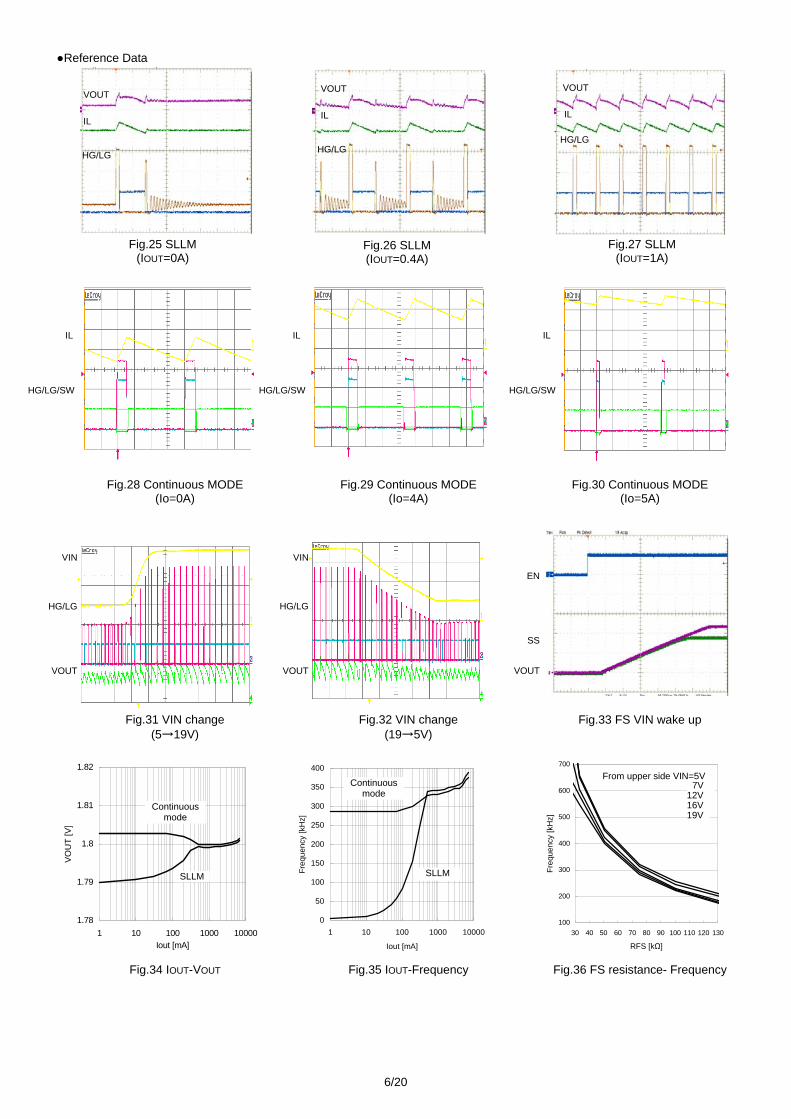
Reference Data
100
200
300
400
500
600
700
30 40 50 60 70 80 90 100 110 120 130
RFS [kΩ]
Fre
quen
cy [
kHz]
Fig.25 SLLM (IOUT=0A)
Fig.26 SLLM (IOUT=0.4A)
Fig.27 SLLM (IOUT=1A)
1.78
1.79
1.8
1.81
1.82
1 10 100 1000 10000Iout [mA]
VO
UT
[V]
0
50
100
150
200
250
300
350
400
1 10 100 1000 10000
Iout [mA]
Fre
qu
en
cy [
kHz]
VOUT
IL
HG/LG
VOUT
IL
HG/LG
VOUT
IL
HG/LG
Continuous mode
SLLM SLLM
From upper side VIN=5V7V
12V16V19V
Continuous mode
Fig.31 VIN change (5→19V)
Fig.32 VIN change (19→5V)
Fig.33 FS VIN wake up
Fig.34 IOUT-VOUT Fig.35 IOUT-Frequency Fig.36 FS resistance- Frequency
Fig.28 Continuous MODE (Io=0A)
Fig.29 Continuous MODE (Io=4A)
Fig.30 Continuous MODE (Io=5A)
HG/LG
VOUT
VIN
HG/LG
VOUT
VIN
HG/LG/SW
IL
HG/LG/SW
IL
HG/LG/SW
IL
EN
SS
VOUT
7/20
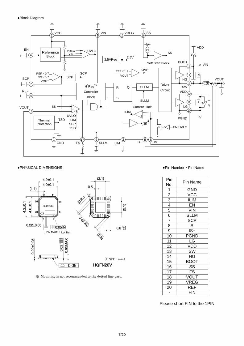
Block Diagram
PHYSICAL DIMENSIONS Pin Number・Pin Name
Please short FIN to the 1PIN
PinNo.
Pin Name
1 GND 2 VCC 3 ILIM 4 EN 5 VIN 6 SLLM 7 SCP 8 IS- 9 IS+
10 PGND 11 LG 12 VDD 13 SW 14 HG 15 BOOT 16 SS 17 FS 18 VOUT 19 VREG 20 REF - FIN
Reference Block
Thermal Protection
H3RegTM
Controller
Block
2.5VReg
SLLMR
S
Q
Driver
Circuit
GND FS ILIM Is+ Is- SLLM
PGND
LG
VDD
SW
HG
BOOT
SS VREGVIN VCC
SCP
REF
VOUT
TSD UVLO
ILIMSCPTSD
ILIM
Current Limit
-+
SLLM
2.5VSS
Soft Start Block
UVLO VREGVIN
SCPREF×0.7
SS×0.7VOUT
SCP
SS
2 5 19 16
4
7
20
18
1 17 3 9 86
15
14
13
12
11
10
VDD
VIN
VOUT
++
REF×1.2
VOUT
OVP
EN/UVLO
EN
(UNIT:mm)
HQFN20V
BD9533
1PIN MARK Lot No.
※ Mounting is not recommended to the dotted line part.

8/20
Pin Descriptions
・GND(1pin)
This is the ground pin for IC internal circuits. It is equivalent to FIN voltage. ・VCC(2pin)
This is the power supply pin for IC internal circuits, except the FET driver. The maximum circuit current is 900uA. The input
supply voltage range is 4.5V to 5.5V. It is recommended that a 0.1uF bypass capacitor be put in this pin.
・ILIM(3pin) BD9533EKN detects the voltage between Is+ pin and Is- pin and limits the output current (OCP). Voltage equivalent to 1/10 of the ILIM voltage is the voltage drop of external current sense resistor. A very low current sense resistor or inductor DCR can also be used for this platform.
・EN(4pin) When EN pin voltage is at least 2.3V, the status of this switching regulator becomes active. Conversely, the status switches off when EN pin voltage goes lower than 0.8V and circuit current becomes 10uA.
・VIN(5pin) The duty cycle is determined by input voltage and output voltage. In other words, the output voltage is affected by input voltage. Therefore, when VIN voltage fluctuates, the output voltage becomes also unstable. Since the VIN line is also the input voltage of the switching regulator, stability depends on the impedance of the voltage supply. It is recommended to establish a bypass capacitor or CR filter suitable for the actual application.
・SLLM(6pin) This is the switch shift pin for Simple Light Load Mode. The efficiency in SLLM is improved when SLLM pin voltage goes lower than 0.5V.
・SCP(7pin) This is the pin to adjust the timer latch time for short circuit protection. The timer circuit is active when the pin voltage becomes 70% of REF, and the output switches OFF and latched after the specified time. When the UVLO circuit is active or EN is low, this latch function is cancelled.
・Is-(8pin) ,Is+(9pin) These pins are connected to both sides of the current sense resistor to detect output current. The voltage drop between Is+ and Is- is compared with the voltage equivalent to 1/10 of ILIM voltage. When this voltage drop reaches the specified voltage level, the output voltage goes OFF.
・PGND(10pin) This is the power ground pin connected to the source of the low side FET.
・LG(11pin) This is the voltage supply to drive the Gate of the low side FET. This voltage swings between VDD and PGND. High-speed Gate driving for the low side FET is achieved due to the low on-resistance (2 ohm when LG is high, 0.5 ohm when LG is low) of the driver.
・VDD(12pin) This is the power supply pin to drive the LOW side FET. It is recommended that a 1uF bypass capacitor be established to compensate for rush current during the FET ON/OFF transition.
・SW(13pin) This is the source pin for the high side FET. The maximum absolute ratings are 30V (from GND). SW voltage swings between VIN and GND.
・HG(14pin) This is the voltage supply to drive the Gate of the high side FET. This voltage swings between BOOT and SW. High-speed Gate driving for the high side FET is achieved due to the low on-resistance (3 ohm when HG is high, 2 ohm when HG is low) of the driver.
・BOOT(15pin) This is the voltage supply to drive the high side FET. The maximum absolute ratings are 35V (from GND) and 7V (from SW). BOOT voltage swings between VIN+Vcc and Vcc during active operation.
・SS(16pin) This is the adjustment pin to set the soft start time. SS voltage is low during standby status. When EN is ON, the soft start time can be determined by the SS charge current and capacitor between SS-GND. Until SS reaches REF voltage, the output voltage is equivalent to SS voltage.
・FS(17pin) This is the pin to adjust the switching frequency based on the resistor value. The frequency range is f=200KHz - 600KHz.
・VOUT(18pin) This is the output voltage sense pin. It is also possible to adjust the output voltage using external resistor divider based on the equation, REF≒VOUT.
・VREG(19pin) This is the reference voltage output pin. The voltage is 2.5V, with 100uA current ability. It is recommended that a 1uF capacitor (X5R or X7R) be established between VREG and GND. When REF is not adjusted from the external voltage supply, the REF voltage can be adjusted using the external resistor divider of VREF.
・REF(20pin) This is the output voltage adjustment pin. It is very convenient for synchronizing external voltage supply. The IC controls the output voltage (REF≒VOUT).

9/20
Explanation of Operation
The BD9533EKN is a synchronous buck regulator controller incorporating ROHM’s proprietary H3RegTM CONTROLLA control
system. When VOUT drops due to a rapid load change, the system quickly restores VOUT by extending the TON time interval.
Thus, it serves to improve the regulator’s transient response. Activating the Light Load Mode will also exercise Simple Light
Load Mode (SLLM) control when the load is light, to further increase efficiency.
H3RegTM control
(Normal operation)
(VOUT drops due to a rapid load change)
(SLLM )
VOUT
REF
HG
LG
HG output is determined with the formula above. LG outputs until the status of VOUT is lower than REFafter the status of HG is off.
When VOUT falls to a threshold voltage (REF), the drop is
detected, activating the H3RegTM CONTROLLA system.
VOUT
REF
HG
Io
LG
TON+α
When VOUT drops due to a rapid load change, and
the voltage remains below REF after the
programmed TON time interval has elapsed, the
system quickly restores VOUT by extending the TON
time, improving the transient response.
TON=REF
VIN ×
1
f [sec]・・・(1)
In SLLM (SLLM=0V), SLLM function is operated whenLG pin is OFF and the coil current is lower than 0A(the current goes from VOUT to SW). And it stops tooutput next HG. When VOUT goes lower than REF voltage again, thestatus of HG is ON.
VOUT
REF
HG
LG
0A

10/20
Timing Chart
• Soft Start Function
・Timer Latch Type Short Circuit Protection
・Over Voltage Protection
VOUT
HG
LG
REF×1.2
Switching
VOUT
SCP
EN/UVLO
TSCP
REF×0.7
EN
SS
VOUT
IIN
TSS
Soft start time
Tss= REF×Css
2μA(typ) [sec]
Incoming current
IIN= Co×VOUT
Tss [A]
Short protection time setting
Tscp=1.25(V)×CSCP
2μA(typ) [sec]
Soft start is exercised with the EN pin set high. Current
control takes effect at startup, enabling a moderate
output voltage “ramping start.” Soft start timing and
incoming current are calculated with formulas (2) and
(3) below.
Short protection kicks in when output falls to or below
REF X 0.7. When the programmed time period elapses,
output is latched OFF to prevent destruction of the IC.
Output voltage can be restored either by reconnecting
the EN pin or disabling UVLO. Short circuit protection
time is programmed using formula (4) below.
(Css: Soft start capacitor; Co: Output capacitor)
・・・(2)
・・・(3)
・・・(4)

11/20
External Component Selection
1. Inductor (L) selection
※Passing a current larger than the inductor’s rated current will cause magnetic saturation in the inductor and decrease
system efficiency. In selecting the inductor, be sure to allow enough margin to assure that peak current does not exceed the
inductor rated current value.
※To minimize possible inductor damage and maximize efficiency, choose a inductor with a low (DCR, ACR) resistance.
2.Output Capacitor (CO) Selection
Please give due consideration to the conditions in formula (9) below for output capacity, bearing in mind that output rise time
must be established within the soft start time frame.
Note: Improper capacitor may cause startup malfunctions.
3. Input Capacitor (Cin) Selection
A low ESR capacitor is recommended to reduce ESR loss and maximize efficiency.
The inductor value is a major influence on the output ripplecurrent. As formula (5) below indicates, the greater the inductor orthe switching frequency, the lower the ripple current.
ΔIL=(VIN-VOUT)×VOUT
ΔIL×VIN×f[A]・・・(5)
The proper output ripple current setting is about 30% of maximumoutput current.
ΔIL=0.3×IOUTmax. [A]・・・(6)
L=(VIN-VOUT)×VOUT
ΔIL×VIN×f [H]・・・(7)
(ΔIL: output ripple current; f: switch frequency)
When determining the proper output capacitor, be sure to factor in the equivalentseries resistance required to smooth out ripple volume and maintain a stableoutput voltage range. Output ripple voltage is determined as in formula (8) below.
ΔVOUT=ΔIL×ESR+ESL×ΔIL/TON [V]・・・(8)
(ΔIL: Output ripple current; ESR: CO equivalent series resistance, ESR:equivalent series inductance)
※ In selecting a capacitor, make sure the capacitor rating allows sufficientmargin relative to output voltage. Note that a lower ESR can minimize outputripple voltage.
Co≦ Tss×(Limit-IOUT)
VOUT ・・・(9)
Tss: Soft start time Limit: Over current detection
Input Capacitor
The input capacitor selected must have low enough ESR resistance to fullysupport large ripple output, in order to prevent extreme over current. The formulafor ripple current IRMS is given in (10) below.
IRMS=IOUT× VOUT(VIN-VOUT)
VIN [A]・・・(10)
√
Where VCC=2×VOUT, IRMS=IOUT
2
ΔIL
VIN
IL
L
Co
VOUT
Output ripple current
VIN
L Co
VOUT
Cin
VIN
L
Co
VOUT
ESR
Output capacitor
ESL

12/20
4. MOSFET Selection
5. Setting Detection Resistance
Pmain=PRON+PGATE+PTRAN
Psyn=PRON+PGATE
VOUT
VIN×RON×IOUT
2+Ciss×f×VDD+ VIN
2×Crss×IOUT×f
IDRIVE
VIN-VOUT
VIN×RON×IOUT
2+Ciss×f×VDD
The over current protection function detects the output ripplecurrent peak value. This parameter (setting value) isdetermined as in formula (13) below.
VILIM×0.1
R ILMIT=
(VILIM: ILIM voltage; R: Detection resistance)
VIN
L
Co
VOUT
synchronous switch
main switch
VIN
L
Co
VOUT
Current limit
IL
R
Loss on the main MOSFET
(Ron: On-resistance of FET; Ciss: FET gate capacity; f: Switching frequency Crss: FET inverse transfer function; IDRIVE: Gate peak current)
Loss on the synchronous MOSFET
= ・・・(11)
= ・・・(12)
[A]・・・(13)
ILMIT=VILIM×0.1×
When the over current protection is detected by DCR of coil L, this parameter (setting value) is determined as in formula (14) below. (Application circuit:P20)
r×C
L
(VILIM:ILIM voltage RL: the DCR value of coil)
[A]・・・(14)
VIN
L
Co
VOUT
Current limit
IL
RL
r C L
r×C (RL= )
13/20
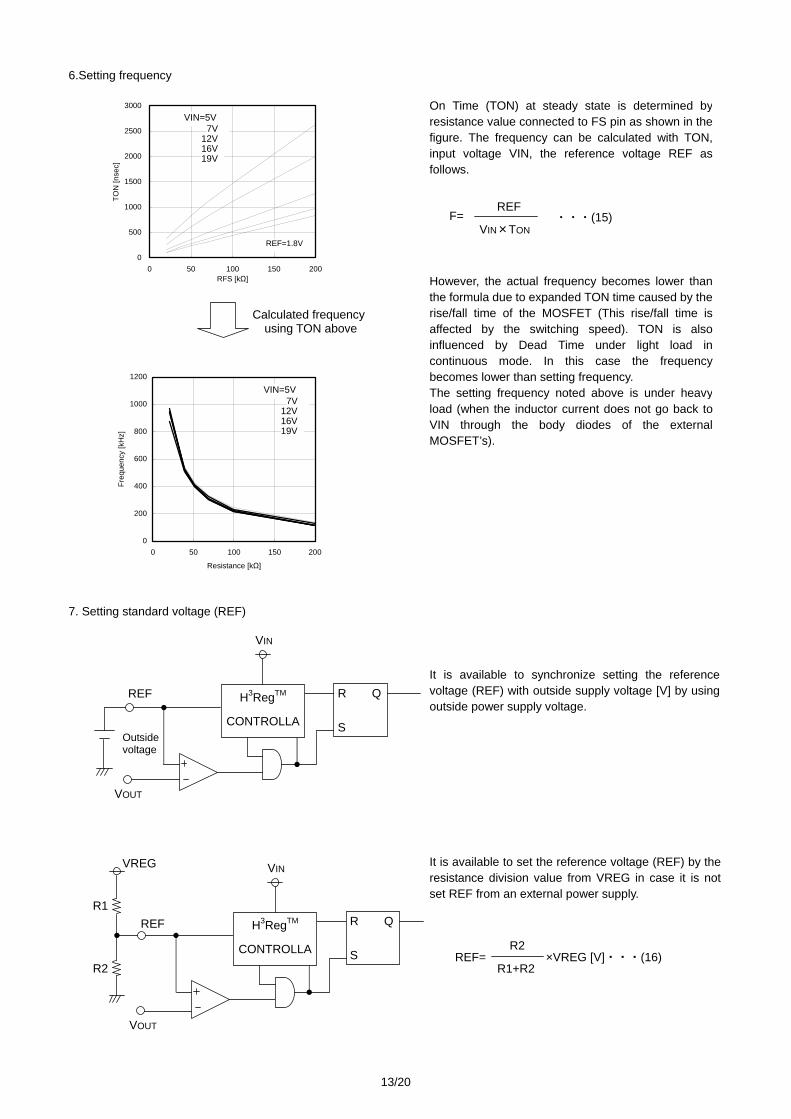
6.Setting frequency
7. Setting standard voltage (REF)
REF= ×VREG [V]・・・(16)
0
200
400
600
800
1000
1200
0 50 100 150 200
Resistance [kΩ]
Fre
quen
cy [
kHz]
It is available to set the reference voltage (REF) by theresistance division value from VREG in case it is notset REF from an external power supply.
VOUT
H3RegTM
CONTROLLA S
R Q
VIN VREG
R1
R2
REF
It is available to synchronize setting the referencevoltage (REF) with outside supply voltage [V] by usingoutside power supply voltage.
H3RegTM
CONTROLLA S
R Q
VIN
REF
R1+R2
R2
VOUT
Outside voltage
0
500
1000
1500
2000
2500
3000
0 50 100 150 200RFS [kΩ]
TO
N [
nsec
]VIN=5V
7V 12V 16V 19V
REF=1.8V
VIN=5V 7V
12V 16V 19V
F=REF
VIN×TON
Calculated frequency using TON above
On Time (TON) at steady state is determined byresistance value connected to FS pin as shown in thefigure. The frequency can be calculated with TON,input voltage VIN, the reference voltage REF asfollows. ・・・(15) However, the actual frequency becomes lower thanthe formula due to expanded TON time caused by therise/fall time of the MOSFET (This rise/fall time isaffected by the switching speed). TON is alsoinfluenced by Dead Time under light load incontinuous mode. In this case the frequencybecomes lower than setting frequency. The setting frequency noted above is under heavyload (when the inductor current does not go back toVIN through the body diodes of the externalMOSFET’s).
14/20
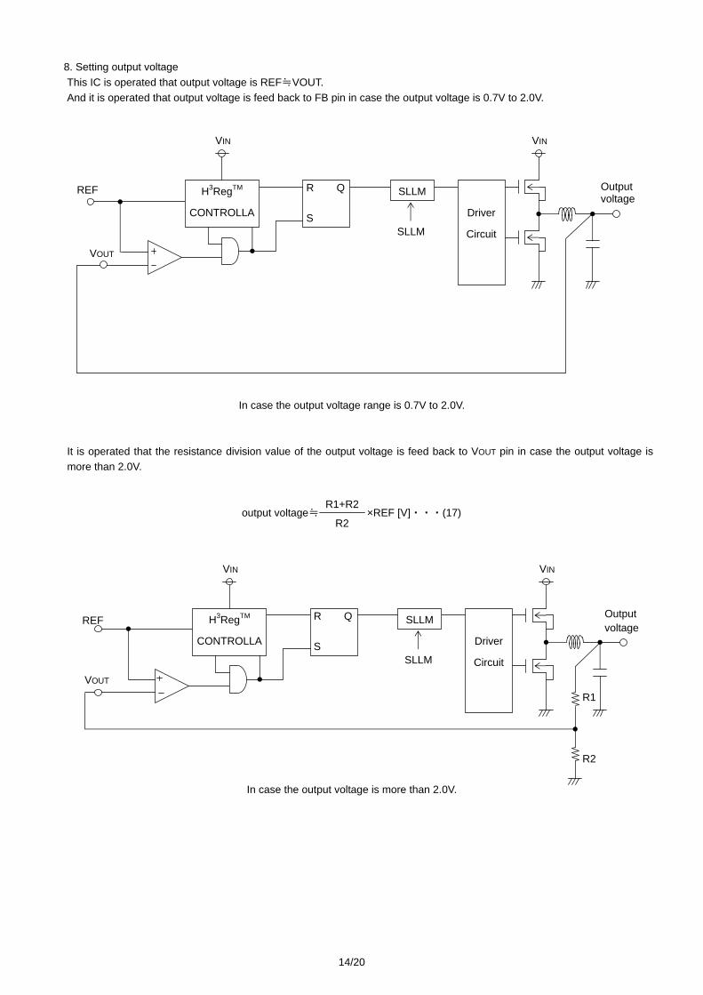
8. Setting output voltage
This IC is operated that output voltage is REF≒VOUT.
And it is operated that output voltage is feed back to FB pin in case the output voltage is 0.7V to 2.0V.
REF
In case the output voltage range is 0.7V to 2.0V.
It is operated that the resistance division value of the output voltage is feed back to VOUT pin in case the output voltage is
more than 2.0V.
output voltage≒ ×REF [V]・・・(17)
REF
R1
R2
In case the output voltage is more than 2.0V.
VOUT
H3RegTM
CONTROLLA S
R Q SLLM
Driver
CircuitSLLM
VIN
Output voltage
VIN
H3RegTM
CONTROLLA S
R Q SLLM
Driver
Circuit SLLM
VIN
Output voltage
VIN
VOUT
R1+R2
R2

15/20
I/O Equivalent Circuit
3pin (ILIM) 4pin (EN) 5pin (VIN)
6pin (SLLM) 7pin (SCP) 8pin (Is-)
9pin (Is+) 11pin (LG) 13pin (SW)
14pin(HG) 15pin (BOOT) 16pin (SS)
17pin (FS) 18pin (VOUT) 19pin (VREG)
20pin (REF)
VCC
VCC VCC VCC
VCC
VCC VDD
VCC BOOT HG
VCC VCC VCC
BOOT BOOT
HG SW
VCC

16/20
Evaluation Board Circuit (Frequency=300kHz application circuit in Continuous mode/SLLM)
Part No
Value Company Part name Part No
Value Company Part name
U1 ROHM BD9533EKN R4 Q1 ROHM RSS100N03 R5 0Ω ROHM MCR03 Q2 ROHM RSS100N03 R6 D1 ROHM RB521S-30 R7 5mΩ ROHM PMR100 D2 ROHM RB051L-40 R8 0Ω ROHM MCR03 C1 1uF KYOCERA CM105B105K06A R9 0Ω ROHM MCR03
C2 10nF MURATA GRM39X7R103K50 R10 0Ω ROHM MCR03 C3 100pF MURATA GRM39C0G101J50 R11 0Ω ROHM MCR03 C4 R12 200kΩ ROHM MCR03 C5 R13 51kΩ ROHM MCR03 C6 10uF KYOCERA CM21B106K06 R14 68kΩ ROHM MCR03 C7 R15 180kΩ ROHM MCR03 C8 0.1uF KYOCERA CM05B104K25A R16 1kΩ ROHM MCR03 C9 10uF KYOCERA CM316B106M16A R17 0Ω ROHM MCR03 C10 10uF KYOCERA CM316B106M16A R18 10kΩ ROHM MCR03 C11 1000pF MURATA GRM39X7R102K50 R19 10kΩ ROHM MCR03 C12 1500pF MURATA GRM39X7R152K50 R20 0Ω ROHM MCR03 C13 1uF KYOCERA CM105B105K06A R21 C14 R22 C15 10uF KYOCERA CM21B106M06A R23 0Ω ROHM MCR03 C16 R24 0Ω ROHM MCR03 C17 470uF SANYO 2R5TPE470ML R25 0Ω ROHM MCR03 R1 68KΩ ROHM MCR03 R26 R2 0Ω ROHM MCR03 L1 1.8uH SUMIDA CDEP104-1R8ML R3 0Ω ROHM MCR03
2.5V
0.5V
1.8V
11
C9
C1
0
R1
2
R18
R19
R9
R1
R1
6
R2
C1
5
R11
R8
C6
VREG
ILIM
REF
R1
3 R
20
R1
5 R
17
R1
4
C3
C1
4
C1
3
C1
C2
C11
C1
2 EN
SLLM
VCC
VIN
VCC
D1
Q1
Q2
R10
C8
D2
PGND
PGND PGND
C4
C5
PGNDPGND
C1
7
C1
6
R3
R5
PGND PGND
R7
R2
3
R2
4
R2
2
R2
1
R2
5 R
26
R6
L1
VIN
BD9533EKN PGND
GND
VOUT
R4
EN
SLLM
VREG
ILIM
REF
FS
SCP
SS
VCC
GND
VDD
BOOT
HG
Is-
SW
LG
PGND
Is+
VOUT
5
4
6
19
3
16
7
17
20
1
2
12
15
14
13
10
9
8
4.5V~25V
5V
1.8V/10A
18

17/20
Evaluation Board Circuit (Frequency=300kHz application circuit for detecting DCR current in Continuous mode/SLLM)
Evaluation Board Parts List
Part No
Value Company Part name Part No
Value Company Part name
U1 ROHM BD9533EKN R4 Q1 ROHM RSS100N03 R5 0Ω ROHM MCR03 Q2 ROHM RSS100N03 R6 1kΩ ROHM MCR03 D1 ROHM RB521S-30 R7 D2 ROHM RB051L-40 R8 0Ω ROHM MCR03 C1 1uF KYOCERA CM105B105K06A R9 0Ω ROHM MCR03
C2 10nF MURATA GRM39X7R103K50 R10 0Ω ROHM MCR03 C3 100pF MURATA GRM39C0G101J50 R11 0Ω ROHM MCR03 C4 R12 51kΩ ROHM MCR03 C5 R13 200kΩ ROHM MCR03 C6 10uF KYOCERA CM21B106K06 R14 68kΩ ROHM MCR03 C7 0.1uF KYOCERA CM05B104K25A R15 180kΩ ROHM MCR03 C8 0.1uF KYOCERA CM05B104K25A R16 1kΩ ROHM MCR03 C9 10uF KYOCERA CM316B106M16A R17 0Ω ROHM MCR03 C10 10uF KYOCERA CM316B106M16A R18 10kΩ ROHM MCR03 C11 1000pF MURATA GRM39X7R102K50 R19 10kΩ ROHM MCR03 C12 1500pF MURATA GRM39X7R152K50 R20 0Ω ROHM MCR03 C13 1uF KYOCERA CM105B105K06A R21 0Ω ROHM MCR03 C14 R22 0Ω ROHM MCR03 C15 10uF KYOCERA CM21B106M06A R23 C16 R24 C17 330uF SANYO 6TPB330M R25 0Ω ROHM MCR03 R1 68KΩ ROHM MCR03 R26 R2 0Ω ROHM MCR03 L1 3.3uH NEC/TOKIN MPLC0730L3R3 R3 0Ω ROHM MCR03
11
C9
C1
0
R1
2
R18
R19
R9
R1
R1
6
R2
C1
5
R11
R8
C6
VREG
ILIM
REF
R1
3 R
20
R1
5 R
17
R1
4
C3
C1
4
C1
3
C1
C2
C11
C1
2 EN
SLLM
VCC
VIN
VCC
D1
Q1
Q2
R10
C8
D2
PGND
PGND PGND
C4
C5
PGNDPGND
C1
7
C1
6
R3
R5
PGND PGND
R2
3
R2
4
R2
2
R2
1
R2
5 R
26
R6
L1
VIN
BD9533EKN PGND
GND
VOUT
R4
EN
SLLM
VREG
ILIM
REF
FS
SCP
SS
VCC
GND
VDD
BOOT
HG
Is-
SW
LG
PGND
Is+
VOUT
5
4
6
19
3
16
7
17
20
1
2
12
15
14
13
10
9
8
4.5V~25V
5V
C7
18

18/20
Operation Notes 1. Absolute maximum ratings
An excess in the absolute maximum ratings, such as supply voltage, temperature range of operating conditions, etc., can
break down the devices, thus making impossible to identify breaking mode, such as a short circuit or an open circuit. If any
over rated values will expect to exceed the absolute maximum ratings, consider adding circuit protection devices, such as
fuses.
2. Connecting the power supply connector backward
Connecting of the power supply in reverse polarity can damage IC. Take precautions when connecting the power supply
lines. An external direction diode can be added.
3. Power supply lines
Design PCB layout pattern to provide low impedance GND and supply lines. To obtain a low noise ground and supply line,
separate the ground section and supply lines of the digital and analog blocks. Furthermore, for all power supply terminals to
ICs, connect a capacitor between the power supply and the GND terminal. When applying electrolytic capacitors in the
circuit, not that capacitance characteristic values are reduced at low temperatures.
4. GND voltage
The potential of GND pin must be minimum potential in all operating conditions. 5. Thermal design
Use a thermal design that allows for a sufficient margin in light of the power dissipation (Pd) in actual operating conditions.
6. Inter-pin shorts and mounting errors Use caution when positioning the IC for mounting on printed circuit boards. The IC may be damaged if there is any connection error or if pins are shorted together.
7. Actions in strong electromagnetic field Use caution when using the IC in the presence of a strong electromagnetic field as doing so may cause the IC to malfunction.
8. ASO
When using the IC, set the output transistor so that it does not exceed absolute maximum ratings or ASO.
9. Thermal shutdown circuit
The IC incorporates a built-in thermal shutdown circuit (TSD circuit). The thermal shutdown circuit (TSD circuit) is designed
only to shut the IC off to prevent thermal runaway. It is not designed to protect the IC or guarantee its operation. Do not
continue to use the IC after operating this circuit or use the IC in an environment where the operation of this circuit is
assumed.
TSD on temperature [°C] (typ.) Hysteresis temperature [°C] (typ.) BD9533EKN 175 15
10. Testing on application boards When testing the IC on an application board, connecting a capacitor to a pin with low impedance subjects the IC to stress. Always discharge capacitors after each process or step. Always turn the IC's power supply off before connecting it to or removing it from a jig or fixture during the inspection process. Ground the IC during assembly steps as an antistatic measure. Use similar precaution when transporting or storing the IC.

19/20
11. Regarding input pin of the IC This monolithic IC contains P+ isolation and P substrate layers between adjacent elements in order to keep them isolated. P-N junctions are formed at the intersection of these P layers with the N layers of other elements, creating a parasitic diode or transistor. For example, the relation between each potential is as follows:
When GND > Pin A and GND > Pin B, the P-N junction operates as a parasitic diode. When GND > Pin B, the P-N junction operates as a parasitic transistor.
Parasitic diodes can occur inevitable in the structure of the IC. The operation of parasitic diodes can result in mutual
interference among circuits, operational faults, or physical damage. Accordingly, methods by which parasitic diodes
operate, such as applying a voltage that is lower than the GND (P substrate) voltage to an input pin, should not be used.
12. Ground Wiring Pattern When using both small signal and large current GND patterns, it is recommended to isolate the two ground patterns, placing a single ground point at the ground potential of application so that the pattern wiring resistance and voltage variations caused by large currents do not cause variations in the small signal ground voltage. Be careful not to change the GND wiring pattern of any external components, either.
Fig. 37 Example of IC structure
Resistor Transistor (NPN)
N
N N P+ P+ P
P substrate
GND Parasitic element
Pin A
N
N P+ P+ P
P substrate
GND Parasitic element
Pin B C
B
E
N
GND
Pin A
Parasitic element
Pin B
Other adjacent elements
E
B C
GND
Parasitic element

20/20
Type Designations (Selections) for Ordering
B D 9 5 3 3 K ― E 2 E
Product name Package type Taping type name E2= Embossed carrier tape
・BD9533
・EKN : HQFN20V
N
HQFN20V
(Unit:mm)
<Dimension>
4.2±0.1
(1.1)
0.22±0.05
4.0±
0.1
4.0±0.1
4.2±
0.1
20
16
15 11
10
6
51
0.05
0.95
MA
X
0.22
±0.0
5
0.05
0.02
+0.0
3−0
.02
(0.5)
3−(0.35)
(0.2
2)
0.5
(2.1
)
(2.1)
0.6 +0.1−0.3
(The direction is the 1pin of product is at the upper left when you hold reel on the left hand and you pull out the tape on the right hand)
Tape
Quantity
Direction of feed
Embossed carrier tape(with dry pack)
2500pcs E2
<Tape and Reel information>
※When you order , please order in times the amount of package quantity.
ReelDirection of feed
1pin
1234
1234
1234
1234
1234
1234
Catalog No.08T441A '08.9 ROHM ©

DatasheetDatasheet
Notice - GE Rev.002© 2014 ROHM Co., Ltd. All rights reserved.
Notice Precaution on using ROHM Products
1. Our Products are designed and manufactured for application in ordinary electronic equipments (such as AV equipment, OA equipment, telecommunication equipment, home electronic appliances, amusement equipment, etc.). If you intend to use our Products in devices requiring extremely high reliability (such as medical equipment (Note 1), transport equipment, traffic equipment, aircraft/spacecraft, nuclear power controllers, fuel controllers, car equipment including car accessories, safety devices, etc.) and whose malfunction or failure may cause loss of human life, bodily injury or serious damage to property (“Specific Applications”), please consult with the ROHM sales representative in advance. Unless otherwise agreed in writing by ROHM in advance, ROHM shall not be in any way responsible or liable for any damages, expenses or losses incurred by you or third parties arising from the use of any ROHM’s Products for Specific Applications.
(Note1) Medical Equipment Classification of the Specific Applications JAPAN USA EU CHINA
CLASSⅢ CLASSⅢ
CLASSⅡb CLASSⅢ
CLASSⅣ CLASSⅢ
2. ROHM designs and manufactures its Products subject to strict quality control system. However, semiconductor
products can fail or malfunction at a certain rate. Please be sure to implement, at your own responsibilities, adequate safety measures including but not limited to fail-safe design against the physical injury, damage to any property, which a failure or malfunction of our Products may cause. The following are examples of safety measures:
[a] Installation of protection circuits or other protective devices to improve system safety [b] Installation of redundant circuits to reduce the impact of single or multiple circuit failure
3. Our Products are designed and manufactured for use under standard conditions and not under any special or extraordinary environments or conditions, as exemplified below. Accordingly, ROHM shall not be in any way responsible or liable for any damages, expenses or losses arising from the use of any ROHM’s Products under any special or extraordinary environments or conditions. If you intend to use our Products under any special or extraordinary environments or conditions (as exemplified below), your independent verification and confirmation of product performance, reliability, etc, prior to use, must be necessary:
[a] Use of our Products in any types of liquid, including water, oils, chemicals, and organic solvents [b] Use of our Products outdoors or in places where the Products are exposed to direct sunlight or dust [c] Use of our Products in places where the Products are exposed to sea wind or corrosive gases, including Cl2,
H2S, NH3, SO2, and NO2
[d] Use of our Products in places where the Products are exposed to static electricity or electromagnetic waves [e] Use of our Products in proximity to heat-producing components, plastic cords, or other flammable items [f] Sealing or coating our Products with resin or other coating materials [g] Use of our Products without cleaning residue of flux (even if you use no-clean type fluxes, cleaning residue of
flux is recommended); or Washing our Products by using water or water-soluble cleaning agents for cleaning residue after soldering
[h] Use of the Products in places subject to dew condensation
4. The Products are not subject to radiation-proof design. 5. Please verify and confirm characteristics of the final or mounted products in using the Products. 6. In particular, if a transient load (a large amount of load applied in a short period of time, such as pulse. is applied,
confirmation of performance characteristics after on-board mounting is strongly recommended. Avoid applying power exceeding normal rated power; exceeding the power rating under steady-state loading condition may negatively affect product performance and reliability.
7. De-rate Power Dissipation (Pd) depending on Ambient temperature (Ta). When used in sealed area, confirm the actual
ambient temperature. 8. Confirm that operation temperature is within the specified range described in the product specification. 9. ROHM shall not be in any way responsible or liable for failure induced under deviant condition from what is defined in
this document.
Precaution for Mounting / Circuit board design 1. When a highly active halogenous (chlorine, bromine, etc.) flux is used, the residue of flux may negatively affect product
performance and reliability. 2. In principle, the reflow soldering method must be used; if flow soldering method is preferred, please consult with the
ROHM representative in advance. For details, please refer to ROHM Mounting specification

DatasheetDatasheet
Notice - GE Rev.002© 2014 ROHM Co., Ltd. All rights reserved.
Precautions Regarding Application Examples and External Circuits 1. If change is made to the constant of an external circuit, please allow a sufficient margin considering variations of the
characteristics of the Products and external components, including transient characteristics, as well as static characteristics.
2. You agree that application notes, reference designs, and associated data and information contained in this document
are presented only as guidance for Products use. Therefore, in case you use such information, you are solely responsible for it and you must exercise your own independent verification and judgment in the use of such information contained in this document. ROHM shall not be in any way responsible or liable for any damages, expenses or losses incurred by you or third parties arising from the use of such information.
Precaution for Electrostatic
This Product is electrostatic sensitive product, which may be damaged due to electrostatic discharge. Please take proper caution in your manufacturing process and storage so that voltage exceeding the Products maximum rating will not be applied to Products. Please take special care under dry condition (e.g. Grounding of human body / equipment / solder iron, isolation from charged objects, setting of Ionizer, friction prevention and temperature / humidity control).
Precaution for Storage / Transportation 1. Product performance and soldered connections may deteriorate if the Products are stored in the places where:
[a] the Products are exposed to sea winds or corrosive gases, including Cl2, H2S, NH3, SO2, and NO2 [b] the temperature or humidity exceeds those recommended by ROHM [c] the Products are exposed to direct sunshine or condensation [d] the Products are exposed to high Electrostatic
2. Even under ROHM recommended storage condition, solderability of products out of recommended storage time period may be degraded. It is strongly recommended to confirm solderability before using Products of which storage time is exceeding the recommended storage time period.
3. Store / transport cartons in the correct direction, which is indicated on a carton with a symbol. Otherwise bent leads
may occur due to excessive stress applied when dropping of a carton. 4. Use Products within the specified time after opening a humidity barrier bag. Baking is required before using Products of
which storage time is exceeding the recommended storage time period.
Precaution for Product Label QR code printed on ROHM Products label is for ROHM’s internal use only.
Precaution for Disposition When disposing Products please dispose them properly using an authorized industry waste company.
Precaution for Foreign Exchange and Foreign Trade act Since our Products might fall under controlled goods prescribed by the applicable foreign exchange and foreign trade act, please consult with ROHM representative in case of export.
Precaution Regarding Intellectual Property Rights 1. All information and data including but not limited to application example contained in this document is for reference
only. ROHM does not warrant that foregoing information or data will not infringe any intellectual property rights or any other rights of any third party regarding such information or data. ROHM shall not be in any way responsible or liable for infringement of any intellectual property rights or other damages arising from use of such information or data.:
2. No license, expressly or implied, is granted hereby under any intellectual property rights or other rights of ROHM or any
third parties with respect to the information contained in this document.
Other Precaution 1. This document may not be reprinted or reproduced, in whole or in part, without prior written consent of ROHM. 2. The Products may not be disassembled, converted, modified, reproduced or otherwise changed without prior written
consent of ROHM. 3. In no event shall you use in any way whatsoever the Products and the related technical information contained in the
Products or this document for any military purposes, including but not limited to, the development of mass-destruction weapons.
4. The proper names of companies or products described in this document are trademarks or registered trademarks of
ROHM, its affiliated companies or third parties.

DatasheetDatasheet
Notice – WE Rev.001© 2014 ROHM Co., Ltd. All rights reserved.
General Precaution 1. Before you use our Pro ducts, you are requested to care fully read this document and fully understand its contents.
ROHM shall n ot be in an y way responsible or liabl e for fa ilure, malfunction or acci dent arising from the use of a ny ROHM’s Products against warning, caution or note contained in this document.
2. All information contained in this docume nt is current as of the issuing date and subj ect to change without any prior
notice. Before purchasing or using ROHM’s Products, please confirm the la test information with a ROHM sale s representative.
3. The information contained in this doc ument is provi ded on an “as is” basis and ROHM does not warrant that all
information contained in this document is accurate an d/or error-free. ROHM shall not be in an y way responsible or liable for any damages, expenses or losses incurred by you or third parties resulting from inaccuracy or errors of or concerning such information.
Related Documents