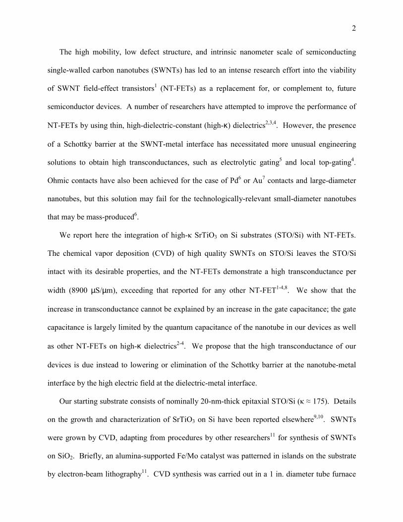
1 High-Performance Carbon Nanotube Transistors on SrTiO 3 /Si Substrates B. M. Kim a),b) , T. Brintlinger a) , E. Cobas a) , Haimei Zheng c) , and M. S. Fuhrer a),d) University of Maryland, College Park, Maryland 20742 USA Z. Yu, R. Droopad, J. Ramdani, and K. Eisenbeiser Physical Sciences Research Laboratories, Motorola Labs, Tempe, Arizona 85284 Single-walled carbon nanotubes (SWNTs) have been grown via chemical vapor deposition on high-κ dielectric SrTiO 3 /Si substrates, and high-performance semiconducting SWNT field-effect transistors have been fabricated using the thin SrTiO 3 as gate dielectric and Si as gate electrode. The transconductance per channel width is 8900 µS/µm. The high transconductance cannot be explained by the increased gate capacitance; it is proposed that the increased electric field at the nanotube-electrode interface due to the high-κ SrTiO 3 decreases or eliminates the nanotube- electrode Schottky barrier. a) Department of Physics and Center for Superconductivity Research b) Present address: Department of Mechanical Engineering and Applied Mechanics, University of Pennsylvania, Philadelphia, PA 19104 c) Department of Materials Science and Engineering, d) Electronic mail: [email protected]

Welcome message from author
This document is posted to help you gain knowledge. Please leave a comment to let me know what you think about it! Share it to your friends and learn new things together.
Transcript
1
High-Performance Carbon Nanotube Transistors on SrTiO3/Si
Substrates
B. M. Kima),b), T. Brintlingera), E. Cobasa), Haimei Zhengc), and M. S. Fuhrera),d)
University of Maryland, College Park, Maryland 20742 USA
Z. Yu, R. Droopad, J. Ramdani, and K. Eisenbeiser
Physical Sciences Research Laboratories, Motorola Labs, Tempe, Arizona 85284
Single-walled carbon nanotubes (SWNTs) have been grown via chemical vapor deposition on
high-κ dielectric SrTiO3/Si substrates, and high-performance semiconducting SWNT field-effect
transistors have been fabricated using the thin SrTiO3 as gate dielectric and Si as gate electrode.
The transconductance per channel width is 8900 µS/µm. The high transconductance cannot be
explained by the increased gate capacitance; it is proposed that the increased electric field at the
nanotube-electrode interface due to the high-κ SrTiO3 decreases or eliminates the nanotube-
electrode Schottky barrier.
a)Department of Physics and Center for Superconductivity Research
b)Present address: Department of Mechanical Engineering and Applied Mechanics,
University of Pennsylvania, Philadelphia, PA 19104
c)Department of Materials Science and Engineering,
d)Electronic mail: [email protected]
2
The high mobility, low defect structure, and intrinsic nanometer scale of semiconducting
single-walled carbon nanotubes (SWNTs) has led to an intense research effort into the viability
of SWNT field-effect transistors1 (NT-FETs) as a replacement for, or complement to, future
semiconductor devices. A number of researchers have attempted to improve the performance of
NT-FETs by using thin, high-dielectric-constant (high-κ) dielectrics2,3,4. However, the presence
of a Schottky barrier at the SWNT-metal interface has necessitated more unusual engineering
solutions to obtain high transconductances, such as electrolytic gating5 and local top-gating4.
Ohmic contacts have also been achieved for the case of Pd6 or Au7 contacts and large-diameter
nanotubes, but this solution may fail for the technologically-relevant small-diameter nanotubes
that may be mass-produced6.
We report here the integration of high-κ SrTiO3 on Si substrates (STO/Si) with NT-FETs.
The chemical vapor deposition (CVD) of high quality SWNTs on STO/Si leaves the STO/Si
intact with its desirable properties, and the NT-FETs demonstrate a high transconductance per
width (8900 µS/µm), exceeding that reported for any other NT-FET1-4,8. We show that the
increase in transconductance cannot be explained by an increase in the gate capacitance; the gate
capacitance is largely limited by the quantum capacitance of the nanotube in our devices as well
as other NT-FETs on high-κ dielectrics2-4. We propose that the high transconductance of our
devices is due instead to lowering or elimination of the Schottky barrier at the nanotube-metal
interface by the high electric field at the dielectric-metal interface.
Our starting substrate consists of nominally 20-nm-thick epitaxial STO/Si (κ ≈ 175). Details
on the growth and characterization of SrTiO3 on Si have been reported elsewhere9,10. SWNTs
were grown by CVD, adapting from procedures by other researchers11 for synthesis of SWNTs
on SiO2. Briefly, an alumina-supported Fe/Mo catalyst was patterned in islands on the substrate
by electron-beam lithography11. CVD synthesis was carried out in a 1 in. diameter tube furnace
Michael Fuhrer
3
for 11 min at 900 ºC using a methane flow of ~1900 ml/min and a hydrogen co-flow of ~480
ml/min. To ensure the STO/Si remained intact after growth, we performed transmission electron
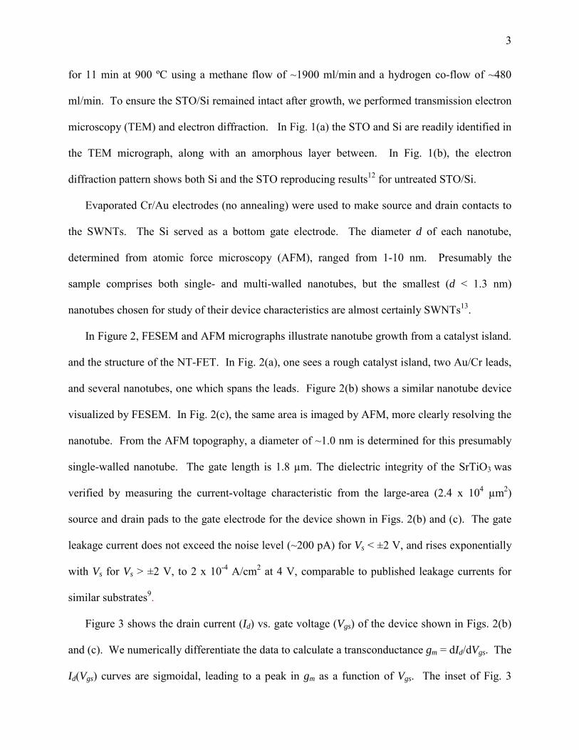
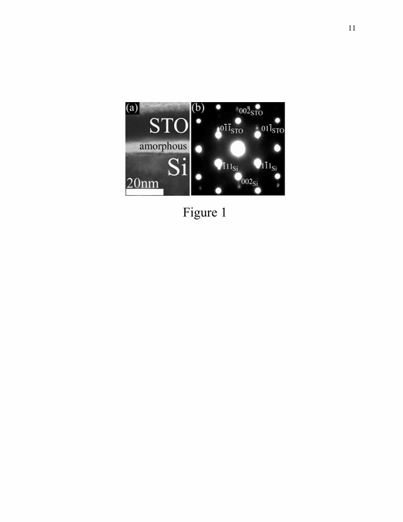
microscopy (TEM) and electron diffraction. In Fig. 1(a) the STO and Si are readily identified in
the TEM micrograph, along with an amorphous layer between. In Fig. 1(b), the electron
diffraction pattern shows both Si and the STO reproducing results12 for untreated STO/Si.
Evaporated Cr/Au electrodes (no annealing) were used to make source and drain contacts to
the SWNTs. The Si served as a bottom gate electrode. The diameter d of each nanotube,
determined from atomic force microscopy (AFM), ranged from 1-10 nm. Presumably the
sample comprises both single- and multi-walled nanotubes, but the smallest (d < 1.3 nm)
nanotubes chosen for study of their device characteristics are almost certainly SWNTs13.
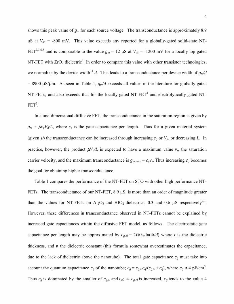
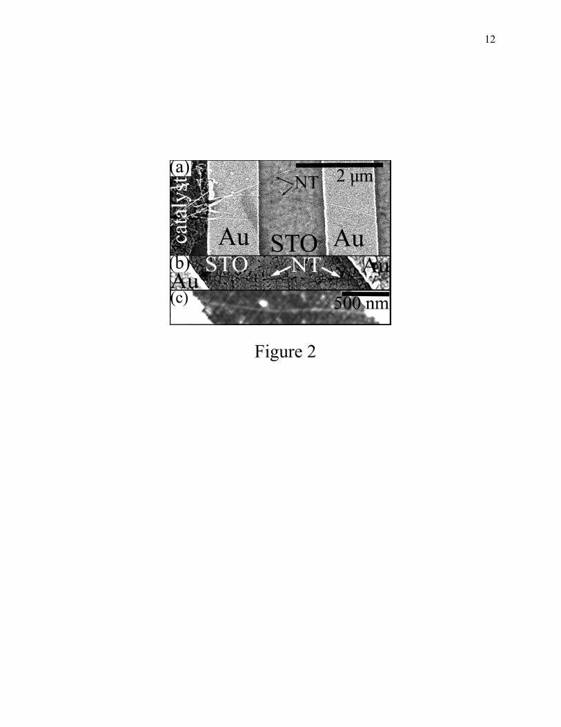
In Figure 2, FESEM and AFM micrographs illustrate nanotube growth from a catalyst island.
and the structure of the NT-FET. In Fig. 2(a), one sees a rough catalyst island, two Au/Cr leads,
and several nanotubes, one which spans the leads. Figure 2(b) shows a similar nanotube device
visualized by FESEM. In Fig. 2(c), the same area is imaged by AFM, more clearly resolving the
nanotube. From the AFM topography, a diameter of ~1.0 nm is determined for this presumably
single-walled nanotube. The gate length is 1.8 µm. The dielectric integrity of the SrTiO3 was
verified by measuring the current-voltage characteristic from the large-area (2.4 x 104 µm2)
source and drain pads to the gate electrode for the device shown in Figs. 2(b) and (c). The gate
leakage current does not exceed the noise level (~200 pA) for Vs < ±2 V, and rises exponentially
with Vs for Vs > ±2 V, to 2 x 10⁻⁴ A/cm2 at 4 V, comparable to published leakage currents for
similar substrates9.
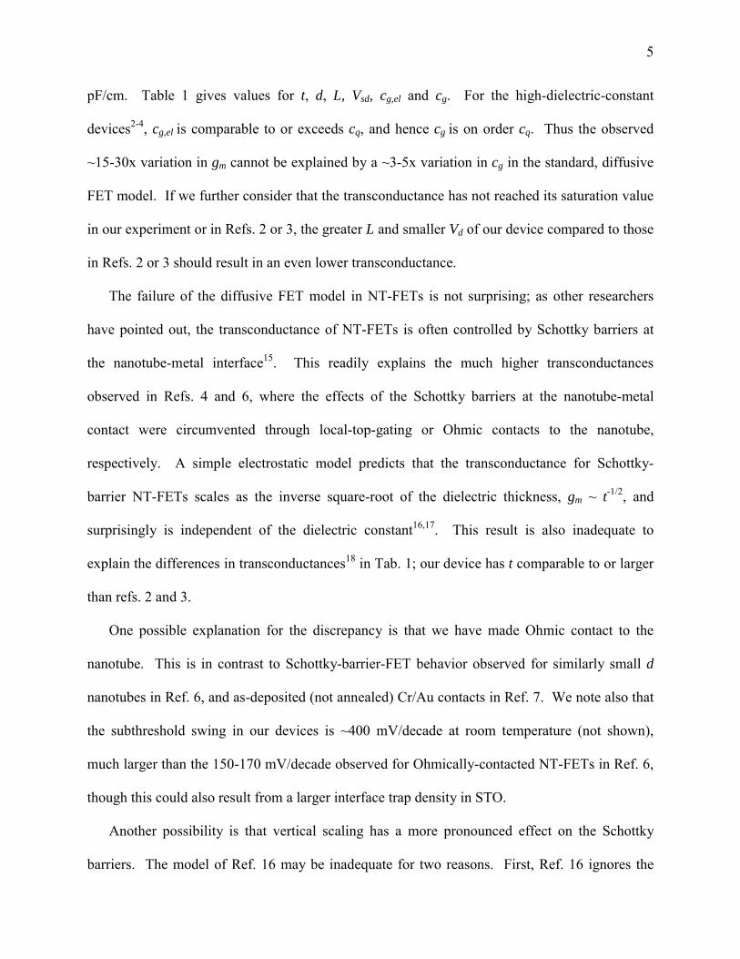
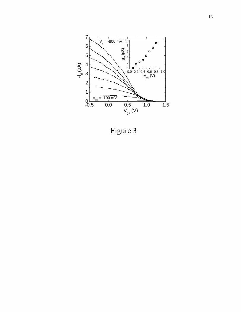
Figure 3 shows the drain current (Id) vs. gate voltage (Vgs) of the device shown in Figs. 2(b)
and (c). We numerically differentiate the data to calculate a transconductance gm = dId/dVgs. The
Id(Vgs) curves are sigmoidal, leading to a peak in gm as a function of Vgs. The inset of Fig. 3
4
shows this peak value of gm for each source voltage. The transconductance is approximately 8.9
µS at Vds = -800 mV. This value exceeds any reported for a globally-gated solid-state NT-
FET2,3,6,8 and is comparable to the value gm = 12 µS at Vds = -1200 mV for a locally-top-gated
NT-FET with ZrO2 dielectric4. In order to compare this value with other transistor technologies,
we normalize by the device width14 d. This leads to a transconductance per device width of gm/d
= 8900 µS/µm. As seen in Table 1, gm/d exceeds all values in the literature for globally-gated
NT-FETs, and also exceeds that for the locally-gated NT-FET4 and electrolytically-gated NT-
FET5.
In a one-dimensional diffusive FET, the transconductance in the saturation region is given by
gm ≈ µcgVd/L, where cg is the gate capacitance per length. Thus for a given material system
(given µ) the transconductance can be increased through increasing cg or Vd, or decreasing L. In
practice, however, the product µVd/L is expected to have a maximum value vs, the saturation
carrier velocity, and the maximum transconductance is gm,max = cgvs. Thus increasing cg becomes
the goal for obtaining higher transconductance.
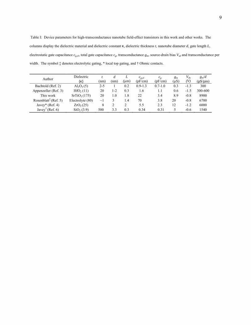
Table 1 compares the performance of the NT-FET on STO with other high performance NT-
FETs. The transconductance of our NT-FET, 8.9 µS, is more than an order of magnitude greater
than the values for NT-FETs on Al2O3 and HfO2 dielectrics, 0.3 and 0.6 µS respectively2,3.
However, these differences in transconductance observed in NT-FETs cannot be explained by
increased gate capacitances within the diffusive FET model, as follows. The electrostatic gate
capacitance per length may be approximated by cg,el = 2πκεo/ln(4t/d) where t is the dielectric
thickness, and κ the dielectric constant (this formula somewhat overestimates the capacitance,
due to the lack of dielectric above the nanotube). The total gate capacitance cg must take into
account the quantum capacitance cq of the nanotube; cg = cg,elcq/(cg,el + cq), where cq ≈ 4 pF/cm5.
Thus cg is dominated by the smaller of cg,el and cq; as cg,el is increased, cg tends to the value 4
5
pF/cm. Table 1 gives values for t, d, L, Vsd, cg,el and cg. For the high-dielectric-constant
devices2-4, cg,el is comparable to or exceeds cq, and hence cg is on order cq. Thus the observed
~15-30x variation in gm cannot be explained by a ~3-5x variation in cg in the standard, diffusive
FET model. If we further consider that the transconductance has not reached its saturation value
in our experiment or in Refs. 2 or 3, the greater L and smaller Vd of our device compared to those
in Refs. 2 or 3 should result in an even lower transconductance.
The failure of the diffusive FET model in NT-FETs is not surprising; as other researchers
have pointed out, the transconductance of NT-FETs is often controlled by Schottky barriers at
the nanotube-metal interface15. This readily explains the much higher transconductances
observed in Refs. 4 and 6, where the effects of the Schottky barriers at the nanotube-metal
contact were circumvented through local-top-gating or Ohmic contacts to the nanotube,
respectively. A simple electrostatic model predicts that the transconductance for Schottky-
barrier NT-FETs scales as the inverse square-root of the dielectric thickness, gm ~ t-1/2, and
surprisingly is independent of the dielectric constant16,17. This result is also inadequate to
explain the differences in transconductances18 in Tab. 1; our device has t comparable to or larger
than refs. 2 and 3.
One possible explanation for the discrepancy is that we have made Ohmic contact to the
nanotube. This is in contrast to Schottky-barrier-FET behavior observed for similarly small d
nanotubes in Ref. 6, and as-deposited (not annealed) Cr/Au contacts in Ref. 7. We note also that
the subthreshold swing in our devices is ~400 mV/decade at room temperature (not shown),
much larger than the 150-170 mV/decade observed for Ohmically-contacted NT-FETs in Ref. 6,
though this could also result from a larger interface trap density in STO.
Another possibility is that vertical scaling has a more pronounced effect on the Schottky
barriers. The model of Ref. 16 may be inadequate for two reasons. First, Ref. 16 ignores the
6
charge in the nanotube channel. A self-consistent treatment of charge in the on-state does show
increases in device on-current for increased dielectric constants19. Second, Ref. 16 treats the
nanotube as infinitely thin. We expect that the details of the electric field at the contacts will be
substantially modified when the effective thickness of the dielectric t’ = t/κ becomes
significantly less than the nanotube diameter d (the dielectric constant of the nanotube is unity20).
In our devices, t’/d ≈ 0.1, significantly less than the values of t’/d ≈ 0.2-0.6 and 1-2 in refs. 2 and
3 respectively. (For typical devices fabricated on thick SiO2, t’/d ≈ 100.) When t’/d << 1, the
potential drop across the nanotube diameter for the portion of nanotube underneath the electrode
becomes a large fraction of the applied gate voltage. When the voltage drop across the radius of
the nanotube is equal to the Schottky barrier height, population of the valence band with carriers
should become energetically favorable, allowing Ohmic contact with the channel. Stated another
way, at moderate gate voltages the shift in electrostatic potential of the nanotube relative to the
metal electrode can be greater than the Schottky barrier height, eliminating the barrier. In our
devices this would occur at an applied gate voltage of a few hundred mV from threshold. This
model offers an alternate explanation for the observation of high transconductances (even in
small diameter nanotubes) in FETs with an electrolyte dielectric5 (t’/d ≈ 0.01).
Acknowledgements:
This research was supported by ARDA and the Office of Naval Research through grant
N000140110995, the Director of Central Intelligence Postdoctoral Research Fellowship
Program, and the National Science Foundation through grant DMR-0102950. The authors are
grateful for helpful conversations with Frank D. Gac and Ramamoorthy Ramesh.
7
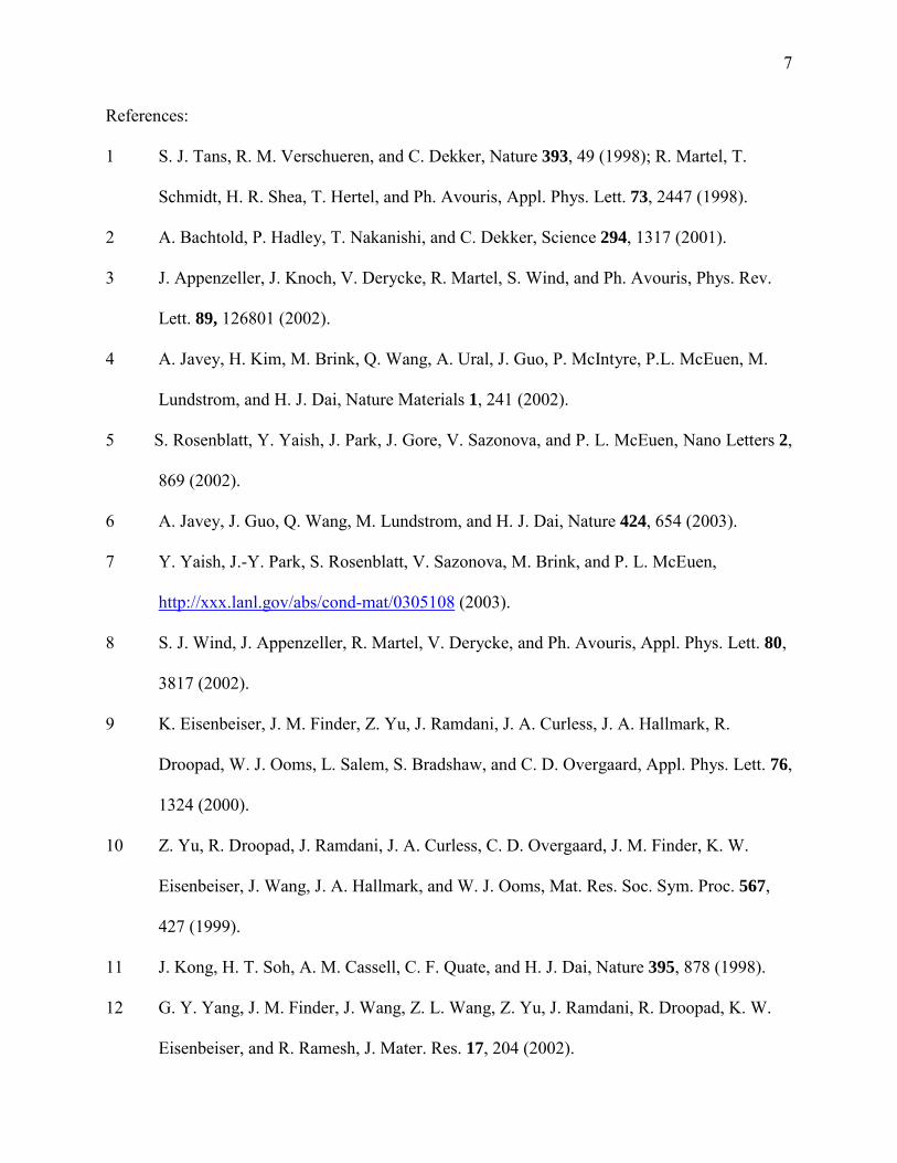
References:
1 S. J. Tans, R. M. Verschueren, and C. Dekker, Nature 393, 49 (1998); R. Martel, T.
Schmidt, H. R. Shea, T. Hertel, and Ph. Avouris, Appl. Phys. Lett. 73, 2447 (1998).
2 A. Bachtold, P. Hadley, T. Nakanishi, and C. Dekker, Science 294, 1317 (2001).
3 J. Appenzeller, J. Knoch, V. Derycke, R. Martel, S. Wind, and Ph. Avouris, Phys. Rev.
Lett. 89, 126801 (2002).
4 A. Javey, H. Kim, M. Brink, Q. Wang, A. Ural, J. Guo, P. McIntyre, P.L. McEuen, M.
Lundstrom, and H. J. Dai, Nature Materials 1, 241 (2002).
5 S. Rosenblatt, Y. Yaish, J. Park, J. Gore, V. Sazonova, and P. L. McEuen, Nano Letters 2,
869 (2002).
6 A. Javey, J. Guo, Q. Wang, M. Lundstrom, and H. J. Dai, Nature 424, 654 (2003).
7 Y. Yaish, J.-Y. Park, S. Rosenblatt, V. Sazonova, M. Brink, and P. L. McEuen,
http://xxx.lanl.gov/abs/cond-mat/0305108 (2003).
8 S. J. Wind, J. Appenzeller, R. Martel, V. Derycke, and Ph. Avouris, Appl. Phys. Lett. 80,
3817 (2002).
9 K. Eisenbeiser, J. M. Finder, Z. Yu, J. Ramdani, J. A. Curless, J. A. Hallmark, R.
Droopad, W. J. Ooms, L. Salem, S. Bradshaw, and C. D. Overgaard, Appl. Phys. Lett. 76,
1324 (2000).
10 Z. Yu, R. Droopad, J. Ramdani, J. A. Curless, C. D. Overgaard, J. M. Finder, K. W.
Eisenbeiser, J. Wang, J. A. Hallmark, and W. J. Ooms, Mat. Res. Soc. Sym. Proc. 567,
427 (1999).
11 J. Kong, H. T. Soh, A. M. Cassell, C. F. Quate, and H. J. Dai, Nature 395, 878 (1998).
12 G. Y. Yang, J. M. Finder, J. Wang, Z. L. Wang, Z. Yu, J. Ramdani, R. Droopad, K. W.
Eisenbeiser, and R. Ramesh, J. Mater. Res. 17, 204 (2002).
8
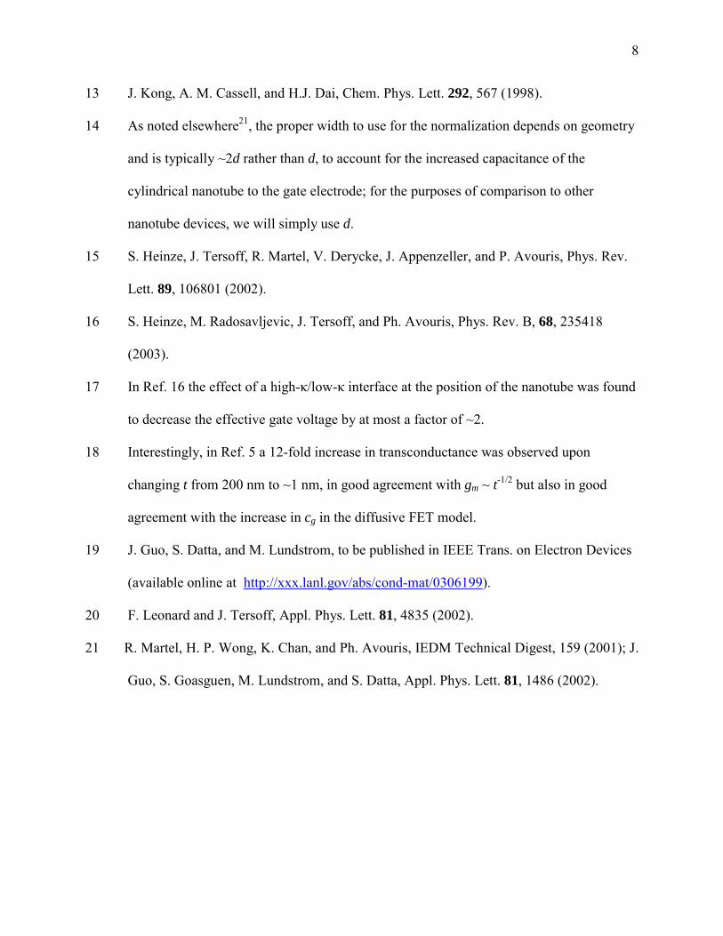
13 J. Kong, A. M. Cassell, and H.J. Dai, Chem. Phys. Lett. 292, 567 (1998).
14 As noted elsewhere21, the proper width to use for the normalization depends on geometry
and is typically ~2d rather than d, to account for the increased capacitance of the
cylindrical nanotube to the gate electrode; for the purposes of comparison to other
nanotube devices, we will simply use d.
15 S. Heinze, J. Tersoff, R. Martel, V. Derycke, J. Appenzeller, and P. Avouris, Phys. Rev.
Lett. 89, 106801 (2002).
16 S. Heinze, M. Radosavljevic, J. Tersoff, and Ph. Avouris, Phys. Rev. B, 68, 235418
(2003).
17 In Ref. 16 the effect of a high-κ/low-κ interface at the position of the nanotube was found
to decrease the effective gate voltage by at most a factor of ~2.
18 Interestingly, in Ref. 5 a 12-fold increase in transconductance was observed upon
changing t from 200 nm to ~1 nm, in good agreement with gm ~ t-1/2 but also in good
agreement with the increase in cg in the diffusive FET model.
19 J. Guo, S. Datta, and M. Lundstrom, to be published in IEEE Trans. on Electron Devices
(available online at http://xxx.lanl.gov/abs/cond-mat/0306199).
20 F. Leonard and J. Tersoff, Appl. Phys. Lett. 81, 4835 (2002).
21 R. Martel, H. P. Wong, K. Chan, and Ph. Avouris, IEDM Technical Digest, 159 (2001); J.
Guo, S. Goasguen, M. Lundstrom, and S. Datta, Appl. Phys. Lett. 81, 1486 (2002).
9
Table I: Device parameters for high-transconductance nanotube field-effect transistors in this work and other works. The
columns display the dielectric material and dielectric constant κ, dielectric thickness t, nanotube diameter d, gate length L,
electrostatic gate capacitance cg,el, total gate capacitance cg, transconductance gm, source-drain bias Vsd and transconductance per
width. The symbol � denotes electrolytic gating, * local top gating, and � Ohmic contacts.
Author Dielectric (κ)
t (nm)
d (nm)
L (µm)
cg,el
(pF/cm) cg
(pF/cm) gm
(µS) Vds (V)
gm/d (µS/µm)
Bachtold (Ref. 2) Al2O3 (5) 2-5 1 0.2 0.9-1.3 0.7-1.0 0.3 -1.3 300 Appenzeller (Ref. 3) HfO2 (11) 20 1-2 0.3 1.6 1.1 0.6 -1.5 300-600
This work SrTiO3 (175) 20 1.0 1.8 22 3.4 8.9 -0.8 8900 Rosenblatt� (Ref. 5) Electrolyte (80) ~1 3 1.4 70 3.8 20 -0.8 6700
Javey* (Ref. 4) ZrO2 (25) 8 2 2 5.5 2.3 12 -1.2 6000 Javey� (Ref. 6) SiO2 (3.9) 500 3.3 0.3 0.34 0.31 5 -0.6 1540
10
Figure Captions
Fig. 1. Transmission electron (a) micrograph and (b) diffraction pattern. In (a), the crystalline
SrTiO3, amorphous interface layer, and crystalline Si substrate are resolved in profile. In (b),
two sets of diffraction spots reveal the presence of SrTiO3 and Si.
Fig. 2. Images of carbon nanotubes grown on SrTiO3 (STO) substrates by chemical vapor
deposition. (a) showing patterned catalyst (left) on STO, as well as several nanotubes extending
from the catalyst island. One nanotube has been contacted by two Cr/Au electrodes. (b) Field-
emission scanning electron micrograph of a semiconducting nanotube on STO bridging two
Cr/Au contacts with 1.8 um separation. (c) AFM image of the nanotube in (b).
Fig. 3. Drain current (-Id) as a function of gate voltage (Vgs) at drain voltages (Vds) of -100 mV to
-800 mV in 100 mV steps, at room temperature. Inset shows the maximum transconductance
dId/dVgs calculated from these data.
11
Figure 1
12
Figure 2
13
-0.5 0.0 0.5 1.0 1.50
1
2
3
4
5
6
7
0.0 0.2 0.4 0.6 0.8 1.00
2
4
6
8
10Vs = -800 mV
Vds = -100 mV
-Vds (V)
g m (µ
S)
-I d (µA)
Vgs (V)
Figure 3
Related Documents