High-Order Modulation Signal Generator and Its DSP Implementation Yecai Guo 1, 2, a * , Lijian Cai 1, b and Xiang Wang 1, c 1 College of Electronic and information Engineering, Nanjing University of Information Science and Technology, Nanjing 210044, China 2 Collaborative Innovation Center of Atmospheric Environment and Equipment Technology, Nanjing 210044, China a [email protected], b [email protected], c [email protected] *The Corresponding author Keywords: Higher order modulation signal generator; Software radio; DSP; DDS Abstract. In recent years, the low-order modulation signal cannot meet current demands due to the band tension and high demand of data transfer rate. In this paper, a higher-order modulation signal generator based on software-defined radio idea was designed. The design implements an efficient plan based on DDS technology by combining the TMS320C5509 chip with CPLD, which can send and receive signals and do floating-point data operation by the method of a 16-bit fixed-point DSP calibration. The validity of the proposed method has been verified by CCS simulation of the 64 QAM, 128 QAM and 256 QAM signal constellation graph mapping. Introduction Modulation signal generator is the essential part of communication and communication countermeasure, and the significant one of communication system design and electromagnetic environment simulation. It is wildly used in communication, radar, measurement, and control, etc.[1]. Traditional low-order signal generator has a lot of deficiencies such as low utilization rate of spectrum, serious radiation when transmission is outside the bandwidth and poor ability of anti-interference. In the high-speed data transmission communication system, it is equally important to improve the band utilization and ensure the low symbol error rate of the system. Therefore, It is very necessary to design a DSP-based digital communication system of the high-order signal generator. So, in this paper, the high-order modulation signal generator based on based on combining DSP with CPLD was proposed to meet different demands. Overall Structure TMS320C5509DSP is used as the main control component of the circuit, which can modulate digital signal of input binary data, such as quadrature amplitude modulation (QAM).The EPM240T100C, connected with DSP external I/O, is used to control selection based on a 44 × matrix keyboard. We has designed the DDS module to generate a sinusoidal sequence, whose modulus are stored into the SDRAM and DSP reads the data to choose carrier wave. DAC900E is a 10Bit, 165MSPS high-speed D/A conversion chip, and used for signal output. We use DDS as the buffer between DSP and DAC900E [2]. Besides, the design of FLASH module, loading when starts, contributes to DSP to run offline, and the asynchronous serial port module can get real-time data for transmission and display constellation and waveform on VC. The specific block diagram is shown in Fig.1. This is an open access article under the CC BY-NC license (http://creativecommons.org/licenses/by-nc/4.0/). Copyright © 2017, the Authors. Published by Atlantis Press. 1218 Advances in Computer Science Research (ACSR), volume 76 7th International Conference on Education, Management, Information and Mechanical Engineering (EMIM 2017)

Welcome message from author
This document is posted to help you gain knowledge. Please leave a comment to let me know what you think about it! Share it to your friends and learn new things together.
Transcript
High-Order Modulation Signal Generator and Its DSP Implementation
Yecai Guo1, 2, a *, Lijian Cai1, b and Xiang Wang1, c 1College of Electronic and information Engineering, Nanjing University of Information Science and
Technology, Nanjing 210044, China
2Collaborative Innovation Center of Atmospheric Environment and Equipment Technology, Nanjing 210044, China
[email protected], [email protected], [email protected]
*The Corresponding author
Keywords: Higher order modulation signal generator; Software radio; DSP; DDS
Abstract. In recent years, the low-order modulation signal cannot meet current demands due to the
band tension and high demand of data transfer rate. In this paper, a higher-order modulation signal
generator based on software-defined radio idea was designed. The design implements an efficient
plan based on DDS technology by combining the TMS320C5509 chip with CPLD, which can send
and receive signals and do floating-point data operation by the method of a 16-bit fixed-point DSP
calibration. The validity of the proposed method has been verified by CCS simulation of the 64
QAM, 128 QAM and 256 QAM signal constellation graph mapping.
Introduction
Modulation signal generator is the essential part of communication and communication
countermeasure, and the significant one of communication system design and electromagnetic
environment simulation. It is wildly used in communication, radar, measurement, and control,
etc.[1]. Traditional low-order signal generator has a lot of deficiencies such as low utilization rate of
spectrum, serious radiation when transmission is outside the bandwidth and poor ability of
anti-interference. In the high-speed data transmission communication system, it is equally important
to improve the band utilization and ensure the low symbol error rate of the system. Therefore, It is
very necessary to design a DSP-based digital communication system of the high-order signal
generator.
So, in this paper, the high-order modulation signal generator based on based on combining DSP
with CPLD was proposed to meet different demands.
Overall Structure
TMS320C5509DSP is used as the main control component of the circuit, which can modulate
digital signal of input binary data, such as quadrature amplitude modulation (QAM).The
EPM240T100C, connected with DSP external I/O, is used to control selection based on a 4 4×
matrix keyboard. We has designed the DDS module to generate a sinusoidal sequence, whose
modulus are stored into the SDRAM and DSP reads the data to choose carrier wave. DAC900E is a
10Bit, 165MSPS high-speed D/A conversion chip, and used for signal output. We use DDS as the
buffer between DSP and DAC900E [2]. Besides, the design of FLASH module, loading when starts,
contributes to DSP to run offline, and the asynchronous serial port module can get real-time data for
transmission and display constellation and waveform on VC. The specific block diagram is shown
in Fig.1.
This is an open access article under the CC BY-NC license (http://creativecommons.org/licenses/by-nc/4.0/).
Copyright © 2017, the Authors. Published by Atlantis Press. 1218
Advances in Computer Science Research (ACSR), volume 767th International Conference on Education, Management, Information and Mechanical Engineering (EMIM 2017)

16QAM 64QAM 128QAM
16PSK 64PSK 256QAM
Serial port
modeReset
Sinusoidal
signal
Figure 1. Finite Finite Hardware specific block diagram
Hardware Design
Signal Processing Module Design. TMS320VC5509 (hereinafter referred to as VC5509) from TI
company is used as DSP chip. EMP240T100C5 of Altera MAX II series as the controller and
HY57641620 of 4M memory used for SDRAM as a synchronous memory chip to extend the
external DSP space are implemented in this system. DSP external input clock is 10MHZ, and its
working clock is 144MHZ through the internal PLL multiplier. DSP is supplied by dual power,
whose standard voltage is 1.8V and I/O voltage is 3.3V. Its low 10-bit address line and 16-bit data
line are connected to CPLD. External module is connected with CPLD by decoding module and the
controlling signal is produced by XF of DSP I/O port which is also connected with CPLD. Bit
synchronizing signal and digital baseband signals are input via the DSP external interrupt pins INT0
and GPIO0, respectively. At this time, DSP can select the corresponding digital modulation
algorithm for data processing according to the key. After that, DSP places the data into the SDRAM
and if XF=0, we can be informed that the CPLD has completed the digital modulation process.
Finally, CPLD reads the signal that has been modulated by SDRAM and sends it to the DAC
converter for external output.
FLASH Memory Interface Technology. Since we generally use the VC5509 of LQFP
package, it has only 14-bit address line pin, and can only address the range of 8K×16bit space. But if we want to address the AM29LV800 512K×16 bit memory, 19 address line are needed.
The solution is that we can use the programmable logic device CPLD for logic decoding, that is,
we control the outputs through different inputs to complete different functions. The VC5509
EMIF asynchronous interface AWE and ARE are connected with 16-bit wide FLASH OE and
WE pin to control external memory for reading and writing. The low address A [0:12] of FLASH
is provided by A [1:13] of VC5509 and the high address FA [13:18] is provided by CPLD. The
other 16 data buses are directly connected. CPLD is connected to the low 8-bit address pins and
16-bit data pins of the VC5509 for communication and as a decoder to expand the external I / O
port. The byte select pin and the reset pin of the FLASH device are connected to CPLD and
controlled by CPLD.
The reading and writting process of the FLASH is given as follows. DSP clock and CPU
initialization is the first step, and then we program the FLASH into the working state and set the
EMIF global control register and CE1 related control register. According to the function of
AM29LV800B, we can erase the entire chip memory. In the bootloader mode, VC5509 writes
data to the address of 0x400000 to 0x800000 and the 0xFFFF of Flash must be stored the first
address of the boot table. Afterwards, under the control of CCS3.3, the Boot table is written to
FLASH. Finally, the contents written into FLASH are read out to check in which VC5509 would
automatically implement when it has been powered.
1219
Advances in Computer Science Research (ACSR), volume 76

Software Design
DDS implementation. A direct digital frequency synthesizer consists of phase accumulator, adder,
waveform ROM, D/A converter and low pass filter (LPF) structure. The reference oscillator
provides a stable time base for the system and determines the frequency accuracy of the DDS. It
provides the clock to the NCO which produces a discrete-time and quantized version of the desired
waveform at its output(often a sinusoid) whose period is controlled by the digital word contained in
the Frequency Control Register. The digital waveform is converted to an analog waveform by the
DAC. The output reconstruction filter rejects the spectral replicas produced by the zero-order hold
inherent in the analog conversion process[3][4].
In the paper, the determination of the frequency, amplitude, carrier source whose phase is
adjustable, are the foundation and key of the design of the high-order modulation signal generator.
In VC5509 system, each time the implementation of a timer interrupt program would output a data
point. The timer interval is 50 DSP clocks, so the DDS system clock is 2MHz .The low 30 bits of
accumulator in designed program are used as accumulator registers. As the DDS system
clocks 2MHzf = , according to the DDS principle, we can determine some data such as the system
frequency resolution 30∆f=2MHz/2 =0.00186Hz , output frequency f m 0.00186Hz= × , theoretical
output maximum frequency is 1MHz and actual maximum output frequency is 40% of the system
clock, that is800KHz . To complete the waveform reconstruction, DDS algorithm sample the sine
discrete table fixed in the FLASH under cetain frequency. In order to improve the speed, we usually
place the initialization of the discrete sine table to the internal high-speed RAM to run.
Quadrature Amplitude Modulation (QAM) Theory. Quadrature amplitude modulation (QAM)
is a kind of modulation method with high spectrum utilization. Compared with other modulation
methods, it has a higher data transmission rate, and it is very competitive in the future
communication field. In order to adapt to the changing wireless channel, high-order modulation
signal can greatly improve the efficiency of data transmission.
QAM is a vector modulation. First, the input bit (usually the Gray code) maps to a complex
plane (constellation), In which the bit can be transformed into complex modulation symbols. Then
the I and Q component of the symbol (corresponding to the real and imagine part, that is the
horizontal and vertical one of the complex plane) are taken with amplitude modulation, which,
respectively, correspond to the two carrier( ccos tω and csin tω generated by the DDS) [5]. Therefore,
it will exponentially increase the spectrum utilization compared to amplitude modulation (AM).
QAM is a Joint tachnique of magnitude and phase , which utilizes the amplitude and phase of the
carrier to transmit the information bits, so that higher band utilization can be achieved with specific
and identical conditions[5]. Ideally, if carrier states of the M-QAM is M, it can modulate 2log M bits.
The signal form of M-QAM is given as
(1)
where mcA and msA are the quadrature carrier carrying information, ( )g t is the baseband waveform
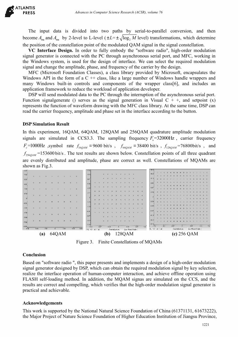
pulse after forming. QAM signal modulation principle is shown in Fig.2.
Figure 2. Finite QAM modulation principle diagram
( ) 2
m e mc ms( ) R ( ) cj f ts t A jA g t e
π = + mc c ms c( )cos(2 ) ( )sin(2 ) ( 1,2, M,0 T)A g t f t A g t f t m tπ π= − = ≤ ≤…
1220
Advances in Computer Science Research (ACSR), volume 76
The input data is divided into two paths by serial-to-parallel conversion, and then
become mcA and msA by 2-level to L-level ( 2= logL M± ± level) transformations, which determine
the position of the constellation point of the modulated QAM signal in the signal constellation.
VC Interface Design. In order to fully embody the "software radio", high-order modulation
signal generator is connected with the PC through asynchronous serial port, and MFC, working in
the Windows system, is used for the design of interface. We can select the required modulation
signal and change the amplitude, phase, and frequency of the carrier by the design.
MFC (Microsoft Foundation Classes), a class library provided by Microsoft, encapsulates the
Windows API in the form of a C ++ class, like a large number of Windows handle wrappers and
many Windows built-in controls and components of the wrapper class[6], and includes an
application framework to reduce the workload of application developer.
DSP will send modulated data to the PC through the interruption of the asynchronous serial port.
Function signalgenerate () serves as the signal generation in Visual C + +, and setpoint (x)
represents the function of waveform drawing with the MFC class library. At the same time, DSP can
read the carrier frequency, amplitude and phase set in the interface according to the button.
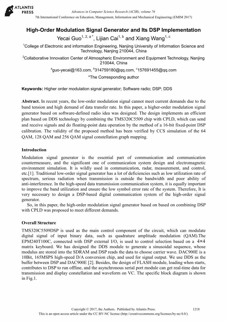
DSP Simulation Result
In this experiment, 16QAM, 64QAM, 128QAM and 256QAM quadrature amplitude modulation
signals are simulated in CCS3.3. The sampling frequency s=32000HzF , carrier frequency
=1000HzcF ,symbol rate16 9600 bit/sQAMf = ,
64 38400 bit/sQAMf = ,128 76800bi /s= tQAMf , and
256QAMf =153600 bit/s . The test results are shown below. Constellation points of all three quadrant
are evenly distributed and amplitude, phase are correct as well. Constellations of MQAMs are
shown as Fig.3.
(a) 64QAM (b) 128QAM (c) 256 QAM
Figure 3. Finite Constellations of MQAMs
Conclusion
Based on "software radio ", this paper presents and implements a design of a high-order modulation
signal generator designed by DSP, which can obtain the required modulation signal by key selection,
realize the interface operation of human-computer interaction, and achieve offline operation using
FLASH self-loading method. In addition, the MQAM signas are simulated on the CCS, and the
results are correct and compelling, which verifies that the high-order modulation signal generator is
practical and achievable.
Acknowledgements
This work is supported by the National Natural Science Foundation of China (61371131, 61673222),
the Major Project of Nature Science Foundation of Higher Education Institution of Jiangsu Province,
1221
Advances in Computer Science Research (ACSR), volume 76

China(Grant No.13KJA510001), Jiangsu Scientific Research Achievements in Industrialization
Project, China(JHB 2012-9), Jiangsu Province, and Top- notch Academic Programs Project of
Jiangsu Higher Education Institutions(TAPP, PPZY 2015 B134).
References
[1] Lin Chongfeng, Ling longxue, Suo Yun. Design of multi-function and high precision signal
generator based on DDS, Electronic Science and Technology, 26 (2013)127-130.
[2] Yang Dongxia, Ju Yongfeng. Design and implementation of digital modulation signal generator
based on FPGA and DDS, Electronic Design Engineering, 21 (2013) 90-93.
[3] Zhao Xiaoyan, DSP modulation algorithm based on DDS principle and its realization, Journal of
Chongqing University of Science and Technology, 12 (2012) 135-140.
[4] Zhang Fangzheng, Research on digital signal processing (DSP) and wave generation in high
speed optical communication [D]. Beijing University of Posts and Telecommunications, 2013,
27-50.
[5] Li Xiaolin, Liu Wenwen.64QAM modulation implement based on DSP, Journal of Chongqing
University of Science and Technology, 38 (2012,): 43-45.
[6] Li Jiujin, From MFC Design to MFC Programming, first ed, Huazhong University of science
and Technology Press, 2006.
1222
Advances in Computer Science Research (ACSR), volume 76
Related Documents


