[AK4118A] MS1130-E-03 2013/09 - 1 - GENERAL DESCRIPTION The AK4118A is a digital audio transceiver supporting 192kHz, 24bits. The channel status decoder supports both consumer and professional modes. The AK4118A can automatically detect a Non-PCM bit stream. When combined with the multi channel codec (AK4626A or AK4628A), the two chips provide a system solution for AC-3 applications. The dedicated pins or a serial μP I/F can control the mode setting. The small package, 48pin LQFP saves the system space. *AC-3 is a trademark of Dolby Laboratories. FEATURES AES3, IEC60958, S/PDIF, EIAJ CP1201 Compatible Low jitter Analog PLL PLL Lock Range: 8kHz 192kHz Clock Source: PLL or X'tal 8-channel Receiver input 2-channel Transmission output (Through output or DIT) Auxiliary digital input De-emphasis for 32kHz, 44.1kHz, 48kHz and 96kHz Detection Functions Non-PCM Bit Stream Detection DTS-CD Bit Stream Detection Sampling Frequency Detection (32kHz, 44.1kHz, 48kHz, 88.2kHz, 96kHz, 176.4kHz, 192kHz) Unlock & Parity Error Detection Validity Flag Detection DAT Start ID Detection Up to 24bit Audio Data Format Audio I/F: Master or Slave Mode 42-bit Channel Status Buffer Burst Preamble bit Pc and Pd Buffer for Non-PCM bit stream Q-subcode Buffer for CD bit stream Serial μP I/F (I 2 C, SPI) Two Master Clock Outputs: 64fs/128fs/256fs/512fs Operating Voltage: 2.7 to 3.6V with 5V tolerance 8GPIO Port RX Data Input Detection Small Package: 48pin LQFP Ta: -10 to 70C High Feature 192kHz 24bit Digital Audio I/F Transceiver AK4118A

Welcome message from author
This document is posted to help you gain knowledge. Please leave a comment to let me know what you think about it! Share it to your friends and learn new things together.
Transcript

[AK4118A]
MS1130-E-03 2013/09
- 1 -
GENERAL DESCRIPTION
The AK4118A is a digital audio transceiver supporting 192kHz, 24bits. The channel status decoder
supports both consumer and professional modes. The AK4118A can automatically detect a Non-PCM
bit stream. When combined with the multi channel codec (AK4626A or AK4628A), the two chips provide
a system solution for AC3 applications. The dedicated pins or a serial µP I/F can control the mode
setting. The small package, 48pin LQFP saves the system space.
*AC3 is a trademark of Dolby Laboratories.
FEATURES
AES3, IEC60958, S/PDIF, EIAJ CP1201 Compatible
Low jitter Analog PLL
PLL Lock Range: 8kHz 192kHz
Clock Source: PLL or X'tal
8-channel Receiver input
2-channel Transmission output (Through output or DIT)
Auxiliary digital input
Deemphasis for 32kHz, 44.1kHz, 48kHz and 96kHz
Detection Functions
Non-PCM Bit Stream Detection
DTS-CD Bit Stream Detection
Sampling Frequency Detection
(32kHz, 44.1kHz, 48kHz, 88.2kHz, 96kHz, 176.4kHz, 192kHz)
Unlock & Parity Error Detection
Validity Flag Detection
DAT Start ID Detection
Up to 24bit Audio Data Format
Audio I/F: Master or Slave Mode
42-bit Channel Status Buffer
Burst Preamble bit Pc and Pd Buffer for Non-PCM bit stream
Q-subcode Buffer for CD bit stream
Serial µP I/F (I2C, SPI)
Two Master Clock Outputs: 64fs/128fs/256fs/512fs
Operating Voltage: 2.7 to 3.6V with 5V tolerance
8GPIO Port
RX Data Input Detection
Small Package: 48pin LQFP
Ta: 10 to 70C
High Feature 192kHz 24bit Digital Audio I/F Transceiver
AK4118A

[AK4118A]
MS1130-E-03 2013/09
- 2 -
■ Block Diagram
Input
Selector
Clock
Recovery Clock
Generator
DAIF
Decoder
AC-3/MPEG
Detect
DEM
µP I/F
Audio
I/F
X'tal
Oscillator
PDN
INT0 P/S=”L”
LRCK
BICK
SDTO
DAUX
MCKO2
XTO XTI R AVDD AVSS
CDTI
CDTO
CCLK
CSN DVDD
DVSS
TVDD
MCKO1
IIC
RX0
RX1
RX2
RX3
RX4
RX5
RX6
RX7
DIT
TX0
Error &
Detect
STATUS
INT1
Q-subcode
buffer
TX1
B,C,U,VOUT
8 to 3
VIN GP0,1,2,3,4,5,6,7
Serial Control Mode
Input Selector
Clock
Recovery Clock
Generator
DAIF
Decoder
AC-3/MPEG
Detect
DEM
Audio
I/F
X'tal
Oscillator
PDN
INT0 P/S=”H”
LRCK
BICK
SDTO
DAUX
XTO XTI R AVDD AVSS
CM1
CM0
OCKS1
OCKS0
DVDD
DVSS
TVDD
IPS1
RX0
RX1
RX2
RX3
IPS0
DIF0
DIF1
DIF2
DIT
TX0
Error &
Detect
STATUS
INT1
TX1
B,C,U,VOUT
4 to 2
VIN
MCKO2
MCKO1
Parallel Control Mode

[AK4118A]
MS1130-E-03 2013/09
- 3 -
■ Ordering Guide
AK4118AEQ 10 ~ +70 C 48pin LQFP (0.5mm pitch)
AKD4118A Evaluation Board for AK4118A
■ Pin Layout
INT1
INT
0
37
AVDD
36
38
R 39
VCOM 40
VSS3 41
RX0 42
NC 43
RX1 44
TEST1 45
RX2 46
VSS4
OC
KS
0/C
SN
/CA
D0
35
OC
KS
1/C
CLK
/SC
L
34
33
32
PD
N
31
XT
I 30
XT
O
29
DA
UX
28
MC
KO
2
27
BIC
K
26
IPS
0/R
X4
1
NC
2
DIF
0/R
X5
3
TE
ST
2
4
DIF
1/R
X6
5
6
DIF
2/R
X7
7
IPS
1/IIC
8
PS
N
9
XT
L0
10
XT
L1
11
24
23
22
21
20
19
18
17
16
15
14
LRCK
MCKO1
VSS2
DVDD
VOUT/GP7
UOUT/GP6
COUT/GP5
BOUT/GP4
TX1/GP3
TX0/GP2
GP1
AK4118AEQ
Top View
VS
S1
CM
1/C
DT
I/S
DA
CM
0/C
DT
O/C
AD
1
SD
TO
25
VIN
/GP
0
12
47
RX3 48 13 TVDD
[AK4118A]
MS1130-E-03 2013/09
- 4 -
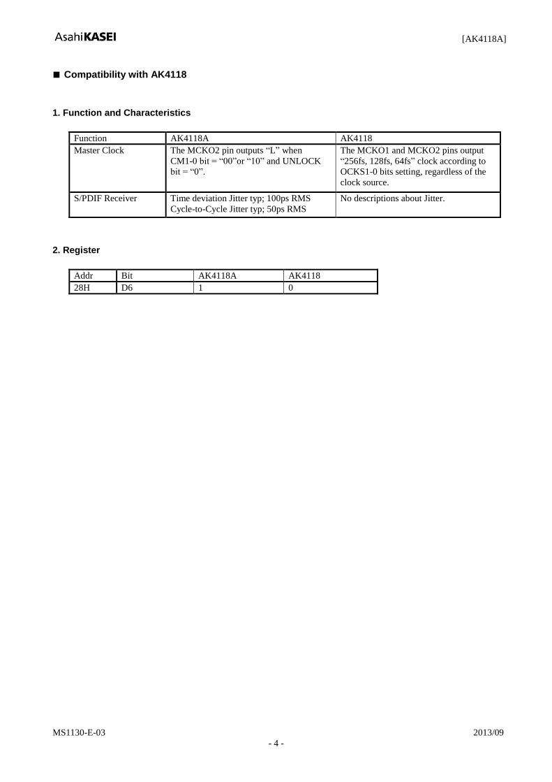
■ Compatibility with AK4118
1. Function and Characteristics
Function AK4118A AK4118
Master Clock The MCKO2 pin outputs “L” when
CM1-0 bit = “00”or “10” and UNLOCK
bit = “0”.
The MCKO1 and MCKO2 pins output
“256fs, 128fs, 64fs” clock according to
OCKS1-0 bits setting, regardless of the
clock source.
S/PDIF Receiver Time deviation Jitter typ; 100ps RMS
Cycle-to-Cycle Jitter typ; 50ps RMS
No descriptions about Jitter.
2. Register
Addr Bit AK4118A AK4118
28H D6 1 0

[AK4118A]
MS1130-E-03 2013/09
- 5 -
PIN/FUNCTION
No. Pin Name I/O Function
1 IPS0 I Input Channel Select 0 Pin in Parallel Mode
RX4 I Receiver Channel 4 Pin in Serial Mode (Internal biased pin)
2 NC I No Connect
No internal bonding. This pin should be connected to VSS3.
3 DIF0 I Audio Data Interface Format 0 Pin in Parallel Mode
RX5 I Receiver Channel 5 Pin in Serial Mode (Internal biased pin)
4 TEST2 I TEST 2 pin
This pin should be connect to VSS3.
5 DIF1 I Audio Data Interface Format 1 Pin in Parallel Mode
RX6 I Receiver Channel 6 Pin in Serial Mode (Internal biased pin)
6 VSS1 I Ground Pin
7 DIF2 I Audio Data Interface Format 2 Pin in Parallel Mode
RX7 I Receiver Channel 7 Pin in Serial Mode (Internal biased pin)
8
IPS1 I Input Channel Select 1 Pin in Parallel Mode
IIC I IIC Select Pin in Serial Mode.
“L”: 4-wire Serial, “H”: IIC
9 PSN I Parallel/Serial Select Pin
“L”: Serial Mode, “H”: Parallel Mode
10 XTL0 I X’tal Frequency Select 0 Pin
11 XTL1 I X’tal Frequency Select 1 Pin
12 VIN I V-bit Input Pin for Transmitter Output
GP0 I/O GPIO0 pin in Serial Mode
13 TVDD I Input Buffer Power Supply Pin, DVDD ~5.5V
14 GP1 I/O GPIO1 pin1in Serial Mode
15 TX0 O Transmit Channel (Through Data) Output 0 Pin
GP2 I/O GPIO2 pin in Serial Mode
16 TX1 O
When TX bit = “0”, Transmit Channel (Through Data) Output 1 Pin.
When TX bit = “1”, Transmit Channel (DAUX Data) Output Pin (Default). (TX
bit= “1”: Default)
GP3 I/O GPIO3 pin in Serial Mode
17 BOUT O
Block-Start Output Pin for Receiver Input
“H” during first 40 flames.
GP4 I/O GPIO4 pin in Serial Mode
18 COUT O C-bit Output Pin for Receiver Input
GP5 I/O GPIO5 pin in Serial Mode
19 UOUT O U-bit Output Pin for Receiver Input
GP6 I/O GPIO6 pin in Serial Mode
20 VOUT O V-bit Output Pin for Receiver Input
GP7 I/O GPIO7 pin in Serial Mode
21 DVDD I Digital Power Supply Pin, 2.7V ~ 3.6V
22 VSS2 I Ground Pin
23 MCKO1 O Master Clock Output 1 Pin
24 LRCK I/O Channel Clock Pin

[AK4118A]
MS1130-E-03 2013/09
- 6 -
PIN/FUNCTION (Continued)
No. Pin Name I/O Function
25 SDTO O Audio Serial Data Output Pin
26 BICK I/O Audio Serial Data Clock Pin
27 MCKO2 O Master Clock Output 2 Pin
28 DAUX I Auxiliary Audio Data Input Pin
29 XTO O X'tal Output Pin
30 XTI I X'tal Input Pin
31 PDN I
Power-Down Mode Pin
When “L”, the AK4118A is powered-down, and all output pins go to “L” and
registers are initialized.
32
CM0 I Master Clock Operation Mode 1 Pin in Parallel Mode
CDTO O Control Data Input Pin in Serial Mode, IIC= “L”.
CAD1 I Control Data Pin in Serial Mode, IIC= “H”.
33
CM1 I Master Clock Operation Mode 1 Pin in Parallel Mode
CDTI I Control Data Input Pin in Serial Mode, IIC= “L”.
SDA I/O Control Data Pin in Serial Mode, IIC= “H”.
34
OCKS1 I Output Clock Select 1 Pin in Parallel Mode
CCLK I Control Data Clock Pin in Serial Mode, IIC= “L”
SCL I Control Data Clock Pin in Serial Mode, IIC= “H”
35
OCKS0 I Output Clock Select 0 Pin in Parallel Mode
CSN I Chip Select Pin in Serial Mode, IIC=”L”.
CAD0 I Chip Address 0 Pin in Serial Mode, IIC= “H”.
36 INT0 O Interrupt 0 Pin
37 INT1 O Interrupt 1 Pin
38 AVDD I Analog Power Supply Pin, 2.7V ~ 3.6V
39 R - External Resistor Pin
10k +/-1% resistor should be connected to VSS3 externally.
40 VCOM - Common Voltage Output Pin
0.47µF capacitor should be connected to VSS3 externally.
41 VSS3 I Ground Pin
42 RX0 I Receiver Channel 0 Pin (Internal biased pin)
This channel is default in serial mode.
43 NC I No Connect
No internal bonding. This pin should be connected to VSS3.
44 RX1 I Receiver Channel 1 Pin (Internal biased pin)
45 TEST1 I TEST 1 pin.
This pin should be connected to VSS3.
46 RX2 I Receiver Channel 2 Pin (Internal biased pin)
47 VSS4 I Ground Pin
48 RX3 I Receiver Channel 3 Pin (Internal biased pin)
Note 1. All input pins except internal biased pins (RX0-7 pins)should not be left floating.

[AK4118A]
MS1130-E-03 2013/09
- 7 -
ABSOLUTE MAXIMUM RATINGS
(VSS1-4=0V; Note 2, Note 3)
Parameter Symbol min max Units
Power Supplies: Analog
Digital
Input Buffer
AVDD
DVDD
TVDD
-0.3
-0.3
-0.3
4.6
4.6
6.0
V
V
V
Input Current (Any pins except supplies) IIN - 10 mA
Input Voltage (Except XTI pin)
Input Voltage (XTI pin)
VIN
VINX
-0.3
-0.3
TVDD+0.3
DVDD+0.3
V
V
Ambient Temperature (Power applied) Ta -10 70 C
Storage Temperature Tstg -65 150 C
Note 2. All voltages with respect to ground.
Note 3. VSS1-4 must be connected to the same ground.
WARNING: Operation at or beyond these limits may result in permanent damage to the device.
Normal operation is not guaranteed at these extremes.
RECOMMENDED OPERATING CONDITIONS
(VSS1-4=0V; Note 2)
Parameter Symbol min typ max Units
Power Supplies: Analog
Digital
Input Buffer
AVDD
DVDD
TVDD
2.7
2.7
DVDD
3.3
3.3
5.0
3.6
AVDD
5.5
V
V
V
Note 2. All voltages with respect to ground. There is no level shifter.
S/PDIF RECEIVER CHARACTERISTICS
(Ta=25C; AVDD=DVDD=2.7~3.6V; TVDD=2.7~5.5V)
Parameter Symbol min typ max Units
Input Resistance Zin 10 k
Input Voltage VTH 200 mVpp
Input Hysteresis VHY - 50 mV
Input Sample Frequency fs 8 - 192 kHz
Time deviation Jitter (Note 4) - 100 - ps RMS
Cycle - to - Cycle Jitter (Note 4) - 50 - ps RMS
Note 4. AVDD=DVDD=3.3V, TVDD=5.0V, fs=48kHz

[AK4118A]
MS1130-E-03 2013/09
- 8 -
DC CHARACTERISTICS
(Ta=25C; AVDD=DVDD=2.7~3.6V; TVDD=2.7~5.5V; unless otherwise specified)
Parameter Symbol min typ max Units
Power Supply Current
Normal operation: PDN = “H” (Note 5)
Power down: PDN = “L” (Note 6)
32
10
53
100
mA
A
High-Level Input Voltage
Low-Level Input Voltage
VIH
VIL
70%DVDD
VSS2-0.3
-
-
TVDD
30%DVDD
V
V
High-Level Output Voltage (Iout=-400A)
Low-Level Output Voltage
(Except SDA pin: Iout=400A)
( SDA pin: Iout= 3mA)
VOH
VOL
VOL
DVDD-0.4
-
-
-
-
-
-
0.4
0.4
V
V
V
Input Leakage Current Iin - - 10 A
Note 5. AVDD=DVDD=3.3V, TVDD=5.0V, CL=20pF, fs=192kHz, X'tal=24.576MHz, Clock Operation Mode 2,
OCKS1=1, OCKS0=1. AVDD=7mA (typ), DVDD=25mA (typ), TVDD=10A (typ).
DVDD=36mA (typ) when the circuit of Figure 23 is attached to both TX0 and TX1 pins.
Note 6. RX inputs are open and all digital input pins are held DVDD or VSS2.

[AK4118A]
MS1130-E-03 2013/09
- 9 -
SWITCHING CHARACTERISTICS
(Ta=25C; DVDD=AVDD2.7~3.6V, TVDD=2.7~5.5V; CL=20pF)
Parameter Symbol min typ max Units
Master Clock Timing
Crystal Resonator Frequency fXTAL 11.2896 24.576 MHz
External Clock Frequency (Note 7)
Duty
fECLK
dECLK
8.192
40
50
24.576
60
MHz
%
MCKO1 Output Frequency
Duty
fMCK1
dMCK1
4.096
40
50
24.576
60
MHz
%
MCKO2 Output Frequency
Duty
fMCK2
dMCK2
2.048
40
50
24.576
60
MHz
%
PLL Clock Recover Frequency (RX0-7) Fpll 8 - 192 kHz
LRCK Frequency
Duty Cycle
fs
dLCK
8
45
192
55
kHz
%
Audio Interface Timing
Slave Mode
BICK Period
BICK Pulse Width Low
Pulse Width High
LRCK Edge to BICK “” (Note 8)
BICK “” to LRCK Edge (Note 8)
LRCK to SDTO (MSB)
BICK “” to SDTO
DAUX Hold Time
DAUX Setup Time
tBCK
tBCKL
tBCKH
tLRB
tBLR
tLRM
tBSD
tDXH
tDXS
80
30
30
20
20
20
20
30
30
ns
ns
ns
ns
ns
ns
ns
ns
ns
Master Mode BICK Frequency
BICK Duty
BICK “” to LRCK
BICK “” to SDTO
DAUX Hold Time
DAUX Setup Time
fBCK
dBCK
tMBLR
tBSD
tDXH
tDXS
-20
-15
20
20
64fs
50
20
15
Hz
%
ns
ns
ns
ns
Control Interface Timing (4-wire serial mode)
CCLK Period
CCLK Pulse Width Low
Pulse Width High
CDTI Setup Time
CDTI Hold Time
CSN “H” Time
CSN “” to CCLK “”
CCLK “” to CSN “”
CDTO Delay
CSN “” to CDTO Hi-Z
tCCK
tCCKL
tCCKH
tCDS
tCDH
tCSW
tCSS
tCSH
tDCD
tCCZ
200
80
80
50
50
150
50
50
45
70
ns
ns
ns
ns
ns
ns
ns
ns
ns
ns
Note 7. When fECLK=8.192MHz, sampling frequency detect function (page16) is disable.
Note 8. BICK rising edge must not occur at the same time as LRCK edge.

[AK4118A]
MS1130-E-03 2013/09
- 10 -
SWITCHING CHARACTERISTICS (Continued)
(Ta=25C; DVDD=AVDD2.7~3.6V, TVDD=2.7~5.5V; CL=20pF)
Parameter Symbol min typ max Units
Control Interface Timing (I2C Bus mode):
SCL Clock Frequency
Bus Free Time Between Transmissions
Start Condition Hold Time
(prior to first clock pulse)
Clock Low Time
Clock High Time
Setup Time for Repeated Start Condition
SDA Hold Time from SCL Falling (Note 9)
SDA Setup Time from SCL Rising
Rise Time of Both SDA and SCL Lines
Fall Time of Both SDA and SCL Lines
Setup Time for Stop Condition
Capacitive load on bus Pulse Width of Spike Noise Suppressed by Input Filter
fSCL
tBUF
tHD:STA
tLOW
tHIGH
tSU:STA
tHD:DAT
tSU:DAT
tR
tF
tSU:STO
Cb
tSP
-
1.3
0.6
1.3
0.6
0.6
0
100
-
-
0.6
-
0
400
-
-
-
-
-
-
-
300
300
-
400
50
kHz
s
s
s
s
s
s
ns
ns
ns
s
pF
ns
Reset Timing
PDN Pulse Width
tPW
150
ns
Note 9. Data must be held for sufficient time to bridge the 300 ns transition time of SCL.
Note 10. I2C-bus is a trademark of NXP B.V.

[AK4118A]
MS1130-E-03 2013/09
- 11 -
■ Timing Diagram
1/fECLK
tECLKL
VIH
tECLKH
XTIVIL
dECLK = tECLKH x fECLK x 100= tECLKL x fECLK x 100
1/fMCK1
50%DVDDMCKO1
tMCKL1tMCKH1dMCK1 = tMCKH1 x fMCK1 x 100
= tMCKL1 x fMCK1 x 100
1/fMCK2
50%DVDDMCKO2
tMCKL2tMCKH2dMCK2 = tMCKH2 x fMCK2 x 100
= tMCKL2 x fMCK2 x 100
1/fs
LRCKVIH
VIL
tLRLtLRHdLCK = tLRH x fs x 100
= tLRL x fs x 100
Figure 1. Clock Timing
tLRB
LRCK
BICK
SDTO
tBSD
tBLR tBCKL tBCKH
tLRM
50%DVDD
DAUX
tDXS tDXH
VIH
VIL
VIH
VIL
VIH
VIL
tBCK
Figure 2. Serial Interface Timing (Slave Mode)

[AK4118A]
MS1130-E-03 2013/09
- 12 -
LRCK
BICK
SDTO
tBSD
tMBLR
50%DVDD
50%DVDD
50%DVDD
DAUX
tDXHtDXS
VIH
VIL
Figure 3. Serial Interface Timing (Master Mode)
tCCKL
CSN
CCLK
tCDS
CDTI
tCDH
tCSS
C0 A4
tCCKH
CDTOHi-Z
R/WC1
VIH
VIL
VIH
VIL
VIH
VIL
tCCK
Figure 4. WRITE/READ Command Input Timing in 4-wire serial mode

[AK4118A]
MS1130-E-03 2013/09
- 13 -
tCSW
CSN
CCLK
CDTI D2 D0
tCSH
CDTOHi-Z
D1D3
VIH
VIL
VIH
VIL
VIH
VIL
Figure 5. WRITE Data Input Timing in 4-wire serial mode
CSN
CCLK
tDCD
CDTO D7 D6
CDTI A1 A0
D5Hi-Z
50%DVDD
VIH
VIL
VIH
VIL
VIH
VIL
Figure 6. READ Data Output Timing 1 in 4-wire serial mode
CSN
CCLK
tCCZ
CDTO D2 D1
CDTI
D0D3
tCSW
tCSH
50%DVDD
VIH
VIL
VIH
VIL
VIH
VIL
Figure 7. READ Data Input Timing 2 in 4-wire serial mode

[AK4118A]
MS1130-E-03 2013/09
- 14 -
tHIGH
SCL
SDA
VIH
tLOWtBUF
tHD:STA
tR tF
tHD:DAT tSU:DAT tSU:STA
Stop Start Start Stop
tSU:STO
VIL
VIH
VIL
tSP
Figure 8. I
2C Bus mode Timing
tPW
PDNVIL
Figure 9. Power Down & Reset Timing

[AK4118A]
MS1130-E-03 2013/09
- 15 -
OPERATION OVERVIEW
■ Non-PCM (AC3, MPEG, etc.) and DTS-CD Bitstream Detection
The AK4118A has a Non-PCM steam auto-detection function. When the 32bit mode Non-PCM preamble based on Dolby
“AC3 Data Stream in IEC60958 Interface” is detected, the AUTO bit goes “1”. The 96bit sync code consists of 0x0000,
0x0000, 0x0000, 0x0000, 0xF872 and 0x4E1F. Detection of this pattern will set the AUTO bit “1”. Once the AUTO is set
“1”, it will remain “1” until 4096 frames pass through the chip without additional sync pattern being detected. When
those preambles are detected, the burst preambles Pc and Pd that follow those sync codes are stored to registers. The
AK4118A also has the DTS-CD bitstream auto-detection function. When AK4118A detects DTS-CD bitstreams, DTSCD
bit goes to “1”. When the next sync code does not come within 4096 flames, DTSCD bit goes to “0” until when
AK4118A detects the stream again. The AK4118A detects 14bit Sync Word and 16bit Sync Word of DTS-CD bitstream.
In Serial control mode this detect function can be ON/OFF by DTS14 bit and DTS16 bit.
■ 192kHz Clock Recovery
The integrated low jitter PLL has a wide lock range from 8kHz to 192kHz and the lock time is dependent on the sampling
frequency and FAST bit setting (Table 1). FAST bit is useful at lower sampling frequency and is fixed to “1” in parallel
control mode. In serial control mode, the AK4118A has a sampling frequency detection function (8kHz, 11.025kHz,
16kHz, 22.05kHz, 24kHz, 32kHz, 44.1kHz, 48kHz, 64kHz, 88.2kHz, 96kHz, 176.4kHz, 192kHz) that uses either a clock
comparison against the X’tal oscillator or the channel status information from the setting of XTL1-0 bits. In parallel
control mode, the sampling frequency is detected by using the reference frequency, 24.576MHz. When the sampling
frequency is more than 64kHz, the FS96 pin goes to “H”. When the sampling frequency is less than 54kHz, the FS96 pin
goes to “L”. The PLL loses lock when the received sync interval is incorrect.
FAST bit PLL Lock Time
0 (15 ms + 384/fs) (default)
1 (15 ms + 1/fs)
Table 1. PLL Lock Time (fs: Sampling Frequency)
■ Master Clock
The AK4118A has two clock outputs, MCKO1 and MCKO2. The MCKO2 pin output mode is selected by XMCK bit.
1) XMCK bit = “0”
The AK4118A has two clock outputs, MCKO1 and MCKO2. These clocks are derived from either the recovered clock or
from the X'tal oscillator. The frequencies of the master clock outputs (MCKO1 and MCKO2) are set by OCKS0 and
OCKS1 as shown in Table 2. The 512fs clock will not output when 96kHz and 192kHz. The 256fs clock will not output
when 192kHz. The MCKO2 pin outputs “L” when PLL is the clock source.
No. OCKS1 OCKS0 MCKO1 MCKO2 X’tal fs (max)
(default) 0 0 0 256fs “L” 256fs 96 kHz
1 0 1 256fs “L” 256fs 96 kHz
2 1 0 512fs “L” 512fs 48 kHz
3 1 1 128fs “L” 128fs 192 kHz
When CM1-0 bits = “00” or “10” and UNLOCK bit= “0”
Table 2. Master Clock Frequency Select (Stereo mode)

[AK4118A]
MS1130-E-03 2013/09
- 16 -
When X’tal signal is the clock source, the clock can be output from the MCKO1 and MCKo2 pins. (Table 3)
No. OCKS1 OCKS0 MCKO1 MCKO2 X’tal fs (max)
(default) 0 0 0 256fs 256fs 256fs 96 kHz
1 0 1 256fs 128fs 256fs 96 kHz
2 1 0 512fs 256fs 512fs 48 kHz
3 1 1 128fs 64fs 128fs 192 kHz
When CM1-0 bits = “01”, “11” or “10” and UNLOCK bit= “1”
Table 3. Master Clock Frequency Select (Stereo mode)
2) XMCK bit = “1”
The MCKO2 pin outputs the input clock of the XTI pin regardless of OCKS1-0 bit settings. DIV bit can set the output
frequency. The MCKO1 pin outputs the clock according to the CM1-0 and OCKS1-0 bit settings.
XMCK bit DIV bit MCKO2 Clock Source MCKO2 Frequency
1 0 X’tal x 1
1 1 X’tal x 1/2
Table 4. MCKO2 pin Output Frequency Setting
■ Clock Operation Mode
The CM0/CM1 pins (or bits) select the clock source and the data source of SDTO. In Mode 2, the clock source is
switched from PLL to X'tal when PLL goes unlock state. In Mode3, the clock source is fixed to X'tal, but PLL is also
operating and the recovered data such as C bits can be monitored. For Mode2 and Mode3, it is recommended that the
frequency of X’tal is different from the recovered frequency from PLL.
Mode CM1 CM0 UNLOCK PLL X'tal Clock source MCKO1 MCKO2 SDTO
(default) 0 0 0 - ON ON(Note) PLL PLL “L” RX
1 0 1 - OFF ON X'tal X’tal X'tal DAUX
2 1 0 0 ON ON PLL PLL “L” RX
1 ON ON X'tal X’tal X'tal DAUX
3 1 1 - ON ON X'tal X’tal X'tal DAUX
ON: Oscillation (Power-up), OFF: STOP (Power-Down)
Note: When the X’tal is not used as clock comparison for fs detection (i.e. XTL1/0 pins= “H”), the X’tal is off.
When the clock source is PLL in Mode 0 and Mode 2, the MCKO2 pin is fixed to “L”.
Table 5. Clock Operation Mode select

[AK4118A]
MS1130-E-03 2013/09
- 17 -
■ Clock Source
The clock for the XTI pin can be generated by the following methods:
1) X’tal
XTI
XTO AK4118A
Figure 10. X’tal Mode
Note: External capacitance depends on the crystal oscillator (Max. 30pF)
2) External clock
XTI
XTO AK4118A
External Clock
Figure 11. External clock mode
Note: Input clock must not exceed DVDD.
3) Fixed to the Clock Operation Mode 0
XTI
XTO AK4118A
Figure 12. OFF Mode

[AK4118A]
MS1130-E-03 2013/09
- 18 -
■ Sampling Frequency and Preemphasis Detection
The AK4118A has two methods for detecting the sampling frequency as follows.
1. Clock comparison between recovered clock and X’tal oscillator
2. Sampling frequency information on channel status
Those could be selected by XTL1/0 pins. And the detected frequency is reported on FS3-0 and PEM bits.
XTL1 XTL0 X’tal Frequency
(default) L L 11.2896MHz
L H 12.288MHz
H L 24.576MHz
H H (Use channel status)
Table 6. Reference X’tal frequency
Register output
fs
XTL1-0 bit ≠ “11” XTL1-0 bit = “11”
Clock comparison
(Note 11)
Consumer
mode
(Note 12)
Professional mode
(Note 13)
FS3 FS2 FS1 FS0 Byte3
Bit3,2,1,0
Byte0
Bit7,6
Byte4
Bit6,5,4,3
0 0 0 0 44.1kHz 44.1kHz 3% 0 0 0 0 0 1 0 0 0 0
0 0 0 1 Reserved - 0 0 0 1 (Others)
0 0 1 0 48kHz 48kHz 3% 0 0 1 0 1 0 0 0 0 0
0 0 1 1 32kHz 32kHz 3% 0 0 1 1 1 1 0 0 0 0
0 1 0 0 22.05kHz 22.05kHz 3% 0 1 0 0 0 0 1 0 0 1
0 1 0 1 11.025kHz 11.025kHz 3%
0 1 1 0 24kHz 24kHz 3% 0 1 1 0 0 0 0 0 0 1
0 1 1 1 16kHz 16kHz 3%
1 0 0 0 88.2kHz 88.2kHz 3% 1 0 0 0 0 0 1 0 1 0
1 0 0 1 8kHz 8kHz 3%
1 0 1 0 96kHz 96kHz 3% 1 0 1 0 0 0 0 0 1 0
1 0 1 1 64kHz 64kHz 3%
1 1 0 0 176.4kHz 176.4kHz 3% 1 1 0 0 0 0 1 0 1 1
1 1 1 0 192kHz 192kHz 3% 1 1 1 0 0 0 0 0 1 1
Note 11. At least 3% frequency range is identified as the values in the Table 7. FS3-0 bits indicate nearer frequency for
the intermediate frequency of two values. When the frequency is over the range of 32kHz to 192kHz, FS3-0
bits may indicate “0001”.
Note 12. When consumer mode, Byte3 Bit3-0 are copied to FS3-0.
Note 13. In professional mode, FS3-0 bits are always “0001” except for the frequencies listed in the table.
Table 7. Sampling Frequency Information
The pre-emphasis information is detected and reported on PEM bit. This information is extracted from channel 1 at
default. It can be switched to channel 2 by CS12 bit in control register.
PEM Pre-emphasis Byte 0, Bits 3-5
0 OFF 0X100
1 ON 0X100
Table 8. PEM in Consumer Mode
PEM Pre-emphasis Byte 0, Bits 2-4
0 OFF 110
1 ON 110
Table 9. PEM in Professional Mode

[AK4118A]
MS1130-E-03 2013/09
- 19 -
■ Deemphasis Filter Control
The AK4118A has a digital deemphasis filter (tc=50/15µs) which corresponds to four sampling frequencies (32kHz,
44.1kHz, 48kHz and 96kHz) by IIR filter. When DEAU bit=“1”, the deemphasis filter is enabled automatically by
sampling frequency and preemphasis information in the channel status. The AK4118A is in this mode as default.
Therefore, in Parallel Mode, the AK4118A is always placed in this mode and the status bits in channel 1 control the
deemphasis filter. In Serial Mode, DEM0/1 and DFS bits can control the deemphasis filter when DEAU bit is “0”. The
internal deemphasis filter is bypassed and the recovered data is output without any change if either preemphasis or
deemphasis Mode is OFF.
PEM FS3 FS2 FS1 FS0 Mode
1 0 0 0 0 44.1kHz
1 0 0 1 0 48kHz
1 0 0 1 1 32kHz
1 1 0 1 0 96kHz
1 (Others) OFF
0 x x x x OFF
Table 10. Deemphasis Auto Control at DEAU = “1” (default)
PEM DFS DEM1 DEM0 Mode
1 0 0 0 44.1kHz
1 0 0 1 OFF (default)
1 0 1 0 48kHz
1 0 1 1 32kHz
1 1 0 0 OFF
1 1 0 1 OFF
1 1 1 0 96kHz
1 1 1 1 OFF
0 x x x OFF
Table 11. Deemphasis Manual Control at DEAU = “0”
■ System Reset and Power-Down
The AK4118A has a power-down mode for all circuits by the PDN pin, and can be partially powerd-down by PWN bit.
The RSTN bit initializes the register and resets the internal timing. In Parallel Mode, only the control by the PDN pin is
enabled. The AK4118A should be reset once by bringing the PDN pin = “L” upon power-up.
PDN Pin:
All analog and digital circuit are placed in the power-down and reset mode by bringing the PDN pin= “L”. All
the registers are initialized, and clocks are stopped. Reading/Witting to the register are disabled.
RSTN Bit (Address 00H; D0):
All the registers except PWN and RSTN are initialized by bringing RSTN bit = “0”. The internal timings are
also initialized. Writing to the register is not available except PWN and RSTN bits. Reading to the register is
disabled.
PWN Bit (Address 00H; D1):
The clock recovery part is initialized by bringing PWN bit = “0”. In this case, clocks are stopped. The registers
are not initialized and the mode settings are kept. Writing and Reading to the registers are enabled.

[AK4118A]
MS1130-E-03 2013/09
- 20 -
■ Biphase Input and Through Output
Eight receiver inputs (RX0-7) are available in Serial Control Mode. Each input includes amplifier corresponding to
unbalance mode and can accept the signal of 200mV or more. IPS2-0 selects the receiver channel. When BCUV bit = “1”,
the Block start signal, C bit and U bit can output from each pins. RXDE7-0 bits indicate the input signal status at the RX
pin. When the signal is input to the RX pin, RXDE bit = “1”.
IPS2 IPS1 IPS0 INPUT Data
0 0 0 RX0 (default)
0 0 1 RX1
0 1 0 RX2
0 1 1 RX3
1 0 0 RX4
1 0 1 RX5
1 1 0 RX6
1 1 1 RX7
Table 12. Recovery Data Select
B
COUT (or U,V)
LRCK (except I
2S)
C(L0) C(R0) C(L1) C(R31)C(L31) C(L32)C(R191)
1/4fs
SDTOL191 R191 L30 L31R30L0R190
LRCK (except I
2S)
SDTO (except I
2S)
L30R190
(Mono mode)
(Normal mode)
L191 R191 L0 R30 L31
LRCK (I
2S)
LRCK (I
2S)
Figure 13. B, C, U, V output timings

[AK4118A]
MS1130-E-03 2013/09
- 21 -
■ Biphase Output
The AK4118A outputs the data either through output (from DIR) or transmitted output (DIT; the data from DAUX is
transformed to IEC60958 format.) from TX1/0 pins. It is selected by DIT bit. The source of the data through output from
the TX0 pin is selected among RX0-8 by OPS00, 01 and 02 bits, and selected by OPS10, 11 and 12 bits for the TX1 pin
respectively. When the AK4118A outputs DAUX data, V bit is controlled by the VIN pin and first 5 bytes of C bit can be
controlled by CT39-CT0 bits in control registers (Figure 14). When bit0= “0”(consumer mode), bit20-23(Audio channel)
can not be controlled directly but can be controlled by CT20 bit. When the CT20 bit is “1”, the AK4118A outputs “1000”
at C20-23 for sub frame 1(left channel) and output “0100” at C20-23 for sub frame 2 (right channel) automatically. When
CT20 bit is “0”, the AK4118A outputs “0000”. U bits are controlled by UDIT bit as follows; When UDIT bit is “0”, U
bits are always “0”. When UDIT bit is “1”, the recovered U bits are used for DIT( DIR-DIT loop mode of U bit). This
mode is only available when PLL is locked in the master mode.
OPS02 OPS01 OPS00 Output Data
0 0 0 RX0 (default)
0 0 1 RX1
0 1 0 RX2
0 1 1 RX3
1 0 0 RX4
1 0 1 RX5
1 1 0 RX6
1 1 1 RX7
Table 13. Output Data Select for TX0
DIT OPS12 OPS11 OPS10 Output Data
0 0 0 0 RX0
0 0 0 1 RX1
0 0 1 0 RX2
0 0 1 1 RX3
0 1 0 0 RX4
0 1 0 1 RX5
0 1 1 0 RX6
0 1 1 1 RX7
1 x x x DAUX (default)
(x: Don’t care)
Table 14. Output Data Select for TX1
LRCK (I
2S)
VIN
L0 R0 L1 DAUX
L0 R0 L1R191
R1
(Mono mode)(Normal mode)
LRCK(except I
2S)
L0 R0 L1
L0/R0 L1/R1L191/R191
R1
Figure 14. DAUX and VIN input timings

[AK4118A]
MS1130-E-03 2013/09
- 22 -
■ Double Sampling Frequency Mode
When MONO bit = “1”, the AK4118A outputs data in double speed according to “Single channel double sampling
frequency mode” of AES3. For example, when 192kHz mono data is transmitted or received, L/R channels of 96kHz
biphase data are used. In this case, one frame is 96kHz and LRCK frequency is 192kHz.
1) RX
When MONO bit = “1”, the AK4118A outputs mono data from SDTO as follows.
Biphase (Image) A1A0
1 frame
A0 A0 A1 A1
LRCK(except IIS)
SDTO
1 LRCK
RX
MONO = 1
LRCK(IIS)
Figure 15. MONO Mode (RX)
AK4118A Lch
AK4118A Rch
DAC
(AK4397)
SW
MCLK
BICK
LRCK
SDTI
(Master)
(Slave)
RX SDTO
MCKO
RX SDTO
Figure 16. MONO mode Connection Example (RX)

[AK4118A]
MS1130-E-03 2013/09
- 23 -
2) TX
When MONO bit = “1” and TLR bit = “0”, the AK4118A outputs Lch data through TX1 as biphase signal. When
MONO bit = “1” and TLR bit = “1”, then Rch data is output.
A0 B0 A1 B1Serial Data
LRCK(except IIS)
DAUX
1 LRCK
MONO = 1, TLR=0
Biphase (Image)A1A0
1 frame
TX
MONO = 1, TLR=1
Biphase (Image)B1B0TX
LRCK(IIS)
Figure 17. MONO Mode (TX)
AK4118A Lch
AK4118A Rch
ADC
(AK5394A)
MCLK
BICK
LRCK
SDATA
(Master)
(Slave)
TX DAUX
MCKO
TX DAUX
XTI
XTI XTO
Figure 18. MONO Mode Connection Example (TX)
Note: In case of the connection example (Figure 18) or when more than one AK4118A’s are used, LRCK and BICK
should be input after reset so that the phase of TX outputs is aligned. The AK4118A’s should be set by following
sequence (Figure 19).

[AK4118A]
MS1130-E-03 2013/09
- 24 -
When Powered ON
Mode
PDN pin
LRCK, BICK
Stereo mode Mono mode
During Operation
Mode
RSTN bit
LRCK, BICK
Stereo mode Mono mode
(1) Reset all the AK4118A’s by the PDN pin = “L” “H” or RSTN bit = “0” “1”.
(2) Set all the AK4118A’s to MONO mode while they are still in slave mode.
(3) Set one of the AK4118A to master mode so that LRCK is input to all other AK4118A’s at the same time, or Input
LRCK externally to all the AK4118A’s at the same time.
Figure 19. MONO Mode Setup Sequence (TX)

[AK4118A]
MS1130-E-03 2013/09
- 25 -
■ Biphase Signal Input/Output Circuit
RX
AK4118A
0.1uF
75 Coax
75
Figure 20. Consumer Input Circuit (Coaxial Input)
Note: In case of coaxial input, if a coupling level to this input from the next RX input line
pattern exceeds 50mV, there is a possibility to occur an incorrect operation is occured.
In this case, it is possible to lower the coupling level by adding this decoupling
capacitor.
RX
AK4118A
470
O/E
Optical Receiver
Optical Fiber
Figure 21. Consumer Input Circuit (Optical Input)
For coaxial input, as the input level of RX line is small in Serial Mode, cross-talking among RX input lines have to be
avoided. For example, inserting the shield pattern among them is effective. In Parallel Mode, four channel inputs
(RX0/1/2/3) are available and RX4-7 change to other pins for audio format control. Those pins must be fixed to “H” or
“L”.
The AK4118A includes the TX output buffer. The output level meets 0.5V+/-20% using the external resistors. The T1 in
the Figure 22 is a transformer of 1:1.
TX
DVSS
R2
T1
75 cable
R1
Vdd R1 R2
3.3V 240 150
3.0V 220 150
Figure 22. TX External Resistor Network
Note: When the AK4118A is in the power-down mode (PDN pin= “L”), power supply current can be suppressed by using
AC couple capacitor as following figure since the TX1 pin output becomes uncertain at power-down mode.
TX1
DVSS
R2
T1
75 cable
R1
Vdd R1 R2
3.3V 240 150
3.0V 220 150
0.1uF
[AK4118A]
MS1130-E-03 2013/09
- 26 -
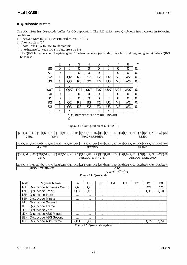
■ Q-subcode Buffers
The AK4118A has Q-subcode buffer for CD application. The AK4118A takes Q-subcode into registers in following
conditions.
1. The sync word (S0,S1) is constructed at least 16 “0”s.
2. The start bit is “1”.
3. Those 7bits Q-W follows to the start bit.
4. The distance between two start bits are 8-16 bits.
The QINT bit in the control register goes “1” when the new Q-subcode differs from old one, and goes “0” when QINT
bit is read.
1 2 3 4 5 6 7 8 *
S0 0 0 0 0 0 0 0 0 0…
S1 0 0 0 0 0 0 0 0 0…
S2 1 Q2 R2 S2 T2 U2 V2 W2 0…
S3 1 Q3 R3 S3 T3 U3 V3 W3 0…
: : : : : : : : : :
S97 1 Q97 R97 S97 T97 U97 V97 W97 0…
S0 0 0 0 0 0 0 0 0 0…
S1 0 0 0 0 0 0 0 0 0…
S2 1 Q2 R2 S2 T2 U2 V2 W2 0…
S3 1 Q3 R3 S3 T3 U3 V3 W3 0…
: : : : : : : : : : (*) number of "0" : min=0; max=8.
Figure 23. Configuration of U- bit (CD)
Q2 Q3 Q4 Q5 Q6 Q7 Q8 Q9 Q10 Q11 Q12 Q13 Q14 Q15 Q16 Q17 Q18 Q19 Q20 Q21 Q22 Q23 Q24 Q25
CTRL ADRS TRACK NUMBER INDEX
Q26 Q27 Q28 Q29 Q30 Q31 Q32 Q33 Q34 Q35 Q36 Q37 Q38 Q39 Q40 Q41 Q42 Q43 Q44 Q45 Q46 Q47 Q48 Q49
MINUTE SECOND FRAME
Q50 Q51 Q52 Q53 Q54 Q55 Q56 Q57 Q58 Q59 Q60 Q61 Q62 Q63 Q64 Q65 Q66 Q67 Q68 Q69 Q70 Q71 Q72 Q73
ZERO ABSOLUTE MINUTE ABSOLUTE SECOND
Q74 Q75 Q76 Q77 Q78 Q79 Q80 Q81 Q82 Q83 Q84 Q85 Q86 Q87 Q88 Q89 Q90 Q91 Q92 Q93 Q94 Q95 Q96 Q97
ABSOLUTE FRAME CRC
G(x)=x16+x12+x5+1
Figure 24. Q-subcode
Addr Register Name D7 D6 D5 D4 D3 D2 D1 D0
16H Q-subcode Address / Control Q9 Q8 … … … … Q3 Q2
17H Q-subcode Track Q17 Q16 … … … … Q11 Q10
18H Q-subcode Index … … … … … … … …
19H Q-subcode Minute … … … … … … … …
1AH Q-subcode Second … … … … … … … …
1BH Q-subcode Frame … … … … … … … …
1CH Q-subcode Zero … … … … … … … …
1DH Q-subcode ABS Minute … … … … … … … …
1EH Q-subcode ABS Second … … … … … … … …
1FH Q-subcode ABS Frame Q81 Q80 … … … … Q75 Q74
Figure 25. Q-subcode register
↑
Q

[AK4118A]
MS1130-E-03 2013/09
- 27 -
■ Error Handling
The following nine events cause the INT0 and INT1 pins to show the status of the interrupt condition. When the PLL is
OFF (Clock Operation Mode 1), INT0 and INT1 pins go to “L”.
1. UNLCK : PLL unlock state detect
“1” when the PLL loses lock. The AK4118A loses lock when the distance between two preamble is
not correct or when those preambles are not correct.
2. PAR : Parity error or bi-phase coding error detection
“1” when parity error or bi-phase coding error is detected, updated every sub-frame cycle.
3. AUTO : Non-Linear PCM or DTS-CD Bit Stream detection
The OR function of NPCM and DTSCD bits is available at the AUTO bit.
4. V : Validity flag detection
“1” when validity flag is detected. Updated every sub-frame cycle.
5. AUDION : Non-audio detection
“1” when the “AUDION” bit in recovered channel status indicates “1”. Updated every block cycle.
6. STC : Sampling frequency or pre-emphasis information change detection
When either FS3-0 bit or PEM bit is changed, it maintains “1” during 1 sub-frame.
7. QINT : U-bit Sync flag
“1” when the Q-subcode differs from the old one. Updated every sync code cycle for Q-subcode.
8. CINT : Channel status sync flag
“1” when received C bit differs from the old one. Updated every block cycle.
9. DAT : DAT Start ID detect
“1” when the category code indicates “DAT” and “DAT Start ID” is detected. When DCNT bit is
“1”, it does not indicate “1” even if “DAT Start ID” is detected again within “3841 x LRCK”.
When “DAT Start ID” is detected again after “3840 x LRCK” passed, it indicates “1”. When
DCNT bit is “0”, it indicates “1” every “DAT Start ID” detection.

[AK4118A]
MS1130-E-03 2013/09
- 28 -
1. Parallel control mode
In parallel control mode, the INT0 pin outputs the ORed signal between UNLCK and PAR. The INT1 pin outputs the
ORed signal between AUTO and AUDION. Once the INT0 pin goes to “H”, it maintains “H” for 1024/fs cycles after the
all error events are removed. Table 15 shows the state of each output pins when the INT0/1 pin is “H”.
Event Pin
UNLCK PAR AUTO AUDION INT0 INT1 SDTO V
1 x x x H
Note 14
L L
0 1 x x Previous Data Output
0 0 x x L Output Output
x x 1 x
Note 15 H
Note 16 Note 17 x x x 1
x x 0 0 L
Note 14. The INT1 pin outputs “L” or “H” in accordance with the ORed signal between AUTO and AUDION.
Note 15. The INT0 pin outputs “L” or “H” in accordance with the ORed signal between UNLCK and PAR.
Note 16. The SDTO pin outputs “L”, “Previous Data” or “Normal Data” in accordance with the ORed signal between
UNLCK and PAR.
Note 17. The VIN pin outputs “L” or “Normal operation” in accordance with the ORed signal between PAR and
UNCLK.
Table 15. Error Handling in parallel control mode (x: Don’t care)
2. Serial control mode
In serial control mode, the INT1 and INT0 pins output an ORed signal based on the above nine interrupt events. When
masked, the interrupt event does not affect the operation of the INT1-0 pins (the masks do not affect the registers in 07H
and DAT bit). Once the INT0 pin goes to “H”, it remains “H” for 1024/fs (this value can be changed with the EFH1-0
bits) after all events not masked by mask bits are cleared. The INT1 pin immediately goes to “L” when those events are
cleared.
UNLCK, PAR, AUTO, AUDION and V bits in Address=07H indicate the interrupt status events above in real time. Once
QINT, CINT and DAT bits goes to “1”, it stays “1” until the register is read.
When the AK4118A loses lock, the channel status bit, user bit, Pc and Pd are initialized. In this initial state, The INT0 pin
outputs the ORed signal between UNLCK and PAR bits. The INT1 pin outputs the ORed signal between AUTO and
AUDION bits.
Event Pin
UNLCK PAR Others SDTO V TX
1 x x L L Output
0 1 x Previous Data Output Output
x x x Output Output Output
Table 16. Error Handling in serial control mode (x: Don’t care)

[AK4118A]
MS1130-E-03 2013/09
- 29 -
Error
(UNLOCK, PAR,..)
INT1 pin
SDTO
(UNLOCK)
MCKO,BICK,LRCK
(UNLOCK)
Previous Data
Register
(PAR,CINT,QINT) Hold ”1”
Command READ 06H
MCKO,BICK,LRCK
(except UNLOCK)
(fs: around 5kHz)
SDTO
(PAR error)
Hold Time = 0
Reset
(Error)
SDTO
(others)
Normal Operation
INT0 pin Hold Time (max: 4096/fs)
Register
(others)
Free Run
Vpin
(UNLOCK)
Vpin
(except UNLOCK)
Figure 26. INT0/1 pin Timing

[AK4118A]
MS1130-E-03 2013/09
- 30 -
INT0/1 pin ="H"
No
Yes
Yes
Initialize
PD pin ="L" to "H"
Read 06H
Mute DAC output
Read 06H
No
(Each Error Handling)
Read 06H(Resets registers)
INT0/1 pin ="H"
ReleaseMuting
Figure 27. Error Handling Sequence Example 1

[AK4118A]
MS1130-E-03 2013/09
- 31 -
INT1 pin ="H"
No
Yes
Initialize
PD pin ="L" to "H"
Read 06H
Read 06Hand
Detect QSUB= “1”
No
(Read Q-buffer)
New datais valid
INT1 pin ="L"
QCRC = “0”
Yes
Yes
New datais invalid
No
Figure 28. Error Handling Sequence Example (for Q/CINT)

[AK4118A]
MS1130-E-03 2013/09
- 32 -
■ Audio Serial Interface Format
The DIF0, DIF1 and DIF2 pins can select eight serial data formats as shown in Table 17. In all formats the serial data is
MSBfirst, 2's compliment format. The SDTO is clocked out on the falling edge of BICK and the DAUX is latched on
the rising edge of BICK. BICK outputs 64fs clock in Mode 05. Mode 67 are Slave Modes, and BICK is available up to
128fs at fs=48kHz. In the format equal or less than 20bit (Mode0-2), LSBs in sub-frame are truncated. In Mode 3-7, the
last 4LSBs are auxiliary data (Figure 29).
When the Parity Error occurs in a sub-frame, the AK4118A continues to output the last normal sub-frame data from
SDTO repeatedly until the error is removed. When the Unlock Error occurs, the AK4118A outputs “0” data from the
SDTO pin. In case of using the DAUX pin, the data is transformed and output from SDTO. The DAUX pin is used in
Clock Operation Mode 1/3 and unlock state of Mode 2.
The input data format to DAUX should be left justified except in Mode5 and Mode7 (Table 17). In Mode5 or Mode7,
both the input data format of DAUX and output data format of SDTO are I2S. Mode6 and Mode7 are Slave Mode that is
corresponding to the Master Mode of Mode4 and Mode5. In salve Mode, LRCK and BICK should be fed with
synchronizing to MCKO1/2.
0 3 4 7 8 11 12 27 28 29 30 31
preamble Aux.
LSB MSB
V U C P
sub-frame of IEC60958
0 23
AK4118 Audio Data (MSB First)
LSB MSB
Figure 29. Bit Configuration
Mode DIF2 DIF1 DIF0 DAUX SDTO LRCK BICK
I/O I/O
0 0 0 0 24bit, Left justified 16bit, Right justified H/L O 64fs O
1 0 0 1 24bit, Left justified 18bit, Right justified H/L O 64fs O
2 0 1 0 24bit, Left justified 20bit, Right justified H/L O 64fs O
3 0 1 1 24bit, Left justified 24bit, Right justified H/L O 64fs O
4 1 0 0 24bit, Left justified 24bit, Left justified H/L O 64fs O
5 1 0 1 24bit, I2S 24bit, I
2S L/H O 64fs O
6 1 1 0 24bit, Left justified 24bit, Left justified H/L I 64-128fs I (default)
7 1 1 1 24bit, I2S 24bit, I
2S L/H I 64-128fs I
Table 17. Audio Data Format

[AK4118A]
MS1130-E-03 2013/09
- 33 -
LRCK(0)
BICK
(0:64fs)
SDTO(0)
0 1 2 31 0 1
15:MSB, 0:LSB
Lch Data Rch Data
15 1716 1531 0 1 2 1716
0 1 01 15 141415
Figure 30. Mode 0 Timing
LRCK(0)
BICK
(0:64fs)
SDTO(0)
0 1 2 31 0 1
23:MSB, 0:LSB
Lch Data Rch Data
9 1110 931 0 1 2 1110
0 1 01
12
21 202021
12
2223 2223
Figure 31. Mode 3 Timing
LRCK
BICK
(64fs)
SDTO(0)
0 1 2 31 0 1
23:MSB, 0:LSB
Lch Data Rch Data
21 2322 2131 0 1 2 2322
23 222
24
1 001
24
212223 3 2 23 22
Figure 32. Mode 4/6 Timing Mode4: LRCK, BICK (Output)
Mode6: LRCK, BICK (Input)
LRCK
BICK
(64fs)
SDTO(0)
0 1 2 31 0 1
23:MSB, 0:LSB
Lch Data Rch Data
2322 2131 0 1 2 2322
23 22
24
1 0
24
3 2 23
25
2 01212223
25
Figure 33. Mode 5/7 Timing Mode5: LRCK, BICK (Output)
Mode7: LRCK, BICK (Input)

[AK4118A]
MS1130-E-03 2013/09
- 34 -
■ GPIO Controller
The AK4118A has 8 input/output port pins. Set GP0~GP7 pins by GPDR register for data direction, GPSCR register for
the pin level setting and GPLR register for pin level reading. Table 18 ~ Table 21 show the pin state at setting or internal
node state of GPIO registers, BCU bit, TX1E/TX0E bit and VIN E bit.
VIN GP0
Register Setting Register Read Internal Node
Pin State VIN GP0 pin VINE GPE GPDR GPSCR GPLR VIN I
1 x x x L VIN I VIN
0 x 0 x GPI L I GPI
0 x 1 Valid GPSCR L O GPSCR
Table 18. VINGP0 pin and Internal Statement (x: Don’t care)
GP1
Register Setting Register Read
Pin State GP1 pin GPE GPDR GPSCR GPLR
x 0 x GPI I GPI
x 1 x GPSCR O GPSCR
Table 19. GP1 pin and Internal Statement (x: Don’t care)
TX0/1 GP2/3
Register Setting Register Read
Pin State TX GP pin TX E GPE GPDR GPSCR GPLR
1 x x x L O RX
0 0 x x L O L
0 1 0 x GPI I GPI
0 1 1 Valid GPSCR O GPSCR
Table 20. TX0/1 GP2/3 pin and Internal Statement (x: Don’t care)
B/C/U/VOUT GP4/5/6/7
Register Setting Register Read
Pin State BCUV GP pin BCU GPE GPDR GPSCR GPLR
1 x x x L O BCUV OUT
0 0 x x Data Hold O L
0 1 0 x GPI I GPI
0 1 1 Valid GPSCR O GPSCR
Table 21. B/C/U/VOUT GP4/5/6/7 pin and Internal Statement (x: Don’t care)
[AK4118A]
MS1130-E-03 2013/09
- 35 -
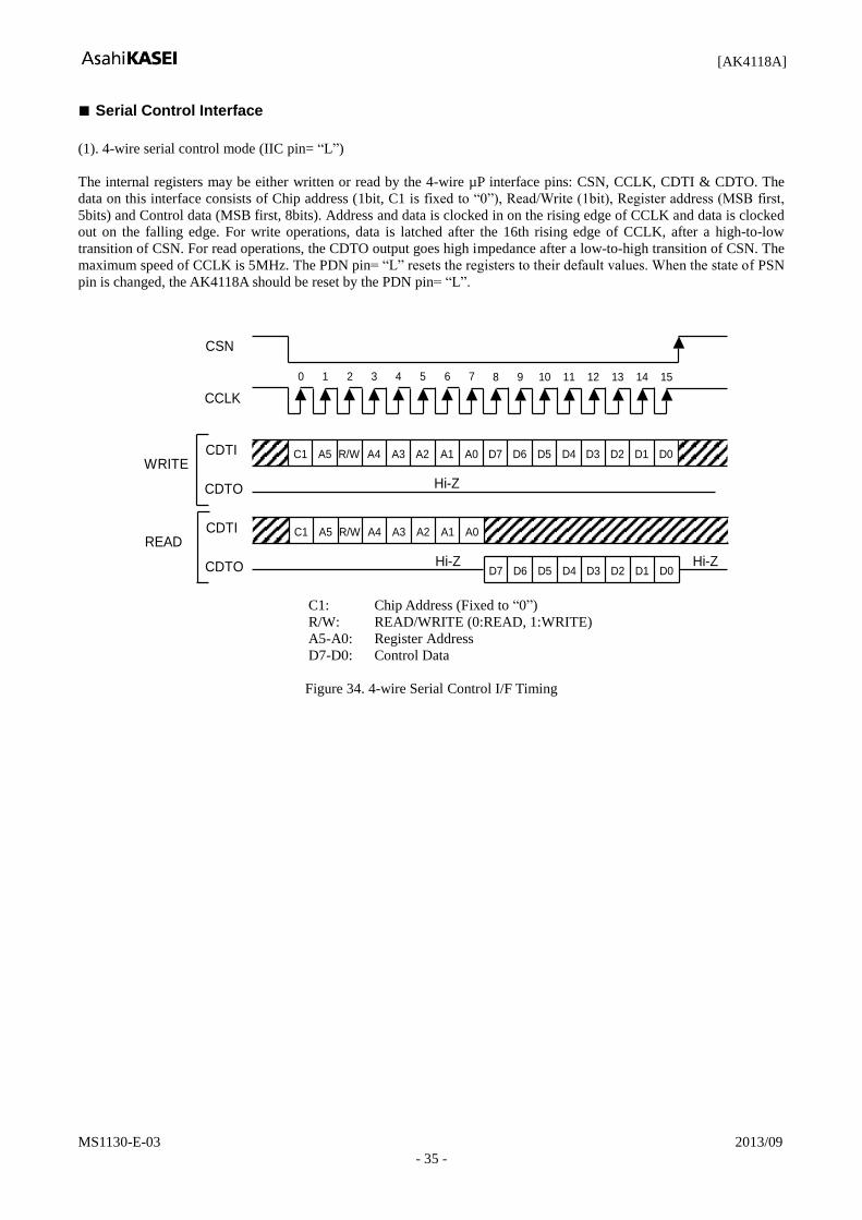
■ Serial Control Interface
(1). 4-wire serial control mode (IIC pin= “L”)
The internal registers may be either written or read by the 4-wire µP interface pins: CSN, CCLK, CDTI & CDTO. The
data on this interface consists of Chip address (1bit, C1 is fixed to “0”), Read/Write (1bit), Register address (MSB first,
5bits) and Control data (MSB first, 8bits). Address and data is clocked in on the rising edge of CCLK and data is clocked
out on the falling edge. For write operations, data is latched after the 16th rising edge of CCLK, after a hightolow
transition of CSN. For read operations, the CDTO output goes high impedance after a lowtohigh transition of CSN. The
maximum speed of CCLK is 5MHz. The PDN pin= “L” resets the registers to their default values. When the state of PSN
pin is changed, the AK4118A should be reset by the PDN pin= “L”.
CDTI
CCLK
CSN
C1
0 1 2 3 4 5 6 7 8 9 10 11 12 13 14 15
D4 D5 D6 D7 A1 A2 A3 A4 R/W A5 A0 D0 D1 D2 D3
CDTO Hi-Z
WRITE
CDTI C1 D4 D5 D6 D7 A1 A2 A3 A4 R/W A5 A0 D0 D1 D2 D3
CDTO Hi-Z
READ
D4 D5 D6 D7 D0 D1 D2 D3 Hi-Z
C1: Chip Address (Fixed to “0”)
R/W: READ/WRITE (0:READ, 1:WRITE)
A5-A0: Register Address
D7-D0: Control Data
Figure 34. 4-wire Serial Control I/F Timing

[AK4118A]
MS1130-E-03 2013/09
- 36 -
(2). I2C bus control mode (IIC pin= “H”)
The AK4118A supports High speed mode I2C-bus (max: 400kHz).
(2)-1. Data transfer
In order to access any IC devices on the I²C BUS, input a start condition first, followed by a single Slave address that
includes the Device Address. IC devices on the BUS compare this Slave address with their own addresses and the IC
device that has identical address with the Slave-address generates an acknowledgement. An IC device with the identical
address executes either a read or write operation. After the command execution, input Stop condition.
(2)-1-1. Data Change
Change the data on the SDA line while SCL line is “L”. SDA line condition must be stable and fixed while the clock is
“H”. Change the Data line condition between “H” and “L” only when the clock signal on the SCL line is “L”. Change the
SDA line condition while SCL line is “H” only when the start condition or stop condition is input.
SCL
SDA
DATA LINESTABLE :
DATA VALID
CHANGEOF DATAALLOWED
Figure 35. Data Transfer
(2)-1-2. START and STOP condition
Start condition is generated by the transition of “H” to “L” on the SDA line while the SCL line is “H”. All instructions are
initiated by Start condition. Stop condition is generated by the transition of “L” to “H” on SDA line while SCL line is
“H”. All instructions end by Stop condition.
SCL
SDA
STOP CONDITIONSTART CONDITION
Figure 36. START and STOP condition

[AK4118A]
MS1130-E-03 2013/09
- 37 -
(2)-1-3. Acknowledge
An external device that is sending data to the AK4118A releases the SDA line (“H”) after receiving one-byte of data. An
external device that receives data from the AK4118A then sets the SDA line to “L” at the next clock. This operation is
called “acknowledgement”, and it enables verification that the data transfer has been properly executed. The AK4118A
generates an acknowledgement upon receipt of Start condition and Slave address. For a write instruction, an
acknowledgement is generated whenever receipt of each byte is completed. For a read instruction, succeeded by
generation of an acknowledgement, the AK4118A releases the SDA line after outputting data at the designated address,
and it monitors the SDA line condition. When the Master side generates an acknowledgement without sending a Stop
condition, the AK4118A outputs data at the next address location. When no acknowledgement is generated, the AK4118A
ends data output (not acknowledged).
SCL FROMMASTER
acknowledge
DATAOUTPUT BYTRANSMITTER
DATAOUTPUT BYRECEIVER
1 98
STARTCONDITION
Clock pulsefor acknowledge
not acknowledge
Figure 37. Acknowledge on the I
2C-bus
(2)-1-4. The First Byte
The First Byte which includes the Slave-address is input after the Start condition is set, and a target IC device that will be
accessed on the bus is selected by the Slave-address. The Slave-address is configured with the upper 7-bits. Data of the
upper 5-bits is “00100”. The next 2 bits are address bits that select the desired IC which are set by the CAD1 and CAD0
pins. When the Slave-address is inputted, an external device that has the identical device address generates an
acknowledgement and instructions are then executed. The 8th bit of the First Byte (lowest bit) is allocated as the R/W Bit.
When the R/W Bit is “1”, the read instruction is executed, and when it is “0”, the write instruction is executed.
0 0 1 0 0 CAD1 CAD0 R/W
(Those CAD1/0 should match with CAD1/0 pins.)
Figure 38. The First Byte

[AK4118A]
MS1130-E-03 2013/09
- 38 -
(2)-2. WRITE Operations
Set R/W bit = “0” for the WRITE operation of the AK4118A.
After receipt the start condition and the first byte, the AK4118A generates an acknowledge, and awaits the second byte
(register address). The second byte consists of the address for control registers of the AK4118A. The format is MSB first,
and those most significant 3-bits are “Don’t care”.
0 0 A5 A4 A3 A2 A1 A0
(*: Don’t care)
Figure 39. The Second Byte
After receipt the second byte, the AK4118A generates an acknowledge, and awaits the third byte. Those data after the
second byte contain control data. The format is MSB first, 8bits.
D7 D6 D5 D4 D3 D2 D1 D0
Figure 40. Byte structure after the second byte
The AK4118A is capable of more than one byte write operation in one sequence.
After receipt of the third byte, the AK4118A generates an acknowledge, and awaits the next data again. The master can
transmit more than one words instead of terminating the write cycle after the first data word is transferred. After the
receipt of each data, the internal 5bits address counter is incremented by one, and the next data is taken into next address
automatically. If the address exceed 1FH prior to generating the stop condition, the address counter will “roll over” to
00H and the previous data will be overwritten.
SDA
START
ACK
ACK
S
SlaveAddress
ACK
RegisterAddress(n)
Data(n)
P
STOP
Data(n+x)
ACK
Data(n+1)
Figure 41. WRITE Operation

[AK4118A]
MS1130-E-03 2013/09
- 39 -
(2)-3. READ Operations
Set R/W bit = “1” for the READ operation of the AK4118A.
After transmission of a data, the master can read next address’s data by generating the acknowledge instead of
terminating the write cycle after the receipt the first data word. After the receipt of each data, the internal 5bits address
counter is incremented by one, and the next data is taken into next address automatically. If the address exceed 1FH prior
to generating the stop condition, the address counter will “roll over” to 00H and the previous data will be overwritten.
The AK4118A supports two basic read operations: CURRENT ADDRESS READ and RANDOM READ.
(2)-3-1. CURRENT ADDRESS READ
The AK4118A contains an internal address counter that maintains the address of the last word accessed, incremented by
one. Therefore, if the last access (either a read or write) was to address “n”, the next CURRENT READ operation would
access data from the address “n+1”.
After receipt of the slave address with R/W bit set to “1”, the AK4118A generates an acknowledge, transmits 1byte data
which address is set by the internal address counter and increments the internal address counter by 1. If the master does
not generate an acknowledge but generate the stop condition, the AK4118A discontinues transmission.
SDA
START
ACK
ACK
S
SlaveAddress
ACK
Data(n) Data(n+1)
P
STOP
Data(n+x)
ACK
Data(n+2)
Figure 42. CURRENT ADDRESS READ
(2)-3-2. RANDOM READ
Random read operation allows the master to access any memory location at random. Prior to issuing the slave address
with the R/W bit set to “1”, the master must first perform a “dummy” write operation.
The master issues start condition, slave address(R/W=“0”) and then the register address to read. After the register
address’s acknowledge, the master immediately reissues start condition and the slave address with the R/W bit set to “1”.
Then the AK4118A generates an acknowledge, 1byte data and increments the internal address counter by 1. If the master
does not generate an acknowledge but generate the stop condition, the AK4118A discontinues transmission.
SDA
START
ACK
ACK
S S
START
SlaveAddress
WordAddress(n)
SlaveAddress
ACK
Data(n)
ACK
P
STOP
Data(n+x)
ACK
Data(n+1)
Figure 43. RANDOM READ

[AK4118A]
MS1130-E-03 2013/09
- 40 -
■ Register Map
Addr Register Name D7 D6 D5 D4 D3 D2 D1 D0
00H CLK & Power Down
Control CS12 BCU CM1 CM0 OCKS1 OCKS0 PWN RSTN
01H Format & Deem Control MONO DIF2 DIF1 DIF0 DEAU DEM1 DEM0 DFS
02H Input/ Output Control 0 TX1E OPS12 OPS11 OPS10 TX0E OPS02 OPS01 OPS00
03H Input/ Output Control 1 EFH1 EFH0 UDIT TLR DIT IPS2 IPS1 IPS0
04H INT0 MASK MQIT0 MAUT0 MCIT0 MULK0 MDTS0 MPE0 MAUD0 MPAR0
05H INT1 MASK MQIT1 MAUT1 MCIT1 MULK1 MDTS1 MPE1 MAUD1 MPAR1
06H Receiver status 0 QINT AUTO CINT UNLCK DTSCD PEM AUDION PAR
07H Receiver status 1 FS3 FS2 FS1 FS0 0 V QCRC CCRC
08H RX Channel Status Byte 0 CR7 CR6 CR5 CR4 CR3 CR2 CR1 CR0
09H RX Channel Status Byte 1 CR15 CR14 CR13 CR12 CR11 CR10 CR9 CR8
0AH RX Channel Status Byte 2 CR23 CR22 CR21 CR20 CR19 CR18 CR17 CR16
0BH RX Channel Status Byte 3 CR31 CR30 CR29 CR28 CR27 CR26 CR25 CR24
0CH RX Channel Status Byte 4 CR39 CR38 CR37 CR36 CR35 CR34 CR33 CR32
0DH TX Channel Status Byte 0 CT7 CT6 CT5 CT4 CT3 CT2 CT1 CT0
0EH TX Channel Status Byte 1 CT15 CT14 CT13 CT12 CT11 CT10 CT9 CT8
0FH TX Channel Status Byte 2 CT23 CT22 CT21 CT20 CT19 CT18 CT17 CT16
10H TX Channel Status Byte 3 CT31 CT30 CT29 CT28 CT27 CT26 CT25 CT24
11H TX Channel Status Byte 4 CT39 CT38 CT37 CT36 CT35 CT34 CT33 CT32
12H Burst Preamble Pc Byte 0 PC7 PC6 PC5 PC4 PC3 PC2 PC1 PC0
13H Burst Preamble Pc Byte 1 PC15 PC14 PC13 PC12 PC11 PC10 PC9 PC8
14H Burst Preamble Pd Byte 0 PD7 PD6 PD5 PD4 PD3 PD2 PD1 PD0
15H Burst Preamble Pd Byte 1 PD15 PD14 PD13 PD12 PD11 PD10 PD9 PD8
16H Q-subcode Address / Control Q9 Q8 Q7 Q6 Q5 Q4 Q3 Q2
17H Q-subcode Track Q17 Q16 Q15 Q14 Q13 Q12 Q11 Q10
18H Q-subcode Index Q25 Q24 Q23 Q22 Q21 Q20 Q19 Q18
19H Q-subcode Minute Q33 Q32 Q31 Q30 Q29 Q28 Q27 Q26
1AH Q-subcode Second Q41 Q40 Q39 Q38 Q37 Q36 Q35 Q34
1BH Q-subcode Frame Q49 Q48 Q47 Q46 Q45 Q44 Q43 Q42
1CH Q-subcode Zero Q57 Q56 Q55 Q54 Q53 Q52 Q51 Q50
1DH Q-subcode ABS Minute Q65 Q64 Q63 Q62 Q61 Q60 Q59 Q58
1EH Q-subcode ABS Second Q73 Q72 Q71 Q70 Q69 Q68 Q67 Q66
1FH Q-subcode ABS Frame Q81 Q80 Q79 Q78 Q77 Q76 Q75 Q74

[AK4118A]
MS1130-E-03 2013/09
- 41 -
Addr Register Name D7 D6 D5 D4 D3 D2 D1 D0
20H GPE GPE RXDETE VINE FAST EXCKMD DCNT DTS16 DTS14
21H GPDR IO7 IO6 IO5 IO4 IO3 IO2 IO1 IO0
22H GPSCR CS7 SC6 CS5 SC4 SC3 SC2 SC1 CS0
23H GPLR GPL7 GPL 6 GPL 5 GPL 4 GPL 3 GPL 2 GPL 1 GPL 0
24H DAT Mask & DTS Detect XMCK DIV MED1 MDR0 MSTC1 MSTC0 MDAT1 MDAT0
25H RX Detect RXDE7 RXDE6 RXDE5 RXDE4 RXDE3 RXDE2 RXDE1 RXDE0
26H STC & DAT Detect 0 0 0 0 0 0 STC DAT
27H RX Channel Status Byte 5 0 0 0 0 0 0 CR41 CR40
28H TX Channel Status Byte 5 0 1 0 0 0 0 CT41 CT40
Note: When the PDN pin goes “L”, the registers are initialized to their default values.
When RSTN bit goes “0”, the internal timing is reset and the registers are initialized to their default values.
All data can be written to the register even if PWN bit is “0”.

[AK4118A]
MS1130-E-03 2013/09
- 42 -
■ Register Definitions
Reset & Initialize
Addr Register Name D7 D6 D5 D4 D3 D2 D1 D0
00H CLK & Power Down Control CS12 BCU CM1 CM0 OCKS1 OCKS0 PWN RSTN
R/W R/W R/W R/W R/W R/W R/W R/W R/W
Default 0 1 0 0 0 0 1 1
RSTN: Timing Reset & Register Initialize
0: Reset & Initialize
1: Normal Operation
PWN: Power Down
0: Power Down
1: Normal Operation
OCKS10: Master Clock Frequency Select
CM1-0: Master Clock Operation Mode Select
BCU: Block start & C/U Output Mode
When BCU=1, the three Output Pins(BOUT, COUT, UOUT) become to be enabled.
The block signal goes high at the start of frame 0 and remains high until the end of frame 31.
CS12: Channel Status Select
0: Channel 1
1: Channel 2
Selects which channel status is used to derive C-bit buffers, AUDION, PEM, FS3, FS2, FS1, FS0,
Pc and Pd. The deemphasis filter is controlled by channel 1 in the Parallel Mode.
Format & Deemphasis Control
Addr Register Name D7 D6 D5 D4 D3 D2 D1 D0
01H Format & Deem Control MONO DIF2 DIF1 DIF0 DEAU DEM1 DEM0 DFS
R/W R/W R/W R/W R/W R/W R/W R/W R/W
Default 0 1 1 0 1 0 1 0
DFS: 96kHz Deemphasis Control
DEM10: 32, 44.1, 48kHz Deemphasis Control (Table 11)
DEAU: Deemphasis Auto Detect Enable
0: Disable
1: Enable
DIF20: Audio Data Format Control (Table 17)
MONO: Double sampling frequency mode enable
0: Stereo mode
1: Mono mode

[AK4118A]
MS1130-E-03 2013/09
- 43 -
Input/Output Control
Addr Register Name D7 D6 D5 D4 D3 D2 D1 D0
02H Input/ Output Control 0 TX1E OPS12 OPS11 OPS10 TX0E OPS02 OPS01 OPS00
R/W R/W R/W R/W R/W R/W R/W R/W R/W
Default 1 0 0 0 1 0 0 0
OPS0200: Output Through Data Select for TX0 pin
OPS1210: Output Through Data Select for TX1 pin
TX0E: TX0 Output Enable
0: Disable. TX0 outputs “L”.
1: Enable
TX1E: TX1 Output Enable
0: Disable. TX1 outputs “L”.
1: Enable
Addr Register Name D7 D6 D5 D4 D3 D2 D1 D0
03H Input/ Output Control 1 EFH1 EFH0 UDIT TLR DIT IPS2 IPS1 IPS0
R/W R/W R/W R/W R/W R/W R/W R/W R/W
Default 0 1 0 0 1 0 0 0
IPS20: Input Recovery Data Select
DIT: Through data/Transmit data select for TX1 pin
0: Through data (RX data).
1: Transmit data (DAUX data).
TLR: Double sampling frequency mode channel select for DIT(stereo)
0: L channel
1: R channel
UDIT: U bit control for DIT
0: U bit is fixed to “0”
1: Recovered U bit is used for DIT (loop mode for U bit)
EFH10: Interrupt 0 Pin Hold Count Select
00: 512 LRCK
01: 1024 LRCK
10: 2048 LRCK
11: 4096 LRCK

[AK4118A]
MS1130-E-03 2013/09
- 44 -
Mask Control for INT0
Addr Register Name D7 D6 D5 D4 D3 D2 D1 D0
04H INT0 MASK MQI0 MAT0 MCI0 MUL0 MDTS0 MPE0 MAN0 MPR0
R/W R/W R/W R/W R/W R/W R/W R/W R/W
Default 1 1 1 0 1 1 1 0
MPR0: Mask Enable for PAR bit
MAN0: Mask Enable for AUDN bit
MPE0: Mask Enable for PEM bit
MDTS0: Mask Enable for DTSCD bit
MUL0: Mask Enable for UNLOCK bit
MCI0: Mask Enable for CINT bit
MAT0: Mask Enable for AUTO bit
MQI0: Mask Enable for QINT bit
0: Mask disable
1: Mask enable
Mask Control for INT1
Addr Register Name D7 D6 D5 D4 D3 D2 D1 D0
05H INT1 MASK MQI1 MAT1 MCI1 MUL1 MDTS1 MPE1 MAN1 MPR1
R/W R/W R/W R/W R/W R/W R/W R/W R/W
Default 1 0 1 1 0 1 0 1
MPR1: Mask Enable for PAR bit
MAN1: Mask Enable for AUDN bit
MPE1: Mask Enable for PEM bit
MDTS1: Mask Enable for DTSCD bit
MUL1: Mask Enable for UNLOCK0 bit
MCI1: Mask Enable for CINT bit
MAT1: Mask Enable for AUTO bit
MQI1: Mask Enable for QINT bit
0: Mask disable
1: Mask enable
[AK4118A]
MS1130-E-03 2013/09
- 45 -
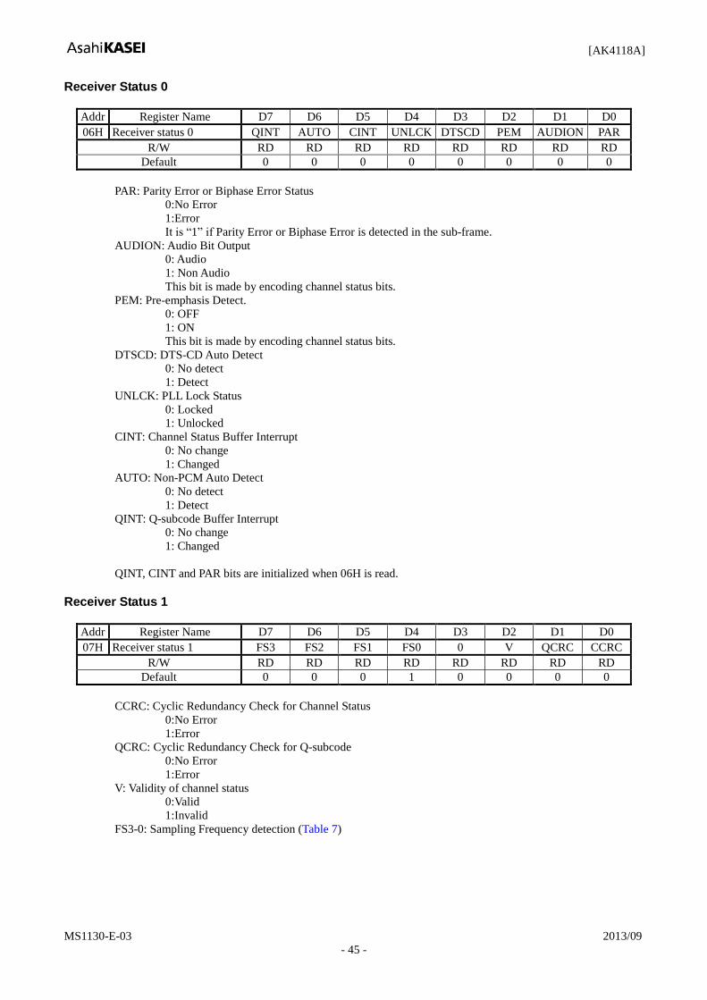
Receiver Status 0
Addr Register Name D7 D6 D5 D4 D3 D2 D1 D0
06H Receiver status 0 QINT AUTO CINT UNLCK DTSCD PEM AUDION PAR
R/W RD RD RD RD RD RD RD RD
Default 0 0 0 0 0 0 0 0
PAR: Parity Error or Biphase Error Status
0:No Error
1:Error
It is “1” if Parity Error or Biphase Error is detected in the subframe.
AUDION: Audio Bit Output
0: Audio
1: Non Audio
This bit is made by encoding channel status bits.
PEM: Preemphasis Detect.
0: OFF
1: ON
This bit is made by encoding channel status bits.
DTSCD: DTS-CD Auto Detect
0: No detect
1: Detect
UNLCK: PLL Lock Status
0: Locked
1: Unlocked
CINT: Channel Status Buffer Interrupt
0: No change
1: Changed
AUTO: Non-PCM Auto Detect
0: No detect
1: Detect
QINT: Q-subcode Buffer Interrupt
0: No change
1: Changed
QINT, CINT and PAR bits are initialized when 06H is read.
Receiver Status 1
Addr Register Name D7 D6 D5 D4 D3 D2 D1 D0
07H Receiver status 1 FS3 FS2 FS1 FS0 0 V QCRC CCRC
R/W RD RD RD RD RD RD RD RD
Default 0 0 0 1 0 0 0 0
CCRC: Cyclic Redundancy Check for Channel Status
0:No Error
1:Error
QCRC: Cyclic Redundancy Check for Q-subcode
0:No Error
1:Error
V: Validity of channel status
0:Valid
1:Invalid
FS30: Sampling Frequency detection (Table 7)

[AK4118A]
MS1130-E-03 2013/09
- 46 -
Receiver Channel Status
Addr Register Name D7 D6 D5 D4 D3 D2 D1 D0
08H RX Channel Status Byte 0 CR7 CR6 CR5 CR4 CR3 CR2 CR1 CR0
09H RX Channel Status Byte 1 CR15 CR14 CR13 CR12 CR11 CR10 CR9 CR8
0AH RX Channel Status Byte 2 CR23 CR22 CR21 CR20 CR19 CR18 CR17 CR16
0BH RX Channel Status Byte 3 CR31 CR30 CR29 CR28 CR27 CR26 CR25 CR24
0CH RX Channel Status Byte 4 CR39 CR38 CR37 CR36 CR35 CR34 CR33 CR32
27H RX Channel Status Byte 5 0 0 0 0 0 0 CR41 CR40
R/W RD
Default Not initialized
CR410: Receiver Channel Status Byte 50
Transmitter Channel Status
Addr Register Name D7 D6 D5 D4 D3 D2 D1 D0
0DH TX Channel Status Byte 0 CT7 CT6 CT5 CT4 CT3 CT2 CT1 CT0
0EH TX Channel Status Byte 1 CT15 CT14 CT13 CT12 CT11 CT10 CT9 CT8
0FH TX Channel Status Byte 2 CT23 CT22 CT21 CT20 CT19 CT18 CT17 CT16
10H TX Channel Status Byte 3 CT31 CT30 CT29 CT28 CT27 CT26 CT25 CT24
11H TX Channel Status Byte 4 CT39 CT38 CT37 CT36 CT35 CT34 CT33 CT32
28H TX Channel Status Byte 5 0 1 0 0 0 0 CT41 CT40
R/W R/W
Default 0
CT410: Transmitter Channel Status Byte 50
Burst Preamble Pc/Pd in non-PCM encoded Audio Bitstreams
Addr Register Name D7 D6 D5 D4 D3 D2 D1 D0
12H Burst Preamble Pc Byte 0 PC7 PC6 PC5 PC4 PC3 PC2 PC1 PC0
13H Burst Preamble Pc Byte 1 PC15 PC14 PC13 PC12 PC11 PC10 PC9 PC8
14H Burst Preamble Pd Byte 0 PD7 PD6 PD5 PD4 PD3 PD2 PD1 PD0
15H Burst Preamble Pd Byte 1 PD15 PD14 PD13 PD12 PD11 PD10 PD9 PD8
R/W RD
Default Not initialized
PC150: Burst Preamble Pc Byte 0 and 1
PD150: Burst Preamble Pd Byte 0 and 1

[AK4118A]
MS1130-E-03 2013/09
- 47 -
Q-subcode Buffer
Addr Register Name D7 D6 D5 D4 D3 D2 D1 D0
16H Q-subcode Address / Control Q9 Q8 Q7 Q6 Q5 Q4 Q3 Q2
17H Q-subcode Track Q17 Q16 Q15 Q14 Q13 Q12 Q11 Q10
18H Q-subcode Index Q25 Q24 Q23 Q22 Q21 Q20 Q19 Q18
19H Q-subcode Minute Q33 Q32 Q31 Q30 Q29 Q28 Q27 Q26
1AH Q-subcode Second Q41 Q40 Q39 Q38 Q37 Q36 Q35 Q34
1BH Q-subcode Frame Q49 Q48 Q47 Q46 Q45 Q44 Q43 Q42
1CH Q-subcode Zero Q57 Q56 Q55 Q54 Q53 Q52 Q51 Q50
1DH Q-subcode ABS Minute Q65 Q64 Q63 Q62 Q61 Q60 Q59 Q58
1EH Q-subcode ABS Second Q73 Q72 Q71 Q70 Q69 Q68 Q67 Q66
1FH Q-subcode ABS Frame Q81 Q80 Q79 Q78 Q77 Q76 Q75 Q74
R/W RD
Default Not initialized
GPIO Control
Addr Register Name D7 D6 D5 D4 D3 D2 D1 D0
20H GPE GPE RXDETE VINE FAST EXCKMD DCNT DTS16 DTS14
R/W R/W R/W R/W R/W R/W R/W R/W R/W
Default 0 1 1 1 0 1 1 1
DTS14: DTS-CD 14bit Sync Word Detect
0: Disable
1: Enable (default)
DTS16: DTS-CD 16bit Sync Word Detect
0: Disable
1: Enable (default)
DCNT: Start ID Counter
0: Disable
1: Enable (default)
EXCKMD: X’tal Oscillator Setting
0: Power Up (default)
1: Power Down
FAST: PLL Lock Time Select (Table 1)
0: (15ms + 384/fs) (default)
1: (15ms + 1/fs)
VINE: VIN Input Enable
0: Disable
1: Enable (default)
RXDETE: RX Input Detect Enable
0: Disable
1: Enable (default)
GPE: GPIO mode Enable
0: GPIO mode Disable (default)
1: GPIO mode Enable
GPIO mode for GP2-7 pins is enabled when GPE bit= “1” and BCU bit= TX1E bit= TX0E bit= “0”.
The GP0 pin is in GPIO mode regardless of the state of GPE bit when VINE bit= “0”. The GP1 pin
is always in GPIO mode.

[AK4118A]
MS1130-E-03 2013/09
- 48 -
Addr Register Name D7 D6 D5 D4 D3 D2 D1 D0
21H GPDR IO7 IO6 IO5 IO4 IO3 IO2 IO1 IO0
R/W R/W R/W R/W R/W R/W R/W R/W R/W
Default 0 0 0 0 0 0 0 0
IO7-0: GPIO pin Input/Output Setting
0: Input (default)
1: Output
Addr Register Name D7 D6 D5 D4 D3 D2 D1 D0
22H GPSCR SC7 SC6 SC5 SC4 SC3 SC2 SC1 SC0
R/W R/W R/W R/W R/W R/W R/W R/W R/W
Default 0 0 0 0 0 0 0 0
SC7-0: GPIO pin Output Level Setting
0: “L” (default)
1: “H”
This is effective only when the pin setting is in output mode (21H: GPDR= “1”). Actual pin
level can be read by GPLR register.
Addr Register Name D7 D6 D5 D4 D3 D2 D1 D0
23H GPLR GPL7 GPL6 GPL5 GPL4 GPL3 GPL2 GPL1 GPL0
R/W RD RD RD RD RD RD RD RD
Default 0 0 0 0 0 0 0 0
GPD7-0: GPIO pin Input Level Read
GLP7-0 bits are read only register that can read the input signal level of corresponding GPIO pins
(GP7-0 pins). GPIO mode is enabled GP2-7 pins can read the input signal level when GPE bit = “1”
and BCU bit = TX1E bit = TX0E bit = “0”. When VINE bit = “0”, GPIO mode of the GP1 pin is
enabled and GPLO bit can read the input signal level. GPL1 bit can always read the input signal
level of the GP1 pin. GPL2-7 bits and GPL0 bit are always “0” when GPIO mode is disable.

[AK4118A]
MS1130-E-03 2013/09
- 49 -
DAT Mask & DTS Detect
Addr Register Name D7 D6 D5 D4 D3 D2 D1 D0
24H DAT Mask & DTS Detect XMCK DIV MRDT1 MRDT0 MSTC1 MSTC0 MDAT1 MDAT0
R/W R/W R/W R/W R/W R/W R/W R/W R/W
Default 0 0 1 1 1 1 1 1
MDAT0: Mask enable for DAT bit
0: Mask disable
1: Mask enable (default)
When the Mask is enabled “1”, DAT state is not reflected on to the INT0 pin.
MDAT1: Mask enable for DAT bit
0: Mask disable
1: Mask enable (default)
When the Mask is enabled “1”, DAT state is not reflected on to the INT1 pin.
MSTC0: Mask enable for STC bit
0: Disable
1: Enable (default)
When the Mask is enabled “1”, STC state is not reflected on to the INT0 pin.
MSTC1: Mask enable for STC bit
0: Disable
1: Enable (default)
When the Mask is enabled “1”, STC state is not reflected on to the INT1 pin.
MRDT0: Mask enable for RX Detect
0: Disable
1: Enable (default)
When the Mask is enabled “1”, RX input detection resault is not reflected on to the INT0 pin.
MRDT1: Mask enable for RX Detect
0: Disable
1: Enable (default)
When the Mask is enabled “1”, RX input detection resault is not reflected on to the INT1 pin.
DIV: MCKO2 Frequency Dividing Ratio in X’tal mode (Table 4)
0: x1 (default)
1: x 1/2
XMCK: MCKO2 Output Setting (Table 4)
0: Setting by CM1-0 bits and OCKS1-0 bits (default)
1: Fixed in X’tal mode
RX Detect
Addr Register Name D7 D6 D5 D4 D3 D2 D1 D0
25H RX Detect RXDE7 RXDE6 RXDE5 RXDE4 RXDE3 RXDE2 RXDE1 RXDE0
R/W RD RD RD RD RD RD RD RD
Default 0 0 0 0 0 0 0 0
RXDE7-0: The RX pin Input Detect
0: No Detect
1: Detect
When the RXDETE bit is set to “0”, the input detection function is disabled and the register is fixed to “0”. When the
unused RX pin is open, the AK4118A may not be able to detect the input signal correctly. The unused RX pin should be
connected to the GND.

[AK4118A]
MS1130-E-03 2013/09
- 50 -
STC & DAT Detect
Addr Register Name D7 D6 D5 D4 D3 D2 D1 D0
26H STC & DAT Detect 0 0 0 0 0 0 STC DAT
R/W RD RD RD RD RD RD RD RD
Default 0 0 0 0 0 0 0 0
DAT: DAT Start ID Detect
0: No detect
1: Detect
DAT bit is initialized when Addr= 26H is READ.
STC: Change Detection of Sampling Frequency and pre-emphasis information
0: No detect
1: Detect
When FS3-0 bits or PEM bit is changed, STC bit goes to “1”. STC bit is initialized when
Addr=26H is READ.
■ Burst Preambles in non-PCM Bitstreams
Figure 44. Data structure in IEC60958
Preamble word Length of field Contents Value
Pa 16 bits sync word 1 0xF872
Pb 16 bits sync word 2 0x4E1F
Pc 16 bits Burst info see Table 23
Pd 16 bits Length code numbers of bits
Table 22. Burst preamble words

[AK4118A]
MS1130-E-03 2013/09
- 51 -
Bits of Pc Value Contents Repetition time of burst
in IEC60958 frames
0-4
0
1
2
3
4
5
6
7
8
9
10
11
12
13
14
15
16-31
data type
NULL data
Dolby AC-3 data
reserved
PAUSE
MPEG-1 Layer1 data
MPEG-1 Layer2 or 3 data or MPEG-2 without extension
MPEG-2 data with extension
MPEG-2 AAC ADTS
MPEG-2, Layer1 Low sample rate
MPEG-2, Layer2 or 3 Low sample rate
reserved
DTS type I
DTS type II
DTS type III
ATRAC
ATRAC2/3
reserved
4096
1536
384
1152
1152
1024
384
1152
512
1024
2048
512
1024
5, 6 0 reserved, shall be set to “0”
7 0
1
error-flag indicating a valid burst_payload
error-flag indicating that the burst_payload may contain
errors
8-12 data type dependent info
13-15 0 bit stream number, shall be set to “0”
Table 23. Fields of burst info Pc

[AK4118A]
MS1130-E-03 2013/09
- 52 -
■ Non-PCM Bitstream Timing
1) When Non-PCM preamble data is not coming within 4096 frames,
Pa Pc1 Pd1Pb Pa Pc2 Pd2Pb Pa Pc3 Pd3Pb
“0” Pc1 Pc2
“0” Pd1 Pd2 Pd3
Pc3
PDN pin
Bit stream
AUTO bit
Pc Register
Pd Register
Repetition time >4096 frames
Figure 45. Timing Example 1
2) When Non-PCM bitstream stops (when MULK0 bit = “0”),
Pa Pc1 Pd1Pb Stop Pa Pcn PdnPb
Pc0 Pc1
Pd0 Pd1 Pdn
Pcn
INT0 pin
Bit stream
AUTO bit
Pc Register
Pd Register
INT0 hold time
2~3 Syncs (B,M or W)
<20mS (Lock time)
<Repetition time
Figure 46. Timing Example 2

[AK4118A]
MS1130-E-03 2013/09
- 53 -
SYSTEM DESIGN
Figure 47 shows the example of system connection diagram for Serial Mode.
R
Microcontroller
RX
3
RX4 1
2
3
4
5
6
7
8
9
11
10
NC
TEST2
RX6
VSS1
RX7
IIC
P/SN
XTL0 (*)
XTL1 (*)
CSN
VS
S4
RX
2
NC
RX
0
VS
S3
VC
OM
AV
DD
TV
DD
INT0
13
14
15
16
17
18
19
20
21
22
23 T
X1
NC
TX
0
B
U
V
DV
DD
VS
S2
MC
KO
1
1
CCLK
CDTI
CDTO
PDN
XTI
XTO
DAUX
MCKO2
BICK
AK4118A
C
TE
ST
1
RX
1
RX5
36
35
34
33
32
31
30
29
28
26
27
48
47
46
45
44
43
42
41
40
39
38
12 VIN
24 L
RC
K
SDTO 25
INT
1
37
(SP
DIF
So
urc
es)
(SPDIF Sources)
+3.3V Analog Supply
10µF
0.1µF
+3.3V Digital Supply
CODEC
(AK4626A)
DSP
+3.3V to +5V Digital Supply
10µF
0.1µF
(SPDIF out)
(Shield)
SDTO
MCLK
BICK
LRCK
SD
TI1
(Mic
ro
co
ntr
olle
r)
(Microcontroller)
0.1
µF
10
µF
SD
TI2
SD
TI3
X’tal=11.2896MHz
R
C
C
Analog Ground Digital Ground
+
+
+
10k ohm
Figure 47. Typical Connection Diagram (Serial Mode)
Notes
- For XTL0 and XTL1settings, refer to the Table 5.
- “C” value is dependent on the crystal.
- VSS1-4 must be connected the same ground plane.
- Digital signals, especially clocks, should be kept away from the R pin in order to avoid an effect to the clock jitter
performance.

[AK4118A]
MS1130-E-03 2013/09
- 54 -
PACKAGE
1 12
48
13
7.0 9.0 0.2
7.0
9.0
0
.2
0.22 0.08
48pin LQFP(Unit:mm)
0.10
37 24
25 36 1.40 0.05
0.13 0.13
1.70Max
0
0.10 M 0.5
0.09~0.20
0.3~0.75
■ Material & Lead finish
Package molding compound: Epoxy, Halogen (bromine and chlorine) free
Lead frame material: Cu
Lead frame surface treatment: Solder (Pb free) plate

[AK4118A]
MS1130-E-03 2013/09
- 55 -
MARKING
AK4118AEQ XXXXXXX
1
XXXXXXXX: Date code identifier
REVISION HISTORY
Date (Y/M/D) Revision Reason Page Contents
09/10/06 00 First Edition
09/10/21 01 Error
Correction
39 ■ Register Map
Addr 11H, D6~D1: CT39 → CT38 ~ 33
45 Transmitter Channel Status
Addr 28H, D0: CT42 → CT40
09/12/24 02 Description 4 “■ Compatibility with AK4118” was added.
Addition 16 A description about Table 3 was added.
13/09/19 03 Error
Correction
34 ■ GPIO Controller
Table 37~40 → Table 18 ~ Table 21

[AK4118A]
MS1130-E-03 2013/09
- 56 -
IMPORTANT NOTICE
0. Asahi Kasei Microdevices Corporation (“AKM”) reserves the right to make changes to the
information contained in this document without notice. When you consider any use or application of AKM product stipulated in this document (“Product”), please make inquiries the sales office of AKM or authorized distributors as to current status of the Products.
1. All information included in this document are provided only to illustrate the operation and application examples of AKM Products. AKM neither makes warranties or representations with respect to the accuracy or completeness of the information contained in this document nor grants any license to any intellectual property rights or any other rights of AKM or any third party with respect to the information in this document. You are fully responsible for use of such information contained in this document in your product design or applications. AKM ASSUMES NO LIABILITY FOR ANY LOSSES INCURRED BY YOU OR THIRD PARTIES ARISING FROM THE USE OF SUCH INFORMATION IN YOUR PRODUCT DESIGN OR APPLICATIONS.
2. The Product is neither intended nor warranted for use in equipment or systems that require extraordinarily high levels of quality and/or reliability and/or a malfunction or failure of which may cause loss of human life, bodily injury, serious property damage or serious public impact, including but not limited to, equipment used in nuclear facilities, equipment used in the aerospace industry, medical equipment, equipment used for automobiles, trains, ships and other transportation, traffic signaling equipment, equipment used to control combustions or explosions, safety devices, elevators and escalators, devices related to electric power, and equipment used in finance-related fields. Do not use Product for the above use unless specifically agreed by AKM in writing.
3. Though AKM works continually to improve the Product’s quality and reliability, you are responsible for complying with safety standards and for providing adequate designs and safeguards for your hardware, software and systems which minimize risk and avoid situations in which a malfunction or failure of the Product could cause loss of human life, bodily injury or damage to property, including data loss or corruption.
4. Do not use or otherwise make available the Product or related technology or any information contained in this document for any military purposes, including without limitation, for the design, development, use, stockpiling or manufacturing of nuclear, chemical, or biological weapons or missile technology products (mass destruction weapons). When exporting the Products or related technology or any information contained in this document, you should comply with the applicable export control laws and regulations and follow the procedures required by such laws and regulations. The Products and related technology may not be used for or incorporated into any products or systems whose manufacture, use, or sale is prohibited under any applicable domestic or foreign laws or regulations.
5. Please contact AKM sales representative for details as to environmental matters such as the RoHS compatibility of the Product. Please use the Product in compliance with all applicable laws and regulations that regulate the inclusion or use of controlled substances, including without limitation, the EU RoHS Directive. AKM assumes no liability for damages or losses occurring as a result of noncompliance with applicable laws and regulations.
6. Resale of the Product with provisions different from the statement and/or technical features set forth in this document shall immediately void any warranty granted by AKM for the Product and shall not create or extend in any manner whatsoever, any liability of AKM.
7. This document may not be reproduced or duplicated, in any form, in whole or in part, without prior written consent of AKM.
Related Documents


![[AK9223] CH2+ AK9223 SEL - akm.com · PDF file[AK9223] 014010283-E-01 2 2015/01 Pin Configurations 6 5 4 3 2 AVDD 1 VSS1 TEST0 REFI0 AIN0+ AIN0- AIN1- 7 AIN1+ 8 AVDD REFO VSS4 OUT0](https://static.cupdf.com/doc/110x72/5a79091e7f8b9a77088edeb7/ak9223-ch2-ak9223-sel-akmcom-ak9223-014010283-e-01-2-201501-pin-configurations.jpg)