LARS PETERSEN High Efficient Rectifiers PhD thesis AUTOMATION Ørsted • DTU AUGUST 2003

Welcome message from author
This document is posted to help you gain knowledge. Please leave a comment to let me know what you think about it! Share it to your friends and learn new things together.
Transcript

LA RS P E T E RS E N
High Efficient Rectifiers
P hD t he s i s
A UT O M A T I O N
Ørsted•DTU
A UG US T 200 3

High Efficient Rectifiers
Blank page

High Efficient Rectifiers
Ph.D. Thesis
Lars PetersenØrsted•DTU, Automation
Technical University of DenmarkDK-2800 Kongens Lyngby
August 2003

High Efficient Rectifiers
Blank page

Preface
This thesis is submitted to the Technical University of Denmark in partial fulfillment of therequirements for the Doctor of Philosophy degree (Ph.D degree). The research has beencarried out at the Department of Applied Electronics, Department of Electric PowerEngineering and Oersted•DTU, Automation, during the period February 1st 2000 to August9th 2003. Within this period I was on leave for 3 months.
The work done in this thesis is part of the project "Energy-Saving Rectifier" which is acorporation between:
Technical University of Denmark APW power supplies A/S B&O A/S B&O ICEpower Powerlab A/S.
The project is sponsored by the Danish Energy Authority through the EFP2000 program,J.nr. 1273/00-0013.
First of all I would like to thank my advisor Professor Michael A.E. Andersen for thesharing of knowledge and the support I have received during my project.
All of the participating companies are thanked for their input to the project. We have hadmany interesting discussions both during and after work-hours.A special thanks goes to Ole S. Seiersen for his numerous inputs to the project and his wayof putting things into perspective. This has helped me in keeping the "Ground-connection".Also, I would like to thank Professor Robert W. Erickson at the University of Colorado atBoulder for letting me visit his department during the spring of 2002, where I was treated asan equal member of the power electronics group.
I would like to thank my good friend Peter Have for proof-reading the manuscript.
Finally, I would like to express my deepest gratitude to my dear family, Robert and Lone,for their endless support and belief in me. Without them I would not have succeeded.
Kongens Lyngby, August 2003.
Lars Petersen

High Efficient Rectifiers
Blank page

Abstract
In all electronic equipment the power supply plays an important role even though the powersupply typically has nothing to do with the primary function of the equipment. From themanufacturers point of view, the power supply is a necessity but since it has nothing to dowith the primary function of the equipment, little focus is directed towards this unit. As a result of the introduction of the new European norm EN61000-3-2, focus has beendirected towards the implementation of the off-line power supplies. This norm limits the lowfrequency harmonic current content in the line current.The most commonly used ac/dc power supply configuration (bridge-rectifier + filtercapacitor) is affected by the new norm, forcing the manufacturers to pay attention to theway that the ac/dc conversion is performed.
Solutions like the PFC boost converter in a Two-Stage configuration that complies with theregulations have been known long time before the implementation of EN61000-3-2, butsince the regulations accommodate some distortion of the line current, many new PFCapproaches that take advantage of this have been proposed during the last decade. Two ofthe dominating PFC approaches are referred to as the Single-Stage approach and theReduced Power Processing approach.
This thesis is a fundamental study of the performance of these dominating PFC approachesconsisting of the Single-Stage approach, the Reduced Power Processing approach and theTwo-Stage approach. All of the PFC approaches basically consists of a reconfiguration of the basic dc/dcconverter topologies and by characterizing the stress on these individual converters it isshown that the well known, well proven Two-Stage approach is the superior approach withregard to the component stress and thereby the conversion efficiency.
As a result of this work with characterizing and comparing the different PFC approaches, anew family of PFC converters have emerged. This new type of converters is especiallysuited for wide input range applications since one of the strong sides of this converter is aneffective reduction of the input range with a factor of 2. The new converter type has beennamed:
Efficient Wide Range Converter - EWiRaC
Experimental results confirms the theoretical prediction of the EWiRaC being a highefficient PFC converter for wide range applications and compared to the wide range PFCboost converter, the EWiRaC achieves 1-2 percentage points higher worst case efficiency.

High Efficient Rectifiers
Blank page

Resumé (Abstract in Danish)
I alt elektronisk udstyr spiller spændingsforsyningen en vigtig rolle, selvom den sjældent harnoget med apparatets primære funktion at gøre. Set fra producenters synspunkt, erspændingsforsyningen en nødvendighed, men da den ikke har noget at gøre med apparatetsprimære funktion, fokuseres der meget lidt på denne enhed.Introduktionen af EN61000-3-2 har medført at der nu skal fokuseres påspændingsforsyningen hvis denne er tilsluttet lysnettet. Denne nye norm sætter grænser forindholdet at harmoniske strømme i lysnettet.Den mest udbredte ac/dc spændingsforsyning (bro-ensretter + udglatningskondensator)rammes af de nye normer. Producenterne tvinges derved til at fokusere på den måde, atac/dc konverteringen udføres.
Løsninger, som en PFC boost konverter i en Two-Stage løsning, der overholder de nyenormer, har været velkendte lang tid før at EN61000-3-2 blev introduceret, men daEN61000-3-2 tillader en del harmoniske i strømmen, er der fremkommet mange nyeløsninger i det sidste årti, der udnytter dette. To af de dominerende PFC løsninger refererestil som en Single-Stage løsning og en Reduced Power Processing løsning.
Denne afhandling er et grundigt studie i virkemåden af disse dominerende PFC løsningerbenævnt som Single-Stage, Reduced Power Processing og Two-Stage løsninger.Alle disse PFC løsninger er grundlæggende sat sammen af de basale dc/dc konvertertopologier og ved at karakterisere stresset på de individuelle konvertere, er det vist, atløsningen kaldet Two-Stage er overlegen mht. til komponent stress og derved også mht.konverteringseffektiviteten.
Som et resultat af arbejdet med at karakterisere de forskellige løsninger, er der fremkommeten ny familie af PFC konvertere. Denne nye konverter-type egner sig specielt tilapplikationer, hvor indgangsspændingen varierer relativt meget, da en af konverterensforcer er, at den effektivt kan halvere variationen på indgangsspændingen. Denne nyekonverter-type er blevet kaldt:
Efficient Wide Range Converters – EWiRaC
De eksperimentelle resultater underbygger de teoretiske forudsigelser om, at EWiRaC-konverteren er en høj effektiv PFC konverter til det universelle spændingsområde.Sammenlignet med en PFC boost konverter til det universelle spændingsområde, opnårEWiRaC-konverteren en forøgelse på 1-2 procent-point i worst-case effektiviteten.

High Efficient Rectifiers
Blank page

Table of Contents
List of figures...............................................................................................15
List of tables................................................................................................19
List of abbreviations....................................................................................21
1. Introduction.............................................................................................23
2. Standard PFC and EN61000-3-2............................................................252.1 Definition of Power Factor (PF)..............................................................................252.2 General PF considerations.......................................................................................262.3 EN61000-3-2..........................................................................................................282.4 Complying with EN61000-3-2................................................................................30
3. State of the art approaches in Single-Phase PFC...................................313.1 Characterizing the different approaches...................................................................313.2 A Database of published PFC topologies and approaches........................................32
3.2.1 Database structure...........................................................................................323.2.2 The reference Data-table.................................................................................323.2.3 Database inputs and search structures..............................................................33
3.3 Overall PFC approaches..........................................................................................353.3.1 Two-stage solutions........................................................................................36
3.3.1.1 Definition of a two-stage system..............................................................363.3.1.2 Two-stage configurations........................................................................363.3.1.3 Non-isolated PFC – isolated dc/dc...........................................................363.3.1.4 Isolated PFC – non-isolated dc/dc............................................................37
3.3.2 Reduced power processing systems.................................................................383.3.2.1 Definition of a reduced power processing system.....................................383.3.2.2 Introduction to reduced power processing...............................................383.3.2.3 Reduced power processing with dc-side auxiliary converter.....................393.3.2.4 Characteristics of the Reduced Power Processing systems.......................42
3.3.3 Single stage systems........................................................................................423.3.3.1 Definition of a single-stage system...........................................................423.3.3.2 Introduction to Single-stage systems........................................................433.3.3.3 The switch-sharing single-stage systems...................................................433.3.3.4 The magnetic-switch single-stage systems................................................453.3.3.5 Characteristics of the Single-stage systems...............................................47
3.4 Summary................................................................................................................48
4. Problem statement...................................................................................494.1 The research problem within the state-of-the-art approaches...................................49
4.1.1 Structural considerations of the state-of-the-art approaches.............................50
-11-

High Efficient Rectifiers
4.1.2 Defining the research problem.........................................................................514.2 The approach of the future......................................................................................53
4.2.1 Efficiency driven research................................................................................534.2.2 Improving the efficiency..................................................................................534.2.3 The converter "wish list".................................................................................54
4.3 Summary................................................................................................................55
5. Converter component stress....................................................................575.1 Introduction to Component Load Factors...............................................................575.2 Using CLF on the basic topologies..........................................................................59
5.2.1 Basic non-isolated topologies..........................................................................595.2.2 Basic isolated topologies.................................................................................655.2.3 Example: Comparing single-ended isolated converters.....................................665.2.4 Summarized CLF calculations.........................................................................67
5.3 Properties of static and dynamic up/down conversion.............................................685.3.1 Static up/down conversion..............................................................................685.3.2 Dynamic up/down conversion..........................................................................705.3.3 Key points.......................................................................................................72
5.4 Using CLF on the basic power conversion systems.................................................725.4.1 Single-stage vs. two-stage, a simple comparison..............................................735.4.2 Key observations.............................................................................................74
5.5 The relation between dc- and ac-CLF.....................................................................745.5.1 Ac-CLF...........................................................................................................745.5.2. The impact of ac voltage variations compared to dc voltage variations ..........75
5.6 The pitfalls of CLF..................................................................................................775.7 Summary................................................................................................................78
6. Comparing the state-of-the-art approaches ..........................................796.1 Typical loss distribution in a universal input PFC boost converter...........................796.2 Discussion of the comparisons conducted...............................................................806.3 Applied CLF and alternative Stress measures..........................................................816.4 Comparisons...........................................................................................................84
6.4.1 Reduced power processing vs. Two-stage solutions........................................846.4.1.1 Auxiliary converter considerations...........................................................846.4.1.2 Main converter considerations.................................................................856.4.1.3 Non-sinusoidal reduced power processing...............................................886.4.1.4 Summary.................................................................................................90
6.4.2 Single-stage vs. Two-stage solutions...............................................................916.4.2.1 Key properties of the single-stage operation.............................................916.4.2.2 Comparisons............................................................................................936.4.2.3 Summary.................................................................................................96
6.5 Summary................................................................................................................97
7. Non-isolated PFC converters .................................................................997.1 The Boost PFC converter.......................................................................................997.2 Alternatives to the PFC Boost converter ..............................................................101
7.2.1 Buck-boost derived PFC converters..............................................................101
-12-

7.2.2 Switchable topologies....................................................................................1027.2.3 Summary.......................................................................................................103
7.3 The characteristics of high performance converters...............................................104
8. A new family of Efficient Wide Range Converters..............................1058.1 The series voltage-source approach......................................................................106
8.1.1 Requirements of the switchable topology.......................................................1068.1.2 Voltage-source requirements.........................................................................1078.1.3 Current-source requirements.........................................................................1098.1.4 Fundamental implementations of the voltage-source......................................109
8.2 Transformer-based EWiRaC solutions.................................................................1118.2.1 Standard transformer-based EWiRaC converters...........................................1118.2.2 Alternative transformer-based EWiRaC converters........................................1128.2.3 Active rectifier, transformer-based EWiRaC converters.................................113
8.3 Analysis of the EWiRaC operation-modes.............................................................1148.3.1 Steady-state EWiRaC operation modes........................................................1148.3.2 Transient EWiRaC operation........................................................................118
8.4 Comparisons.........................................................................................................1198.4.1 Active switches.............................................................................................1198.4.2 Diodes...........................................................................................................1218.4.3 Inductors.......................................................................................................1218.4.4 Output capacitor...........................................................................................1238.4.5 EMI-filter......................................................................................................1248.4.6 Inrush current limiting...................................................................................1268.4.7 Output voltage considerations.......................................................................1268.4.8 Summary.......................................................................................................126
8.5 Controlling the EWiRaC.......................................................................................1278.5.1 Overall control considerations.......................................................................1288.5.2 Peak current mode PFC control.....................................................................129
8.5.2.1 Standard peak current mode control......................................................1298.5.2.2 Advanced peak current mode control.....................................................130
8.5.3 Average current mode PFC control with level shifted carrier.........................1318.5.4 Generating the voltage-source PWM-pattern.................................................133
8.6 Alternative EWiRaC converters............................................................................1338.6.1 The transformer-less EWiRaC.......................................................................1348.6.2 The adopted voltage-source operation mode.................................................1348.6.3 Modified SEPIC ...........................................................................................135
8.7 Summary..............................................................................................................136
9. Experimental results.............................................................................1379.1 Prototype specifications........................................................................................1379.2 Estimated worst case efficiency of the EWiRaC converter...................................1389.3 Prototype 1: Peak current mode control................................................................1389.4 Prototype 2: Average current mode control with level shifted carrier....................142
9.4.1 Design considerations....................................................................................1429.4.2 Performance of the practical implementation.................................................144
9.5 Summary..............................................................................................................151
-13-

High Efficient Rectifiers
10. Conclusion............................................................................................153
References (thesis).....................................................................................157
References (database)...............................................................................161
Appendix A ...............................................................................................175Appendix A1..............................................................................................................177Appendix A2..............................................................................................................187Appendix A3..............................................................................................................195Appendix A4..............................................................................................................205
Appendix B................................................................................................215
Appendix C................................................................................................221Appendix C1...............................................................................................................223Appendix C2...............................................................................................................227
Appendix D................................................................................................233
Appendix E................................................................................................239CD-ROM:..................................................................................................................239
The data-base (Microsoft Access)PDF-version of all the references in the data-baseThesis in PDF format
-14-

List of figures
Fig. 2.1. Ac/dc conversion using peak rectification....................................................................................27
Fig. 2.2. Measurements on a bridge-rectifier + filter capacitor. VAC = 230V, POUT=330W,CB=660µF (2µF/W). a) Voltage- and current waveform. b) Harmonic content...........................................28
Fig. 2.3. The special Class D wave shape. Each half cycle of input current is within the envelopeat least 95% of the time. Current peak should coincide with center line.....................................................30
Fig. 3.1. The database structure. The "Author table" and the "Data table" are linked togetherthrough a "one to many" relation using the "Author-Data link table".........................................................32
Fig. 3.2. The interface to the "Data table". This form can be used for both input to the table andas a screen read-out...................................................................................................................................33
Fig. 3.3. Block schematic of the search structure applied in order to derive an overall groupingof the PFC approaches...............................................................................................................................34
Fig. 3.4. a) Two-stage configuration with non-isolated PFC-stage. b) Two-Stage configurationwith isolated PFC-stage.............................................................................................................................36
Fig. 3.5. Reduced Power Processing schemes. a) Auxiliary converter on the ac-side of the isolation.b) Isolated auxiliary converter. c) Auxiliary converter on the dc-side of the isolation..................................38
Fig. 3.6. Power flow for the Reduced Power Processing schemes of Fig. 3.5c. ...........................................39
Fig. 3.7. Power flow normalized to the output power for a the basic Reduced Power Processingsystem (Fig. 3.5) having sinusoidal input current. The power-flow is according to Fig. 3.6........................40
Fig. 3.8. Reduced Power Processing schemes with DC-side auxiliary converter and 68%direct power transfer. a) Isolated PFC converter with means to control the power-flow.b) Bidirectional auxiliary converter............................................................................................................41
Fig. 3.9. Isolated PFC converter with 50% direct power transfer. a) Indirect auxiliary converter.b) Direct auxiliary converter, two separate transformers in the isolated PFC converter...............................41
Fig. 3.10. Integration of two separate converters into a Single-Stage version [db107].................................43
Fig. 3.11. a) Single-Stage boost-forward. b) DC-bus voltage as a function of the boost-forwardinductor ratio [10].....................................................................................................................................44
Fig. 3.12. Current-flow in the Single-Stage converter shown in Fig. 3.11a. ...............................................45
Fig. 3.13. a) A magnetic-switch converter facilitating CCM operation of the outputinductor [db125]. The de-magnetizing winding on the transformer is not shown.b) Characteristic input current waveform. ................................................................................................46
Fig. 3.14. A magnetic-switch converter facilitating CCM operation of the outputinductor [db162]. The de-magnetizing winding on the transformer is not shown........................................47
Fig. 4.1. The power supply system – architectural layout............................................................................50
Fig. 4.2. Different architectural layouts of a power supply system. a)-c) Decentralizedpower systems. d) centralized power system...............................................................................................50
Fig. 4.3. Level of complexity for possible research questions. ...................................................................52
Fig. 4.4 The target of the efficiency improvement – increasing the worst case efficiency. ..........................54
Fig. 5.1. The 3 basic dc/dc converters. a) Buck dc/dc converter. b) Boost dc/dc converter.c) Buck-boost dc/dc converter....................................................................................................................60
Fig. 5.2. Converters processing the same input power from the same source-voltage and
-15-

High Efficient Rectifiers
with the same switch duty-cycle (d=0.5). a) Boost. b) Buck-boost...............................................................60
Fig. 5.3. Transistor CLF calculated with peak voltages and rms-currents...................................................62
Fig. 5.4. Transistor CLF calculated with peak voltages and peak currents..................................................63
Fig. 5.5. Diode CLF calculated with peak voltages and average currents....................................................64
Fig. 5.6. Inductor CLF calculated with average applied voltages and rms-currents.....................................64
Fig. 5.7. Capacitor CLF calculated with dc voltages and rms-currents........................................................65
Fig. 5.8. Transistor (diode) CLF calculated with peak voltages and peak currents......................................65
Fig. 5.9. Transistor CLF calculated with peak voltages and rms-currents...................................................66
Fig. 5.10. Single-ended isolated converters with switch duty-cycle d = 0.5.a) Flyback (isolated buck-boost derived). b) SEPIC (isolated buck-boost derived).c) Forward (isolated buck derived).............................................................................................................66
Fig. 5.11. Power supply system with static conversion ratio.......................................................................68
Fig. 5.12. Power supply system with dynamic conversion ratio...................................................................70
Fig. 5.13. Simple power system configurations. a) Single-Stage system. b) Two-Stage system....................73
Fig. 5.14. MOSFET CLF calculated with peak voltages and peak currents averaged overone half line period....................................................................................................................................75
Fig. 5.15. MOSFET CLF calculated with peak voltages and rms-currents averaged overone half line period....................................................................................................................................75
Fig. 6.1. Typical distribution of power losses in a PFC boost converter [17]...............................................80
Fig. 6.2. Two different realizations of a 4:1 step-up system. a) Two cascaded boost converters.b) A single-switch version of the converter in a)........................................................................................82
Fig. 6.3. Flyback PFC converter with post-regulator. a) Reduced Power Processing scheme [21].b) Buck post-regulator...............................................................................................................................84
Fig. 6.4. Comparison of an isolated PFC and a Two-Stage solution. a) Isolated flyback PFC.b) Two-Stage solution with a boost PFC and an isolated buck-derived dc/dc converter...............................86
Fig. 6.5. Isolated PFC boost ......................................................................................................................87
Fig. 6.6. a) Flyback input current shaper with Reduced Power Processing [22].b) Buck input current shaper......................................................................................................................88
Fig. 6.7. Magnetic-switch Single-Stage system. Viewing the Single-Stage system as aTwo-Stage system with a variable dc-bus voltage.......................................................................................91
Fig. 6.8. Two-Stage power supply system. .................................................................................................92
Fig. 6.9. Magnetic-switch Single-Stage system. a) Modeled as a series connection of avoltage-source (VS) and a loss free resistor (RLF). b) Input current waveform.Proportional to VAC when VAC is larger than VCB-VS. .................................................................................94
Fig. 6.10. Magnetic-switch Single-Stage system with full-wave isolated dc/dc converter[db194]................95
Fig. 6.11. Delay inductor current and switch current. a) Half-wave magnetic-switch configuration(Fig.3.14). b) full-wave magnetic-switch configuration (Fig.6.10)..............................................................95
Fig. 7.1. PFC boost converter with average current mode control.............................................................100
Fig. 7.2 The target of the efficiency improvement – increasing the worst case efficiency. ........................100
Fig. 7.3. Single Ended Primary Inductance Converter (SEPIC) PFC converter.........................................101
Fig. 7.4. Two-switch buck-boost PFC converter.......................................................................................102
Fig. 7.5. Boost Interleaved Buck Boost (BoIBB).......................................................................................102
Fig. 8.1. Conversion stress illustrated by the numerical gradients of the conversion lines.
-16-

1a-1c: standard boost operation. 2a-2b: switchable topology consisting of a boost and abuck mode. 3: Static step-down................................................................................................................106
Fig. 8.2. Boost converter with a voltage source is series with the output voltage.......................................107
Fig. 8.3 Normal operation modes for the boost-boost switchable topology.a) VIN < VOUT, VS = 0, IS = 0. b) VIN > VOUT, the VS-voltage alternates between 0 and V. ...........................108
Fig. 8.4. Impedance of the the voltage source and the related operation modes.........................................108
Fig. 8.5. SMPS implementation of the voltage source. .............................................................................109
Fig. 8.6. a) Transformer coupled voltage/current source implementation. b) Reflected outputvoltage seen from port #1. c) Reflected input inductor current seen from port #2......................................110
Fig. 8.7. EWiRaC. Push-pull primary-side, full-bridge secondary-side rectifier........................................111
Fig. 8.8. Alternative voltage/current source implementations. a) Primary-side full-bridge switch.b) Secondary-side double-winding rectifier..............................................................................................112
Fig. 8.9. Single-ended version of the voltage/current source arrangement. a) Primary side.b) Secondary side.....................................................................................................................................112
Fig. 8.10 Dual-inductor EWiRaC.............................................................................................................113
Fig. 8.11. Auto-transformer EWiRaC .....................................................................................................113
Fig. 8.12. Active rectifier EWiRaC..........................................................................................................114
Fig. 8.13. Standard transformer-based EWiRaC.......................................................................................115
Fig. 8.14. EWiRaC operating as a standard boost converter (VIN < VOUT). a) Timingdiagram of circuit voltages and currents. b) Equivalent circuits for the two operation modes....................116
Fig. 8.15. EWiRaC operating as an isolated boost converter (voltage-source mode, VIN > VOUT).a) Timing diagram of the circuit voltages and currents.b) Equivalent circuits for the 4 operation modes.......................................................................................117
Fig. 8.16. Alternative current paths in transient mode. a) Non-dissipative snubber.b) Dissipative snubber..............................................................................................................................118
Fig. 8.17. a) Two-switch buck-boost converter used in the switchable topology mode.b) Buck-boost type efficiency curve, correct choice of Q1 (solid line) over sized Q1 (dashed line)..............120
Fig. 8.18. Inductor comparison. a) VAC = 90V. b) VAC = 230V. c) VAC = 270V.........................................122
Fig. 8.19. High-frequency ac inductor current. a) Boost current. b) Buck current......................................124
Fig. 8.20. General control scheme of the EWiRaC...................................................................................128
Fig. 8.21. Boost (dB(t)) and voltage-source (dVS(t)) duty-cycles as a function of the timevarying line voltage. In this example, VOUT is equal to half the line peak voltage......................................128
Fig. 8.22. Peak current mode PFC control scheme...................................................................................129
Fig. 8.23. Step in input current caused by the standard slope compensation scheme. .............................130
Fig. 8.24. Dc-shifted slope compensation.................................................................................................131
Fig. 8.25. Average current mode PFC control. Independent PWM modulation of dB(t) and dVS(t). ...........132
Fig. 8.26. Dc-shifted carrier, dual PWM modulator..................................................................................132
Fig. 8.27. Implementing the voltage-source PWM pattern. a) Logic. b) Generated PWM pattern..............133
Fig. 8.28. Transformer-less EWiRaC.......................................................................................................134
Fig. 8.29. Modified PFC SEPIC [34],[35]................................................................................................135
Fig. 9.1. Block schematic of a peak current controlled EWiRaC...............................................................139
Fig. 9.2. Input voltage and current of the experimental converter of Fig. 9.1. VAC = 90V..........................140
-17-

High Efficient Rectifiers
Fig. 9.3. Input voltage and current of the experimental converter of Fig. 9.1. VAC = 230V. ......................140
Fig. 9.4. Efficiency of the peak current controlled EWiRaC. VIN = 90VAC ..............................................141
Fig. 9.5. Block schematic of the average current controlled EWiRaC using level shifted carrier...............142
Fig. 9.6. a) Level shifted carrier approach. b) level shifted error voltage approach....................................142
Fig. 9.7. Simulated average current mode control with level shifted carrier andoverlapping duty-cycles...........................................................................................................................143
Fig. 9.8. The inductor current during the transition where VIN exceeds VOUT. This viewis a zoom of the marked area in Fig. 9.7..................................................................................................143
Fig. 9.9. Drain-source voltage of the switch, Q1. The bottom plateau of the waveform is equalto the output voltage of 185VDC. The upper plateau is equal to twice the VOUT...........................................144
Fig. 9.10. Line voltage (upper trace) VAC = 90V. Error signal (bottom trace) generatedby the UCC3817......................................................................................................................................145
Fig. 9.11. Line voltage (upper trace) VAC = 230V. Error signal (bottom trace) generatedby the UCC3817. ....................................................................................................................................145
Fig. 9.12. Input voltage and current of the experimental converter of Fig. 9.5. VAC = 115V. ....................146
Fig. 9.13. Current harmonics in the input current of the experimentalconverter in Fig. 9.5. VAC = 115V. ..........................................................................................................147
Fig. 9.14. Input current of the experimental converter in Fig. 9.5. VAC = 135V. .......................................147
Fig. 9.15. Input current of the experimental converter in Fig. 9.5. VAC = 185V. .......................................148
Fig. 9.16. Drain voltage of Q1, Q2 and Q3 referenced to ground. VAC = 185V,VOUT = 185V and POUT = 500W. ...............................................................................................................148
Fig. 9.17. Input voltage and current of the experimental converter of Fig. 9.5. VAC = 230V. ....................149
Fig. 9.18. Current harmonics in the input current of the experimentalconverter in Fig. 9.5. VAC = 230V. ..........................................................................................................149
Fig. 9.19. Measured efficiency of the EWiRaC in the low-line range.......................................................150
Fig. 9.20. Measured efficiency of the EWiRaC in the high-line range.....................................................150
Fig. 9.21. Measured efficiency of the EWiRaC at full output power, 500W,as a function of the line voltage................................................................................................................151
Fig. D.1. Input interface to the "Data-table". ...........................................................................................233
-18-

List of tables
Table 2.1. EN61000-3-2 harmonic current limits (*λ = PF)......................................................................29
Table 3.1. Useful database inputs...............................................................................................................34
Table 3.2. Non-isolated PFC converters.....................................................................................................37
Table 3.3. Isolated low bandwidth converters.............................................................................................37
Table 3.4. Examples of Reduced Power Processing PFC converters............................................................39
Table 3.5. Examples of Single-Stage PFC converters.................................................................................43
Table 5.1. Voltages and currents of interest when calculating CLF............................................................59
Table 5.2. Calculated Component Load Factors for the 2 converters shown in Fig. 5.2...............................62
Table 5.3. CLF for 3 different isolated converters......................................................................................67
Table 5.4. CLF for the basic topologies: buck, boost, buck-boost, isolated buck and isolated boost.**Does not apply to single-ended isolated Buck- and Boost converters.......................................................68
Table 5.5. Component stress for 3 different static conversion ratios............................................................69
Table 5.6. Component stress for 3 different dynamic conversion ratios.......................................................71
Table 5.7. Power system comparison between a single-stage and a Two-Stage system for a 4:1dynamic input range..................................................................................................................................73
Table 5.8. Comparison of an ac/dc- and dc/dc boost converter....................................................................76
Table 5.9. The resulting dc/dc range after equalizing the individual component stress...............................77
Table 6.1 Comparison of component stress for the two implementations shown in Fig. 6.3........................85
Table 6.2. Comparison conditions and results (* minimum stress according to CLF).................................86
Table 6.3. Comparison of DCM flyback [22], buck and boost input current shapers...................................89
Table 6.4. Performance of the magnetic-switch Single-Stage systems. .......................................................96
Table 8.1. Conduction loss comparison at 90VAC. *) No associated switching losses.................................120
Table 8.2. Relative capacitor rms-current stress at 90VAC. .......................................................................123
Table 8.3. Summarized performance of the three approaches at 90VAC.....................................................127
Table 9.1 Calculated power losses of the experimental EWiRaC. PIN = 530W, VAC = 90V.......................138
-19-

High Efficient Rectifiers
Blank page
-20-

List of abbreviations
PFC Power Factor Correction/Control.
EN61000-3-2 European standard setting the limits for the harmoniccurrent content in the line current
PF Power Factor
Rms Root mean square
ICS Input Current Shaper
SMPS Switch Mode Power Supply
ESR Equivalent Series resistance
EMI Electro Magnetic Interference
PWM Pulse Width Modulation/Modulator
CCM Continuous Conduction Mode
DCM Discontinuous Conduction Mode
BCM Boundary Conduction Mode
PCB Printed Circuit Board
AC Alternating Current
DC Direct Current
-21-

High Efficient Rectifiers
Blank page
-22-

Chapter 1
Introduction
When this project was initiated, one of the driving forces was the coming implementation ofthe new European standard, EN61000-3-2. This new standard will affect the way powersupplies are designed both in terms of cost, complexity and efficiency. Consequently, thesearch for new power supplies dedicated to comply with EN61000-3-2 was an ongoingtask.Before there were any talk of implementing regulations concerning the low frequencycurrent harmonics in the utility grid, the only well known, well tested solution to thisproblem was a PFC boost converter. Adding a pre-converter in series with the originalpower supply would increase the cost and decrease the overall efficiency.Facing these problems researchers began developing new approaches to accommodate areduction of the low frequency current harmonics. One of the obvious ideas, was toeliminate the pre-converter by combining the two stages, into a single stage therebyreducing the cost and increasing the efficiency. Since only one stage was processing thepower compared to two stages, this approach seemed like a good alternative to the Two-Stage approach. The Single-Stage approach is one of the dominating ideas presented in the past decade withnumerous different implementations. Since the regulations allow for a significant amount ofharmonic distortion, topologies not able to obtain a pure sinusoidal current waveform andtherefor not usually used for Power Factor Correction (PFC), have been proposed.
The research on the subject of Power Factor Correction has been carried out both in theindustry and at the universities. The later have flooded the literature with "new andimproved" methods of implementing PFC power supplies (the author not excluded). Butwhen you turn to the industry and ask what kind of PFC solution, both in terms of topologyand architecture, that they are using, the answer you get in 9 out 10 times, is a PFC boostconverter in a Two-Stage system.So, regardless of all the "New and Improved"-approaches reported in the literature, thecornerstone of the modern PFC power conversion is still the basic boost converter.
One of the two major objectives of this thesis, is to investigate the performance of thealternative PFC solutions, and compare them with the Two-Stage solution, using a PFC
-23-

High Efficient Rectifiers
boost converter as the pre-converter. The objective is to clearly identify the pros and consof the alternative solutions so that the advantages/disadvantages becomes more visible.Hopefully, this will create an overview and an understanding of how a reasonableimplementation of a PFC system should be carried out.
The second objective is to bring the research within ac/dc-conversion one step further. Byrecognizing the better approaches and identifying where the problems occur, new solutionswill be introduced setting the bench-mark for future research in this field.
-24-

Chapter 2
Standard PFC and EN61000-3-2
Obtaining power from the utility grid can be done in different ways. The most common wayof doing this is by using a bridge rectifier and a large filter capacitor (peak rectification).This approach has the advantage of being very simple and low cost. For the end user of theequipment there is only one drawback, which is a significant reduction of the power factor.New regulations has been put into effect, reducing the use of the bridge rectifier, in order toobtain a better supply voltage quality. The regulations limits the allowable harmonic currentdistortion to a level that for some applications makes it impossible to use the standard peak-rectification approach.There are already existing solutions that reduce the harmonic distortion to very low levels,but the regulations does allow for a certain amount of distortion which in some cases can betaken advantage of.This chapter gives a short introduction to the concept of Power Factor with an illustrativeexample. Furthermore, the new European standard, EN61000-3-2, will be introduced, andthe consequences of the regulations will be discussed.
2.1 Definition of Power Factor (PF)
The concept of Power Factor (PF), is a measure of how well the power from the utility gridis obtained. PF is a number in the range between 0 and 1, and it is calculated as the ratio ofthe Real power (consumed power) to the Apparent power.
PF=Real power
Apparrent power(2.1)
Assuming that the line voltage is almost a perfect sinusoidal, the real power is defined as theproduct of the fundamental of the voltage, the fundamental of the current and the phasedisplacement between these two:
PReal=V 1,RMS⋅I 1,RMS⋅cos(φ) (2.2)
-25-

High Efficient Rectifiers
The apparent power is the product of the rms voltage and current:
P App.=V RMS⋅I RMS (2.3)
By using Eq.(2.1)-(2.3), the PF can be expressed as:
PF=I 1,RMS
I RMS
⋅cos(φ)(2.4)
The total rms current, IRMS in Eq.(2.4), can be rewritten in terms of the rms value of eachcontributing harmonic:
PF=I 1,RMS
I 1,RMS2
+I 2,RMS2
+..+I n,RMS2
⋅cos(φ)(2.5)
From Eq.(2.5) we can see, that the PF is affected by two things, the ratio of thefundamental to the total content of harmonic currents, and the phase difference between thefundamental of the voltage and current.
The above mentioned ratio of the fundamental to the total content of harmonic currents, canalso be expressed in terms of Total Harmonic Distortion (THD). The THD of the current isdefined as:
THD=I 2,RMS
2+I 3,RMS
2+..+I n,RMS
2
I 1,RMS
(2.6)
By substituting Eq.(2.6) into Eq.(2.5) we get the relationship between the total harmoniccurrent distortion and the PF:
PF=1
1+THD2⋅cos(φ)
(2.7)
As it will be shown later in this chapter, the regulations does not directly impose limitationson the THD, PF or cosφ, but only on each individual harmonic of the fundamental current.
2.2 General PF considerations
Previously, the concern regarding PF was a matter of correcting the cosφ, whichcorresponds to the phase difference between the fundamental of the voltage and the current.The household were dominated by equipment that basically were linear, a mixture ofresistive and inductive loads. In these cases the matter of correcting the PF was a matter ofcorrecting the cosφ, which can be accomplished relatively easy, by means of passivecompensators.These compensators are not placed at the grid connection of every household but at areasonable point covering a larger area. Form the point where the compensator is located
-26-

Standard PFC and EN61000-3-2
and out to the individual households the increase in rms current-flow is inevitable, but thisdistance is usually nothing compared to the distance between the power plant andcompensator location.
Today it is no longer enough only to compensate for cosφ. The household equipment nowcontains a great deal of nonlinear loads dominated by the bridge rectifier followed by a largebulk capacitor (Fig. 2.1a). The nonlinear loads results in distortion of the line current, whichintroduce harmonics other than the fundamental.
Fig. 2.1. Ac/dc conversion using peak rectification.
The configuration shown in Fig. 2.1a is very common and can be found in most electronicequipment. This circuit converts the ac-voltage to a dc-voltage by peak rectification.Because of the peak rectification, a large number of harmonic currents are generated,resulting in a very poor PF, typically in the area of 0.5-0.6.
To illustrate the effects on the line current, when using the peak rectifier as an ac/dcconverter, the configuration shown in Fig. 2.1a have been tested using the followingspecifications:
VIN : 230VAC, HP6843APOUT : 330WLoad : Constant power load (Switch-mode Power Supply) C : 660µF, esr = 200 mΩBridge : GBU8J, Rd = 20 mΩ
The reason for using a constant power load, is that the bridge rectifier configuration istypically loaded by a switch-mode converter. Within its regulation bandwidth, the converterconstitute a constant power load. The type of load does affect the PF, but it is onlysignificant in case of large voltage variations on the capacitor ( a small capacitor). For thesetup described, there is very little difference between the results obtained using a constantpower load, compared to a constant impedance load.
The results obtained from the test circuit can be seen in Fig. 2.2. Fig. 2.2a shows the linevoltage and current, Fig. 2.2b is the corresponding spectral-analysis of the current.
For the example shown in Fig. 2.2, the resulting power factor is equal to 0.45. For thebridge rectifier configuration, the PF is dependent on the load, the parasitic resistance in thecomponents and the size of the capacitor. In the test circuit, 2µF/W is used (a rule of thumbindicate 1.5µF/W @ 230VAC [1]). The amount of capacity at the output is dictated by theapplication. The test circuit is designed to have a 35ms hold-up time allowing a 20% drop in
-27-

High Efficient Rectifiers
the output voltage.
Fig. 2.2. Measurements on a bridge-rectifier + filter capacitor. VAC = 230V, POUT=330W, CB=660µF(2µF/W). a) Voltage- and current waveform. b) Harmonic content.
The degradation of the PF is caused mainly by the high harmonic content, and not so muchthe phase-difference between the fundamentals of the voltage and current. The phasedifference was measured to 0.09 rad, which is also indicated by the current placement inFig. 2.2a.From the utility companies point of view, a PF=1 is preferable, since only real power has tobe supplied, leading to better utilization of the grid.For the end user a PF correction of each apparatus would affect the retail prize, and theefficiency will most likely be penalized, resulting in higher electric bills. The real benefit forthe end-user is the capability to obtain maximum power from the grid. In DK the maximumpower outlet from a ordinary wall-socket is 2.3kW so a PF=0.5 will cut the obtainablepower into half. This can be a problem in office buildings where the electronic equipmentare dominated by computers and monitors (where the configuration of Fig. 2.1a iscommonly used).
2.3 EN61000-3-2
The European norm EN61000-3-2 was put into effect January 1st 2002, with the purpose oflimiting the current harmonics injected into the grid. Depending on the equipment, differentclasses applies. As of today, there are four different classes in EN61000-3-2.
Class A: Balanced three-phase equipment and all other equipment, except that stated inone of the following classes.
Class B: Portable tools. Class C: Lighting equipment, including dimming devices. Class D: TV-receivers, PCs and PC-monitors (70W<P<600W)
The permissible level of the individual harmonics are defined by which class the equipmentbelongs to. Table 2.1 shows the permissible harmonic levels for the four different classes.
For all of the classes the limits applies to currents and not the specific PF. The classes C andD have relative limits and the amount of harmonic currents therefore depends on the powerlevel. The classes A and B have absolute limits. At a power level of 600W class D and A
-28-

Standard PFC and EN61000-3-2
coincide and all equipment with power levels above 600W not classified as either B or C,now belongs to class A.
Harmonicnumber
Class A[ARMS]
Class B[ARMS]
Class C[% of
fundamental]
Class D[mARMS/W]
Odd 3 2.3 3.45 30·λ* 3.4
5 1.14 1.71 10 1.9
7 0.77 1.155 7 1.0
9 0.4 0.60 5 0.5
11 0.33 0.495 3 0.35
13 0.21 0.315 3 0.296
15 < n < 39 2.25/n 3.375/n 3 3.85/n
Even 2 1.08 1.62 2 -
4 0.43 0.645 - -
6 0.30 0.45 - -
8 < n < 40 1.84/n 2.76/n - -
Table 2.1. EN61000-3-2 harmonic current limits (*λ = PF).
Equipment classified as either A or B can, depending on the application, still use theconfiguration shown in Fig. 2.1a up to a certain power level. The amount of power that canbe drained from this configuration and still comply with the harmonic current limits dependon the before mentioned parasitic components, the type of load and the size of thecapacitor. A way of increasing the power level while keeping within the harmonic limits, isto reduce the size of the output capacitor. This will introduce a larger ripple voltage whichagain will open up the current conduction angle.
The reduced capacity causes a larger ripple voltage on the output and the hold-upcapabilities decreases. Further more, using smaller capacitors normally results in higherparasitic capacitor resistance (esr), which will introduce higher losses internally in thecapacitor. Simple experiments [2] have shown, that the configuration of Fig. 2.1a can beused by the equipment classified as class A, up to about 100W and still comply withregulations.
The relative limits are more strict than the absolute limits. Independent of the power level,equipment classified as either C or D cannot use the configuration of Fig. 2.1a and will beforced to improve the input current in order to comply with regulations.
When the class D classification was introduced, it was not intended to be product specificbut to target equipment with specific input current characteristics.
The criteria for the equipment to be classified as class D, was dependent on the shape of theline current. The equipment would be classified as class D if the input current would fitunder the special class D wave shape shown in Fig. 2.3 for at least 95% of the time.
-29-

High Efficient Rectifiers
Fig. 2.3. The special Class D wave shape. Each half cycle of input current is within the envelope at least95% of the time. Current peak should coincide with center line.
This wave shape was designed to target equipment using the bridge rectifier configurationshown in Fig. 2.1a. Since the class D limits are relative to the power, the limits are morestrict than the limits of class A. The standard bridge rectifier configuration does not at anypower level comply with class D limits. Therefore, new circuits emerged that intentionallyconstructed the current waveform to be outside the class D wave shape, as shown in Fig.2.3, for enough time to be classified as class A. An example of such a circuit can be found in[3].
The class D equipment now covers PC's, Monitors and TV-receivers, independent of thecurrent waveform.
2.4 Complying with EN61000-3-2
The goal of the traditionally PFC circuits are to shape the input current into a sinusoidal.These circuit can still be used to comply with EN61000-3-2, but the regulations does allowfor a significant amount of harmonic currents. If we were to construct a converter for classD equipment using the the harmonic limits to the full, the resulting PF would be about 0.73.A current wave form with a PF of 0.73, does not at all resemble a sinusoidal wave form.In the following chapter, the State-of-the-art approaches will be presented. A great deal ofthese approaches take advantage of the allowable harmonic content, to produce a more orless reasonable input current.
-30-

Chapter 3
State of the art approaches in Single-PhasePFC
Referring to a solution as "State-of-the-art" suggest in it self, that the presented solutionincorporates features that are superior to other solutions. In the case of PFC state-of-the-artsolutions, it is not clear, based on the published literature, which solution is the superiorsolution. The state-of-the-art investigation is a significant part of this thesis and as a result of this, thefollowing chapter is dedicated to present the different PFC approaches.In an attempt to shed some light over the numerous PFC-approaches, a database has beenconstructed containing information about different PFC solutions studied. Applying simplesearch criteria to the database, have resulted in a grouping of the different PFC approacheswhich enables a comparison of these. The basic operation of the recognized solutions areexplained.
3.1 Characterizing the different approaches
Many interesting ideas have been presented in the literature and the task of characterizingall of these ideas in a clear and precise way is a great task. In order to create an overview ofthe different PFC approaches suggested in the literature, a database containing about 200studied papers published in the period from 1988-2000 was created. The development inthis area up until present time, has been followed closely, and references of significance tothis subject, are likewise used throughout this thesis.
One way of characterizing the different PFC approaches is by the number of components,control strategy and choice of topology. By supplying the database with this kind ofinformation different search criteria can be used facilitating some form of grouping of thedifferent approaches.
-31-

High Efficient Rectifiers
3.2 A Database of published PFC topologies and approaches
The database is made up of about 200 papers published in the years 1988-2000.
3.2.1 Database structure
The database structure is shown below in Fig. 3.1.
Fig. 3.1. The database structure. The "Author table" and the "Data table" are linked together through a "oneto many" relation using the "Author-Data link table".
The database basically consists of 3 tables, an "Author-table", a "Data-table" and a "DA-link-table". The "Author-table" contains the information about the authors, the "Data-table"the information about the references and the "DA-link-table" connects the two tables.This structure is applied in order to avoid typing redundant information into the databasesince one author can contribute with multiple papers and the papers can have multipleauthors.
3.2.2 The reference Data-table
The cornerstone of the database is the "Data table". Fig. 3.2 shows the input interface to thedata table as it would appear on the computer screen. This "formula" also serves as theread-out interface when information on a specific reference is needed.
As shown in Fig. 3.2, the database includes numerous input fields. In the left column,information about the Reference ID, title etc. is listed together with a short summary of thepaper and a circuit diagram of the PFC approach described in the paper. The summary andthe circuit diagram is a great way of getting an overview of the content of the specificreference.In the right column, the input fields concerning the topology, mode of operation andspecifications are listed.This database was put together during the start of the project as the state-of-the-artinvestigation. During the process of working with the database, some of the selected inputsto the database have turned out to be more or less useful. The basic idea was to be able togroup the different PFC approaches in a simple manner by applying different search criteria.The process of deriving useful search criteria is very iterative and not easily described.The useful database inputs will be listed in the following section together with theconstructed search criteria.
-32-

State of the art approaches in Single-Phase PFC
Fig. 3.2. The interface to the "Data table". This form can be used for both input to the table and as a screenread-out.
3.2.3 Database inputs and search structures
The database inputs that were found to be useful in constructing the search criteria are listedin table 3.1, together with the input possibilities. These database inputs can also be seen inFig. 3.2
The possible input data to the database is more or less self-explanatory but a briefdescription of all the input fields in the database can be found in appendix D. The possibleinput data for the database field termed "Current waveform" will be explained here since allof the terms used to describe the different current waveform are not standard.
-33-

High Efficient Rectifiers
Subject Possible input
Isolated "Yes" "No"
Bandwidth "High" "Low"
Current waveform "Sinusoidal" "Ohmnic" "Class D" "Not Class D"
Mains rectifiers Number of rectifiers
Power switches Number of switches
Input topology e.g. "boost"
Output topology e.g. "forward"
Table 3.1. Useful database inputs.
"Sinusoidal": If the current is shaped according to an independent sinusoidalcurrent reference the current waveform is termed "Sinusoidal". As it turns out,this category of input current shapers is not represented in the database and istherefore not useful.
"Ohmnic": The control circuit uses the line voltage to shape the input current.This gives the converter-input the characteristics of resistive impedance (thestandard approach). If the line voltage is sinusoidal and undistorted the resultingline current will be a sinusoidal.
"Class D": The class D waveform is a residue of earlier versions of the EN61000-3-2. The apparatus would be classified as class D if the current waveform wouldfit under the class D shape described in Chapter 2. The class D group still existsbut has been changed to be a product specific grouping (see Chapter 2). Thischange took place after the database was launched, which is why the inputcurrent classification uses the old class D classification.
"Not class D": Current waveforms that falls outside the class D shape and areneither "ohmnic" nor "sinusoidal".
The first three database inputs shown in table 3.1, are the cornerstone of all practical searchstructures used in this thesis. By using these three inputs one can derive a simple overallgrouping of the different PFC approaches.
Fig. 3.3. Block schematic of the search structure applied in order to derive an overall grouping of the PFCapproaches.
-34-

State of the art approaches in Single-Phase PFC
The structure of the search including the first three database inputs is illustrated by theblock schematic in Fig. 3.3. The applied search structure results in 4 different groups ofPFC approaches.
PFC pre-converters Isolated PFC-converters Single-Stage converters Reduced Power Processing
Going through the block-schematic the first action is a separation of isolated and non-isolated converters. If the converter is non-isolated it is placed in the group called "PFCpre-converters". This group of converters covers among others, the standard PFC boostconverter.
For the isolated converters, the next question is, whether the system is controlled with ahigh or a low bandwidth. In some of the converters from the first group, the galvanicisolation can inherently be applied e.g. SEPIC, flyback, isolated boost. These converters willbe separated since they operate with a low bandwidth.
Isolated, high-bandwidth converters can typically be divided into 2 groups by looking at theinput current waveform. The converters having the "ohmnic" input current characteristicsuses at least two control loops, one for the input current shaping and one for the fast outputvoltage regulation. As it turns out, the converters that fall in this category, all uses aconversion scheme that reduces the number of power processing steps. This group ofconverters is called Reduced Power Processing converters.
If the input current has other characteristics than the "ohmnic" or "Sinusoidal", the powersystem does not rely on a separate input-current control-loop. The converters that fall intothis category are often referred to as Single-Stage converters.
3.3 Overall PFC approaches
From the previous section, four different groups were identified. For reasons that will bebecome clear in Chapter 4 (defining the problem), it is useful to merge the first two groupsinto a new group called the Two-Stage solution. In most cases the non-isolated converters are cascaded by an isolated dc/dc converter thatbesides the galvanic isolation also secures the fast dynamics of the power system. For theisolated PFC converters it is not obvious that a second stage is necessary but if fast outputvoltage regulation is required, a second stage dc/dc converter must be added.
The overall PFC approaches are reduced to the following 3 groups:
Two-Stage solution (cascaded PFC- and dc/dc converter solution) Reduced Power Processing (Processing the power less than 2 times as for the Two-Stage
solution) Single-Stage solution (Only one power-stage and one control loop)
-35-

High Efficient Rectifiers
3.3.1 Two-stage solutions
The level of detail in the explanation of the different converters that can be used in the Two-Stage configuration is regarded as basic knowledge so the operation of these basicconverters will not be explained. Further information about the converters presented in thissection can be found in [4], [5] and in the referenced papers, describing the converters.
3.3.1.1 Definition of a two-stage system
A Two-Stage system consists of a series connection of two individual converters that areindependent of each other. This means that the main function of each converter is retainedeven though separated and that each converter could be operated as a stand-alone converter(separate control loops, no component sharing). The system has galvanic isolation and fastoutput regulation. The first stage is dedicated to perform the PFC function but can alsoprovide galvanic isolation.
3.3.1.2 Two-stage configurations
The standard Two-Stage configuration is show in Fig. 3.4 as two different block diagrams.The galvanic isolation can be provided by the dc/dc-stage as indicated in Fig. 3.4a but canalso be provided by the PFC-stage as indicated in Fig. 3.4b.
Fig. 3.4. a) Two-stage configuration with non-isolated PFC-stage. b) Two-Stage configuration with isolatedPFC-stage.
The configuration shown in Fig. 3.4a is by far the most used configuration of allconfigurations involving PFC.
3.3.1.3 Non-isolated PFC – isolated dc/dc
The most used and often reported non-isolated PFC converter is the boost converter. Thereare numerous variations on the implementation of the boost converter, and they allsomehow try to improve the basic boost converter. These improvements include soft-switching techniques, voltage-doubler configurations etc.
-36-

State of the art approaches in Single-Phase PFC
Topology Reference numbers [db*] # of Papers
Boost Soft-switched Boostconverters
13, 45, 54, 64, 80, 81, 86, 87, 97, 101, 103,104, 110, 111, 123, 142, 157, 171, 177, 179,191 21
Interleaved Boost converters 1, 31, 78, 84, 112, 136, 143, 151 8
Standard CCM Boostconverters
11, 12, 122 3
BCM boost converters 5, 7, 39, 180 4
DCM Boost converters 6, 35, 73, 147 4
Other boost configurations 3, 23, 30, 43, 65, 68, 71, 90, 93, 134 10
Buck-Boost 33, 67, 167 3
Buck 49, 92, 102, 118, 183 5
Other configurations 20, 23, 24, 32, 34, 174 6
Table 3.2. Non-isolated PFC converters
The result of searching after the non-isolated PFC converters in the database can be seen intable 3.2.The non-isolated PFC converters are greatly dominated by the boost topology with a cleardominance of the Soft-switched types.
3.3.1.4 Isolated PFC – non-isolated dc/dc
The galvanic isolation can also be placed in the PFC-stage and all of the above-mentionednon-isolated PFC converters can be isolated. Usually, the isolated PFC circuits reported inthe literature are used as low bandwidth Single-Stage power supplies where the requireddynamic performance is low. If the high bandwidth is required, a cascaded non-isolateddc/dc converter is implemented (Fig. 3.4b). Table 3.3 is the result of a search in thedatabase after reported isolated, low bandwidth PFC converters.
Topology Reference numbers [db*] # of Papers
Cúk 2,14 2
Boost 4, 100, 131, 150 4
Flyback 9, 18, 55, 77, 85, 88, 182 7
SEPIC 14, 26, 40, 79, 106, 138, 152 7
Boost-Buck 94 1
ZETA 108 1
Other configurations 19, 29, 61, 76, 114, 132 6
Table 3.3. Isolated low bandwidth converters
The buck-boost derived topologies are the most popular isolated PFC converters. Isolatedboost converters are also reported in the literature but in the material studied for this thesis,no isolated buck derived converters have been reported. Probably because of thediscontinuous input current and the fact the the input voltage has to be larger than the
-37-

High Efficient Rectifiers
reflected output voltage, in order to obtain energy from the line. For the buck-boost derivedtopologies the isolation does not require a separate magnetic component, but can beimplemented as an extra winding on the existing magnetic core. This makes theseconverters popular for low-power applications.
3.3.2 Reduced power processing systems
The traditional way of implementing the PFC power conversion system is to use a Two-Stage configuration as presented in the previous section. The first stage performs the PFC,and the second stage performs the isolation and the fast output regulation. Since the twostages are cascaded, the power through this system is processed twice. The main idea of theapproaches using Reduced Power Processing is to establish alternative power paths so thatpart of the input power is supplied directly to the output and thereby only processed once.The remaining power is either stored or supplied to output depending on the time varyinginput power. This system is regulated with a high bandwidth.
Fig. 3.5. Reduced Power Processing schemes. a) Auxiliary converter on the ac-side of the isolation. b)Isolated auxiliary converter. c) Auxiliary converter on the dc-side of the isolation.
3.3.2.1 Definition of a reduced power processing system
In a Reduced Power Processing system, more than one power flow path exists, and at leastone of these paths, process the power only once.
3.3.2.2 Introduction to reduced power processing
The Reduced Power Processing systems usually consists of two converter units, a mainconverter and an auxiliary converter. The most important characteristic of this approach isthat the main converter has to be an isolated PFC converter where the input of thisconverter is connected directly to the source (ac-grid), and the output is connected directlyto the load.
A way of grouping the different Reduced Power Processing schemes is by the position ofthe auxiliary converter. Fig. 3.5 shows 3 possible implementations.
This grouping of the Reduced Power Processing approaches is relatively simple but serves
-38-

State of the art approaches in Single-Phase PFC
the purpose of this thesis. It is also possible to arrange the different schemes after theamount of power processed, and an example of this can be found in [6].For the implementations shown in Fig. 3.5 the control systems usually consists of twoseparate controllers, one control-loop to shape the input current and one control-loop toprovide the fast output voltage regulation.
Auxiliary converter References # of Papers
Ac-side db69, db109, db163 3
Isolated db8 1
Dc-side db103, db120, db128, db148, db154,[7],[8],[9]
8
Table 3.4. Examples of Reduced Power Processing PFC converters
Reduced Power Processing schemes with the auxiliary converter at the dc-side is reportedmore frequently in the literature compared to the other two approaches, most likely becausethe practical implementations of some of these schemes are less complicated.In the following the the basic ideas of the Reduced Power Processing approach will bepresented, focusing on the dc-side auxiliary converter versions. The same principles appliesfor all 3 approaches so the operation of the Reduced Power Processing scheme with theauxiliary converter at the dc-side, can be transferred directly to the other two approaches.
3.3.2.3 Reduced power processing with dc-side auxiliary converter
Fig. 3.6. Power flow for the Reduced Power Processing schemes of Fig. 3.5c.
Since the the main- and the auxiliary converter share the same output, the control structurehas to be considered. Otherwise, the possibility of the two separate control-loops workingagainst each other exists.The separation of the two control-loops can be seen in Fig. 3.6, where the output of theisolated PFC converter is controlled by the auxiliary converter control-loop and not the PFCcontrol-loop. The PFC control-loop is constructed with a low bandwidth and the main taskof this loop is to shape the input current. The feedback signal to the PFC control is takenfrom the input to the auxiliary converter where the actual de-coupling of the pulsating inputpower is performed. The fast output regulation is provided by the auxiliary converter andthe corresponding control.
-39-

High Efficient Rectifiers
Fig. 3.7. Power flow normalized to the output power for a the basic Reduced Power Processing system (Fig.
3.5) having sinusoidal input current. The power-flow is according to Fig. 3.6.
The power-flow of the basic Reduced Power Processing schemes will vary over one half ofthe line period as shown in Fig. 3.5. The different power-flow defined in Fig. 3.6 is shownin Fig. 3.7 for the standard case of sinusoidal input current and voltage.
If the input current is shaped to be a sinusoidal waveform the resulting power-drain fromthe grid will take the form of a squared sinusoidal with the maximum of twice the outputpower (assuming η=100%). Of this time varying input-power the maximum amount ofpower that can be supplied directly, is equal to the output-power. As long as the timevarying input power is below the output power, the auxiliary converter has to supply theremaining power. In the case where the time varying input power is above the outputpower, the residual power has to be stored (Fig. 3.6 + 3.7).
As shown in Fig. 3.7 (the shaded area), the amount of power supplied directly to the outputthrough the isolated PFC converter is relatively large, theoretically equal to 68% of the totalpower. The remaining 32% has to be processed by the auxiliary. Therefor, this systemprocess the power 1.32 times compared to 2 times for a Two-Stage system.
The control of the system described above is relatively complex because of the way that thepower-flow is controlled by the isolated PFC converter. For examples of systems based onFig. 3.5a,b, see table 3.4.Practical implementations of the system shown in Fig. 3.5c with the power-flowmanagement described in Fig. 3.7 has not, to the authors knowledge, been reported in theliterature. The strict control of the power-flow requires several control-loops, similar to theones described in [db8],[db109], and increases the complexity of the circuit and theoperation modes. The increased complexity can be symbolized by the block-diagram shownin Fig. 3.8a, where measures to control the direct and stored power-flow is implementedusing a controlled, active rectifier at the output of the isolated PFC converter.
The control and circuit complexity can be reduced considerable if the auxiliary converter isimplemented as a bidirectional converter [db105] (Fig. 3.8b).
-40-

State of the art approaches in Single-Phase PFC
Fig. 3.8. Reduced Power Processing schemes with DC-side auxiliary converter and 68% direct powertransfer. a) Isolated PFC converter with means to control the power-flow. b) Bidirectional auxiliary
converter.
In this case, modifications to the isolated PFC converter can be avoided, but using thescheme of Fig. 3.8b results in an increase in the total power-processing. Since all of thepulsating input-power is supplied directly to the output, storing of the residual power, whenthe time varying input power is above the output power, has to be done actively by theauxiliary converter. So 32% of the power has to be stored actively, and the same amount ofpower has to be supplied by the auxiliary converter. Therefore, the system of Fig. 3.8bprocess the power 1.64 times.
The approaches discussed until now have been able to transfer 68% of the power directly tothe output whereas the schemes shown in Fig. 3.9 are able to transfer 50% directly to theoutput [7]-[9].The portion of the direct power transfer in Fig. 3.9 is governed by a voltage divider. Thepulsating input power is transferred to the output where the power is divided by thestorage- and the output capacitor voltage.
Fig. 3.9. Isolated PFC converter with 50% direct power transfer. a) Indirect auxiliary converter. b) Directauxiliary converter, two separate transformers in the isolated PFC converter.
The ratio of which the power is divided is given by:
K Direct=V OUT
V OUT+V Storage
(3.1)
Assuming that the input current is sinusoidal, the pulsating input power will have amaximum of twice the output power (Fig. 3.7). The power division on the output istherefore limited to 50% direct power transfer to the output. This means that the voltage onthe storage capacitor must be equal or higher than the output voltage. The auxiliaryconverters have to supply the remaining 50% to the output giving the systems of Fig. 3.9 aminimum overall power processing of 1.5 times.
-41-

High Efficient Rectifiers
3.3.2.4 Characteristics of the Reduced Power Processing systems
The fundamental reason for using the Reduced Power Processing approach, is to increasethe efficiency of the power system. The power processing is reduced by supplying powerdirectly from the input to the output. In order to be able to do this and keep the isolationrequirements, an isolated converter with PFC abilities must be used. The predominantapproach of implementing the isolation, is to use buck-derived isolated dc/dc converter butbecause the pour PFC capabilities and the discontinuous input current, these types ofconverters are not used. The isolated boost, SEPIC and flyback converters have beenreported in the literature as candidates for the Reduced Power Processing approach.
Performing a "neutral" evaluation of the pros and cons of implementing a Reduced PowerProcessing system will result in the following set of characteristics:
Pros: Reduced power processing compared to a Two-Stage solution. Reduced size since the auxiliary stage does not process all of the power.
Cons: Isolated PFC converter connected directly to the input and the output. Increased control complexity (some approaches).
The discussion concerning the use of Reduced Power Processing systems can besummarized into a single question:
Does the Reduced Power Processing approach offer increased efficiency compared to aTwo-Stage solution?
The designers using the the Reduced Power Processing scheme will typically say, that thisapproach offers higher efficiency because of the reduced power processing.This question can not be answered, simply by referring to the amount of power processed,which will be made evident in chapter 6.
3.3.3 Single stage systems
3.3.3.1 Definition of a single-stage system
A Single-Stage system consists of a single power-processing stage where the PFC- anddc/dc-functions are an integrated part of this stage. The PFC function cannot be separatedand operated individually.
-42-

State of the art approaches in Single-Phase PFC
3.3.3.2 Introduction to Single-stage systems
The single stage systems can be divided into two groups, where the first group is termed"switch-sharing Single-Stage systems”. This group of converters simply consists of a non-isolated PFC converter with a cascaded isolated dc/dc converter. The only functionalintegration is the sharing of the power-switch and the control system. The second group consists of Single-Stage systems, where magnetic feedback schemes areused to shape the input current. This group of converters is called the "Magnetic-switchSingle-Stage system"
For both groups the output voltage is controlled with a fast loop and the input stage mustperform the necessary input current shaping with the duty-cycle function determined by theoutput section.
Type References [db*] # of Papers
Switch sharing 66, 95, 107, 115, 116, 124, 126, 133, 135, 140, 141,144, 146, 153, 159, 190
16
Magnetic switch 41, 89, 98, 117, 125, 127, 130, 145, 149, 156, 184,185, 186, 187, 188, 189, 194
17
Table 3.5. Examples of Single-Stage PFC converters
The Single-Stage systems are well represented in the recent literature and the twosubgroups of the Single-Stage systems, are equally represented in the constructed database.Searching in the constructed database results in the findings of table 3.5.
3.3.3.3 The switch-sharing single-stage systems
Fig. 3.10 gives an example of a boost converter integrated with a single-ended forwardconverter.
Fig. 3.10. Integration of two separate converters into a Single-Stage version [db107].
The switches S1 and S2 are merged into a single switch, S12. The extra diode connected tothe input inductor is added to allow for the forward transformer demagnetizing. During thedemagnetizing interval, the voltage at the intersection of S12 and the transformer, builds upto twice the storage capacitor voltage (the demagnetizing winding is not shown), whichnecessitates the diode.Under steady state operation the voltage on the storage capacitor CB can be consideredconstant. The control system regulates the output voltage and under steady state conditions,
-43-

High Efficient Rectifiers
the resulting duty-cycle is constant. Boost converters operating in DiscontinuousConduction Mode (DCM) and constant duty-cycle, inherently perform PFC. The currentwaveform is not sinusoidal, but under normal circumstances, the PF is well above 0,9 withlow enough harmonic currents, so that compliance with EN61000-3-2 is obtained. For the switch-sharing Single-Stage converters, the input inductor is mostly operated inDCM, since the PFC capabilities are dramatically reduced, when the inductor goes intoContinuous Conduction Mode (CCM).
Since only the output voltage is controlled by the control system the voltage on the storagecapacitor depends on the relationship between the input- and the output-power. Thecapacitor voltage will regulate to a value that secures the power-balance (PIN=POUT).
An example of a Single-Stage converter consisting of a boost- and a two-switch forwardconverter can be seen in Fig 3.11a. The preferred operation mode of the output-stage, inthis case the two-switch forward, would be the CCM operation mode. Unfortunately,forcing the output-stage into CCM will result in an impractical high storage capacitorvoltage which will also be load-dependent. As part of the investigation of the performanceof the switch-sharing Single-Stage systems, the converter of Fig. 3.11a, was constructed. Adetailed description of the circuit and the performance, can be found i appendix A1 where acopy of the full paper is available [10].
Fig. 3.11. a) Single-Stage boost-forward. b) DC-bus voltage as a function of the boost-forward inductor ratio[10].
For the switch-sharing Single-Stage converters the only practical solution is to operate boththe input- and output-stage in DCM. This mode of operation results in an indirect way ofregulating the storage capacitor voltage. Given a desired input- and output-voltage, thecapacitor voltage can be controlled by the ratio of the input- to output-inductance.An example of the relationship between the inductance-ratio and the capacitor voltage forthe Single-Stage converter in Fig. 3.11a, is shown in Fig. 3.11b. As the inductance ratiodecreases, the voltage on the storage capacitor increases. Reducing the inductance ratioalso relates to forcing the output section towards CCM operation, which is impracticalbecause of the high capacitor voltage.A change in the nominal input-voltage will be reflected on the capacitor voltage. Thisamongst other things, makes the design procedure relatively complex.
The operation of the switch-sharing Single-Stage converter is simple and straight forward.The current-flow in the primary-side semiconductors are shown in Fig. 3.12. The mostsignificant change compared to a Two-Stage solution is that the power-switch (in this case,
-44-

State of the art approaches in Single-Phase PFC
the bottom switch in the 2-switch-forward) carries the current of both the input- and theoutput section (Fig. 3.11(t0-t1)).
t0: Q1 and Q2 turns on. Rectifier d3 is forward biased
while d1, dm2 and d4 is reversed biased. Energy starts
building up in the Boost inductor, Forward inductorand the primary inductance of the transformer.
t1: Q1 and Q2 turns off. The Boost inductor current is
directed trough d1 to the capacitive energy storage
together with the magnetizing current. The Forwardinductor current begins to flow in d4 as d3 is reversed
biased. The magnetizing current from Q2 starts to
flow trough dm2.
t2: The resetting of the transformer is complete, thus
turning off dm2
t3: Energy stored in the Boost inductor during the
interval t0-t1 has been delivered to the energy storage
capacitor.
t4: A new switching period begins.
Fig. 3.12. Current-flow in the Single-Stage converter shown in Fig. 3.11a. When investigating the different types of control used in the switch-sharing Single-Stageconverters listed in table 3.5, all without exceptions uses voltage-mode control. Current-mode control could be implemented using a sense-transformer to measure the primary-reflected output current, but this will of course ad to the circuit complexity.
3.3.3.4 The magnetic-switch single-stage systems
In order to facilitate CCM operation of the inductors in both the input- and output-stage,another group of Single-Stage converters have been proposed which in this thesis aretermed "Magnetic-switch Single-Stage systems". This group of converters can be divided into two sub-groups. The first sub-group of themagnetic-switch Single-Stage systems facilitates CCM operation of the inductor in theoutput-stage. The main difference of this group of converters compared to the switch-sharing Single-Stage system, is that the VCB-voltage can be controlled to a reasonable level,inspite of the CCM operation of the output inductor.The second sub-group of magnetic-switch Single-Stage systems facilitates CCM operationof the inductor in both the input- and output stage, keeping the storage-capacitor voltage toa reasonable level and complying with EN61000-3-2 inspite of the CCM operation of theinput inductor.
CCM operation of the output inductor:
Operating the output section in CCM requires that the input- to output-inductor ratio is
-45-

High Efficient Rectifiers
diminished. Reducing the input inductance will lead to an increase in the input power forthe same duty-cycle, since the input stage is operated in DCM. To restore the powerbalance, the capacitor voltage will increase leading to a decrease in the duty-cycle.
Because of the DCM operation, the inductance-value and the applied volt-seconds aredirectly connected to the amount of input power. To limit the capacitor voltage to areasonable level, and at the same time operating the output inductor in CCM, requires areduction of the applied volt-seconds on the input inductor.
An example of a Single-Stage magnetic-switch system with the output inductor operated inCCM is shown in Fig. 3.13a. The magnetic switch is basically comprised by the extrawinding N3, on the transformer. When the switch S1 turns on, the storage capacitor voltage,VCB, multiplied with the N3/N1 turns ratio is applied across the N3 winding. The voltage atVX when S1 is turned on, is then given by:
V X=V CB⋅(1N 3
N 1
) , S 1 (on)(3.2)
As long long as the input voltage is below VX, no current builds up in the input inductor L1.When the switch S1 turns off, the VX voltage is clamped to the storage capacitor voltage.
Fig. 3.13. a) A magnetic-switch converter facilitating CCM operation of the output inductor [db125]. Thede-magnetizing winding on the transformer is not shown. b) Characteristic input current waveform.
For practical implementations (N3/N1<1), a dead angle, θ, is introduced by the magneticswitch. The turns ratio and the storage capacitor voltage, determines the VX voltage andthereby the dead angle (Fig. 3.13b). Decreasing this turns-ratio also results in a decrease inthe capacitor voltage, but this will also increase the dead-angle. If the dead-angle becomesto large, compliance with EN61000-3-2 is no longer possible.
CCM operation of both the input- and output inductor:
The input inductor operated in DCM offers inherent PFC. To reduce rms-currents and filterrequirements, the CCM mode is preferable but the inherent PFC function is lost. TheSingle-Stage systems only have one control loop, which is dedicated to control the outputvoltage. Since the voltage on the storage capacitor is more or less constant during a line-cycle, the control loop generates a constant duty-cycle.The CCM operation of the input inductor together with compliance of EN61000-3-2 is onlypossible if the effective duty-cycle applied to the input inductor changes according to theline voltage.The magnetic-switch Single-Stage system shown below in Fig. 3.14 is able to generate aneffective duty-cycle that changes according to the line voltage.
-46-

State of the art approaches in Single-Phase PFC
Fig. 3.14. A magnetic-switch converter facilitating CCM operation of the output inductor [db162]. The de-magnetizing winding on the transformer is not shown.
The magnetic-switch concept implemented in Fig. 3.14a is basically the same as in Fig.3.13a. The difference between these two approaches is the inductor, L2, in series with themagnetic-switch winding, N3. This inductor, sometimes referred to as a delaying inductor,modulates the applied duty-cycle on the L1 inductor.At the time just before the switch, S1, turns on, the L1 inductor-current is flowing throughthe diode D1, clamping the voltage, VX, to the storage capacitor voltage, VCB. When S1
turns on, the current starts commutating from the diode D1, to the L2 inductor. The inductorL2 limits the di/dt of this commutation and during this interval, the VX voltage continuous tobe clamped at VCB resulting in a continuing negative di/dt of the L1 current, despite that S1 isturned on. The numerical di/dt-rate of the current in L2 is constant (dependent on VCB), sothe commutation time is only governed by the current level in L1. When the line voltage isnear it peak value, the effective duty-cycle is small (duty-cycle d1 in Fig. 3.14b). When theline voltage is near the VX voltage the effective duty-cycle goes towards the actual switchduty-cycle (duty-cycle d2 in Fig. 3.14b).In this way the effective duty-cycle applied to the input inductor is modulated in such a way,that the CCM operation and compliance with EN61000-3-2 is possible.
3.3.3.5 Characteristics of the Single-stage systems
The switch-sharing Single-Stage systems introduced in section 3.3.3.3 does not find its usein many applications. The DCM mode of operation of both the input- and output section arelimiting factors. The magnetic-switch Single-Stage systems are a much better choiceespecially the approach using a delaying inductor to modulate the duty-cycle to performCCM PFC. An example of this type is shown in Fig. 3.14a, but numerous otherimplementations are reported in the literature (table 3.5: Magnetic switch).
Performing a "neutral" evaluation of the pros and cons of implementing a Single-Stagesystem will result in the following set of characteristics:
Pros: Reduced component count (e.g. not a separate switch and control circuit for the
PFC function) Single control-loop (No separate PFC control loop)
-47-

High Efficient Rectifiers
Cons: Unregulated storage capacitor voltage (varies with the line voltage) Increased switch stress (the main switch(es) carries both the current from the
input- and the output-sections)
The discussion concerning the use of Single-Stage systems can be summarized in two basicquestions:
1) Does Single-Stage systems offer reduced cost ?2) Does Single-Stage systems offer higher efficiency ?
All combinations of "yes" and "no" answers to the above questions prevails but the scope ofthis thesis is to answer question #2. For the Single-Stage systems the most attractive featureshould be the cost.
3.4 Summary
Setting up a database structure to enable a reasonable grouping of the different PFCapproaches has been a success. By applying a simple search structure the following PFCapproaches were recognized:
Two-Stage Single-Stage Reduced Power Processing
The basic schemes applied in these approaches have been explained with the emphasis onthe last two groups.The main idea of the Reduced Power Processing approach is to avoid redundant powerprocessing. This is accomplished by transferring a large portion of the input power directlyto the output. Part of the input power is stored internally in the system and provided to theoutput in such a way that the fast output regulation is maintained.The Single-Stage idea, is to integrate the PFC pre-converter with the isolated dc/dcconverter. Only one control loop is used, so the current shaping relies on the PFCcapabilities of the converter input section.
Understanding the Single-Stage converters and the Reduced Power Processing convertersrequires some insight which this chapter should have provided. This insight is needed inorder to compare the different approaches using more than subjective opinions like "this isnice because it only uses one transistor!".
-48-

Chapter 4
Problem statement
This chapter is dedicated to narrow down the problems addressed in this thesis. The firstpart of the thesis has been focussed on an introduction to the new standard, EN61000-3-2,the concept of Power Factor in general and the state-of-the-art solutions that could beimplemented to comply with EN61000-3-2. The basic question is, which approach amongthe state-of-the-art solutions is the preferred solution with regard to obtaining the highestpossible efficiency together with compliance of EN61000-3-2.Some considerations regarding the structure of the power supply system is necessary inorder to compare the state-of-the-art approaches, since some of the state-of-the-artapproaches integrate the PFC function with the isolated dc/dc converter.After recognizing the better approach the next step is to improve this approach or find newapproaches, if possible. The individual PFC solutions can be characterized by bothadvantages and disadvantages. Some of the desired features have been listed to form a setof benchmark specifications for any new approaches to match.
4.1 The research problem within the state-of-the-art approaches
The majority of the industry uses the proven and well known Two-Stage solutions whereasa great part of the academic research in PFC have been focusing on Single-Stage andReduced Power Processing solutions.Despite the amount of research in this field, a basic problem is, that it has not becomeevident why one should use the Single-Stage or the Reduced Power Processing solutionsinstead of the Two-Stage solution. Some researchers claim that these new approaches offersimproved efficiency and/or lower cost, but the work done with comparison of the differentapproaches is very scarce [11], [12], [db172], leaving these claimed improvementsunsubstantiated.Setting up reasonable comparisons are not an easy task in this case, simply because thestate-of-the-art solutions combine the PFC unit with the following isolated dc/dc stage insuch a way, that they can not be separated. This means that the comparison can not be keptso simple that it only includes the PFC section, inevitable leading to some architecturalconsiderations concerning the power supply system.
-49-

High Efficient Rectifiers
4.1.1 Structural considerations of the state-of-the-art approaches
Before researchers began considering the impact of EN61000-3-2 the power supply systemwith PFC would typically consist of an non-isolated PFC converter, preferable a boostconverter, cascaded by an isolated dc/dc converter, preferable a buck-type converter (Fig.4.1).
Fig. 4.1. The power supply system – architectural layout.
The "End user" shown in Fig. 4.1 could be the power consuming unit but it could also be amore complex architectural power supply structure. Examples of such structures are shownin Fig. 4.2.
Fig. 4.2. Different architectural layouts of a power supply system. a)-c) Decentralized power systems. d)centralized power system
A very popular approach is the decentralized structure shown in fig. 4.2a-c. Thedecentralized structure can be very useful in case of multiple loads, demanding differentvoltages and/or performances. The decentralization can be implemented as non-isolatedpost converters sourced by the isolated dc/dc converter or the decentralization can beimplemented as isolated dc/dc converters sourced by the high voltage dc link.
-50-

Problem statement
Other decentralized structures can also be implemented e.g. with an isolated PFC converteras shown in fig. 4.2c, but this approach is not predominant. One major disadvantage of thisstructure is that the large energy storage capacitors are moved across the isolation barrier toa relative low voltage that sources the non-isolated dc/dc converters. In order to secure aproper de-coupling of the pulsating input power and to maintain hold-up capabilities anincrease in the capacitor volume will be the result, compared to having the energy storageon the high-voltage side. The centralized structure could be implemented as shown in fig. 4.2d where the isolateddc/dc converter is constructed either for single or multiple outputs.
The reason for taking the architectural structure of the power supply system into account isthat the state-of-the-art PFC approaches shown in Chapter 3 includes more of the powersystem than just the PFC converter-box shown in Fig. 4.1. Because of this integratedstructure, it is not possible only to focus on the part of the power-supply-system thatactually performs the PFC function.
Implementing state-of-the-art solutions using the Single-Stage or the Reduced PowerProcessing scheme will impact the power supply structure. If high performance,decentralized structures are considered, the only real possible structure where either theSingle-Stage or the Reduced Power Processing approach could be implemented is thestructure shown in Fig. 4.2a. The Single-Stage or the Reduced Power Processing convertercan without any penalty in the overall dynamic performance take the place of the PFC- andthe isolated dc/dc-converter. Even though the above mentioned approaches have fastcontrol loops, the control methods used for these kind of approaches are, in most cases,limited to voltage control.For the Single-Stage approach the current control requires additional circuitry since thecurrent flowing in the main power switch originates from both the input section and theoutput section.When the Reduced Power Processing scheme is used, the converter establishing the fastdynamics does not control the total output power since a great portion of this is supplieddirectly by the isolated PFC converter. Therefore, the current in the Reduced PowerProcessing systems is not a usable control variable with regard to the fast output regulation.
4.1.2 Defining the research problem
For applications where pure voltage-mode control are sufficient the Single-Stage- and theReduced Power Processing scheme can replace all of the approaches shown in Fig. 4.2 butin order to reduce the area of investigation and at the same time keep the comparison fairand simple the problems investigated will be limited to the following setup.
The power supply system where the PFC unit must be added in order to comply withEN61000-3-2 is described by the block-scheme in Fig. 4.3. The system contains 3 differentlevels, each level containing more and more of the total power supply system. Since theinput current to the power supply system is the topic of this thesis, the focal point is thePFC function, which corresponds to the lowest level (level 1) in the power supply system asdefined in Fig. 4.3. The next level of the power supply system contains both the PFC
-51-
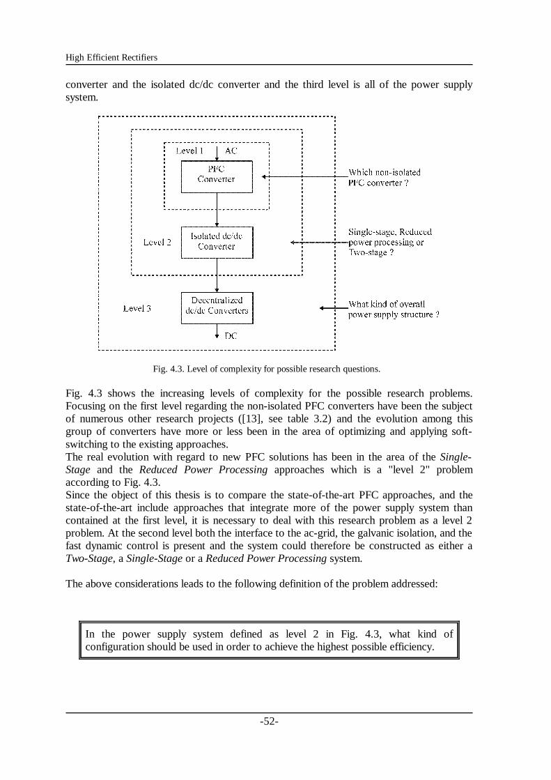
High Efficient Rectifiers
converter and the isolated dc/dc converter and the third level is all of the power supplysystem.
Fig. 4.3. Level of complexity for possible research questions.
Fig. 4.3 shows the increasing levels of complexity for the possible research problems.Focusing on the first level regarding the non-isolated PFC converters have been the subjectof numerous other research projects ([13], see table 3.2) and the evolution among thisgroup of converters have more or less been in the area of optimizing and applying soft-switching to the existing approaches.The real evolution with regard to new PFC solutions has been in the area of the Single-Stage and the Reduced Power Processing approaches which is a "level 2" problemaccording to Fig. 4.3.Since the object of this thesis is to compare the state-of-the-art PFC approaches, and thestate-of-the-art include approaches that integrate more of the power supply system thancontained at the first level, it is necessary to deal with this research problem as a level 2problem. At the second level both the interface to the ac-grid, the galvanic isolation, and thefast dynamic control is present and the system could therefore be constructed as either aTwo-Stage, a Single-Stage or a Reduced Power Processing system.
The above considerations leads to the following definition of the problem addressed:
-52-
In the power supply system defined as level 2 in Fig. 4.3, what kind ofconfiguration should be used in order to achieve the highest possible efficiency.

Problem statement
In the comparison the following basic specifications for the system will be used:
Input current according to EN61000-3-2 (*) Universal input voltage range (90VAC-270VAC) Galvanic isolation Fast control of the dc output voltage
(*) EN61000-3-2 is a European standard and is therefore not directly applicable to otherregions but it is common practice to scale the limits of EN61000-3-2 with the line voltage.The nominal line voltage in Europe is 230VAC whereas is North America the nominalvoltage is 115VAC. The harmonic current limits according to EN61000-3-2 is thereforemultiplied with a factor of 2.
The above specifications are general specifications that can be expected for a modern powersupply system.
4.2 The approach of the future
The next step is to improve and/or develop new approaches based on the knowledgeobtained by working with the problems described in the previous section "4.1.1 The state-of-the-art approaches".Any new approach should of course take advantage of this knowledge and the performanceshould exceed the state-of-the-art.
4.2.1 Efficiency driven research.
The overall goal of this thesis is to increase the efficiency of the total power-supply-systemwith the focus directed towards the implementation of the PFC function in such a way thatcompliance with the limits of EN61000-3-2 are possible. Choosing the efficiency as the main parameter is a deliberate choice. An increase inefficiency translates into reduction of the component stress. Since less heat is generated, anincrease in the power density is possible. The reduced component stress also facilitates theuse of less expensive components cutting down costs. After optimizing the efficiency it is of course possible/necessary to compromise so that costcontra the performance match the application but this process should not be the startingpoint. Using cost as a starting point for the research tend to rule out approaches that in theend might turn out to be superior in performance and cost.
4.2.2 Improving the efficiency
Before thinking about how the efficiency can be improved it is important to determine inwhat way this improvement should manifest. There are several options when includingranged input voltage and fluctuating loads. The efficiency improvement sought in this workis the worst case efficiency determined as the efficiency that limits the converter operation
-53-

High Efficient Rectifiers
by thermal constrains. This usually corresponds to the full-load, low line worst caseefficiency.
The target of the efficiency improvement is illustrated in Fig. 4.4 as the "Before" and"After" curves. The solid line ("Before") represents a typical efficiency curve for a boost-type PFC converter.
Fig. 4.4 The target of the efficiency improvement – increasing the worst case efficiency.
Because of the nature of the losses (described in Chapter 7), the efficiency tends to droprapidly when the input voltage is reaching the low end in the universal line range. The optimal converter would have a high, constant efficiency over the entire voltage range,preferable 100%, but realistically, an efficiency-curve illustrated by the dotted line in Fig.4.4 relative to the solid line would be regarded as a success.The dotted efficiency-curve illustrates a reduced span of efficiencies over the entire linerange. Preferable we would like this efficiency-curve to end the same place at high line asthe before-curve, but a reduction of the high line efficiency is acceptable if it results in animprovement of the worst case efficiency (the one that determines the worst casetemperature rise).The efficiency numbers are realistic but they are not based on any specific circuit. They aremerely put there to illustrate the point about improving the efficiency.
4.2.3 The converter "wish list"
The comparison of the state-of-the-art solutions will be based on the power supply structureand the specifications defined in section 4.2.1. In general, the comparison will not take intoaccount that different topologies offers different features, simply not to complicate mattersfurther. But in any new approach, ideally, we would like to integrate all of the strong sidesof each of the known PFC approaches into a single converter.
The specifications that we would wish for in such a converter, incorporates some of thefollowing features:
Current limiting: Inrush-, output current Independent output voltage (not dependent on the input voltage) Continuous input current
-54-

Problem statement
Low component stress
The inrush current limiting is a general problem for the non-isolated boost-type convertersand for all of the Single-Stage solutions. This is also a problem in the Reduced PowerProcessing approaches where the energy-storage capacitor is located on the AC-side of thegalvanic isolation.For some of the non-isolated PFC converters the choice of output voltage is more or lessgoverned by the input voltage e.g. the boost converter where the output voltage has toexceed the maximum peak input voltage.Continuous input current reduces the input filter requirements dramatically. The requireddamping of the discontinuous input current will be at least an order of magnitude, andincrease for the higher harmonics [14] (section 8.4.5).The low component stress is the first step to improve the efficiency. The thermal layout alsobecomes more simple if the component stress is reduced.
4.3 Summary
The overall problem dealt with in this thesis, is PFC and compliance with EN61000-3-2,with focus on improving the conversion efficiency. In this process a fundamental questionarises. The question is whether the power supply designers should go for one of the state-of-the-art solutions described as the Single-Stage or the Reduced Power Processingapproach or if the designers should use the well proven Two-Stage approach where the PFCfunction is separated and contained in the first stage.In order to compare these approaches it is necessary to set up a framework where acomparison is fair and possible. This comparison only makes sense for a limited choice ofpower supply structures and only if the second-stage converter is included together with thePFC converter. The basic comparison is thereby no longer a comparison of different PFCconverters but a comparison of different power supply systems.
The second part of this thesis is devoted to find a new approach based on knowledgeobtained in the first part. Improving the efficiency is the primary goal but the new approachshould also include good interface capabilities to the utility-line respectively the load. Thecapabilities of any new solution can be summarized by the converter "wish list" presentedearlier:
Current limiting: Inrush-, output current Independent output voltage (not dependent on the input voltage) Continuous input current Low component stress
-55-

High Efficient Rectifiers
Blank page
-56-

Chapter 5
Converter component stress
The amount of literature published in the area of PFC is enormous. By recognizing thedifferent groups/approaches (Chapter 3.) the task of discarding certain topologies becomespossible.
In order to discard certain groups of topologies the criteria used must be consideredthoroughly. A system priority list (cost, efficiency, size....) is often used together withcircuit specifications (voltage-ripple, dynamics...). When using these criteria the choiceusually depends on know-how and “rules of thumb”. These methods are in most cases verygood since they are based on experience, but the choices made can be very difficult toquantify.
It is not likely that one can develop a generic tool that exactly determines which topology tochoose in a given situation. But some of "rules of thumb” adopted through the years can bequantified. This is done in [15] where the basic topologies are compared by investigatingthe component stress in a somewhat generic fashion. This method produces an output (anumber) that indicates the size of the stress on the component, termed Component LoadFactor (CLF). This method of calculating the CLF for the different topologies will be usedas an indication of which topologies possesses the best abilities concerning efficiency.Where a direct comparison between two specific circuits is necessary the specific CLF’s foreach component group can be calculated.
5.1 Introduction to Component Load Factors
The method used to compare the different approaches take its basis in the concept ofComponent Load Factors (CLF) introduced in [15]. Component stress can be translatedinto cost, size and efficiency so investigating the basic topologies and reviewing how thecomponent stress evolves under different circumstances an overview of reasonable solutionsare obtained together with an overview of what not to do. The knowledge obtained fromthe use of CLF can then be used to recognize where unnecessary component-stress is
-57-

High Efficient Rectifiers
produced.
The motivation for using a tool like CLF to compare different converter topologies is that itgives a quantitative measure of the performance of the converter. This is very useful whenchoosing between topologies.
Definition of CLF:
CLF=V *⋅I *
P
(5.1)
P is the total through power of the system and V* and I* are component-dependent voltagesand currents that characterize the stress imposed. In the following, the voltages and currentsthat characterizes the component stress for some of the commonly used power componentswill be listed.
Active and passive switches:
For active and passive switches, V* is defined as the maximum blocking voltage and I* isdefined as the conduction current. The conduction current can be expressed in terms ofpeak-currents, rms-currents and average currents.
For MOSFETs, the product involving peak-currents and rms-currents are of interests. Theswitching losses are sensitive to peak-currents and the conduction losses are sensitive torms-currents.For IGBTs (bipolar-conduction) peak-currents are of interest because of the switchinglosses. Typically the conduction characteristics of the IGBTs are sensitive to average-current so the product involving average-current is of interest.
Rectifiers also have bipolar-conduction characteristics so average-current is used withrespect to conduction losses. If the ratio of IRMS to IAV is large, the rms-currents will alsocontribute significantly to the conduction losses. As for the other switches, the switchinglosses are sensitive to peak-currents.
Transformers:
For transformers, V* is defined as the peak-to-peak winding voltage and I* is defined as thewinding current. The flux density is proportional to the average winding voltage andthereby the core losses. The rms-current is of interest since it affects the winding losses. So,for high-frequency transformers the product of average winding voltage and rms-current isused. The CLF for each winding is calculated and summarized to give the total transformerCLF.
Inductors:
For high-frequency inductors the considerations for the transformers apply. In this context,high frequency means that the inductor size is not limited by core saturation but byhysteresis losses.
-58-

Converter component stress
“Second stage” filter inductors are not subjected to large AC-voltages so the simple V*, I*
product is not useable. If comparison is needed between these inductors, energy calculationscan be carried out.
Capacitors:
For capacitors, the V*, I* product of interest is the maximum capacitor voltage and the rms-current.
In table 5.1, the voltages and currents of interests for each component is summarized.
Components Currents Voltages
MOSFET IPeak, IRMS VPeak
IGBT (bipolar) IPeak, IAverage VPeak
Rectifiers IPeak, IAverage VPeak
Transformers IRMS VAverage
Inductors IRMS VAverage
Capacitors IRMS VPeakTable 5.1. Voltages and currents of interest when calculating CLF
5.2 Using CLF on the basic topologies
To keep the CLF calculations simple, the following assumptions are made:
PIN = POUT
Inductor ripple-current is small – meaning that square current waveforms arebeing switched.
The first assumption simply states that the power losses that would occur in real circuits areneglected. CLF is in it self an indicator of how efficient the power is processed sointroducing the efficiency for each converter would make the CLF calculations obsolete.The second assumption means that the switching currents are square waveforms and theinductor currents are dc-currents. Whether you are assuming infinite or finite inductance, itis still the same volt-seconds that are applied to the inductor so the only difference is therms-value of the current. Since the relative difference between the topologies will be thesame, the "large L" assumption is used to make calculations simple.
5.2.1 Basic non-isolated topologies
The Component Load Factors for the three basic topologies buck, boost and buck-boostwill be presented in the following. Since CLF represents accumulated stress for eachcomponent type, the calculated CLF of the basic buck-boost converter shown in Fig. 5.1cwill actually represent the CLF for all buck-boost derived converters like the SEPIC, Cúk
-59-

High Efficient Rectifiers
etc.
If MOSFETs are used as switches (Q) in Fig. 5.1, the characterizing currents are the peak-,and rms-currents. For the diodes the currents of interests are the peak-, and average-currents and to some extend rms-currents. The inductors (L) in Fig. 5.1 are all high-frequency inductors, so the use of rms-currents and the average voltage will characterize thestress. The capacitors are sensitive to the dc-voltage and the rms-currents.
Fig. 5.1. The 3 basic dc/dc converters. a) Buck dc/dc converter. b) Boost dc/dc converter. c) Buck-boostdc/dc converter.
Example: Calculating CLF
Consider the the boost- and the buck-boost converter in Fig. 5.2. Each converter isoperating with a switch duty-cycle of 50% and operating from the same source voltage withthe same input power.
Fig. 5.2. Converters processing the same input power from the same source-voltage and with the sameswitch duty-cycle (d=0.5). a) Boost. b) Buck-boost.
Each of the two basic converters shown in Fig. 5.2, consists of 5 power components, eachsubjected to a certain amount of stress. To clarify the method, calculations of the CLF ofeach component will be shown in the following.
The switches Q, D:
In this example, peak voltages and peak currents are used to calculate the switch CLF. Inthis case the CLF of active and passive switches are the same.
Boost:
When the switch is on, it carries the inductor current, I. When the switch is off, the voltageacross the switch is determined by the output voltage, which is 2·V.
-60-

Converter component stress
CLFSwitch=2⋅V⋅I
P=
2⋅V⋅IV⋅I
=2(5.2)
Buck-boost:
The inductor current is 2·I, so the switch current is also 2·I. The blocking voltage is 2·V.
CLFSwitch=2⋅V⋅2⋅I
P=
2⋅V⋅2⋅IV⋅I
=4(5.3)
The inductors:
Boost:
For the boost inductor the average voltage applied to the inductor in both the "ON" and"OFF" period is equal d·V.
CLFInductor=2⋅0.5⋅V⋅I
P=
2⋅0.5⋅V⋅IV⋅I
=1(5.4)
Buck-boost:
The applied average voltage is the same as for the boost inductor, but the buck-boostinductor carries twice the current.
CLFInductor=2⋅0.5⋅V⋅2⋅I
P=
2⋅0.5⋅V⋅2⋅IV⋅I
=2(5.5)
The capacitors:
The capacitor CLF will be calculated as the accumulated capacitor stress. The supply-current to the converters and the load current from the converters are considered dccurrents. This means that the CLF of the C1 capacitor for the boost converter in Fig. 5.2a iszero. The buck-boost converter of Fig. 5.2b has discontinuous currents at both the in- andthe output, resulting in non-zero CLF for both C1 and C2.
Boost:
CLFCapacitor=2⋅V⋅0.5⋅I
P=
2⋅V⋅0.5⋅IV⋅I
=1(5.6)
Buck-boost:
CLFCapacitor=(V⋅I )+(V⋅I )
P=
2⋅V⋅IV⋅I
=2(5.7)
The calculated CLF of all the components of Fig. 5.2 are summarized below in Table 5.2
-61-

High Efficient Rectifiers
Converter Transistor Diode Inductor Capacitor
Boost 2 2 1 1
Buck-boost 4 4 2 2
Table 5.2. Calculated Component Load Factors for the 2 converters shown in Fig. 5.2.
In this particular operating point (d=50%), the component stresses are a factor of 2 higherfor buck-boost converter compared to the boost converter. Depending on the point ofoperation, the component stresses will change. In the above example the selected operationpoint was determined by selecting the same switch duty-cycle. It will become evident laterin this section, that this selected operation point, actual is the best case operation point forthe buck-boost derived converters. The optimal operation point for the boost converter iswhen the switch duty-cycle goes towards zero.
The component stress evolves as the input to output ratio changes and this information isvery important to know in order to select the optimal operation point for converters
In order to create and overview of how the component stress evolves as a function of theoutput to input ratio the CLF of each power component for the 3 basic converter topologiesis shown in Fig. 5.3 – 5.7.
The buck converter is only able to step-down the input voltage. This results in an output toinput ratio in the range of ]0;1[. The boost converter is only able to step-up the inputvoltage which results in an output to input ratio in the range of ]1;∞[. The buck-boostconverter is able to both step-down and step-up the input voltage resulting in an output toinput ratio in the range of ]0;∞[.
Fig. 5.3. Transistor CLF calculated with peak voltages and rms-currents
Fig. 5.3 shows the CLF for the active switch using peak voltage and rms-current. Regardingthe conduction losses in the active switches, the rms-currents are the determining factor.The output to input ratio is shown in a logarithmic scale, in order to visualize thecomponent stress in a logical way.The switch stress for the buck converter is shown as the "long-dashed" line. Because of thestep-down characteristics of the buck converter the line ends at an output to input ratio of1. The minimum stress occurs at VOUT/VIN = 1 which corresponds to a duty-cycle of 100%.
-62-

Converter component stress
In terms of CLF, the minimum stress for the buck converter is equal to 1.This is not the case for the switch stress in the boost converter shown as the "short-dashed"line in Fig. 5.3. The minimum switch stress also occurs at VOUT/VIN = 1 but the CLF isequal to zero which corresponds to a duty-cycle of 0%. The buck and the boost converter isclosely related and as shown in Fig. 5.5 the stress characteristics of the passive switch(diode) in the buck and the boost topology, exhibits complementary stress behaviorcompared to the active switches.The switch stress in the buck-boost converter is shown as the the solid line in Fig. 5.3. Ascan be seen, the buck-boost converter generates more switch stress compared to the buckand the boost converters.In the minimum stress situation, both the buck and the boost converters enables a continuesdirect dc path from the input terminals to the output terminals which facilitates the lowcomponent stress. The buck-boost converter is unable to do this since all power obtained atthe input terminals has to be stored in the inductor before the power can be delivered to theoutput terminals. Therefore, the buck and the boost converters are often referred to as"direct" converters and the buck-boost converter as an "indirect" converter.
For the switching losses, the determining factors are the peak voltages and currents. Theswitch CLF using peak voltages and currents are shown in Fig. 5.4.
Fig. 5.4. Transistor CLF calculated with peak voltages and peak currents
In terms of switch CLF using peak voltages and currents, the stress in the buck and theboost converter evolves in a similar way. The CLF is actually proportional to the output toinput ratio for the boost converter and proportional to the input to output ratio of the buckconverter. The minimum CLF for both topologies is equal to 1.The minimum CLF for the buck-boost converter is a factor of 4 higher compared to thebuck and the boost converters.
The diode CLF is shown in Fig. 5.5, where the characterizing current used was the averagecurrent. It is worth noticing, that the diode CLF for the boost converter is constant andindependent of the step-up ratio. As the output voltage increases, the average diode currentdecreases for the same constant output power. The CLF model is purposely very simple anddoes not account for behavioral change of higher voltage rated devices. It is well known,that reverse recovery problems related to the diodes are very much a function of the diodesvoltage-blocking capabilities. Therefore, when using CLF to compare circuits, one shouldbare in mind the limitations of the CLF-model. A CLF comparison will supply the best
-63-

High Efficient Rectifiers
result if the voltage rating of the components are comparable. The CLF of the diode in the buck converter is subjected to a considerable change in stressas the step-down ratio increases. As the input voltage goes up, both the voltage stress andthe average current stress increases.
Fig. 5.5. Diode CLF calculated with peak voltages and average currents
The inductor CLF is shown in Fig. 5.6. As mentioned earlier, the buck-boost topologystores all energy in the inductor before supplying it to the load. The buck and boostconverters also store energy in the inductor, but for these converters the portion of energystored is related to the conversion ratio. The ratio of directly supplied energy to totalsupplied energy, is equal to the output to input voltage ratio for the buck converter and theinput to output voltage ratio for the bost converter.
Fig. 5.6. Inductor CLF calculated with average applied voltages and rms-currents.
The buck and the boost converter has the inductor connected directly to the outputrespectively the input terminals facilitating continuously current flow at one of the terminals.For the buck-boost converter the currents at both the input and output terminals arediscontinuous. This affects the capacitor stress. The capacitor CLF is calculated using theassumption that the source and the load currents are dc-currents. This means that the inputcapacitor in the buck converter, the output capacitor in the boost converter and both theinput and the output capacitor in the buck-boost converter, are subjected to stress.
-64-
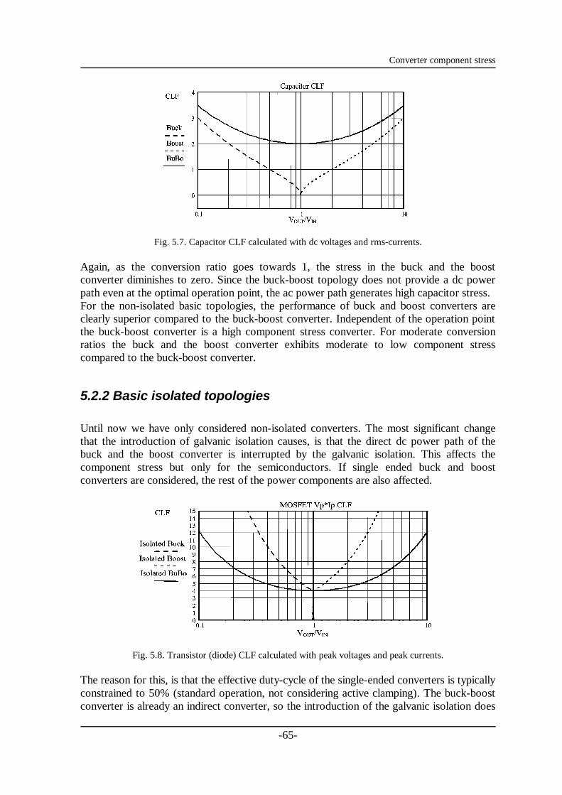
Converter component stress
Fig. 5.7. Capacitor CLF calculated with dc voltages and rms-currents.
Again, as the conversion ratio goes towards 1, the stress in the buck and the boostconverter diminishes to zero. Since the buck-boost topology does not provide a dc powerpath even at the optimal operation point, the ac power path generates high capacitor stress.For the non-isolated basic topologies, the performance of buck and boost converters areclearly superior compared to the buck-boost converter. Independent of the operation pointthe buck-boost converter is a high component stress converter. For moderate conversionratios the buck and the boost converter exhibits moderate to low component stresscompared to the buck-boost converter.
5.2.2 Basic isolated topologies
Until now we have only considered non-isolated converters. The most significant changethat the introduction of galvanic isolation causes, is that the direct dc power path of thebuck and the boost converter is interrupted by the galvanic isolation. This affects thecomponent stress but only for the semiconductors. If single ended buck and boostconverters are considered, the rest of the power components are also affected.
Fig. 5.8. Transistor (diode) CLF calculated with peak voltages and peak currents.
The reason for this, is that the effective duty-cycle of the single-ended converters is typicallyconstrained to 50% (standard operation, not considering active clamping). The buck-boostconverter is already an indirect converter, so the introduction of the galvanic isolation does
-65-

High Efficient Rectifiers
not affect the component stress. Fig. 5.8 and 5.9 shows the semiconductor stress for thebasic isolated topologies.
Fig. 5.9. Transistor CLF calculated with peak voltages and rms-currents.
Isolating the basic buck and boost converter results in a drastic increase in thesemiconductor stress whereas the rest of the components are unaffected by the isolation.Besides the increased semiconductor stress an extra power component is introduced; thetransformer. Compared to the non-isolated buck and boost converters, the semiconductorstress is increased by a factor of 4.Introducing isolation in the buck-boost derived topologies does not affect thesemiconductor stress. Further more, the isolation barrier can be implemented relativelysimple by adding an extra winding on the buck-boost inductor, thereby turning themagnetic structure into a coupled inductor.
5.2.3 Example: Comparing single-ended isolated converters
To demonstrate the effect of isolating the converters (single-ended versions), the CLF ofthe 3 different topologies shown in Fig. 5.10 will be presented. The example uses theForward (Buck-derived), the Flyback and the SEPIC (both Buck-Boost derived).
Fig. 5.10. Single-ended isolated converters with switch duty-cycle d = 0.5. a) Flyback (isolated buck-boostderived). b) SEPIC (isolated buck-boost derived). c) Forward (isolated buck derived).
-66-

Converter component stress
The Forward converter of Fig. 5.10c is used with maximum duty-cycle (d=0.5). In order forinput- and output voltages to be equal, the transformer ratio is set to 1:2. The CLF for the 3converters is listed in table 5.3.
Converter Transistor
Diode Transformer Inductor Capacitor
Forward 4 4 2.8 1 1
Flyback 4 4 2.8 - 2
SEPIC 4 4 2.4 1 2
Table 5.3. CLF for 3 different isolated converters
It may be surprising to see how similar the power-circuits perform. For all 3 topologies, theswitch CLF is the same. For the two buck-boost type converters, the added isolation doesnot affect the semiconductor CLF, but for the Forward converter the increase in CLF,caused by the isolation, is a factor of 4. The Flyback converter has twice the capacitor CLFbut no inductor CLF compared to the Forward converter. The use of single-ended buck orboost derived isolated converters strongly minimizes the differences in component stressseen in the non-isolated versions of the buck, boost and buck-boost type versions.
The boost-derived isolated converters will show similar performance with respect to CLF asthe buck-derived isolated converters. By replacing rectifiers with transistors and vice versain the Forward converter of Fig. 5.10c, the single-ended isolated Boost converter appears.Through all of this section peak-currents and peak-voltages have been used whencalculating switch CLF. One should remember that conduction losses in MOSFETs arerelated to the rms-current, and for bipolar devices, the average-current is the determiningcurrent.
Instead of the single-ended Forward one could use other buck-derived configurations likethe Push-pull or Full-bridge. The total switch CLF does not change but the CLF is spreadout on a larger number of switches. This can be both advantageous and disadvantageous.Besides the larger power handling capabilities, the real advantage of using the bridge or thepush-pull configurations is found when calculating transformer, inductor and capacitorstress. When the effective duty-factor seen by the magnetics and the capacitors canapproach 1 instead of 0.5 the component stress is reduced significantly.
5.2.4 Summarized CLF calculations
One of the strong sides of using a comparison tool like CLF is the simplicity of the method.Supplying the model with the conversion ratio, the component stress is represented by anumber that can be used in the comparison between different topologies.The calculated CLF is summarized in table 5.4.
-67-

High Efficient Rectifiers
Table 5.4. CLF for the basic topologies: buck, boost, buck-boost, isolated buck and isolated boost. **Doesnot apply to single-ended isolated Buck- and Boost converters
5.3 Properties of static and dynamic up/down conversion
The operation point of the different converters is the determining factor of the amount ofstress applied to the power components in the converters. Choosing the right topology andoperation point, can reduce the stress significantly.
5.3.1 Static up/down conversion
In this context, the static conversion is defined as a conversion between a fixed inputvoltage and a fixed output voltage, resulting in a fixed conversion ratio.This is not the predominant situation in real life applications. Usually, the power systemshould be able to handle a specified input voltage variation. Also the demand for hold-upcapability, can be translated into an input voltage variation (in case of buck derivedconverters).In order to demonstrate the properties of a static up/down conversion and the effects on thedifferent topologies the almost unavoidable input voltage variations will be ignored at thispoint.
Consider the power supply system shown in Fig. 5.11.
Fig. 5.11. Power supply system with static conversion ratio.
The system has to the convert the voltage from VIN to x·VIN. Based on the basic topologies,
-68-

Converter component stress
there are 5 different topologies to choose from to solve the problem described in Fig. 5.11.If x>1 (step-up), the following converters can be used: Boost (since x>1) Buck-boost Isolated buck Isolated boost Isolated buck-boost
Even though the power system of Fig. 5.11 need to perform a step-up conversion, theisolated buck derived converters can also be used, since the step-up action can beaccomplished by the transformer turns-ratio. The non-isolated buck and boost convertersare each others complementary circuits, so the observations made in the following is alsovalid for x < 1 (with buck instead of boost).
Staticratio
Topology Switch Diode Inductor Transformer Capacitor
x=2 Boost 2 2 1 - 1
Buck-boost 4.5 4.5 2 - 2.1
Isolated buck or boost 4 4 0 2 0
Isolated buck-boost 4 4 - 2.8 2
x=4 Boost 4 4 1.5 - 1.7
Buck-boost 6.3 6.3 2 - 2.5
Isolated buck or boost 4 4 0 2 0
Isolated buck-boost 4 4 - 2.8 2
x=8 Boost 8 8 1.8 - 2.6
Buck-boost 10.1 10.3 2 - 3.2
Isolated buck or boost 4 4 0 2 0
Isolated buck-boost 4 4 - 2.8 2
Table 5.5. Component stress for 3 different static conversion ratios.
In order to demonstrate the properties of the different topologies, the CLF of the 5converters will be investigated when x=2, x=4 and x=8. The results summarized in table 5.4in the previous section, are used to calculate the component stress shown in table 5.5.
x=2: Given a step-up ratio of 2, the boost topology is clearly the best choice. For theisolated converters, the turns-ratio of the transformer is adjusted in such a way, that theoptimum operation point is achieved. For the isolated buck and boost derived converters,this results in very low inductor and capacitor stress, but it also means an added transformerwith associated component stress. The buck-boost and the isolated buck-boost aresubjected to the largest amount of stress.
x=4: At this step-up ratio, the semiconductor stress are the same for the boost and theisolated boost/buck derived converters. The boost inductor stress is almost at the level ofthe transformer stress in the isolated buck (boost) (high-frequency transformer and inductor
-69-

High Efficient Rectifiers
stresses are comparable), and the capacitor stress, in case of the boost converter, is higherthan for the isolated counter part. The buck-boost family are subjected to the highestcomponent stress.
x=8: Since the turns-ratio of the transformer keeps the operating point of the isolatedconverters at the optimal point, the component stress does not change. At this large step-upratio, the semiconductor stresses of the boost converter are twice that of the isolatedconverters and when comparing the overall component stress the isolated buck (boost)derived converters are superior.The largest component stress is still found in the buck-boost converter.
The observations made on the component stress, in case of a static conversion ratio, resultsin the following key points:
The boost (buck, x<1) converter is subjected to smallest amount of component forconversion ratios up to about 4.
Isolated buck/boost converters should be considered when the conversion ratioapproaches a factor of 4. At higher conversion ratios the isolated buck (boost) derivedconverters are subjected to the smallest amount of stress.
Based on the component stress, the buck-boost derived converters should never be usedfor static conversion.
5.3.2 Dynamic up/down conversion
The situation where the input voltage varies is in this context called dynamic up/downconversion. In the previous section the static up/down conversion has been presented andthe difference between these to cases can be seen comparing Fig. 5.11 and Fig. 5.12.
Fig. 5.12. Power supply system with dynamic conversion ratio.
In this case, where the conversion ratio changes, the component stress for the differenttopologies will not follow the same pattern as discovered in the previous section. Theimpact of the dynamic conversion ratio using V2/V1 = 2, V2/V1 = 4 and V2/V1 = 8 will beexplored in the following. Besides the dynamic conversion ratio, a static conversion ratiocould exist (VOUT ≠ V2 or VOUT ≠ V1), but in this comparison, we will allow VOUT to assumethe value that minimizes the component stress.
The results of calculating the component stress is shown in table 5.6 (worst case).
-70-

Converter component stress
Dynamicratio
Topology Switch Diode Inductor Transformer Capacitor
X=2 Boost/buck 2 2 1 - 1
Buck-boost 4.1 4.1 2 - 2
Isolated buck or boost 8 8 1 2 1
Isolated buck-boost 4.1 4.1 - 2.8 2
X=4 Boost/busk 4 4 1.5 - 1.7
Buck-boost 4.5 4.5 2 - 2.1
Isolated buck or boost 16 16 1.5 2 1.7
Isolated buck-boost 4.5 4.5 - 2.8 2.1
X=8 Boost/buck 8 8 1.75 - 2.64
Buck-boost 5.2 5.2 2 - 2.3
Isolated buck or boost 32 32 1.75 2 2.64
Isolated buck-boost 5.2 5.2 - 2.8 2
Table 5.6. Component stress for 3 different dynamic conversion ratios.
X=2: The boost/buck topology is superior to the rest of the topologies. Even at thismoderate variation of the input, the isolated buck (boost) derived topologies are subjectedto a large increase in semiconductor stress, whereas the rest of the components, aresubjected to the same stress as the non-isolated counterpart.
X=4: The boost/buck topology is still superior but the difference in the component stresscompared to the buck-boost type converters has become smaller.The semiconductor stress of the isolated buck (boost) derived converters increases linearlywith the input voltage variation.
X=8: At this extreme input voltage variation, the buck-boost type converters scores thelowest semiconductor stress, even compared to the boost and the buck topology.
The observations made on the component stress in case of a dynamic conversion ratioresults in the following key points:
Isolated buck and boost derived converters subjected to even a small dynamic conversionvariation results in large semiconductor stress.
The boost- and buck-type converters are superior to other topologies as long as thedynamic conversion ratio is in the area or below a factor of 4.
The buck-boost type converters handles extreme (8 and above) dynamic conversionratios relatively well.
The reason, that the buck-boost type converters handles the extreme voltage variations sowell, can be explained by two things. First of all, the ability to both step-up and step-downfrom the input voltage makes it possible to select an operation point from where theeffective dynamic variation, can be reduced considerable. By selecting the output voltage tohave the same relative distance to the two outer points in the input range, the effectivedynamic range is reduced to:
-71-

High Efficient Rectifiers
K Effective=V IN,high
V IN,low
(5.8)
E.g. the effective input range in case of an 8:1 variation is reduced considerable for thebuck-boost derived converters:
K Effective= 8=2.8 (5.9)
The second feature that helps reduce the stress at extreme variations, is the non-linearcharacteristics of the steady-state transfer function:
GainVout ⁄Vin=d
1d(5.10)
The buck-boost type transfer function has a relatively large gain compared to the boost andbuck type converters. Furthermore, the semiconductor CLF for the buck-boost convertersis not a very precise measure of the stress when the converter is subjected to a dynamicvoltage range, since the CLF calculations does not take into account the degenerativeeffects of using higher voltage rated devices.
5.3.3 Key points
Of all the power components, the semiconductors are the most sensitive components withregard to stress related to which type of converter topology is used and the size of the inputrange. For the magnetic components and the capacitors the stress is in general related to thesize of the input range and not so much the actual converter topology. This makes thesemiconductor-stress a good measure of how efficient the power is being processed. Thisapplies for buck and boost converters and isolated versions of these, but not so much forthe buck-boost derived converters.The buck-boost converters have high overall stress and are not affected by the size of theinput range the same way as the buck and the boost converters are. For moderate inputranges (<4:1) the buck-boost converter produces significantly more component stresscompared to the buck and boost converters but at larger input ranges, this tends to evenout, and at extreme input ranges the buck-boost converter produces the least amount ofstress.
5.4 Using CLF on the basic power conversion systems
The CLF describes the stress of each component class, so comparing different powersystems using CLF, will result in a comparison of each of the component groups. Whichsystem offers the lowest total stress and thereby resulting in the highest possible efficiency,will be a matter of a subjective assessment. If all component stresses are lower in one of thepower systems, this assessment is very easy but otherwise it can be quite difficult.
-72-

Converter component stress
5.4.1 Single-stage vs. two-stage, a simple comparison
The requirements of the power system often include galvanic isolation. Therefore, anisolated converter has to be included in the power system.
Fig. 5.13. Simple power system configurations. a) Single-Stage system. b) Two-Stage system.
Consider the two power systems shown in Fig. 5.13 which represents a Single-Stage systemand a Two-Stage system. Since galvanic isolation is almost always a demand, staticconversion ratios can be taken care of by the transformer turns ratio without any increase incomponent stress. If there is no dynamic variation at the input, the optimal choice withregard to minimum overall component stress is a Single-Stage solution using a buck or aboost derived isolated converter (based on the calculations of table 5.5). For a dynamic input range of a factor 4, the isolated buck or boost derived convertersshould be used in the Two-Stage configuration, simply because of the excessive increase insemiconductor stress whereas the buck-boost derived isolated converters could be used in aSingle-Stage system since the component stress in these types of converters is relativelyimmune to the voltage variations.Table 5.7 summarizes the CLF of a Single-Stage system using an isolated buck-boost typeconverter compared to a Two-Stage system using buck and/or boost derived converters. Forthe Two-Stage system the voltage variation is handled by the non-isolated converter.
Component Single-stage
Isolated buck-boost
Two-stage
Total Non-isolated boost Isolated buck
Switches 4.5 8 4 4
Diodes 4.5 8 4 4
Inductors - 1.5 1.5 0
Transformers 2.8 2 - 2
Capacitors 2.1 1.7 1.7 0
Table 5.7. Power system comparison between a single-stage and a Two-Stage system for a 4:1 dynamicinput range.
The most significant difference in CLF occurs with regard to the semiconductors. As shownearlier, the minimum CLF of a buck-boost type converter is 4, so the increase in CLF when
-73-

High Efficient Rectifiers
subjected to 4:1 dynamic range is only 0.5! As mentioned earlier, the CLF for the switchesin the buck-boost type converters is not a very precise measure when it comes to voltagevariations. The influence of the higher voltage rating of the semiconductor devices will betaken into account in an example in chapter 6. The Two-Stage system have a total semiconductor stress of 8 which is almost twice that ofthe Single-Stage buck-boost converter. One could also choose to use an isolated buck orboost type converter in a Single-Stage system but the semiconductor stress will increasewith a factor of 4 in the isolated converter resulting in a total increase in the semiconductorstress of a factor of 2.
5.4.2 Key observations
Potentially, the buck-boost type converters are a reasonable choice for a wide input rangeconverter. The initial stress is high in these converters, but the ranged input seems to havelittle effect on the component stress. The isolated buck converter, is without a doubt the predominant isolated dc/dc converterfor high performance systems. In case of moderate to large input range, the isolated buckconverter should be used in a Two-Stage system in order to lower the semiconductor stress.Another important observation is, that increasing the number of stages does not impact theCLF of the inductors and the capacitors as long as buck and/or boost derived converters areused. Given a dynamic input range this will result in a predetermined inductor and capacitorstress regardless of the number of stages being used.
5.5 The relation between dc- and ac-CLF
Until now, all comparisons and stress calculations have been carried out on basic dc/dcconverters. In order to use the observations made in this process, a correlation between thedc/dc and the rectified ac/dc case has to be established.
5.5.1 Ac-CLF
Developing an ac/dc-version of the Component Load Factor is not as straight forward asfor the dc/dc version. The good thing about CLF for the dc/dc converters is the simplicity ofthe method. This also insures that the correlation between the calculated stress factors andthe actual component stress is not lost in the process. For the ac/dc converters, thecomponent voltages and/or currents change during the line period. Therefore, some kind ofaveraging is needed to obtain a simple number that describes the stress. Doing so, some ofthe characteristics of the circuit may disappear in the process together with the usefulness ofthe method. In the ac/dc case, the inductors carry both a low and a high frequency component, both timevarying, which makes it unsuitable to be characterized with a simple number as done in thedc/dc case.Semiconductor stress can to some extend be characterized using the same methods as in theprevious section. An example of the computed switch stress for 3 obvious PFC candidates
-74-
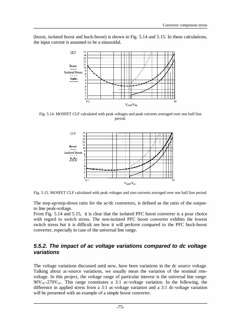
Converter component stress
(boost, isolated boost and buck-boost) is shown in Fig. 5.14 and 5.15. In these calculations,the input current is assumed to be a sinusoidal.
Fig. 5.14. MOSFET CLF calculated with peak voltages and peak currents averaged over one half lineperiod.
Fig. 5.15. MOSFET CLF calculated with peak voltages and rms-currents averaged over one half line period.
The step-up/step-down ratio for the ac/dc converters, is defined as the ratio of the output-to line peak-voltage.From Fig. 5.14 and 5.15, it is clear that the isolated PFC boost converter is a pour choicewith regard to switch stress. The non-isolated PFC boost converter exhibits the lowestswitch stress but it is difficult see how it will perform compared to the PFC buck-boostconverter, especially in case of the universal line range.
5.5.2. The impact of ac voltage variations compared to dc voltagevariations
The voltage variations discussed until now, have been variations in the dc source voltage.Talking about ac-source variations, we usually mean the variation of the nominal rms-voltage. In this project, the voltage range of particular interest is the universal line range:90VAC-270VAC. This range constitutes a 3:1 ac-voltage variation. In the following, thedifference in applied stress from a 3:1 ac-voltage variation and a 3:1 dc-voltage variationwill be presented with an example of a simple boost converter.
-75-

High Efficient Rectifiers
Example: Effects of ac and dc voltage variations on the stress applied to the switch.
In this comparison, the ac/dc and dc/dc boost converter step-up the input voltage to thesame output voltage, which is set to the the maximum occurring input voltage. The outputpower is the same for both converters.
Ac-input: 90 VAC – 270 VAC, sinusoidal current waveform. Dc-input: 127 VDC – 381 VDC, dc current. Dc-output: 381VDC
Applying CLF to an ac/dc converter and comparing it to the CLF of the dc/dc converter,only makes sense if the characteristic voltages and currents that make up the CLF, arecompatible. Rms-currents in both the ac/dc and the dc/dc case are compatible, since themere measure of rms, takes into account variations that will affect the conduction losses. Incase of the boost converter, the output voltage can also be used since it is constant and thesame for both the ac/dc and dc/dc converter in this example. Based on the characteristicvoltages and currents that can be used in this example without destroying the basic idea ofCLF, we can determine on which components of both the ac/dc and the dc/dc converter, theCLF measure would be appropriate to use. These are listed below.
Switch: rms-current and blocking voltage (output voltage) Diode: rms-current and blocking voltage (output voltage) Output capacitor: rms-current and blocking voltage (output voltage)
For the inductor the CLF measure is not a good indicator of stress in case of the ac/dcconverter. The average voltage is fluctuating and the ac/dc inductor has a low frequencycurrent component, which is relative large compared to the high frequency currentcomponent. A way to improve the inductor CLF would be to calculate the applied inductorvoltage as rms. This would account for the fluctuating applied inductor voltages, and thequadratic behavior of the associated inductor core losses. The low frequency currentcomponent is still not accounted for, so to use even this modified CLF version to comparethe inductors, might not be a reasonable measure.
The worst case (largest step-up) CLF of the switch, diode and output capacitor for theac/dc- dc/dc boost converter is shown in table 5.8.
Switch Diode Capacitor
Ac/dc boost 3.6 2.3 2
Dc/dc boost 2.2 1.7 1.4
Table 5.8. Comparison of an ac/dc- and dc/dc boost converter
The ac/dc boost converter is subjected to higher stress compared to the dc/dc version. Thisis not a surprise because of the way that the voltage range for the two cases is defined. Theac/dc boost converter operates with a larger step-up ratio compared to the dc/dc versionexcept at the peak of the ac voltage. Further more, the currents are pulsating, which resultsin higher rms-currents.
-76-

Converter component stress
Another way of comparing these two approaches, is to calculate what dc/dc voltage rangeis equivalent to the ac/dc voltage range, in terms of characteristic currents e.g. switch rms-currents.
Keeping the ac/dc voltage range and adjusting the dc/dc voltage range to equalize the CLFof each component of table 5.8, results in the equivalent voltage ranges shown in table 5.9.
Switch Diode Capacitor
Ac/dc range(3:1)
90VAC-270VAC 90VAC-270VAC 90VAC-270VAC
Dc/dc range 92VDC-381VDC 72VDC-381VDC 76VDC-381VDC
Dc/dc ratio 4.1 5.3 5
Table 5.9. The resulting dc/dc range after equalizing the individual component stress.
A 3:1 voltage range for the ac/dc converters translates into a larger voltage range for thedc/dc converters, typically in the range of 4-5:1.
The key point is, that the ac voltage variations results in higher component stress comparedto the dc voltage variations and that this should be considered in the structure of the powersupply system.
5.6 The pitfalls of CLF
As with any theoretical investigation, the method used, can also be misused to arrive atconclusions that when subjected to real life designs, does not live up to the claimedperformance.
The two most significant properties that the CLF measure does not account for is:
1) The voltage rating of the semiconductors2) Eddy-current losses associated with the magnetics (inductor- and transformer-design)
The most predominant switch in high-frequency converters up to voltage ratings of about600V, is the MOSFET. The on-resistance and the switching capabilities of the MOSFET ishighly dependent on the actual voltage rating (as for any switch-devices). So, for the CLFmeasure to be fair when comparing the semiconductor stress, these should have the samevoltage rating.
Eddy-current losses, particular with regard to transformers and coupled inductors, are nottaken into account. For transformers in buck- and boost derived topologies, the effectiveincrease in the winding resistance, caused by the eddy-currents, can be reduced dramaticallyby interleaving schemes and by using Litz wire. For the buck-boost derived converters usingcoupled inductors to utilize the isolation, interleaving does not reduce the eddy-currentlosses. The only possible way to push the current through the converter is extensive use ofLitz wire. This reduces the copper fill factor which results in increased losses.
-77-

High Efficient Rectifiers
5.7 Summary
Using CLF to characterize the basic topologies have revealed some basic properties that arevery useful to take into account when designing the structure of the power system. TheCLF measure is very simple to apply to dc/dc converters but not practical for ac/dcconverters. None the less, the characteristics of the dc/dc converter stress, can be used as afirst approximation of the performance of the ac/dc converters. As shown in this chapter,the stress applied to the ac/dc converters in case of input voltage variations, translates intostress for the dc/dc converters, that would occur at larger voltage variations.
The inductor and capacitor stress for buck and boost derived converters is closely related tothe size of the input range but not to the number of stages or whether the converter isisolated.A direct comparisons of a power system consisting of both "ac/dc" and "dc/dc" inductorsneeds to take its basis in the actual physical implementation. The inductor stress is thereforenot a very useful (simple) indicator of the power systems performance.
In case of the non-isolated topologies, it is clear that the buck and boost topologies aresuperior to the buck-boost topology. Isolating the buck-boost converters, does not affectthe component stress and compared to isolated buck and boost converters thesemiconductor stress in the buck-boost derived converters is actually lower according toCLF. This might not be the case in a real design, since CLF does not account for differencesin semiconductor voltage ratings.
The examples in this chapter have shown that the semiconductors are the most sensitivecomponents with regard to choice of topology. Furthermore, the semiconductor stress inac/dc and dc/dc converters are without modifications comparable making it a good indicatorof the performance of the power system.
-78-

Chapter 6
Comparing the state-of-the-art approaches
In the previous chapter the basic topologies were reviewed using CLF as a measure of theperformance. The converters perform differently when exposed to voltage variations orwhen galvanic isolation is introduced.In this chapter, these characteristics will be used to identify were excessive componentstress is produced in the state-of-the-art approaches, and compare it with the standard Two-Stage approach. The structure of the power system can also be optimized using CLF, but asshown in the previous chapter, one should sometimes be careful using this method since allimportant information is not included in the CLF.In this chapter the results obtained in chapter 5 will be used on the PFC approachespresented in Chapter 3.
6.1 Typical loss distribution in a universal input PFC boostconverter
In the Two-Stage configuration which will be used in the comparisons against the state-of-the-art approaches, the first stage will be comprised by the PFC boost converter. The PFCboost converter is recognized as one of the most efficient non-isolated PFC converters (ifnot the most efficient). The research in the area of PFC has not produced many newalternatives to the non-isolated PFC boost converter but a significant contribution has beenpresented in [16]. The approach in [16] will be presented in chapter 7.
The worst case losses for the PFC boost converter occurs at low line. For the universal linerange defined as 90-270 VAC, the worst case losses will be at 90VAC. A typical lossdistribution of a PFC boost converter is shown in Fig. 6.1 [17](VAC= 90V, VOUT= 414V,POUT= 1kW).The efficiency at full load and low line for this typical boost converter is about 91%. At highline, 220VAC the efficiency is 96.6%. As shown in Fig. 6.1 chart 2, the MOSFET losses is byfar the largest contributor to the power loss. The output diode losses are relatively low, butthe dynamics of this diode has a significant effect on the MOSFET in terms of increasedswitching losses caused by the diode's reverse recovery. Using fast diodes reduces the
-79-

High Efficient Rectifiers
reverse recovery effect.
Fig. 6.1. Typical distribution of power losses in a PFC boost converter [17].
The boost inductor losses are at low line mainly conduction losses. To reduce these losses asmaller inductance value can be used at the cost of more ripple current which will increasethe filter requirements, produce more conduction losses in the surrounding components andincrease the inductor losses at high line.The input rectifier losses are mainly governed by the rectifiers threshold voltage and theaverage input current. For the boost converter as well as the state-of-the-art approaches thebridge rectifier can be omitted by changing the converter configuration. Typically about halfof the rectifier losses will be transferred to the active switch (MOSFET).The filter losses are tightly connected to the size of the boost inductance and to the powersystem design (common mode noise). Soft-switching techniques can be applied to reducethe filter requirements.
By proper design and optimization some improvements of the converter efficiency can beexpected, but the most significant factor with regard to the efficiency is the switch stress.This, together with the fact that the component stress on all other power components,except the semiconductors, is shifted between the two stages independent of the isolationbarrier, suggests that the measure of how efficient the power conversion system is, can bebased on the semiconductor stress, in particular the active switches (MOSFETs).
6.2 Discussion of the comparisons conducted
The focus in all of the comparisons carried out will mainly be on the losses in the activeswitches. There are several reasons for this.
First of all, the analysis using CLF in chapter 5 showed that the component stress for thecapacitors and the inductors are affected by the voltage variations but not by whether thetopology is isolated or not. Therefore, for a given input voltage variation, the accumulatedstress on the capacitors and the inductors will be more or less the same, whether the voltagevariation is handled by the input-section or the output section. This is generally true whenusing the same types of converters. In all cases, the direct converters represented by thebuck and boost converters generates less stress on the capacitors and the inductorscompared to the indirect converters represented by the buck-boost derived converters.
-80-
Filter 13,00%
Rectifiers 19,00%
Inductor 17,00%
MOSFET 43,00%
Diode 8,00%
Filter Rectifiers Inductor MOSFET Diode
0
0,5
1
1,5
2
2,5
3
3,5
4%
loss
Chart #1 Chart #2

Comparing the state-of-the-art approaches
As shown in chapter 5, the semiconductors in some topologies are greatly affected by theisolation. This means that extra stress in the isolated converter should be avoided andmoved to the non-isolated converter.
Secondly, the goal is to determine the ability to achieve high efficiency. By examining theloss distribution in a PFC boost converter Fig. (6.1), one will find that a significant part ofthe losses are generated in the semiconductors and particularly in the active switch, theMOSFET. For any of the alternative approaches to the Two-Stage configuration, improvedefficiency would basically mean that the semiconductor stress has to be reduced.
6.3 Applied CLF and alternative Stress measures.
CLF can be used directly on dc/dc stages within the power system and give a quantitativemeasure of the performance. For the ac/dc part of the power system, the use of CLF is notan exact measure. Therefore, there is a need to introduce an alternative stress indicator toevaluate the transition from ac to dc in the power system.
One of the key points discovered in chapter 5 was, that isolated converters expose thesemiconductor devices to a great deal of stress especially in case of voltage variations. Onthe other hand, besides the increased semiconductor stress, the rest of the components arenot affected by the isolation.
The alternative stress measure should therefore be able to quantify the stress on thesemiconductors, especially the active switches.
As stated earlier, the most predominant switch in high-frequency converters up to voltageratings of about 600V is the MOSFET. The losses in the MOSFET can be split up into 2types: conduction- and switching-losses. The conduction losses are related to the RDS,ON ofthe MOSFET which again can be related to the physical size of the MOSFET through [23]:
RDS,ON ∝V BR
2,5
ADie
(6.1)
Eq.(6.1) simply states that ideally, the RDS,ON of a MOSFET is proportional to the break-down voltage in the power of 2,5. If the same chip die area (Adie) is used to manufacture a200V and a 400V MOSFET, the RDS,ON of the 400V device would be 5.7 times largerthan for the 200V device.
Eq.(6.1) is still valid for the majority of the products on the market, but new MOSFETtechnologies are changing the limitations of Eq.(6.1).Devices like the CoolMOS from Infineon [18] are using a MOSFET-technology that ideallydoes not obey the more than square proportionality between the RDS,ON and the break-downvoltage [19]. The progress in MOSFET technology will push the relation between theRDS,ON and the break-down voltage towards:
-81-

High Efficient Rectifiers
R DS,ON ∝V BR
2
ADie
(6.2)
The correlation between the switching losses and the chip die area is relatively simple. Thedie area consists of many individual cells in parallel. If a lower on-resistance is required,more cells will be added in parallel. The switching losses are determined by voltages andcurrents being switched and the speed of which we can turn the device on and off.Assuming that standard MOSFET drivers are used, the switching speed of the devices isbasically proportional to the parasitic capacitances [20].
The switching losses can therefore be assumed to be proportional to the switching voltage,switching current and the chip die area.
These relations between the physical size and the performance of the MOSFET will be usedin the following comparisons together with the general concept of CLF.
The relations above will be used, to give a quantitative measure of how efficient the poweris processed by assuming that the same total chip die area is available for each of the unitsbeing tested.
Fig. 6.2. Two different realizations of a 4:1 step-up system. a) Two cascaded boost converters. b) A single-switch version of the converter in a).
To illustrate how the physical behavior described by Eq.(6.2) can be used to quantify thestress, consider the two converters of Fig. 6.2.The converter in Fig. 6.2a is a cascaded boost, where each stage step-up the voltage 2 timesto reach the total voltage step-up of a factor 4. In Fig. 6.2b a single-switch version of theconverter in Fig. 6.2a has been implemented, also stepping-up the voltage 4 times. The two converters are very simple and straight-forward so the difference in switch stresscan easily be shown by using CLF. Using peak- voltages and currents, the CLF=2 for eachswitch in Fig. 6.2a giving a total switch CLF of 4. For the converter in Fig. 6.2b, the switch
-82-

Comparing the state-of-the-art approaches
CLF amounts to 6.So, by using CLF we have a strong indication that the configuration in Fig. 6.2a expose theswitches to less stress than the configuration of Fig. 6.2b.
In case of more complex systems, applying CLF might not be feasible. In these cases the"die area" considerations are useful.
Example:For the converters of Fig. 6.2 we are using the same total chip die area. Intuitively we splitthe die area equally between the two switches in Fig. 6.2a. The conduction losses will thenbe proportional to:
PCon,2stage∝(2⋅V )2
ADie ⁄2⋅I 2⋅D+
(4⋅V )2
ADie ⁄2⋅( I ⁄2)2
⋅D=8⋅V 2
⋅I 2
ADie
(6.3)
For the converter of Fig. 6.2b, the conduction losses will be proportional to:
PCon,1stage∝(4⋅V )2
ADie
⋅(3⋅I2)
2
⋅D=18⋅V 2
⋅I 2
ADie
(6.4)
The conduction losses of the single-switch version of Fig. 6.2b will be exposed to anincrease in the conduction losses of a 125% compared to the configuration of Fig. 6.2a!
Remembering the state-of-the-art solutions classified as "Switch-sharing Single-Stagesystems" in chapter 3, the above example clearly illustrates one of the reasons why thisapproach is a poor choice.
In the above example, the die area was split equally between the two MOSFET devices, butthis is not necessarily the optimal choice. We can define the conduction losses of a "Two-Stage" solution utilizing a total die area equal to ADie as:
PCon,2stage∝C1
1(1x)⋅ADie
+C2
1x⋅ADie
(6.5)
, where C1 and C2 are constants including the voltage rating and rms-currents and x is theportion of die area allocated to one of the two stages.
The optimal choice of x can be found by differentiating Eq.(6.5) and finding the minima ofthis function. Depending on the constants C1 and C2, an optimal choice of x is given by:
x[C2≠C1]=2⋅C2± 4⋅C2
24⋅(C2C1)⋅C2
2⋅(C2C1)
(6.6a)
x[C1=C2]=0.5 (6.6b)
There are two solutions to Eq.(6.6a), but the right solution gives an x-value in the range of]0;1[.
-83-

High Efficient Rectifiers
In the example we chose x = 0.5, and as it turns out, this is also the optimal choice sinceC1=C2 in Eq. (6.3).
6.4 Comparisons
Even though the results of chapter 5 strongly indicates, that the better approach with regardto component stress is the Two-Stage approach, taking the specifications defined in chapter4 into account, it would be wrong to claim that this is always the case.This section is dedicated to show examples of the more successful Reduced PowerProcessing and Single-Stage schemes and compare these with a Two-Stage solutioncomprised by a boost PFC converter cascaded by an isolated buck-derived converter. Sinceit is not possible in a generic fashion to show that one approach is better than the other, theconclusions obtained are based on comparisons.Some of the comparisons carried out might seem academic and difficult to relate topractical implementations, but none the less, the comparisons are carried out to show thedifferences in how efficient the power is processed.
6.4.1 Reduced power processing vs. Two-stage solutions
The Reduced Power Processing schemes suffers from at least one and usually twostructural/topological problems. First of all, if sinusoidal input current is drawn the ReducedPower Processing scheme always uses an isolated PFC converter directly connectedbetween the ac-grid and the output terminals. This converter is therefore subjected to thefull line variation. Secondly, the auxiliary converter which operates with reduced powerprocessing, is typically implemented with a buck-boost derived converter. The buck-boostderived converters are high component stress converters as shown previously.
6.4.1.1 Auxiliary converter considerations
The Reduced Power Processing approach shown in Fig. 6.3a, follows the principlesdiscussed in section 3.3.2 Reduced Power Processing systems.
Fig. 6.3. Flyback PFC converter with post-regulator. a) Reduced Power Processing scheme [21]. b) Buckpost-regulator.
The PFC converter in Fig. 6.3a transfers the total input power into the series connection of
-84-

Comparing the state-of-the-art approaches
C2 and C1. The auxiliary converter can be identified as Q2, D2 and L2, and this convertertransfers energy from C2 to the output (C1). The best case operation of this circuit is whenthe VAUX = VOUT which results in maximum direct power transfer (50%).In steady state operation, the buck-boost auxiliary converter operates with a duty-cycle of50%, which according to the CLF measure is the optimal operation point. One of theexamples in chapter 5 showed how the buck-boost type converters, even at the optimaloperation point, has twice the CLF score compared to buck and boost converters operatingwith a step-up/down ratio of 2.Keeping the output voltage of the flyback PFC at two times VOUT, a buck converter couldbe implemented with the same components (same voltage rating) as the ones used for thebuck-boost auxiliary converter. The flyback PFC converter cascaded by the buck converteris shown in Fig. 6.3b.Keeping CLF in mind the circuits should perform more or less the same with regard tocomponent stress. The buck-boost auxiliary converter process half the input power but hastwice the component stress of the buck converter which process the full input power.But since the buck converter processes a more or less constant power and the buck-boostconverter process a pulsating power (from zero to full output power), the current stress inthe examples are not the same. Table 6.1 summarizes the differences.
I. Buck-boostpost regulator
II. Buck postregulator
I./II. Ratio
Q2
VPeak 2·VO 2·VO 1
IRMS PO/VO PO/(VO·1.41) 1.41
IP,mean (4·PO)/(π·VO) PO/VO 1.27
D2
VPeak 2·VO 2·VO 1
IAV PO/(VO·2) PO/(VO·2) 1
IP,mean (4·PO)/(π·VO) PO/VO 1.27
L2 VMean VO VO 1
IRMS 1.41·PO/VO PO/VO 1.41
Table 6.1 Comparison of component stress for the two implementations shown in Fig. 6.3.
The pulsating power in the buck-boost converter increases the rms-currents considerableleading to twice the conduction losses in the switch and the inductor compared with thebuck-solution.
The above comparison is a "text-book"-example of the fact, that Reduced PowerProcessing in its self is not the determining factor of how efficient the conversion frominput to output is.
6.4.1.2 Main converter considerations
The fact that an isolated PFC converter has to be used, as the main converter automaticallysets off the alarm bells since isolated converters together with input voltage variations doesnot go well together.
-85-

High Efficient Rectifiers
Fig. 6.4. Comparison of an isolated PFC and a Two-Stage solution. a) Isolated flyback PFC. b) Two-Stagesolution with a boost PFC and an isolated buck-derived dc/dc converter.
To illustrate the performance of the isolated PFC converters a comparison between anisolated PFC converter and a Two-Stage system will be carried out. The isolated PFCconverter is of the buck-boost type (Fig. 6.4a), since these converters seems to be superiorwith regard to semiconductor stress compared to the isolated boost PFC.
The two configurations will be compared using the conditions supplied in table 6.2.
Flyback (Fig. 6.4a) Two-stage (Fig. 6.4b)
VIN 90-270 VAC 90-270 VAC
VOUT,PFC 220VDC* 382VDC
Power P P
PFC IQ,RMS 13.6m·P 9.4m·P
Dc/dc IQ,RMS - 1.85m·P
VBR (Ideal) 602V 382V
Table 6.2. Comparison conditions and results (* minimum stress according to CLF).
The expressions for calculating the switch rms-currents for the PFC flyback and the PFCboost can be found in [5, p.677].
Assuming that the same total chip die area is available for each of the two implementations,the switch conduction losses will be compared using the relations between RDS,ON, break-down voltage and chip die area given by Eq. (6.2). The switch conduction losses in the PFCflyback are proportional to:
PFlyback ∝(V BR,Flyback )
2
ADie
⋅I Q,rms2
(6.7)
For the Two-Stage configuration, the switch conduction losses are proportional to:
P2stage∝(V BR,2ST.)
2
(1x)⋅ADie
⋅I Q,rms,pfc2
+4⋅(V BR,2ST.)
2
(x⁄4)⋅ADie
⋅I Q,rms,dcdc2
(6.8)
The first part of Eq. (6.8) describes the conduction losses associated with the PFC boost.The die area allocated for this stage is expressed by (1-x). The second part describes theconduction losses of the dc-dc stage configured as a full-bridge buck converter. The diearea allocated for all of the switches in the dc-dc stage is equal to x. Therefore, there is only
-86-

Comparing the state-of-the-art approaches
x/4 of die area per switch and since the rms-current flows in all 4 switches, the numerator ismultiplied with 4.
Using Eq. (6.6) to solve for optimum x results in an x = 0.44 which means that 56% of thedie area is utilized for the PFC boost and 44% for the full-bridge dc/dc converter.
Using the values of table 6.2 in Eq. (6.7) and Eq. (6.8), the conduction loss ratio of theactive switches in the two cases can be found:
PFlyback
P2stage
=1.63(6.9)
Even though the same total chip area is utilized in the two configurations, the PFC flybacksolution increases the switch conduction losses with 63%. A part of this increase is causedby the fact that you need higher voltage rated devices.From the investigations of the switch CLF on PFC converters in chapter 5, the findingsstrongly indicated that the isolated PFC boost was a very poor choice. For the completenessof this comparison of isolated PFC converters and Two-Stage systems, the relativeconduction losses of the isolated PFC boost converter will also be calculated.
Fig. 6.5. Isolated PFC boost
The isolated PFC boost of Fig. 6.5 is implemented with a full-bridge. The specifications forthe PFC boost, as part of the Two-Stage system, shown in table 6.2, is also used for theisolated PFC boost. This means, that the reflected output voltage on the primary side isequal to the maximum line peak voltage (382V).
PIso.boost∝4⋅(V BR)
2
(ADie ⁄4)⋅I Q,rms,iso.boost
2 , I Q,rms,iso.boost=6.3m⋅P(6.10)
The switch conduction loss ratio of the isolated PFC boost compared to the Two-Stageapproach, can then be calculated:
PIso.boost
P2stage
=2.34(6.11)
The results of Eq. (6.11) verifies that the isolated PFC boost is a poor choice. Theconduction losses are 134% higher in the isolated PFC boost compared to the Two-Stageapproach!
Until now it has only been the stress on the active switches that has been considered. To
-87-

High Efficient Rectifiers
finish the semiconductor devices, the diodes will briefly be discussed.
The power losses associated with the diodes in PFC applications can be severe. It is not somuch the actual power loss internally in the diode caused by the diode voltage drop and thecurrent, but more some of the diodes parasitic effects that influences the switchingperformance of the active switch. For the p-n diodes, the problem is the reverse recoverycurrent, which the active switch has to deal with during turn-on. This additional current cancontribute considerable to the switching losses.The diode losses becomes a larger part of the total loss budget, as the output voltagedecreases. The advantage of using a Two-Stage system, is that the second stage that has tointerface to the load, operates from a fixed voltage, which means minimum stress on thediodes. If the output is a low voltage type output, the performance of the diodes will be thedetermining factor regarding the efficiency.
For the inductors and the capacitors, the stress follows the topology and/or the voltagevariation and not whether the converter is isolated or not. For the Two-Stage approach, thevoltage variation is handled by the PFC boost converter. Since the isolated dc/dc converteris of the buck type, the stress associated with the inductor and capacitors will be very small,ideally zero, since there is no voltage variations. The flyback PFC is a buck-boost typeconverter which means that the stress imposed on the inductor (coupled inductor) and thecapacitors will be higher than for the PFC boost. The inductor and capacitor stress of the isolated- and the non-isolated PFC boost is thesame since the component stress is not affected by the isolation.
6.4.1.3 Non-sinusoidal reduced power processing
The non-sinusoidal Reduced Power Processing scheme have not been dealt with until now,simply because they are not very common. Typically, when using two separate converterswith separate control, sinusoidal input current is one of the goals.The non-sinusoidal input current shapers are typically classified as Single-Stage converterseven though some of these configurations also have Reduced Power Processing.
The example of a non-sinusoidal Reduced Power Processing scheme is shown in Fig. 6.6a.This scheme has recently been published [22].
Fig. 6.6. a) Flyback input current shaper with Reduced Power Processing [22]. b) Buck input current shaper.
The scheme shown in Fig. 6.6a is comprised by a flyback (isolated buck-boost) where theprimary side winding and switch is placed in series with the capacitor C1. Since some of theinput-current is transferred directly to the input for the next stage, the authors of thisproposed scheme claim it to have Reduced Power Processing. In this case the following
-88-

Comparing the state-of-the-art approaches
converter is a dc/ac converter that drives a fluorescent lamp.
Since the primary side of the flyback converter is in series with the output capacitor, theflyback transfer function is reduced to a step-down function. So, as long as the time varyinginput voltage is below the output voltage of the flyback converter, no input current can bedrained. The flyback converter is operated in DCM.Basically, the flyback converter has obtained the characteristics of a simple buck converter,shown in Fig. 6.6b, with regard to the interface to the ac-grid. When comparing the twoconfigurations of Fig. 6, similar performance will be obtained. A simple comparison hasbeen carried out and the results are shown in table 6.3.The performance of the DCM flyback and the DCM buck converter is very similar. Themost significant difference is that the inductor in the flyback implementation is a coupledinductor with two windings where only one winding is active at the time. The utilization ofthe magnetic component is therefore considerable lower compared to the buckimplementation.
DCM flyback DCM buck DCM boost
VIN / [VRMS] 230 230 230
VOUT / [VDC] 138 138 400
P / [W] 40 40 40
Duty cycle 0.5 0.4 0.19
L / [mH] 3.15 2 3.45
VDS / [V] 384 325 400
IPeak / [A] 1.2 1.5 0.71
IQ / [ARMS] 0.3 0.33 0.11
Table 6.3. Comparison of DCM flyback [22], buck and boost input current shapers.
Even though the flyback converter only process about 50% of the power (compared to aflyback in a normal setup) the buck converter perform similar but process the "full" amountof power.This example demonstrates that all converter topologies are not created equal when itcomes to component stress! The non-isolated buck and boost converters could just as wellbe termed Reduced Power Processing converters.
For the buck converter, the ratio of direct power transfer is equal to the output to inputratio. This supports the findings of chapter 5, where an increase in the step-down ratiocorresponds to an increase in component stress but a decrease in direct power transfer. Thebuck-boost derived converters only uses indirect power transfer which support the highcomponent stress findings.
The first two columns in table 6.3 lists the comparison of the flyback and the buckconfiguration. The third column gives the detail of a DCM boost converter for the sameapplication. The only thing that makes the comparison a little difficult is the difference inoutput voltage. For the boost converter to work, the output voltage has to larger than theline peak voltage (325V) and since the converter is operated in DCM with a constant duty-cycle, the output voltage has to be somewhat larger than the line peak voltage to be able to
-89-

High Efficient Rectifiers
comply with regulations (VOUT = 400V). For the flyback and the buck converter the choiceof output voltage is also governed by these regulations. The relatively low output voltage isnecessary to open up the conduction angle enough so that compliance is possible.Because the flyback and the buck converters has to perform a relatively large voltage stepdown, from the line peak voltage (325V) and down to the output voltage (138), the boostconverter will perform better for this application. As shown in table 6.3, the performance of the boost converter exceeds that of the other twoconfigurations. The switch rms-currents are reduced considerable, to about 1/3 whichwould result in a reduction of the conduction losses of a factor of 9. Also peak currents arereduced considerable leading to smaller magnetic size. The initial price, is the higher outputvoltage but the boost converter also suffers from the incapability of controlling the inrushcurrent. Measures to control the inrush current has to be implemented if the boost converteris used.
6.4.1.4 Summary
The main idea of the Reduced Power Processing scheme is to increase the efficiency byreducing the amount of power processed by the converter stages. Since all of the powerhave to be transported through the isolation barrier, all of the power have to be processedby the isolated converter. Isolated converters are either very sensitive towards voltagevariations at the input with regard to component stress (buck and boost derived converters)or comprised by naturally high-stress converters (buck-boost derived). Comparing theisolated PFC converters with a Two-Stage configuration shows that the Two-Stageconfiguration process the power more efficiently. In this comparison, the losses associatedwith the auxiliary converter has not even been accounted for.
The auxiliary converters are the converters that process the power less than one timeleading to a Reduced Power Processing system. The auxiliary converter is for mostpractical implementations of the buck-boost derived type. Comparisons have shown, thateven though the amount of processed power is reduced, the use of cascaded buck or boostconverters in a Two-Stage configuration, reduces the component stress. Simply becausethese converters are low stress converters and can therefore be regarded as "ReducedPower Processing" converters.
It becomes very clear, that the Reduced Power Processing schemes can be viewed as aTwo-Stage configuration when considering the example with the flyback input currentshaper shown in section 6.2.1.4. The flyback scheme, with Reduced Power Processing, canwithout any consequences be replaced by a simple buck converter. There is no discussionwhether the configuration with the buck converter is a Two-Stage approach or not.
The Reduced Power Processing scheme does not improve the efficiency. It exposes theisolated converters to increased component stress and forces the use of high stressconverters, where low stress converters otherwise could have been used.
-90-

Comparing the state-of-the-art approaches
6.4.2 Single-stage vs. Two-stage solutions
From the state-of-the-art solutions the Single-Stage approaches with the most potential isthe group called "Magnetic switch Single-Stage systems" and particular the Single-Stageconverters that are able to operate both the input and output inductor in CCM. The othersignificant group of Single-Stage converters are the switch-sharing Single-Stage systems.These systems are high component stress solutions, which was demonstrated in section 6.2,and it is difficult to see where systems like these can be justified. The only application wherethese systems might find its use is in a narrow input range, low power and low costapplications.
6.4.2.1 Key properties of the single-stage operation
The Single-Stage systems are as shown earlier a merger between the PFC-stage and thedc/dc-stage. As for the standard Two-Stage system, an intermediate dc-bus is also present inthe Single-Stage systems, which serves the purpose of de-coupling the pulsating inputpower. For the Single-Stage systems this voltage is not directly regulated by the controlcircuit but for the more intelligent and well designed Single-Stage systems, this dc-busvoltage will more or less follow the line peak voltage. That the dc-bus voltage varies as afunction of the line peak voltage is the most significant parameter when considering howefficient the system is compared to a Two-Stage system.
Fig. 6.7 shows an alternative way of viewing a magnetic-switch Single-Stage system
Fig. 6.7. Magnetic-switch Single-Stage system. Viewing the Single-Stage system as a Two-Stage systemwith a variable dc-bus voltage.
The Single-Stage system basically contains the same building blocks as the Two-Stageapproach. As shown in Fig. 6.7, the Single-Stage consists of an Input Current Shaper (ICS)block analogous to the first stage in a two stage approach, a storage capacitor supplying thedc/dc converter and de-coupling the pulsating input power. The control measures differswhether it is a Single-Stage or a Two-Stage system. The storage capacitor voltage in a Two-Stage solution is regulated to a constant dc-voltage whereas this voltage varies with the linepeak voltage in the Single-Stage solution.
Some of the characteristics of the Single-Stage approach could be adapted by the Two-Stage approach e.g. the variable output voltage. If the first stage (PFC boost) would trackthe line peak voltage, the step-up action for this converter is reduced leading to less
-91-

High Efficient Rectifiers
component stress. The components will still have to be rated for the high voltage demandedat high line. The following dc/dc converter would then have to be able to convert from alarge input voltage range, which is the case for the dc/dc converter in the Single-Stageapproach.Having a PFC boost converter with variable output voltage dependent on the actual linepeak voltage is in commercial use. A company [24] have PFC modules that to some extenduse this approach. Instead of tracking the line peak voltage all the way down to theminimum line voltage, the PFC module[25] produces a minimum dc-bus voltage of 260V.When the line peak voltage is larger than 214V, the output voltage is adjusted to the linepeak voltage plus 46V up to about 400V. This particular company produces high power-density modules, and the reason for adapting this variable output voltage scheme is toincrease the efficiency of the PFC stage at low line. The output capacitors and the followingdc/dc converter are of course penalized by this scheme.
Fig. 6.8. Two-Stage power supply system.
So, the Single-Stage approach can to some extent be regarded as a Two-Stage systemwhere the output voltage of the first stage is variable. The question is whether improvingthe efficiency of the first stage at the cost of increasing the losses in the second stage willresult in an overall improvement of the efficiency of the power supply system.
In Fig. 6.8, the efficiency have been improved for the PFC section (first stage) anddiminished in the dc/dc-section (second stage). The efficiency of the Two-Stage system, shown in Fig. 6.8, before implementing anychanges in the interface between the two stages can be expressed as:
ηsystem=ηPFC⋅ηdcdc (6.12)
After implementing the changes the new total system efficiency can the be expressed as:
ηSystem,new=(ηPFC+∆ηPFC)⋅(ηdcdc+∆ηdcdc) (6.13)
For the Single-Stage systems the efficiency of the dc/dc-stage is compromised. Therefore,the change in the dc/dc-stage efficiency is negative in Eq. (6.13). To achieve higherefficiency in the Single-Stage system the following inequality has to be satisfied:
∆ηPFC
ηPFC
>|∆ηdcdc|ηdcdc
(6.14)
The above equation is the mathematical correct expression but since the denominators inEq. (6.14) are in the same range, Eq. (6.14) can for all practical use be reduced to:
-92-

Comparing the state-of-the-art approaches
∆ηPFC>|∆ηdcdc| (6.15)
The efficiency considerations regarding the Single-Stage versus the Two-Stage approachcan basically be quantified by Eq. (6.15):
Can the PFC-stage efficiency be increased more than the dc/dc-stage efficiency isdecreased.
6.4.2.2 Comparisons
In this comparison the dc/dc stage for both the Single-Stage and the Two-Stage systems willbe an isolated buck derived converter (full-bridge, half-bridge, push-pull etc.). In the Two-Stage system, the PFC stage will be a PFC boost converter. The comparison will againconcentrate on the losses in the active semiconductors (here MOSFETs) where significantstress is generated by the input voltage variation. The other power components thatcomprises the converters also suffers from the input voltage variation, but not by theimplementation of the galvanic isolation. In the Single-Stage solution, the inductor in thedc/dc stage is subjected to the full voltage variation. In the Two-Stage system, the PFCboost inductor is subjected to the voltage variation whereas the inductor in the dc/dc stageis in theory not subjected to any stress (Chapter 5).
The comparisons will comprise of two steps. In the first step the effects of the ICS-cell inFig. 6.7 will be ignored so the dc/dc stage is operated from a dc voltage equal to the linepeak voltage. By comparing the conduction losses of the two approaches using the samechip die area an estimate of the voltage range where the two solutions have similarconduction losses will be calculated. The second step is to investigate the ICS-cell an itseffect on the losses.
The target input-voltage specifications is the universal line range defined here as 90-270VAC.By comparing the Two-Stage system with a Single-Stage system consisting of a simplebridge-rectifier and a capacitor (Fig. 2.1a), cascaded by an isolated buck derived dc/dcconverter, the stress on the active switches will be compared using the method describedsection 6.2.
The worst case conduction losses occur at low line. The dc input voltage to the Single-Stage dc/dc converter is equal to the line peak voltage (127V) and the dc input voltage tothe dc/dc stage in the Two-Stage configuration, is equal to the maximum occurring line peakvoltage (382V). For the Single-Stage converter, the conduction losses will be proportional to:
P1stage∝4⋅(V BR)
2
(1 ⁄4)⋅ADie
⋅I Q,rms,dcdc2
(6.16)
For the Two-Stage solution the conduction losses are proportional to:
-93-

High Efficient Rectifiers
P2stage∝(V BR)
2
(1x)⋅ADie
⋅I Q,rms,pfc2
+4⋅(V BR)
2
(x⁄4)⋅ADie
⋅I Q,rms,dcdc2
(6.17)
Solving Eq. (6,17) for minimum losses results in x=0.44 (same as Eq. (6.8)) which relates toabout half of the die area is used in the PFC stage and the other half in the dc/dc stage.Assuming that VBR is the same for the two configurations (Eq. (6.16) and (6.17)), theconduction loss ratio at 90VAC is equal to:
P1stage
P2stage
=1.75(6.18)
The conduction losses are 75% higher in the Single-Stage compared to the Two-Stageconfiguration and the losses associated with the ICS cell are still not accounted for. Thisclearly shows, that the Single-Stage systems are not suited for the wide input voltage range.
Narrowing down the voltage range by increasing the minimum ac voltage results in Eq.(6.16) and (6.17) being equal for VAC = 182V.
Therefore, the two configurations have the same performance with regard to worst caseconduction losses for an ac voltage range of 182-270VAC which actually corresponds to theEuropean voltage range.
The effect of the ICS cell on the switch stress is not easy to quantify since the control of theICS is indirect and changes according to line voltage and load conditions. In the following amodel representing an ideal magnetic-switch scheme will be presented. With regard tocomponent stress this model will represent the best case operation!
The ICS-cell (Fig. 6.7) in the magnetic-switch Single-Stage systems presented in chapter 3(Fig. 3.14) can be modeled as a series connection of a voltage-source and a loss freeresistor. For further details regarding the model of system, refer to [db162].
Fig. 6.9. Magnetic-switch Single-Stage system. a) Modeled as a series connection of a voltage-source (VS)and a loss free resistor (RLF). b) Input current waveform. Proportional to VAC when VAC is larger than VCB-
VS.
The input current is proportional to the line voltage when the time varying input voltage isgreater than VCB-VS. In this idealized case, it is easy to calculate the conduction angle of thecurrent shown in Fig. 6.9b so that compliance with the regulations is possible. In order tocomply with the class D limits of EN61000-3-2 a minimum theoretical conduction angle of67.44 degrees at full power is necessary [db162]. The idealized model assumes that theinput-voltage, VCB, in Fig 6.9a to the isolated dc/dc converter is a dc-voltage equal to the
-94-

Comparing the state-of-the-art approaches
line peak voltage. In reality, for a well designed ICS-cell this voltage is slightly larger thanthe line peak voltage, typically about 20V-30V.
Fig. 6.10. Magnetic-switch Single-Stage system with full-wave isolated dc/dc converter[db194].
The system shown in Fig. 6.10 uses a full-wave isolated dc/dc converter which enables amagnetic-switch duty-cycle from 0 to 100% of the duty-cycle used in the isolated dc/dcconverter [11],[26],[db194]. The system shown in chapter 3, Fig. 3.14, is using a half-waveisolated dc/dc converter which reduces the maximum effective magnetic-switch duty-cyclefrom 1 to 0.5.
Fig. 6.11. Delay inductor current and switch current. a) Half-wave magnetic-switch configuration(Fig.3.14). b) full-wave magnetic-switch configuration (Fig.6.10).
The inductor design is assumed to facilitate the ideal operation of the ICS-cell in terms ofminimum switch stress. The input inductor, LB, is assumed very large (minimum ripple) andthe delay inductor, LD, is designed to achieve the necessary duty-cycle modulation.Depending on the configuration, if it is a half-wave or a full-wave based magnetic-switch,there is a difference in the imposed switch-stress.
The delay inductor current and the resulting switch current for the half-wave magnetic-switch (a) and the full-wave magnetic-switch configuration (b) is shown in Fig. 6.11. Theswitch current in the half-wave configuration is simply the reflected current from the outputsection plus the reflected delay inductor current. The delay inductor only adds to the switchstress during the conduction period of the input section. For the full-wave configuration, theswitch current is also the reflected current from the output section plus the reflected delayinductor current but in this configuration, the delay inductor current is flowing in theopposite direction of the switch-current at the beginning of each switch turn-on (only true
-95-

High Efficient Rectifiers
for d > 0.25). The result is that the delay inductor current is transferred directly to theoutput inductor in the isolated dc/dc converter reducing the switch current in this period.After the main switches have been turned on for a while, the direction of the delay inductorcurrent changes and can hereafter be seen as an additional current in the switch (Fig. 6.11b).Another difference between the two configurations of Fig. 6.11 is the size of the delayinductor needed to perform the current shaping. The delay inductor in the full-waveconfiguration operates under twice the effective frequency compared to the half-waveconfiguration, which is one of the known benefits of the full-wave configuration.Furthermore, the delay inductor has to change twice the current (+ILb <=> -ILb) compared tothe half-wave configuration. The delay inductance needed for the full-wave configuration istherefor 4 times smaller than for the half-wave configuration.
Table 6.4 summarizes the comparison of the reference Two-Stage solution and themagnetic-switch Single-Stage solutions using a half-wave and a full-wave based magnetic-switch configuration. The input voltage range is reduced for the two Single-Stage systemsuntil the switch conduction losses are equal to that of the Two-Stage system using the samechip die area. Eq.(6.2) is used to relate the conduction losses to the die area. The switch inthe half-wave configuration has higher voltage rating but is not penalized by the more thansquare law of Eq.(6.1).
Ideal implementation (Class D compliance)
Magnetic-switch type Half-wave (Fig. 3.14) Full-wave (Fig. 6.11)
n = N1/NP 0.34 0.17
VAC,Peak / VCB 1 1
VAC range (Vmax/VMin) 1.16 1.32
European rangecapability
213-247 VAC 198-262 VAC
American rangecapability
107-124 VAC 99-131 VAC
Table 6.4. Performance of the magnetic-switch Single-Stage systems.
The shaded rows in table 6.4 shows the effective AC voltage range for which the worst-case conduction losses compared to a Two-Stage system are equal. The turns ratio, n, andthe ratio of peak line voltage (VAC,Peak) to bulk capacitor voltage (VCB) are necessaryparameters for calculating the switch rms currents.Without taking into account the effects of the ICS cell, the Single-Stage solution was foundto have the same conduction losses as a Two-Stage system for an input range of 1.5:1.The effects of the ICS cell reduces this range to about 1.3:1 for the ICS cell using the full-wave configuration. The penalty of using the ICS cell is therefore relatively small.
6.4.2.3 Summary
The Single-Stage systems rely on a single control loop to carry out both the PFC functionand the fast regulation of the dc/dc converter. The output of the dc/dc converter isregulated by the control system and the PFC function is achieved by choosing an inputsection that have inherent PFC abilities. As for the Two-Stage configuration an internal
-96-

Comparing the state-of-the-art approaches
energy storage is necessary to decouple the pulsating input power. This energy storage istypically comprised by a large capacitor. This capacitor voltage is not controlled by thecontrol loop but is adjusted according to the input/output power balance.For the pure switch-sharing Single-Stage systems this voltage can only be controlled withinreasonable limits if both the input- and output inductors are operated in DCM. Furthermore,this configuration always generates more semiconductor stress compared to the Two-Stageconfiguration. For the magnetic-switch Single-Stage systems the capacitor voltage can becontrolled to just above the line peak voltage (best case) and with both the input and outputinductor operating in CCM. The switch-stress contribution from the input section issignificantly lower for this type of Single-Stage converters compared to the pure switch-sharing type and for very narrow voltage ranges the switch stress is equal to or lower thanfor the Two-Stage configuration.
For the universal line range (ac-range = 3), the Two-Stage solution is without doubt theoptimal choice. The magnetic-switch Single-Stage configuration becomes interesting whenthe ac-range is reduced. For an ac range of about 1.3 the conduction losses for both theSingle-Stage and the Two-Stage system are the same using the equal die area aproach.
6.5 Summary
The Two-Stage solution is the superior approach for universal line operation. Thealternative approaches classified as either "Reduced Power Processing" or "Single-Stagesystems" generates excessive component stress when forced to operate from a wide inputvoltage range.
For the Reduced Power Processing scheme with sinusoidal input current the isolatedconverter has to be connected directly between the input- and output terminal in order toachieve less than two times power processing. Having the isolated converter processingpulsating power from a variable input voltage range generates extreme component stresscompared to a Two-Stage solution. Furthermore, the auxiliary converters needed for theReduced Power Processing approach are typically buck-boost and isolated derivedconverters, which are high component stress converters.
The switch-sharing Single-Stage systems should for most applications never be used. Themagnetic-switch Single-Stage converters offers reasonable performance if the consideredinput range is below 1.3:1.
For the wide input voltage range, the Two-Stage approach is the superior approach.
The remainder of this thesis is devoted to improve the PFC converter in the Two-Stageconfiguration.
-97-

High Efficient Rectifiers
Blank page
-98-

Chapter 7
Non-isolated PFC converters
Understanding that the Two-Stage solution is the most efficient approach for a universal linePFC power supply, the number of PFC converter topologies to choose between are greatlyreduced. There are only a few real candidates to choose from and among these, the PFCboost converter is the obvious choice.The boost converter is one of the low component-stress topologies and is by far thepredominant PFC converter. In terms of efficiency, the boost converter has demonstratedthe best performance, and together with the simplicity of this approach, there has been noreal alternatives. Using other types of non-isolated PFC converters are often driven by thedesire to produce an output voltage below the line peak voltage, which can not beaccomplished by the boost topology.This chapter will give a short presentation of the boost converter and, to the authorsopinion, the best alternatives to the boost converter.
7.1 The Boost PFC converter
In the Two-Stage system the lowest obtainable component stress is achieved when the PFCstage converts the ac-voltage to a fixed dc voltage. Typically, the boost converter shapesthe input current to an almost perfect sinusoidal waveform even though this is not necessaryaccording to the standard. But for a boost converter under the before mentioned conditions,the sinusoidal input current shaping is in fact the most efficient way to obtain the powerfrom the grid.
Fig. 7.1 shows the PFC boost converter and a block-schematic of the control. For mediumto high power applications the predominant control strategy is the average current modecontrol. The average boost inductor current is measured and compared to a reference. Thisreference signal follows the sinusoidal line voltage and the magnitude of this referencecurrent is controlled by an outer loop. In the outer loop the output voltage is compared to areference voltage and the bandwidth of this loop is kept well below the line frequency. Thisloop has to be a slow one in order not to regulate the pulsating input power.
-99-

High Efficient Rectifiers
Fig. 7.1. PFC boost converter with average current mode control.
Fig. 7.2 The target of the efficiency improvement – increasing the worst case efficiency.
The target of the efficiency improvement is illustrated in Fig. 7.2 as the "Before" and"After" curves. The solid line ("Before") represents a typical efficiency curve for a boost-type PFC converter and the dashed ("After") line illustrates the targeted efficiencyimprovements. As stated earlier, the goal is to improve the worst case efficiency for auniversal line rectifier, even at the cost of reducing the best case efficiency.
The efficiency-curve of the boost converter has the characteristics of the type given by Eq.(7.1).
Efficiency (x)=100(a⋅x2+b⋅x+c) (7.1)
In Eq. (7.1) the variable x represents the current, which increases when the line voltagedecreases for the same output power.The losses in the converter can be split into 3 different parts:
1. Conduction losses (a·x2). These losses are determined by the rms-currents and has asquared contribution to the losses.
2. Proportional losses (b·x). These losses are proportional to the current e.g. caused by the
-100-

Non-isolated PFC converters
conductive voltage drop in the input rectifier-bridge. For the boost topology theswitching losses are also more or less proportional to the current given that the outputvoltage is constant.
3. Constant losses (c). Idle-losses e.g. in the control circuit and capacitive discharging.Power losses caused by the threshold voltage drop in the output rectifier (given aconstant output voltage).
The conduction losses in the boost converter are the largest contributor to the efficiencyreduction at low line input. As shown in chapter 6, Fig. 6.1, the component that dissipatesthe most power is the MOSFET. The losses in the MOSFET are comprised by to two parts,conduction losses (1) and switching losses (2). As the nominal line voltage change, thelosses changes and both the conduction losses and the switching losses goes up when thenominal line voltage goes down. The switching losses are more or less proportional to thenominal line current. The conduction losses in the parasitic resistance in the components,are dependent of the squared currents. These losses, in case of the MOSFET, will increasewith more than just the squared relation. The conduction losses in the MOSFET aredependent on the switch rms current and for the PFC boost converter the rms-current canbe calculated as:
I Q,rms=1π⋅∫(iac)
2⋅(1
V ac,peak
V Out
⋅sin (Θ))
duty cycle
(7.2)
Besides the squared dependency of the line current, the duty-cycle also increases as thenominal line voltage decreases. For the universal input voltage range the rms current willvary dramatically and for the 3:1 range (90VAC – 270VAC, VOUT = 400V) the resultingconduction losses will vary with a factor of 35.
7.2 Alternatives to the PFC Boost converter
7.2.1 Buck-boost derived PFC converters
An alternative to the PFC boost converter is the SEPIC converter. The SEPIC converter isa buck-boost derived converter and therefore a high component stress converter so withregard to the efficiency the PFC boost converter will perform better.
Fig. 7.3. Single Ended Primary Inductance Converter (SEPIC) PFC converter.
-101-

High Efficient Rectifiers
There are some advantages of using a PFC SEPIC compared to the PFC boost converter.The output voltage of the SEPIC can be chosen without restrains to be below the line peakvoltage, and the inrush current is inherently limited to reasonable levels by the relativelysmall capacitor C1 in Fig. 7.3.
7.2.2 Switchable topologies
The more interesting alternatives to the PFC boost converter can be found amongst a groupof converters referred to as switchable topologies. A well known switchable topology is thetwo-switch buck-boost converter shown in Fig. 7.4.
Fig. 7.4. Two-switch buck-boost PFC converter.
Controlling the two switches Q1 and Q2 in Fig. 7.4 with the same control signal retains thebuck-boost characteristics of the converter resulting in high component stresses. Bycontrolling the switches with individually control signals the converter topology can beswitched between a boost converter and a buck converter.As long as the time varying input voltage is below the output voltage, Q1 is always turnedon, D1 is in-active and Q2 functions as the boost switch. When the time varying inputvoltage exceeds the output voltage, Q2 becomes in-active and Q1 functions as the buckswitch. By switching the topology between the boost and the buck mode according to theinput voltage the component stress is reduced. For a universal line application the effectiveinput range can be cut in half be choosing the output voltage reasonable (~200V) but thereare several drawbacks related to this scheme. In the buck mode the input current isdiscontinuous and going to the medium to high power level with this type of converter willresult in large input filters with associated losses. Another problem is that all of the powerhas to go through Q1 and even though there is no switching losses associated with thisswitch in the boost mode, the size of the MOSFET can not be chosen arbitrarily large sincethis would affect the buck mode operation to much. To reduce the effect of having all thepower going through Q1, the approach shown in Fig. 7.5 can be taken.
Fig. 7.5. Boost Interleaved Buck Boost (BoIBB).
-102-

Non-isolated PFC converters
In the case where the time varying input voltage is below the output voltage the BoIBB[16] shown in Fig. 7.5 operates in the boost mode. In this mode Q1 is always on and thediode D1 is in-active. The advantage of this configuration is that only half of the input powerhas to flow through Q1 and the inductors L1 and L2 operates in parallel. When the timevarying input voltage is above the output voltage, the BoIBB operates in buck mode. Theswitch Q2 is always off and there is no current flowing in L1 and C1. The voltage on C1 isequal to the difference between the input and output voltage. There are also a couple ofdrawbacks of this configuration compared to the two-switch buck-boost converter shown inFig. 7.4. In the boost mode, high currents are flowing in C1, and Q2 has to be rated to theinput voltage which for practical implementations are higher than the output voltage.
7.2.3 Summary
The alternative PFC converters mentioned in this section all have the capabilities ofproducing an output voltage lower than the line peak voltage and typically for the universalline range the output voltage will be designed to around 200V. It is therefore notcompletely fair to compare these converters with the boost converter.
For some applications the reduced bus voltage is very desirable e.g. where planartransformers are used in the cascaded dc/dc converter. The planar technology is typicallylimited by the number of turns and reducing the bus voltage with a factor of two also resultsin a reduction of the number of turns with a factor of two for the same flux-excursion. Thelower bus voltage also facilitates the use of other semiconductors which can affect the costand performance.
In terms of energy storage, going to a lower voltage will increase the size of the capacitorsfor storing the same energy. This fact is slightly compensated for in the switchabletopologies since the storage capacitor rms currents relative to the capacitor voltage ratingare reduced.
At higher power levels the switchable topologies presented in Fig. 7.4 and 7.5 are notdesirable because of the discontinuous input current when going into the buck operationmode. At low power levels this filter size can be kept reasonable small but since the EMIlimits are absolute limits, increasing the power will give rise to a more than proportionalincrease in the filter size.
The SEPIC converter shown in Fig. 7.3 does not produce the discontinuous input currentbut retains the high component stress which is characteristic of the buck-boost typeconverters.
If only the PFC stage is regarded, the obtainable efficiency of the boost converter is still thestate-of-the-art. The reduced output voltage could have a positive effect on the efficiency ofthe cascaded dc/dc converter but an investigation into this subject lies outside the limits ofthis thesis.
A commendable work [27] has been carried out on the subject of new topologies for single-phase low harmonic rectifiers and it is from this work the BoIBB converter of Fig. 7.5
-103-

High Efficient Rectifiers
originates.
7.3 The characteristics of high performance converters
The switchable topologies are very interesting since they, when designed properly, can cutthe effective line range into half and thereby reduce the component stress. In order to obtainthe highest possible efficiency it is important that the operation modes that the converter isswitching between has the characteristics of either a boost or a buck converter since theseconverter types will secure minimum component stress. For the ac/dc application it isfurthermore desirable that the operation modes are boost like or at least secures continuousinput current. In a dc/dc application this might not be so important.
The converter "wish list" from chapter 4 is repeated below.
Current limiting: Inrush-, output current Independent output voltage (not dependent on the input voltage) Continuous input current Low component stress
Except for the continuous input current the switchable converters (two-switch buck-boost,BoIBB) possesses the desired features. The low component stress is a direct consequenceof the effective reduction of the line range.
For a switchable topology to comply with the above list, both modes that the converterswitches between should have the characteristics of a boost converter. To derive aconverter which switches between to modes, that are essentially the same, might seem like acontradiction. Never the less, this is the main idea presented in the following chapter.
-104-

Chapter 8
A new family of Efficient Wide RangeConverters
The work done in this project on efficient rectifiers have resulted in a new approach toconstruct high efficient converters that target the universal line range. These ideas areoriginated in the approach taken in switchable topologies. Changing the operation modeaccording to the line voltage can lead to an effective reduction of the line range, resulting inreduced component stress.Switchable topologies are already a well known approach but one of the originalcontributions of this thesis is the construction of a switchable topology that switchesbetween the same topology, in this case a boost type. The boost topology is in particular agood choice for ac/dc converters.
This new type of switchable converter has been made possible by using a new approachcalled "The series voltage-source approach". This approach makes it possible to switchbetween to topologies that both have the conversion properties of a boost converter.
This new family of converters has been named:
Efficient Wide Range Converters, EWiRaC
-105-
Legal notice:There is a patent pending concerning the subjects presented in the followingchapters. This goes for both "The voltage-source approach" and the EWiRaCimplementations shown.

High Efficient Rectifiers
8.1 The series voltage-source approach
8.1.1 Requirements of the switchable topology.
The idea of a switchable topology for a wide-range application makes sense since operationof these topologies makes it possible to reduce the effective voltage range. As shown inchapter 5, the larger the conversion ratio the higher the component stress and therebylosses.
Fig. 8.1. Conversion stress illustrated by the numerical gradients of the conversion lines. 1a-1c: standardboost operation. 2a-2b: switchable topology consisting of a boost and a buck mode. 3: Static step-down.
The numerical value of the gradients of the conversion lines in Fig. 8.1 illustrates theamount of stress generated for the particular conversion. The dashed conversion line shownas 1a relates to the worst case condition for a traditional universal range PFC boostconverter. As the input voltage increases the conversion gradient decreases. The switchablebuck-boost topologies are represented by the conversion lines 2a and 2b. The worst casegradients occur at low and high line but the size of the conversion stress is lower than forthe worst case conversion of the boost converter (1a). The switchable topology consists oftwo modes where the conversion line 2b represents the boost mode and the conversion line2a represents the buck mode.
For the PFC application it is desirable that the input current is continuous as it is for theboost topology. To construct such a switchable topology the conversion lines of Fig. 8.1can be helpful.As long as the time varying input voltage is below the output voltage the conversion line 2bcan be used as this represents a boost function. When the input voltage increase to morethan the output voltage a mode change occurs and to keep the boost function the outputvoltage must change, or to be more correct, the voltage seen by the inductor must change.
The function needed to keep the boost operation mode can also be explained by Fig. 8.1. Atthe point where the input voltage reaches the output voltage the operation mode changesfrom the conversion line 2b to follow the 1b conversion line. The 1b line is converting up toa voltage equal to or higher than maximum line voltage which means that a static step-downaction is needed. This static step-down is represented by the conversion line 3.The "1b" conversion could also step up the voltage to a dynamic changing voltage, whichinstead has to be larger than the input voltage. The "3" conversion then changes from being
-106-

A new family of Efficient Wide Range Converters
a static conversion to a dynamic conversion. A practical example of this conversion schemeis shown in section 8.6.
The requirements for the desired switchable topology according to Fig. 8.1, can besummarized as:
1. Standard boost operation mode2. Dc-shifted boost operation mode3. Static down conversion
The first requirement suggest that the foundation of the switchable topology should be aboost converter. Before going into further details, consider the setup in Fig. 8.2.
Fig. 8.2. Boost converter with a voltage source is series with the output voltage.
The switchable boost-boost strategy presented in the form of the conversion lines in Fig. 8.1can be materialized by the circuit shown in Fig. 8.2. The boost converter is modified by avoltage-source, VS, in series with the output voltage and a current-source, IS, in parallelwith the output voltage. The voltage- and the current-source is coupled in such a way thatenergy can flow from VS to IS.The dc-shifted boost operation, requirement #2, is accomplished by means of the voltage-source inserted in series with the output and the down conversion, requirement #3, isaccomplished by the energy transfer from the voltage-source to the current-source
8.1.2 Voltage-source requirements
The operation of the scheme shown in Fig. 8.2 can be divided into two normal operationmodes, VAC < VOUT and VAC > VOUT.
The operation mode related to VIN < VOUT is shown in Fig. 8.3a. In this mode the voltage-source is an effective short-circuit and the standard boost converter is easy to recognize.Fig. 8.3b shows the resulting circuit when VIN > VOUT. The switch Q1 is now inactive so thecontrol of the converter is governed by the voltage-source which switches between 0 and apredetermined voltage, V. The duration of which the voltage-source is zero, is duty-cyclecontrolled.
-107-

High Efficient Rectifiers
Fig. 8.3 Normal operation modes for the boost-boost switchable topology. a) VIN < VOUT, VS = 0, IS = 0. b)VIN > VOUT, the VS-voltage alternates between 0 and V.
For the above scheme to work a basic requirement apply to the voltage- and current-sourcearrangement. The power obtained by the voltage-source must be delivered by the current-source to the output. This relation can be written as:
I L⋅V S,AV=V OUT⋅I S,AV (8.1)
, where VS,AV and IS,AV are mean values of the source voltage and current. The size of L inFig. 8.3b is assumed large, so that IL can be regarded as a dc current within one switchingcycle.Since the voltage VS is duty-cycle controlled, Eq. (8.1) can be expressed as:
I L⋅(1d )⋅V=V OUT⋅I S,AV (8.2)
In order to fulfill all of the requirements of the converter "wish list" from section 7.3 there isone specification that in general is not associated with a voltage-source. If the switchableboost-boost converter of Fig. 8.2 should be able to control the inrush current, the voltage-source must be able to exhibit the characteristics of an infinite impedance. The voltage-source impedance should therefore be able to be controlled according to Fig. 8.4.
Fig. 8.4. Impedance of the the voltage source and the related operation modes.
-108-

A new family of Efficient Wide Range Converters
In case of a current limiting situation (inrush or fault related), the voltage-source should beable to assume a high impedance, so that the current path to the output is disrupted (oralmost). This is shown in Fig. 8.4, where the third mode is a current limiting mode and therelated source impedance increases to an infinite value theoretically. In the second mode thesource impedance switches between zero (ideally) and the source voltage divided by theinductor current. In the first mode the voltage-source should be a short circuit so the relatedsource impedance is ideally zero.
8.1.3 Current-source requirements
Since the direction of the power flow is from the voltage-source to the current-source, thecurrent-source should not constitute any load to the output terminals (except for a"negative" load). Like an ideal current-source, the input impedance should be as high aspossible. The other basic requirement is, that the current-source is able to transfer theenergy obtained by the voltage-source, to the output.
8.1.4 Fundamental implementations of the voltage-source.
Because of the requirements the voltage-source has to meet, the obvious choice would beto implement the voltage-source as a regulated switch-mode power supply (SMPS). TheSMPS is represented as a two-port network, where the the first port functions as a voltage-source and the second port as a current-source. The power transfer is assumed to beunidirectional and the direction of the energy flow is from port #1 (voltage-source) to port#2 (current-source).
Fig. 8.5. SMPS implementation of the voltage source.
By looking at the realization in Fig. 8.5, it is clear to sea that not all SMPS are suited for thevoltage-source implementation. Since the two input ports are referenced to different nodesin the circuit, only a specific group of converters, which consists of isolated converters andbuck-boost derived converters, can be used. The input ports to the SMPS block have been characterized as a voltage-source (port #1)and a current-source (port #2) fulfilling the previous defined specifications. If we turn to theimpedance that the two ports, #1 and #2, are loaded with (defined as Z1 and Z2), wediscover that port #1 is looking into a current-source (high impedance) formed by theinductor, and that port #2 is looking into a voltage-source comprised of the output
-109-

High Efficient Rectifiers
capacitor. This duality is not a coincidence and for all practical circuits this will always bethe case, since it makes no sense to have series connected current-sources and parallelconnected voltage-sources.
Fig. 8.6. a) Transformer coupled voltage/current source implementation. b) Reflected output voltage seenfrom port #1. c) Reflected input inductor current seen from port #2.
The duality property can be exploited by coupling port #1 and port #2 through atransformer. The voltage-source characteristics needed for port #1, are provided by thereflected output voltage as shown in Fig. 8.6b. In the same manner, the current-sourcecharacteristics of port #2, are provided by the reflected input inductor. The energy transferfrom port #1 to port #2 is also accomplished by the transformer implementation. Byrewriting Eq. (8.2) and taken into account the behavior of a transformer, it is clear to seethat the power balance is intact:
I S,AV=(1d )⋅I L
n
(8.3)
V=V OUT
n
(8.4)
Inserting Eq. (8.3) and (8.4) into (8.2) results in:
I L⋅(1d )⋅V OUT
n=
V OUT⋅(1d)⋅I L
n
(8.5)
Eq. (8.5) states that the power balance is intact and furthermore, it is intact cycle by cycle.This should of course not come as a surprise since this is one of the definitions of an idealtransformer.
The possible voltage-source implementations should therefore be found amongst the buck-boost type converters and the isolated converters, especially isolated converters where theinput inductor (current-source) and the output capacitor (voltage-source) can be reused bythe topology.
-110-

A new family of Efficient Wide Range Converters
8.2 Transformer-based EWiRaC solutions
8.2.1 Standard transformer-based EWiRaC converters
The transformer-based solutions does not need any energy storage elements, only means tocontrol the transformer in such a way that the voltage-source requirements can be met.Following the ideas and considerations of section 8.1, a new family of switchable boost-boost converters can be constructed.
In the solution shown in Fig 8.7, the combination of the input inductor L1 and transformerarrangement forms an isolated boost converter where the primary-side-section is in serieswith the output voltage. The primary-side transformer configuration can be recognized as apush-pull configuration and the secondary-side rectification is a full-bridge configuration.Before other configurations of the EWiRaC is presented, a brief introduction to theoperation of the circuit shown in Fig. 8.7 will be given.
Fig. 8.7. EWiRaC. Push-pull primary-side, full-bridge secondary-side rectifier.
In the range where the input voltage is below the output voltage, the EWiRaC is in standardboost mode, meaning that the voltage-source complex is a shorted. This is accomplished byturning on both switches, Q2 and Q3, so that the flux in the primary-side winding will cancel.When the input voltage rises above the output voltage, the normal boost switch Q1 will beturned off for the duration of this period. In this mode the charging of the inductor isaccomplished by turning on both switches Q2 and Q3. Since VIN is greater than VOUT this willresult in a positive di/dt of the inductor current. At some point either Q2 or Q3 (alternating)will turn off and the inductor current will flow in the transformer winding where one of theswitches is on. Since the flux is no longer canceled the reflected output voltage will occuracross the primary-side windings and result in a negative di/dt of the inductor current. Anin-depth description of the circuit operation will be shown later in this chapter.
Other well known primary- and secondary-side configurations exists that can be used in theEWiRaC. The more useful configurations are shown Fig. 8.8.
-111-

High Efficient Rectifiers
Fig. 8.8. Alternative voltage/current source implementations. a) Primary-side full-bridge switch. b)Secondary-side double-winding rectifier.
Fig. 8.9. Single-ended version of the voltage/current source arrangement. a) Primary side. b) Secondaryside.
With the alternative voltage and current source implementations shown in Fig. 8.8 we canconstruct 4 different EWiRaC converters. Single-ended versions could also be implementedbut these configurations have limited operation ranges (duty-cycle constrains) or addexcessive voltage stresses. For the completeness on this section a single-ended version ofthe voltage/current-source implementation is shown in Fig. 8.9.
8.2.2 Alternative transformer-based EWiRaC converters
Interleaved boost converters are well known and this concept can also be used with theEWiRaC. An interleaved version of the EWiRaC can be constructed by using the dual-inductor push-pull isolated boost converter [28]. By using the duality between the boostand the buck converters, the dual-inductor boost converter can be derived from theHybridge converter [29] (also know as the current-doubler).
Besides the usual advantages achieved by interleaving, the dual-inductor EWiRaC offersfurther advantages. In the operation mode where the input voltage is below the outputvoltage, the voltage-source complex should in theory be a short circuit but for practicalcircuits resistance in the primary-side winding and the MOSFETs introduces some losses.For the dual-inductor EWiRaC the primary winding is bypassed in the low voltage mode.Further more, as for the Hybridge-configuration the dual-inductor EWiRaC can beintegrated onto the same core.
-112-

A new family of Efficient Wide Range Converters
Fig. 8.10 Dual-inductor EWiRaC.
The transformers in the EWiRaC converters are implemented in order to create an effectivevoltage source in series with the output. Non-isolated transformer types like the Auto-transformer can also be used. Fig 8.9 shows the Auto-transformer EWiRaC.
Fig. 8.11. Auto-transformer EWiRaC
The structure of the EWiRaC becomes more simple in the auto-transformer configurationsince the secondary side winding can be omitted. The auto-transformer usually offers amuch better utilization compared to an isolation transformer. In a normal transformerdesign, the winding area would be split in two – one half to the primary-side windings andone half to the secondary-side windings. Since there are no secondary-side windings in theauto-transformer all the winding area can be utilized for the primary-side windings whichmakes this structure particular useful in the EWiRaC.
8.2.3 Active rectifier, transformer-based EWiRaC converters
Until now, the input voltages to all of the different EWiRaC implementations have been therectified line voltage. As for the standard boost converter, the EWiRaC concept can also beincorporated in such a way that the line rectifier can be omitted.
-113-

High Efficient Rectifiers
Fig. 8.12. Active rectifier EWiRaC.
One version of the EWiRaC with active rectifiers are shown in Fig 8.12. This version isbased on the EWiRaC shown in Fig. 8.7 but all of the circuits presented in this chapter canbe arranged accordingly.The Active-rectifier EWiRaC has the advantage of reducing the number of semiconductorvoltage drops in the power path. The drawback of this circuit is the large number ofcomponents and that half of these components are only active during one half of the lineperiod.One of the great advantages of the EWiRaC is that the voltage-rating of the boost free-wheeling diode can be lowered according to the output voltage. This is not the case for theimplementation shown in Fig. 8.12 where the two voltage-source implementations arelinked together with the same flux. During the interval where the voltage-source connectedbetween Q1 and D1 is in-active the anode of D1 is pulled below ground, leading to increasedvoltage stress. To avoid this, the voltage-sources can be implemented with independentflux-paths e.g. using alternative magnetic structures or separate transformer cores.
8.3 Analysis of the EWiRaC operation-modes
The most significant change in the operation of the EWiRaC compared to the boostconverter is the shift in topology when the input voltage crosses the output voltage. Theoperation modes will be analyzed using the standard transformer-based EWiRaC, inparticular the implementation shown in Fig.8.7. The analysis applies to all implementationsin the transformer based EWiRaC family.
8.3.1 Steady-state EWiRaC operation modes.
The EWiRaC is only attractive if the desired output voltage is inside the line voltage range,otherwise the mode change will not come into effect and it has therefore little meaning toimplement the EWiRaC if the output voltage should be higher than the maximum linevoltage. In this analysis we assume, that the output voltage is below the maximum occurringline voltage. The implementation shown in Fig. 8.13 is the same as the one shown in Fig8.7.
-114-

A new family of Efficient Wide Range Converters
Fig. 8.13. Standard transformer-based EWiRaC.
The transformer configuration shown in Fig. 8.13 is a push-pull primary and a full-bridgesecondary. The relations between the windings T1-T3 can be written as:
T 1: T 2: T 3=1:1:n (8.6)
For VIN(t) < VOUT the voltage-source complex is shorted meaning that the circuit becomesthat of a standard boost converter. In this mode the input to output steady state transfer-function is given by:
V OUT
V IN
=1
1d1
(8.7)
, where d1 is the duty-cycle applied to the switch Q1.
The effective duty-cycle applied to the switches Q2 and Q3 is in this mode given by:
d2=1 (8.8)
For VIN(t) > VOUT the boost switch Q1 is turned off under the duration of this interval. Thevoltage-source becomes active and performs the conversion. In this mode the steady-statetransfer function is given by:
V OUT
V IN
=n
n+1d 2
(8.9)
d1=0 (8.10) , where n is the transformer turns-ratio as defined by Eq. (8.6) and D2 is the effective duty-cycle applied to the switches Q2 and Q3. The restriction in this mode is that the maximuminput voltage must obey Eq. (8.11).
V IN,Max<V OUT+V OUT
n
(8.11)
-115-

High Efficient Rectifiers
VIN < VOUT :
The timing diagram for the voltages and currents of interest is shown in Fig 8.14a and theequivalent circuits of each of the two modes is shown in Fig. 8.14b.
a)
0 < t < T/2 or T < t < 3T/2
T/2 < t < T or 3T/2 < t < 2T
b)
Fig. 8.14. EWiRaC operating as a standard boost converter (VIN < VOUT). a) Timing diagram of circuitvoltages and currents. b) Equivalent circuits for the two operation modes.
In this mode the operation of the EWiRaC is exactly like the standard boost operationmode.
At t = 0, a gate signal is applied to Q1 turning it on. In this interval, the boost inductor isin the charge mode and the load is supplied entirely by the output storage capacitor.
At the time d1·T the switch Q1 is turned off and the inductor current commutates to thevoltage-source arrangement in series with D1. Since both Q2 and Q3 is turned on, thetransformer flux is shorted and the voltage across each winding is ideally zero. Since theflux is canceled, the transformer secondary (T3) is in-active. Assuming equal impedanceof the series connection of T2, Q2 and T2 Q3, the inductor current will share equallybetween the two branches.
At t = T the Q1 turns on again and the operations are repeated.
The voltage stresses on the switch Q1 and the diode D1 are in the boost mode equal to theoutput voltage.
-116-

A new family of Efficient Wide Range Converters
VIN > VOUT :
The timing diagram for the voltages and currents of interest is shown in Fig 8.15a and theequivalent circuits of each of the 4 modes is shown in Fig. 8.15b.For the duration of this interval, the switch Q1 is turned off and the converter is working inthe voltage-source mode.
a)
0 < t < d2·T
d2·T < t < T
T < t < T+d2·T
T+d2·T < t < 2·T
b)
Fig. 8.15. EWiRaC operating as an isolated boost converter (voltage-source mode, VIN > VOUT). a) Timingdiagram of the circuit voltages and currents. b) Equivalent circuits for the 4 operation modes.
The switch cycle starts at t = 0 and both switches, Q2 and Q3, turns on. The two windingsT1 and T2 are now effectively in parallel and referring to the winding dot notation, theflux is canceled in the two primary windings. The transformer windings together with theswitches can now be regarded as a short-circuit if the resistance and stray inductance ofthis connection is disregarded. The inductor charges in this mode since VIN > VOUT and the inductor current flows in
-117-

High Efficient Rectifiers
both transformer windings T1 and T2. Since the the transformer flux is canceled, thesecondary winding, T3, is inactive which also causes the diodes D2-D5 to be reversedbiased.
At t = d2·T the switch Q3 turns off and the inductor current commutates to the T1
winding. The transformer flux is no longer shorted and the voltage across the windingsT1 and T2 is clamped to the reflected output voltage according to the winding dotnotation. The current in the primary winding T1 is transformed to the secondary windingT3 where the transformed current flows through D3 and D4.
At t = T a new inductor charge period starts by turning on the switch Q3. Again, thetransformer flux is canceled and the inductor current starts increasing.
At t = T + d2·T the switch Q2 turns off and all of the inductor current commutates towinding T2. The primary current is transformed to the secondary winding T3 where thecurrent is flowing through D2 and D5. The voltage on the secondary is clamped to theoutput voltage which couples to the primary windings according to the winding dotnotation and the transformer turns-ratio.
At t = 2·T a new switch-cycle starts and the 4 intervals is repeated.
Compared to the standard boost mode (VIN < VOUT), the voltage-source mode uses twoswitching periods before repeating. The switches Q2 and Q3 are therefore operating at halfthe frequency of Q1 but the effective inductor frequency is unchanged.
8.3.2 Transient EWiRaC operation.
One of the benefits of using the EWiRaC compared to the standard boost converter is theability to control the inrush-current. The voltage-source in series with the output capacitorcan be switched off so that the current path from the input to the output is disrupted. Thisaction will typically happen when the inductor current reaches a predetermined limit whichmeans that the inductor is charged with its maximum energy. Since the current path to theoutput has been disrupted, an alternative path must be provided to prevent destructivevoltages.
Fig. 8.16. Alternative current paths in transient mode. a) Non-dissipative snubber. b) Dissipative snubber
Fig. 8.16a shows a well known non-dissipative snubber. The extra winding added to the
-118-

A new family of Efficient Wide Range Converters
inductor L1 is connected to the output voltage through the diode DT. In case of an overcurrent situation the voltage-source will switch off and the circuit of Fig. 8.16a is theequivalent circuit. The voltage across the switch Q1 will start rising until the voltage acrossL1 is equal to the reflected snubber-winding voltage. At this point the energy is transferredfrom the L1 winding to the snubber winding. This arrangement is basically a flybackconversion and in order for this scheme to work, the flyback voltage has to be higher thanthe voltage-source voltage. This means that the lowest possible voltage that will occuracross the switch Q1 is:
V DS,Q1≥V IN,MAX+V OUT (8.12)
This scheme is not the preferred approach because of the added voltage stress. Duringsteady-state operation there is no added stress but the semiconductors used must be able towithstand the voltages during the transient mode.
Another well known scheme is the dissipative snubber implemented in Fig. 8.16b. It iscommon practice to ad snubbers across the switching elements so this scheme will not addextra circuitry. But the snubber elements have to be designed to dissipate the inductorenergy without self destruction. Since this energy can be be relative large the snubbercomponents will be relatively large power components compared to usual snubbers dealingwith leakage energy. For this approach to work, the snubber-voltage VSN in Fig. 8.16b has to be larger than:
V DS,Q1≥V OUT⋅(1+1n)≥V IN,MAX
(8.12)
The good thing about this approach is that the snubber voltage can be designed to be justabove the maximum line peak voltage adding a minimum increase to the semiconductorvoltage stress.For practical implementations the configuration shown in Fig. 8.16b might not be thepreferred one since the dissipative element is a pure zener diode. There exists numerousother versions that dissipates the energy in a more smooth fashion [38].
8.4 Comparisons
In this section the EWiRaC will be compared to the 2-switch buck-boost presented inchapter 7 Fig. 7.4, and a standard boost converter. The boost converter is not capable ofproducing an output voltage below the line peak voltage so in reviewing these comparisonsone should keep this in mind.
8.4.1 Active switches
The method used to compare the switch stress in chapter 6 was assuming that the same chipdie area was available for each converter. Even though this method is somewhat academic,the good thing about this approach is, that it takes into account the trade-off between
-119-

High Efficient Rectifiers
conduction losses and switching losses. To reduce the conduction losses more die areashould be used but this will decrease the switching speed and thereby increase the switchinglosses.For the switchable topologies the relation between the die area used and the related tradeoffs between the different types of losses are no longer so significant.
Fig. 8.17. a) Two-switch buck-boost converter used in the switchable topology mode. b) Buck-boost typeefficiency curve, correct choice of Q1 (solid line) over sized Q1 (dashed line).
The two-switch buck-boost converter from chapter 7 is repeated above in Fig. 8.17a.During the interval where VIN < VOUT the switch Q1 is always turned on. A significant sourceof losses in the two-switch buck-boost is the conduction losses in Q1 at low line, so in orderto reduce these losses a large die area MOSFET is preferable. Since the switch is always onduring this interval, there is no switching losses associated with Q1 during the low lineoperation.During the interval where VIN > VOUT , Q2 is turned off, and the converter enters the buckmode. In this operation mode the switching losses will contribute significantly to the losses.The shape of the efficiency curve shown in Fig. 8.17b, is typical for a switchable buck-boostconverter. The solid line represents a well designed circuit where the worst case efficiency isreached both at low and high line. In this case there is a good compromise between theconduction- and the switching-capabilities of the switches. The dashed line represents adesign where the conduction losses has been overcompensated for, resulting in a reducedhigh-line efficiency. This particular limiting factor of the switchable buck-boost converter does not exist to thesame extend for the EWiRaC, basically because of the boost-boost nature of the converter.The switching capabilities of the voltage-source can be decreased significantly beforeaffecting the worst case efficiency of the converter.The switch conduction losses will in this case be estimated using the same die area perMOSFET since the added die area does not impair the switching performance of theswitchable topologies.Table 8.1 summarizes the squared rms-currents relative to the output power and theestimated conduction losses using same die area per MOSFET.
(IRMS/P)2 2-Sw. buck-boost
EWiRaC Boost
Q1 123u* 57u 90u
Q2 (+Q3) 57u 66u* -
Conductionloss
137u 90u 90u
Table 8.1. Conduction loss comparison at 90VAC. *) No associated switching losses.
-120-

A new family of Efficient Wide Range Converters
The Q1 switch in the 2-switch buck-boost converter has the same voltage rating as for theswitches in the EWiRaC and the boost converter. The Q2 switch should only be rated to theoutput voltage which in this example is 200V. Because of the lower voltage rating (a factorof 2), the RDS,ON is only one fourth of the other switches used. The EWiRaC also utilizes athird switch, Q3, which is in parallel with Q2, reducing the conduction losses of this branchwith a factor of 2.The 2-switch buck-boost has the highest conduction losses of the three implementations,whereas the EWiRaC and the boost converter perform the same. The boost implementation is switching to a voltage twice that of the other twoimplementations. The currents being switched are the same for all three implementations, sothe switching losses can be estimated to be twice as big in the boost converter compared tothe other two implementations.
8.4.2 Diodes
For both the 2-switch buck-boost and the EWiRaC, the free-wheeling diodes in the boostmode is subjected to twice the average current compared to the diode in the boostconverter simply because of the difference in output voltage. The losses in these diodes arerelatively insignificant but the associated reverse recovery currents of these diodescontributes considerably to the switching losses in the MOSFET. In a typical PFC boostimplementation, the diode is made up by two 300V diodes in series like the STTH806TTIfrom ST [30]. Reducing the voltage rating of the diodes minimizes the reverse recoveryproblem considerable. The active diodes in the 2-switch buck-boost and the EWiRaC,should only be rated to the output voltage of 200V which means that only one 300V diodeis necessary. So, for the same reverse recovery problems the diode conduction lossesrelated to the average current, are equal for all three implementations. Considering thelosses associated with the diode rms-currents, the PFC boost converter will actually havehigher losses caused by the larger average-to-rms current ratio.In the writing moment of this thesis, SiC diodes have been introduced by Infineon [18].These diodes can be characterized as high voltage schottky diodes which does not have anyreverse recovery problems. The impact of this new technology has not been considered.
8.4.3 Inductors
The worst case conduction losses in the inductors occur at low line where all threetopologies operate in the boost mode. It is also at low line that the maximum flux densityoccurs. Another important factor with regard to the inductor stress is the maximum ac-fluxwhich is proportional to the average voltage applied to the inductor. The size of the ac-fluxchanges with the line voltage and the three topologies exhibit different characteristics.The output voltage of the boost converter is 400V and for the two-switch buck-boost andthe EWiRaC the output voltage is 200V. Fig. 8.18 shows the time varying applied averageinductor voltage for VAC = 90V, VAC = 230V and VAC = 270V.
At 90VAC the two switchable topologies only operates in boost mode and the maximumapplied voltage is reached at a duty-cycle of 50% which in this case corresponds to an
-121-

High Efficient Rectifiers
average applied voltage of 50V for both converters. The average voltage applied to theinductor in the boost converter reaches a maximum of 87V.
Fig. 8.18. Inductor comparison. a) VAC = 90V. b) VAC = 230V. c) VAC = 270V
At 230VAC the two switchable topologies are changing topology at the point where theinput voltage reaches the output voltage which is the point where the average appliedvoltages goes to zero (disregarding the line voltage zero-crossing). The EWiRaC changesfrom the boost to the dc-biased isolated boost topology and the maximum average appliedvoltage is again reached at 50% duty-cycle, corresponding to an average applied voltage of50V. The two-switch buck-boost changes topology from the boost to buck topology whichhas an incremental effect on the average applied inductor voltage. For the buck topologythe maximum applied inductor-voltage is proportional to (1-d) so for the two-switch buck-boost converter the maximum inductor voltage is reached at maximum line voltage(270VAC) which in this case corresponds to an average applied inductor voltage of 95V.
In terms of ac-flux stress the EWiRaC is only subjected to half the ac-flux at the worst case
-122-
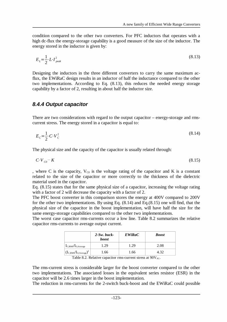
A new family of Efficient Wide Range Converters
condition compared to the other two converters. For PFC inductors that operates with ahigh dc-flux the energy-storage capability is a good measure of the size of the inductor. Theenergy stored in the inductor is given by:
EL=12⋅L⋅I peak
2 (8.13)
Designing the inductors in the three different converters to carry the same maximum ac-flux, the EWiRaC design results in an inductor of half the inductance compared to the othertwo implementations. According to Eq. (8.13), this reduces the needed energy storagecapability by a factor of 2, resulting in about half the inductor size.
8.4.4 Output capacitor
There are two considerations with regard to the output capacitor – energy-storage and rms-current stress. The energy stored in a capacitor is equal to:
EC=12⋅C⋅V C
2 (8.14)
The physical size and the capacity of the capacitor is usually related through:
C⋅V C0=K (8.15)
, where C is the capacity, VC0 is the voltage rating of the capacitor and K is a constantrelated to the size of the capacitor or more correctly to the thickness of the dielectricmaterial used in the capacitor. Eq. (8.15) states that for the same physical size of a capacitor, increasing the voltage ratingwith a factor of 2 will decrease the capacity with a factor of 2. The PFC boost converter in this comparison stores the energy at 400V compared to 200Vfor the other two implementations. By using Eq. (8.14) and Eq.(8.15) one will find, that thephysical size of the capacitor in the boost implementation, will have half the size for thesame energy-storage capabilities compared to the other two implementations.The worst case capacitor rms-currents occur a low line. Table 8.2 summarizes the relativecapacitor rms-currents to average output current.
2-Sw. buck-boost
EWiRaC Boost
IC,RMS/IO,Average 1.29 1.29 2.08
(IC,RMS/IO,Average)2 1.66 1.66 4.32
Table 8.2. Relative capacitor rms-current stress at 90VAC.
The rms-current stress is considerable larger for the boost converter compared to the othertwo implementations. The associated losses in the equivalent series resistor (ESR) in thecapacitor will be 2.6 times larger in the boost implementation. The reduction in rms-currents for the 2-switch buck-boost and the EWiRaC could possible
-123-

High Efficient Rectifiers
be used to reduce the physical size of the capacitor but this has not been investigated. In thiscomparison, the conclusion will be that storing the capacitor energy at a higher voltageusing the standard boost, is preferrable.
8.4.5 EMI-filter
The boost converter has the inductor in series with the input terminals and is therebyobtaining a continuous input current. The filter requirements are relatively small since onlythe inductor ripple current needs to be attenuated by the filter.The EWiRaC converter is of the switchable converter type but the overall topology,independent of the operation mode, is that of a boost converter. As shown in the previoussection, the EWiRaC actually generates less high-frequency ripple current compared to theboost converter for the same inductance.The two-switch buck-boost converter changes topology from the boost to the bucktopology. In the buck mode the input current is highly discontinuous and the generated EMIis significant. In order to give an idea of the filter requirements, consider the followingexample:
The inductor ripple-current in an universal line PFC boost converter is typically designed tobe in the area of +- 10 % of the maximum inductor current [31]. The worst case ripplecurrent occurs at 50% duty-cycle. For the two-switch buck-boost converter operating in thebuck mode with an output voltage of 200V, the worst case EMI is generated at the peak ofthe high line voltage(382V). The duty-cycle is at this point approaching 50%. Thecorresponding high-frequency currents for the boost-mode(EWiRaC) respectively buck-mode operation are shown in Fig. 8.19. The amplitudes are relative to the worst caseconditions and the same power level.
Fig. 8.19. High-frequency ac inductor current. a) Boost current. b) Buck current.
For the purpose of this comparison we will use this worst case condition as an indicator ofthe EMI-filter requirements.
The high-frequency boost current for 50% duty-cycle can be expressed as [32]:
ABoost (n)=(8⋅A1)
(π2⋅n2
)
, n∈[1,3,5,...](8.14)
The high-frequency buck current for 50% duty-cycle can be expressed as [32]:
-124-

A new family of Efficient Wide Range Converters
ABuck (n)=(4⋅A2)
(π⋅n), n∈[1,3,5,...]
(8.15)
The amplitude of the HF ac inductor current, shown in Fig. 8.19a+b for the boostrespectively the buck converter, is related in the following way.
The amplitude A1 for the boost current shown in Fig. 8.19a can be expressed as:
A1=PIN
90⋅ 2⋅0.1
(8.16)
The amplitude A2 for the buck current shown in Fig. 8.19b can be expressed as:
A2=PIN
270⋅ 2
(8.17)
Using Eq. (8.16) and (8.17) the relation between A1 and A2 can be found:
A2=103⋅A1
(8.18)
The EMI-limits regarding conducted noise starts at 150kHz. It is therefore commonpractice, if possible, to choose a switching frequency so this frequency or the next followingharmonics is just below the start of the limits. For this example, a switching frequency of70kHz has been selected. This means that the fundamental and the second harmonic isoutside the area where the regulations apply. The first harmonic to be attenuated is the thirdharmonic of the switching frequency.Using Eq. (8.14), (8.15) and (8.18) the ratio of the third harmonic of the boost and the buckcurrent can be found:
ABuck (3)
ABoost (3)≈15
(8.19)
The EMI-filter in the 2-switch buck-boost should therefore supply 23.5 dB additionalattenuation compared to both the EWiRaC and the boost converter. For a simple second-order L-C filter, this would require, that the cut-off frequency of thefilter is moved 2 octaves down which is equal to a lowering of the cut-off frequency of afactor of 4. The cut-off frequency of the second-order L-C filter is given by:
fωo=
12⋅π⋅ L⋅C
(8.20)
Lowering the cut-off frequency with a factor of 4 would require 16 times the L-C productor 4 times the inductance and 4 times the capacity.
Even though this is a simple comparison, it is clear that the 2 switch buck-boostimplementation requires considerable EMI-filtering compared to the EWiRaC and the boost
-125-

High Efficient Rectifiers
implementations.
8.4.6 Inrush current limiting
For the 2-switch buck-boost converter, there is no additional penalty of controlling theinrush current. As shown in Fig. 8.17a, the 2-switch buck-boost converter has a switch inseries with the input terminals enabling the converter to control the input current. Thelosses in the switch is already accounted for under "Active switches".
The EWiRaC is also able to control the inrush current through the operation of the seriesvoltage-source arrangement. Besides the switches used to implement the voltage-source,there is also the parallel connection of the two primary windings of the transformer. Thesewindings will ad to the conduction losses in the circuit. The amount of losses in thesewindings can almost be arbitrarily small by using a large size transformer or omittedcompletely if the EWiRaC configuration of Fig. 8.10 is used.
For the boost converter additional circuitry is needed to reduce the inrush current. Anelement of some kind, that can control the inrush current has to be placed in series with theoutput capacitor.
8.4.7 Output voltage considerations
Besides the advantage of storing energy at a higher voltage, there is little to suggest, thatthe high bus voltage necessary when using the boost configuration is advantageouscompared to the lower bus voltage supplied by the 2-switch buck-boost and the EWiRaC.The performance of the semiconductor suggest that a lower bus voltage would bepreferable. Also, going towards higher switching frequencies, the parasitic capacitive lossesare reduced by using a lower bus voltage.
8.4.8 Summary
In all of the comparisons carried out in this section, each approach will be ranked accordingto its performance. The best approach receives 1 point, the second best 2 points and theworst approach receives 3 points. In case of a tie, the available points are either split or theranking is split. Table 8.3 summarizes the comparison by accumulating the rankings/pointsgiven to give an overall result of the comparison.
-126-

A new family of Efficient Wide Range Converters
2-Sw. buck-boost
EWiRaC Boost
Active switches 2.5 (2) 1 (1) 2.5 (2)
Diodes 1.5 (1) 1.5 (1) 3 (3)
Inductor 2.5 (2) 1 (1) 2.5 (2)
Outputcapacitor
2.5 (2) 2.5 (2) 1 (1)
EMI-filter 3 (3) 1.5 (1) 1.5 (1)
Inrush current 1 (1) 2 (2) 3 (3)
Output voltage 1.5 (1) 1.5 (1) 3 (3)
Total score 14.5 (12) 11 (9) 15.5 (15)
Table 8.3. Summarized performance of the three approaches at 90VAC.
Based on the categories in this comparison, the EWiRaC has the best performance. Whetherit is reasonable to summarize the performance of the converters as done in table 8.3 isquestionable, since other categories could be added, e.g. cost, that will change the outcome.The cost of implementing new approaches is typically higher, mainly because of two things.The control circuits has to be implemented more or less discrete since commercially ICs arenot available. Power components optimized for the new approach might not be mainstreamcomponents making these more cost sensitive.But the categories of table 8.3 used in this comparison have a direct influence on theefficiency and the performance of the complete power supply system (e.g. the down streamconverter). Another problem with the above approach could be, that each of the categoriesin the comparison, is treated as equally important. If the size of the output capacitor wasdeemed the most significant category the outcome might also change.None the less, it is obvious that the performance of EWiRaC is potentially better than theboost converter and the two-switch buck-boost converter.The comparison is carried out for the worst case situation for both the EWiRaC and theboost converter. As mentioned earlier, the worst case situation for 2-switch buck-boostconverter could also be the high line situation, so the performance of this approach could besomewhat degraded compared to the conclusions of table 8.3.
8.5 Controlling the EWiRaC
The predominant PFC control method for medium to high power PFC boost converters isthe average current mode PFC control. Many commercially control IC's are available forthis control scheme. Another possible control method is the peak current PFC control. Bothwill be presented in this section.Besides the control of the input current and the output voltage, controlling the EWiRaCrequires additional information of the input voltage relative to the output voltage in orderfor the switchable topology scheme to work.
-127-

High Efficient Rectifiers
8.5.1 Overall control considerations
Fig. 8.20. General control scheme of the EWiRaC
Fig. 8.20 shows the general scheme of the control system required to control the EWiRaC.In the standard way, information about the current, input- and output-voltages should beprovided to the PFC controller.From the effective duty-cycle generated by the PFC controller, duty-cycles for the boostswitch and the voltage-source, has to be generated. Information about the mode change hasto be provided to the PWM controller.
Fig. 8.21. Boost (dB(t)) and voltage-source (dVS(t)) duty-cycles as a function of the time varying line voltage.In this example, VOUT is equal to half the line peak voltage.
-128-

A new family of Efficient Wide Range Converters
At high line, the EWiRaC changes operation mode when the input voltage exceeds theoutput voltage. Fig. 8.21 shows how the mode change affects the duty-cycles.The voltage-source duty-cycle, dVS(t), is equal to 1 during the boost mode, and the boostduty-cycle, dB(t), is equal to zero during the voltage-source operation.
8.5.2 Peak current mode PFC control
8.5.2.1 Standard peak current mode control
Peak current mode PFC control is not as common as the average current mode control. Theachievable power factor in a wide-range application, is not as good as with average currentmode control, but it is typically more than 0.98, with low enough harmonic currents tocomply with regulations.In terms of controlling the EWiRaC, the peak current mode PFC control becomes veryattractive since the duty-cycle demanded, seems to jump from effectively zero to effectivelyone. Using standard average current mode control is not an option since this would requirethe output of the error amplifier to change amplitude momentarily when the input voltagereaches the output voltage. Peak current mode control systems are not in the same waylimited by these dynamic restrictions. The standard peak current mode PFC control isshown in Fig. 8.22. Usually, for standard boost converter control, the sensed current isobtained as the switch (Q) current. By sensing the current in this branch, a currenttransformer can be used instead of a sense resister. Since the switch Q, in Fig. 8.22, isinactive during the interval where VIN>VOUT, this method can not be adapted directly. Theinductor current is always flowing in the return path, so placing a sense resistor here enablesthe peak current control.
Fig. 8.22. Peak current mode PFC control scheme.
As for any peak current mode control, instability can occur at duty-cycles above 50%. Sincethe input voltage varies all the way down to zero, duty-cycles above 50% is required tocontrol the current and instability might occur. A well known method of stabilizing the
-129-

High Efficient Rectifiers
converter using peak current mode control, is to ad slope compensation [33].By adding an external slope to the sensed inductor current, the instability can be avoided.The amount of slope required to stabilize the system has to be larger than half the inductorcurrent down slope.
diComp.
dt>
12⋅
diL downslope
dt
(8.21)
The inductor down-slope in a standard boost PFC is varying because of the time varyinginput voltage. In order to stabilize the system, the compensating slope has to be larger thanhalf the largest occurring down-slope, which is when the line voltage reaches zero.A prototype of an EWiRaC using standard peak current mode control is tested in the nextchapter.As the results will show, the standard peak current mode control used for PFC boostconverters, can not be adopted directly.
8.5.2.2 Advanced peak current mode control
For an EWiRaC converter operating at high line, the duty-cycle function will vary from 1 tozero two times compared to the one time for the standard boost converter. This also means,that the maximum down-slope of the inductor current can occur, not only at the zerocrossing of the line voltage, but also at the point, where the input voltage reaches the outputvoltage. If the output voltage is designed to be half the maximum line peak voltage, and thetransformer in the voltage-source uses a 1:1 turns ratio, the inductor down-slope for thetwo worst case occurrences will coincide and the same compensating slope should be ableto be used, both when VIN<VOUT and VIN>VOUT.
Fig. 8.23. Step in input current caused by the standard slope compensation scheme.
-130-

A new family of Efficient Wide Range Converters
As the experimental converter will show, the simple slope compensation scheme is unusablein case of the EWiRaC. In theory, the dynamics of the slope compensation should be able tostabilize the converter, both at the line zero crossing and at the point, where the topology ischanged. But when the input voltage reaches the output voltage, the duty-cycle changesfrom zero to one momentarily which causes a step-change in the reference current.
The current subtracted from the reference current, which make up the slope compensation,is directly proportional to the duty-cycle, so the change in the duty-cycle causes the slopecompensating current to jump from zero to its full value during the mode transition. Thebottom curve in Fig. 8.23 illustrates the change in the compensating current during themode transition. The upper curve in Fig. 8.23, is the resulting line current where thetransition will result in a step change of the current waveform.For a system where the output voltage is placed in the middle of the input range, such thatthe VIN,Peak = 2·VOUT, the required di/dt of the slope is the same for both modes (VIN<VOUT,VIN>VOUT). The step-change in the slope compensating current can be fixed, by shifting adc-current in/out during the transition between the two modes. The magnitude of this dc-current, should be equal to the peak-to-peak compensating current.
Fig. 8.24. Dc-shifted slope compensation.
By shifting the dc-current in/out during the mode transition, the step-change in the slopecompensating current is eliminated and the compensating current undergoes a smoothtransition during the mode change. The dashed line in Fig. 8.24 shows the slopecompensating current without the dc-shifted compensating current as shown in Fig. 8.23.
8.5.3 Average current mode PFC control with level shifted carrier
Average current mode PFC control can be used for the EWiRaC. The switchable converter,BoIBB, shown in chapter 7 Fig. 7.5 has been presented using a modified version of theaverage current mode PFC control [16].The duty-cycle functions of the EWiRaC at high-line, which necessitates a mode change, isshown in Fig. 8.21. As mentioned earlier, the controlling duty-cycle undergoes a stepchange during the transition between the two modes, which makes average mode controlseem like an unusable control strategy because this would require the error amplifier tomomentarily change the control voltage. But if we concentrate on each of the duty-cyclefunctions, dB(t) and dVS(t), we can see that individually, these functions are nice continuousfunctions. So, instead of generating the two different duty-cycle patterns on the backgroundof the master duty-cycle, the duty-cycles should be generated separately but using the same
-131-
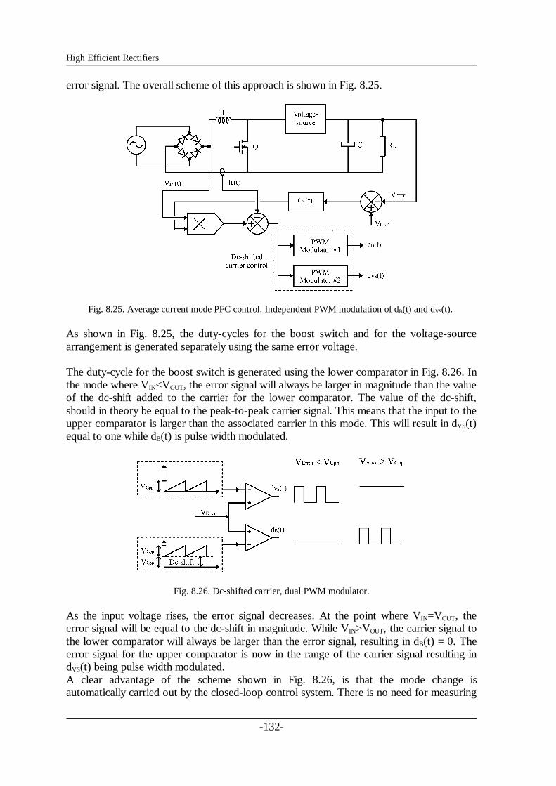
High Efficient Rectifiers
error signal. The overall scheme of this approach is shown in Fig. 8.25.
Fig. 8.25. Average current mode PFC control. Independent PWM modulation of dB(t) and dVS(t).
As shown in Fig. 8.25, the duty-cycles for the boost switch and for the voltage-sourcearrangement is generated separately using the same error voltage.
The duty-cycle for the boost switch is generated using the lower comparator in Fig. 8.26. Inthe mode where VIN<VOUT, the error signal will always be larger in magnitude than the valueof the dc-shift added to the carrier for the lower comparator. The value of the dc-shift,should in theory be equal to the peak-to-peak carrier signal. This means that the input to theupper comparator is larger than the associated carrier in this mode. This will result in dVS(t)equal to one while dB(t) is pulse width modulated.
Fig. 8.26. Dc-shifted carrier, dual PWM modulator.
As the input voltage rises, the error signal decreases. At the point where VIN=VOUT, theerror signal will be equal to the dc-shift in magnitude. While VIN>VOUT, the carrier signal tothe lower comparator will always be larger than the error signal, resulting in dB(t) = 0. Theerror signal for the upper comparator is now in the range of the carrier signal resulting indVS(t) being pulse width modulated. A clear advantage of the scheme shown in Fig. 8.26, is that the mode change isautomatically carried out by the closed-loop control system. There is no need for measuring
-132-

A new family of Efficient Wide Range Converters
the input and output voltage for the purpose of determining the actual mode. For the peakcurrent PFC control scheme, this has to be carried out.
8.5.4 Generating the voltage-source PWM-pattern
After successfully generating the effective duty-cycle function for the voltage-source, thePWM pattern for the individually realizations has to be generated.This PWM pattern is basically the same as the one used for isolated boost converters.
Fig. 8.27. Implementing the voltage-source PWM pattern. a) Logic. b) Generated PWM pattern
The voltage-source pattern generated in Fig. 8.27, is dedicated to the implementations ofthe EWiRaC using two switches in the voltage-source arrangement but is basically the samefor all of the EWiRaC implementations.
8.6 Alternative EWiRaC converters
The EWiRaC solutions presented so far can be characterized as a boost-boost basedswitchable topology which is the fundamental difference compared to other switchabletopologies. The boost-boost topology offers continuous input current using a minimumstress converter (boost). The buck-boost based switchable topologies also uses minimumstress converters but with discontinuous input current in the buck mode. The continuousinput current can be maintained if a boost-buck/boost based topology is used but withincreased converter stress. During the work of constructing the boost-boost based EWiRaCconverters another type of switchable topology emerged which has the continuous inputcurrent but not entirely the characteristics of a boost-buck/boost based topology. This newtype of switchable topology is based on the voltage-source considerations presented in thischapter, but the practical implementation of the voltage-source arrangement differs from theEWiRaCs presented until now. This type of EWiRaC will be referred to as the transformer-less EWiRaC (Patent pending!).
-133-

High Efficient Rectifiers
8.6.1 The transformer-less EWiRaC
Fig. 8.28. Transformer-less EWiRaC
Instead of a transformer based voltage-source, the implementation shown in Fig. 8.28, usesa buck-boost type of converter in series with the output. This actually results in number ofdifferent operation modes of this configuration. The circuit can be related to the conversion lines of Fig. 8.1, using the alternative "1b" and"3" conversions mentioned in section 8.1.1.
8.6.2 The adopted voltage-source operation mode
This mode, follows the operation mode of the EWiRaC converters presented so far. Thesame control strategies can be adopted, except for the fact that the duty-cycle functions tothe voltage-source is reduced to one instead of at least two for the transformer basedEWiRaCs. The operation of the circuit in Fig 8.28 will briefly be explained in the following.
As for the transformer based EWiRaC, the switch Q2 is always turned on (except for currentlimiting situations), when the time varying input voltage is below the output voltage. Theequivalent circuit is similar to the standard boost converter, and the steady-state transferfunction is therefor given by:
V OUT
V IN
=1
1d1
(8.22)
d2=1 (8.23)
For VIN > VOUT the switch Q1 is always turned off and the steady-state transfer function isgiven by:
V OUT
V IN
=d2
d22+1d2
(8.24)
d1=0 (8.25)
-134-
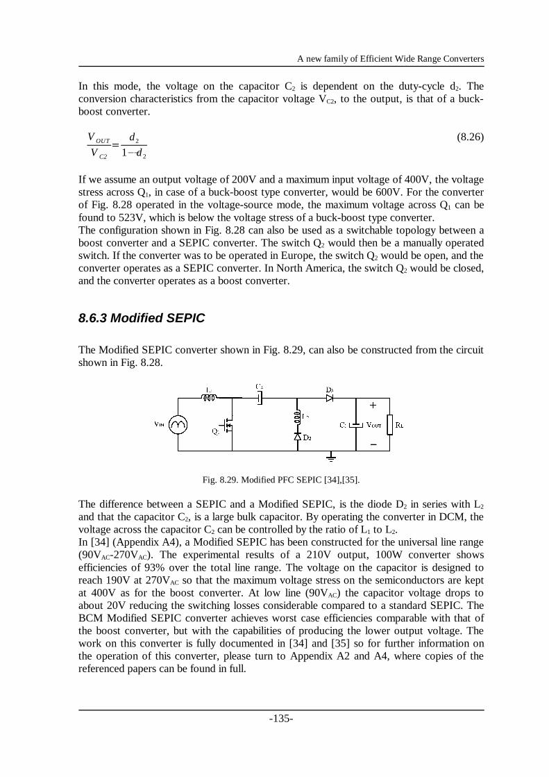
A new family of Efficient Wide Range Converters
In this mode, the voltage on the capacitor C2 is dependent on the duty-cycle d2. Theconversion characteristics from the capacitor voltage VC2, to the output, is that of a buck-boost converter.
V OUT
V C2
=
d2
1d 2
(8.26)
If we assume an output voltage of 200V and a maximum input voltage of 400V, the voltagestress across Q1, in case of a buck-boost type converter, would be 600V. For the converterof Fig. 8.28 operated in the voltage-source mode, the maximum voltage across Q1 can befound to 523V, which is below the voltage stress of a buck-boost type converter.The configuration shown in Fig. 8.28 can also be used as a switchable topology between aboost converter and a SEPIC converter. The switch Q2 would then be a manually operatedswitch. If the converter was to be operated in Europe, the switch Q2 would be open, and theconverter operates as a SEPIC converter. In North America, the switch Q2 would be closed,and the converter operates as a boost converter.
8.6.3 Modified SEPIC
The Modified SEPIC converter shown in Fig. 8.29, can also be constructed from the circuitshown in Fig. 8.28.
Fig. 8.29. Modified PFC SEPIC [34],[35].
The difference between a SEPIC and a Modified SEPIC, is the diode D2 in series with L2
and that the capacitor C2, is a large bulk capacitor. By operating the converter in DCM, thevoltage across the capacitor C2 can be controlled by the ratio of L1 to L2.In [34] (Appendix A4), a Modified SEPIC has been constructed for the universal line range(90VAC-270VAC). The experimental results of a 210V output, 100W converter showsefficiencies of 93% over the total line range. The voltage on the capacitor is designed toreach 190V at 270VAC so that the maximum voltage stress on the semiconductors are keptat 400V as for the boost converter. At low line (90VAC) the capacitor voltage drops toabout 20V reducing the switching losses considerable compared to a standard SEPIC. TheBCM Modified SEPIC converter achieves worst case efficiencies comparable with that ofthe boost converter, but with the capabilities of producing the lower output voltage. Thework on this converter is fully documented in [34] and [35] so for further information onthe operation of this converter, please turn to Appendix A2 and A4, where copies of thereferenced papers can be found in full.
-135-

High Efficient Rectifiers
8.7 Summary
The implementation of the voltage-source approach, solves the most significant problems inthe existing switchable topologies. Since the voltage-source approach facilitates aswitchable topology that uses the boost topology in both modes, the characteristics of theboost converter is maintained throughout the entire input voltage range. This means, thatthe input current does not become discontinuous as it does for other switchable topologies.These new converters based on the voltage-source approach, are called Efficient WideRange Converters (EWiRaC).Designing the converters in order to optimize the worst case condition is also simplifiedsince, as for the boost converter, the worst case situation for the EWiRaC is the largestinput current situation. For other switchable topologies there are typically two situationsthat qualify for the worst case situation, which occurs at both extremes of the input voltagerange.
Several versions of the EWiRaC has been presented together with different controlstrategies. At the present time, the average current mode control with level shifted carrierseems to be the preferred approach. Using this scheme, eliminates the need for a separatemeasurement of the input and output voltage to determine the mode change. Peak current mode control can also be used, especially in the interleaved versions of theEWiRaC, where the peak current mode would be advantageous. A modified slopecompensation scheme has been presented, to solve the problem with the change of referencecurrent during the transition interval.
Furthermore, a comparison between a two-switch buck-boost converter (switchable type), astandard boost converter and the EWiRaC, has been carried out. In this comparison, theEWiRaC demonstrates the lowest overall component stress and thereby shows the potentialof being a high efficiency converter.
For low power applications, the transformer-less EWiRaC is a good alternative to the boostconverter, achieving efficiencies comparable with the boost converter, but with the ability toproduce a medium high output voltage, e.g. 200V.
-136-

Chapter 9
Experimental results
New converter topologies often seems attractive on paper but with disappointingperformance when tested experimental. Prototyping new circuits is the best way to revealany non-ideal behavior of a circuit. In terms of optimizing the power circuit, the EWiRaC isstill in its early phase. The effort put into the experimental work has also been dedicated toverify the operation of the EWiRaC and not so much as to optimize the individually powercomponents. This chapter is devoted to verify the operation of the EWiRaC and show the potential ofthis converter as a very high efficient, wide input range, ac/dc converter. Besides the workthat has been done deriving the power circuit of the EWiRaC, many challenges still exist indesigning the surrounding circuitry e.g. the control system. The functions needed to operatethe EWiRaC can not be implemented with a single control IC, which is possible for the wellknown approaches.The EWiRaC has been tested with two different control strategies and the results of theexperimental work will be presented in the following.
9.1 Prototype specifications
The specifications of the prototypes tested, are given below. The specifications are targetedto be in a typical wide range application in the medium to high power range.
VAC : 90VAC – 260VAC
VOUT : 185VDC
POUT : 500WfSwitching : 70kHz
The switching frequency is selected so that the first and the second harmonic is outside thefrequency band of regulations. The EN55022, which sets the EMI-limits in Europe, starts at150kHz. Similar regulations in the US, also starts at 150kHz.
-137-

High Efficient Rectifiers
9.2 Estimated worst case efficiency of the EWiRaC converter
The worst case operation for the EWiRaC in terms of power losses occurs, as for thestandard boost converter, at low line. The selected power components has not undergone afull optimization process, but based on know-how, reasonable power components havebeen selected to insure high efficiency.In table 9.1, the power components and the associated losses are listed.
Component Type Losses % ofPIN
EMI-filter 2*2.7mH, 8A, Rdc= 22mOhm 1.53W 0.29%
Bridge rectifier GBU8J (8A, 600V) 9.34W 1.76%
Inductor A083081-2, Ve=11cm3, N=60,dCu=0.95mm
3.08
0.58%
MOSFET's Q1 STW45NM50, 80mOhm 5 0.94%
Q2+Q3 SPP20N60S5, 190mOhm 3.7 0.70%
Transformer RM12, Np=43, dCu=0.75mm 1.01 0.19%
Diode STTH806TTI (1 diode) 5.03 0.95%
Total 28.69W 5.41%
Table 9.1 Calculated power losses of the experimental EWiRaC. PIN = 530W, VAC = 90V.
A MathCad spreadsheet of the calculated power losses can be found in Appendix B.
The theoretical losses are calculated using an input power of 530W at VAC = 90V. Theworst case efficiency of the EWiRaC, according to theoretical design, should be in the areaof 94%-95% (94.6%). Using the same components, but in a boost configuration, the losses in Q1 would double,the losses will increase in the inductor and the diode (using both diodes in the tandemconfiguration). The improvements, not counting the losses in the voltage-source, wouldamount to about 2% at low line. The losses in the voltage-source (Q2,Q3 and thetransformer), amounts to almost 1% in efficiency, and the total savings in terms ofefficiency, depends on how efficient, the inrush control of the boost converter can beimplemented.
The EMI filter is constructed as a double-π filter using two common mode chokes. Thedifferential mode chokes are comprised by the leakage inductance of the common modechokes. This can be practical if the large common mode filter is needed, otherwise thisapproach take up a relative large amount of board space.
9.3 Prototype 1: Peak current mode control
The peak current mode control seems like a good choice of control strategy for theEWiRaC. As shown in chapter 8, the effective duty-cycle exhibits a step change from zeroto one and vice versa, in the transition between the two modes of operation.The average current mode PFC control in its original version used in PFC boost converters,
-138-

Experimental results
are not capable of maintaining the control of the input current during the transition.The peak current mode PFC control is not limited in terms of fast duty-cycle changes anddoes therefore seem like a usable control strategy.
The prototype is based on the auto-transformer EWiRaC shown in Fig. 8.11 in chapter 8.Fig. 9.1 is a block schematic of the peak current controlled EWiRaC.
Fig. 9.1. Block schematic of a peak current controlled EWiRaC.
To generate the effective duty-cycle for the EWiRaC, the ML4812 from Fairchild, which isa peak current mode PFC controller, is used. The "Mode selection"-block is a simplecomparator determining whether the input voltage is above or below the output voltage andthereby the mode of operation. The "Logic"-block receives information about the effectiveduty-cycle and the operation mode. Based on these information, the respective duty-cyclefunctions are generated. The duty-cycles are interfaced to the power circuit through thegate drivers IR2110 from International Rectifier [36]. Fig. 9.2 shows the input current of the experimental converter at an input voltage of 90VAC.
-139-

High Efficient Rectifiers
Fig. 9.2. Input voltage and current of the experimental converter of Fig. 9.1. VAC = 90V.
At 90VAC the EWiRaC is only operating in the boost mode. The voltage source is in thismode to be reckoned as a short circuit. Only in case of an over current situations, the powerpath through the voltage-source will be disrupted.For an input voltage of 230VAC, the EWiRaC changes mode. The resulting input current isshown in Fig. 9.3.
Fig. 9.3. Input voltage and current of the experimental converter of Fig. 9.1. VAC = 230V.
This first prototype was not implemented with the advanced slope compensation scheme,which is clearly visible in the current waveform. During the transition between the twomodes of the EWiRaC, the current is more or less out of control. The step change inreference current causes large oscillations as shown in Fig. 9.3. The current waveform, afterthe oscillations have died out, follows a different reference compared to the part of thewaveform before the oscillations as shown in chapter 8, Fig. 8.23.
-140-

Experimental results
Other factors, besides the slope compensation, causes problems near and during thetransition between the two different modes. Peak current control becomes very noisesensitive as the duty-cycle goes to zero. Very narrow pulses can be hard to detect, and atvery small duty-cycles, the peak current controller will go into a pulse-skipping mode.Furthermore, detecting the right time for the change of modes can also introduce distortionduring the transition.A way to overcome the transition problems, is to force the EWiRaC into a third mode ofoperation, which has not been discussed yet. In the third mode of operation, the EWiRaCoperates like a standard boost converter, boosting the voltage up to above the maximumline peak voltage. As the boost switch, Q1, turns off, only one of either Q2 or Q3 is turned onforcing the voltage on the drain connection of the MOSFETs up to twice the outputvoltage, just like a normal boost converter. This will ensure that the duty-cycle will be about50% during the transition. The time at which this mode is entered is not crucial as long as itis before the input voltage reaches the output voltage.The drawback of this approach, is that the inductor current ripple will be twice as largeduring the transition compared to the worst case condition before. The effects in terms ofEMI has not been investigated.
Despite the problems during the transition between the two modes, the performance interms of efficiency of the converter is still very good. The worst case efficiency of theEWiRaC configuration shown in Fig. 9.1, is 94% (Fig.9.4). This configuration uses theflyback snubber shown in Fig. 8.16a, which increased the voltage rating of the switch Q1.Instead, a 600V FET was used (CoolMos : SPW47N60C3 [18]), with higher losses as aresult.
Fig. 9.4. Efficiency of the peak current controlled EWiRaC. VIN = 90VAC
The distortion of the line current has little impact on the efficiencies. At nominal line voltageof 115VAC, the efficiency at full load is 95.6% and at 230VAC the efficiency is 96,5%. Thepeak current control scheme for the EWiRaC is still in its early phase, but development willcontinue in this area. Even though there are good alternatives, as will be shown in the nextsection, the peak current controlled PFC approach has some clear advantages when itcomes to the interleaved EWiRaC approaches.
-141-

High Efficient Rectifiers
9.4 Prototype 2: Average current mode control with level shiftedcarrier
9.4.1 Design considerations
Fig. 9.5. Block schematic of the average current controlled EWiRaC using level shifted carrier.
The peak current controlled EWiRaC, has some disadvantages regarding the transitionbetween the two modes. The instant where VIN=VOUT has to be detected, and the peakcurrent approach has trouble producing very small duty-ratios. These problems can beovercome by using average current mode control with level shifted carrier.To generate the error signal, a standard average current mode PFC controller is used, in thiscase the UCC3817 from Texas Instruments [37].
Fig. 9.6. a) Level shifted carrier approach. b) level shifted error voltage approach.
The two independent duty-cycles is generated by a dual PWM IC (TL1451) [37]. In theTL1451, the carrier is fixed for the two PWM circuits, so for practical reasons, the errorsignal is level shifted instead. Besides containing the carrier signal and the PWM
-142-

Experimental results
comperator, the TL1451 also has two independent error amplifiers. These can be used forconditioning the error signal from the UCC3817.The carrier available in the TL1451 has a peak-to-peak voltage of 0.6V and is level shifted1.4V. The error signal used to generate the duty-cycle for the voltage-source (dVS(t)),should be level shifted as much as the peak-to-peak carrier voltage (VBias = 0.6V). Toprevent a dead zone during the transition, where both of the duty-cycles are inactivebecause of mismatch in the level shifted error signal, the VBias voltage should be reducedbelow the 0.6V. This will create an overlap where both duty-cycles will be active. Theoverlapping of duty-cycles will not result in excessive inductor ripple which is the case forthe peak current controlled EWiRaC in the mode 3 operation discussed in the previoussection.
Fig. 9.7. Simulated average current mode control with level shifted carrier and overlapping duty-cycles.
A dc/dc version of the EWiRaC configuration shown in Fig. 9.5, has been simulated toshow the behavior of the inductor current during the transition. The schematic of the systemcan be found in Appendix C1. The simulation results are shown in Fig. 9.7 and Fig. 9.8.
Fig. 9.8. The inductor current during the transition where VIN exceeds VOUT. This view is a zoom of themarked area in Fig. 9.7.
-143-

High Efficient Rectifiers
For more details on the circuit, see Appendix C1. The input voltage is increased aboveoutput voltage as shown in Fig. 9.7. The current waveform, is set to follow the inputvoltage as it would do in an ac/dc application. Using overlapping duty-cycles, secures asmooth transition. The "Zoom area" shown in Fig. 9.7, can be seen in Fig. 9.8, where a fewsamples of the inductor current is depicted during the transition where the input voltageexceeds the output voltage.The transition shown in Fig. 9.8, is comprised by 3 modes. Mode 1, is the charge mode,where the switch Q1 turns on. The di/dt of the inductor is very high since the maximumapplied inductor voltage occurs in the mode. Mode 2 can be either a charge mode or adischarge mode. In this mode Q1 is turned off, and Q2 and Q3 is turned on. If the inputvoltage is below the output voltage, the inductor di/dt will be negative and the mode is adischarge mode. If the inductor di/dt is positive, the mode is a charge mode. The exact timeof transition can be determined from the inductor di/dt in this mode, as shown in Fig. 9.8.The last mode, mode 3, is a discharge mode where either Q2 or Q3 is turned of.
9.4.2 Performance of the practical implementation
The full schematic of the EWiRaC configuration shown in Fig. 9.5 can be found inAppendix C2. The important power components are listed in table 9.1.
The experimental EWiRaC was first tested as a dc-dc converter. Fig. 9.9 shows the drain-source voltage of the switch Q1 (the boost switch).
The input voltage is 260VDC, which is higher than the output voltage, so in this mode theswitch Q1 is turned off all the time, and Q2 and Q3 is PMW modulated. The voltage on thedrain of Q1 (and Q2,Q3) alternates between the output voltage and twice the output voltage,as expected.
Fig. 9.9. Drain-source voltage of the switch, Q1. The bottom plateau of the waveform is equal to the outputvoltage of 185VDC. The upper plateau is equal to twice the VOUT.
The error signal to the dual PWM driver is shown in Fig. 9.10 and Fig. 9.11 for an ac inputvoltage of 90VAC and 230VAC.
-144-

Experimental results
Fig. 9.10. Line voltage (upper trace) VAC = 90V. Error signal (bottom trace) generated by the UCC3817.
Fig. 9.11. Line voltage (upper trace) VAC = 230V. Error signal (bottom trace) generated by the UCC3817.
In the practical implementation, the output from the dual PWM driver, had to be inverted tomaintain the negative feedback loop. Therefore, the error signal is not varying between1.4V and 2V as we would have expected for the error signal determining the duty-cycle(dB(t)) of the switch Q1. To maintain the proper operation of the circuit, the error signal togenerate dB(t), has to be dc biased. The dc bias was designed to give an overlap ofapproximately 10% to ensure a smooth inductor current transition.Because of the inversion after the dual PWM driver, the error signal to generate thevoltage-source duty-cycle is within the carrier peak-to-peak voltage. We would expect theerror signal to vary with about twice the carrier peak-to-peak voltage, but the inductorcurrent goes into DCM at about 130V at full load and VAC=230V. This minimizes the errorvoltage excursion downwards. Fig. 9.12. shows the input current and voltage at nominal low line voltage (115VAC) and fulloutput power.
-145-

High Efficient Rectifiers
Fig. 9.12. Input voltage and current of the experimental converter of Fig. 9.5. VAC = 115V.
Besides the fact the the input current is almost sinusoidal and in phase with the line voltage(PF=0.999), there are two noticeable distortion phenomenon of the line current. At the zerocrossing of the line voltage we see cusp distortion of the current followed by an overshoot.The cusp distortion is typically because of the di/dt limitations imposed by the inductor, butin this case the inductor is not the limiting factor. The inductor current should be able tofollow the reference current, when the input voltage reaches 0.6V (not including bridgerectifier voltage drop). This should therefore not give rise to the amount of distortionencountered. Because the control system is made of several control ICs, compromises in theinterfacing between these, have resulted in that some of the features, like soft-start, havebeen lost. This can of course be implemented but for the prototype, the problems at start-uphas been fixed by limiting the maximum duty-cycle of the switch Q1. This is the main reasonfor the cusp distortion.The other distortion phenomenon encountered, is the dither at the two extremes of thewaveform. The mode with the overlapping duty-cycles is reached near the top of the115VAC line voltage. This should in theory and as seen with the simulation, not give rise toany problems. One explanation is that the transition generates noise that interfere with thecontrol system. As will be shown later, the PCB design created was not very noise immun.
The harmonic content of the current shown in Fig. 9.12, is very moderate, and compliancewith the regulations is not a problem. For the sake of completeness, the harmonic analysisof the current of Fig. 9.12, is shown in Fig. 9.13.
-146-

Experimental results
Fig. 9.13. Current harmonics in the input current of the experimental converter in Fig. 9.5. VAC = 115V.
At the extreme of the low line range, 135VAC (Fig. 9.14), the converter operates in theoverlapping mode a larger portion of time. Besides the dither distortion, the line currentdistortion caused by the change of mode is moderate.
Fig. 9.14. Input current of the experimental converter in Fig. 9.5. VAC = 135V.
The line current for VAC = 185V is shown in Fig. 9.15. The dither distortion at this inputvoltage is gone, and the transition between the two modes can be seen as a little glitch in thecurrent. The line current is shifted a little to the left, so the transition does not occur at thesame current level.
-147-

High Efficient Rectifiers
Fig. 9.15. Input current of the experimental converter in Fig. 9.5. VAC = 185V.
The drain voltage of Q1,Q2 and Q3 referenced to ground, is shown in Fig. 9.16. The figureillustrates the different modes that the EWiRaC, shown in Fig. 9.5, goes through at highline.
Fig. 9.16. Drain voltage of Q1, Q2 and Q3 referenced to ground. VAC = 185V, VOUT = 185V and POUT = 500W.
In the first mode, the switches Q2 and Q3 are turned on and the switch Q1 is PWMmodulated. This interval is located around the zero crossing of the line and up until theoverlapping duty-cycle mode starts. In the overlapping duty-cycle mode, the drain voltageon the switches varies from zero to VOUT to twice VOUT. In the last mode, the switch Q1 isturned off all the time and the drain voltage is switched between VOUT and twice VOUT.
At the nominal high-line voltage, 230VAC, the noise problems reoccur. The current glitch atthe transition between the modes, can easily be recognized, and besides the cusp distortion,distortion around the line peak voltage occur. It is most likely a noise generatedphenomenon. The duty-cycle signal for the switch Q1 is triggered, and turns on Q1. Thisresults in a high gain of the inductor current which causes instability in the current loop. A
-148-

Experimental results
proper layout and an adjustment of the current loop should take care of these problems.
Fig. 9.17. Input voltage and current of the experimental converter of Fig. 9.5. VAC = 230V.
The harmonic content of the line current is still very low as can be seen from the harmonicanalysis shown in Fig. 9.18.
Fig. 9.18. Current harmonics in the input current of the experimental converter in Fig. 9.5. VAC = 230V.
The efficiency of the EWiRaC at low line is shown in Fig. 9.19 as a function of the outputpower.
-149-

High Efficient Rectifiers
Fig. 9.19. Measured efficiency of the EWiRaC in the low-line range.
The efficiency at 90VAC and full power is 94.8% which is very close to the predicted by thetheoretical calculations of table 9.1. In order to see the effect of the voltage-source on thelosses, a wire was placed across the voltage-source to short circuit it. The losses werereduced with 4W at full power which is slightly below the calculated value. The theoreticalcalculated efficiency is very close to the measured efficiency but this does not mean thatcalculated values are absolutely correct. Different temperatures of the component willinfluence the losses. The purpose of the efficiency calculations was to determine whether the design wascompetitive with the standard boost converter.Besides the relative high efficiency achieved at 90VAC, it is remarkable, that the efficiency ofthe 135VAC is not better than the efficiency at 115VAC. The reason for this is the increasedlosses that the overlapping duty-cycle mode imposes on the converter. This overlappingperiod is going on for about 2/5 of the time (see Fig. 9.12). The efficiency at 115VAC of96.15% is actual higher than the efficiency at 135VAC (96%). This is atypical compared to astandard boost converter, but has no significance, as long as the worst case efficiency is notsacrificed.
Fig. 9.20. Measured efficiency of the EWiRaC in the high-line range.
The efficiency for the high-line range, is shown in Fig. 9.20. In this range, there is a relativesmall difference in the efficiencies at full power (96.5% - 97%). During the interval wherethe input voltage is above the output voltage, power is transferred to the output both in theon and the off periods of the voltage-source duty-cycle. At 185VAC, a larger portion of thepower is supplied to the output during the on period, where the voltage-source is a shortcircuit. As the input voltage increases, the input current decreases, minimizing the effects of
-150-

Experimental results
the voltage-source resistance.
Fig. 9.21. Measured efficiency of the EWiRaC at full output power, 500W, as a function of the line voltage.
The efficiency as a function of the line voltage at full output power, is shown in Fig. 9.21.As explained earlier, the efficiency at 135VAC is slightly lower because of the overlappingduty-cycle mode. Other wise, the intended improved efficiency at low-line has beenachieved with approximately 1-2 percentage points, dependent on the implementation of theinrush current limiter. The high line efficiency does not seem to suffer from the EWiRaCoperation mode.
In all of the efficiency measurements, the auxiliary supply has not been accounted for, andwas measured to about 2W. Further more, as can be seen in Fig. 9.21, the input voltagerange was reduced to 255VAC, because of the noise induced instability at the high inputline. This, on the other hand, does not have any consequences for the achievedperformance.
9.5 Summary
The efficiency improvements obtained using the EWiRaC compared to a standard boostconverter, has been estimated to be in the range of 1-2% percentage points, mostlydependent on how efficient the inrush current limiter is implemented. This means, that astate-of-the-art implementation of a hard-switched CCM boost PFC for the universal linerange, should achieve efficiencies in the range of 92.5%-93.5% whereas the EWiRaCshould achieve an efficiency of about 94.5% which reduces the power losses with about15% to 30%.
In order to verify the high efficiency capability of the EWiRaC, the results obtained on twoprototypes have been reported.The first prototype was implemented using standard peak current mode control. Aspredicted, in chapter 8, the transition between the two modes causes problems. The effectof not using the improved slope compensation scheme is clearly visible in the line currentwaveform. Besides the problems with the slope compensation, other factors were pointedout, such as the problems that can occur when narrow duty-cycles are demanded by thepeak current mode controller. A way to solve these problems, would be to go into thestandard boost mode in a narrow interval around the mode change. Thereby, the converter
-151-

High Efficient Rectifiers
would operate with an effective duty-cycle close to 50% assuming that the output voltage isselected in the middle of the line range.Despite the above mentioned problems, the efficiency of the converter was relatively good(94%). For the main switch (Q1), a different type MOSFET with a voltage rating of 600Vwas used, which was not as good as the one listed in table 9.1. The second prototype was implemented using the average current mode control with levelshifted carrier. Besides the experimental converter, simulated results, showing the behaviorof the inductor current during the mode change, has also been presented. The worst caseefficiency reached 94.8%, thereby verifying the predicted quality of the EWiRaC as a highefficient wide input range converter.
-152-

Chapter 10
Conclusion
The overall goal of this thesis has been to provide the knowledge and the understanding thatcan lead to an increased efficiency for ac/dc power systems complying with EN61000-3-2 inwide input range applications. The first part of the thesis focus on the different approaches that can be taken to provide thenecessary ac/dc conversion for compliance with the regulations. For a majority of theresearch in ac/dc conversion, the focus has been on integrating the PFC-unit into theexisting dc/dc converter and one of the tasks in this thesis has been to analyze the effects onthe conversion efficiency by doing this. The two major groups of alternative PFC solutionshave been recognized as the Reduced Power Processing approach and the Single-Stageapproach. In order to investigate the performance of the different approaches, the basic convertertopologies, both isolated and non-isolated, have been analyzed in terms of componentstress, in chapter 5. Several important observations were made in this process. The twomost important observations with direct influence on how the different PFC approachesperform are listed below.
Non-isolated buck and boost type converters are low component stress converterscompared to the buck-boost type converters.
Isolated buck and boost converters have increased semiconductor component stress, andexhibits a dramatically increase in these stresses when exposed to input voltagevariations.
In the Reduced Power Processing approach a typically way of evaluating the performanceof this approach, is to calculate the amount of power processing. In this evaluation the Two-Stage approach is used as the worst case approach with its two-times of power processing,calculated as one time for the PFC pre-converter, and one time for the isolated dc/dcconverter.As shown in chapter 6, the amount of power processed is a very poor indicator of howefficient the conversion is performed and in all practical cases, the Reduced PowerProcessing approaches expose the components to a higher stress compared to the Two-
-153-

High Efficient Rectifiers
Stage approach. The reason for this, is that the Reduced Power Processing approach has tomake use of high component stress converters (buck-boost derived) and/or isolatedconverters in high stress configurations. The basic conclusion is: It is not how much, but inwhat way the power is processed, that is the determining factor on the components stressesand thereby the efficiency.
The Single-Stage approach is comprised of an isolated dc/dc converter with means to shapethe input current so that compliance with the regulations is possible. The output voltage isregulated with a fast control loop, and the Single-Stage approach does not rely on aseparate control system to regulate the input current. In order to decouple the pulsatinginput power, a large bulk capacitor serves as the energy storage. Since there is only onecontrol system regulating the output voltage, the storage capacitor voltage is not directlyregulated. This voltage depends on the input/output power balance, and will typically varyproportional to the line voltage. This means, that for a 3:1 ac input-voltage range, the inputto the isolated dc/dc converter will also be exposed to a 3:1 voltage range. Therefore, asshown in chapter 6, the Achilles heal of the Single-Stage approach, is the isolated dc/dcconverter-part.The varying input voltage will expose the power semiconductors to excessive stressresulting in the Two-Stage approach to be more efficient. For the best Single-Stageconfigurations, the approach becomes competitive with the Two-Stage approach when theinput voltage range is reduced to about 1.3:1. This means that for very narrow voltagerange applications, the best of the Single-Stage approaches might be a reasonable solution.
For wide input applications, the Two-Stage approach, using a boost PFC, is the superiorapproach compared to the Reduced Power Processing approach and the Single-Stageapproach.
Even though the boost converter is a low component stress converter, the voltage variationis still the limiting factor on the efficiency. Since the boost converter is only able to producean output voltage larger than the maximum line peak voltage, the worst case situation forthe converter is at low line, where the step-up ratio is maximized. Other PFC pre-convertersexists that are capable of producing an output voltage below the maximum line peakvoltage. The SEPIC converter is capable of this, but because the converter is a buck-boostderived converter, the component stresses are high with reduced efficiency as aconsequence. Besides the lower output voltage, the SEPIC is also capable of controlling theinrush current, which is something that the boost converter is unable to do, unless extracircuitry is provided. Switchable topologies like the two-switch buck-boost is a better approach compared to theSEPIC. This converter is able to change the topology from being a boost type to a bucktype according to the instantaneous value of the line voltage. If the line voltage is below theoutput voltage the converter works in the boost mode and in the buck mode if the linevoltage is above the output voltage. The most significant drawbacks of this approach is, thatall the input power has to flow through the buck switch, and that in the buck mode, theinput current becomes highly discontinuous, increasing the EMI filtering requirements.
All of the above investigations, considerations and observations, have lead to theconstruction of a new type of PFC converter that addresses the problems with the boostconverter but retain its efficient conversion properties.
-154-

Conclusion
This new converter has been named Efficient Wide Range Converter (EWiRaC) andpossesses the following features.
High efficiency Output voltage below the line peak voltage Continuous input current (low EMI-filter requirements) Inrush-current limiting
Several versions of the EWiRaC have been presented, all which are based on an approachcalled the series voltage-source approach. This approach makes it possible to effectivelyreduce the input voltage range with a factor of two.The EWiRaC has been compared with both the two-switch buck-boost and the standardboost converter. The results of this comparison showed, that the EWiRaC potentially wouldbe able to achieve higher efficiency compared to both the two-switch buck-boost, and thestandard boost converter.
To verify the performance of the EWiRaC, two prototypes have been presented usingdifferent control schemes. The EWiRaC was designed for the universal line range with anoutput voltage of 185VDC capable of 500W output power. The peak current controlled EWiRaC exhibited problems in the region where the modechange occurs resulting in distortion and large oscillations in the input current. Despite theless successfully implemented control scheme, the efficiency at 90VAC and full powerreached 94%.The second prototype used average current mode control with level shifted carriers. Besidessome noise-related problems at voltages approaching the upper limit of the input voltage,this control scheme exhibits an almost unnoticeable mode change. Furthermore, theefficiency reached with this prototype was 94,8% and for the full line range, the worst caseefficiency was in the range of 94,8%-97%. For a boost PFC converter using the same power components, the efficiency will be at least1-2 percentage points lower, which translates into a reduction of the power losses of 15%-30% by using the EWiRaC.
The complexity of the EWiRaC is relatively large, mainly because of the associated controlcircuitry. Since the EWiRaC is a new invention, commercially control ICs are not availablethat collects all of the control features into a single package. When this becomes a reality,the complexity will reduce considerable.
-155-

High Efficient Rectifiers
Blank page
-156-

References (thesis)
In the thesis, two different reference systems are used. In the first system, the references arenumber consecutively after when they appear in the thesis. The second system covers thereferences in the database. These references uses the database reference number with "db"added in front. The database reference list is called "References (database)" and can befound in the following section.
[1] K. Billings, "Switchmode power supply handbook",second edition, Mcgraw-Hill 1999.
[2] Measurements on standard off-the-shelf power supplies. Truls Andersen,Powerlab (www.powerlab.dk) and Lars Petersen, Technical University of Denmark, 2000.
[3] O. Garcia, J.A. Cobos, R. Prieto, P. Alou and J. Uceda, "Simple ac/dc converters to meet IEC 1000-3-2", APEC 2000, pp. 487-493.
[4] N. Mohan, T.M. Undeland, W.P. Robbins," Power Electronics", 2nd edition, 1995 Wiley & Sons.
[5] R.W. Erickson, D. Maksimovic, "Fundamentals of Power Electronics", 2nd edition, 2001 Kluwer Academic Publishers.
[6] Villegas, P.J.; Sebastian, J.; Hernando, M.; Nuno, F.; Martinez, J.A.; Power Electronics, IEEE Transactions on , Volume: 15 Issue: 5 , Sept. 2000 pp.813 -819.
[7] O. Garcia, J.A. Cobos, R. Prieto, P. Alou and J. Uceda, "A new approach for single stage AC/DC power factor correction converters with an improved energy processing", PESC 1998, pp. 1061-1067.
[8] E. Rodriguez, O. Garcia, J.A. Cobos, J. Arau and J. Uceda, "A single-stage rectifier with PFC and fast regulation of the output voltage", PESC 1998, pp. 1642-1648.
[9] O. Garcia, P. Alou, J.A. Oliver, J.A. Cobos, J. Uceda and S. Ollero, "AC/DC converters with tight output voltage regulation and with a single control loop", APEC 1999, pp. 1098-1104.
[10] Lars Petersen, "Advantages of using a two-switch forward in single-stage power factor corrected power supplies", INTELEC 2000, pp. 325-331.
-157-

High Efficient Rectifiers
[11] A. Fernandez, A. Ferreres, P. Villegas, J. Sebastian and L. Alvarez, "Size comparison between a half bridge converter with an AICS and a two-stage boost converter operating in a narrow input voltage range", PESC 2001, pp. 1793-1798.
[12] L. Petersen and M. Andersen, "Two-stage power factor corrected power supplies: The low component-stress approach", APEC 2002, pp. 1195-1201
[13] Christian Wolf, "Ensrettere med sinusformet netstrøm", Ph.d.-thesis, Institut for Automation, Technical University of Denmark, 1995.
[14] M.A.E. Andersen, "Fast prediction of differential mode noise input filter requirements for flyback and boost unity power factor converters", EPE
1997, pp. 2.806-2.809.
[15] Bruce Carsten, “Converter component load factors; A performance limitation of various topologies”, PCI 1988, Munich
[16] J. Chen, D. Maksimovic, R. Erickson, "A new low-stress buck-boost converter for universal-input PFC applications", APEC 2001, pp. 343-349.
[17] I. Lindroth, P. Melchert, T. Sahlstrom, "Methods of improving efficiency in wide input range boost converters at low input voltage", Intelec proc. 2000, pp. 424-431.
[18] [www.infineon.com]
[19] Correspondence with Dr. Gerald Deboy, head of High voltage MOS development, Infineon Technologies AG, Power management & supplies.
[20] M.A.E. Andersen et al., "Basic power electronics" (in Danish), 1997, Dep. of Automation, Technical University of Denmark.
[21] O. Garcia, J.A. Cobos, P. Alou, R. Prieto, J. Uceda, S. Ollero, “A new family of single stage AC/DC power factor correction converters with fast output voltage variation”, PESC Proc. 1997, pp. 536-542
[22] A. J. Calleja, J. M. Alonso, J. Ribas, E. L. Corominas, M. Rico-Secades, J. Sebastian, "Design and experimental results of an input-current-shaper based electronic ballast", IEEE Transactions on Power Electronics, VOL. 18, NO. 2, March 2003, pp.547-557
[23] J.G. Kassakian et al. "Principles of Power Electronics", Addison-Wesley 1992.
[24] www.vicr.com
[25] www.vicr.com/products/datasheets/ds_vi-ham.pdf
[26] J. Sebastian, A. Fernandez, P.J. Villegas, M.M. Hernando, J.M. Lopera, "Improved active input current shapers for converters with symmetrically
-158-

driven transformer", IEEE Transactions on Industry Applications, VOL. 37, O. 2, March 2001, pp.592-600
[27] J. Chen, "Topologies and control of low harmonic rectifiers", Ph.D. Thesis, Department of Electrical and Computer Engineering, University of Colorado at Boulder. 2002.
[28] De Aragao Filho, W.C.P.; Barbi, I.,"A comparison between two current-fed push-pull DC-DC converters-analysis, design and experimentation", INTELEC 1996, pp. 313-320.
[29] C. Peng, M. Hannigan, O. Seiersen, "A new efficient high frequency rectifier circuit", Proceedings of High Frequency Power Conversion 1991, pp. 236-243.
[30] [www.st.com]
[31] Unitrode power supply design seminar, SEM-1000, topic 1: J. Noon, "A 250kHz,500W power factor correction circuit employing zero voltage switching".
[32] Elektronik Ståbi, 7. udgave, Teknisk Forlag A/S 1995. ISBN 87-571-1481-1
[33] D. M. Mitchell, "DC-DC switching regulator analysis", DMMitchell consultants 1992.
[34] Lars Petersen, Robert W. Erickson, "Reduction of voltage stresses in buck-boost-type power factor correctors operated in boundary conduction mode", APEC 2003, pp. 664-670
[35] Lars Petersen, "Input-current shaper based on a modified SEPIC converter with low voltage stress",PESC 2001, pp. 666-671
[36] www.irf.com
[37] www.ti.com
[38] P.C. Todd, "Snubber cicuits: Theory, design and application", Unitrode design seminar, SEM1000, P4.
-159-

High Efficient Rectifiers
Blank page
-160-

References (database)
[db1] Laszlo Balogh, "Power-Factor Correction with Interleaved Boost Converters in Continuous-Inductor-Current Mode", APEC 1993, pp. 168-174
[db2] P. Tenti, C. Licitra, G. Spiazzi, B. Fabiano, L. Rossetto, "Fast-Response High-Quality Rectifier With Sliding-Mode Control", APEC 1993, pp. 175-181
[db3] Roberto Martinez, Prasad N. Enjeti, "A High Performance Single Phase AC to DC Rectifier with Input Power Factor Correction", APEC 1993, pp. 190-195
[db4] Eric X. Yang, Yimin Jiang, Fred C Lee, Guichao Hua, "Isolated Boost Circuit forPower Factor Correction", APEC 1993, pp. 196-203
[db5] Jih-Sheng Lai, Daoshen Chen, "Design Consideration for Power Factor Correction Boost Converter Operating at the Boundary of Continous ConductionMode and Discontinuous Conduction Mode", APEC 1993, pp. 267-273
[db6] G. K. Dubey, M. S. Dawande, "Programmable Input Power Factor Correction Method For Switch Mode Rectifiers", APEC 1993, pp. 274-280
[db7] James J. Spangler, Anup K. Behera, "A Comparison Between Hysteretic and Fixed Frequency Boost Converters Used For Power Factor Correction", APEC 1993, pp. 281-286
[db8] Yimin Jiang, Wei Tang, Fred C Lee, Guichao Hua, "A Novel Single-Phase Power Factor Correction Scheme", APEC 1993, pp. 287-292
[db9] Wei Tang, Yimin Jiang, Guichao Hua, Fred C Lee, I. Cohen, "Power Factor Correction With Flyback Converter Employing Charge Control", APEC 1993, pp. 293-298
[db10] William F. Yadusky, Arthur W. Kelley, "Rectifier desing for minimum line current harmonics and maximum power factor", APEC 1989, pp. 13-22
[db11] G. Joos, P. D. Ziogas, M. Kazerani, "Programmable input powerfactor correctionmethods for single phase diode rectifier circuits", APEC 1990, pp. 177-184
[db12] Mehmet K. Nalbant, "Power factor calculations and measurements", APEC 1990, pp. 543-552
-161-

High Efficient Rectifiers
[db13] S. A. Oliveira da Silva, Ivo Barbi, "Sinusoidal line current rectification at unity power factor with boost quasi-resonant converters", APEC 1990, pp. 553-562
[db14] C. D. Manning, K. A. Amarasinghe, "A resonance power supply that provides dynamic power factor correction in capacitor input off-line converters", APEC 1990, pp. 563-570
[db15] JHR Enslin, GL Van Harmelen, "Real-time, dynamic controller for dynamic power filters in supplies with high contamination", APEC 1990, pp. 571-578
[db16] Mark A. Geisler, "Predicting power factor and other input parameters for switching power supplies", APEC 1990, pp. 579-587
[db17] William F. Yadusky, Arthur W. Kelley, "Phase-controlled rectifier line-current harmonics and power factor as a function of firing angle and output filter inductance", APEC 1990, pp. 588-597
[db18] Michael Madigan, Robert Erickson, Sigmund Singer, "Design of a simple high-power-factor rectifier based on the flyback converter", APEC 1990, pp. 792-801
[db19] Robert L. Steigerwald, Mustansir H. Kheraluwala, Michael J. Schutten, "Characteristics of load resonant converters operated in a high power factor mode", APEC 1991, pp. 5-16
[db20] Michael D. Moore, Arthur W. Kelley, James L. Nance, Mohab A. Hallouda, "Near unity power factor single phase AC to DC converter using a phase controlled rectifier", APEC 1991, pp. 387-392
[db21] James J. Spangler, Anup K. Behera, Badruzzaman Hussain, "Electronic fluorescent ballast using a power factor correction technique for loads greater than 300 W", APEC 1991, pp. 393-399
[db22] R. Krishnan, Geunhie Rim, "AC to DC power conversion with unity power factor and sinusoidal input current", APEC 1991, pp. 400-406
[db23] M. S. Elmore, W. A. Peterson, S. D. Sherwood, "A power factor enhancement circuit", APEC 1991, pp. 407-414
[db24] Jih-Sheng Lai, Tom Key, Don Hurst, "Switch-mode power supply power factor improvement via harmonic elimination methods", APEC 1991, pp. 415-422
[db25] Richard Hoft, Soonwook Hong, Ray Hudson, "Modeling and simulation of a digitally controlled active rectifier for power conditioning", APEC 1991, pp. 423-429
[db26] Carlos Alberto Canesin, Ivo Barbi, "A unity power factor multiple isolated outputs switching mode power supply using a single switch", APEC 1991, pp. 430-436
[db27] James M. Simonelli, David A. Torrey, "Input filter design considerations for boost-derived high power-factor converters", APEC 1992, pp. 186-192
-162-

[db28] Laszlo Balogh, Richard Redl, "RMS, DC, peak, and harmonic currents in high-frequency power-factor correctors with capacitive energy storage", APEC 1992, pp. 533-540
[db29] Roger J. King, Douglass B. Robless, "A 1-kW unity-power-factor rectifier with isolation and fault protection", APEC 1992, pp. 541-548
[db30] John C. Salmon, "Circuit topologies for single-phase voltage-doubler boost rectifiers.", APEC 1992, pp. 549-556
[db31] David M. Otten, Martin F. Schlecht, Brett A. Miwa, "High efficiency power factor correction using interleaving techniques", APEC 1992, pp. 557-568
[db32] Bonanni Ignazio, "High power factor resonant rectifier for UPS systems", APEC1992, pp. 594-597
[db33] A. R. Prasad, S. Manias, P. D. Ziogas, "A new active power factor correction method for single-phase buck-boost AC-DC converter", APEC 1992, pp. 814-820
[db34] Harold Seidel, "A power factor tuned class D converter", PESC 1988, pp. 1038-1042
[db35] Kwang-Hwa Liu, Yung-Lin Lin, "Current waveform distortion in power factor correction circuits employing discontinuous-mode boost converters", PESC 1989, pp. 825-829
[db36] Sigmund Singer, "The application of the "Loss-Free Resistors" in power processing circuits", PESC 1989, pp. 843-846
[db37] James B. Williams, "Design of feedback loop in unity power factor AC to DC converter", PESC 1989, pp. 959-967
[db38] G. Verghese, J. Thottuvelil, A. Heyman, K. Mahabir, "Linear averaged and sampled data models for large signal control of high power factor AC-DC converters", PESC 1990, pp. 372-381
[db39] Chen Zhou, Raymond B. Ridley, Fred C Lee, "Design and analysis of a hystereticboost power factor correction circuit", PESC 1990, pp. 800-807
[db40] J. A. Cobos, J. Sebastian, J. Uceda, J. Arau, F. Aldana, "Improving power factorcorrection in distributed power supply systems using PWM and ZCS-QR SEPICtopologies", PESC 1991, pp. 780-791
[db41] Robert L. Steigerwald, Mustansir H. Kheraluwala, Ramachandran Gurumoorthy,"A fast response high power factor converter with a single power stage", PESC 1991, pp. 769-779
[db42] Do-Hyun Jang, Jong-Soo Won, Gyu-Ha Choe, "Asymmetrical PWM method forAC chopper with improved input power factor", PESC 1991, pp. 838-845
[db43] Karel Jezernik, Franc Mihalic, Miro Milanovic, Uros Milutinovic, "Single phase
-163-

High Efficient Rectifiers
unity power factor correction circuits with coupled inductance", PECS 1992, pp.1077-1082
[db44] J. A. Cobos, J. Sebastian, J. Uceda, P. Gil, F. Aldana, "Analysis of the zero-current-switched quasiresonant converters used as power factor preregulators", PESC 1992, pp. 1052-1060
[db45] Gyu-Ha Choe, Dong Y. Huh, Hack S. Kim, "New group of ZVS PWM converters operable on constant frequency and its application to power factor correction circuit", PESC 1992, pp. 1441-1446
[db46] I. Batarseh, C. Q. Lee, Rui Liu, "A unified approach to the design of resonant power factor correction circuits", PESC 1992, pp. 181-188
[db47] Bo H Cho, Fakhralden A Huliehel, Fred C Lee, "Small-signal modelling of the single-phase boost high power factor converter with constant frequency control",PESC 1992, pp. 475-482
[db48] Andre S Kislovski, Richard Redl, "Source impedance and current-controlled loopinteraction in high-frequency power-factor correctors", PESC 1992, pp. 483-488
[db49] Toshiyuki Sugiura, Takashi Yamashita, Hisahito Endo, "A high-power-factor buck converter", PESC 1992, pp. 1071-1076
[db50] Rui Liu, C. Q. Lee, I. Batarseh, "Resonant power factor correction circuits with resonant capacitor-voltage and inductor-current-programmed controls", PESC 1993, pp. 675-680
[db51] Domingos S.L. Simonetti, J. Uceda, J. Sebastian, "A small-signal model for sepic, cuk and flyback converters as power factor preregulators in discontinous conduction mode", PESC 1993, pp. 735-741
[db52] Sam Ben-Yaakov, Gregory Ivensky, Alexander Abramovizt, "A resonant power factor conditioner", PESC 1993, pp. 995-1001
[db53] Widodo Sulistyono, Prasad N. Enjeti, "A series resonant AC-to-DC rectifier withhigh-frequency isolation", APEC 1994, pp. 397-403
[db54] L C de Freitas, A V da Costa, C H. G. Treviso, "A new ZCS-ZVS-PWM boost converter with unit power factor operation", APEC 1994, pp. 404-410
[db55] Fred C Lee, Guichao Hua, R Watson, "Characterization of an active clamp flyback topology for power factor correction applications", APEC 1994, pp. 412-418
[db56] Ed Deng, Slobodan Cuk, "Single stage, high power factor, lamp ballast", APEC 1994, pp. 441-449
[db57] Y Nishida, T Haneyoshi, E Ohtsuji, O Miyashita, "High power factor PWM rectifiers with an analog pulse-width predictor", APEC 1994, pp. 563-568
[db58] Esam Ismail, Robert Erickson, Michael Madigan, "Integrated high quality
-164-

rectifier-regulators", PESC 1992, pp. 1043-1051
[db59] J. A. Cobos, J. Uceda, J. Sebastian, P. Gil, "The determination of the boundariesbetween contintinuous and discontinuous conduction modes in PWM DC-to-DC converters used as power factor preregulators", PESC 1992, pp. 1061-1070
[db60] Mila M. Jovanovic, Dan M.C. Tsang, Fred C Lee, "Reduction of voltage stress inintegrated high-quality rectifier-regulators by variable-frequency control", APEC1994, pp. 569-575
[db61] Richard Redl, Jiatian Hong, Iftikhar Khan, Dragan Maksimovic, Robert Erickson, "Half-cycle control of the parallel resonant converter operated as a highpower factor rectifier", APEC 1994, pp. 556-562
[db62] Sarma Mulukutla, C Michael Hoff, "Analysis of the instability of PFC power supplies with various AC sources", 1994 1994, pp. 696-702
[db63] Brian P Erisman, Laszlo Balogh, "Reducing distortion in peak-current-controlledboost power-factor correctors.", APEC 1994, pp. 576-583
[db64] John O'Connor, John Bazinet, "Analysis and design of a zero voltage transition power factor correction circuit", APEC 1994, pp. 591-597
[db65] Dragan Maksimovic, "Design of the clamped-current high-power-factor boost rectifier", APEC 1994, pp. 584-590
[db66] Laszlo Balogh, Richard Redl, "Design considerations for single-stage isolated power-factor-corrected power supplies with fast regulation of the output", APEC1995, pp. 454-458
[db67] John C. Salmon, "Performance of a 1-phase buck-boost rectifier using two coupled windings and a spilt dc-rail output voltage", APEC 1995, pp. 427-433
[db68] Michael T Zhang, Mila M. Jovanovic, Fred C Lee, Yimin Jiang, "Single-phase three-level boost power factor correction converter", APEC 1995, pp. 434-439
[db69] L C de Freitas, Joao L Andres, Adriano Alves Perira, "A high power factor operating self-resonant-PWM forward converter", APEC 1995, pp. 440-446
[db70] Milivoje Brkovic, Slobodan Cuk, "Novel single-stage AC-to-DC converters withmagnetic amplifiers and high power factor", APEC 1995, pp. 447-453
[db71] Dragan Maksimovic, Robert Erickson, "Universal-input, high-power-factor, boost doubler rectifiers", APEC 1995, pp. 459-465
[db72] Richard Redl, Laszlo Balogh, "Power-factor correction in bridge and voltage-doubler rectifier circuits with inductors and capacitors", APEC 1995, pp. 466-472
[db73] DaFeng Weng, S. Yuvarajan, "Constant-switching-frequency AC-DC converter using second-harmonic-injected PWM", APEC 1995, pp. 642-646
-165-

High Efficient Rectifiers
[db74] Yungteak Jang, Dragan Maksimovic, Robert Erickson, "Nonlinear-carrier controlfor high power factor boost rectifiers", APEC 1995, pp. 635-641
[db75] John C. Salmon, "Circuit topologies for pwm boost rectifiers operated from 1-phase and 3-phase ac supplies and using either single or split dc rail voltage outputs", APEC 1995, pp. 473-479
[db76] V. Belaguli, A K.S. Bhat, "Operation of LCC-type parallel resonant converter asa low harmonic rectifier", APEC 1996, pp. 131-137
[db77] D. Balocco, C. Zardini, "The half-wave quasi-resonant ZCS flyback converter asan automatic power factor preregulator : an evaluation", APEC 1996, pp. 138-144
[db78] M. S. Elmore, "Input current ripple cancellation in synchronized, parallel connected critically continuous boost converters", APEC 1996, pp. 152-158
[db79] Dragan Maksimovic, Carlos Oliveira, "Zero-current-transition converters for high-power-factor AC/DC applications", APEC 1996, pp. 159-165
[db80] P. P. Mok, C. S. Moo, "Multi-resonant boost converter as active filter for powerfactor correction", APEC 1996, pp. 166-171
[db81] Praveen Jain, Gerry Moschopoulos, G. Joos, "Practical design considerations fora zero-voltage switched power factor correction converter", APEC 1996, pp. 172-178
[db82] Chin-Yuan Hsu, Horng-Yuan Wu, "A new single-phase active power filter with reduced energy storage capacitor", PESC 1995, pp. 202-208
[db83] L. Rossetto, P. Mattavelli, G. Spiazzi, "Power factor preregulators with improveddynamic response", PESC 1995, pp. 150-156
[db84] Ned Mohan, Franz C. Zach, Girish R Kamath, Johann W Kolar, "Self-adjusting input current ripple cancellation of coupled parallel connected hysteresis-controlled boost power factor correctors", PESC 1995, pp. 164-173
[db85] John S. Glaser, Arthur F. Witulski, "Desing issues for high power factor AC-DCconverter systems", PESC 1995, pp. 542-548
[db86] W. Shireen, G. Arun, Prasad N. Enjeti, "Improved active power factor correctioncircuit using a zero voltage switching boost converter", PESC 1995, pp. 701-706
[db87] A. Kandianis, S. Manias, G. Kostakis, "Novel boost converter topologies with zero switching losses for DC-DC and AC-DC applications", PESC 1995, pp. 707-713
[db88] J. Uceda, J. Sebastian, C. Aguilar, F. Canales, "An integrated charger/dischargerwith power factor correction", PESC 1995, pp. 714-719
[db89] Milivoje Brkovic, Slobodan Cuk, "Anovel single stage AC-to-DC full-bridge converter with magnetic amplifiers for input current shaping", PESC 1995, pp.
-166-

990-995
[db90] J. R. Pinheiro, H. A. Grundling, D. L.R. Vidor, "Dual output three-level boost power factor correction converter with unbalanced loads", PESC 1996, pp. 733-739
[db91] M. H.L. Chow, C. K. Tse, "Single stage high power factor converter using the Sheppard-Taylor topology", PESC 1996, pp. 1191-1197
[db92] Xiao-Ming Yuan, Wei-Xun Lin, Laszlo Balogh, Jin-Fa Zhang, Hong-Ying Wu, "Single-phase unity power factor current-source rectification with buck-type input", PESC 1996, pp. 1149-1154
[db93] Konrad Mauch, Jing Wang, William G. Dunford, "A fixed frequency, fixed dutycycle boost converter with ripple free input inductor current for unity power factor operation.", PESC 1996, pp. 1177-1183
[db94] Ivo Barbi, Grover V. Torrico Bascope, ""Isolated flyback-current-fed push-pull converter for power factor correction"", PESC 1996, pp. 1184-1190
[db95] J. A. Ferreira, M van der Berg, "A family of low EMI, unity power factor correctors", PESC 1996, pp. 1120-1127
[db96] J. Uceda, Domingos S.L. Simonetti, J. A. Cobos, J. Sebastian, "Analysis of the conduction boundary of a boost PFP fed by universal input", PESC 1996, pp. 1204-1208
[db97] Y. Murai, K. Kamiya, M. Matsubara, "Soft-switched single-phase AC/DC converter circuit with sinusoidal input-current", PESC 1996, pp. 159-164
[db98] M. Daniele, Praveen Jain, G. Joos, "A single stage single switch power factor corrected AC/DC converter", PESC 1996, pp. 216-222
[db99] C. Q. Lee, Joel P. Gegner, "Linear peak current mode control: A simple active power factor correction control technique for continuous conduction mode.", PESC 1996, pp. 196-202
[db100] Fred C Lee, R Watson, "A soft-switched, full-bridge boost converter employing an active-clamp circuit", PESC 1996, pp. 1948-1954
[db101] Alexandre Ferrari de Souza, Ivo Barbi, "A new ZVS semi-resonant high power factor rectifier with reduced conduction losses", PESC 1996, pp. 203-209
[db102] Moorthi Palaniapan, Ramesh Oruganti, "Inductor voltage controlled variable power factor buck-type AC-DC converter", PESC 1996, pp. 230-237
[db103] Alexandre Ferrari de Souza, Ivo Barbi, "A new ZCS quasi-resonant unity powerfactor rectifier with reduced conduction losses", PESC 1995, pp. 1171-1177
[db104] K. W.E. Cheng, S. R.N. Prakash, S Y.R. Hui, "A class of fully soft-switched power factor correction circuits", PESC 1995, pp. 1165-1170
-167-

High Efficient Rectifiers
[db105] C. Q. Lee, Ching-Yao Hung, Joel P. Gegner, "High power factor AC-to-DC converter using a reactive shunt regulator", PESC 1994, pp. 349-355
[db106] L. Rossetto, G. Spiazzi, "High-quality rectifier based on coupled-inductor Sepic topology", PESC 1994, pp. 336-341
[db107] Laszlo Balogh, Nathan O. Sokal, Richard Redl, "A new family of single-stage isolated power-factor correctors with fast regulation of the output voltage.", PESC 1994, pp. 1137-1144
[db108] Denizar Cruz Martins, Adriano Peres, Ivo Barbi, "Zeta converter applied in power factor correction", PESC 1994, pp. 1152-1157
[db109] Yimin Jiang, Fred C Lee, "Single-stage single-phase parallel power factor correction scheme", PESC 1994, pp. 1145-1151
[db110] Alexandre Ferrari de Souza, Ivo Barbi, "A new ZVS-PWM unity power factor rectifier with reduced conduction losses", PESC 1994, pp. 342-348
[db111] Ivo Barbi, Carlos Alberto Canesin, "A novel single-phase ZCS-PWM high powerfactor boost rectifier", PESC 1997, pp. 110-114
[db112] M. S. Dawande, V. J. Farias, J. A. Correa Pinto, Adriano Alves Perira, J. B. Vieira, "A power factor correction preregulator AC-DC interleaved boost with soft-commutation", PESC 1997, pp. 121-125
[db113] M. H.L. Chow, C. K. Tse, "New single-stage power-factor-corrected regulatots operating discontinous capacitor voltage mode", PESC 1997, pp. 371-377
[db114] J. P. Ferrieux, J. Barbaroux, H. BenQassmi, "Current-source resonant converterin power factor correction", PESC 1997, pp. 378-384
[db115] Huai Wei, I. Batarseh, Peter Kornetzky, Guangyong Zhu, "A single-switch AC/DC converter with power factor correction.", PESC 1997, pp. 527-535
[db116] J. Arau, E. Rodriguez, E. Rodriguez, F. Canales, "A novel isolated high quality rectifier with fast dynamic output response", PESC 1997, pp. 550-555
[db117] Mila M. Jovanovic, Laszlo Huber, "Design optimization of single-stage, single-switch input-current shapers", PESC 1997, pp. 519-526
[db118] G. Spiazzi, "Analysis of buck converters used as power factor preregulators", PESC 1997, pp. 564-570
[db119] Michihiko Nagao, "One stage forward-type power factor correction circuit", 0, pp.
[db120] O Garcia, F Nuno, P Villegas, J. Sebastian, J. Arau, "Improving dynamic response of power factor preregulators by using two-input high-efficient post-regulators", Pesc 1996, pp. 1818-1824
[db121] C. H. Chan, M. H. Pong, "Input current analysis of interleaved boost converters
-168-

operating in discontinuous-inductor-current mode", Pesc 1997, pp. 392-398
[db122] Dhaval Dalal, James P. Noon, "Practical design issues for PFC circuits", APEC 1997, pp. 51-58
[db123] C. Qian, C. Qian, L. Ma, David M. Xu, C. Yang, X. He, "A novel single-phase active-clamped PFC converter", APEC 1997, pp. 266-271
[db124] Y. S. Lee, B. T. Lin, K. W. Siu, "Novel single-stage power-factor-corrected power supplies with regenerative clamping", APEC 1997, pp. 259-265
[db125] Mila M. Jovanovic, Laszlo Huber, "Single-stage, single-switch, isolated power supplt technic with input-current shaping and fast output-voltage regulation for universal input-voltage-range applications", APEC 1997, pp. 272-280
[db126] Huai Wei, Peter Kornetzky, I. Batarseh, "A novel one-stage power factor correction converter", APEC 1997, pp. 251-258
[db127] Fred C Lee, Jinrong Qian, "A high efficient single stage single switch high powerfactor AC/DC converter with universal input", APEC 1997, pp. 281-287
[db128] J. Sebastian, M. M. Hernando, S. Ollero, P Villegas, "High quality flyback powerfactor corrector based on a two input buck post regulator", APEC 1997, pp. 288-294
[db129] Gerry Moschopoulos, G. Joos, Praveen Jain, Yan-Fei Liu, "A single-stage zero-voltage switched pwm full-bridge converter with power factor correction", APEC1997, pp. 457-463
[db130] Praveen Jain, Harry Soin, Praveen Jain, Nasser Ismail, "A power factor correctedsingle stage full bridge AC/DC converter topology with zero switching losses", APEC 1997, pp. 464-470
[db131] Du I. Song, Geun H. Rim, Jung G. Cho, Ju W. Baek, Dong W. Yoo, "Zero-voltage-transition isolated PWM boost converter for single stage power factor correction.", APEC 1997, pp. 471-476
[db132] G. Joos, Praveen Jain, J. R. Pinheiro, "Series-parallel resonant converter in self-sustained oscillating mode for unity power factor applications", APEC 1997, pp.447-483
[db133] Simon Fraidlin, Alexey Nemchinov, Rais Miftakhutdinov, Sergey Korotkov, "Asymmetrical half-bridge in a single stage PFC AC/DC converter", APEC 1997, pp. 484-488
[db134] Ramesh Srinivasan, Ramesh Oruganti, "Analysis and design of power factor correction using half bridge boost topology", APEC 1997, pp. 489-499
[db135] J. Arau, E. Rodriguez, F. Chan, J. Beristain, N. Vazquez, "An integrated high quality rectifier with sliding-mode contro", PESC 1998, pp. 1649-1654
[db136] Ping H. Lin, Hung L. Cheng, C. S. Moo, "Parallel operation of modular power
-169-

High Efficient Rectifiers
factor correction circuits", PESC 1998, pp. 1619-1624
[db137] Praveen Jain, Mei Qiu, Gerry Moschopoulos, Humberto Pinheiro, "A PWM full-bridge converet with natural input power factor correction", PESC 1998, pp. 1605-1611
[db138] Fred C Lee, Wei Chen, "Single magnetic, unity power factor, isolated power converter with ripple free input current", PESC 1998, pp. 1450-1455
[db139] C. K. Tse, M. H.L. Chow, "A theoretical examination of the circuit requirementsof power factor correction", PESC 1998, pp. 1415-1421
[db140] C. H. Chan, M. H. Pong, "A fast response full bridge power factor corrector", PESC 1998, pp. 1436-1442
[db141] M. H.L. Chow, C. K. Tse, Y. S. Lee, "Single-stage single-switch isolated PFC regulator with unity power factor, fast transient response and low voltage stress.",PESC 1998, pp. 1422-1428
[db142] In-Dong Kim, Bimal K. Bose, "A new ZCS turn-on and ZVS turn-off unity power factor pwm rectifier with reduced conduction loss and no auxiliary switches", PESC 1998, pp. 1344-1350
[db143] M. O. Buss, D. S. Schramm, "Mathematical analysis of a new harmonic cancellation technique of the input line current in DICM boost converters", PESC 1998, pp. 1337-1343
[db144] Y. T. Choi, Y. K. Cha, B. C. Choi, H. G. Kim, M. H. Ruy, "Single stage AC/DCconverter with low conduction loss and high power factor", PESC 1998, pp. 1362-1367
[db145] J. Diaz, A. Fontan, M. M. Hernando, P Villegas, J. Sebastian, "A new current shaping technique using converters operating in continuous conduction mode", PESC 1998, pp. 1330-1336
[db146] Jun-Young Lee, Gun-Woo Moon, Myung-Joong Youn, "Design of high quality AC/DC converter with high efficiency based on half bridge topology", PESC 1998, pp. 1054-1060
[db147] Shin-ichi Motegi, Akeshi Maeda, "High quality input current waveform on soft-switching DCM boost converter applying pulse-space-modulation", PESC 1998,pp. 1036-1040
[db148] Pietro Scalia, "A double-switch single-stage PFC offline switcher operating in CCM with high efficiency and low cost", PESC 1998, pp. 1041-1047
[db149] Lishan Tu, Haruo Watanabe, Fujio Kurokawa, Hirofumi Matsuo, "A novel soft-switching buck-boost type AC-DC converter with high power efficiency, high power factor and low harmonic distortion", PESC 1998, pp. 1030-1035
[db150] Chang Y. Jeong, Geun H. Rim, Ju W. Baek, Jung G. Cho, "Novel zero-voltage-transition isolated PWM boost converter for single stage power factor
-170-

correction", PESC 1998, pp. 1023-1029
[db151] Yoshio Mizutani, Takuya Ishii, "Power factor correction using interleaving technique for critical mode switching converters", PESC 1998, pp. 905-910
[db152] Naganandini Jayaram, Dragan Maksimovic, "Power factor correctors based on coupled-inductor SEPIC and Cuk converters with nonlinear-carrier control", APEC 1998, pp. 468-474
[db153] Mark Edmunds, R. Venkatraman, "A soft-switching single-stage AC-to-DC converter with low harmonic distortion - Analysis, design, simulation and experimental results.", APEC 1998, pp. 662-668
[db154] O Garcia, J. A. Cobos, J. Uceda, P Alou, R. Prieto, "A high efficient low output voltage (3.3V) single stage AC/DC power factor correction converter", APEC 1998, pp. 201-207
[db155] David C. Hamill, Nathan O. Sokal, K. Kit Sum, "A capacitor-fed, voltage-step-down, single-phase, non-isolated rectifier", APEC 1998, pp. 208-215
[db156] Jinrong Qian, Qun Zhao, Fred C Lee, "Single-stage single-switch power factor correction (S4-PFC) AC/DC converters with DC bus voltage feedback for universal line applications", APEC 1998, pp. 223-229
[db157] Ivo Barbi, Claudio Manoel da Cunha Duarte, "A new ZVS-PWM active-clamping high power factor rectifier: Analysis, design, and experimentation", APEC 1998, pp. 230-236
[db158] T. F. Wu, Y. C. Liu, T. H. Yu, "Principle of synthesizing single-stage convertersfor off-line applications", APEC 1998, pp. 427-433
[db159] Rais Miftakhutdinov, Alexey Nemchinov, Simon Fraidlin, Valery Meleshin, Sergey Korotkov, "Integrated AC/DC converter with high power factor", APEC 1998, pp. 434-440
[db160] M. M. Hernando, P Villegas, S. Ollero, J. Diaz, J. Sebastian, A. Fontan, "Improving dynamic response of power factor correctors by using series-switching post-regulator", APEC 1998, pp. 441-446
[db161] Richard Redl, "An economical single-phase passive power-factor-corrected rectifier: Topology, operation, extensions and design for compliance", APEC 1998, pp. 454-460
[db162] J. Sebastian, P Villegas, "Input current shaper based on the series connection of avoltage source and a loss-free resistor", APEC 1998, pp. 461-467
[db163] M. M. Hernando, M. H.L. Chow, C. K. Tse, Y. S. Lee, "An efficient PFC voltageregulator with reduced redundant power processing", PESC 1999, pp. 87-92
[db164] Jorma Kyyra, Vlad Grigore, "Analysis of a high power factor rectifier based on discontinuous capacitor voltage mode", PESC 1999, pp. 93-98
-171-

High Efficient Rectifiers
[db165] P Villegas, A. Fernandez, J. Sebastian, M. M. Hernando, "One stage, fast response, buck based ac-to-dc converter with active input current shaping", PESC 1999, pp. 99-104
[db166] P Alou, J. Uceda, O Garcia, J. A. Cobos, R. Prieto, "A simple single-switch single-stage AC/DC converter with fast output voltage regulation", PESC 1999, pp. 111-116
[db167] J. Fernando Silva, V Fernao Pires, "A single phase two-switch buck-boost type AC-DC converter with a high power factor and sinusoidal source current", PESC1999, pp. 123-128
[db168] Jose Antenor Pomilio, G. Spiazzi, "A low-inductance line-frequency commutatedrectifier complying with IEC 1000-3-2 standars", PESC 1999, pp. 313-318
[db169] O. Hernandez, N. Vazquez, J. Arau, E. Rodriguez, "A novel single stage DC-UPS with power factor correction", PESC 1999, pp. 325-330
[db170] Dariusz Czarkowski, Zivan Zabar, Doron Shmilovitz, "A novel rectifier/inverterwith adjustable power factor", PESC 1999, pp. 337-341
[db171] Mila M. Jovanovic, Yungteak Jang, "A new technique for reducing switching losses in pulse-width-modulated boost converters", PESC 1999, pp. 993-998
[db172] Jindong Zhang, Fred C Lee, Mila M. Jovanovic, "Comparison between CCM single-stage and two-stage boost PFC converters", APEC 1999, pp. 335-341
[db173] Jose Antenor Pomilio, G. Spiazzi, "A double-line-frequency commutated rectifier complying with IEC 1000-3-2 standars", APEC 1999, pp. 349-355
[db174] S. Buso, G. Spiazzi, "A line frequency commutated rectifier complying with IEC1000-3-2 standards", APEC 1999, pp. 356-362
[db175] Soo-Yeub Yoo, Doron Shmilovitz, Dariusz Czarkowski, Zivan Zabar, "A novel reversible boost rectifier with unity power factor", APEC 1999, pp. 363-368
[db176] A. Fernandez, P Villegas, M. M. Hernando, S. Ollero, J. Sebastian, "AC-to-DC buck converter with active input current shaper", APEC 1999, pp. 369-374
[db177] Fabio Toshiaki Wakabayashi, Carlos Alberto Canesin, "A new family of zero-current-switching PWM converters and a novel HPF-ZCS-PWM boost rectifier",APEC 1999, pp. 605-611
[db178] Vlad Grigore, Jorma Kyyra, "High power factor rectifier based on buck converteroperating in discontinuous capacitor voltage mode", APEC 1999, pp. 612-618
[db179] Mila M. Jovanovic, Yungteak Jang, "A novel active snubber for high-power boost converters", APEC 1999, pp. 619-625
[db180] Yuri Panov, Mila M. Jovanovic, "Performance evaluation of 70-W two-stage adapters for notebook computers", APEC 1999, pp. 1059-1065
-172-

[db181] Michael Egan, Richard Morrison, "A new rugged integrated ac/dc converter withoptimised input current.", APEC 1999, pp. 1086-1092
[db182] R. L. Newsom, W. C. Dillard, R. M. Nelms, "A capacitor charging power supplyutilizing digital logic for power factor correction", APEC 1999, pp. 1115-1122
[db183] Fabiana Pottker de Souaza, Ivo Barbi, "A unity power factor buck pre-regulator with feedforward of the output inductor", APEC 1999, pp. 1130-1135
[db184] Jindong Zhang, Fred C Lee, Mila M. Jovanovic, "An improved CCM single-stage PFC converter with low-frequency auxiliary switch.", APEC 1999, pp. 77-83
[db185] M. M. Hernando, S. Ollero, A. Fernandez, P Villegas, J. Sebastian, "Desing of anAC-to-DC converter based on a flyback converter with active input current shaper", APEC 1999, pp. 84-90
[db186] Fu-sheng Tsai, Qun Zhao, Fred C Lee, "Design optimization of an off-line input harmonic current corrected flyback converter", APEC 1999, pp. 91-97
[db187] Mila M. Jovanovic, Laszlo Huber, "Single-stage, single-switch input-current-shaping technique with reduced switching loss", APEC 1999, pp. 98-104
[db188] F. F. Linera, L. Alveraz, J. Sebastian, A. Fernandez, J. Arau, "Single stage AC-to-DC converter with self-driven synchronous rectification that complies with IEC-1000-3-2 regulations", APEC 1999, pp. 105-111
[db189] Fred C Lee, Mila M. Jovanovic, Laszlo Huber, Jindong Zhang, "Single-stage input-current-shaping technique with voltage-doubler-rectifier front end", APEC 1999, pp. 112-118
[db190] Praveen Jain, Mei Qiu, Humberto Pinheiro, Gerry Moschopoulos, "Analysis anddesign of a single-stage power factor corrected full-bridge converter", APEC 1999, pp. 119-125
[db191] Z. Qian, Y. C. Ren, X. H. Wu, J. M. Zhang, David M. Xu, "A novel single-phaseactive-clamped ZVT-PWM PFC converter.", APEC 2000, pp. 456-459
[db192] Zhaoming Quian, T C Green, Huiming Chen, Zhengyu Lu, "An improved topology of boost converter with ripple free input current", APEC 2000, pp. 528-532
[db193] Wen-Sung Chien, C. Leu, Jim H. Liang, "Skynet power factor correction cell", APEC 2000, pp. 475-479
[db194] P Villegas, M. M. Hernando, S. Ollero, J. Sebastian, A. Fernandez, "A new active input current shaper for converters with symmetrically driven transformers", APEC 2000, pp. 468-474
[db195] Keyue M. Smedley, Chongming Qiao, "A topology survey of single-stage power factor corrector with a boost type input-current-shaper", APEC 2000, pp. 460-467
-173-

High Efficient Rectifiers
Blank page
-174-

Appendix A
Appendix A is a collection of the papers published during the project.
A1. Lars Petersen, "Advantages of using a two-switch forward in single-stage power factor corrected power supplies", INTELEC 2000, pp. 325-331.
A2 Lars Petersen, "Input-current-shaper based on a modified SEPIC converter withlow voltage stress", PESC 2001, pp. 1195-1201.
A3 Lars Petersen, Michael Andersen, "Two-stage power factor corrected powersupplies: The low component stress approach", APEC 2002, pp. 666-671.
A4 Lars Petersen, Robert W. Erickson, "Reduction of voltage stresses in buck-boost-type power factor correctors operating in boundary conduction mode", APEC 2003,pp. 664-670.
-175-

High Efficient Rectifiers
Blank page
-176-

Appendix A1
Lars Petersen, "Advantages of using a two-switch forward in single-stage power factorcorrected power supplies", INTELEC 2000, pp. 325-331.
-177-

High Efficient Rectifiers
Blank page
-178-

Advantages of using a Two-Switch Forward in Single-Stage Power Factor Corrected Power Supplies
Lars Petersen
Department of Applied Electronics, IAE
Technical University of Denmark Building 451, DTU
DK-2800 Lyngby, DENMARK Phone: (+45) 4525 5285, Fax: (+45) 4525 5300, email: [email protected]
Abstract: A Single-Stage power factor corrected power supply using a two-switch forward is proposed to increase efficiency. The converter is operated in the DCM (Discontinues Conduction Mode) and it will be shown that this operation mode insures the intermediate DC-bus to be controlled only by means of circuit parameters and therefore independent of load variations. The DCM operation often has a diminishing effect on the efficiency but by use of the two-switch topology high efficiency with minimum circuit complexity can be achieved in this mode. A 500W 70V prototype of the two-switch boost-forward PFC power supply has been implemented. The measured efficiency is between 85% and 88.5% in the range 30W-500W and the measured power factor at full load is 0.95. 1 Introduction The introduction of the EN61000-3-2 specifications has resulted in a wide range of new active PFC-circuits. To reduce component count and productions cost the focus on the Single-Stage approach has been great. The block scheme in figure 1b shows the Single-Stage approach. In the Single-Stage approach only the output voltage is controlled by the control system. Therefore the topology used to implement the PFC-cell must be of one that will inherently perform this function. The most commonly used topology to perform the PFC in the Single-Stage approach is the DCM (Discontinuous Conduction Mode) boost-converter. The DC/DC-cell must perform the conversion from the DC-bus voltage to the desired output voltage and secure the galvanic isolation. One of the challenges in the Single-Stage approach is to control the DC-bus voltage without increasing the complexity of the converter. In this paper the proposed converter will be driven in the DCM for both cells. This mode of operation has the benefit of controlling the DC-bus voltage independent of load-current. The trend in the Single-Stage approach is going towards driving the cells in the CCM (Continuous Conduction Mode) to increase efficiency and reduce the need for EMI-filtering [1], [2]. With the proposed topology it will be shown that high efficiency and low complexity can be achieved in the DCM.
Figure 1a. Two-stage converter. Separate control of PFC and DC/DC conversion. Figure 1b. Single-stage converter. DC/DC control circuit 2 Single-Stage Boost-Forward PFC Topology An important aspect of the Single-Stage approach is the ability to perform as good as or better than two-stage approach with respect to efficiency. Achieving higher efficiency over the two stage solution is difficult because optimisation of the Single-Stage converter usually comprise either the PFC ability or the DC/DC conversion. Another aspect of the Single-Stage approach is the stressing of the circuit components. For the Single-Stage circuit in figure 2 the critical component regarding loss of efficiency on the primary side is the switch Q. It must process the current from both the boost- and the forward-section. To keep losses to a minimum a low on-resistance switch is required. This again affects the switching qualities of the device increasing these losses. To achieve a high PF the power drain from the mains has to be pulsating (power proportional to sin2(ωt) gives PF=1).
PFC- & DC/DC-Cell
Control
VAC
DC-bus
VDC
PFC-Cell DC/DC-Cell DC-bus VAC
PFC-Control DC/DC-Control
VDC

Figure 2. Single-Stage power supply using Boost-Forward topology. If the output voltage of the converter is to be tight regulated the pulsating power has to be decoupled internally. In the converter of figure 2 the pulsating power is decoupled by the storage capacitor CB. The DC-bus voltage at this node, VCB, is subjected to the power balance between the boost- and the forward-cell. There are 4 possible operating modes for the converter of figure 2 and depending on the actual mode the DC-bus voltage VCB will adjust accordingly. 2.1 CCM for both Cells For the converter of figure 2 this mode of operation is not very interesting because of the poor PF qualities of the continuous-current boost cell operated with constant switch on-time. As shown in [2] the DC-bus voltage is independent of load variations and is controlled by the steady state transfer function of the two cells. The CCM of the cells can only be sustained to a certain power level. Going from CCM to DCM will change the power balance, thus affecting the DC-bus voltage. 2.2 CCM Boost, DCM Forward Operating with constant switch on-time the CCM boost operation is not interesting as stated in section 2.1. 2.3 DCM Boost, CCM Forward When the Forward cell is operated in CCM and the boost cell is kept in the DCM the DC-bus voltage becomes dependent on load conditions. It has been shown in [3] that the DC-bus voltage increase dramatically when the forward cell is going towards the DCM. 2.4 DCM for both Cells As shown in [4] the DC-bus voltage in a Single-Stage boost-flyback topology, operated in DCM, can be determined by investigating the power balance between input and output. The result of this investigation was that the DC-bus voltage was found to be independent of load variations and only dependent on the line voltage and the ratio between the boost-
and the flyback-inductance. Using this method on the boost-forward topology the DC-bus voltage can be determined. The converter efficiency is assumed to be 100%:
IN OUTP P= (1) The input-power of the boost-cell is given by:
2 2( )( )
( )2
CBIN
CB ININ
Boost
Vv t D T
V v tp t
L
⋅ ⋅ ⋅ − =
⋅ (2)
where D is the duty-factor, VCB is the DC-bus voltage, vIN(t) is the time variant line voltage and T is the switching period. Averaging over one half period of the line frequency, input power can be expressed as:
22 2
1
ˆ sinˆ sin
2
NCB
INn
CB IN
INBoost
V D TnV
nN V VN
PL N
ππ=
⋅ ⋅⋅ ⋅ ⋅ ⋅ − ⋅ =
⋅ ⋅
∑
(3)
2 Line
Switch
fN
f⋅
= (4)
where VIN is the peak value of the line voltage, n indicates the nth switching period, fSwitch is the switching frequency and fLine is the line frequency. One would like to use the integral-form instead of the summation in Eq. (3), but there is no closed form solution to this equation when solving for the DC-bus voltage VCB. Thus, Eq. (3) must be solved numerical. The output power is given by:
( ) 212
2122
CB CB OUTOUT
Forward
V V n V D TP
n L
⋅ − ⋅ ⋅ ⋅=
⋅ ⋅ (5)
where n12 is the turns ration and VOUT is the output voltage. Using Eq. (1), (3) and (5):
2 2
212
1
12
ˆ sin1
ˆ sin
INN
nCB IN
Boost
Forward CB OUT
nV
NnnN V V
L NL V n V
π
π=
⋅ ⋅ ⋅ ⋅
⋅ − ⋅ =
− ⋅
∑
(6)
From Eq. (6) one sees that the DC-bus voltage VCB is dependent on the boost-forward inductor-ratio, the turns
LBoost
LForward
d1
d2
dm
Q
CB n:1
Boost-cell
Forward-cell

Figure 3. DC-bus voltage as a function of Boost-Forward inductor ratio. The plot applies for VAC = 230V, VOUT = 70V and n12 = 1.5.
0 50
100 1 2 3
0
10
20
30
40
Turns ratio, n 12 Output voltage, V OUT [V]
Indu
ctan
ce ra
tio L
Boo
st/L
Forw
ard
Figure 4. Boost-Forward inductance ratio as a function of the turns ratio and output voltage. The plot applies for VAC = 230V and DC-bus voltage VCB = 400V. ratio, the line-voltage and the output voltage but not on load conditions. In figure 3 the variation of the DC-bus voltage at different inductance ratios can be seen. Normally the line voltage is given and the DC-bus voltage is dictated by the availability of good high voltage devices (MOSFET’s, storage capacitors etc.). Figure 4 displays the inductance ration as a function of both the turns ratio and the output voltage. Unfortunately for the boost-forward topology the transformer turns ratio and the output voltage of the forward cell are also determining factors when calculating the DC-bus voltage as opposed to the boost-flyback topology analyzed in [4]. 2.5 The Two-Switch Boost-Forward Topology Instead of using the single-switch topology of figure 2 the two-switch forward can be used to reduce voltage stress and improve efficiency (figure 5). Both the single-switch and the two-switch boost-forward topology are part of the Single-Stage family presented in [4] and [5].
Figure 5. Single-Stage power supply using the two-switch Boost-Forward topology. When using the two-switch forward in figure 5 instead of single-switch cell, the need for rectifier d2 becomes obsolete. The resetting of the magnetizing current effectively clamps the switch-voltage to the DC-bus. When taking the magnetizing current path into account further component reduction is possible. After the shortening of d2 one sees that rectifier dm1 is in parallel with d1 making dm1 obsolete. This gives us the simplified version of the two-switch boost-forward of figure 6. LBoost
LForward
d1 dm2
Q1
CB
n:1 Q2 d3
d4
Figure 6. Simplified version of the Single-Stage power supply using the two-switch boost-forward topology.
t4
IQ1
IQ2
Id1
Idm2
t1
ILBoost
IQ2
IMagnetizing
ILBoost
t2 t3 t0
Figure 7. Primary side current waveforms for the DCM two-switch boost-forward topology of figure 6.
LBoost
LForward
d1
d2
dm2
Q1
CB n:1 Q2
dm1
Inductance ratio, LBoost/LForward
0 5 10 15 300
350
400
450
500
DC
-bus
vol
tage
, VC
B [V
]

3. Circuit Operation As shown in section 2.4 the DCM operation of both cells will control the DC-bus voltage independent of load variations. Also, the DCM boost will offer a control/correction of the power factor [6]. Figure 7. shows the current waveforms of the primary side semiconductors for the converter in figure 6 when the DCM operation are employed. Circuit operation is simple and straightforward. t0: Q1 and Q2 turns on. Rectifier d3 is forward biased
while d1, dm2 and d4 is reversed biased. Energy starts building up in the Boost inductor, Forward inductor and the primary inductance of the transformer.
t1: Q1 and Q2 turns off. The Boost inductor current is
directed trough d1 to the capacitive energy storage together with the magnetizing current. The Forward inductor current begins to flow in d4 as d3 is reversed biased. The magnetizing current from Q2 starts to flow trough dm2.
t2: The resetting of the transformer is complete, thus
turning off dm2 t3: Energy stored in the Boost inductor during the
interval t0-t1 has been delivered to the energy storage capacitor.
t4: A new switching period begins. Besides the stored magnetizing energy also leakage energy will be returned to the DC-bus making transformer design simple. The cost of using the two-switch forward over the single switch forward is the need for the extra switch and high side drive circuit. By use of a push-pull controller like the UC3825 or similar and a gate-drive transformer a cost effective gate-drive circuit can be implemented. 4. Performance of the Two-Switch Topology It is well known in design of regular DC/DC-converters that higher efficiency can be achieved by using two-switch topologies even though the current is processed by two switches. The need for lower voltage-rated devices allows the use of transistors where the on-resistance versus the switching qualities is relatively better than higher voltage rated devices. For MOSFET’s rated above 100V the major contributor to the channels on-resistance (RDS(on)) is the extended drain region, which is strongly related to the breakdown voltage (VBR) of the device. It can be shown that the relation between RDS(on) and breakdown voltage can be expressed as [7]:
2.5
( )BR
DS onV
RA
∝ (7)
, where A is the die area. A 1000V MOSFET would have 5.6 times higher RDS(on) than a 500V MOSFET with the same die area. If the high voltage rating is needed the use of IGBT’s becomes more attractive. But because of the DCM operation of both cells the switching losses are confined to turn off losses only (except the discharging of the parasitic drain-source capacities of the MOSFET’s). The fact that the IGBT’s typically are associated with relatively high turn off losses may result in unacceptable overall efficiency. Throughout this section the leakage- and magnetizing currents will be disregarded. If you look at the two-switch topology in an ordinary DC/DC converter you can easily convert the expected reduction of on-resistance into how much you can reduce the conduction losses. Comparing a single-switch and a two-switch topology using the same total die area in the switches and assuming that the ON-resistance is proportional to the channel width the reduction in conduction losses can be calculated to:
2,1 ,
2,2 ,
5.61.4
2 2Conduction Switch Sw RMS
Conduvtion Switch Sw RMS
P I R
P I R
⋅ ⋅= =
⋅ ⋅ ⋅ (8)
,where R is the on-resistance for the low-voltage rated device. Eq. (8) corresponds to a 40% increase of the conduction losses in the single-switch approach. The switching losses will also be reduced. Using only half the die area will reduce the parasitical capacitances and therefore increase the switching speed. Assuming that the channel width is proportional to the switching speed the switching losses per device will be reduced with a factor of two. In the single-switch case the drain-source voltage will have to be changed from zero to the supply voltage before the switch current starts to ramp towards zero. In the two-switch case the current will start this action when the drain-source voltage reaches half the supply voltage. A realistic guess would be that the over all switching losses are reduced with a factor of two. The effects of using a two-switch forward instead of a single-switch forward with respect to efficiency are obvious. When the two-switch topology is employed in the single-stage PFC approach (figure 6) the effect on the efficiency is a bit more troublesome to present in a clear manner. The lower switch Q1 in figure 6 has to carry both the forward and the boost current, as shown in figure 7. In the following section a way

of quantifying the effects of using the two-switch configuration as opposed to a single-switch will be presented. Because of the forward cell being operated in the DCM the peak-current in the upper switch, Q2, can be expressed as:
2
2ˆ outQ
CB
PI
V D⋅
=⋅
(9)
The RMS-current flowing through Q2 can then be expressed as:
2, 2
23ˆ
3
OUT
Q RMS QCB
DP
DI I
V D
⋅ ⋅= ⋅ =
⋅ (10)
The current flowing through Q1 is the sum of the switch-current, IQ2, and the boost-inductor current. The later varies in amplitude with the input line voltage over one half line period:
ˆ sinˆ ( )
IN
LBoostBoost
nV D T
NI nL
π⋅ ⋅ ⋅ ⋅ = (11)
The input power is given by Eq.(4). Isolating LBoost from Eq.(4) and inserting this expression into Eq.(11) the peak inductor current can be expressed in terms of input power:
2 sinˆ ( )
ˆ 1
IN
LBoostIN
nP
NI nD V Sum
π⋅ ⋅ ⋅ =
⋅ ⋅ (12)
where
2
1
11 sin
ˆ sin
NCB
nCB IN
VnSum
nN N V VN
ππ=
⋅ = ⋅ ⋅ ⋅ − ⋅
∑ (13)
The RMS-current in Q1 can the be expressed as:
( )( )2
1, 21
ˆ ˆ3
N
Q RMS Q LBoostn
DI I I n
=
= + ⋅
∑c
(14)
2
1,1
2 sin2
ˆ 31
INNOUT
Q RMSn CB IN
nP
P DNIV D V D Sum
π
=
⋅ ⋅ ⋅ ⋅ = + ⋅ ⋅ ⋅ ⋅
∑
Introducing the term k as the ration between DC-bus voltage and the peak AC line voltage and taking the converter efficiency (η) into account Eq. (14) can be expressed as:
ˆCB
In
Vk
V= (15)
2
1,1
2
1, 2,1
211
1 3
11
1
NOUT
Q RMSn CB
N
Q RMS Q RMSn
nk sin
P DNIN Sum D V
nk sin
NI IN Sum
π
η
π
η
=
=
⋅ ⋅ ⋅ = ⋅ + ⋅ ⋅⋅ ⋅
⋅ ⋅ = ⋅ + ⋅⋅
∑
∑
c (16)
In the ordinary DC/DC converter with a two-switch topology the conduction losses are same for the two switches as stated earlier. A way of characterizing the difference in the conduction losses in the two-switch single-stage PFC converter is to investigate the ratio of the RMS2 currents because of the proportionality to the conduction losses.
12
2
2,2
11,
11
1
NQ RMS
RationQ RMS
nk sinI NRMS
I N Sum
π
η
−
=
⋅ ⋅ = = + ⋅
∑ (17)
Using the same notation as in Eq.(8) the conduction losses in the two-switch single-stage PFC can be expressed as:
( )
2 2 2,2 1, 1,
2 2,2 1,
2 2
2 1
Conduction Switch Q RMS Q RMS Ratio
Conduction Switch Q RMS Ratio
P R I R I RMS
P R I RMS
= ⋅ ⋅ + ⋅ ⋅ ⋅
= ⋅ ⋅ ⋅ +
c (18)
Comparing the conduction losses of the single- and the two-switch approaches as in Eq.(8), the conduction loss ratio in the single-stage PFC can be expressed as :
( ),1
2,2
2.61
Conduction Switch
Conduction Switch Ratio
P
P RM=
+ (19)
The RMS2
Ratio given by Eq.(17) is plotted in figure 8 as a function of the ratio k (Eq.(15)). When the boost cell is operated in the DCM with a constant switch on-time, the

Figure 8. RMS2Ratio and PF as a function of k
theoretical PF can be determined by the ratio k. The exact equations are given in [6] so the result of the calculations will only be plotted in figure 8 together with the RMS2
Ratio. Example: If the line voltage is 230V (325VPeak) and the DC-bus voltage is 400V, then the ratio k = 1.23. This value of k translates into a PF = 0.95 and a RMS2
Ratio = 0.5. Using Eq.(19), the reduction in conduction losses can be found:
( ),1
,2
2.61.73
1 0.5Conduction Switch
Conduction Switch
P
P= =
+ (20)
The result of Eq.(20) states that the conduction losses of a single-switch approach would give rise to an increase in the conduction losses of 73% as opposed to a two-switch solution using the same chip die area. 5. Key Design Parameters The key element in designing the converter of figure 6 is to choose a desired DC-bus voltage VCB. To keep the boost-cell in DCM operation the duty-factor is limited to:
ˆCB IN
MaxCB
V VD
V−
= (21)
Under all circumstances the duty-factor D must be below 0.5 because of the two-switch forward. By taking into account the efficiency of the converter, the boost-inductor value is given by the desired output power:
22 2
1
ˆ sinˆ sin
2
NCB
INn
CB IN
BoostOUT
D T VnV
nN V VN
LP
N
ππ
η
=
⋅ ⋅⋅ ⋅ ⋅ ⋅ − ⋅ =
⋅ ⋅
∑
(22)
The minimum value of the turns ratio n12 to keep the two-switch forward in the DCM is given by:
12,CB
Min MaxOUT
Vn D
V= ⋅ (23)
To reduce the RMS-currents on the secondary side and minimize losses the best choice of n12 is close to the minimum value of Eq (23). On the other hand a minimum value of n12 causes use of higher voltage-rated rectifiers on the secondary side. When the turns ratio has been selected the forward inductor can be calculated. Assuming converter efficiency of 100% will result in a DC-bus voltage smaller than expected. The reason for this, is that energy lost in the converter will affect the power balance. The calculated inductance ration given by Eq. (6) should be adjusted with the expected efficiency of the converter:
Boost Boost
Forward Forward
L LL L
η∗
= ⋅
(24)
6. Experimental Results To verify the abilities of the converter a prototype of the two-switch Boost-Forward PFC has been tested. A design of a 500W 70V output converter for 230V line input voltage (50Hz) has been implemented. The design and circuits parameters are: VCB = 400V, n12 = 1.5, LBoost = 63µH, LForward = 19µH, fSwitch = 100kHz, Q1 = Q2 = IRFP450LC, d1 = STTA8060, d3 = d4 = BYT115. As seen in figure 9 high efficiency is achieved over the full power range of the converter. Efficiency is over 88% from 80W – 320W and at full output power 86% is achieved. If more rugged power switches are used the efficiency at the high power levels can be increased but this will compromise the efficiency at the low levels. The idle power consumption is very low (< 2W) making the converter ideal for applications with large load variations. The DC-bus voltage was measured to 397V-405W over the full power range. The current waveform at full output power (485W) is shown in figure 10. With respect to the EN61000-3-2 this waveform will be classified as class D thus the relative limits of harmonic current applies. In figure 11 the harmonic content of the current is compared with the limits given by EN61000-3-2 at PIN = 564W. The measured current harmonics are well below the limits.
0
0.2
0.4
0.6
0.8
1 PF
RMS2Ratio
2 1 1.5 k
80
82
84
86
88
90
0 100 200 300 400 500Output Power, Pout (W)
Eff
icie
ncy
(%)
Figure 9. Measured efficiency as a function of output power.
Figure 10. Measured line current of the experimental boost-forward converter at 564W input. The PF was measured to 0,947. Vertical spacing: 2A/div, horizontal spacing: 5ms/div.
1 3 5 7 11
0.5
2
2.5
1.5
1
Measured
EN61000
0 9
Cur
rent
am
plitu
de [A
rms]
Harmonic number
Figure 11. Measured current harmonics at 564W input power and the limits given by EN61000-3-2 class D. 7 Conclusion This paper draws the attention to the properties of the two-switch boost-forward topology as a high efficient Single-Stage PFC power supply. Further more the two-switch topology makes it possible to achieve high efficiency in the medium to high power range. Experimental results have shown efficiency above 85% in the power range of 30W-500W with good power factor and compliancy with the European norm EN61000-3-2.
Figure 12. The experimental two-switch boost-forward Single-Stage PFC power supply. Acknowledgments The author would like to thank Associated Professor Dr. Michael A.E. Andersen at the Technical University of Denmark for his valuable advice during this work. References [1] Laszlo Huber and Milan M. Jovanovic, “Single-stage,
single-switch input-current-shaping technique with reduced switching loss”, IEEE Applied Power Electronics Conference, pp. 98-104, 1999
[2] Jinrong Qian, Qun Zhao and Fred C. Lee, “Single-stage single-switch power factor correction (S4-PFC) AC/DC converters with DC-bus voltage feedback for universal line applications”, IEEE Applied Power Electronics Conference, pp. 223-229, 1998
[3] Milan M. Jovanovic, Dan M.C. Tsang and Fred C. Lee, “Reduction of voltage stress in integrated high-quality rectifier-regulators by variable-frequency control”, IEEE Applied Power Electronics Conference, pp. 569-575, 1994
[4] R. Redl, L. Balogh and N. O. Sokal, “A new family of single-stage isolated power-factor correctors with fast regulation of the output voltage”, IEEE Power Electronics Specialists Conference, pp. 1137-1144, 1994
[5] R. Redl and L. Balogh, “Design considerations for single-stage isolated power-factor correctors with fast regulation of the output voltage”, IEEE Applied Power Electronics Conference, pp. 454-458, 1995
[6] Kwang-Hwa Liu and Yung-Lin Lin, “Current Waveform Distortion In Power Factor Correction Circuits Employing Discontinuous-Mode Boost Converters”, IEEE Power Electronics Specialists Conference, pp. 825-829, 1989
[7] J.G. Kassakian, M.F. Schlect and G.C. Verghese, “Principles of Power Electronics”, Addison-Wesley Publishing Company, Inc. 1991

High Efficient Rectifiers
Blank page
-186-

Appendix A2
Lars Petersen, "Input-current-shaper based on a modified SEPIC converter with lowvoltage stress", PESC 2001, pp. 1195-1201.
-187-

High Efficient Rectifiers
Blank page
-188-
___________________________ *This work is sponsored by the Danish Energy Agency under the Energy Research Program. J.nr. 1273/00-0013
*Input-Current-Shaper Based on a Modified SEPIC Converter with Low Voltage Stress
Lars Petersen
Department of Electric Power Engineering, ELTEK Technical University of Denmark, B. 325, DK-2800 Lyngby, DENMARK
Tel: (+45) 4525 3481, Fax: (+45) 4588 6111 e-mail: [email protected]
Abstract-The boost topology is often the designer’s first choice
when dealing with PFC front-ends. This topology is well documented in the literature and has obvious advantages like continuous input current and low voltage- and current-stress compared to other PFC topologies. The PFC SEPIC converter also has the advantage of the continuous input current but suffers from high voltage- and current stress. In this paper a Modified SEPIC converter is presented with reduced voltage stress, comparable to that of the boost converter. Experimental result of a 200W prototype for 185-270 V line voltage will also be presented.
I. INTRODUCTION
By January 2001 the European standard, EN61000-3-2, will be a reality. The limits on the current harmonics imposed by EN61000-3-2 have been one of the driving forces in the past decade concerning research in the field of Power Factor Correction (PFC) and Input Current Shaping (ICS). For many applications, the main goal is not to achieve unity Power Factor (PF) but just to stay within the harmonic current-limits by minimum effort concerning circuit-complexity, cost and loss of efficiency. Therefore researchers have put a lot effort into developing power converters that could achieve PFC together with fast regulation of the output voltage ([1], [2]) (Single-stage topologies). The most commonly used topology for PFC, is the boost-converter. The distinct advantage of this topology is the continuous input current making EMI-filtering less of a problem compared to buck, buck-boost topologies. By using a boost-converter the output voltage has to be higher than the line peak voltage, which is not necessarily the optimal operating point for the following DC/DC-stage.
The SEPIC converters input current is continuous and the output voltage can be lower than the line peak voltage. The major drawback of the SEPIC converter is the high current and voltage stress of the components [3].
In [4] it is shown how the SEPIC-converter in Discontinuous Conduction Mode (DCM) with a simple voltage loop achieves good PF. The voltage loop bandwidth has to be low in order not to regulate on voltage fluctuations caused by the pulsating power drawn from the line.
Because of the voltage stress the use of IGBTs instead of MOSTETs are preferable. Since the switching abilities of IGBTs can be a problem concerning the efficiency, soft switching techniques are often employed ([4], [5]) further increasing the circuit complexity. In [6] the Sheppard-Taylor
topology is used as a PFC converter with the ability of creating a voltage lower than the line peak voltage with continuous input current but with increased circuit complexity as a result. In [7]-[9] buck topologies are used. A way to increase the PF for the buck converters is shown in [8] and [9], where a buck-boost converter is operated in parallel with the buck converter, so that current is flowing from the line even though the output voltage is above the instantaneous line voltage.
When considering the different PFC topologies that are able
to produce a voltage below the line peak voltage, the SEPIC converter seems to be an attractive alternative; mainly because of the continuous input current. In this paper a converter based on the SEPIC converter will be proposed as a PFC front-end. The voltage stress in the proposed converter is comparable with the voltage stress in the boost converter.
In section II the proposed Modified SEPIC converter will be introduced. In section III, two different operation modes will be described and in section IV the theoretical calculations of section III will be experimentally verified with two different prototypes for line voltages in the range of 185Vac-270Vac.
II. THE MODIFIED SEPIC CONVERTER
Fig. 1. Classical PFC SEPIC converter
The proposed converter is based on the classical SEPIC converter shown in Fig. 1, and compared to this converter, the proposed Modified SEPIC converter differs in two ways. The capacitor C1 is a large bulk capacitor; a diode is placed in series with the inductor L2. The bulk capacitor serves to decouple the pulsating input power, and the diode insures that the inductor L2 can be operated in discontinuous mode (DCM) without the capacitor C1 being charged to above the peak line voltage.
VAC
L1
L2 Q1
C1
C2
D1
Ro

Fig. 2. Modified PFC SEPIC converter. The inductor L2 does not necessarily have to be operated in
DCM but by insuring that no current can flow in the “off” direction of D2, the voltage VC1 can arbitrarily be controlled by the ratio of L1 to L2, as long as the sum of the output voltage and VC1 is higher than the line peak voltage.
The drawback of adding D2 in series with L2, is not so much the power loss, since only part of the total power flows through D2, but the inherent galvanic isolation possibility is lost.
III. OPERATION MODES
The modes described in this section, are all with the Modified SEPIC converter in DCM. The DCM operation is often used in low-power applications. The advantage of this mode is small magnetics, no reverse recovery problems with the rectifiers and reduced turn-on losses in the switch. The downside is higher rms-currents and more HF noise.
A. Fast regulation of the output
When regulating the boost PFC converter, a slow outer control loop is always applied in order not to regulate the pulsating input-power. This is not necessary with the Modified SEPIC converter because that the input-power is internally decoupled by the series bulk capacitor. The output is thereby decoupled from the input, and a fast loop can be implemented.
The output power consists of two contributions; the direct transferred power from the input through L1 and the contribution from the series bulk capacitor, C1, through L2 to the output.
Because of the fast regulation loop the output power will be kept constant and the duty-cycle, d(t), will be adjusted accordingly.
( )( )
( )( )2 2 2
1
21 1
ˆ sinˆ 22 sin
ω
ω
=⋅ ⋅ ⋅ ⋅
+⋅⋅ ⋅ + − ⋅
OUT
Switch OUT IN Switch C
C OUT IN
Pd t
T V V t T VLL V V V t
(1)
, where TSwitch is the high-frequency switching period.
In the denominator of (1) the first fraction is related to the direct power transferred through L1 and the second fraction is related to the power transferred through L2.
It is assumed that the bulk capacitor voltage, VC1, is constant during one half line period and therefore also during one switching cycle. The assumption that VC1 is constant during one half of the line period is not entirely correct. Twice the line frequency voltage-variation will be present on the capacitor C1.
The input power to the converter is given by:
( ) ( ) ( )( )( )
2 2 21
1 1 1
ˆ sin1ˆ2 sin
π
π
⋅
⋅=
⋅ ⋅ ⋅ ⋅ += ⋅
⋅ ⋅ + − ⋅∑
nNSwitch IN C OUTN
IN nn C OUT IN N
T d n V V VP
N L V V V
(2)
In (2), N is the number of switch cycles during one half line period, and n is a running integer.
It has been shown in numerous papers (e.g. [2], [3] and [10]) how VC1 can be determined numerically. By using (1) and (2) one can determine VC1 as a function of the ratio L1 to L2, the input voltage and a given output voltage. The ratio of L1 to L2 should be chosen so that the maximum voltage level applied to C1 and Q1 in Fig.2 is below the desired level.
In order to demonstrate the input current shaping a 200V
output Modified SEPIC converter will be used. The use of 500V MOSFETs is desirable, so the ratio of L1 to L2 will be adjusted according to a maximum voltage stress on Q1 of 450V. The capacitor C1 should then be able to withstand 250V. With a ratio L1/L2 = 1.25, the voltage at the drain of Q1 will stay below 450V.
Calculating the input current waveforms for a design of a 100W converter operated from 185-270 Vac, results in the waveforms shown in Fig. 3.
Fig. 3. Input current waveforms with line voltages of 185Vac, 230Vac and 270Vac for the Modified SEPIC converter with
fast output regulation. POUT=100W.
VAC
L1
L2 Q1
C1
C2
D1
Ro
D2
+
0 5 ms 10 ms 0
0.2
0.4
0.6
0.8
Inpu
t cur
rent
(A)
185 Vac
230 Vac
270 Vac
Line period (ms)

Fig. 4. Duty-cycle variations given by (1) for 185Vac, 230Vac and 270Vac. L1 = 250 uH.
Figure 4 shows the time varying duty-cycle. The increasing
duty-cycle when the line voltage drops from the peak value, is responsible for the current shaping.
Designing the fast outer voltage loop becomes increasingly difficult the larger the output capacity becomes. In the standard boost converter the output capacitor has to be large enough to decouple the pulsating input-power to meet the required ripple-voltage specifications. For the Modified SEPIC converter C1 serves as the decoupling capacitor, so small polyester capacitors can be used at the output. If hold-up time is required, the main energy storage is then the series bulk capacitor, C1.
The amount of energy stored is given by:
21. 2Cap CBE C V= ⋅ ⋅ (3)
At low line, the voltage on VC1 is at its minimum and it is therefore in this situation, the value of the capacitor must be chosen to secure the hold-up capability. In case of a line failure the converter performs an active energy transferring from VC1 to the output. With the input cut-off, the converter is reduced to a buck-boost converter.
For converters with passive energy-storage (e.g. boost, buck-boost) the useable energy can be determined by:
( )2 21min2Hold up O OE C V V− = ⋅ ⋅ − (4)
In (4) CO and VO is the capacitance and voltage at the output, and Vmin is the minimum voltage that can be accepted at the output.
Using (3) and (4) a comparison of the energy storage capability can be made:
2 2min
2OB
O CB
V VCC V
−=
(5)
The Modified SEPIC converter with a maximum voltage
stress of 450V at 270Vac, will have a minimum storage capacitor voltage of 100V at 185Vac. If the same size capacitor where to be used in a PFC buck-boost converter with an output voltage of 200V, using (5), the minimum voltage that the buck-boost converter should be able to handle is 173V, or a voltage drop of 13.5% of the output voltage. If the following DC/DC-stage can handle a larger voltage drop, the hold-up capabilities are better for the buck-boost converter and vice versa. B. Constant peak-current control
By using fast regulation of the output, the resulting duty-cycle was seen to have a good current shaping quality. Using peak-current control with a slow voltage loop will also provide inherent high-quality input-current shaping.
When keeping the switch peak-current constant over one half line period, the duty-cycle function can be described as:
( )( ) 1
1 2
ˆ sinref
IN CSwitch
Id t
V t VT
L Lω
= ⋅
⋅ +
(6)
In (6) Iref is the demand peak-current set by the voltage
loop. Since the voltage loop is slow, this reference current can be regarded as a constant, also with regard to the line period.
By inserting (6) into (1) and (2), the bulk capacitor voltage VC1 can be calculated in the same manner as before.
The duty-cycle function for a 200W, 200V Modified
SEPIC converter is shown in Fig. 5, and the resulting input current is shown in Fig. 6. The values of L1 and L2 are 220 uH and 160 uH.
Fig. 5. The duty-cycle variation for the Modified SEPIC
converter with constant peak-current control. POUT = 200W.
0 5 ms 10 ms 0.1
0.2
0.3
0.4
0.5
0.6
0.7
Dut
y-cy
cle
185 Vac
230 Vac
270 Vac
Line period (ms)
0 5 ms 10 ms 0
0.2
0.4
0.6
0.8 D
uty-
cycl
e
185 Vac
230 Vac
270 Vac
Line period (ms)

Fig. 6. Input-current waveform for the Modified SEPIC
converter with constant peak-current control. The resulting current waveforms shown in Fig. 6, is not far
from being sinusoidal. In the constant peak-current controlled converter, the
energy storage can be placed at the output without creating stability problems. But in order to keep the voltage relatively constant on C1, a certain amount of capacitance should make up this capacitor.
With respect to the hold-up capability, it is not indifferent where the capacitance is located. The total energy storage to be used in case of a line failure is now, for the Modified SEPIC converter with a bulk capacitor at the output, the sum of (3) and (4). This means, that if the left side of (5) is larger than 1, the capacitance is more useful at the output and vice versa. C. Alternative control strategies
The simple voltage follower approach can also be used. The input current will exhibit the same properties as a boost converter operated in the same way. A dedicated PFC control scheme is of course always a possibility if unity PF is the goal.
IV. EXPERIMENTAL RESULTS
To verify the two operation modes, two prototypes have been tested. From a Power Factor point of view, the constant peak-current approach offers the most consistent high-quality current and the attention will therefore mainly be on the constant peak-current controlled converter (prototype 2).
A. Prototype 1
The first prototype with the fast-regulated output voltage was tested with a simple voltage feedback loop. A 100W 200V output for 185-270Vac input voltage were build. The following component values were used: L1 = 250uH, L2 =
200uH, C1 = 680uF/250V, C2 = 2.2uF/250V, Q1 = IRF830 (500V). Fig. 7 shows the resulting input current for line voltages of 185Vac, 230Vac and 270Vac.
Fig. 7. Input-current of the Modified SEPIC converter with fast output regulation a) Vin = 185Vac, PF=0.89. b) Vin =
230Vac, PF=0.97. c) Vin = 270Vac, PF=0.98.
Figure 8. Input current for prototype 2 of the Modified SEPIC converter with constant peak-current control. a) Vac=185, PF
= 0.992. b) Vac=230, PF =0.990. c) Vac=270, PF = 0.986 There is very god correlation with the predicted input-
current waveforms of Fig. 3. The asymmetry of the waveforms of Fig. 7 is caused by the 100Hz voltage variation
Voltage (V) Current (A)
0.2
0.4
0
135
270
0
Voltage
Voltage (V) Current (A)
0.2
0.4
0
115
230
0
Voltage
Voltage (V) Current (A)
0.3
0.6
0
90
170
0
Voltage
0 5 ms 10 ms 0
0.5
1
1.5
2 In
put c
urre
t (A
)
185 Vac
230 Vac
270 Vac
Line period (ms)
a) b)
c)
0
0 . 5 5
1 . 1
- 1 . 1
- 0 . 5 5
5 m s 1 0 m s 1 5 m s 2 0 m s 2 5 m s 0 m s 3 0 m s
Lin
e cu
rren
t (A
)
0
0 . 7
1 . 4
- 1 . 4
- 0 . 7
5 m s 1 0 m s 1 5 m s 2 0 m s 2 5 m s 0 m s 3 0 m s
Lin
e cu
rren
t (A
)
0
0 .5
1
- 1
- 0 .5
5 m s 1 0 m s 1 5 m s 2 0 m s 2 5 m s 0 m s 3 0 m s
Lin
e cu
rren
t (A
)
a)
b)
c)

on the bulk capacitor C1. Even though the PF drops rapidly when the line voltage decreases, the harmonic content of the current (not shown), is well below the limits of EN61000-3-2, both class D and class A.
B. Prototype 2
The second prototype was realized with the constant peak-current control. The experimental results were taken from a 200W, 200V output for 185Vac-270Vac. The following component values were used for this prototype: L1 = 220uH, L2 = 160uH, C1 = 680uF/250V, C2 = 680uF/250V, Q1 = IRFBX10N50A (500V).
The input-current of the Modified SEPIC converter with
the constant peak-current control is shown in Fig. 8. Again, the correlation between the predicted current waveforms of Fig. 6 and the experimental obtained is very good.
Fig. 9 shows the efficiency for the nominal line voltage of 230Vac as a function of the output-power, and Fig. 10 shows the efficiency as a function of the line voltage (185Vac-270Vac) at 200W.
Fig.9. Efficiency as a function of output-power for 230Vac line voltage (prototype 2).
Fig. 10. Efficiency as a function of the line voltage at POUT=200W for prototype 2.
The efficiency at maximum output power over the line voltage variation is above 93%. The line variation has very little effect on the efficiency, below 0.5% percent. Compared to a boost converter, the high-line efficiency of the Modified SEPIC converter is relatively far away from what can be expected from a boost converter, but at the low line, this relation improves. Since a 400VDC link-voltage not necessarily is the optimal operation point for the following DC/DC stage, the total system efficiency could be as good, or better than a standard approach with a boost converter.
V. FUTURE WORK The Modified SEPIC converter is not restricted to operate
in DCM, even though this paper has only dealt with this operation mode. Ongoing work shows, that CCM operation is possible using the constant peak-current control. A working 200W prototype for universal mains (90Vac – 270Vac) is being investigated and the results obtained in this work, will be presented in a future paper.
VI. CONCLUSSION
The task of shaping the input current to comply with
EN61000-3-2 can be achieved using standard DC/DC control IC’s. Reducing the voltage stress to a level where the range of components is larger makes the design easier to dedicate to a specific application.
For the Modified SEPIC converter the most important pros and cons are:
Pros
• Component voltage stress comparable with boost converters
• High quality input-current shaping • Current limiting capabilities • Uses standard current-mode control ICs
Cons
• High current stress in the switch • High current stress in the series bulk capacitor • Inrush current limiting and galvanic isolation is
lost (compared to the classical SEPIC)
REFERENCES [1] M. Madigan, R. Erickson and E. Ismail, “Integrated
High Quality Rectifier-Regulators”, PESC 1992 record, pp.1044-1051.
[2] R. Redl, L. Balogh and N.O. Sokal, “A New Family of Single-Stage Isolated Power-Factor Correctors
65
70
75
80
85
90
95
100
10 50 100 150 200
Eff
icie
ncy
(%)
Output power (W)
92
93
94
95
185 230 270
Eff
icie
ncy
(%)
Line voltage (Vac)

with Fast Regulation of the Output Voltage”, PESC 1994 record, pp.1137-1144.
[3] M.M. Jovanovic, D.M.C. Tsang and F.C. Lee, “Reduction of Voltage Stress in Integrated High-Quality Rectifier-Regulators by Variable-Frequency Control”, APEC 1994 record, pp.569-575.
[4] J. Sebastian, J. Uceda, J.A. Cobos, J. Arau and F. Aldana, “Improving power factor correction in distributed power supply systems using pwm and ZCS-QR SEPIC topologies”, PESC 1991 record, pp.780-791.
[5] C. Oliveiraand D. Maksimovic, “Zero-current-transition converters for high-power-factor AC/DC applications”, APEC 1996 record, pp.159-165.
[6] C.K. Tse and M.H.L. Chow, “Single stage high power factor converter using the Sheppard-Taylor topology”, PESC 1996 record, pp.1191-1197.
[7] AH. Endo, T. Yamashita and T. Sugiura, “A high-power-factor buck converter”, PESC 1992 record, pp.1071-1076.
[8] A.S. Kislovski, “Internal active parallel DC power-factor and line-current correctors”, INTELEC 1996 record, pp.131-136.
[9] G. Spiazzi, “Analysis of buck converters used as power factor preregulators”, PESC 1997 record, pp.564-570.
[10] L. Petersen, “Advantages of using a two-switch forward in single-stage power factor corrected power supplies”, INTELLEC 2000 record, pp.325-331.

Appendix A3
Lars Petersen, Michael Andersen, "Two-stage power factor corrected power supplies: Thelow component stress approach", APEC 2002, pp. 666-671.
-195-

High Efficient Rectifiers
Blank page
-196-

Two-Stage Power Factor Corrected Power Supplies: The Low Component-Stress Approach
Lars Petersen [email protected]
Michael Andersen [email protected]
Department of Electrical Engineering
Technical University of Denmark
2800 Lyngby, Denmark
Abstract- The discussion concerning the use of single-stage contra two-stage PFC solutions has been going on for the last decade and it continues. The purpose of this paper is to direct the focus back on how the power is processed and not so much as to the number of stages or the amount of power processed. The performance of the basic DC/DC topologies is reviewed with focus on the component stress. The knowledge obtained in this process is used to review some examples of the alternative PFC solutions and compare these solutions with the basic two-stage PFC solution.
I. INTRODUCTION
Numerous single-stage and reduced power processing
topologies have been presented in the literature predicting
higher efficiency and/or lower cost. But very seldom these
predictions are verified. The purpose of this paper is to direct the focus back on how
the power is processed and not so much as to the number of stages or the portion of energy processed. The method used
to compare the different approaches take its basis in the
concept of Component Load Factors (CLF) introduced in [1]. Component stress can be translated into cost, size and
efficiency so investigating the basic topologies and reviewing
how the component stress evolves under different circumstances an overview of reasonable solutions are
obtained together with an overview of what not to do. The
knowledge obtained from the use of CLF can then be used to recognize where unnecessary component-stress is produced. Examples are given in section IV. In the first example part of a detailed analysis is shown. In the second example the
limitations of the configuration is identified.
II. COMPONENT LOAD FACTORS (CLF)
The motivation for using a tool like CLF to compare
different converter topologies is that it gives a quantitative
measure of the performance of the converter. This is very
useful when choosing between topologies. Definition of CLF:
P
IVCLF
** ⋅=
(1)
The V* and I* in (1) are the voltages and currents that the
specific component is sensitive to. E.g. MOSFETs are
sensitive to maximum drain-source voltage and peak-currents
with respect to switching losses and rms-currents with respect to conduction losses. More information and background for CLF can be found in [1].
To keep the CLF calculations simple, the following
assumptions are made:
a. PIN = POUT
b. Inductor ripple current is small – meaning that square current waveforms are being switched.
In the first part of this section the case where the input is a
DC-source will be reviewed. In the second part the CLF for the converters connected to an AC-source will be discussed.
A. DC Input
The Component Load Factors for the three basic topologies
Buck, Boost and Buck-Boost will be presented. Since CLF
represents accumulated stress for each component type, the
calculated CLF of the basic Buck-Boost converter shown in
figure 1c will actual represent the CLF for all Buck-Boost derived converters like the SEPIC, Cuk etc.
If MOSFETs are used as switches (Q) in Fig. 1, the currents
of interest are the peak-, and rms-currents. For the diodes the
currents of interests are the peak-, and average-currents and
to some extend rms-currents. The inductors (L) in Fig. 1 are
all high-frequency inductors, so the use of rms-currents and
the average voltage is of interest. The capacitors are sensitive
to the DC-voltages and the RMS-currents. In table 1 the relevant CLF is listed for the three topologies
shown in Fig. 1. The calculated CLF is presented as a
function of the input/output voltage ratio.

Device V* I* Buck Boost Buck-Boost Isolated Buck Isolated Boost
Q (MOSFET) VDS, Peak IPeak
OUT
IN
V
V
IN
OUT
V
V
IN
OUT
OUT
IN
V
V
V
V ++2 OUT
IN
V
V⋅4
IN
OUT
V
V⋅4
VDS, Peak IRMS
OUT
IN
V
V
OUT
IN
IN
OUT
V
V
V
V −⋅ 1
33
2
++⋅+
OUT
IN
IN
OUT
IN
OUT
V
V
V
V
V
V
OUT
IN
V
V⋅8
OUT
IN
IN
OUT
V
V
V
V ⋅−⋅
44
D (diode) VAC, Peak IPeak
OUT
IN
V
V
IN
OUT
V
V
IN
OUT
OUT
IN
V
V
V
V ++2 OUT
IN
V
V⋅4
IN
OUT
V
V⋅4
VAC, Peak IAverage 1−
OUT
IN
V
V
1 OUT
IN
V
V+1 1+
OUT
IN
V
V
2
L (Inductor) VAverage IDC(RMS)
−⋅
IN
OUT
V
V12
−⋅
OUT
IN
V
V12
2 *
−⋅
IN
OUT
V
V12 *
−⋅
OUT
IN
V
V12
C1 (Input Capacitor)
VDC IRMS 1−
OUT
IN
V
V
0 OUT
IN
V
V * 1−
OUT
IN
V
V
0
C2 (Output Capacitor)
VDC IRMS
0 1−IN
OUT
V
V
IN
OUT
V
V
0 * 1−IN
OUT
V
V
Table 1. CLF for the basic topologies: Buck, Boost, Buck-Boost, isolated Buck and isolated Boost. * Does not apply to single-ended isolated Buck- and Boost converters
Figure 1. a) Buck DC-DC converter. b) Boost DC-DC converter. c) Buck-Boost DC-DC converter.
The capacitor stress calculated in table 1 is carried out by
assuming that the current flowing into and out of the
converters of Fig. 1 are DC-currents. By investigating the results of table 1, one will find that the
performance of the Buck and Boost converter is very similar and that they exhibit lower component stress than the Buck-Boost derived converters, which should not come as a
surprise. In the case where peak voltages and peak currents are used
to calculate the CLF, shown in Fig. 2a, the Buck and boost performance is similar.
Figure 2. Switch CLF. a) CLF calculated with peak voltage and -current. b) CLF calculated with peak voltage and rms current.
The lowest CLF is obtained at the input/output ratio of 1
where the CLF=1 for the Buck and the Boost topology and
CLF=4 for the Buck-Boost topology. As expected, the switch
stress in the Buck-Boost topology is significantly higher. When the switch CLF using rms currents are used, the Buck
and the Boost converter no longer perform the same. Fig. 2b, shows how the Boost topology is exposed to more stress compared to the Buck topology when the output/input ratio
0.1 1 10 0 1 2 3 4 5 6 7 8 9
10 11 12 13 14 15 MOSFET Vp*Irms CLF
VOUT/VIN
CLF
Buck
Boost
BuBo
0.1 1 10 0 1 2 3 4 5 6 7 8 9
10 11 12 13 14 15 MOSFET Vp*Ip CLF
Buck
Boost
BuBo
10 VOUT/VIN
CLF
VIN VOUT D
Q L
C1 C2
VIN VOUT
D
Q
L
C1 C2
VIN VOUT
D Q
L C1 C2
a)
b)
c)
a)
b)

Figure 3 CLF. a) Diode CLF calculated with peak voltage and average
current. b) Inductor CLF calculated with mean voltage and RMS current. c) Capacitor CLF calculated with DC voltage and RMS current.
increases/decreases. The stress characteristic for the Buck-Boost topology seems to follow the Buck and the Boost stress
pattern in the respective output/input ranges, although higher. The diode, inductor and capacitor stress is shown in Fig. 3. In
all cases the Buck-Boost topology impose the most stress on
the components. It is worth noticing the large difference in inductor and
capacitor stress between the Buck-Boost derived topologies
and the Buck- and Boost derived topologies when moderate
step-up/step-down ratios are considered. As the step-up/step-down ratio increases the difference in component stress evens
out. If isolated converters derived from these three basic
topologies are investigated one will find that the stress
characteristics will change. Using isolated Buck- or Boost derived topologies will result in a substantial increase in
semiconductor stress where as the stress on the rest of the
components remain the same except when single-ended
converters are used. The reason for this is that the effective
Figure 4. Switch CLF for the isolated versions of the converters of figure 1. a) CLF calculated with peak voltage and current. b) CLF calculated with
peak voltage and RMS current.
duty-cycle of these converters cannot exceed 50 percent. The minimum component stress for the inductors and capacitors
is therefore equal to the component stress found at a step-up/step-down ratio of 2 for the non-isolated Buck- and Boost converters. For the Buck-Boost topology the isolation will not affect the component stress.
The minimum stress for the isolated Buck and Boost derived topologies is obtained at an input/output ratio of 1
(CLF=4, Fig. 4a). The switch stress for the isolated Buck- and Boost derived topologies shown in figure 4a, is a factor of 4 larger than for the non-isolated converters.
The observations made when considering the component load factors for the basic topologies leads to the following
key points:
No voltage variations at the input:
• The non-isolated Buck and Boost topologies are
superior to the Buck-Boost topologies with regard to component stress.
• Isolating the Buck- and Boost derived topologies
give rise to a substantial increase in semiconductor stress whereas the isolation does not affect the
Buck-Boost derived topologies. • If voltage step-up/step-down of more than a factor 4
is needed, an isolated topology should be
considered.
c)
a)
b)
0.1 1 10 0 1 2 3 4 5 6 7 8 9
10 11 12 13 14 15 MOSFET Vp*Ip CLF
Isolated Buck
Isolated Boost
Isolated BuBo
VOUT/VIN
CLF
a)
0.1 1 10 0 1 2 3 4 5 6 7 8 9
10 11 12 13 14 15 MOSFET Vp*Irms CLF
Isolated Buck
Isolated Boost
Isolated BuBo
VOUT/VIN
CLF
b)
0.1 1 10 0 1 2 3 4 5 6 7 8 9
10 11 12 13 14 15 Diode Vp*Iav CLF
Buck
Boost
BuBo
VOUT/VIN
CLF
0.1 1 10 0
1
2
Inductor CLF
Buck
Boost
BuBo
VOUT/VIN
CLF
0.1 1 10
0
1
2
3
4 Capacitor CLF
Buck
Boost
BuBo
VOUT/VIN
CLF

Voltage variations at the input:
• Two-stage solutions should be considered since: 1) Isolated Buck- and Boost derived topologies are
severely penalized with regard to
semiconductor stress. 2) Buck-Boost derived topologies have high
overall component stress.
B. Rectified AC Input
By investigating Boost and Buck-Boost derived topologies
almost all practical PFC front-end circuits are covered. The
Buck derived topologies are very seldom used especially
when the universal line application is considered since the
output voltage has to be lower the line peak voltage. Developing an AC/DC-version of the Component Load
Factor is not as straight forward as for the DC/DC version. The good thing about CLF for the DC/DC converters is the simplicity of the calculations. This also insures that the
correlation between the calculated stress factors and the
actual component stress is not lost in process. For the AC/DC
converters the voltages and/or currents change in the
components during the line period. Therefore some kind of averaging is needed and in doing so, some of the
characteristics of the circuit may disappear in this process. In
the AC/DC case the inductors carry both a low and a high
frequency component which makes it unsuitable to be
characterized with a simple number as done for the DC/DC
case. Semiconductor stress can be characterized using the same methods as in the previous section. The switch stress of the 3 obvious PFC candidates is shown in Fig. 5.
Figure 5. Switch CLF for the PFC Boost, Isolated Boost and Isolated/Non- Isolated Buck-Boost converters. a) CLF calculated with peak voltage and
current. b) CLF calculated with peak voltage and rms current.
The step-up/step-down ratio for the AC/DC converters is
defined as the ratio of the output- to line peak-voltage. From Fig. 5 it is clear to see that the isolated Boost PFC is a
pour choice with regard to switch stress. The non-isolated
Boost PFC exhibits the lowest switch stress but it is difficult see how it will perform compared to the Buck-Boost PFC, especially in case of the universal line range. This property
will be investigated in section IV.
III. PFC SOLUTIONS
There are numerous ways to classify the different proposed
PFC solutions. A suggestion of how this can be done is
shown in Table 2[2]. There are two main groups: “1. Sinusoidal Current” and “2. Non-sinusoidal current”.
1. Sinusoidal Current 2. Non-Sinusoidal Current 1.1 Voltage follower 2.1 Passive filters 1.2 Passive filters 2.2 Reducing switches 1.3 Processing less energy 2.3 Removing control loops 1.4 Better processing 2.4 Combining topologies 1.5 Active filtering 2.5 Modifying DC/DC
Table 2. Characterizing PFC solutions [2]
More information about the groupings of table 2 can be
found in [2]. Almost all of the alternative PFC solutions presented in the
different subgroups of table 2 uses one or both of the
following properties:
1. Isolated converters operated directly from the ac-source (1.4, 1.5).
2. Energy storage capacitor where the storage voltage
is dependent on the AC-source voltage (2.2, 2.3, 2.4, 2.5).
A. Property 1
For the solutions where the main idea is to process the
energy less than 2 times the isolated converter has to be connected to both the input and the output since any galvanic
isolation requires at least 1 full power-processing step. So in
order to keep the processing below 2 full power-processing
steps the isolated converter must be connected AC-source. As shown both for the DC/DC and AC/DC case the isolated
converters have high semiconductor stress. In case of voltage
variation at the input the semiconductor stress for the Boost converter increase dramatically. The Buck-Boost derived
converters are not so sensitive to the voltage variation but these converters suffer from overall high component stress.
B. Property 2
In order to comply with the given regulations pulsating
power has to be drawn from the AC-line. Therefore, internal
0.1 1 10 0 1 2 3 4 5 6 7 8 9
10 11 12 13 14 15 MOSFET Vp*Ip CLF
Boost
Isolated Boost
BuBo
VOUT/VIN
CLF
0.1 1 10 0 1 2 3 4 5 6 7 8 9
10 11 12 13 14 15 MOSFET Vp*Ip CLF
Boost
Isolated Boost
BuBo
VOUT/VIN
CLF
b)
a)

decoupling of this pulsating power is also a requirement to maintain fast output regulation.
The PFC approaches that use non-regulated internal energy
storage are also known as Single-Stage converters. Normally
these converters have a single control loop that regulates the
output voltage but sometimes frequency control is added to
the duty-cycle control to either limit the maximum internal storage voltage or to force the input current to comply with
regulations. In all cases, the storage voltage is not constant but will vary with the input voltage.
IV. HIGH COMPONENT STRESS PFC CONFIGURATIONS
In this section examples of converters that suffer high
component stress caused by the properties outlined in the
previous section will be presented. The originally idea for the
example converters of this section was to increase the
efficiency by either reduce the number of stages or reduce the
processing of power.
A. Processing less power:
The converter presented in [3] is the type of converter that without increasing the circuit-complexity compared to a two-stage approach only process the power 1.5 times. The idea is
that by reducing the total power processed higher efficiency
can be achieved.
Figure 6. Converter of [3] with 1.5 times power-processing.
The voltage VAUX in Fig. 6 is equal to VOUT, which enables
half of the power to be transferred directly to the output reducing the overall power-processing to 1.5 times compared
to 2 times for the standard two-stage approach. The auxiliary converter can be identified as Q2, D2, L and
C2 and make up a Buck-Boost converter. The power processed by the auxiliary converter is pulsating from zero to
full output power with an average equal to half the output power.
Instead of the scheme shown in Fig. 6, the components used
for the buck-boost converter could be used to utilize a Buck
or a Boost converter as a post regulator in a two-stage
configuration. In order to keep the comparison fair, the boost configuration is omitted because of its lacking ability to limit the output current. The voltage, VAUX, on the capacitor C2 is
assumed to be equal to two times the output voltage so that the conditions for the isolated PFC stage is unchanged. A
simple comparison between the schemes of Fig. 6 and Fig. 7
can then be carried out. The component stress for the two
different approaches is presented in table 3.
Figure 7. Two-stage PFC
I. Buck-Boost II. Buck I./II. Ratio
VPeak OV⋅2 OV⋅2
1
IRMS OO VP / )2/( OO VP ⋅ 2
Q2
IP,mean )/()4( OO VP ⋅⋅ π OO VP / π/4
VPeak OV⋅2 OV⋅2
1
IAV )2/( OO VP ⋅ )2/( OO VP ⋅ 1
D2
IP,mean )/()4( OO VP ⋅⋅ π OO VP / π/4
VMean OV OV
1 L
IRMS OO VP /2 ⋅ OO VP /
2
Table 3. Comparison between a “50%” power processing Buck-Boost converter and a “100%” power processing Buck converter.
The result of the comparison between the two approaches
clearly shows that even though the Buck-Boost auxiliary/post regulator only process 50% of the power, the component stress and thereby the loses are greater than the approach with
the Buck regulator despite the fact that this stage process
100% of the power. Besides the fact that the approach with the Buck converter
is offering less component stress also energy storage and
dynamic behavior of the converter is improved. In the scheme of Fig. 6, the auxiliary-converter has to be a
Buck-Boost type or an isolated Buck or Boost converter – all which would have higher component stress compared to the
solution with the simple Buck converter as a pre regulator.
The isolated PFC converter is necessary for the PFC
approach that process less power. From Fig. 5 in section II, it is clear to see that the isolated Boost PFC are subjected to
severe semiconductor stress, especially if the universal voltage range is applied. For the isolated Buck-Boost derived
PFC circuits it is not clear to see if the component stress
could be reduced by separating the PFC-function from the
isolated converter. In order to investigate the switch stress of the isolated PFC
buck-boost converter of Fig. 8a, the conduction and
switching losses of this configuration will be compared with the two-stage system shown in Fig. 8b. This system consists
of a PFC boost converter and an isolated Buck derived
converter. Here the switch stress comparison is carried out assuming that the total chip die area is the same for the two
configurations of figure 8. Further more, it is assumed that the switching devices have the same voltage rating. The last assumption is not completely fair to the two-stage system
since lower voltage rated devices can be used compared to
the isolated PFC Buck-Boost converter. For the universal line range (90VAC-270VAC) the output
voltage of the boost converter has to be:
VOUT L
C1
C2
R VAC
Q2
D2
Q1
D1
VAUX
VOUT
L
C1 C2 R
VAC
Q2
D2
Q1
D1
VAUX

MinLineBOOSTOUT VrangeVoltageV ,,ˆ_ ⋅= (2)
As shown in section II, the minimum component stress for the Buck-Boost derived converters is in the area of 50% duty-cycle (VIN = VOUT). The output voltage should therefore be
calculated as:
MinLineBOOSTBUCKOUT VrangeVoltageV ,,ˆ_ ⋅=−
(3)
The On-resistance of a MOSFET is proportional to 1/ADie
[4]. The conduction losses are therefore proportional to:
Die
RMSlossConduction A
IP
2
∝−
(4)
The largest conduction losses occur at low line for both
systems. An expression for the conduction losses as a
function of the input power and the peak line-voltage can be
calculated for the two systems in figure 8. Using the relation
between VOUT and VLine,Min, expressions for the conduction
losses can be calculated. For the Buck-Boost PFC the losses
are proportional to:
DieMinLine
BOOSTBUCKLoss AV
PP
98.2ˆ
2
,
_ ⋅
∝−
(5)
For the two-stage system the losses are proportional to:
( )[ ]1,0
22.0
1
43.1ˆ
2
,
_
∈
⋅+
⋅−⋅
∝+
x
AxAxV
PP
DieDieMinLine
BUCKBOOSTLoss
(6)
As it is seen from (6), the total chip die area is shared
between the two stages of figure 8b. Minimum conduction
losses are achieved for x = 0.28 meaning that 72% of the total die area should be used for the PFC Boost converter and the rest for the isolated Buck converter. The ratio of (5) to (6) is
the relation between the conduction losses of the two
systems.
07.1_
__ ==
+
−−
BUCKBOOSTLoss
BOSTBUCKLoss
ratioLossConduction P
PK
(7)
From (7) one can see that even though the power is
processed by two stages the system does not generate more
conduction loss per chip die are. The switching losses are assumed to be proportional to the
product of the voltages and currents being switched and the
switching transition-time is proportional to the chip die area. The switching losses can then be approximated with:
DieLossSwithing AIVP ⋅⋅∝− (8)
The switching loss ratio is given by:
21.1_
__ ==
+
−−
BUCKBOOSTLoss
BOSTBUCKLossratioLossSwitching P
PK
(9)
Again, the two-stage solution does not increase the switching
losses.
Figure 8. a) Isolated Buck-Boost PFC. b) Two-stage PFC system comprised
of a Boost PFC and an isolated Buck DC/DC converter.
B. Single-Stage PFC converters:
The most severe problem with the single-stage converters is the voltage variation of the internal bus. Besides the problems
with hold-up capacity the major contributor to power loss in
the single-stage converters is the increased semiconductor stress.
The biggest problems arise when the application is targeted
for the universal input voltage. In order to reduce the voltage
variation, a voltage-doubler version of the Single-Stage
topology presented in [5] was proposed in [6] (Fig. 9a). The
converter was designed for a 5V, 90A output. When analyzing the current-shaper block in Fig. 9a one will
find that this configuration is very efficient and the stress
imposed on the switches in the 2-Switch Forward is
moderate. If allowing the use of a range-switch, other Boost derived topologies would perform just as good as the scheme
shown in Fig. 9a. An example of such a converter could be the half-bridge Boost PFC converter with range-switch
presented in [7].
Figure 9. a) Single-stage PFC converter proposed in [6]. b) A reduced
component stress version.
VOUT C1 R
VAC Q1
D1
a)
VOUT
L
C1 R VAC Q1
D1
Isolated
Buck- Converter
b)
N1
VIN VOUT
N1
NP NS
2-switch Forward
Current-shaper
a)
VOUT
NP NS
2-switch Forward
Current-shaper
Voltage step-up
regulator b)

Components 2-Switch Forward:
VIN: 235V-375V
2-Switch Forward:
VIN: 375V
DC-DC Boost:
VIN: 235V-375V
1 Switches 3 ARMS, 375V 1.88 ARMS, 375V 1.3 ARMS, 375V
2 Diodes 69 AAverage, 21V 50 AAverage, 15V 1.3 AAverage, 375V
3 Transformer No difference No difference -
4 Inductors 3.45 Vs/fSwitch, 100ADC 2.5 Vs/fSwitch, 100ADC 88 Vs/fSwitch, 2.12 ADC
5 Capacitors * See below in text * See below in text * See below in text
Table 4. Comparison of the two output sections of Fig. 9.
The voltage at the input-terminals of the 2-switch Forward
in Fig. 9a varies from 235V to 375V at full power for the
universal-line range 90VAC-265VAC. From the observations
made in section II, it is clear that the voltage variation at the
input of the 2-switch Forward will increase the component stress. As an example of the effects of the input voltage
variations, it will be shown that adding an extra stage to cope
with this, will actual reduce the overall stress and thereby
improve efficiency. The configuration of Fig. 9b uses an extra switch to
perform the step-up action. Again, to keep the comparison
fair the same total chip die-area (ADie) is available for the two
configurations. In order for the 2-stage output section to have
less conduction loss than in the case with the single-stage
output section the following equation has to be true:
( )[ ]1,0
1
44 2,
2,,
2,,
∈⋅−
+⋅
⋅≥
⋅ −−−
x
Ax
I
Ax
I
A
I
Die
upStepRMS
Die
StageTwoForwardRMS
Die
StageSingleForwardRMS
Solving the above equation and minimizing the conduction
losses in the two-stage configuration will result in a value of x = 0.67. Using the data of table 4 one finds that the Single-stage configuration increases the switch conduction losses
with 40% even though the voltage variation is moderate
compared to other Single-Stage converters. The switching losses can found to be about the same in the
two cases (7% increase in switching losses when using the
single-stage configuration). The output diodes in the single-stage configuration are also
subjected to an increase of 40% in both blocking voltage and
current rating which in this case where the output current is
high will have an impact on the efficiency. The diode added
in the step-up converter is subjected to an average current of 1.33A, which will not affect the efficiency noticeable.
The worst-case transformer stress is at the duty-cycle D =
0.5 and in both cases the transformer stress is the same. The
output inductor stress in the two-stage case is less than for the single-stage case but an extra inductor is needed in the step-up converter. The overall inductor stress is higher in the two-stage configuration because a single-ended Buck derived
topology is used. The magnetic stress would be the same if half-bridge or full-bridge isolated converters were used.
In case of the capacitor the two-stage solution offer a clear advantage with respect to hold-up capacity. The energy is
stored at a high voltage and since the step-up converter is
inserted between the current-shaper and the 2-Switch
Forward all the energy stored at the output of the current-shaper can be utilized.
V. CONCLUSION
The two-stage approach secures a minimum total stress on
the circuit components. Further research in PFC systems
should be directed towards optimizing the PFC stage and/or the DC/DC stage. It is misunderstood that reducing the
number of stages and/or processing less power automatically
achieves higher efficiency. Proper design and proper power processing achieve high efficiency.
In general low component stress can be translated into high
efficiency, small physical size and low cost. In the low power range some of the alternative solutions can have an advantage in cost compared to the two-stage solution but the efficiency
will be sacrificed.
REFERENCES
[1] Bruce Carsten, “Converter component load factors; A
performance limitation of various topologies”, PCI 1988, Munich
[2] O. Garcia, J.A. Cobos, R. Prieto, P. Alou, J. Uceda, “Power Factor Correction: A survey”, PESC Proc. 2001
[3] O. Garcia, J.A. Cobos, P. Alou, R. Prieto, J. Uceda, S. Ollero, “A
new family of single stage AC/DC power factor correction
converters with fast output voltage variation”, PESC Proc.1997. [4] J.G. Kassakian, M.F. Schlect and G.C. Verghese, “Principles of
Power Electronics”, Addison-Wesley Publishing Company, Inc. 1991.
[5] J. Sebastian, M.M. Hernando, P. Villegas and J. Diaz, A. Fontan, “Input current shaper based on the series connection of a voltage
source and a loss-free resistor”, APEC Proc. 1998, pp 461-467. [6] J. Zhang, F.C. Lee and M.M. Jovanovic, “Design and evaluation
of a 450W single-stage power-factor-correction converter with
universal line input”, APEC Proc. 2001, pp 335-341. [7] R. Srinivasan, R. Oruganti, “Analysis and design of power factor
correction using half bridge boost topology”, APEC Proc. 1997, pp 489-499.

High Efficient Rectifiers
Blank page
-204-

Appendix A4
Lars Petersen, Robert W. Erickson, "Reduction of voltage stresses in buck-boost-typepower factor correctors operating in boundary conduction mode", APEC 2003, pp. 664-670.
-205-

High Efficient Rectifiers
Blank page
-206-

Reduction of Voltage Stresses in Buck-Boost-Type Power Factor Correctors Operating in Boundary
Conduction Mode
Lars Petersen
Institute of Electric Power Engineering Technical University of Denmark
Building 325, 2800 Lyngby, Denmark [email protected]
Robert W. Erickson
Colorado Power Electronics Center Department of Electrical and Computer Engineering
University of Colorado at Boulder Boulder, CO 80309-0425, USA
Abstract-In this paper a new converter is proposed for
universal line PFC operated in Boundary Conduction Mode. The proposed Modified SEPIC enables the use of lower voltage rated semiconductors compared to other single-switch buck-boost derived topologies with a resulting performance comparable to the boost topology. The operation and the design procedure is described in detail and the proposed converter is experimental verified with a 210V, 100W prototype for the universal line input (90Vac-270Vac).
I. INTRODUCTION
The Boost topology is often used for PFC applications because of its superior performance (efficiency, cost). In some cases the buck-boost topology is preferred because of the ability to generate output voltages less than the line peak voltage. This can be an advantage for the downstream converter since lower voltage rated devices and/or more cost-effective topologies can be used. The problem for the buck-boost family of converters (especially for the universal line range) is the high voltage and current stresses. Typically the voltage rating of the semiconductors are in the 800V range which impairs the performance dramatically compared to boost-type converters. [1-4]
A new converter is proposed that addresses all of the needs described above. The benefits of the proposed converter are:
• Low voltage stresses (500-600V devices) • Single switch • Small magnetics • Simple control
The proposed converter is targeted for the low power range
(50-200W) and operated in the Boundary Conduction Mode (BCM). The BCM operation is often preferred in the lower power range because it facilitates zero-current switch turn-on, minimizes the reverse recovery problem of the freewheeling diode and tends to reduce the overall magnetic size.
The paper will include: analysis, design guidelines, comparison with previous approaches, experimental data and a prototype schematic.
II. MODIFIED SEPIC
The standard PFC SEPIC for the univerasal line application requires high voltage (800V) semiconductors [2] which adds to the converter cost and impairs the efficiency compared to the Boost converter. The Modified SEPIC shown in Fig. 1a can be forced into operation modes where the voltage stress is reduced to a level compareable with that of the PFC Boost [5].
The major difference between the Modified SEPIC and the SEPIC is the diode D2 added in series with L2 in Fig. 1a. The diode effectively blocks the current path from the input through L1, C1, L2 and D2 that in normal SEPIC operation secures the volt-second balance of L1 and L2 by adjusting the voltage on C1 to be equal to the input-voltage. With this diode in series with L2, the voltage on C1 is now govern by the power-equality (PIN=POUT). If the inductor L1 and L2 is operated in DCM, the voltage on C1 can be controlled by the inductance ratio L1/L2. Further more, the C1 voltage will go towards a DC-voltage if large bulk capacitors are used. Figure 1. a) The proposed Modified SEPIC. b) Current waveforms of the inductors L1 and L2. Down-ramp time of the inductor L1 is dependent on the instantaneous line voltage.
L1
L2
D2
D1 C1
C2 RLoad
Q VOUT VIN
a)
IL2
IL1
t1 t22
t21 b)

( )( )tVVV
tVtt
INCOUT
IN
−+⋅=
1121
(1)
OUT
C
V
Vtt 1
122 ⋅= (2)
A. Operation modes
When operating the Boost PFC converter in BCM the following key points characterizes the operation:
• Variable frequency operation • Small magnetic size • Switch turned on under Zero-current condition • Theoretical PF = 1
In case of the Modified SEPIC converter we will consider
two different operation modes, both based on the BCM Boost PFC. Mode #1:
The input section of the Modified SEPIC is similar to the boost converter so the control-method used in the BCM Boost PFC can be adopted directly. Since the PFC Boost BCM control detects zero-current in the input inductor (L1), the zero-current condition is not always met for the current in Buck-Boost inductor (L2). The down-ramp time of the input inductor L1 (shown in Fig. 1b as t21) determines the switch turn-on action. The zero-current switch turn-on condition is only met when t21 is larger than the down-ramp time of the inductor L2, t22. By manipulating (1) and (2) one can find that the zero-current switch turn-on condition is satisfied when:
( ) 1CIN VtV > (3) Mode #2:
One of the very nice features of the BCM operation mode is that the losses associated with the diode reverse recovery is greatly reduced. If this feature and the zero current turn-on of the switch is to be maintained during all operation of the Modified SEPIC-converter, current sensing in both inductors L1 and L2 has to be implemented. While maintaining the zero-current switch turn-on, the power factor can no longer reach the theoretical value of 1. The reason for this is that the L1 inductor-current will no longer be in BCM when the L2 inductor-current determines the switch turn-on. The following key points characterizes this operation mode:
• Variable frequency operation • Small magnetic size • Switch turned on under Zero-current condition • Theoretical PF < 1
Since PF = 1 is not at all necessary to comply with EN61000-3-2 the operation mode #2 described above is the preferred operation, mainly because of the zero-current switch turn-on, but there are other advantages that will be explained later. The disadvantage is the implementation of the zero-current detection of L2. B. Steady-state analysis
In order to obtain the capacitor voltage VC1, the power equality is used (PIN=POUT):
( )( ) ( )( )∑ +⋅⋅
⋅⋅⋅⋅⋅= tttL
ttVfP AC
lineIN 2111
1
2
2
sinˆ2
ω (4)
( ) ( )∑
⋅⋅
⋅⋅+⋅⋅
⋅⋅⋅⋅⋅⋅= OUT
COUT
AClineOUT Vt
L
tVVtt
L
ttVfP 22
2
1121
1
1
22
sinˆ2
ω (5)
,where t21 and t22 is defined as in (1) and (2), t1 is the constant switch on-time. Setting PIN = POUT:
( )( ) ( )( ) ( ) ( )221
21211
2
2
1sinˆsinˆ
tVV
VtttVttttV
L
L
OUTC
OUTACAC
⋅⋅⋅⋅⋅⋅−+⋅⋅⋅
= ∑ ∑ ωω (6)
Using (1), (2) and (6):
( )( )( )
21
1
12
2
1sinˆ
sinˆ
C
ACCOUT
COUTAC
V
tVVV
VVtV
L
L∑
⋅⋅−++
⋅⋅⋅
=ω
ω
(7)
( )
( )21
1
1
sinˆsinˆ
C
ACCOUT
COUTOUTAC
V
tVVV
VVVtV∑
⋅⋅−++
⋅⋅⋅⋅
−ω
ω
There is no closed form solution to (7) when solving for
VC1, but (7) can very easily be solved numerically. For a given output voltage and line voltage, the capacitor voltage VC1 only depends on the inductance-ratio, L1/L2. This is only true because both inductors L1 and L2 are operated in BCM/DCM. Going into CCM operation the load will also influence the VC1 voltage.
III. PERFORMANCE OF THE PROPOSED CONVERTER
For the universal line application (90VAC-270VAC), the maximum semiconductor stress occurs at high line (270VAC). Fig. 2a displays the inductance-ratio as a function of the maximum voltage stress for 180V, 210V and a 240V output-voltage.
The reason for using a Buck-Boost type converter is in most cases a necessity of generating an output voltage less than the line peak voltage, typically in the area of 200V. If the semiconductor voltage stress of the Modified SEPIC

Figure 2. a) The inductance ratio as a function of the maximum semiconductor stress. b) VC1-voltage as a function of AC-line voltage, L1/L2=3, VOUT=210V.
converter should be comparable with a boost converter (∼400V) the inductance ratio value should be chosen to be in the area of 3 (Fig. 2a). This would facility the use of 500V rated semiconductors with a margin of 100V for the 100/120 Hz capacitor voltage ripple and overshoots.
Fig. 2b shows the capacitor voltage, VC1, as a function of the line voltage. At low-line the VC1 is about 20V and increases with the line voltage to 190V at high-line.
The BCM control is a variable switching frequency control method but for the Modified SEPIC using the operation mode #2 described in section II, the frequency operation can be divided into parts:
• VC1 < VIN(t) => Variable switching frequency • VC1 > VIN(t) => Constant switching frequency
When VC1 is below the instantaneous line voltage the L1
inductor current down-ramp time determines the switch-on action, which varies with the line voltage supporting the variable frequency. When VC1 is above the instantaneous line voltage the L2 inductor current down-ramp time determines the switch-on action. Since VC1 is considered constant the down-ramp of the L2 inductor current will also be constant supporting constant frequency operation.
The greatest impact of the operation mode #2 is found at high line. Fig. 3a shows how the variable frequency range is
Figure 3. a) Normalized frequency with respect to the (constant) switch on-time. b) Normalized line current at VAC=90V. c) Normalized line current at VAC=270V. greatly reduced compared to the operation mode #1 where the normalized frequency would go all the way up to 1. The impact of the constant frequency operation on the line current is depicted in Fig. 3c. The dashed line is the normalized ideal sinusoidal line current and one can see that the actual line current is somewhat distorted in the region of the constant frequency operation. The power obtained from the line in the area of the line voltage zero-crossing is small which only give rise to a slight increase of peak-current in the actual line current.
At low line the difference between the ideal and the actual line current is insignificant (no visual difference in Fig. 3b).
IV. COMPARISON
Besides the reduced voltage stress, the Modified SEPIC converter also reduces the stress on the magnetic components leading to smaller magnetic size compared to the classical SEPIC. Because of the reduced component stress the performance of the Modified SEPIC is even comparable with the BCM Boost PFC. When comparing the Modified SEPIC with the boost converter one should keep in mind the
350 400 450 500 550 600 0
1
2
3
4
5
Vo=180
Vo=210
Vo=240
Vstress
L1/L2
a)
50 100 150 200 250 300 0
50
100
150
200
VC1
VAC
[V]
[VRMS] b)
0 0.002 0.004 0.006 0.008 0
0.2
0.4
0.6
0.8
1
fN(90VAC)
[s] tLine
fN(270VAC)
a)
0 0.002 0.004 0.006 0.008 0
0.3
0.6
0.9
1.2
1.5
IIN (90VAC)
ISinusoidal
[s] tLine
b)
0 0.002 0.004 0.006 0.008 0
0.3
0.6
0.9
1.2
1.5
IIN (270VAC)
ISinusoidal
[s] tLine
c)

difference in output voltage. The comparison can never be ideal because of this difference. Nevertheless the comparison is carried out to demonstrate that the increase in component stress is not that significant when choosing a medium output voltage (using the proposed topology) instead of a high output voltage (boost topology).
The comparison will include the following converters: • BCM SEPIC [1] • The proposed BCM Modified SEPIC • BCM Boost [4]
The comparison is carried out assuming that the converters
are satisfying a minimum switching frequency of 20 kHz and an input power of 110W. For the SEPIC and the Modified SEPIC, the output voltage is 210V, and for the Boost converter, 400V. The Modified SEPIC uses an inductance ratio of 3, so that the maximum voltage stress is 400V. A. Inductor stress
The minimum switching frequency (20 kHz) and the Power level determines the inductor sizes for the BCM operated converters. Table 1 sums up the results for the three converters in this comparison.
Table 1. Inductor-size comparison.
For the same minimum frequency the energy storage needed in the BCM Boost PFC converter is about 50 % larger than for the BCM Modified SEPIC PFC. Since the boost topology only uses one magnetic component compared to two in the Modified SEPIC it is not entirely fair only to use the energy storage as a measure of magnetic size - practical implementations should also be taken into account. B. Switch stress
At high line the performance of the Boost converter is superior. However, the boost converter is incapable of producing the required 210Vdc output. At low-line the Boost converter also exhibits the lowest stress in terms of rms current-stress, but the voltage that the Boost converter is switching is still the output voltage whereas for the Modified SEPIC this voltage is almost reduced with a factor of 2. Table 2 summarizes the results.
VAC = 90V
VAC = 270V
SEPIC
Proposed M. SEPIC
Boost
SEPIC
Proposed M. SEPIC
Boost
IRMS [A]
1.74
1.61
1.21
0.74
0.75
0.2
Voltage[V]
337
229
400
592
400
400
Table 2. RMS-current- and voltage-stress.
Note that the SEPIC converter would require
semiconductor devices rated at least 700V. The proposed approach can produce a 210Vdc output using semiconductor devices having same voltage rating as in a conventional boost converter.
V. PRACTICAL DESIGN CONSIDERATIONS
One of the nice features of the SEPIC converter is the inherent capability of limiting the inrush-current. The series capacitor is a relatively low value capacitor, which means that under start up conditions the capacitor will charge very fast to the line peak voltage and thereby reducing the inrush-current. Since a large capacitor is used in the Modified SEPIC converter, the issue of inrush-current has to be addressed. The following key-points have been considered during the circuit design:
• Inrush current • Current limiting • Zero-current detection (both L1 and L2) • Output voltage measurement
A. Inrush current
In low-power boost PFC converters the inrush current during start-up is usually bypassed by a heavy-duty diode that circumvents the branch with the inductor and the fast output diode, charging the output capacitor to the line peak voltage. Figure 4. a) Standard inrush scheme for boost converters. b) adopted scheme for the Modified SEPIC.
L1
L2
Energy storage
SEPIC
1.5mH
1.5mH
9.1 mJ
Proposed M. SEPIC
750uH
250uH
4.8 mJ
Boost
1.25mH
-
7.5 mJ
L1
L2
D2
D1 C1
C2 RLoad
Q VOUT VIN
DBypass
a)
L1
L2
D2
D1
C2 RLoad
Q VOUT VIN
DBypass
C1
b)

Figure 5. Circuit diagram of the proposed converter prototype.
This is done to protect the fast output diode. Since the proposed converter operates with and output voltage that can be lower than the line voltage this scheme cannot be adopted directly (Fig. 4a). To solve this problem, the capacitor C1 is placed in the return path instead. Now it is no longer the output capacitor C2 that is charged to the line peak voltage but both C1+C2 (Fig. 4b).
Using this scheme shown in Fig. 4b, give rise to another problem – measuring the output voltage. B. Output voltage measurements
The output voltage is no longer referenced to the ground potential but biased by the C1 capacitor voltage. In order to measure the correct output voltage a differential measurement has to be implemented.
The complete schematic of a prototype of the proposed converter is shown in Fig. 5. The control chip (MC33260) used for this prototype has an internal reference current-source that is used to control the output voltage. The output voltage is converted in to a current by the resistors R3 and R4 and compared internally with the reference current. Because of the biased output voltage a contribution from the VC1 voltage is added to the current through R3 and R4. This current is effectively subtracted by the current-mirror at the feedback pin (pin 1) implemented by Q2 and Q3 where the resistors R5 and R6 convert the VC1 voltage to the mirror current.
C. Current limiting
When the Rsense pin on the control chip (pin 4) is pulled below the ground potential (pin 6), an over current condition has occurred. This is a standard method for most BCM control ICs. For the Modified SEPIC converter an over current condition can also occur in the loop consisting of C1, D2, L2 and Q1. In order to solve this problem, a resistor, R14, is added in this loop. An over current condition can then be detected at the junction of R14 and C1 through the diode D10 connected to the Rsense pin. The control IC will react when the voltage drop over R14 becomes greater than the threshold voltage of D10. D. Zero current detection (both L1 and L2)
The control IC has an extra feature intended for synchronizing the PFC converter with the down-stream dc/dc converter. When the synchronize function is enabled the gate drive is disabled until both the zero-current condition has occurred and a synchronizing signal has been detected (pin 5). For the proposed converter, the synchronizing signal is generated when the zero-current condition of L2 occurs.
When current is flowing through L2, the potential at the junction between D2 and D9 is clamped to the VC1 voltage through D2. When the zero-current condition for L2 occurs, a step in this potential follows (clamped through D9 to the output voltage). An extra branch in the current-mirror consisting of R11, R12 and Q4 detects this step. Zero current detection for L1 is achieved using the standard method for BCM boost PFC (sense resistor in the return path).
ZERO
VOUT
VAC2
D131N4148??
D122A05
D112A05
D82A05
D32A05
D6
1N4744
D7
1N4744
+
C422uF
D10
1N4148
D9DIODE
Q42N5961
C9
220nF
+C847u
D5DIODE
L31
C7220nF
C62.7nF
C52.7nF
Q32N5961
Q22N5961
D42A05
C30.33uF
L2250uH
L1740uH
D2DIODE
D1DIODE
+C2
47uF
+
C122uF
Q1IRF840
MC33260
Feedback
Vcontrol
CT
Rsense
Vcc
Gate Drive
GND
SYNC
U1
VAC1
R16150k
R1150k
R156
R140.1
R1322
R12470k
R11560k
R1012
R98.2k R8
1
R71
R6470k
R5560k
R4470k
R3560k
R21

Figure. 5. VC1 voltage and VOUT+VC1 Voltage at VAC=90V, 180V and 270V
Measured data Theoretical data
VAC VC1 (Mean) Max. Voltage stress VC1 (Mean) Max. Voltage stress 90V 18V 240V 19V 229V 180V 88V 315V 86V 296V 270V 192V 420V 190V 400V
Table 3. VC1 capacitor voltages and Maximum semiconductor voltages. Measured and theoretical data.
VI. EXPERIMENTAL RESULTS
A 210V, 100W prototype for the universal line input
(90Vac-270Vac) has been tested to verify the performance of the Modified SEPIC. The full circuit schematic is shown in Fig. 5.
In the steady-state analysis it is assumed that the capacitor voltage VC1 is constant during the line period. This is not through at low line voltage where the VC1 voltage has a very large ripple (±16V!) compared to the DC value (18V) (Fig. 5). Figure 6. Experimental line currents. POUT=100W. a) VAC=120V, PF=0.998, THD=5.8%. b) VAC=270V, PF=0.968, THD=22.5%.
Figure 7. Efficiency of the experimental converter as a function of the AC-line voltage.
This ripple will cause a slight decrease in PF and an increase in the switch rms-current but the large ripple voltage has little effect on the overall converter performance.
The line current distortion at high line is larger than expected by theoretical predictions. This is due to the fact the energy is transferred back to the input when the L2 inductor current down-ramp time is larger than the L1 inductor current down-ramp time. The energy is stored in the capacitance present at the rectifier-bridge at a voltage equal to the VOUT+VC1 voltage.
The efficiency of the prototype for the full line range is shown in Fig. 7. Compared to other single-switch buck-boost type PFC converters reported in the literature, the efficiency achieved with the proposed converter is significantly higher (e.g. [1]). Normally the buck-boost type converters achieve efficiencies in the range of 80-90%.
VAC=90V
VAC=180V
VAC=270V
80 100 120 140 160 180 200 220 240 260 280 300 91
92
93
94
95
96 Efficiency versus AC-input voltage
[%]
[V] VAC
a)
b)

The worst-case efficiency of 92.8% is achieved at low line (90VAC). In the area where the peak line voltage is close to the output voltage the performance is very good achieving efficiencies of over 95%. At high line the efficiency drops again, mainly because of the higher switching losses.
CONCLUSION
The BCM Modified SEPIC PFC converter is analyzed and experimental verified. The voltage stress can be reduced to a level comparable with the Boost PFC converter facilitating the use of low voltage rated semiconductors compared to other single-switch Buck-Boost derived converters. While the rms-current stress is still higher in the Modified SEPIC converter compared to the Boost converter, the switching stress is comparable. Comparing the magnetics of the above converters shows that the Boost converter needs more magnetic storage capability than the Modified SEPIC.
The efficiency achieved with the experimental converter is comparable with the performance of the Boost converter but superior to other single-switch Buck-Boost derived converters.
ACKNOWLEDGMENT
Lars Petersen would like to say thanks to all at CoPEC for a wonderful stay during the spring of 2002.
REFERENCES [1] J. Chen, C. Chang, “Analysis and Design of SEPIC Converter in
Boundary Conduction Mode for Universal-Line Power Factor Correction Applications”, PESC 2001 record, pp.742-747.
[2] C.K. Tse, M.H.L. Chow, “Single Stage High Power Factor Converter Using the Sheppard-Taylor topology”, PESC 1996 record, pp.1191-1197.
[3] G. Spiazzi, L. Rossetto, “High-Quality Rectifier Based on Coupled-Inductor Sepic Topology”, PESC 1994 record, pp.336-341.
[4] J.S. Lai, D. Chen, “Design Consideration for Power Factor Correction Boost Converter Operating at the Boundary of Continuous Conduction Mode and Discontinuous Conduction Mode”, APEC 1993 record, pp.267-273.
[5] L. Petersen, “Input-Current-Shaper Based on a Modified SEPIC Converter with Low Voltage Stress”, PESC 2001 record, pp.666-671.
[6] J. Chen, D. Maksimovic, R. Erickson, “A New Low-Stress Buck-Boost Converter for Universal-Input PFC Applications”, APEC 2001 record, pp.343-349.

High Efficient Rectifiers
Blank page
-214-

Appendix B
B. MathCad spreadsheet of the power-loss calculations of the experimental EWiRaCusing average current mode control.
-215-

High Efficient Rectifiers
Blank page
-216-

Pinductor 3.083=Pinductor Pconduction Phys56mT+ Phys23mT+:=
Phys23mT 0.5 0.26⋅:=Phys56mT 0.5 1.05⋅:=
Pconduction 0.07530
90
2
⋅:=Rdc 0.07:=
Inductor: Group Arnold A-083081-2, 81nH/N^2, single layer winding, N=60, Cu-diameter = 0.95mm.
The hysteris losses are caluted, assuming that the mean voltage applied to the inductor,is 50V half time and 25V the other half (see Chapter 8, Fig.8.18). The flux change in these two cases are equal to 56mT and 23mT
Inductor:
Pbrec 9.34=Pbrec 2 0.02530
90
2
⋅ 0.75530 2⋅ 2⋅
90 π⋅
⋅+
⋅:=
Bridge rectifier: GBU8J(8A-600V), Vto = 0.75, Rd = 20mOhm
Bridge-rectifier:
Pemi 1.526=Pemi 2530
90
2
0.022⋅:=
Common mode choke: 2 stk. (2*2.7mH, 8A, Rdc= 22mOhm, Siemens)
The losses in the EMI filter mainly in the conduction losses in the common-mode filter. The filter is realized as a double pi-filter using the leakage of the common mode choke as the differential mode inductance.
EMI-filter:
fswitch 70 103⋅:=Vout 185:=Vac 90:=Pin 530:=
Calculated losses for the experimental EWiRaC

PQ1 5=PQ1 Pturn_on Pturn_off+ Pconduction+:=
Pconduction 2.02=
Pconduction 0.08 1.75⋅1
10001
1000
n
530 2⋅90
sin nπ
1000⋅
⋅
2
190 2⋅Vout
sin nπ
1000⋅
⋅−
⋅∑=
⋅
⋅:=
Pturn_off 2.06=Pturn_off fswitch1
1000⋅
1
1000
n
Eturn_off1 n( ) Eturn_off2 n( )+( )∑=
:=
Pturn_on 0.92=Pturn_on fswitch
1
1000⋅
1
1000
n
Eturn_on1 n( ) Eturn_on2 n( )+( )∑=
:=
Eturn_off2 n( ) 0.5 Vout⋅ I n( )⋅ Rg⋅ Ciss⋅ ln
VthI n( )
g+
Vth
⋅:=
Eturn_off1 n( ) 0.5 Vout⋅ I n( )⋅ Rg⋅Qgd
VthI n( )
g+
⋅:=
Eturn_on2 n( ) 0.5 Vout⋅ I n( )⋅ Rg⋅Qgd
Vgate Vth−I n( )
g−
⋅:=
Eturn_on1 n( ) 0.5 Vout⋅ I n( )⋅ Rg Ciss⋅ lnVgate Vth−
Vgate Vth−I n( )
g−
⋅:=
I n( )Pin
Vac2⋅ sin
n π⋅1000
⋅:=
Vth 4:=
g 20:=Ciss 3.7 109−⋅:=Qgd 42 10
9−⋅:=Vgate 14:=Rg 6:=
Q1: STW45NM50, Rds=1.75*80mOhm (100C), g=20, Vth=4, Qgd=42nC, Ciss=3700pF, Rgate=6ohm, Vgate:14V
MOSFETs:

Q2+3: SPP20N60S5, Rds=1.75*190mOhm (100C) (Always on at 90Vac)
Pconduction 0.5 0.19⋅ 1.75⋅1
10001
1000
n
530 2⋅90
sin nπ
1000⋅
⋅
290 2⋅Vout
sin nπ
1000⋅
⋅
⋅∑=
⋅
⋅:=
PQ23 Pconduction:= PQ23 3.367=
Transformer:
The transformer losses are confied to the conduction losses of the two parallel primary windings. Transformer:RM12/N41, 6.5uH/N^2, N=43, bifilar wound, cu-diameter = 0.75mm, Rdc=50mOhm.
Ptransformer 0.051
10001
1000
n
530 2⋅90
sin nπ
1000⋅
⋅
290 2⋅Vout
sin nπ
1000⋅
⋅
⋅∑=
⋅
⋅:=
Ptransformer 1.013=
Diode:
The diode used is one half of a tandem diode from ST: STTH806TTI, Vth=1.3V, Rd=75mOhm (Maximum values at 25C)
Vth 1.3:= Rd 0.075:=
Pdiode500
185Vth⋅ Rd
1
10001
1000
n
530 2⋅90
sin nπ
1000⋅
⋅
290 2⋅Vout
sin nπ
1000⋅
⋅
⋅∑=
⋅
⋅+:=
Pdiode 5.032=

High Efficient Rectifiers
Blank page
-220-

Appendix C
C1. Schematic of the circuit used for the simulation of the current in the EWiRaC duringthe mode transition
C2. Schematics of the experimental EWiRaC using average current mode control withdc-shifted carriers
-221-

High Efficient Rectifiers
Blank page
-222-

Appendix C1
Schematic of the circuit used for the simulation of the current in the EWiRaC during themode transition
-223-

High Efficient Rectifiers
Blank page
-224-

1kR
2
0.01
R14
+ -
2V
11
+ -
+ -
VO
FF
=0.
0VV
ON
=1.
0V
S1
05
1k
+ -
5V
9
CLK
3
CLR
1
D2
PR
E4
Q5
Q6
7474
U1A
+ -
5V
18
+ -
V4
+ -
V15
+ -
V20
+ -
V17
0
1k
7
1meg
R27
CLK
3
CLR
1
D2
PR
E4
Q5
Q6
7474
U4A
2k R10
8nC4
1.6n
C5
+
-
+
-
VO
FF
=0.
0VV
ON
=1.
0V
S4
01k4
Dbr
eak
D5
05
1k
+
-
+
-
VO
FF
=0.
0VV
ON
=1.
0VS
3
TX
2
Dbr
eakD
4
1kR
36
1kR
37
+ -
5V
23
CLK
3
CLR
1
D2
PR
E4
Q5
Q6
7474
U5A
R38
3k
8nC
21
1 23
7432
U7A
1 23
7432
U6A
Dbr
eak
D3
L1 100u
+ -
V16
2.8
10
1kR
22
10k
R31
1000
u
C24
1kR
44
R45
59k
+ -
V21
+ -
V2
60C
1
5000
u
R30
40k
R7
20
00
00
0
0
00
0
0
0
0
0
0
0
0
0
-
Cad
ence
Des
ign
Sys
tem
s, In
c.13
221
S.W
. 68t
h P
arkw
ay, S
uite
200
Por
tland
, OR
972
23(5
03)
671-
9500
(
800)
671
-950
5
Rev
isio
n:Ja
nuar
y 1,
200
0P
age
of
Pag
e S
ize:
B
11
V
V
V
VV
VV

High Efficient Rectifiers
Blank page
-226-

Appendix C2
Schematics of the experimental EWiRaC using average current mode control with dc-shifted carriers
-227-

High Efficient Rectifiers
Blank page
-228-

5
5
4
4
3
3
2
2
1
1
D D
C C
B B
A A
Source Q2
Gate Q1
Gate Q3
Source Q3
Gate Q2
Rsense
Title
Size Document Number R ev
Date: Sheet o f
<Doc> <RevCode>
POWER
A4
1 3Tuesday, September 02, 2003
2*2.7mH 2*2.7mH
VAC
Q2
1
2 3
L1
300uH
C OUT
2*1000uF
12
JP8
Power IN
Inductor 2
low 1
R35.6k
12
JP3
Auto trafo (OUT)
O/I 1
R5
10
1 2
D4DIODE
12
CX20.33uF
12
-+
D10BRIDGE
1
2
3
4
R2100
12
JP2
Auto trafo (IN)
22
11
Q41
23
TX1
JP4
OUT
Vout2
GND1
D6DIODE
3 1
2
Q1MOSFET N GDS1
23
D5DIODE
12
D1Zener_200V
12
CX10.47u
12
TX2
Q3
1
2 3
D2
DIODE
12
C40.33u/630V
12
R6
47m
1 2
D3Zener_200V
12
R410
12
R110
12
TX3

5
5
4
4
3
3
2
2
1
1
D D
C C
B B
A A
CAOUT
CAOUT
Disable
Disable
CAOUT
DTC1 DTC2
DTC1 DTC2
VCC
VCC
VCC
VCC5
VCC5
VCC5
VCC5
PWM LowPWM High
Disable
Rsense
Rsense
Clock
Title
Size Document Number R ev
Date: Sheet o f
<Doc> <RevCode>
<Title>
A4
1 3Tuesday, September 02, 2003
R26
470
12
C50
0.47n
1 2
R143.9k
12
C56
100n
1 2
R1315k
12
C43100n1
2
R16120k
12
R25
390k
12
C49470n1
2
R35470
12
C531u1
2
C521u
12
JP5
AUX.Supply
VCC 2
GND 1
D11BZX79-B3V6
C42100n1
2
R383.3k
12
U11
UCC3817
GND1
LMT2
CAOUT3
CAI4
MOUT5
VCC 15
CT 14
SS 13
RT 12
Vsense 11
DRVOUT 16
VREF 9OVP/EN 10IAC6
VAOUT7
VFF8
R28 270k12
C45
2.2n
1 2
R20120k
12
C33100n1
2
C51100n1
2JP7
VAC
O/I 1
R1012.7K
12
C35100n1
2
R27
470
12
D7BZX79-B4V7
R22
120k
12
R37
10k
12
C54
1u
1 2
C41100n1
2
R30120k
12
C37100n1
2+ C17
100u/25V (921-233)
12
JP9
Vout
O/I1
U8
TL1451A
CT1
RT2
1IN+3
1IN-4
OUT15
SCP 15
2IN+ 14
2IN- 13
OUT2 12
DTC2 11
REF 16
VCC 9Pwm2 10
DTC16
Pwm17
GND8
D12BZX79-B4V7
R3212k
12
R29120k
12
R24
390k
12
R106k
12
U2A
MC33078/MC
+3
-2
V+
8V
-4
OUT 1
D13 1N4141
12
R11 12k12
R1001.5k
12
R12
120k
12
C40100n1
2
R21120k
12
R1031.2K
12
C100
100u
12
R1533k
12
C481.5n1
2
R8
12k
12
C39100n1
2
JP6
5Vreg
VCC1
GN
D2
Vout 3
R332.2k
12
C55
100n1 2
R99
120k
12
C462.2n1 2
R34270
12
R7
3.9k
12
C38100n1
2
R947k
12
R1021.5k
12
C44100n1
2
R17120k
12
R31120k
12
R19
120k
12
C47
100n
1 2
C34100n1
2
QbreakPQ6
R36470
12
C36100n1
2R231.8k
12
R18
120k
12
QbreakPQ5

5
5
4
4
3
3
2
2
1
1
D D
C C
B B
A A
VCC5
VCC
VCC
VCC5
VCC
VCC
VCC5
VCC5
VCC5
VCC5
Gate Q2
Source Q2
Gate Q1ClockPWM Low
Gate Q3
Source Q3
Disable
PWM High
Title
Size Document Number R ev
Date: Sheet o f
<Doc> <RevCode>
<Title>
A4
3 3Tuesday, September 02, 2003
D8
DIODE
1 2
+ C32
100u/25V (921-233)
12
U10
IR2110
VDD9
HIN10
SD11
LIN12
VSS13
HO 7
VS 5
VCC 3
LO 1
COM 2
VB 6
U14B
74AC74
CLK11
CLR
13
D12 PR
E10
Q 9
Q 8
U14A
74AC74
CLK3
CLR
1
D2 PR
E4
Q 5
Q 6
D9
DIODE
1 2
U13B
74AC32
4
56
+ C30
100u/25V (921-233)
12
C57100n1
2
C58100n1
2
U13A
74AC32
1
23
U9
IR2110
VDD9
HIN10
SD11
LIN12
VSS13
HO 7
VS 5
VCC 3
LO 1
COM 2
VB 6

High Efficient Rectifiers
Blank page
-232-

Appendix D
Input-fields in the database.
Fig. D.1. Input interface to the "Data-table".
Below is a complete list of the input-fields in the data-base together with an explanation ofthese.
-233-

High Efficient Rectifiers
Data tabel:
Reference ID: This is the unique identification number that each reference is assigned. Inorder for the database to work there can only be one reference per reference ID.
Title: The title of the original input material
Abbreviated title: The abbreviated title is mainly a help in the process where the linkbetween the Data table and the Author table has to be established.
”Conference”: In the this database all of the references is taken from either APEC, PESCor INTELEC. This information is used when the original material is sought.
”Year of publication”: Publication year
Pages in proceeding: Since the references in this database is taken from conferenceproceedings the information is helpful when the original material is sought.
Analysis done by: In case of multiple users, information of who put in the data is useful.
Summary: A short description of content. It is very useful to use words that characterize theapproaches used. E.g. if the reference is describing a an interleaved boost converter, theword interleaved should appear in the summary. This facilitates a powerful searchopportunity!
Circuit diagram: A simplified circuit diagram of the approach described can be pasted intothis field. Usually a scanned picture of the diagram from the original material is used. Eventhough this process is very time consuming, the outcome is very useful.
Insert figure: This figure number refers to the figure number in the original material.
Input line voltage: This refers to whether the design was intended for the high-line(185VAC-270VAC), low-line(90VAC-135VAC) or for the universal input range(90VAC-270VAC).
Power range: Low: In some applications a minimum load power is required – e.g. somesingle-stage configurations where the control of the voltage on the DC link capacitor isdependent on the load.
-234-

Power range: High: Maximum output power.
Max efficiency: Low-line: The efficiency of the converter at the lowest input voltage and atmaximum output power.
Max efficiency: High-line: The efficiency of the converter at the lowest input voltage and atmaximum output power.
Isolated: Does the approach secure galvanic isolation between the input- and the outputvoltage.
Current waveform: Original when this database was started the Class D of EN61000-3-2was dependent on the actual current waveform. So one of the possibilities of input in thisfield is whether it is a class D waveform, a class A waveform, ohmnic or sinusoidal. Theohmnic waveforms are the standard approach where the line voltage is used to shape theinput current. If the line voltage is not a pure sinusoidal, the input current will also not besinusoidal. If an internal sinusoidal reference is used, the waveform is of course sinusoidal.
PF: Low-line: The Power Factor at low line.
PF: High-line: The Power Factor at low line.
Power switches: The number of power switches, e.g. 1 for all the single-stage single-switchapproaches.
Power rectifiers: The number of high frequency power rectifiers.
Mains rectifiers: The number mains rectifiers. If a diode bridge is used the number will be 4,but if the approach is one that uses active rectifiers in stead of the passive bridge-rectifierthe number will be 0.
Magnetic components: The number of magnetic components, not including EMI filtercomponents.
-235-

High Efficient Rectifiers
Bandwidth: The band-width of the outer voltage loop. Low bandwidth is synonymous witha bandwidth much lower than the line frequency which is necessary not to regulate on thepulsating input power. High bandwidth is associated with regular fast response dc-dcconverter.
Acoustic noise: This field can be used to indicate whether the design is can give rise toproblems regarding acoustic noise, e.g. switching frequencies in the audible area.
Control complexity: An assessment of the complexity of the control circuit.
Type of control: What kind of control is used.
Switching frequency: Whether the switching frequency is constant or variable.
Switching frequency: Min:: In case of variable frequency, the minimum switching frequencyis noted.
Switching frequency: Max:: In case of variable frequency, the minimum switchingfrequency is noted.
Input topology: How can the input be characterized, e.g. boost, buck...
Output topology: How can the input be characterized, e.g. boost, buck...
Output voltage: Min: The minimum output voltage. In some case the output voltage isvaried as a function of the load or the input voltage for example.
Output voltage: Max: The maximum output voltage. In some case the output voltage isvaried as a function of the load or the input voltage for example.
Number of outputs: The number of output in case of multiple output converters
Filter requirement: An assessment of the filter requirements. A buck-like input topologywould require much larger input filter compared to a boost topology for example.
Control-side: In the case that the approach is an isolated type, it is possible to state whetherthe controller is situated on the primary or the secondary side.
-236-

Aux-supply needed: Is it simple to generate the auxiliary supply or does this require aseparate converter.
Level of finish: How well is the performance of the approach documented. Is by simulationor is the converter in production.
Data complete: Just a reminder whether some of the data is incomplete
Author complete: Just a reminder whether the authors are in the author table.
DA-link complete: Just a reminder whether the Authors have been linked to the correctreference.
Last edited:
Author:
Author ID: Each author is assigned a unique identification number.
First name:
Middle name: Blank if there is none
Last name:
Place of work: Affiliation
DA-link:
Reference ID: The reference ID from the data table
Author ID: The author ID from the Author table.
-237-

High Efficient Rectifiers
Author number: The number of which the authors are organized in the original material.
Blank page
-238-

Appendix E
CD-ROM:
The data-base (Microsoft Access)
PDF-version of all the references in the data-base
Thesis in PDF format
-239-

High Efficient Rectifiers
Blank page
-240-

Blank page
-241-

ISBN 87-91184-25-8
Related Documents