High Definition Audio SoundMAX Codec AD1987 Rev. A Information furnished by Analog Devices is believed to be accurate and reliable. However, no responsibility is assumed by Analog Devices for its use, nor for any infringements of patents or other rights of third parties that may result from its use. Specifications subject to change without notice. No license is granted by implication or otherwise under any patent or patent rights of Analog Devices. Trademarks and registered trademarks are the property of their respective owners. One Technology Way, P.O. Box 9106, Norwood, MA 02062-9106 U.S.A. Tel: 781.329.4700 www.analog.com Fax: 781.461.3113 ©2008 Analog Devices, Inc. All rights reserved. FEATURES 3 stereo headphones Microsoft Vista Premium logo for desktop 95 dB audio outputs, 90 dB audio inputs Internal 32-bit arithmetic for greater accuracy Impedance and presence detection on all jacks Retaskable jacks 4 independent microphone bias pins Digital and analog PCBeep C/LFE channel swapping 2 general-purpose digital I/O (GPIO) pins Advanced power management modes 48-lead LFCSP_VQ package EIGHT 192 kHz DACs 4 independent stereo DAC pairs 7.1 surround sound or 5.1 stereo out plus independent headphone Independent 8 kHz, 11.025 kHz, 16 kHz, 22.05 kHz, 32 kHz, 44.1 kHz, 48 kHz, 88.2 kHz, 96 kHz, 176.4 kHz, and 192 kHz sample rates 16-, 20-, and 24-bit PCM resolution Selectable stereo mixer on outputs FOUR 96 kHz ADCs 2 independent stereo ADC pairs Simultaneous record of up to 4 channels Independent 8 kHz, 11.025 kHz, 16 kHz, 22.05 kHz, 32 kHz, 44.1 kHz, 48 kHz, 88.2 kHz, and 96 kHz sample rates 16-, 20-, and 24-bit PCM resolution Support for quad microphone arrays S/PDIF OUTPUT Supports 44.1 kHz, 48 kHz, 88.2 kHz, 96 kHz, 176.4 kHz, and 192 kHz sample rates 16-, 20-, and 24-bit data; PCM, AC3 Digital PCM gain control DEDICATED AUXILIARY PINS Stereo CD/auxiliary I/O port w/GND sense Mono out pin for internal speakers or telephony Figure 1. AD1987 Block Diagram DAC2 DAC3 DAC0 DAC1 S/PDIF OUT DIGITAL PCBEEP MONO OUT PORT H PORT G PORT A AD1987 H D A U D I O I N T E R F A C E PORT E PORT B PORT C ADC1 ADC0 S/PDIF Tx PORT D PORT F GPIO OBSOLETE

Welcome message from author
This document is posted to help you gain knowledge. Please leave a comment to let me know what you think about it! Share it to your friends and learn new things together.
Transcript

High Definition AudioSoundMAX Codec
AD1987
Rev. AInformation furnished by Analog Devices is believed to be accurate and reliable.However, no responsibility is assumed by Analog Devices for its use, nor for anyinfringements of patents or other rights of third parties that may result from its use.Specifications subject to change without notice. No license is granted by implicationor otherwise under any patent or patent rights of Analog Devices. Trademarks andregistered trademarks are the property of their respective owners.
One Technology Way, P.O. Box 9106, Norwood, MA 02062-9106 U.S.A.Tel: 781.329.4700 www.analog.comFax: 781.461.3113 ©2008 Analog Devices, Inc. All rights reserved.
FEATURES
3 stereo headphonesMicrosoft Vista Premium logo for desktop
95 dB audio outputs, 90 dB audio inputsInternal 32-bit arithmetic for greater accuracyImpedance and presence detection on all jacksRetaskable jacks4 independent microphone bias pinsDigital and analog PCBeepC/LFE channel swapping2 general-purpose digital I/O (GPIO) pinsAdvanced power management modes48-lead LFCSP_VQ package
EIGHT 192 kHz DACs
4 independent stereo DAC pairs 7.1 surround sound or 5.1 stereo out plus independent
headphoneIndependent 8 kHz, 11.025 kHz, 16 kHz, 22.05 kHz, 32 kHz,
44.1 kHz, 48 kHz, 88.2 kHz, 96 kHz, 176.4 kHz, and 192 kHz sample rates
16-, 20-, and 24-bit PCM resolutionSelectable stereo mixer on outputs
FOUR 96 kHz ADCs
2 independent stereo ADC pairsSimultaneous record of up to 4 channelsIndependent 8 kHz, 11.025 kHz, 16 kHz, 22.05 kHz, 32 kHz,
44.1 kHz, 48 kHz, 88.2 kHz, and 96 kHz sample rates16-, 20-, and 24-bit PCM resolutionSupport for quad microphone arrays
S/PDIF OUTPUT
Supports 44.1 kHz, 48 kHz, 88.2 kHz, 96 kHz, 176.4 kHz, and 192 kHz sample rates
16-, 20-, and 24-bit data; PCM, AC3Digital PCM gain control
DEDICATED AUXILIARY PINS
Stereo CD/auxiliary I/O port w/GND senseMono out pin for internal speakers or telephony
Figure 1. AD1987 Block Diagram
D A C 2
D A C 3
D A C 0
D A C 1
S/P D IF O U T
D IG ITA LP C B E EP
M O N O O U T
P O R T H
PO R T G
P O R T A
A D 19 87
HD
AUDI
O
INTERFACE
P O R T E
P O R T B
P O R T C
A D C 1
A D C 0
�
S /P D IF Tx
PO R T D
PO R T F�
G P IO
�
�
�
�
�
�
�
�
OBSOLETE

Rev. A | Page 2 of 20 | March 2008
AD1987
TABLE OF CONTENTSFeatures . . . . . . . . . . . . . . . . . . . . . . . . . . . . . . . . . . . . . . . . . . . . . . . . . . . . . . . . . . . . . . . . . 1Revision History . . . . . . . . . . . . . . . . . . . . . . . . . . . . . . . . . . . . . . . . . . . . . . . . . . . . . . 2General Description . . . . . . . . . . . . . . . . . . . . . . . . . . . . . . . . . . . . . . . . . . . . . . . . . 3
Additional Information . . . . . . . . . . . . . . . . . . . . . . . . . . . . . . . . . . . . . . . . . . 3Jack Configuration . . . . . . . . . . . . . . . . . . . . . . . . . . . . . . . . . . . . . . . . . . . . . . . . 3
Specifications . . . . . . . . . . . . . . . . . . . . . . . . . . . . . . . . . . . . . . . . . . . . . . . . . . . . . . . . . . 4Test Conditions . . . . . . . . . . . . . . . . . . . . . . . . . . . . . . . . . . . . . . . . . . . . . . . . . . . . 4Performance . . . . . . . . . . . . . . . . . . . . . . . . . . . . . . . . . . . . . . . . . . . . . . . . . . . . . . . . 4General Specifications . . . . . . . . . . . . . . . . . . . . . . . . . . . . . . . . . . . . . . . . . . . . 4HD Audio Link Specification . . . . . . . . . . . . . . . . . . . . . . . . . . . . . . . . . . . 7Power-Down States . . . . . . . . . . . . . . . . . . . . . . . . . . . . . . . . . . . . . . . . . . . . . . . 7Absolute Maximum Ratings . . . . . . . . . . . . . . . . . . . . . . . . . . . . . . . . . . . . 8ESD Sensitivity . . . . . . . . . . . . . . . . . . . . . . . . . . . . . . . . . . . . . . . . . . . . . . . . . . . . . 8Environmental Conditions . . . . . . . . . . . . . . . . . . . . . . . . . . . . . . . . . . . . . . 8
Pin Configuration and Function Descriptions . . . . . . . . . . . . . . . . . 9HD Audio Widgets . . . . . . . . . . . . . . . . . . . . . . . . . . . . . . . . . . . . . . . . . . . . . . . . 12HD Audio Parameters . . . . . . . . . . . . . . . . . . . . . . . . . . . . . . . . . . . . . . . . . . . . . 13Widget Parameters . . . . . . . . . . . . . . . . . . . . . . . . . . . . . . . . . . . . . . . . . . . . . . . . . 14Connection List . . . . . . . . . . . . . . . . . . . . . . . . . . . . . . . . . . . . . . . . . . . . . . . . . . . . . 15Default Configuration Bytes . . . . . . . . . . . . . . . . . . . . . . . . . . . . . . . . . . . . . 16Outline Dimensions . . . . . . . . . . . . . . . . . . . . . . . . . . . . . . . . . . . . . . . . . . . . . . . 17Ordering Guide . . . . . . . . . . . . . . . . . . . . . . . . . . . . . . . . . . . . . . . . . . . . . . . . . . . . . 17
REVISION HISTORY
3/08—Rev. 0 to Rev. A Revised notes in Power-Down States . . . . . . . . . . . . . . . . . . . . . . . . . . . . 7Corrected PCBEEP pin number AD1987 Pin Descriptions . . . . . . . . . . . . . . . . . . . . . . . . . . . . . . . . . . . . . . . . 10Corrected VREF_FLT pin number AD1987 Pin Descriptions . . . . . . . . . . . . . . . . . . . . . . . . . . . . . . . . . . . . . . . . 10OBSOLETE

AD1987
Rev. A | Page 3 of 20 | March 2008
GENERAL DESCRIPTIONThe AD1987 audio codec and SoundMAX® software provides superior HD audio quality that exceeds Vista Premium perfor-mance. The AD1987 has eight DACs and four ADCs, three stereo headphone ports, C/LFE swapping, digital and analog PCBeep, and S/PDIF output, making the AD1987 the right choice for desktop PCs where performance is the primary consideration. The jack retasking feature on this product supports various con-figurations including platforms for 7.1 on 5 jacks, 5.1 on 3 jacks, and front panel jack retasking.The AD1987 is available in a 48-lead Pb-free frame chip scale package in both reels and trays. See Ordering Guide on Page 17.
ADDITIONAL INFORMATION
This data sheet provides a general overview of the AD1987 SoundMAX codec’s architecture and functionality. Additional information on the AD1987 is available in the AD1987 Pro-grammers Reference Manual. Please contact your local Analog Devices Inc. sales representative for more information. For information on SoundMAX codecs and software, see Analog Devices website at http://www.analog.com/soundMAX.
JACK CONFIGURATION
The guidelines shown in Table 1 through Table 3 should be used when selecting ports for particular functions. The symbols used in this table are defined as: LI = line level input, LO = line level output, HP = output capable of driving headphone load, MIC = input supports microphones with MIC bias and boost amplifier.
Table 1. Desktop Applications with Discrete Jacks (Default Configuration)
Port HP MIC LO LI
Port A – Front Panel Headphone x x x xPort B – Front Panel Microphone x x x xPort C – Rear Panel Line-In x x xPort D – Rear Panel Front/Headphone x x xPort E – Rear Panel Microphone x x xPort F – Rear Panel Surround-Rear (5.1) xPort G – Rear Panel C/LFE xPort H – Rear Panel Surround-
Center/Side (7.1)x
Table 2. Retasking to Support 7.1 Audio on 5 Jacks
Port HP MIC LO LI
Port A – Front Panel Headphone x x x xPort B – Front Panel Microphone x x x xPort C – Rear Panel Line-In/Surround-
Center/Side (7.1)x x x
Port D – Rear Panel Front/Headphone x x xPort E – Rear Panel Microphone x x xPort F – Rear Panel Surround-Rear (5.1) xPort G – Rear Panel C/LFE x
Table 3. Desktop Applications with Retasking to Support 5.1 Audio on 3 Jacks
Port HP MIC LO LI
Port A – Front Panel Headphone x x x xPort B – Front Panel Microphone x x x xPort C – Rear Panel Line-In/Surround-Rear
(5.1)x x x
Port D – Rear Panel Front/Headphone x x xPort E – Rear Panel Microphone /C/LFE x x x
OBSOLETE

Rev. A | Page 4 of 20 | March 2008
AD1987
SPECIFICATIONSTEST CONDITIONS
PERFORMANCE
GENERAL SPECIFICATIONS
Parameter Test Condition
TemperatureDigital Supply Analog SupplyMIC_BIAS_IN (via Low-Pass Filter)Sample Rate fS
Input Signal (Frequency Sine Wave) Amplitude for THD + N Analog Output Pass Band
25°C3.3 V3.3 V5.0 V48 kHz1008 Hz–3.0 dB Full Scale20 Hz to 20 kHz
DAC 10 kΩ Output Load: Line Out Tests32 Ω Output Load: Headphone Tests
ADC 0 dB Gain
Parameter Min Typ Max Unit
Line Out Drive (10 kΩ loads—DAC to Pin) Total Harmonic Distortion (THD + N) Dynamic Range (–60 dB in ref to fS A-Weighted) Signal-to-Noise Ratio
–85 95 95
dBdBdB
Headphone Drive (32 Ω loads—DAC to Pin) Total Harmonic Distortion (THD + N) Dynamic Range (–60 dB in ref to fS A-Weighted) Signal-to-Noise Ratio
–83 95 95
dBdBdB
Input Ports (Mic Boost = 0 dB) Total Harmonic Distortion (THD + N) Dynamic Range (–60 dB in ref to fS A-Weighted) Signal-to-Noise Ratio
–81 90 90
dBdBdB
Parameter Min Typ Max Unit
DIGITAL DECIMATION AND INTERPOLATION FILTERS1—fS = 8 kHz to 192 kHzPass Band 0 0.4 fS HzPass-Band Ripple ±0.005 dBStop Band 0.6 fS HzStop-Band Rejection –100 dBGroup Delay 20 1/fS
Group Delay Variation Over Pass Band 0 μsANALOG-TO-DIGITAL CONVERTERS
Resolution 24 BitsGain Error (Full-Scale Span Relative to Nominal Input Voltage)2 ±10 %Interchannel Gain Mismatch (Difference of Gain Errors) ±0.2 ±0.5 dBADC Offset Error1 ±5 mVADC Crosstalk1
Line Inputs (Input L, Ground R, Read R; Input R, Ground L, Read L) –85 dB Line_In to Other –100 –80 dB
OBSOLETE

AD1987
Rev. A | Page 5 of 20 | March 2008
DIGITAL-TO-ANALOG CONVERTERSResolution 24 BitsGain Error (Full-Scale Span Relative to Nominal Input Voltage)1 ±10 %Interchannel Gain Mismatch (Difference of Gain Errors) ±0.5 dBTotal Audible Out-of-Band Energy (Measured from 0.6 × fS to 20 kHz)1 –85 dBDAC Crosstalk (Input L, Zero R, Measure R_OUT; Input R, Zero L, Measure L_OUT)1 –95 dB
DAC VOLUMESStep Size (DAC-0, DAC-1, DAC-2, DAC-3) 1.5 dBOutput Gain/Attenuation Range –58.5 0 dBMute Attenuation of 0 dB Fundamental1 –80 dB
ADC VOLUMESStep Size (ADCSEL-0, ADCSEL-1) 1.5 dBPGA Gain/Attenuation Range –58.5 +22.5 dB
ANALOG MIXERSignal-to-Noise Ratio Input to Output—Ports B, C, or F, to Port D Output 95 dBStep Size: All Mixer Inputs –1.5 dBInput Gain/Attenuation Range: All Mixer Inputs –34.5 +12.0 dB
ANALOG LINE LEVEL OUTPUTSFull-Scale Output Voltage: Line out drive enabled 1.0 V rms3
Ports A, D, E, F, and Mono Out 2.83 V p-pOutput Impedance1 190 ΩExternal Load Impedance1 10 kΩOutput Capacitance1 15 pFExternal Load Capacitance1 1000 pF
ANALOG HP DRIVE OUTPUTSFull-Scale Output Voltage: Line Out Drive Enabled 1.0 V rms3
Ports A and D (when HP Drive is Enabled) 2.83 V p-pOutput Impedance1 0.5 ΩExternal Load Impedance1 32 ΩOutput Capacitance1 15 pFExternal Load Capacitance1 1000 pF
ANALOG INPUTSInput Voltages—Ports B, C, or E
Mic Boost = 0 dB 12.83
V rms3
V p-pInput Voltages—Microphone Boost Amplifier, Ports B, C, or E
Mic Boost = +10 dB 0.3160.894
V rms3
V p-pMic Boost = +20 dB 0.1
0.283V rms3
V p-pMic Boost = +30 dB 0.032
0.089V rms3
V p-pInput Impedance PCBEEP Ports B, C, E (Mic Boost = 0 dB) Port F
23150 45
kΩkΩkΩ
Input Capacitance1 5 7.5 pF
Parameter Min Typ Max Unit
OBSOLETE

Rev. A | Page 6 of 20 | March 2008
AD1987
MICROPHONE BIASMIC_BIAS-B, MIC_BIAS-C MIC_BIAS_IN (Pin 33) = +5 V or +3.3 V VREF Setting = High-Z High-Z VREF Setting = 0 V 0 V dc VREF Setting = 50% 1.65 V dc MIC_BIAS_IN (Pin 33) = +5 V VREF Setting = 80% 3.7 V dc VREF Setting = 100% 3.9 V dc MIC_BIAS_IN (Pin 33) = +3.3 V VREF Setting = 80% 2.86 V dc
VREF Setting = 100% 3.0 V dc
MIC_BIAS-E (When enabled as BIAS) VREF Setting = High-Z High-Z V dcVREF Setting = 0 V 0 V dcVREF Setting = 50% 1.65 V dcVREF Setting = 80% 2.86 V dcVREF Setting = 100% 3.0 V dc
Output Drive Current VREF Setting = 50%, 80%, or 100% 1.6 mAGPIO 0 and GPIO 1
Input Signal High (VIH) DVIO × 0.60 DVIO V Input Signal Low (VIL) 0 DVIO × 0.24 V Output Signal High (VOH) IOUT = –500 μA DVIO × 0.72 DVIO V Output Signal Low (VOL) IOUT = +1500 μA 0 DVIO × 0.10 V Input Leakage Current (Signal High) (IIH) –150 μA Input Leakage Current (Signal Low) (IIL) –50 μA
POWER SUPPLYAnalog (AVDD) 3.3 V ± 5% Power Supply Range Power Dissipation Supply Current
3.13 3.3013541
3.46 VmWmA
Digital (DVDD) 3.3 V ± 10% Power Supply Range Power Dissipation Supply Current
2.97 3.3021866
3.63 VmWmA
Digital I/O (DVIO) 3.3 V ± 10% Power Supply Range Power Dissipation Supply Current
2.97 3.303.961.20
3.63 VmWmA
Power Supply Rejection (Reference to fS 100 mV p-p Signal @ 1 kHz)1 80 dB1 Guaranteed but not tested.2 Measurements reflect main ADC.3 RMS values assume sine wave input.
Parameter Min Typ Max Unit
OBSOLETE
AD1987
Rev. A | Page 7 of 20 | March 2008
HD AUDIO LINK SPECIFICATION
HD Audio signals comply with the High Definition Audio Spec-ifications. Please refer to these specifications at: http://www.intel.com/standards/hdaudio/
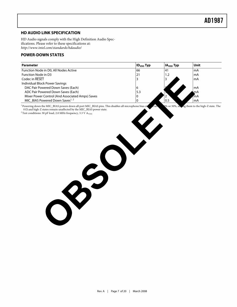
POWER-DOWN STATES
Parameter IDVDD Typ IAVDD Typ Unit
Function Node in D0, All Nodes Active 66 41 mAFunction Node in D3 21 1.2 mACodec in RESET 3 3 mAIndividual Block Power Savings DAC Pair Powered Down Saves (Each) ADC Pair Powered Down Saves (Each) Mixer Power Control (And Associated Amps) Saves MIC_BIAS Powered Down Saves1, 2
1 Powering down the MIC_BIAS powers down all port MIC_BIAS pins. This disables all microphone bias circuits set to 100% or 50%, setting them to the high-Z state. The 0 Ω and high-Z states remain unaffected by the MIC_BIAS power state.
2 Test conditions: 30 pF load, 2.0 MHz frequency, 3.3 V AVDD.
65.300
53.220.5
mAmAmAmA
OBSOLETE

Rev. A | Page 8 of 20 | March 2008
AD1987
ABSOLUTE MAXIMUM RATINGS
Stresses greater than those listed below may cause permanent damage to the device. This is a stress rating only; functional operation of the device at these or any other conditions above those indicated in the operational section of this specification is not implied. Exposure to absolute maximum rating conditions for extended periods may affect device reliability.
ESD SENSITIVITY
ENVIRONMENTAL CONDITIONS
Ambient Temperature RatingTAMB = TCASE – (PD × θCA)TCASE = Case Temperature in °CPD = Power Dissipation in WθCA = Thermal Resistance (Case-to-Ambient)θJA = Thermal Resistance (Junction-to-Ambient)θJC = Thermal Resistance (Junction-to-Case)All measurements per EIA-JESD51 with 2S2P test board per EIA-JESD51-7.
Power Supplies Rating
Digital (DVDD) –0.30 V to +3.65 VDigital I/O (DVIO) –0.30 V to +3.65 VAnalog (AVDD) –0.30 V to +3.65 VInput Current (except supply pins) ±10.0 mAAnalog Input Voltage (Signal Pins) –0.30 V to AVDD +0.3 VDigital Input Voltage (Signal Pins) –0.30 V to DVIO +0.3 VAmbient Temperature (Operating) 0°C to +70°CStorage Temperature –65°C to +150°C
ESD (electrostatic discharge) sensitive device.Charged devices and circuit boards can discharge without detection. Although this product features patented or proprietary protection circuitry, damage may occur on devices subjected to high energy ESD. Therefore, proper ESD precautions should be taken to avoid performance degradation or loss of functionality.
Table 4. Thermal Resistance
Package θJA θJC θCA Unit
LFCSP_VQ 97 15 32 °C/W
OBSOLETE
AD1987
Rev. A | Page 9 of 20 | March 2008
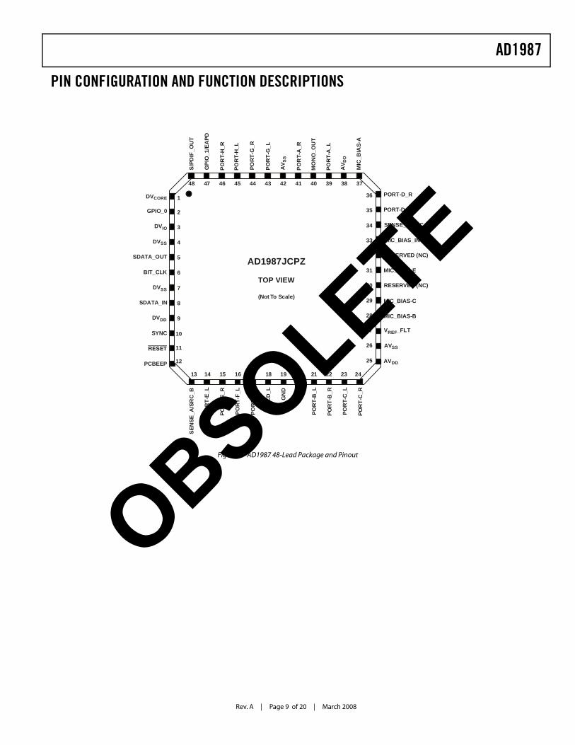
PIN CONFIGURATION AND FUNCTION DESCRIPTIONS
Figure 2. AD1987 48-Lead Package and Pinout
1
2
3
4
5
6
7
8
9
10
11
12
242313 14 15 16 17 18 19 20 21 22
34
33
36
35
25
26
27
28
29
30
31
32
44 434748 4546 373839404142
AD1987JCPZ
TOP VIEW
(Not To Scale)
DVCORE
GPIO_0
DVSS
SDATA_OUT
BIT_CLK
DVSS
SDATA_IN
DVDD
SYNC
RESET
PCBEEP
PORT-D_R
PORT-D_L
PO
RT
-C_R
PO
RT
-C_L
PO
RT
-B_R
PO
RT
-E_L
PO
RT
-F_R
PO
RT
-F_L
PO
RT
-B_L
PO
RT
-E_R
CD
_L
CD
_R
CD
_GN
D
SE
NS
E_A
/SR
C_B
SENSE_B/SRC_A
PO
RT
-A_L
MO
NO
_OU
T
GP
IO_1
/EA
PD
AV
DD
PO
RT
-H_R
PO
RT
-A_R
AV
SS
S/P
DIF
_OU
T
MIC
_BIA
S-A
MIC_BIAS_IN
MIC_BIAS-B
MIC_BIAS-C
MIC_BIAS-E
AVDD
AVSS
VREF_FLT
PO
RT
-G_L
PO
RT
-G_R
PO
RT
-H_L
RESERVED (NC)
RESERVED (NC)
DVIO
OBSOLETE

Rev. A | Page 10 of 20 | March 2008
AD1987
Table 5. AD1987 Pin Descriptions
Mnemonic Pin No. Function Description
DIGITAL INTERFACE SDATA_OUT BIT_CLK SDATA_IN SYNC RESET
5 6 8 10 11
II I/OII
Link Serial Data Output. Clocked on both edges of BIT_CLK.Link Bit Clock. 24.000 MHz serial data clock. Link Serial Data Input. AD1987 output stream clocked only on one edge of BIT_CLK.Link Frame Sync.Link Reset. Master hardware reset.
DIGITAL I/O GPIO_0 GPIO_1/EAPD
S/PDIF_OUT
2 47
48
I/OI/O
O
General-Purpose Input/Output Pin. Digital signal used to control external circuitry.General-Purpose Input/Output Pin/EAPD Pin. Digital signal used to control external circuitry. By default pin is in a high-Z state. When used as EAPD: high-Z = amp on, DVSS = amp off.S/PDIF_OUT. Supports S/PDIF output.
JACK SENSE SENSE_A/SRC_B SENSE_B/SRC_A
13 34
I/OI/O
JACK Sense A-D Input/Sense B Drive.JACK Sense E-H Input/Sense A Drive.
ANALOG I/O PCBEEP PORT-E_L PORT-E_R PORT-F_L PORT-F_R CD_L CD_GND
CD_R PORT-B_L PORT-B_R PORT-C_L PORT-C_R PORT-D_L PORT-D_R PORT-A_L MONO_OUT PORT-A_R PORT-G_L PORT-G_R PORT-H_L PORT-H_R
12 14 15 16 17 1819 2021 22 23 24 35 36 39 404143444546
LI LI, MIC, LO, SWAP LI, MIC, LO, SWAPLOLOLI LI
LILI, MIC, HP, LOLI, MIC, HP, LOLI, MIC, LOLI, MIC, LOLI, HP, LO LI, HP, LOLI, MIC, HP, LO LOLI, MIC, HP, LOLO, SWAPLO, SWAPLOLO
Monaural Input From System for Analog PCBeep.Auxiliary Input/Output Left Channel.Auxiliary Input/Output Right Channel. Auxiliary Input/Output Left Channel. Auxiliary Input/Output Right Channel. CD Audio Left Channel.CD-Audio-Analog-Ground-Reference (for Differential CD Input). Must be connected to AGND via 0.1 μF capacitor if not in use as CD_GND.CD Audio Right Channel.Front Panel Stereo MIC/Line-In. Front Panel Stereo MIC/Line-In.Rear Panel Stereo MIC/Line-In.Rear Panel Stereo MIC/Line-In. Rear Panel Headphone/Line-Out. Rear Panel Headphone/Line-Out. Front Panel Headphone/Line-Out.Monaural Output to Internal Speaker or Telephony Subsystem Speakerphone. Front Panel Headphone/Line-Out. Rear Panel C/LFE Output.Rear Panel C/LFE Output. Rear Panel Surround Center/Side. Rear Panel Surround Center/Side.
FILTER/REFERENCE MIC_BIAS-B MIC_BIAS-C MIC_BIAS-E VREF_FLT MIC_BIAS-A
DVCORE
28 29312737
1
O O O OO
O
Switchable Microphone Bias. For use with Port B (Pins 21, 22).Switchable Microphone Bias. For use with Port C (Pins 23, 24).Switchable Microphone Bias. For use with Port E (Pins 14, 15).Voltage Reference Filter.Switchable Microphone Bias. For use with Port A (Pins 39, 41)All MIC_BIAS pins are capable of: High-Z, 0 V, 1.65 V, 3.78 V, and 3.95 V (with 5.0 V on Pin 33) High-Z, 0 V, 1.65 V, 2.86 V, and 3.00 V (with 3.3 V on Pin 33).CAUTION: DO NOT APPLY 3.3 V TO THIS PIN!Filter connection for internal core voltage regulator.This pin must be connected to filter caps: 10 μF, 1.0 μF, and 0.1 μF connected in parallel between Pin 1 and DVSS (Pin 4).
The symbols used in this table are defined as: I = Input, O = Output, LI = Line level input, LO = Line level output, HP = Output capable of driving headphone load, MIC = Input supports microphones with MIC bias and boost amplifier, SWAP = Outputs can swap L/R channels (typically used to support C/LFE or shared C/LFE function).
OBSOLETE
AD1987
Rev. A | Page 11 of 20 | March 2008
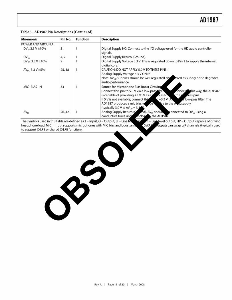
POWER AND GROUND DVIO 3.3 V ±10% 3 I Digital Supply I/O. Connect to the I/O voltage used for the HD audio controller
signals. DVSS 4, 7 I Digital Supply Return (Ground). DVDD 3.3 V ±10% 9 I Digital Supply Voltage 3.3 V. This is regulated down to Pin 1 to supply the internal
digital core. AVDD 3.3 V ±5% 25, 38 I CAUTION: DO NOT APPLY 5.0 V TO THESE PINS!
Analog Supply Voltage 3.3 V ONLY.Note: AVDD supplies should be well regulated and filtered as supply noise degrades audio performance.
MIC_BIAS_IN 33 I Source for Microphone Bias Boost Circuitry. Connect this pin to 5.0 V via a low-pass filter. When connected this way, the AD1987 is capable of providing +3.95 V as a mic bias to all of the mic bias pins. If 5 V is not available, connect this pin to +3.3 V (AVDD) via a low-pass filter. The AD1987 produces a mic bias voltage relative to the AVDD supply (typically 3.0 V @ AVDD = 3.3 V).
AVSS 26, 42 I Analog Supply Return (Ground). AVSS should be connected to DVSS using a conductive trace under, or close to, the AD1987.
Table 5. AD1987 Pin Descriptions (Continued)
Mnemonic Pin No. Function Description
The symbols used in this table are defined as: I = Input, O = Output, LI = Line level input, LO = Line level output, HP = Output capable of driving headphone load, MIC = Input supports microphones with MIC bias and boost amplifier, SWAP = Outputs can swap L/R channels (typically used to support C/LFE or shared C/LFE function).
OBSOLETE

Rev. A | Page 12 of 20 | March 2008
AD1987
HD AUDIO WIDGETSIn the following table, node IDs that are not shown are reserved for future use.
Node ID Name Type ID Type Description
00 ROOT x Root Device identification01 FUNCTION x Function Designates this device as an audio codec02 S/PDIF DAC 0 Audio Output S/PDIF digital stream output interface03 DAC_0 0 Audio Output Headphone/surround side (7.1) channel digital/audio converters04 DAC_1 0 Audio Output Stereo front channel digital/audio converters05 DAC_2 0 Audio Output Stereo C/LFE channel digital/audio converters06 DAC_3 0 Audio Output Stereo surround-back (5.1) channel digital/audio converters08 ADC_0 1 Audio Input Stereo record Channel 1 audio/digital converters09 ADC_1 1 Audio Input Stereo record Channel 2 audio/digital converters0B S/PDIF Mix Selector 3 Audio Selector Selects which ADC drives the S/PDIF mixer0C ADC Selector 0 3 Audio Selector Selects and amplifies/attenuates the input to ADC_00D ADC Selector 1 3 Audio Selector Selects and amplifies/attenuates the input to ADC_110 Digital Beep 7 Beep Generator Internal digital PCBeep signal11 Port A (Headphone) 4 Pin Complex Front panel headphone/microphone jack12 Port D (Front L/R) 4 Pin Complex Rear panel front/headphone jack13 Mono Out 4 Pin Complex Monaural output pin (internal speakers or telephony system)14 Port B (Front Mic) 4 Pin Complex Front panel microphone/headphone jack15 Port C (Line In) 4 Pin Complex Rear panel line-in jack16 Port F (Surr Back) 4 Pin Complex Rear panel surround-rear (5.1) jack17 Port E (Rear Mic) 4 Pin Complex Rear panel mic jack18 CD In 4 Pin Complex Analog CD input19 Mixer Power Down 5 Power Widget Powers down the analog mixer and associated amps1A Analog PCBeep 4 Pin Complex External analog PCBeep signal input1B S/PDIF Out 4 Pin Complex S/PDIF output pin1D S/PDIF Mixer 2 Audio Mixer Mixes the selected ADC with the digital stream to drive S/PDIF out1E Mono Out Mixer 2 Audio Mixer Selects which source drives the mono out signal20 Analog Mixer 2 Audio Mixer Mixes individually gainable analog inputs21 Mixer Output Atten 3 Audio Selector Attenuates the mixer output to drive the port mixers22 Port A Mixer 2 Audio Mixer Mixes the Port A Selected DAC and mixer output amps to drive Port A23 VREF Power Down F Vendor Defined Powers down the internal and external VREF circuitry24 Port G (C/LFE) 4 Pin Complex Rear panel C/LFE jack25 Port H (Surr Side) 4 Pin Complex Rear panel surround-side (7.1) jack26 Port E Mixer 2 Audio Mixer Mixes DAC_2 and mixer output amps to drive Port E27 Port G Mixer 2 Audio Mixer Mixes DAC_2 and mixer output amps to drive Port G28 Port H Mixer 2 Audio Mixer Mixes DAC_0 and mixer output amps to drive Port H29 Port D Mixer 2 Audio Mixer Mixes DAC_1 and mixer output amps to drive Port D2A Port F Mixer 2 Audio Mixer Mixes DAC_3 and mixer output amps to drive Port F2B Port B Mixer 2 Audio Mixer Mixes the Port B selected DAC and mixer output amps to drive Port B2C Port C Mixer 2 Audio Mixer Mixes the Port C selected DAC and mixer output amps to drive Port C2D Stereo Mix Down 2 Audio Mixer Mixes the stereo L/R channels to drive mono output2F BIAS Power Down F Vendor Defined Powers down the internal MIC_BIAS_FILT and all MIC_BIAS Pins30 Port B Out Selector 3 Audio Selector Selects the Port B DAC (0, 1)31 Port C Out Selector 3 Audio Selector Selects the Port C DAC (0, 3)37 Port A Out Selector 3 Audio Selector Selects the Port A DAC (0, 1)38 Port A Boost 3 Audio Selector Microphone boost amp for Port A39 Port B Boost 3 Audio Selector Microphone boost amp for Port B3A Port C Boost 3 Audio Selector Microphone boost amp for Port C3C Port E Boost 3 Audio Selector Microphone boost amp for Port E
OBSOLETE

AD1987
Rev. A | Page 13 of 20 | March 2008
HD AUDIO PARAMETERSTable 6. Root and Function Node Parameters
Node ID Name Vendor ID 00 01 Revision ID 021
1 Subject to change with silicon stepping.
03Sub Node Count 04
Func. Group Type 05
Audio F.G. Caps 08 GPIO Caps 11
00 ROOT 11D41987 00100200 0001000101 FUNCTION 0002003B 00000001 00010C0C 40000002
Table 7. SubSystem ID1
1 The default SSID is overwritten by platform BIOS after power-on. It is preserved across HD Audio link reset and verb reset.
SubSystem ID 31:16 15:8 7:0Node ID Name Value SSID SKU Asm ID01 FUNCTION BFD40000 BFD7 00 00
OBSOLETE

Rev. A | Page 14 of 20 | March 2008
AD1987
WIDGET PARAMETERSTable 8. Widget Parameters
Node ID
Widget Capabilities 09
PCM Size, Rate 0A
Stream Formats 0B
Pin Capabilities 0C
Input Amp Capabilities 0D
ConnList Length 0E
Power States 0F
Processing Capabilities 10
Output Amp Capabilities 12
Volume Knob Capabilities 13
01 00000480 000E01FF 00000001 80000000 00000009 0005272702 00030311 000E01E0 00000005 0000000103 00000405 000E01FF 00000001 00000000 00000009 0005272704 00000405 000E01FF 00000001 00000000 00000009 0005272705 00000405 000E01FF 00000001 00000000 00000009 0005272706 00000405 000E01FF 00000001 00000000 00000009 0005272708 00100501 000E01FF 00000001 00000001 0000000909 00100501 000E01FF 00000001 00000001 000000090B 00300301 000000020C 0030010D 00000008 800536270D 0030010D 00000008 8005362710 0070000C 00000000 800B0F0F11 0040018D 0000373F 00000001 8000000012 0040058D 0001003F 00000001 00000009 8000000013 0040050C 00010010 00000001 00000009 80051F1F14 0040018D 0000373F 00000001 8000000015 0040018D 00003737 00000001 8000000016 0040018D 00000017 00000001 8000000017 0040098D 00003737 00000001 8000000018 00400001 00000020 0000000019 00500500 00000002 000000091A 00400000 00000020 000000001B 0040030D 00000010 00000001 800527271D 00200303 80000000 000000021E 00200103 80000000 0000000220 0020010B 80051F17 0000000821 0030010D 00000001 80051F1F22 00200103 80000000 0000000223 00F00100 0000000824 0040098D 00000017 00000001 8000000025 0040018D 00000017 00000001 8000000026 00200103 80000000 0000000227 00200103 80000000 0000000228 00200103 80000000 0000000229 00200103 80000000 000000022A 00200103 80000000 000000022B 00200103 80000000 000000022C 00200103 80000000 000000022D 00200100 000000012F 00F00100 0000000430 00300101 0000000231 00300101 0000000237 00300101 0000000238 0030010D 00000001 0027030039 0030010D 00000001 002703003A 0030010D 00000001 002703003C 0030010D 00000001 00270300
OBSOLETE

AD1987
Rev. A | Page 15 of 20 | March 2008
CONNECTION LISTTable 9. Connection List
Node ID
Connections 0 1 2 3 4 5 6 7
[0–3] [4–7] NID I NID I NID I NID I NID I NID I NID I NID
02 0000001D 1D0304050608 0000000C 0C09 0000000D 0D0B 00000908 08 090C 18BC3938 20123B3B 38 39 1 3C 18 3B 3B 12 200D 18BC3938 20123B3B 38 39 1 3C 18 3B 3B 12 201011 00000022 2212 00000029 2913 0000002D 2D14 0000002B 2B15 0000002C 2C16 0000002A 2A17 00000026 261819 00002120 20 211A1B 00000002 021D 00000B01 01 0B1E 00002104 04 2120 12383A39 1A183B3C 39 3A 38 12 3C 3B 18 1A21 00000020 2022 00002137 37 2123 A2209811 BC30AE24 11 1 18 20 1 22 24 1 2E 30 1 3C24 00000027 2725 00000028 2826 00002105 05 2127 00002105 05 2128 00002103 03 2129 00002104 04 212A 00002106 06 212B 00002130 30 212C 00002131 31 212D 0000001E 1E2F 11171514 14 15 17 1130 00000403 03 0431 00000603 03 0637 00000403 03 0438 00000011 1139 00000014 143A 00000015 153C 00000017 17
OBSOLETE

Rev. A | Page 16 of 20 | March 2008
AD1987
DEFAULT CONFIGURATION BYTESIn Table 10, default configuration values are set on codec power-up only. Default configuration values are not reset by link or soft reset to preserve modifications by BIOS control.
Table 10. Default Configuration Bytes
31:30 29:28 27:24 23:20 19:16 15:12 8 7:4 3:0
Connectivity
Location
Def. Device Conn Type Color Def Assn SequenceName Value Chasis Position JD OR
Port A (Headphone) 0221401F Jack External Front HP Out 1/8” Jack Green 0 1 FPort D (Line Out) 01014010 Jack External Rear Line Out 1/8” Jack Green 0 1 0Mono Out 991301F0 Fixed Internal Special 3 Speaker ATAPI Unknown 1 F 0Port B (Front Mic) 02A190F0 Jack External Front Mic In 1/8” Jack Pink 0 F 0Port C (Line In) 01813021 Jack External Rear Line In 1/8” Jack Blue 0 2 1Port F (Surr Back) 01011012 Jack External Rear Line Out 1/8” Jack Black 0 1 2Port E (Rear Mic) 01A19020 Jack External Rear Mic In 1/8” Jack Pink 0 2 0CD IN 9933012E Fixed Internal Special 3 CD ATAPI Unknown 1 2 EAnalog PCBeep 99F301F0 Fixed Internal Special 3 Other ATAPI Unknown 1 F 0S/PDIF Out 014511F0 Jack External Rear SPDIF Out Optical Black 1 F 0Port G (C/LFE) 01016011 Jack External Rear Line Out 1/8” Jack Orange 0 1 1Port H (Surr Side) 01012014 Jack External Rear Line Out 1/8” Jack Grey 0 1 4
OBSOLETE

AD1987
Rev. A | Page 17 of 20 | March 2008
OUTLINE DIMENSIONSDimensions are shown in millimeters.
ORDERING GUIDE
Figure 3. 48-Lead, Lead Frame Chip Scale Package [LFCSP_VQ] 7 mm × 7 mm Body, Very Thin Quad
(CP-48-1)
Model Temperature Range Package Description Package Option
AD1987JCPZ1
1 Z = RoHS Compliant Part.
0°C to 70°C 48-Lead LFCSP_VQ CP-48-1AD1987JCPZ-RL1 0°C to 70°C 48-Lead LFCSP_VQ, 13” Tape and Reel CP-48-1
PIN 1INDICATOR
TOPVIEW
6.75BSC SQ
7.00BSC SQ
148
1213
3736
2425
5.25
5.10 SQ
4.95
0.50
0.40
0.30
0.30
0.23
0.18
0.50 BSC
12° MAX
0.20 REF
0.80 MAX
0.65 TYP1.00
0.85
0.80
5.50REF
0.05 MAX
0.02 NOM
0.60 MAX
0.60 MAX PIN 1INDICATOR
COPLANARITY0.08
SEATINGPLANE
0.25 MIN
EXPOSEDPAD
(BOTTOM VIEW)
COMPLIANT TO JEDEC STANDARDS MO-220-VKKD-2
OBSOLETE

Rev. A | Page 18 of 20 | March 2008
AD1987
OBSOLETE

AD1987
Rev. A | Page 19 of 20 | March 2008
OBSOLETE

Rev. A | Page 20 of 20 | March 2008
AD1987
©2008 Analog Devices, Inc. All rights reserved. Trademarks andregistered trademarks are the property of their respective owners.
D06536-0-3/08(A)
OBSOLETE
Related Documents