FN3142 Rev 10.00 Page 1 of 25 Jun 14, 2016 FN3142 Rev 10.00 Jun 14, 2016 HI-506, HI-507, HI-508, HI-509 Single 16 and 8/Differential 8-Channel and 4-Channel CMOS Analog Multiplexers DATASHEET The HI-506/HI-507 and HI-508/HI-509 monolithic CMOS multiplexers each include an array of sixteen and eight analog switches respectively, a digital decoder circuit for channel selection, voltage reference for logic thresholds, and an enable input for device selection when several multiplexers are present. The Dielectric Isolation (DI) process used in fabrication of these devices eliminates the problem of latchup. DI also offers much lower substrate leakage and parasitic capacitance than conventional junction isolated CMOS (see Application Note AN520). The switching threshold for each digital input is established by an internal +5V reference, providing a guaranteed minimum 2.4V for logic “1” and maximum 0.8V for logic “0”. This allows direct interface without pullup resistors to signals from most logic families: CMOS, TTL, DTL and some PMOS. For protection against transient overvoltage, the digital inputs include a series 200 resistor and diode clamp to each supply. The HI-506 is a single 16-channel, the HI-507 is an 8-channel differential, the HI-508 is a single 8-channel and the HI-509 is a 4-channel differential multiplexer. If input overvoltages are present, the HI-546/HI-547/HI-548/ HI-549 multiplexers are recommended. Features • Pb-Free Available (RoHS Compliant) (See Ordering Info) • Low ON Resistance . . . . . . . . . . . . . . . . . . . . . . . . 180 • Wide Analog Signal Range ±15V • TTL/CMOS Compatible • Access Time . . . . . . . . . . . . . . . . . . . . . . . . . . . . . 250ns • Maximum Power Supply . . . . . . . . . . . . . . . . . . . . . . 44V • Break-Before-Make Switching • No Latch-Up • Replaces DG506A/DG506AA and DG507A/DG507AA • Replaces DG508A/DG508AA and DG509A/DG509AA Applications • Data Acquisition Systems • Precision Instrumentation • Demultiplexing • Selector Switch

Welcome message from author
This document is posted to help you gain knowledge. Please leave a comment to let me know what you think about it! Share it to your friends and learn new things together.
Transcript
FN3142Rev 10.00
Jun 14, 2016
HI-506, HI-507, HI-508, HI-509Single 16 and 8/Differential 8-Channel and 4-Channel CMOS Analog Multiplexers
DATASHEET
The HI-506/HI-507 and HI-508/HI-509 monolithic CMOS multiplexers each include an array of sixteen and eight analog switches respectively, a digital decoder circuit for channel selection, voltage reference for logic thresholds, and an enable input for device selection when several multiplexers are present. The Dielectric Isolation (DI) process used in fabrication of these devices eliminates the problem of latchup. DI also offers much lower substrate leakage and parasitic capacitance than conventional junction isolated CMOS (see Application Note AN520).
The switching threshold for each digital input is established by an internal +5V reference, providing a guaranteed minimum 2.4V for logic “1” and maximum 0.8V for logic “0”. This allows direct interface without pullup resistors to signals from most logic families: CMOS, TTL, DTL and some PMOS. For protection against transient overvoltage, the digital inputs include a series 200 resistor and diode clamp to each supply.
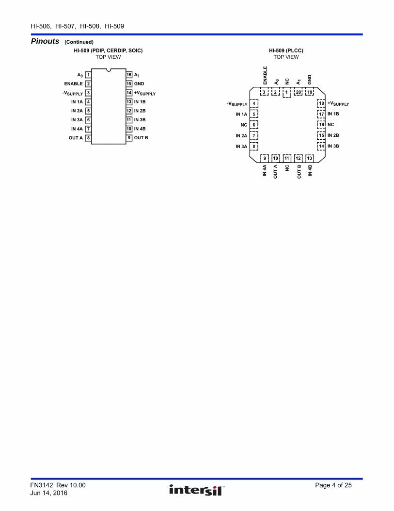
The HI-506 is a single 16-channel, the HI-507 is an 8-channel differential, the HI-508 is a single 8-channel and the HI-509 is a 4-channel differential multiplexer.
If input overvoltages are present, the HI-546/HI-547/HI-548/ HI-549 multiplexers are recommended.
Features
• Pb-Free Available (RoHS Compliant) (See Ordering Info)
• Low ON Resistance . . . . . . . . . . . . . . . . . . . . . . . . 180
• Wide Analog Signal Range ±15V
• TTL/CMOS Compatible
• Access Time . . . . . . . . . . . . . . . . . . . . . . . . . . . . . 250ns
• Maximum Power Supply . . . . . . . . . . . . . . . . . . . . . . 44V
• Break-Before-Make Switching
• No Latch-Up
• Replaces DG506A/DG506AA and DG507A/DG507AA
• Replaces DG508A/DG508AA and DG509A/DG509AA
Applications
• Data Acquisition Systems
• Precision Instrumentation
• Demultiplexing
• Selector Switch
FN3142 Rev 10.00 Page 1 of 25Jun 14, 2016
HI-506, HI-507, HI-508, HI-509
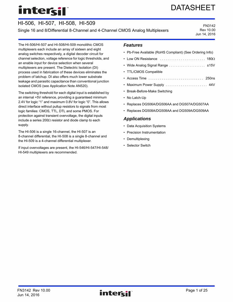
Ordering Information
PART NUMBER PART MARKINGTEMP.
RANGE (°C) PACKAGE PKG. DWG. #
HI1-0506-2 HI1-506-2 -55 to +125 28 Ld CERDIP F28.6
HI4P0506-5Z (Note 1) HI4P 506-5Z 0 to +75 28 Ld PLCC (Pb-free) N28.45
HI9P0506-9Z (Note 1) HI9P506-9Z -40 to +85 28 Ld SOIC (Pb-free) M28.3
HI3-0507-5Z (No longer available, recommended replacement: HI3-0547-5Z)
HI3-507-5Z 0 to +75 28 Ld PDIP (Note 3) (Pb-free) E28.6
HI1-0508-2 HI1-508-2 -55 to 125 16 Ld CERDIP F16.3
HI3-0508-5Z (Note 1) HI3-508-5Z 0 to +75 16 Ld PDIP (Note 3) (Pb-free) E16.3
HI9P0508-5Z (Notes 1, 2) HI9P508-5Z 0 to +75 16 Ld SOIC (Pb-free) M16.15
HI9P0508-9Z (Note 1) HI9P508-9Z -40 to +85 16 Ld SOIC (Pb-free) M16.15
HI1-0509-2 HI1-509-2 -55 to +125 16 Ld CERDIP F16.3
HI4P0509-5Z (Notes 1, 2) (No longer available, recommended replacement: DG409DYZ)
HI4P 509-5Z 0 to +75 20 Ld PLCC (Pb-free) N20.35
NOTES:
1. These Intersil Pb-free plastic packaged products employ special Pb-free material sets; molding compounds/die attach materials and 100% matte tin plate PLUS ANNEAL - e3 termination finish, which is RoHS compliant and compatible with both SnPb and Pb-free soldering operations. Intersil Pb-free products are MSL classified at Pb-free peak reflow temperatures that meet or exceed the Pb-free requirements of IPC/JEDEC J STD-020.
2. Add “96” suffix for tape and reel. Please refer to TB347 for details on reel specifications.
3. Pb-free PDIPs can be used for through hole wave solder processing only. They are not intended for use in Reflow solder processing applications.
FN3142 Rev 10.00 Page 2 of 25Jun 14, 2016

HI-506, HI-507, HI-508, HI-509
PinoutsHI-506 (CERDIP, SOIC)
TOP VIEWHI-506 (PLCC)
TOP VIEW
HI-507 (PDIP, CERDIP)TOP VIEW
HI-508 (PDIP, CERDIP, SOIC)TOP VIEW
+VSUPPLY
NC
NC
IN 16
IN 15
IN 14
IN 13
IN 12
IN 11
IN 10
IN 9
GND
NC
ADDRESS A3
OUT
IN 8
IN 7
IN 6
IN 5
IN 3
IN 1
ENABLE
ADDRESS A0
ADDRESS A1
ADDRESS A2
-VSUPPLY
IN 4
IN 2
28
27
26
25
24
23
22
21
20
19
18
17
16
15
1
2
3
4
5
6
7
8
9
10
11
12
13
14
IN 15
IN 14
IN 13
IN 12
IN 11
IN 10
IN 9
IN 1
6
NC
NC
+V
SU
PP
LY
OU
T
-VS
UP
PLY
IN 8
GN
D
NC A3
A2
A1
EN
AB
LE
A0
IN 7
IN 6
IN 5
IN 4
IN 3
IN 2
IN 111
10
5
6
7
8
9
23
24
25
22
21
20
19
14 15 16 17 1812 13
3 2 14 28 27 26
+VSUPPLY
OUT B
NC
IN 8B
IN 7B
IN 6B
IN 5B
IN 4B
IN 3B
IN 2B
IN 1B
GND
NC
NC
OUT A
IN 8A
IN 7A
IN 6A
IN 5A
IN 3A
IN 1A
ENABLE
ADDRESS A0
ADDRESS A1
ADDRESS A2
-VSUPPLY
IN 4A
IN 2A
28
27
26
25
24
23
22
21
20
19
18
17
16
15
1
2
3
4
5
6
7
8
9
10
11
12
13
14
14
15
16
9
13
12
11
10
1
2
3
4
5
7
6
8
A0
ENABLE
-VSUPPLY
IN 1
IN 2
IN 3
OUT
IN 4
A1
GND
+VSUPPLY
IN 5
IN 6
IN 7
IN 8
A2
FN3142 Rev 10.00 Page 3 of 25Jun 14, 2016
HI-506, HI-507, HI-508, HI-509
HI-509 (PDIP, CERDIP, SOIC)TOP VIEW
HI-509 (PLCC)TOP VIEW
Pinouts (Continued)
14
15
16
9
13
12
11
10
1
2
3
4
5
7
6
8
A0
ENABLE
-VSUPPLY
IN 1A
IN 2A
IN 3A
OUT A
IN 4A
A1
+VSUPPLY
IN 1B
IN 2B
IN 3B
IN 4B
OUT B
GND
-VSUPPLY
IN 1A
NC
IN 2A
IN 3A
EN
AB
LE
A0
NC
A1
GN
D
IN 4
A
OU
T A NC
OU
T B
IN 4
B
+VSUPPLY
IN 1B
NC
IN 2B
IN 3B
4
5
6
7
8
10 11 12 139
3 2 1 20 19
16
17
18
15
14
FN3142 Rev 10.00 Page 4 of 25Jun 14, 2016
HI-506, HI-507, HI-508, HI-509
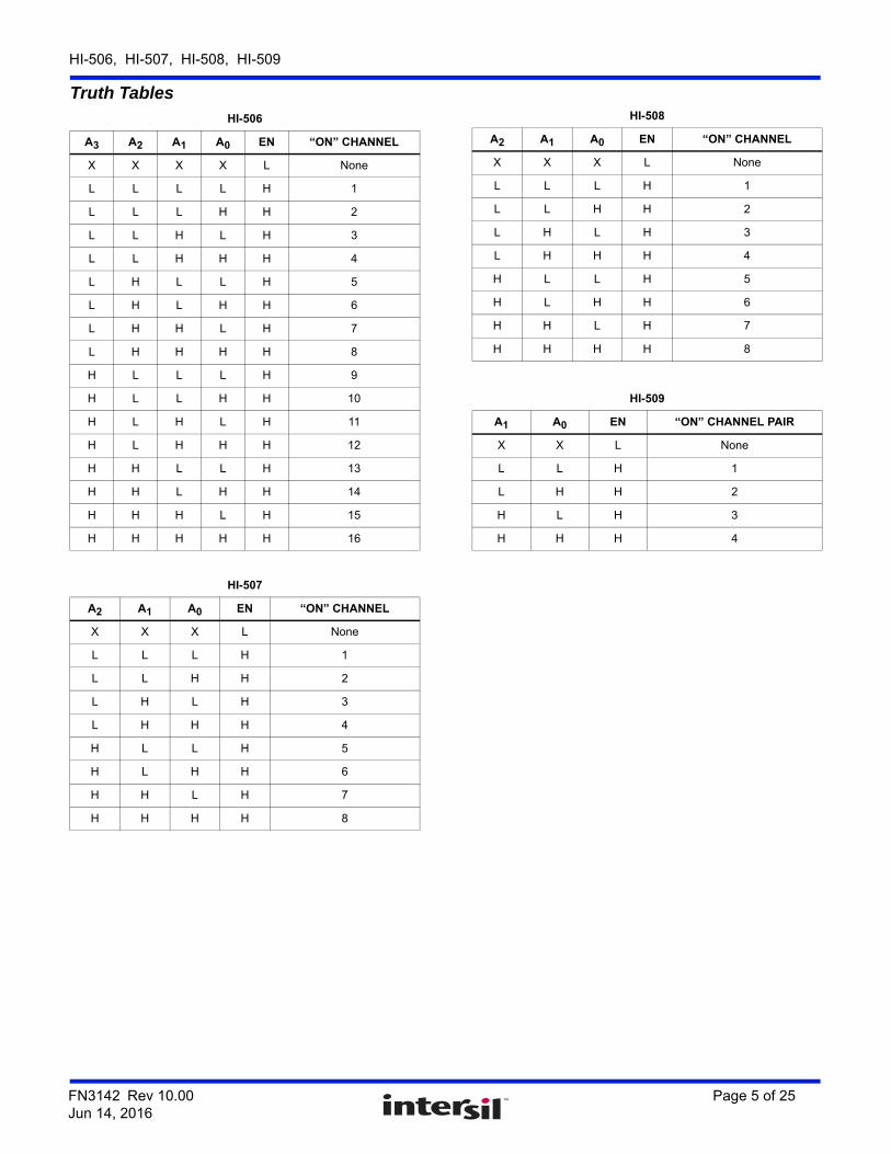
Truth TablesHI-506
A3 A2 A1 A0 EN “ON” CHANNEL
X X X X L None
L L L L H 1
L L L H H 2
L L H L H 3
L L H H H 4
L H L L H 5
L H L H H 6
L H H L H 7
L H H H H 8
H L L L H 9
H L L H H 10
H L H L H 11
H L H H H 12
H H L L H 13
H H L H H 14
H H H L H 15
H H H H H 16
HI-507
A2 A1 A0 EN “ON” CHANNEL
X X X L None
L L L H 1
L L H H 2
L H L H 3
L H H H 4
H L L H 5
H L H H 6
H H L H 7
H H H H 8
HI-508
A2 A1 A0 EN “ON” CHANNEL
X X X L None
L L L H 1
L L H H 2
L H L H 3
L H H H 4
H L L H 5
H L H H 6
H H L H 7
H H H H 8
HI-509
A1 A0 EN “ON” CHANNEL PAIR
X X L None
L L H 1
L H H 2
H L H 3
H H H 4
FN3142 Rev 10.00 Page 5 of 25Jun 14, 2016
HI-506, HI-507, HI-508, HI-509
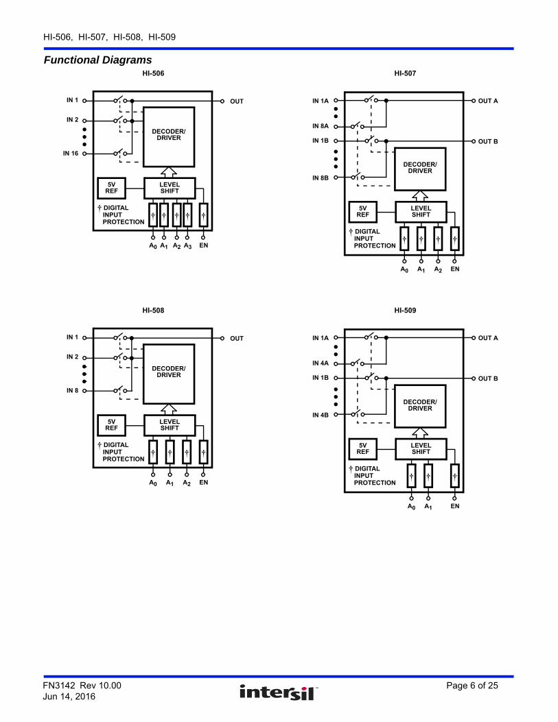
Functional DiagramsHI-506 HI-507
HI-508 HI-509
DECODER/DRIVER
† † † †
OUTIN 1
IN 2
IN 16
† DIGITAL
PROTECTION
A0 A1 A2 A3
†
EN
INPUT
LEVELSHIFT
5VREF
DECODER/DRIVER
† † †
OUT B
IN 8A
IN 1A
IN 1B
† DIGITAL
PROTECTION
A0 A1 A2
†
EN
INPUT
LEVELSHIFT
5VREF
OUT A
IN 8B
DECODER/DRIVER
† † †
OUTIN 1
IN 2
IN 8
† DIGITAL
PROTECTION
A0 A1 A2
†
EN
INPUT
LEVELSHIFT
5VREF
DECODER/DRIVER
† †
OUT B
IN 4A
IN 1A
IN 1B
† DIGITAL
PROTECTION
A0 A1
†
EN
INPUT
LEVELSHIFT
5VREF
OUT A
IN 4B
FN3142 Rev 10.00 Page 6 of 25Jun 14, 2016
HI-506, HI-507, HI-508, HI-509
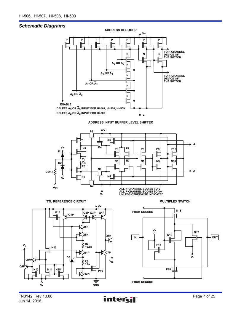
Schematic DiagramsADDRESS DECODER
ADDRESS INPUT BUFFER LEVEL SHIFTER
TTL REFERENCE CIRCUIT MULTIPLEX SWITCH
P
N
A0 OR A0
TO N-CHANNELDEVICE OFTHE SWITCH
A1 OR A1
A2 OR A2
A3 OR A3
ENABLE
P P P P P P
V+
V-
N
N
N
N
N NTO P-CHANNELDEVICE OFTHE SWITCH
DELETE A3 OR A3 INPUT FOR HI-507, HI-508, HI-509
DELETE A2 OR A2 INPUT FOR HI-509
V+
P3
D1
D2
200
AIN
VR
ALL N-CHANNEL BODIES TO V-ALL P-CHANNEL BODIES TO V+UNLESS OTHERWISE INDICATED
A
V-
P1
N1
VL
P2
N2
N3
V-
V+
P4
P5
P6 P7 P8 P9 P10
N6 N7 N8 N9 N10
N4
N5
A
VL
Q9P
Q10N
N13 N14
P15Q1P
N15
Q5N
D3
Q11P
R36.8k
P16
R216.8k
Q12N
Q6N
Q2P
V+
Q3P Q4P
N12
Q7P
V- GND
Q8N
VR
FROM DECODE
V+
N18
N19
P17
N17
V-
P18
OUT
FROM DECODE
IN
FN3142 Rev 10.00 Page 7 of 25Jun 14, 2016
HI-506, HI-507, HI-508, HI-509
Absolute Maximum Ratings Thermal Information
V+ to V- . . . . . . . . . . . . . . . . . . . . . . . . . . . . . . . . . . . . . . . . . . .+44VV+ to GND . . . . . . . . . . . . . . . . . . . . . . . . . . . . . . . . . . . . . . . . .+22VV- to GND. . . . . . . . . . . . . . . . . . . . . . . . . . . . . . . . . . . . . . . . . -25VDigital Input Voltage (VEN, VA) . . . . . (V-) -4V to (V+) +4V or 20mA,
Whichever Occurs FirstAnalog Signal (VIN, VOUT, Note 5) . . . . . . . . . . (V-) -2V to (V+) +2VContinuous Current, In or Out . . . . . . . . . . . . . . . . . . . . . . . . . 20mAPeak Current, In or Out (Pulsed 1ms, 10% Duty Cycle Max) . 40mA
Operating ConditionsTemperature Ranges
HI-50X-2 . . . . . . . . . . . . . . . . . . . . . . . . . . . . . . . .-55°C to +125°CHI-50X-4 . . . . . . . . . . . . . . . . . . . . . . . . . . . . . . . . .-25°C to +85°CHI-50X-5 . . . . . . . . . . . . . . . . . . . . . . . . . . . . . . . . . . 0°C to +75°CHI-50X-9 . . . . . . . . . . . . . . . . . . . . . . . . . . . . . . . . .-40°C to +85°C
Typical Minimum Supply Voltage . . . . . . . . . . . . 10V or Single 20V
Thermal Resistance (Typical, Note 4) JA (°C/W) JC (°C/W)
16 Ld CERDIP Package. . . . . . . . . . . . 85 3216 Ld SOIC Package . . . . . . . . . . . . . . 115 N/A16 Ld PDIP Package . . . . . . . . . . . . . . 100 N/A20 Ld PLCC Package. . . . . . . . . . . . . . 80 N/A28 Ld CERDIP Package. . . . . . . . . . . . 55 1828 Ld PDIP Package . . . . . . . . . . . . . . 60 N/A28 Ld SOIC Package . . . . . . . . . . . . . . 70 N/A28 Ld PLCC Package. . . . . . . . . . . . . . 70 N/A
Maximum Junction TemperatureCeramic Packages . . . . . . . . . . . . . . . . . . . . . . . . . . . . . . . +175°CPlastic Packages . . . . . . . . . . . . . . . . . . . . . . . . . . . . . . . . +150°C
Maximum Storage Temperature Range . . . . . . . . . . -65°C to +150°CPb-free reflow profile . . . . . . . . . . . . . . . . . . . . . . . . . .see link below
http://www.intersil.com/pbfree/Pb-FreeReflow.asp
CAUTION: Do not operate at or near the maximum ratings listed for extended periods of time. Exposure to such conditions may adversely impact product reliability andresult in failures not covered by warranty.
NOTE:
4. JA is measured with the component mounted on a low effective thermal conductivity test board in free air. See Tech Brief TB379 for details.
5. Signals on IN or OUT exceeding V+ or V- are clamped by internal diodes. Limit resulting current to maximum current ratings. If an overvoltage condition is anticipated (analog input exceeds either power supply voltage), the Intersil HI-546/HI-547/HI-548/HI-549 multiplexers are recommended.
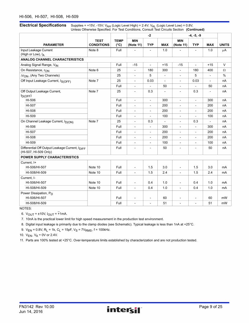
Electrical Specifications Supplies = +15V, -15V; VAH (Logic Level High) = 2.4V; VAL (Logic Level Low) = 0.8V,Unless Otherwise Specified. For Test Conditions, Consult Test Circuits Section
PARAMETERTEST
CONDITIONSTEMP(°C)
-2 -4, -5, -9
UNITSMIN
(Note 11) TYP MAXMIN
(Note 11) TYP MAX
DYNAMIC CHARACTERISTICS
Access Time, tA 25 - 250 500 - 250 - ns
Full - - 1000 - - 1000 ns
Break-Before-Make Delay, tOPEN 25 25 80 - 25 80 - ns
Enable Delay (ON), tON(EN) 25 - 250 500 - 250 - ns
Full - - 1000 - - 1000 ns
Enable Delay (OFF), tOFF(EN) 25 - 250 500 - 250 - ns
Full - - 1000 - - 1000 ns
Settling Time, tS(HI-506 and HI-507)
To 0.1% 25 - 1.2 - - 1.2 - s
To 0.01% 25 - 2.4 - - 2.4 - s
Settling Time, tS(HI-508 and HI-509)
To 0.1% 25 - 360 - - 360 - ns
To 0.01% 25 - 600 - - 600 - ns
Off Isolation Note 9 25 - 68 - - 68 - dB
Channel Input Capacitance, CS(OFF) 25 - 10 - - 10 - pF
Channel Output Capacitance, CD(OFF)HI-506 25 - 52 - - 52 - pF
HI-507 25 - 30 - - 30 - pF
HI-508 25 - 17 - - 17 - pF
HI-509 25 - 12 - - 12 - pF
Digital Input Capacitance, CA 25 - 6 - - 6 - pF
Input to Output Capacitance, CDS(OFF) 25 - 0.08 - - 0.08 - pF
DIGITAL INPUT CHARACTERISTICS
Input Low Threshold, VAL Full - - 0.8 - - 0.8 V
Input High Threshold, VAH Full 2.4 - - 2.4 - - V
FN3142 Rev 10.00 Page 8 of 25Jun 14, 2016
HI-506, HI-507, HI-508, HI-509
Input Leakage Current(High or Low), IA
Note 8 Full - - 1.0 - - 1.0 A
ANALOG CHANNEL CHARACTERISTICS
Analog Signal Range, VIN Full -15 - +15 -15 - +15 V
On Resistance, rON Note 6 25 - 180 300 - 180 400
rON, (Any Two Channels) 25 - 5 - - 5 - %
Off Input Leakage Current, IS(OFF) Note 7 25 - 0.03 - - 0.03 - nA
Full - - 50 - - 50 nA
Off Output Leakage Current,ID(OFF)
Note 7 25 - 0.3 - - 0.3 - nA
HI-506 Full - - 300 - - 300 nA
HI-507 Full - - 200 - - 200 nA
HI-508 Full - - 200 - - 200 nA
HI-509 Full - - 100 - - 100 nA
On Channel Leakage Current, ID(ON) Note 7 25 - 0.3 - - 0.3 - nA
HI-506 Full - - 300 - - 300 nA
HI-507 Full - - 200 - - 200 nA
HI-508 Full - - 200 - - 200 nA
HI-509 Full - - 100 - - 100 nA
Differential Off Output Leakage Current, IDIFF (HI-507, HI-509 Only)
Full - - 50 - - 50 nA
POWER SUPPLY CHARACTERISTICS
Current, I+
HI-506/HI-507 Note 10 Full - 1.5 3.0 - 1.5 3.0 mA
HI-508/HI-509 Note 10 Full - 1.5 2.4 - 1.5 2.4 mA
Current, I-
HI-506/HI-507 Note 10 Full - 0.4 1.0 - 0.4 1.0 mA
HI-508/HI-509 Note 10 Full - 0.4 1.0 - 0.4 1.0 mA
Power Dissipation, PDHI-506/HI-507 Full - - 60 - - 60 mW
HI-508/HI-509 Full - - 51 - - 51 mW
NOTES:
6. VOUT = ±10V, IOUT = +1mA.
7. 10nA is the practical lower limit for high speed measurement in the production test environment.
8. Digital input leakage is primarily due to the clamp diodes (see Schematic). Typical leakage is less than 1nA at +25°C.
9. VEN = 0.8V, RL = 1k, CL = 15pF, VS = 7VRMS, f = 100kHz.
10. VEN, VA = 0V or 2.4V.
11. Parts are 100% tested at +25°C. Over-temperature limits established by characterization and are not production tested.
Electrical Specifications Supplies = +15V, -15V; VAH (Logic Level High) = 2.4V; VAL (Logic Level Low) = 0.8V,Unless Otherwise Specified. For Test Conditions, Consult Test Circuits Section (Continued)
PARAMETERTEST
CONDITIONSTEMP(°C)
-2 -4, -5, -9
UNITSMIN
(Note 11) TYP MAXMIN
(Note 11) TYP MAX
FN3142 Rev 10.00 Page 9 of 25Jun 14, 2016
HI-506, HI-507, HI-508, HI-509
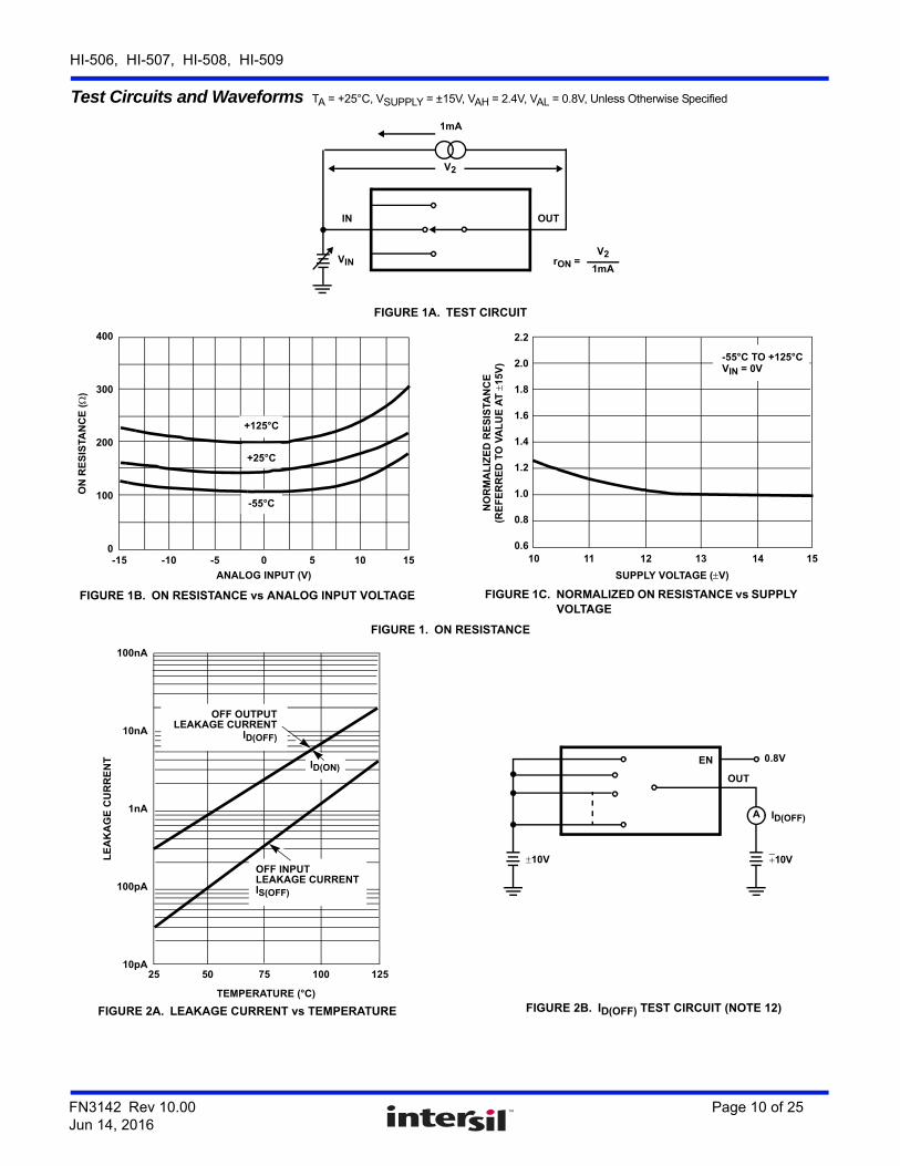
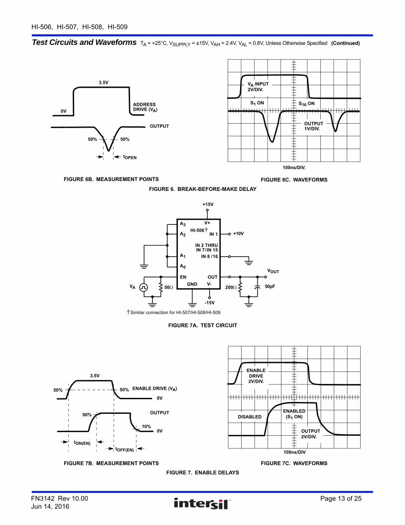
Test Circuits and Waveforms TA = +25°C, VSUPPLY = ±15V, VAH = 2.4V, VAL = 0.8V, Unless Otherwise Specified
FIGURE 1A. TEST CIRCUIT
FIGURE 1B. ON RESISTANCE vs ANALOG INPUT VOLTAGE FIGURE 1C. NORMALIZED ON RESISTANCE vs SUPPLY VOLTAGE
FIGURE 1. ON RESISTANCE
FIGURE 2A. LEAKAGE CURRENT vs TEMPERATURE FIGURE 2B. ID(OFF) TEST CIRCUIT (NOTE 12)
1mA
OUTIN
VIN rON =V2
1mA
V2
400
300
200
100
0-15
ANALOG INPUT (V)
ON
RE
SIS
TAN
CE
(
)
-10 -5 0 5 10 15
+125°C
+25°C
-55°C
2.2
2.0
1.8
1.6
1.4
1.2
1.0
0.8
0.6
NO
RM
AL
IZE
D R
ES
ISTA
NC
E(R
EF
ER
RE
D T
O V
AL
UE
AT
15
V)
10 11 12 13 14 15
SUPPLY VOLTAGE (V)
-55°C TO +125°CVIN = 0V
100nA
10nA
1nA
100pA
10pA
LE
AK
AG
E C
UR
RE
NT
25 50 75 100 125
TEMPERATURE (°C)
OFF OUTPUTLEAKAGE CURRENT
ID(OFF)
ID(ON)
OFF INPUTLEAKAGE CURRENTIS(OFF)
A
10V10V
0.8VEN
OUT
ID(OFF)
FN3142 Rev 10.00 Page 10 of 25Jun 14, 2016
HI-506, HI-507, HI-508, HI-509
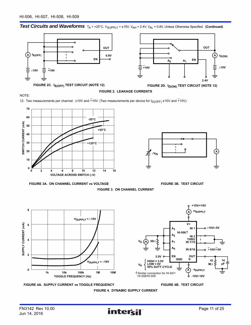
FIGURE 2C. IS(OFF) TEST CIRCUIT (NOTE 12) FIGURE 2D. ID(ON) TEST CIRCUIT (NOTE 12)
FIGURE 2. LEAKAGE CURRENTSNOTE:
12. Two measurements per channel: ±10V and +10V. (Two measurements per device for ID(OFF) ±10V and +10V)
FIGURE 3A. ON CHANNEL CURRENT vs VOLTAGE FIGURE 3B. TEST CIRCUIT
FIGURE 3. ON CHANNEL CURRENT
FIGURE 4A. SUPPLY CURRENT vs TOGGLE FREQUENCY FIGURE 4B. TEST CIRCUIT
FIGURE 4. DYNAMIC SUPPLY CURRENT
Test Circuits and Waveforms TA = +25°C, VSUPPLY = ±15V, VAH = 2.4V, VAL = 0.8V, Unless Otherwise Specified (Continued)
+10V10V
0.8VEN
A
OUT
IS(OFF)
OUT
ID(ON)A
+10V 10V
2.4V
ENA0 A1
70
60
50
40
30
20
10
00 2 4 6 8 10 12 14 16
VOLTAGE ACROSS SWITCH (V)
SW
ITC
H C
UR
RE
NT
(m
A)
-55°C
+25°C
+125°C
AVIN
8
6
4
2
01k
TOGGLE FREQUENCY (Hz)
SU
PP
LY C
UR
RE
NT
(m
A)
10k 100k 1M 10M
VSUPPLY = 15V
VSUPPLY = 10V
10V/5V
+15V/+10V
V+
V-
IN 1
IN 2
IN 8/16
OUT
A0
EN
A1
10 14M pF
A3
A2
50VA
3.5VGND
A
-15V/-10V
A -ISUPPLY
+ISUPPLY
+10V/+5V
VA
HIGH = 3.5VLOW = 0V50% DUTY CYCLE
THRUIN 7/15
HI-506†
†Similar connection for HI-507/HI-508/HI-509
FN3142 Rev 10.00 Page 11 of 25Jun 14, 2016
HI-506, HI-507, HI-508, HI-509
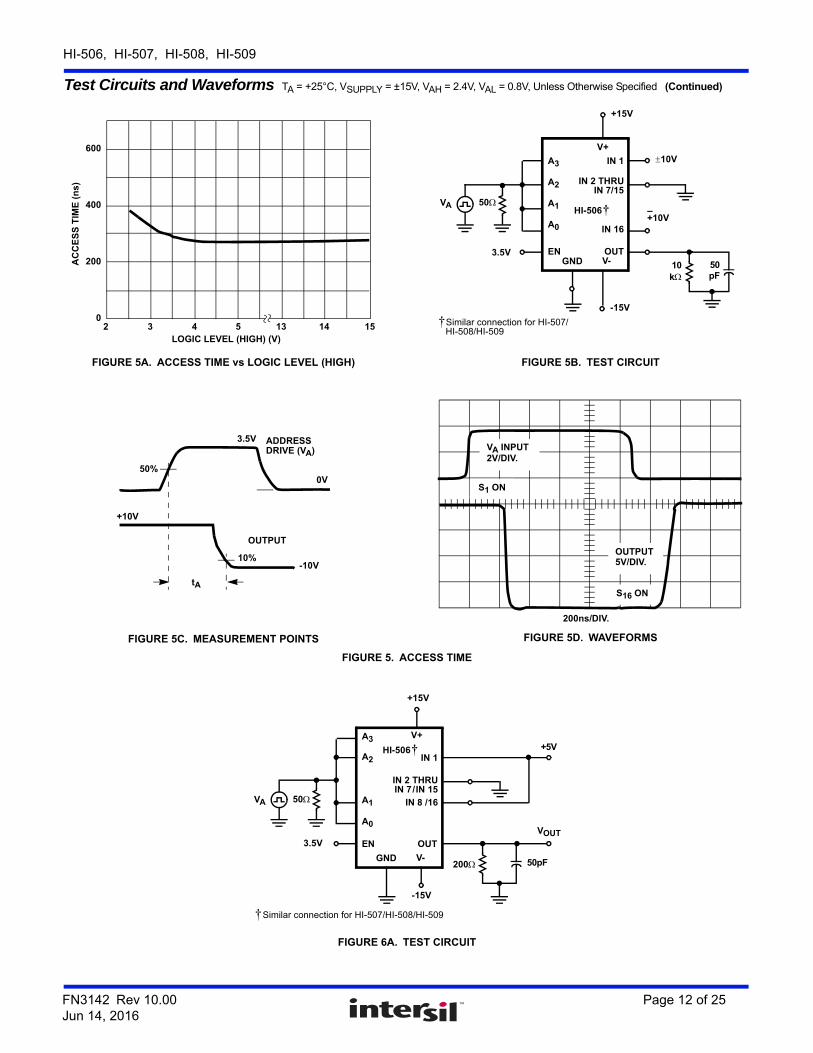
FIGURE 5A. ACCESS TIME vs LOGIC LEVEL (HIGH) FIGURE 5B. TEST CIRCUIT
FIGURE 5C. MEASUREMENT POINTS FIGURE 5D. WAVEFORMS
FIGURE 5. ACCESS TIME
FIGURE 6A. TEST CIRCUIT
Test Circuits and Waveforms TA = +25°C, VSUPPLY = ±15V, VAH = 2.4V, VAL = 0.8V, Unless Otherwise Specified (Continued)
600
400
200
02
AC
CE
SS
TIM
E (
ns
)
LOGIC LEVEL (HIGH) (V)3 4 5 151413
10V
+15V
V+
V-
IN 1
IN 2 THRU
IN 16
OUT
A0
EN
A1
10 50k pF
A3
A2
50VA
3.5VGND
-15V
+10V
IN 7/15
HI-506†
†Similar connection for HI-507/HI-508/HI-509
50%
3.5V
10%
+10V
0V
OUTPUT
-10V
tA
ADDRESSDRIVE (VA)
200ns/DIV.
S1 ON
S16 ON
VA INPUT2V/DIV.
OUTPUT5V/DIV.
+15V
V+
V-
IN 1
IN 2 THRU
IN 8 /16
OUT
A0
EN
A1
50pF200
VOUT
-15V
A3
A2
50VA
3.5V
GND
+5V
IN 7/IN 15
HI-506†
†Similar connection for HI-507/HI-508/HI-509
FN3142 Rev 10.00 Page 12 of 25Jun 14, 2016
HI-506, HI-507, HI-508, HI-509
FIGURE 6B. MEASUREMENT POINTS FIGURE 6C. WAVEFORMS
FIGURE 6. BREAK-BEFORE-MAKE DELAY
FIGURE 7A. TEST CIRCUIT
FIGURE 7B. MEASUREMENT POINTS FIGURE 7C. WAVEFORMS
FIGURE 7. ENABLE DELAYS
Test Circuits and Waveforms TA = +25°C, VSUPPLY = ±15V, VAH = 2.4V, VAL = 0.8V, Unless Otherwise Specified (Continued)
50% 50%
3.5V
0V
OUTPUT
ADDRESSDRIVE (VA)
tOPEN
S1 ON S16 ON
VA INPUT2V/DIV.
OUTPUT1V/DIV.
100ns/DIV.
+15V
V+
V-
IN 1
IN 2 THRU
IN 8 /16
OUT
A0
EN
A1
50pF200
VOUT
-15V
A3
A2
VAGND
+10V
IN 7/IN 15
HI-506†
†Similar connection for HI-507/HI-508/HI-509
50
3.5V
0V
OUTPUT
tOFF(EN)
ENABLE DRIVE (VA)
10%
50%50%
90%
tON(EN)
0V
DISABLED
OUTPUT2V/DIV.
ENABLEDRIVE2V/DIV.
ENABLED(S1 ON)
100ns/DIV
FN3142 Rev 10.00 Page 13 of 25Jun 14, 2016
HI-506, HI-507, HI-508, HI-509
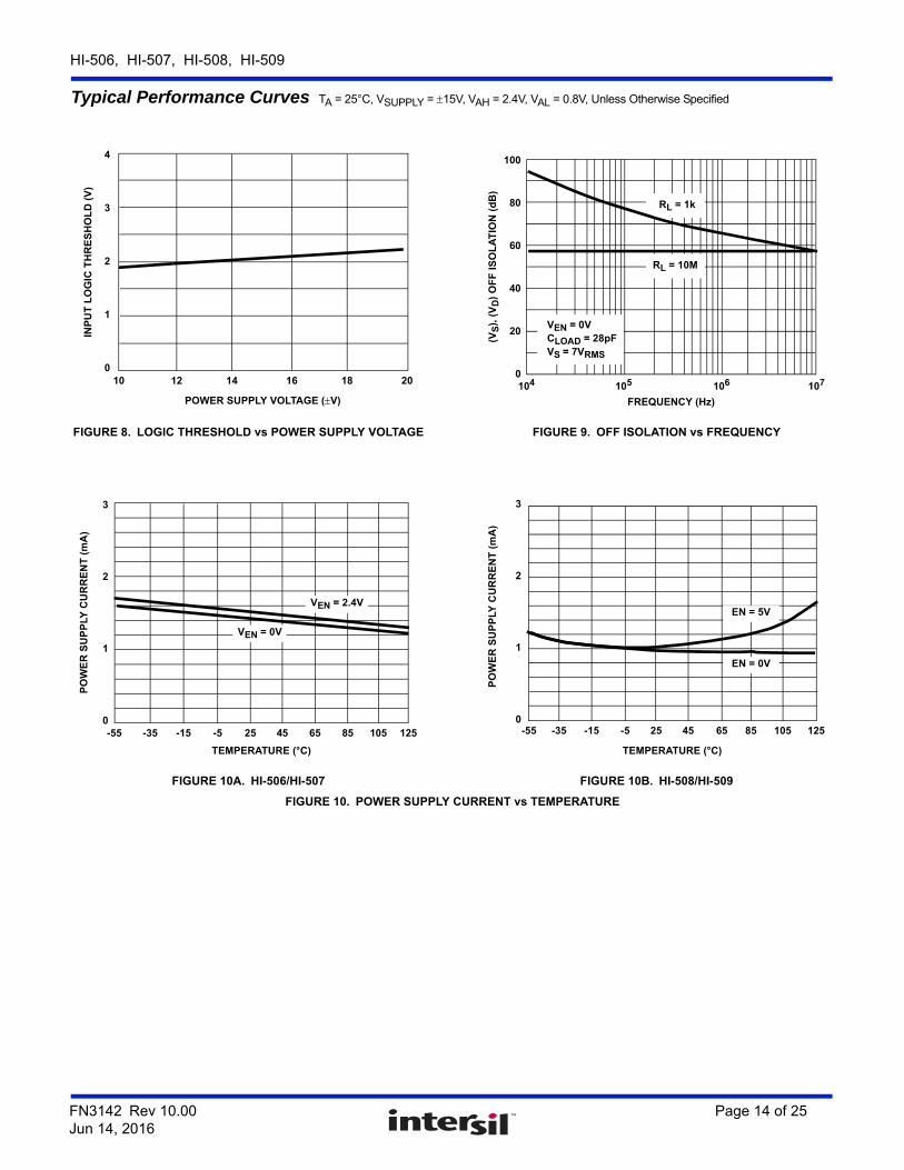
Typical Performance Curves TA = 25°C, VSUPPLY = 15V, VAH = 2.4V, VAL = 0.8V, Unless Otherwise Specified
FIGURE 8. LOGIC THRESHOLD vs POWER SUPPLY VOLTAGE FIGURE 9. OFF ISOLATION vs FREQUENCY
FIGURE 10A. HI-506/HI-507 FIGURE 10B. HI-508/HI-509
FIGURE 10. POWER SUPPLY CURRENT vs TEMPERATURE
10 12 14 16 18 20
POWER SUPPLY VOLTAGE (V)
INP
UT
LO
GIC
TH
RE
SH
OL
D (
V)
4
3
2
1
0
100
80
60
40
20
0104
(VS
), (
VD
) O
FF
ISO
LA
TIO
N (
dB
)
105 106 107
FREQUENCY (Hz)
VEN = 0VCLOAD = 28pFVS = 7VRMS
RL = 1k
RL = 10M
3
2
1
0
PO
WE
R S
UP
PLY
CU
RR
EN
T (
mA
)
-55
TEMPERATURE (°C)
-35 -15 -5 4525 65 85 105 125
VEN = 2.4V
VEN = 0V
3
2
1
0-55
PO
WE
R S
UP
PLY
CU
RR
EN
T (
mA
)
TEMPERATURE (°C)
-35 -15 -5 25 45 65 85 105 125
EN = 5V
EN = 0V
FN3142 Rev 10.00 Page 14 of 25Jun 14, 2016
HI-506, HI-507, HI-508, HI-509
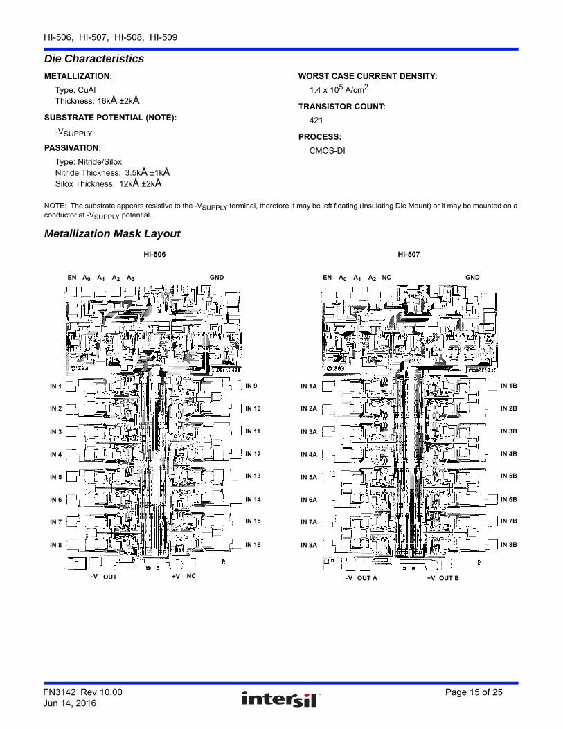
Die Characteristics
METALLIZATION:
Type: CuAlThickness: 16kÅ ±2kÅ
SUBSTRATE POTENTIAL (NOTE):
-VSUPPLY
PASSIVATION:
Type: Nitride/SiloxNitride Thickness: 3.5kÅ ±1kÅSilox Thickness: 12kÅ ±2kÅ
WORST CASE CURRENT DENSITY:
1.4 x 10⁵ A/cm2
TRANSISTOR COUNT:
421
PROCESS:
CMOS-DI
NOTE: The substrate appears resistive to the -VSUPPLY terminal, therefore it may be left floating (Insulating Die Mount) or it may be mounted on a conductor at -VSUPPLY potential.
Metallization Mask Layout
HI-506 HI-507
+V
IN 16
IN 15
IN 14
IN 13
IN 12
IN 11
IN 10
IN 9
GND
NC
A3
OUT
IN 8
IN 7
IN 6
IN 5
IN 3
IN 1
EN A0 A1 A2
-V
IN 4
IN 2
+V
IN 8B
IN 7B
IN 6B
IN 5B
IN 4B
IN 3B
IN 2B
IN 1B
GND
OUT B
NC
OUT A
IN 8A
IN 7A
IN 6A
IN 5A
IN 3A
IN 1A
EN A0 A1 A2
-V
IN 4A
IN 2A
FN3142 Rev 10.00 Page 15 of 25Jun 14, 2016
HI-506, HI-507, HI-508, HI-509
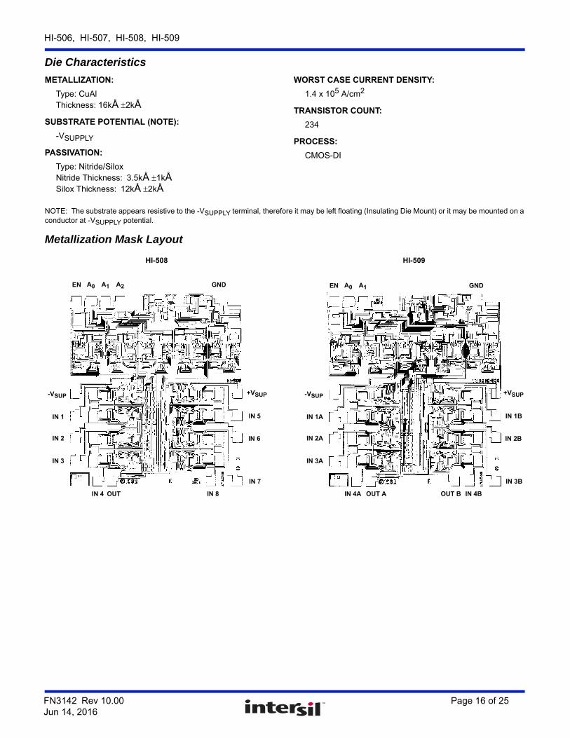
Die Characteristics
METALLIZATION:
Type: CuAlThickness: 16kÅ 2kÅ
SUBSTRATE POTENTIAL (NOTE):
-VSUPPLY
PASSIVATION:
Type: Nitride/SiloxNitride Thickness: 3.5kÅ 1kÅSilox Thickness: 12kÅ 2kÅ
WORST CASE CURRENT DENSITY:
1.4 x 10⁵ A/cm2
TRANSISTOR COUNT:
234
PROCESS:
CMOS-DI
NOTE: The substrate appears resistive to the -VSUPPLY terminal, therefore it may be left floating (Insulating Die Mount) or it may be mounted on a conductor at -VSUPPLY potential.
Metallization Mask Layout
HI-508 HI-509
+VSUP
GND
OUT IN 8
IN 7
IN 6
IN 5
IN 3
IN 1
EN A0 A1 A2
-VSUP
IN 4
IN 2
+VSUP
GND
OUT A IN 4B
IN 3B
IN 2B
IN 1B
IN 3A
IN 1A
EN A0 A1
-VSUP
IN 4A
IN 2A
OUT B
FN3142 Rev 10.00 Page 16 of 25Jun 14, 2016
HI-506, HI-507, HI-508, HI-509
About IntersilIntersil Corporation is a leading provider of innovative power management and precision analog solutions. The company's products address some of the largest markets within the industrial and infrastructure, mobile computing and high-end consumer markets.
For the most updated datasheet, application notes, related documentation and related parts, please see the respective product information page found at www.intersil.com.
You may report errors or suggestions for improving this datasheet by visiting www.intersil.com/ask.
Reliability reports are also available from our website at www.intersil.com/support
Revision HistoryThe revision history provided is for informational purposes only and is believed to be accurate, but not warranted. Please go to the web to make sure that you have the latest revision.
DATE REVISION CHANGE
May 24, 2016 FN3142.10 Updated ordering information table on page 2.
August 7, 2015 FN3142.9 Updated ordering information table on page 2.Added Revision History and About Intersil sections.Updated M28.3 to most recent revision with change as follows:Added land pattern
FN3142 Rev 10.00 Page 17 of 25Jun 14, 2016
HI-506, HI-507, HI-508, HI-509
FN3142 Rev 10.00 Page 18 of 25Jun 14, 2016
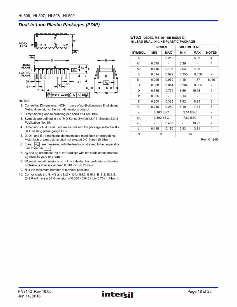
Dual-In-Line Plastic Packages (PDIP)
NOTES:
1. Controlling Dimensions: INCH. In case of conflict between English and Metric dimensions, the inch dimensions control.
2. Dimensioning and tolerancing per ANSI Y14.5M-1982.
3. Symbols are defined in the “MO Series Symbol List” in Section 2.2 of Publication No. 95.
4. Dimensions A, A1 and L are measured with the package seated in JE-DEC seating plane gauge GS-3.
5. D, D1, and E1 dimensions do not include mold flash or protrusions. Mold flash or protrusions shall not exceed 0.010 inch (0.25mm).
6. E and are measured with the leads constrained to be perpendic-ular to datum .
7. eB and eC are measured at the lead tips with the leads unconstrained. eC must be zero or greater.
8. B1 maximum dimensions do not include dambar protrusions. Dambar protrusions shall not exceed 0.010 inch (0.25mm).
9. N is the maximum number of terminal positions.
10. Corner leads (1, N, N/2 and N/2 + 1) for E8.3, E16.3, E18.3, E28.3, E42.6 will have a B1 dimension of 0.030 - 0.045 inch (0.76 - 1.14mm).
eA-C-
CL
E
eA
C
eB
eC
-B-
E1INDEX
1 2 3 N/2
N
AREA
SEATING
BASEPLANE
PLANE
-C-
D1
B1B
e
D
D1
AA2
L
A1
-A-
0.010 (0.25) C AM B S
E16.3 (JEDEC MS-001-BB ISSUE D)16 LEAD DUAL-IN-LINE PLASTIC PACKAGE
SYMBOL
INCHES MILLIMETERS
NOTESMIN MAX MIN MAX
A - 0.210 - 5.33 4
A1 0.015 - 0.39 - 4
A2 0.115 0.195 2.93 4.95 -
B 0.014 0.022 0.356 0.558 -
B1 0.045 0.070 1.15 1.77 8, 10
C 0.008 0.014 0.204 0.355 -
D 0.735 0.775 18.66 19.68 5
D1 0.005 - 0.13 - 5
E 0.300 0.325 7.62 8.25 6
E1 0.240 0.280 6.10 7.11 5
e 0.100 BSC 2.54 BSC -
eA 0.300 BSC 7.62 BSC 6
eB - 0.430 - 10.92 7
L 0.115 0.150 2.93 3.81 4
N 16 16 9
Rev. 0 12/93
HI-506, HI-507, HI-508, HI-509
FN3142 Rev 10.00 Page 19 of 25Jun 14, 2016
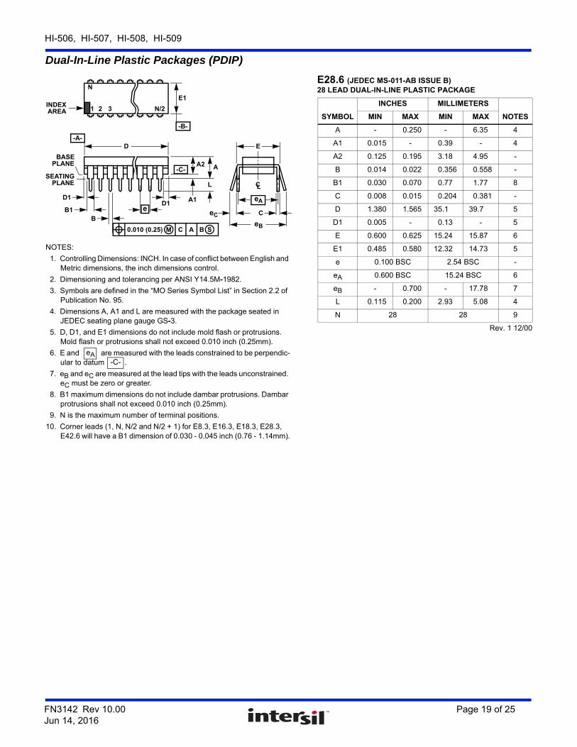
Dual-In-Line Plastic Packages (PDIP)
NOTES:
1. Controlling Dimensions: INCH. In case of conflict between English and Metric dimensions, the inch dimensions control.
2. Dimensioning and tolerancing per ANSI Y14.5M-1982.
3. Symbols are defined in the “MO Series Symbol List” in Section 2.2 of Publication No. 95.
4. Dimensions A, A1 and L are measured with the package seated in JEDEC seating plane gauge GS-3.
5. D, D1, and E1 dimensions do not include mold flash or protrusions. Mold flash or protrusions shall not exceed 0.010 inch (0.25mm).
6. E and are measured with the leads constrained to be perpendic-ular to datum .
7. eB and eC are measured at the lead tips with the leads unconstrained. eC must be zero or greater.
8. B1 maximum dimensions do not include dambar protrusions. Dambar protrusions shall not exceed 0.010 inch (0.25mm).
9. N is the maximum number of terminal positions.
10. Corner leads (1, N, N/2 and N/2 + 1) for E8.3, E16.3, E18.3, E28.3, E42.6 will have a B1 dimension of 0.030 - 0.045 inch (0.76 - 1.14mm).
eA-C-
CL
E
eA
C
eB
eC
-B-
E1INDEX
1 2 3 N/2
N
AREA
SEATING
BASEPLANE
PLANE
-C-
D1
B1B
e
D
D1
AA2
L
A1
-A-
0.010 (0.25) C AM B S
E28.6 (JEDEC MS-011-AB ISSUE B)28 LEAD DUAL-IN-LINE PLASTIC PACKAGE
SYMBOL
INCHES MILLIMETERS
NOTESMIN MAX MIN MAX
A - 0.250 - 6.35 4
A1 0.015 - 0.39 - 4
A2 0.125 0.195 3.18 4.95 -
B 0.014 0.022 0.356 0.558 -
B1 0.030 0.070 0.77 1.77 8
C 0.008 0.015 0.204 0.381 -
D 1.380 1.565 35.1 39.7 5
D1 0.005 - 0.13 - 5
E 0.600 0.625 15.24 15.87 6
E1 0.485 0.580 12.32 14.73 5
e 0.100 BSC 2.54 BSC -
eA 0.600 BSC 15.24 BSC 6
eB - 0.700 - 17.78 7
L 0.115 0.200 2.93 5.08 4
N 28 28 9
Rev. 1 12/00

HI-506, HI-507, HI-508, HI-509
FN3142 Rev 10.00 Page 20 of 25Jun 14, 2016
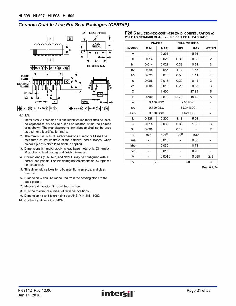
Ceramic Dual-In-Line Frit Seal Packages (CERDIP)
NOTES:
1. Index area: A notch or a pin one identification mark shall be locat-ed adjacent to pin one and shall be located within the shadedarea shown. The manufacturer’s identification shall not be usedas a pin one identification mark.
2. The maximum limits of lead dimensions b and c or M shall be measured at the centroid of the finished lead surfaces, whensolder dip or tin plate lead finish is applied.
3. Dimensions b1 and c1 apply to lead base metal only. Dimension M applies to lead plating and finish thickness.
4. Corner leads (1, N, N/2, and N/2+1) may be configured with a partial lead paddle. For this configuration dimension b3 replacesdimension b2.
5. This dimension allows for off-center lid, meniscus, and glass overrun.
6. Dimension Q shall be measured from the seating plane to the base plane.
7. Measure dimension S1 at all four corners.
8. N is the maximum number of terminal positions.
9. Dimensioning and tolerancing per ANSI Y14.5M - 1982.
10. Controlling dimension: INCH.
bbb C A - BS
c
Q
L
ASEATING
BASE
D
PLANE
PLANE
-D--A-
-C-
-B-
D
E
S1
b2
b
A
e
M
c1
b1
(c)
(b)
SECTION A-A
BASE
LEAD FINISH
METAL
eA/2
A
M
S S
ccc C A - BM DS S aaa C A - BM DS S
eA
F16.3 MIL-STD-1835 GDIP1-T16 (D-2, CONFIGURATION A)16 LEAD CERAMIC DUAL-IN-LINE FRIT SEAL PACKAGE
SYMBOL
INCHES MILLIMETERS
NOTESMIN MAX MIN MAX
A - 0.200 - 5.08 -
b 0.014 0.026 0.36 0.66 2
b1 0.014 0.023 0.36 0.58 3
b2 0.045 0.065 1.14 1.65 -
b3 0.023 0.045 0.58 1.14 4
c 0.008 0.018 0.20 0.46 2
c1 0.008 0.015 0.20 0.38 3
D - 0.840 - 21.34 5
E 0.220 0.310 5.59 7.87 5
e 0.100 BSC 2.54 BSC -
eA 0.300 BSC 7.62 BSC -
eA/2 0.150 BSC 3.81 BSC -
L 0.125 0.200 3.18 5.08 -
Q 0.015 0.060 0.38 1.52 6
S1 0.005 - 0.13 - 7
90o 105o 90o 105o -
aaa - 0.015 - 0.38 -
bbb - 0.030 - 0.76 -
ccc - 0.010 - 0.25 -
M - 0.0015 - 0.038 2, 3
N 16 16 8
Rev. 0 4/94
HI-506, HI-507, HI-508, HI-509
FN3142 Rev 10.00 Page 21 of 25Jun 14, 2016
Ceramic Dual-In-Line Frit Seal Packages (CERDIP)
NOTES:
1. Index area: A notch or a pin one identification mark shall be locat-ed adjacent to pin one and shall be located within the shadedarea shown. The manufacturer’s identification shall not be usedas a pin one identification mark.
2. The maximum limits of lead dimensions b and c or M shall be measured at the centroid of the finished lead surfaces, whensolder dip or tin plate lead finish is applied.
3. Dimensions b1 and c1 apply to lead base metal only. Dimension M applies to lead plating and finish thickness.
4. Corner leads (1, N, N/2, and N/2+1) may be configured with a partial lead paddle. For this configuration dimension b3 replacesdimension b2.
5. This dimension allows for off-center lid, meniscus, and glass overrun.
6. Dimension Q shall be measured from the seating plane to the base plane.
7. Measure dimension S1 at all four corners.
8. N is the maximum number of terminal positions.
9. Dimensioning and tolerancing per ANSI Y14.5M - 1982.
10. Controlling dimension: INCH.
bbb C A - BS
c
Q
L
ASEATING
BASE
D
PLANE
PLANE
-D--A-
-C-
-B-
D
E
S1
b2
b
A
e
M
c1
b1
(c)
(b)
SECTION A-A
BASE
LEAD FINISH
METAL
eA/2
A
M
S S
ccc C A - BM DS S aaa C A - BM DS S
eA
F28.6 MIL-STD-1835 GDIP1-T28 (D-10, CONFIGURATION A)28 LEAD CERAMIC DUAL-IN-LINE FRIT SEAL PACKAGE
SYMBOL
INCHES MILLIMETERS
NOTESMIN MAX MIN MAX
A - 0.232 - 5.92 -
b 0.014 0.026 0.36 0.66 2
b1 0.014 0.023 0.36 0.58 3
b2 0.045 0.065 1.14 1.65 -
b3 0.023 0.045 0.58 1.14 4
c 0.008 0.018 0.20 0.46 2
c1 0.008 0.015 0.20 0.38 3
D - 1.490 - 37.85 5
E 0.500 0.610 12.70 15.49 5
e 0.100 BSC 2.54 BSC -
eA 0.600 BSC 15.24 BSC -
eA/2 0.300 BSC 7.62 BSC -
L 0.125 0.200 3.18 5.08 -
Q 0.015 0.060 0.38 1.52 6
S1 0.005 - 0.13 - 7
90o 105o 90o 105o -
aaa - 0.015 - 0.38 -
bbb - 0.030 - 0.76 -
ccc - 0.010 - 0.25 -
M - 0.0015 - 0.038 2, 3
N 28 28 8
Rev. 0 4/94
HI-506, HI-507, HI-508, HI-509
FN3142 Rev 10.00 Page 22 of 25Jun 14, 2016
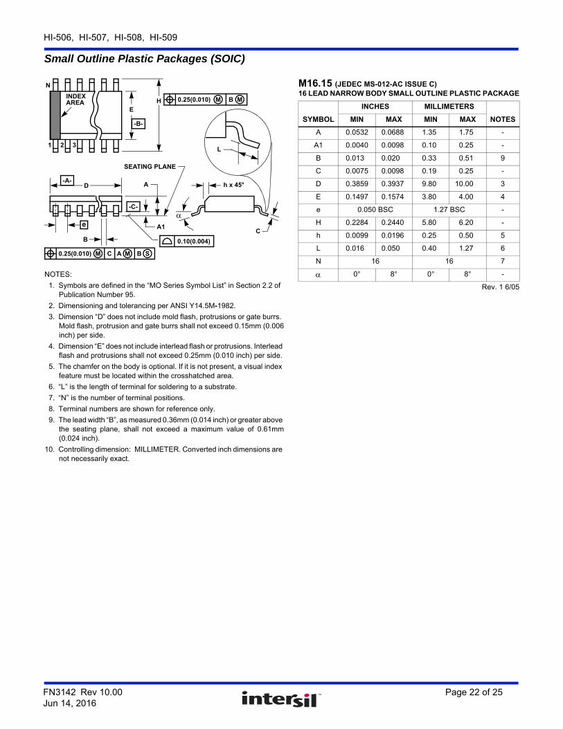
Small Outline Plastic Packages (SOIC)
NOTES:
1. Symbols are defined in the “MO Series Symbol List” in Section 2.2 of Publication Number 95.
2. Dimensioning and tolerancing per ANSI Y14.5M-1982.
3. Dimension “D” does not include mold flash, protrusions or gate burrs. Mold flash, protrusion and gate burrs shall not exceed 0.15mm (0.006inch) per side.
4. Dimension “E” does not include interlead flash or protrusions. Interlead flash and protrusions shall not exceed 0.25mm (0.010 inch) per side.
5. The chamfer on the body is optional. If it is not present, a visual index feature must be located within the crosshatched area.
6. “L” is the length of terminal for soldering to a substrate.
7. “N” is the number of terminal positions.
8. Terminal numbers are shown for reference only.
9. The lead width “B”, as measured 0.36mm (0.014 inch) or greater above the seating plane, shall not exceed a maximum value of 0.61mm(0.024 inch).
10. Controlling dimension: MILLIMETER. Converted inch dimensions are not necessarily exact.
INDEXAREA
E
D
N
1 2 3
-B-
0.25(0.010) C AM B S
e
-A-
L
B
M
-C-
A1
A
SEATING PLANE
0.10(0.004)
h x 45°
C
H 0.25(0.010) BM M
M16.15 (JEDEC MS-012-AC ISSUE C)16 LEAD NARROW BODY SMALL OUTLINE PLASTIC PACKAGE
SYMBOL
INCHES MILLIMETERS
NOTESMIN MAX MIN MAX
A 0.0532 0.0688 1.35 1.75 -
A1 0.0040 0.0098 0.10 0.25 -
B 0.013 0.020 0.33 0.51 9
C 0.0075 0.0098 0.19 0.25 -
D 0.3859 0.3937 9.80 10.00 3
E 0.1497 0.1574 3.80 4.00 4
e 0.050 BSC 1.27 BSC -
H 0.2284 0.2440 5.80 6.20 -
h 0.0099 0.0196 0.25 0.50 5
L 0.016 0.050 0.40 1.27 6
N 16 16 7
0° 8° 0° 8° -
Rev. 1 6/05
HI-506, HI-507, HI-508, HI-509
FN3142 Rev 10.00 Page 23 of 25Jun 14, 2016
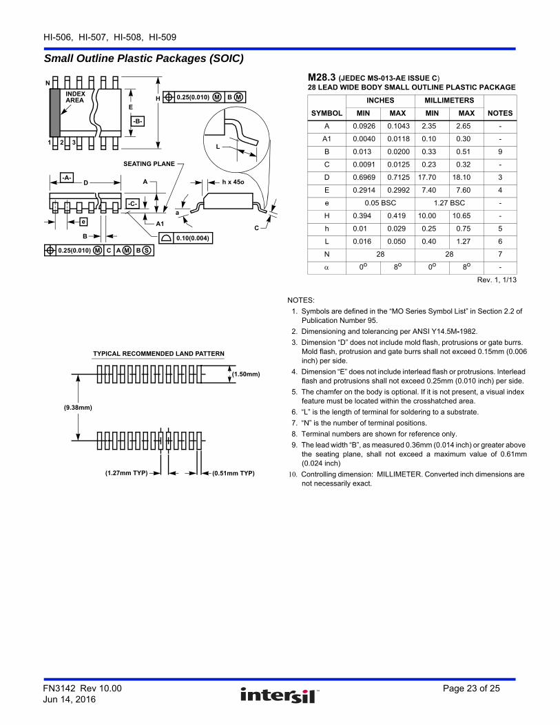
Small Outline Plastic Packages (SOIC)
a
INDEXAREA
E
D
N
1 2 3
-B-
0.25(0.010) C AM B S
e
-A-
L
B
M
-C-
A1
A
SEATING PLANE
0.10(0.004)
h x 45o
C
H 0.25(0.010) BM M
(1.50mm)
(9.38mm)
(1.27mm TYP) (0.51mm TYP)
TYPICAL RECOMMENDED LAND PATTERN
M28.3 (JEDEC MS-013-AE ISSUE C)28 LEAD WIDE BODY SMALL OUTLINE PLASTIC PACKAGE
SYMBOL
INCHES MILLIMETERS
NOTESMIN MAX MIN MAX
A 0.0926 0.1043 2.35 2.65 -
A1 0.0040 0.0118 0.10 0.30 -
B 0.013 0.0200 0.33 0.51 9
C 0.0091 0.0125 0.23 0.32 -
D 0.6969 0.7125 17.70 18.10 3
E 0.2914 0.2992 7.40 7.60 4
e 0.05 BSC 1.27 BSC -
H 0.394 0.419 10.00 10.65 -
h 0.01 0.029 0.25 0.75 5
L 0.016 0.050 0.40 1.27 6
N 28 28 7
0o 8o 0o 8o -
Rev. 1, 1/13
NOTES:
1. Symbols are defined in the “MO Series Symbol List” in Section 2.2 of Publication Number 95.
2. Dimensioning and tolerancing per ANSI Y14.5M-1982.
3. Dimension “D” does not include mold flash, protrusions or gate burrs. Mold flash, protrusion and gate burrs shall not exceed 0.15mm (0.006inch) per side.
4. Dimension “E” does not include interlead flash or protrusions. Interlead flash and protrusions shall not exceed 0.25mm (0.010 inch) per side.
5. The chamfer on the body is optional. If it is not present, a visual index feature must be located within the crosshatched area.
6. “L” is the length of terminal for soldering to a substrate.
7. “N” is the number of terminal positions.
8. Terminal numbers are shown for reference only.
9. The lead width “B”, as measured 0.36mm (0.014 inch) or greater above the seating plane, shall not exceed a maximum value of 0.61mm(0.024 inch)
10. Controlling dimension: MILLIMETER. Converted inch dimensions are not necessarily exact.
HI-506, HI-507, HI-508, HI-509
FN3142 Rev 10.00 Page 24 of 25Jun 14, 2016
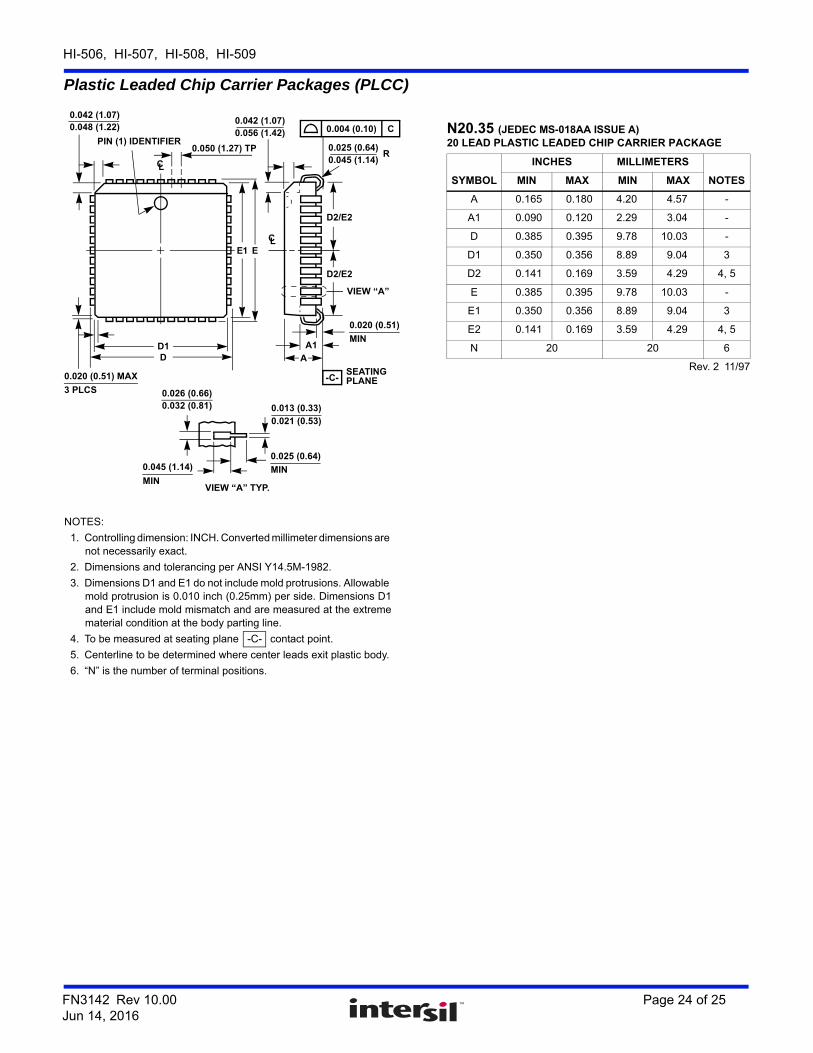
Plastic Leaded Chip Carrier Packages (PLCC)
A1
A
SEATINGPLANE
0.020 (0.51)
MIN
VIEW “A”
D2/E2
0.025 (0.64)0.045 (1.14)
R
0.042 (1.07)0.056 (1.42)
0.050 (1.27) TP
EE1
0.042 (1.07)0.048 (1.22)
PIN (1) IDENTIFIER
CL
D1D
0.020 (0.51) MAX
3 PLCS 0.026 (0.66)0.032 (0.81)
0.045 (1.14)
MIN
0.013 (0.33)
0.021 (0.53)
0.025 (0.64)
MIN
VIEW “A” TYP.
0.004 (0.10) C
-C-
D2/E2
CL
NOTES:
1. Controlling dimension: INCH. Converted millimeter dimensions are not necessarily exact.
2. Dimensions and tolerancing per ANSI Y14.5M-1982.
3. Dimensions D1 and E1 do not include mold protrusions. Allowable mold protrusion is 0.010 inch (0.25mm) per side. Dimensions D1and E1 include mold mismatch and are measured at the extremematerial condition at the body parting line.
4. To be measured at seating plane contact point.
5. Centerline to be determined where center leads exit plastic body.
6. “N” is the number of terminal positions.
-C-
N20.35 (JEDEC MS-018AA ISSUE A)20 LEAD PLASTIC LEADED CHIP CARRIER PACKAGE
SYMBOL
INCHES MILLIMETERS
NOTESMIN MAX MIN MAX
A 0.165 0.180 4.20 4.57 -
A1 0.090 0.120 2.29 3.04 -
D 0.385 0.395 9.78 10.03 -
D1 0.350 0.356 8.89 9.04 3
D2 0.141 0.169 3.59 4.29 4, 5
E 0.385 0.395 9.78 10.03 -
E1 0.350 0.356 8.89 9.04 3
E2 0.141 0.169 3.59 4.29 4, 5
N 20 20 6
Rev. 2 11/97
FN3142 Rev 10.00 Page 25 of 25Jun 14, 2016
HI-506, HI-507, HI-508, HI-509
Intersil products are manufactured, assembled and tested utilizing ISO9001 quality systems as notedin the quality certifications found at www.intersil.com/en/support/qualandreliability.html
Intersil products are sold by description only. Intersil may modify the circuit design and/or specifications of products at any time without notice, provided that such modification does not, in Intersil's sole judgment, affect the form, fit or function of the product. Accordingly, the reader is cautioned to verify that datasheets are current before placing orders. Information furnished by Intersil is believed to be accurate and reliable. However, no responsibility is assumed by Intersil or its subsidiaries for its use; nor for any infringements of patents or other rights of third parties which may result from its use. No license is granted by implication or otherwise under any patent or patent rights of Intersil or its subsidiaries.
For information regarding Intersil Corporation and its products, see www.intersil.com
For additional products, see www.intersil.com/en/products.html
© Copyright Intersil Americas LLC 2001-2016. All Rights Reserved.All trademarks and registered trademarks are the property of their respective owners.
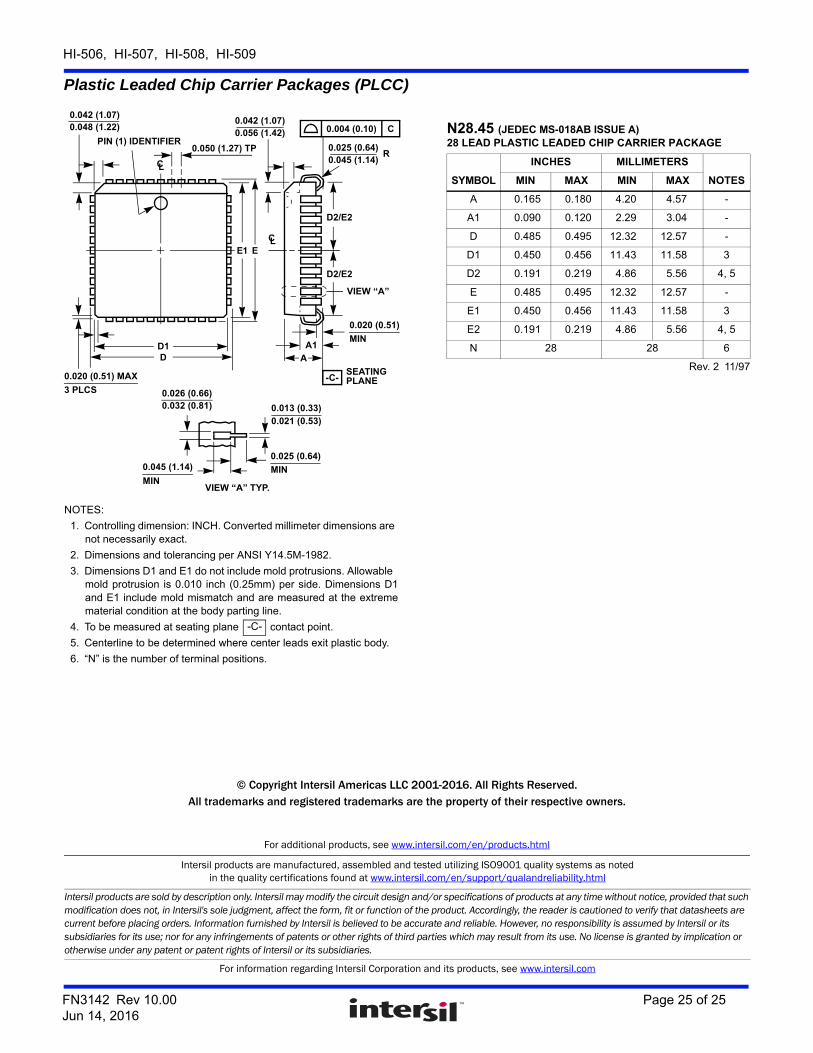
Plastic Leaded Chip Carrier Packages (PLCC)
NOTES:
1. Controlling dimension: INCH. Converted millimeter dimensions are not necessarily exact.
2. Dimensions and tolerancing per ANSI Y14.5M-1982.
3. Dimensions D1 and E1 do not include mold protrusions. Allowable mold protrusion is 0.010 inch (0.25mm) per side. Dimensions D1and E1 include mold mismatch and are measured at the extremematerial condition at the body parting line.
4. To be measured at seating plane contact point.
5. Centerline to be determined where center leads exit plastic body.
6. “N” is the number of terminal positions.
-C-
A1
A
SEATINGPLANE
0.020 (0.51)
MIN
VIEW “A”
D2/E2
0.025 (0.64)0.045 (1.14)
R
0.042 (1.07)0.056 (1.42)
0.050 (1.27) TP
EE1
0.042 (1.07)0.048 (1.22)
PIN (1) IDENTIFIER
CL
D1D
0.020 (0.51) MAX
3 PLCS 0.026 (0.66)0.032 (0.81)
0.045 (1.14)
MIN
0.013 (0.33)
0.021 (0.53)
0.025 (0.64)
MIN
VIEW “A” TYP.
0.004 (0.10) C
-C-
D2/E2
CL
N28.45 (JEDEC MS-018AB ISSUE A)28 LEAD PLASTIC LEADED CHIP CARRIER PACKAGE
SYMBOL
INCHES MILLIMETERS
NOTESMIN MAX MIN MAX
A 0.165 0.180 4.20 4.57 -
A1 0.090 0.120 2.29 3.04 -
D 0.485 0.495 12.32 12.57 -
D1 0.450 0.456 11.43 11.58 3
D2 0.191 0.219 4.86 5.56 4, 5
E 0.485 0.495 12.32 12.57 -
E1 0.450 0.456 11.43 11.58 3
E2 0.191 0.219 4.86 5.56 4, 5
N 28 28 6
Rev. 2 11/97
Related Documents