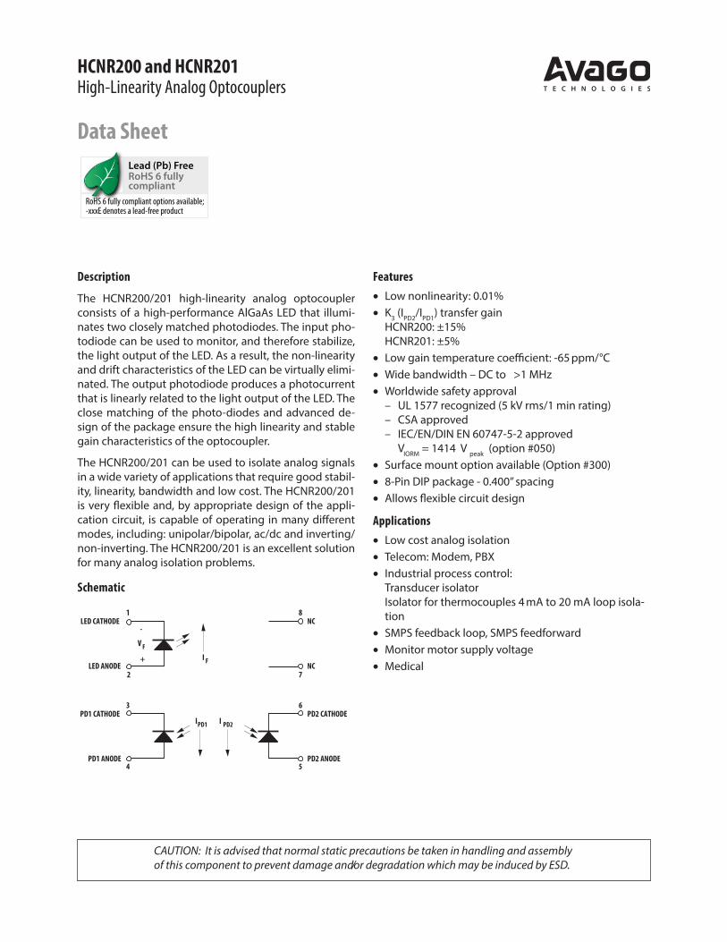
Features • Low nonlinearity: 0.01% • K 3 (I PD2 /I PD1 ) transfer gain HCNR200: ±15% HCNR201: ±5% • Low gain temperature coefficient: ‑65 ppm/°C • Wide bandwidth – DC to >1 MHz • Worldwide safety approval – UL 1577 recognized (5 kV rms/1 min rating) – CSA approved – IEC/EN/DIN EN 60747‑5‑2 approved V IORM = 1414 V peak (option #050) • Surface mount option available (Option #300) • 8‑Pin DIP package ‑ 0.400” spacing • Allows flexible circuit design Applications • Low cost analog isolation • Telecom: Modem, PBX • Industrial process control: Transducer isolator Isolator for thermocouples 4 mA to 20 mA loop isola‑ tion • SMPS feedback loop, SMPS feedforward • Monitor motor supply voltage • Medical Description The HCNR200/201 high‑linearity analog optocoupler consists of a high‑performance AlGaAs LED that illumi‑ nates two closely matched photodiodes. The input pho‑ todiode can be used to monitor, and therefore stabilize, the light output of the LED. As a result, the non‑linearity and drift characteristics of the LED can be virtually elimi‑ nated. The output photodiode produces a photocurrent that is linearly related to the light output of the LED. The close matching of the photo‑diodes and advanced de‑ sign of the package ensure the high linearity and stable gain characteristics of the optocoupler. The HCNR200/201 can be used to isolate analog signals in a wide variety of applications that require good stabil‑ ity, linearity, bandwidth and low cost. The HCNR200/201 is very flexible and, by appropriate design of the appli‑ cation circuit, is capable of operating in many different modes, including: unipolar/bipolar, ac/dc and inverting/ non‑inverting. The HCNR200/201 is an excellent solution for many analog isolation problems. Schematic HCNR200 and HCNR201 High-Linearity Analog Optocouplers Data Sheet CAUTION: It is advised that normal static precautions be taken in handling and assembly of this component to prevent damage and/or degradation which may be induced by ESD. Lead (Pb) Free RoHS 6 fully compliant RoHS 6 fully compliant options available; -xxxE denotes a lead-free product 3 4 1 2 V F - + I F I PD1 6 5 I PD2 8 7 NC NC PD2 CATHODE PD2 ANODE LED CATHODE LED ANODE PD1 CATHODE PD1 ANODE

Welcome message from author
This document is posted to help you gain knowledge. Please leave a comment to let me know what you think about it! Share it to your friends and learn new things together.
Transcript
Features• Low nonlinearity: 0.01%• K3 (IPD2/IPD1) transfer gain
HCNR200: ±15% HCNR201: ±5%
• Low gain temperature coefficient: ‑65 ppm/°C• Wide bandwidth – DC to >1 MHz• Worldwide safety approval
– UL 1577 recognized (5 kV rms/1 min rating) – CSA approved – IEC/EN/DIN EN 60747‑5‑2 approved VIORM = 1414 V peak (option #050)
• Surface mount option available (Option #300)• 8‑Pin DIP package ‑ 0.400” spacing• Allows flexible circuit design
Applications• Low cost analog isolation• Telecom: Modem, PBX• Industrial process control:
Transducer isolator Isolator for thermo couples 4 mA to 20 mA loop isola‑tion
• SMPS feedback loop, SMPS feedforward• Monitor motor supply voltage• Medical
Description
The HCNR200/201 high‑linearity analog optocoupler consists of a high‑performance AlGaAs LED that illumi‑nates two closely matched photodiodes. The input pho‑todiode can be used to monitor, and therefore stabilize, the light output of the LED. As a result, the non‑linearity and drift characteristics of the LED can be virtually elimi‑nated. The output photodiode produces a photocur rent that is linearly related to the light output of the LED. The close matching of the photo‑diodes and advanced de‑sign of the package ensure the high linearity and stable gain characteristics of the opto coupler.
The HCNR200/201 can be used to isolate analog signals in a wide variety of applications that require good stabil‑ity, linearity, bandwidth and low cost. The HCNR200/201 is very flexible and, by appro priate design of the appli‑cation circuit, is capable of operating in many different modes, includ ing: unipolar/bipolar, ac/dc and inverting/non‑inverting. The HCNR200/201 is an excellent solution for many analog isola tion problems.
Schematic
HCNR200 and HCNR201High-Linearity Analog Optocouplers
Data Sheet
CAUTION: It is advised that normal static precautions be taken in handling and assembly of this component to prevent damage and/or degradation which may be induced by ESD.
Lead (Pb) FreeRoHS 6 fullycompliant
RoHS 6 fully compliant options available;-xxxE denotes a lead-free product
3
4
1
2
V F
-
+ I F
IPD1
6
5
I PD2
8
7
NC
NC
PD2 CATHODE
PD2 ANODE
LED CATHODE
LED ANODE
PD1 CATHODE
PD1 ANODE

2
Ordering InformationHCNR200/HCNR201 is UL Recognized with 5000 Vrms for 1 minute per UL1577.
Option IEC/EN/DIN ENPart RoHS non RoHS Surface Gull Tape UL 5000 Vrms/ 60747-5-2 Number Compliant Compliant Package Mount Wing & Reel 1 Minute rating VIORM = 1414 Vpeak Quantity
‑000E no option 400 mil X 42 per tube
‑300E #300 Widebody X X X 42 per tube
HCNR200 ‑500E #500 DIP‑8 X X X X 750 per reel
HCNR201 ‑050E #050 X X 42 per tube
‑350E #350 X X X X 42 per tube
‑550E #550 X X X X X 750 per reel
To order, choose a part number from the part number column and combine with the desired option from the option column to form an order entry.
Example 1: HCNR200‑550E to order product of Gull Wing Surface Mount package in Tape and Reel packaging with IEC/EN/DIN EN 60747‑5‑2 VIORM = 1414 Vpeak Safety Approval and UL 5000 Vrms for 1 minute rating and RoHS compliant. Example 2: HCNR201 to order product of 8‑Pin Widebody DIP package in Tube packaging with UL 5000 Vrms for 1 minute rating and non RoHS compliant.
Option datasheets are available. Contact your Avago sales representative or authorized distributor for information.
Remarks: The notation ‘#XXX’ is used for existing products, while (new) products launched since July 15, 2001 and RoHS compliant will use ‘–XXXE.’
3
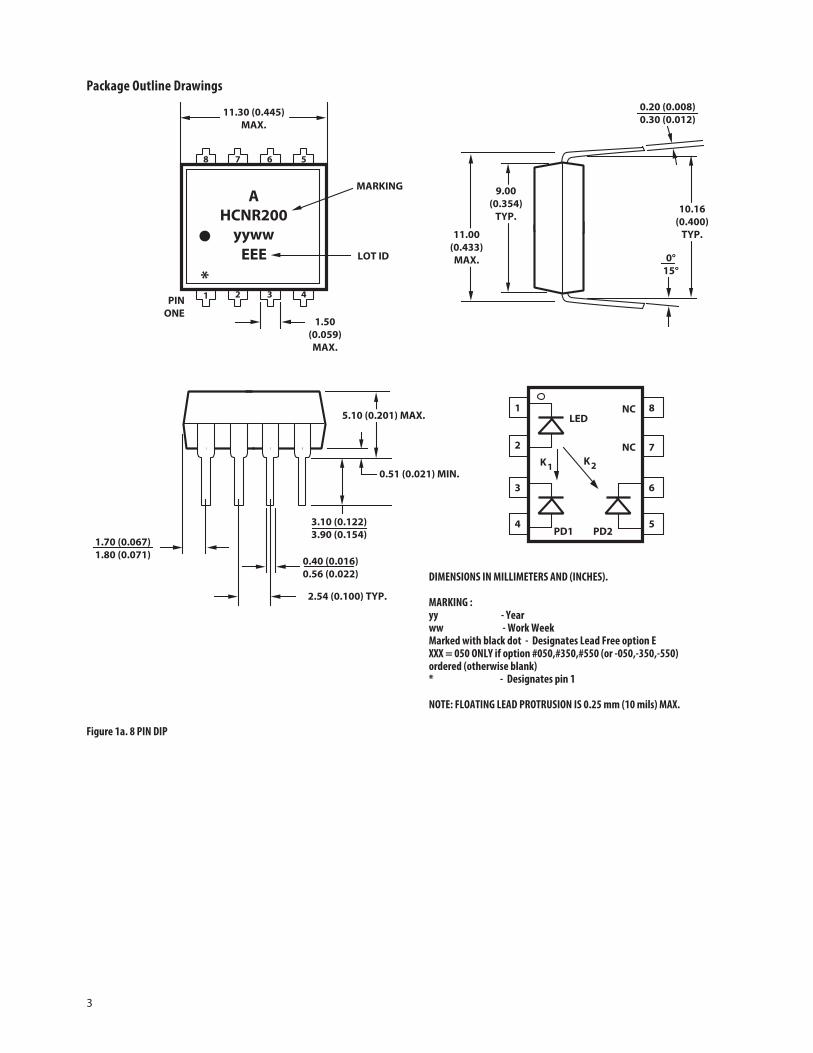
Package Outline Drawings
Figure 1a. 8 PIN DIP
0.40 (0.016)0.56 (0.022)
1
2
3
4
8
7
6
5
1.70 (0.067)1.80 (0.071)
2.54 (0.100) TYP.
0.51 (0.021) MIN.
5.10 (0.201) MAX.
3.10 (0.122)3.90 (0.154)
DIMENSIONS IN MILLIMETERS AND (INCHES).
MARKING : yy - Year ww - Work WeekMarked with black dot - Designates Lead Free option EXXX = 050 ONLY if option #050,#350,#550 (or -050,-350,-550) ordered (otherwise blank)* - Designates pin 1
NOTE: FLOATING LEAD PROTRUSION IS 0.25 mm (10 mils) MAX.
NC
PD1
K1
11.30 (0.445)MAX.
PINONE
1.50(0.059)MAX.
AHCNR200
yyww
MARKING
8 7 6 5
1 2 3 4
9.00(0.354)
TYP.
0.20 (0.008)0.30 (0.012)
0°15°
11.00(0.433)MAX.
10.16(0.400)
TYP.
K2
PD2
NC
LED
EEE
*LOT ID
4
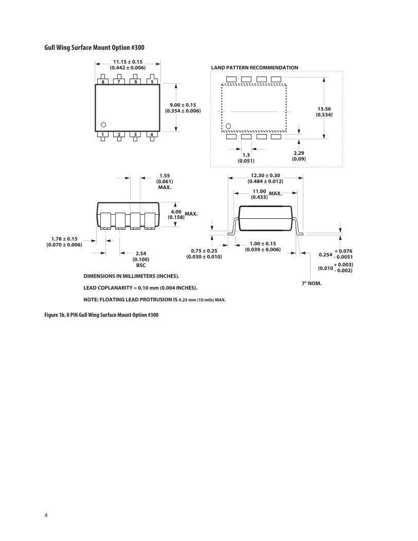
Gull Wing Surface Mount Option #300
1.00 ± 0.15(0.039 ± 0.006)
7° NOM.
12.30 ± 0.30(0.484 ± 0.012)
0.75 ± 0.25(0.030 ± 0.010)
11.00(0.433)
5678
4321
11.15 ± 0.15(0.442 ± 0.006)
9.00 ± 0.15(0.354 ± 0.006)
1.3(0.051)
13.56(0.534)
2.29(0.09)
LAND PATTERN RECOMMENDATION
1.78 ± 0.15(0.070 ± 0.006)
4.00(0.158)
MAX.
1.55(0.061)MAX.
2.54(0.100)
BSC
DIMENSIONS IN MILLIMETERS (INCHES).
LEAD COPLANARITY = 0.10 mm (0.004 INCHES).
NOTE: FLOATING LEAD PROTRUSION IS 0.25 mm (10 mils) MAX.
0.254+ 0.076- 0.0051
(0.010+ 0.003)- 0.002)
MAX.
Figure 1b. 8 PIN Gull Wing Surface Mount Option #300
5
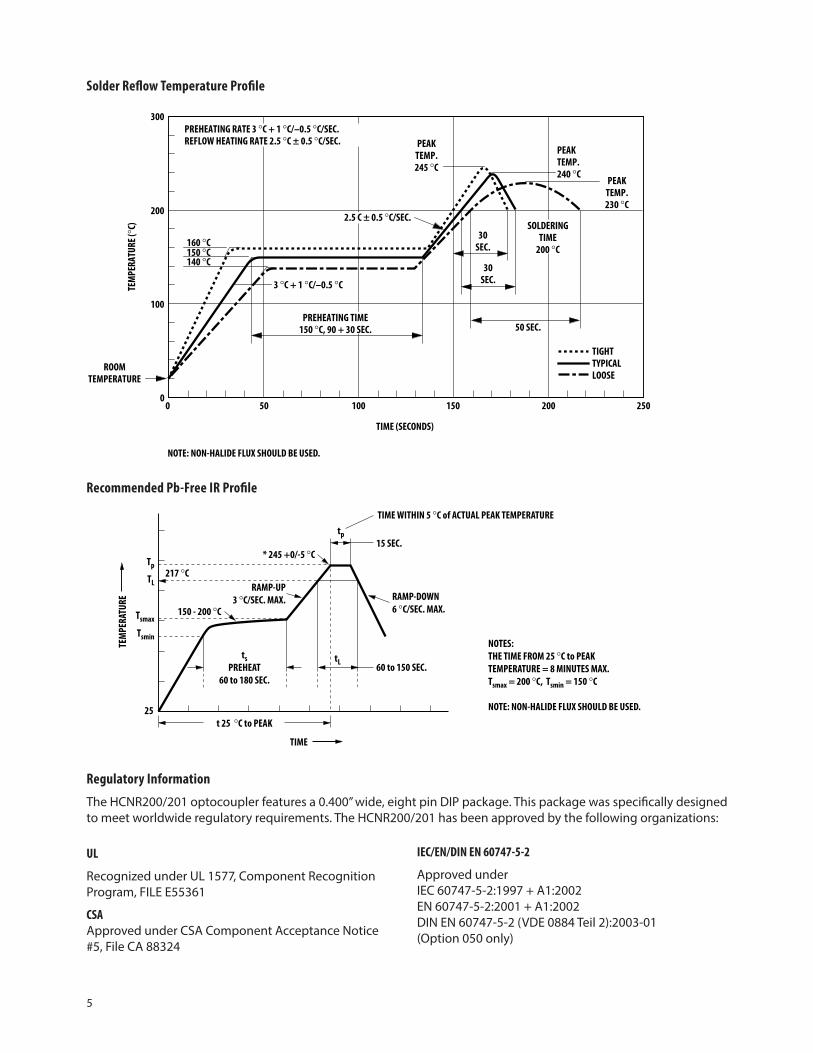
Solder Reflow Temperature Profile
Regulatory Information
The HCNR200/201 optocoupler features a 0.400” wide, eight pin DIP package. This package was specifically designed to meet worldwide regulatory require ments. The HCNR200/201 has been approved by the following organizations:
Recommended Pb-Free IR Profile
0
TIME (SECONDS)
TEM
PERA
TURE
(°C)
200
100
50 150100 200 250
300
0
30SEC.
50 SEC.
30SEC.
160 °C
140 °C150 °C
PEAKTEMP.245 °C
PEAKTEMP.240 °C
PEAKTEMP.230 °C
SOLDERINGTIME
200 °C
PREHEATING TIME150 °C, 90 + 30 SEC.
2.5 C ± 0.5 °C/SEC.
3 °C + 1 °C/–0.5 °C
TIGHTTYPICALLOOSE
ROOMTEMPERATURE
PREHEATING RATE 3 °C + 1 °C/–0.5 °C/SEC.REFLOW HEATING RATE 2.5 °C ± 0.5 °C/SEC.
NOTE: NON-HALIDE FLUX SHOULD BE USED.
217 °C
RAMP-DOWN6 °C/SEC. MAX.
RAMP-UP3 °C/SEC. MAX.
150 - 200 °C
* 245 +0/-5 °C
t 25 °C to PEAK
60 to 150 SEC.
15 SEC.
TIME WITHIN 5 °C of ACTUAL PEAK TEMPERATUREtp
tsPREHEAT
60 to 180 SEC.
tL
TL
Tsmax
Tsmin
25
Tp
TIME
TEM
PERA
TURE
NOTES:THE TIME FROM 25 °C to PEAKTEMPERATURE = 8 MINUTES MAX.Tsmax = 200 °C, Tsmin = 150 °C
NOTE: NON-HALIDE FLUX SHOULD BE USED.
UL
Recognized under UL 1577, Component Recognition Program, FILE E55361
CSA Approved under CSA Component Acceptance Notice #5, File CA 88324
IEC/EN/DIN EN 60747-5-2
Approved under IEC 60747‑5‑2:1997 + A1:2002 EN 60747‑5‑2:2001 + A1:2002 DIN EN 60747‑5‑2 (VDE 0884 Teil 2):2003‑01 (Option 050 only)

6
Insulation and Safety Related Specifications Parameter Symbol Value Units Conditions
Min. External Clearance L(IO1) 9.6 mm Measured from input terminals to output (External Air Gap) terminals, shortest distance through air
Min. External Creepage L(IO2) 10.0 mm Measured from input terminals to output (External Tracking Path) terminals, shortest distance path along body
Min. Internal Clearance 1.0 mm Through insulation distance conductor to (Internal Plastic Gap) conductor, usually the direct distance between the photoemitter and photodetector inside the optocoupler cavity
Min. Internal Creepage 4.0 mm The shortest distance around the border (Internal Tracking Path) between two different insulating materials measured between the emitter and detector
Comparative Tracking Index CTI 200 V DIN IEC 112/VDE 0303 PART 1
Isolation Group IIIa Material group (DIN VDE 0110)
Option 300 – surface mount classification is Class A in accordance with CECC 00802.
IEC/EN/DIN EN 60747-5-2 Insulation Characteristics (Option #050 Only)
Description Symbol Characteristic Unit
Installation classification per DIN VDE 0110/1.89, Table 1 For rated mains voltage ≤600 V rms I‑IV For rated mains voltage ≤1000 V rms I‑III
Climatic Classification (DIN IEC 68 part 1) 55/100/21
Pollution Degree (DIN VDE 0110 Part 1/1.89) 2
Maximum Working Insulation Voltage VIORM 1414 V peak
Input to Output Test Voltage, Method b* VPR 2651 V peak VPR = 1.875 x VIORM, 100% Production Test with tm = 1 sec, Partial Discharge < 5 pC
Input to Output Test Voltage, Method a* VPR 2121 V peak VPR = 1.5 x VIORM, Type and sample test, tm = 60 sec, Partial Discharge < 5 pC
Highest Allowable Overvoltage* VIOTM 8000 V peak (Transient Overvoltage, tini = 10 sec)
Safety‑Limiting Values (Maximum values allowed in the event of a failure, also see Figure 11) Case Temperature TS 150 °C Current (Input Current IF, PS = 0) IS 400 mA Output Power PS,OUTPUT 700 mW
Insulation Resistance at TS, VIO = 500 V RS >109 Ω
*Refer to the front of the Optocoupler section of the current catalog for a more detailed description of IEC/EN/DIN EN 60747‑5‑2 and other prod‑uct safety regulations.
Note: Optocouplers providing safe electrical separation per IEC/EN/DIN EN 60747‑5‑2 do so only within the safety‑limiting values to which they are qualified. Protective cut‑out switches must be used to ensure that the safety limits are not exceeded.

7
Absolute Maximum RatingsStorage Temperature ..............................................................................................‑55°C to +125°COperating Temperature (TA) ................................................................................. ‑55°C to +100°CJunction Temperature (TJ) ......................................................................................................... 125°CReflow Temperature Profile ..............................................See Package Outline Drawings SectionLead Solder Temperature ............................................................................................260°C for 10s (up to seating plane)Average Input Current ‑ IF ........................................................................................................ 25 mAPeak Input Current ‑ IF ............................................................................................................... 40 mA (50 ns maximum pulse width)Reverse Input Voltage ‑ VR ............................................................................................................2.5 V (IR = 100 µA, Pin 1‑2)Input Power Dissipation .................................................................................... 60 mW @ TA = 85°C (Derate at 2.2 mW/°C for operating temperatures above 85°C)Reverse Output Photodiode Voltage ........................................................................................30 V (Pin 6‑5)Reverse Input Photodiode Voltage ............................................................................................30 V (Pin 3‑4)
Recommended Operating ConditionsStorage Temperature .................................................................................................‑40°C to +85°COperating Temperature ............................................................................................ ‑40°C to +85°CAverage Input Current ‑ IF .................................................................................................. 1 ‑ 20 mAPeak Input Current ‑ IF ............................................................................................................... 35 mA (50% duty cycle, 1 ms pulse width)Reverse Output Photodiode Voltage ..................................................................................0 ‑ 15 V (Pin 6‑5)Reverse Input Photodiode Voltage ......................................................................................0 ‑ 15 V (Pin 3‑4)
8
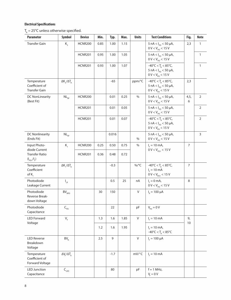
Electrical Specifications
TA = 25°C unless otherwise specified.
Parameter Symbol Device Min. Typ. Max. Units Test Conditions Fig. Note
Transfer Gain K3 HCNR200 0.85 1.00 1.15 5 nA < IPD < 50 µA, 2,3 1 0 V < VPD < 15 V
HCNR201 0.95 1.00 1.05 5 nA < IPD < 50 µA, 1 0 V < VPD < 15 V
HCNR201 0.93 1.00 1.07 ‑40°C < TA < 85°C, 1 5 nA < IPD < 50 µA, 0 V < VPD < 15 V
Temperature ∆K3/∆TA ‑65 ppm/°C ‑40°C < TA < 85°C, 2,3 Coefficient of 5 nA < IPD < 50 µA, Transfer Gain 0 V < VPD < 15 V
DC NonLinearity NLBF HCNR200 0.01 0.25 % 5 nA < IPD < 50 µA, 4,5, 2 (Best Fit) 0 V < VPD < 15 V 6
HCNR201 0.01 0.05 5 nA < IPD < 50 µA, 2 0 V < VPD < 15 V
HCNR201 0.01 0.07 ‑40°C < TA < 85°C, 2 5 nA < IPD < 50 µA, 0 V < VPD < 15 V
DC Nonlinearity NLEF 0.016 5 nA < IPD < 50 µA, 3 (Ends Fit) % 0 V < VPD < 15 V
Input Photo‑ K1 HCNR200 0.25 0.50 0.75 % IF = 10 mA, 7 diode Current 0 V < VPD1 < 15 V Transfer Ratio HCNR201 0.36 0.48 0.72 (IPD1/IF)
Temperature ∆K1/∆TA ‑0.3 %/°C ‑40°C < TA < 85°C, 7 Coefficient IF = 10 mA of K1 0 V < VPD1 < 15 V
Photodiode ILK 0.5 25 nA IF = 0 mA, 8 Leakage Current 0 V < VPD < 15 V
Photodiode BVRPD 30 150 V IR = 100 µA Reverse Break‑ down Voltage
Photodiode CPD 22 pF VPD = 0 V Capacitance
LED Forward VF 1.3 1.6 1.85 V IF = 10 mA 9, Voltage 10 1.2 1.6 1.95 IF = 10 mA, ‑40°C < TA < 85°C
LED Reverse BVR 2.5 9 V IF = 100 µA Breakdown Voltage
Temperature ∆VF/∆TA ‑1.7 mV/°C IF = 10 mA Coefficient of Forward Voltage
LED Junction CLED 80 pF f = 1 MHz, Capacitance VF = 0 V
9
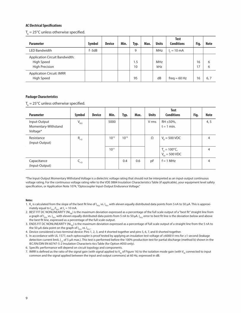
AC Electrical Specifications
TA = 25°C unless otherwise specified.
Test Parameter Symbol Device Min. Typ. Max. Units Conditions Fig. Note
LED Bandwidth f ‑3dB 9 MHz IF = 10 mA
Application Circuit Bandwidth: High Speed 1.5 MHz 16 6 High Precision 10 kHz 17 6
Application Circuit: IMRR High Speed 95 dB freq = 60 Hz 16 6, 7
Notes:1. K3 is calculated from the slope of the best fit line of IPD2 vs. IPD1 with eleven equally distributed data points from 5 nA to 50 µA. This is approxi‑
mately equal to IPD2/IPD1 at IF = 10 mA.2. BEST FIT DC NONLINEARITY (NLBF) is the maximum deviation expressed as a percentage of the full scale output of a “best fit” straight line from
a graph of IPD2 vs. IPD1 with eleven equally distrib uted data points from 5 nA to 50 µA. IPD2 error to best fit line is the deviation below and above the best fit line, expressed as a percentage of the full scale output.
3. ENDS FIT DC NONLINEARITY (NLEF) is the maximum deviation expressed as a percentage of full scale output of a straight line from the 5 nA to the 50 µA data point on the graph of IPD2 vs. IPD1.
4. Device considered a two‑terminal device: Pins 1, 2, 3, and 4 shorted together and pins 5, 6, 7, and 8 shorted together.5. In accordance with UL 1577, each optocoupler is proof tested by applying an insulation test voltage of ≥6000 V rms for ≥1 second (leakage
detection current limit, II‑O of 5 µA max.). This test is performed before the 100% production test for partial discharge (method b) shown in the IEC/EN/DIN EN 60747‑5‑2 Insulation Characteris‑tics Table (for Option #050 only).
6. Specific performance will depend on circuit topology and components.7. IMRR is defined as the ratio of the signal gain (with signal applied to VIN of Figure 16) to the isolation mode gain (with VIN connected to input
common and the signal applied between the input and output commons) at 60 Hz, expressed in dB.
Package Characteristics
TA = 25°C unless otherwise specified.
Test Parameter Symbol Device Min. Typ. Max. Units Conditions Fig. Note
Input‑Output VISO 5000 V rms RH ≤50%, 4, 5 Momentary‑Withstand t = 1 min. Voltage*
Resistance RI‑O 1012 1013 Ω VO = 500 VDC 4 (Input‑Output)
1011 TA = 100°C, 4 VIO = 500 VDC
Capacitance CI‑O 0.4 0.6 pF f = 1 MHz 4 (Input‑Output)
*The Input‑Output Momentary Withstand Voltage is a dielectric voltage rating that should not be interpreted as an input‑output continuous voltage rating. For the continuous voltage rating refer to the VDE 0884 Insulation Characteristics Table (if applicable), your equipment level safety specification, or Application Note 1074, “Optocoupler Input‑Output Endurance Voltage.”
10
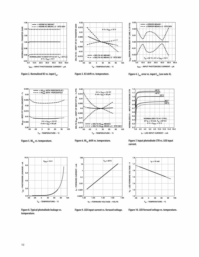
Figure 5. NLBF vs. temperature.
Figure 2. Normalized K3 vs. input IPD. Figure 3. K3 drift vs. temperature. Figure 4. IPD2 error vs. input IPD (see note 4).
Figure 6. NLBF drift vs. temperature. Figure 7. Input photodiode CTR vs. LED input current.
Figure 8. Typical photodiode leakage vs. temperature.
Figure 9. LED input current vs. forward voltage. Figure 10. LED forward voltage vs. temperature.
I LK
– P
HO
TO
DIO
DE
LE
AK
AG
E –
nA
10.0
4.0
0.0
TA – TEMPERATURE – °C
6.0
2.0
CNR200 fig 8
8.0
-25-55 5 35 65 95 125
VPD = 15 V
DE
LT
A K
3 –
DR
IFT
OF
K3
TR
AN
SF
ER
GA
IN
0.02
-0.005
-0.02
TA – TEMPERATURE – °C
0.01
0.005
-0.01
-0.015
HCNR200 fig 3
= DELTA K3 MEAN= DELTA K3 MEAN ± 2 • STD DEV
0.0
0.015
-25-55 5 35 65 95 125
0 V < VPD < 15 V
DE
LT
A N
LB
F –
DR
IFT
OF
BE
ST
-FIT
NL
– %
PT
S 0.02
-0.005
-0.02
TA – TEMPERATURE – °C
0.01
0.005
-0.01
-0.015
HCNR200 fig 6
= DELTA NLBF MEAN= DELTA NLBF MEAN ± 2 • STD DEV
0.0
0.015
-25-55 5 35 65 95 125
0 V < VPD < 15 V5 nA < IPD < 50 µA
NO
RM
AL
IZE
D K
1 –
INP
UT
PH
OT
OD
IOD
E C
TR
0.0
0.5
0.2
IF – LED INPUT CURRENT – mA
2.0 6.0 12.0
0.6
0.4
0.3
4.0 8.0 10.0
HCNR200 fig 7
0.7
0.8
0.9
1.0
1.1
1.2
14.0 16.0
-55°C
25°C-40°C
85°C100°C
NORMALIZED TO K1 CTRAT IF = 10 mA, TA = 25°C
0 V < VPD1 < 15 V
VF –
LE
D F
OR
WA
RD
VO
LT
AG
E –
V
1.5
1.2
TA – TEMPERATURE – °C
1.8
1.7
1.4
1.3
HCNR200 fig 10
1.6
-25-55 5 35 65 95 125
IF = 10 mA
NO
RM
AL
IZE
D K
3 –
TR
AN
SF
ER
GA
IN
0.0
1.06
1.00
0.94
IPD1 – INPUT PHOTODIODE CURRENT – µA
10.0 30.0 60.0
1.04
1.02
0.98
0.96
20.0 40.0 50.0
HCNR200 fig 2
= NORM K3 MEAN= NORM K3 MEAN ± 2 • STD DEV
NORMALIZED TO BEST-FIT K3 AT TA = 25°C,0 V < VPD < 15 V
0.0
0.03
0.00
-0.03
IPD1 – INPUT PHOTODIODE CURRENT – µA
10.0 30.0 60.0
0.02
0.01
-0.01
-0.02
20.0 40.0 50.0
HCNR200 fig 4
= ERROR MEAN= ERROR MEAN ± 2 • STD DEV
I PD
2 E
RR
OR
FR
OM
BE
ST
-FIT
LIN
E (
% O
F F
S)
TA = 25 °C, 0 V < VPD < 15 V
NL
BF –
BE
ST
-FIT
NO
N-L
INE
AR
ITY
– %
0.015
0.00
TA – TEMPERATURE – °C
0.03
0.025
0.01
0.005
HCNR200 fig 5
= NLBF 50TH PERCENTILE= NLBF 90TH PERCENTILE
0.02
0.035
-25-55 5 35 65 95 125
0 V < VPD < 15 V5 nA < IPD < 50 µA
1.20
100
0.1
0.0001
VF – FORWARD VOLTAGE – VOLTS
1.30 1.50
10
1
0.01
0.001
1.40 1.60
CNR200 fig 9
I F –
FO
RW
AR
D C
UR
RE
NT
– m
A
TA = 25°C
11
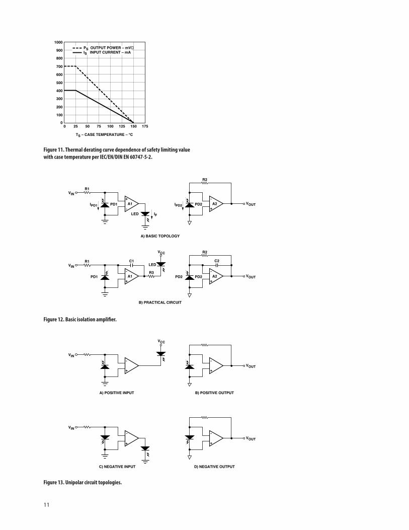
Figure 12. Basic isolation amplifier.
Figure 11. Thermal derating curve dependence of safety limiting value with case temperature per IEC/EN/DIN EN 60747-5-2.
Figure 13. Unipolar circuit topologies.
0
800
300
0
TS – CASE TEMPERATURE – °C
25 75 150
600
500
200
100
50 100 125
CNR200 fig 11
PS OUTPUT POWER – mVIS INPUT CURRENT – mA
400
700
900
1000
175
-
+
VIN-
+
VOUT
VIN-
+
-
+VOUT
A) POSITIVE INPUT
CNR200 fig 13
VCC
B) POSITIVE OUTPUT
C) NEGATIVE INPUT D) NEGATIVE OUTPUT
IFLED
IPD1 PD1
R1VIN
A1+
-IPD2 PD2
R2
A2-
+VOUT
PD1
R1VIN
A1-
+PD2 PD2
R2
A2-
+VOUT
A) BASIC TOPOLOGY
B) PRACTICAL CIRCUIT
CNR200 fig 12
C1
R3
VCC
LEDC2
12
Figure 15. Loop-powered 4-20 mA current loop circuits.
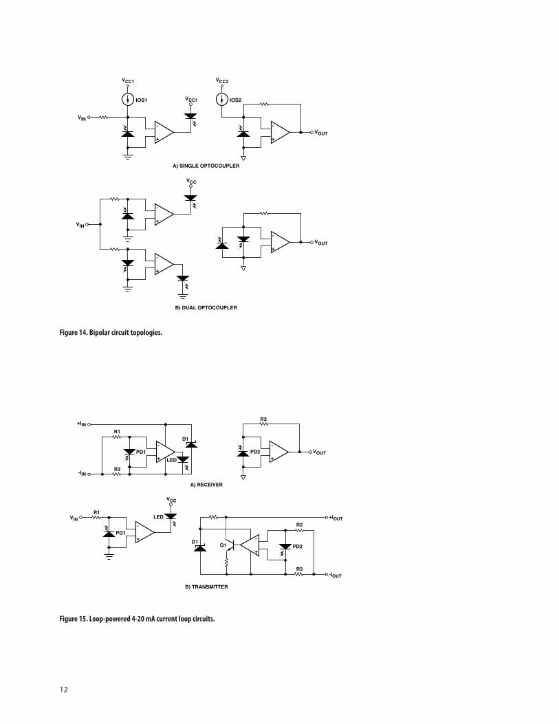
Figure 14. Bipolar circuit topologies.
-
+VOUT
+IIN
-
+
-
+
+IOUT
A) RECEIVER
CNR200 fig 15
B) TRANSMITTER
PD2
VIN-
+
VCC
-IIN
R1
R3
PD1
LED
D1
R2
R1
PD1
LED
-IOUT
R2
R3
PD2 D1
Q1
-
+
-
+
VOUT
VIN-
+
-
+VOUT
A) SINGLE OPTOCOUPLER
CNR200 fig 14
VCC1
B) DUAL OPTOCOUPLER
VCC1
IOS1
VCC2
IOS2
VIN
-
+
VCC
13
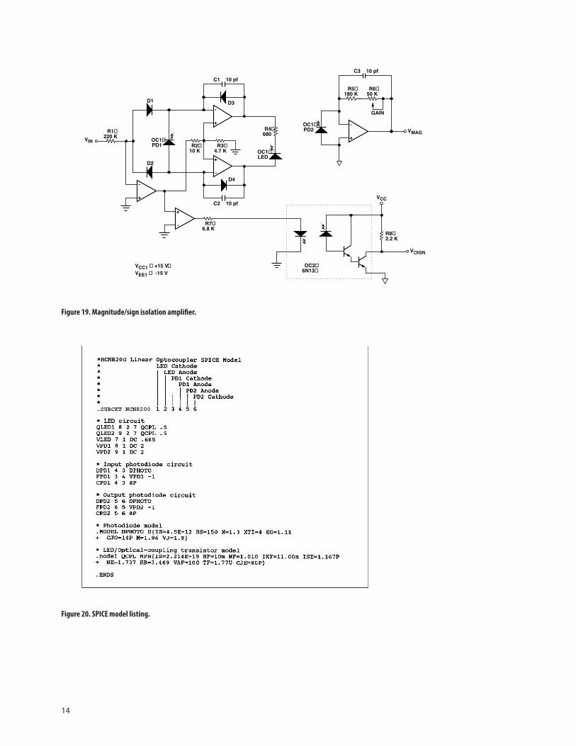
Figure 18. Bipolar isolation amplifier.
Figure 16. High-speed low-cost analog isolator.
Figure 17. Precision analog isolation amplifier.
-
+VMAG
-
+
VIN
OC1PD1
+
-
OC2PD1
R150 K
D2
C2 10 pf
C1 10 pf
D1R4680
R5680
OC1LED
OC2LED
R3180 K
R2180 K
BALANCE
C3 10 pf
OC1PD2
R6180 K
R50 K
GAIN
OC2PD2
VCC1 +15 VVEE1 -15 V
CNR200 fig 16
VIN
VCC1 +5 V
R168 K
PD1
LEDR310 K
Q12N3906
R410
Q22N3904
VCC2 +5 V
R268 K
PD2
R510 K
Q32N3906
R610
Q42N3904
R7470
VOUT
CNR200 fig 17
-
+PD1
23 A1
7
4
R1 200 KINPUT
BNC 1%
C3 0.1µ
VCC1 +15 V
C1 47 P
LT1097
R6 6.8 K
R4 2.2 K
R5 270
Q1 2N3906
VEE1 -15 V
C4 0.1µ
R3 33 K
LEDD1 1N4150
-
+PD2
23A2
7
4
C2 33 P OUTPUT
BNC174 K
LT1097
50 K
1 %
VEE2 -15 V
C6 0.1µ
R2
C5 0.1µ
VCC2 +15 V
66
14
Figure 20. SPICE model listing.
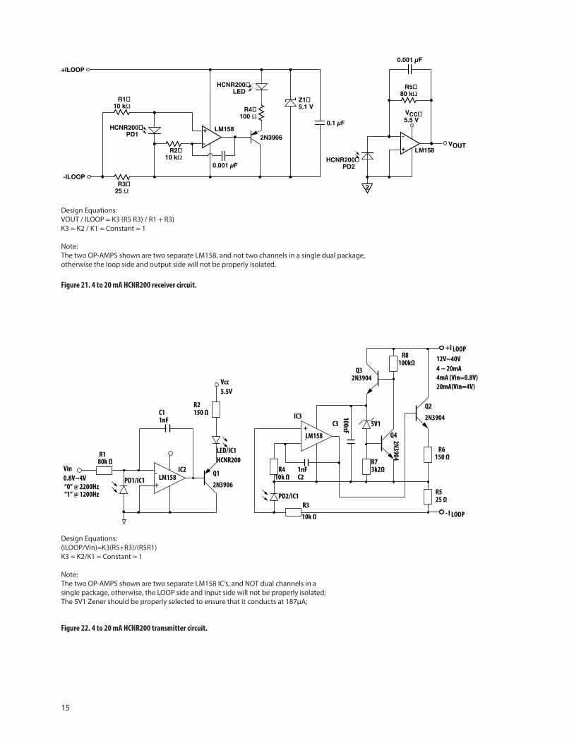
Figure 19. Magnitude/sign isolation amplifier.
-
+VMAG
-
+
VIN OC1PD1
+
-D4
C2 10 pf
C1 10 pf
D3
R4680
OC1LED
R1220 K
C3 10 pf
OC1PD2
R5180 K
R650 K
GAIN
R210 K
R34.7 K
D1
-
+
D2
+
- R76.8 K
VCC
R82.2 K
VIGN
OC26N13
VCC1 +15 VVEE1 -15 V
15
Figure 21. 4 to 20 mA HCNR200 receiver circuit.
Figure 22. 4 to 20 mA HCNR200 transmitter circuit.
-
+VOUT-
+
HCNR200 fig 21
VCC5.5 V
R110 kΩ
+ILOOP
HCNR200PD1
-ILOOP
R210 kΩ
R4100 Ω
2N3906
Z15.1 V
0.1 µF
R325 Ω
0.001 µF
R580 kΩ
LM158HCNR200
PD2
0.001 µF
2
HCNR200LED
LM158
Design Equations:VOUT / ILOOP = K3 (R5 R3) / R1 + R3)K3 = K2 / K1 = Constant = 1
Note: The two OP‑AMPS shown are two separate LM158, and not two channels in a single dual package, otherwise the loop side and output side will not be properly isolated.
Design Equations:(ILOOP/Vin)=K3(R5+R3)/(R5R1)K3 = K2/K1 = Constant ≈ 1
Note: The two OP‑AMPS shown are two separate LM158 IC’s, and NOT dual channels in a single package, otherwise, the LOOP side and input side will not be properly isolated; The 5V1 Zener should be properly selected to ensure that it conducts at 187µA;
-
+
80k Ω
PD1/IC1 LM158IC2
LED/IC1HCNR200
1nF150 Ω
Q1
2N3906
R1
R2
Vcc5.5V
Vin0.8V~4V
C1
-
+
LM158
IC3
PD2/IC1
1nF
10k Ω
25 Ω
10k Ω3k2Ω
5V1
100nF
100kΩ
150 Ω
Q2
Q3
Q4
2N3904
2N3904
2N3904
R3
R4
R5
R6
R7
R8
C2
C3
+I LOOP
- I LOOP
12V~40V4 ~ 20mA4mA (Vin=0.8V)20mA(Vin=4V)
“0” @ 2200Hz“1” @ 1200Hz
16
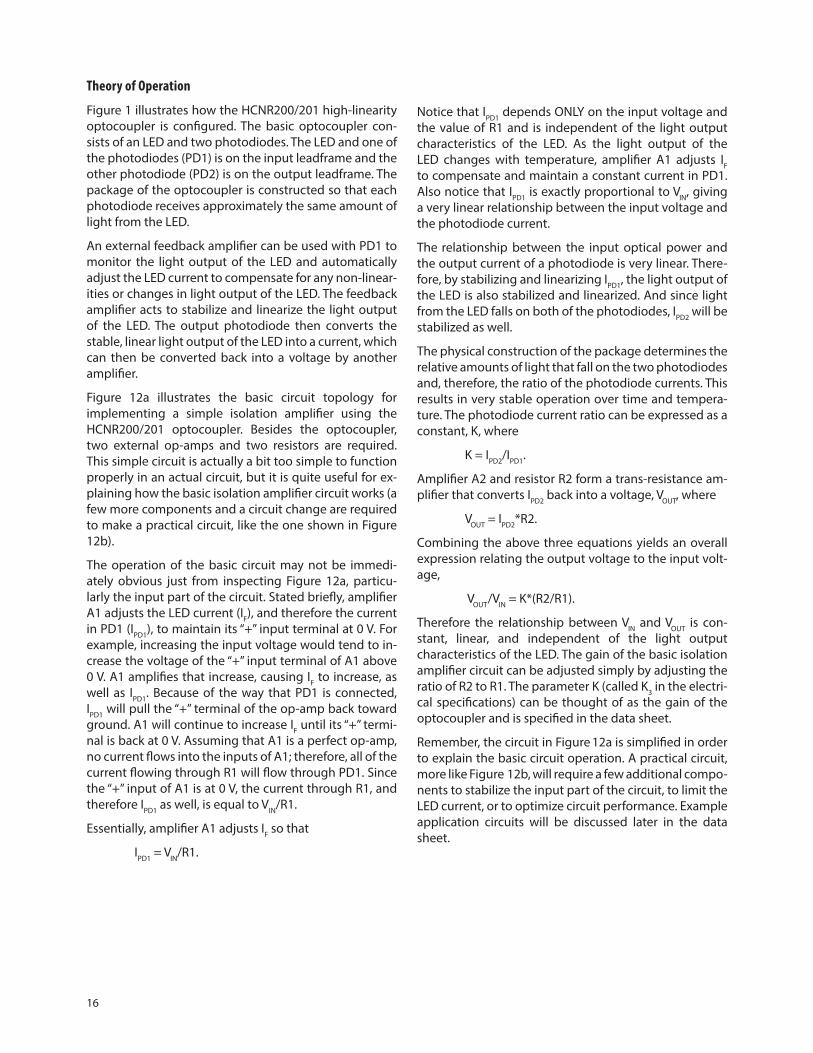
Theory of Operation
Figure 1 illustrates how the HCNR200/201 high‑linearity opto coup ler is configured. The basic optocoupler con‑sists of an LED and two photodiodes. The LED and one of the photodiodes (PD1) is on the input leadframe and the other photodiode (PD2) is on the output leadframe. The package of the optocoupler is constructed so that each photo diode receives approxi mately the same amount of light from the LED.
An external feedback amplifier can be used with PD1 to monitor the light output of the LED and automatically adjust the LED current to compensate for any non‑linear‑ities or changes in light output of the LED. The feedback amplifier acts to stabilize and linearize the light output of the LED. The output photodiode then converts the stable, linear light output of the LED into a current, which can then be converted back into a voltage by another amplifier.
Figure 12a illustrates the basic circuit topology for implement ing a simple isolation amplifier using the HCNR200/201 optocoupler. Besides the optocoupler, two external op‑amps and two resistors are required. This simple circuit is actually a bit too simple to function properly in an actual circuit, but it is quite useful for ex‑plaining how the basic isolation amplifier circuit works (a few more components and a circuit change are required to make a practical circuit, like the one shown in Figure 12b).
The operation of the basic circuit may not be immedi‑ately obvious just from inspecting Figure 12a, particu‑larly the input part of the circuit. Stated briefly, amplifier A1 adjusts the LED current (IF), and therefore the current in PD1 (IPD1), to maintain its “+” input terminal at 0 V. For example, increasing the input voltage would tend to in‑crease the voltage of the “+” input terminal of A1 above 0 V. A1 amplifies that increase, causing IF to increase, as well as IPD1. Because of the way that PD1 is connected, IPD1 will pull the “+” terminal of the op‑amp back toward ground. A1 will continue to increase IF until its “+” termi‑nal is back at 0 V. Assuming that A1 is a perfect op‑amp, no current flows into the inputs of A1; therefore, all of the current flowing through R1 will flow through PD1. Since the “+” input of A1 is at 0 V, the current through R1, and there fore IPD1 as well, is equal to VIN/R1.
Essentially, amplifier A1 adjusts IF so that
IPD1 = VIN/R1.
Notice that IPD1 depends ONLY on the input voltage and the value of R1 and is independent of the light output characteris tics of the LED. As the light output of the LED changes with temperature, ampli fier A1 adjusts IF to compensate and maintain a constant current in PD1. Also notice that IPD1 is exactly proportional to VIN, giving a very linear relationship between the input voltage and the photodiode current.
The relationship between the input optical power and the output current of a photodiode is very linear. There‑fore, by stabiliz ing and linearizing IPD1, the light output of the LED is also stabilized and linearized. And since light from the LED falls on both of the photodiodes, IPD2 will be stabilized as well.
The physical construction of the package determines the relative amounts of light that fall on the two photodiodes and, therefore, the ratio of the photodiode currents. This results in very stable operation over time and tempera‑ture. The photodiode current ratio can be expressed as a constant, K, where
K = IPD2/IPD1.
Amplifier A2 and resistor R2 form a trans‑resistance am‑plifier that converts IPD2 back into a voltage, VOUT, where
VOUT = IPD2*R2.
Combining the above three equations yields an overall expression relating the output voltage to the input volt‑age,
VOUT/VIN = K*(R2/R1).
Therefore the relationship between VIN and VOUT is con‑stant, linear, and independent of the light output characteris tics of the LED. The gain of the basic isola tion amplifier circuit can be adjusted simply by adjusting the ratio of R2 to R1. The parameter K (called K3 in the electri‑cal specifications) can be thought of as the gain of the optocoupler and is specified in the data sheet.
Remember, the circuit in Figure 12a is simplified in order to explain the basic circuit opera tion. A practical circuit, more like Figure 12b, will require a few additional compo‑nents to stabilize the input part of the circuit, to limit the LED current, or to optimize circuit performance. Example applica tion circuits will be discussed later in the data sheet.
17
to worry about. How ever, the second circuit requires two optocouplers, separate gain adjustments for the posi‑tive and negative portions of the signal, and can exhibit crossover distor tion near zero volts. The correct circuit to choose for an applica tion would depend on the require‑ments of that particular application. As with the basic isolation amplifier circuit in Figure 12a, the circuits in Fig‑ure 14 are simplified and would require a few additional compo nents to function properly. Two example circuits that operate with bipolar input signals are discussed in the next section.
As a final example of circuit design flexibility, the simpli‑fied schematics in Figure 15 illus trate how to implement 4‑20 mA analog current‑loop transmitter and receiver circuits using the HCNR200/201 optocoupler. An impor‑tant feature of these circuits is that the loop side of the circuit is powered entirely by the loop current, eliminat‑ing the need for an isolated power supply.
The input and output circuits in Figure 15a are the same as the negative input and positive output circuits shown in Figures 13c and 13b, except for the addition of R3 and zener diode D1 on the input side of the circuit. D1 regu‑lates the supply voltage for the input amplifier, while R3 forms a current divider with R1 to scale the loop current down from 20 mA to an appropriate level for the input circuit (<50 µA).
As in the simpler circuits, the input amplifier adjusts the LED current so that both of its input terminals are at the same voltage. The loop current is then divided
between R1 and R3. IPD1 is equal to the current in R1 and is given by the following equation:
IPD1 = ILOOP*R3/(R1+R3).
Combining the above equation with the equations used for Figure 12a yields an overall expression relating the output voltage to the loop current,
VOUT/ILOOP = K*(R2*R3)/(R1+R3).
Again, you can see that the relationship is constant, lin‑ear, and independent of the charac teristics of the LED.
The 4‑20 mA transmitter circuit in Figure 15b is a little dif‑ferent from the previous circuits, partic ularly the output circuit. The output circuit does not directly generate an output voltage which is sensed by R2, it instead uses Q1 to generate an output current which flows through R3. This output current generates a voltage across R3, which is then sensed by R2. An analysis similar to the one above yields the following expression relating output current to input voltage:
ILOOP/VIN = K*(R2+R3)/(R1*R3).
Circuit Design Flexibility
Circuit design with the HCNR200/201 is very flexible because the LED and both photodiodes are acces sible to the designer. This allows the designer to make perf‑ormance trade‑offs that would otherwise be difficult to make with commercially avail able isolation amplifiers (e.g., band width vs. accuracy vs. cost). Analog isola tion circuits can be designed for applications that have either unipolar (e.g., 0‑10 V) or bipolar (e.g., ±10 V) signals, with positive or negative input or output voltages. Several simplified circuit topologies illustrating the design flex‑ibility of the HCNR200/201 are discussed below.
The circuit in Figure 12a is configured to be non‑invert‑ing with positive input and output voltages. By simply changing the polarity of one or both of the photodiodes, the LED, or the op‑amp inputs, it is possible to imple ment other circuit configu ra tions as well. Figure 13 illustrates how to change the basic circuit to accommodate both positive and negative input and output voltages. The in‑put and output circuits can be matched to achieve any combina tion of positive and negative voltages, allowing for both inverting and non‑inverting circuits.
All of the configurations described above are unipolar (single polar ity); the circuits cannot accom mo date a sig‑nal that might swing both positive and negative. It is pos‑sible, however, to use the HCNR200/201 optocoupler to implement a bipolar isolation amplifier. Two topologies that allow for bipolar operation are shown in Figure 14.
The circuit in Figure 14a uses two current sources to offset the signal so that it appears to be unipolar to the optocoupler. Current source IOS1 provides enough offset to ensure that IPD1 is always positive. The second current source, IOS2, provides an offset of opposite polarity to ob‑tain a net circuit offset of zero. Current sources IOS1 and IOS2 can be implemented simply as resistors connected to suitable voltage sources.
The circuit in Figure 14b uses two optocouplers to obtain bipolar operation. The first optocoupler handles the pos‑itive voltage excursions, while the second optocoupler handles the negative ones. The output photo diodes are connected in an antiparallel configuration so that they produce output signals of opposite polarity.
The first circuit has the obvious advantage of requiring only one optocoupler; however, the offset performance of the circuit is dependent on the matching of IOS1 and IOS2 and is also dependent on the gain of the optocoupler. Changes in the gain of the opto coupler will directly af‑fect the offset of the circuit.
The offset performance of the second circuit, on the other hand, is much more stable; it is inde pendent of optocoupler gain and has no matched current sources
18
The preceding circuits were pre sented to illustrate the flexibility in designing analog isolation circuits using the HCNR200/201. The next section presents several com‑plete schematics to illustrate practical applications of the HCNR200/201.
Example Application Circuits
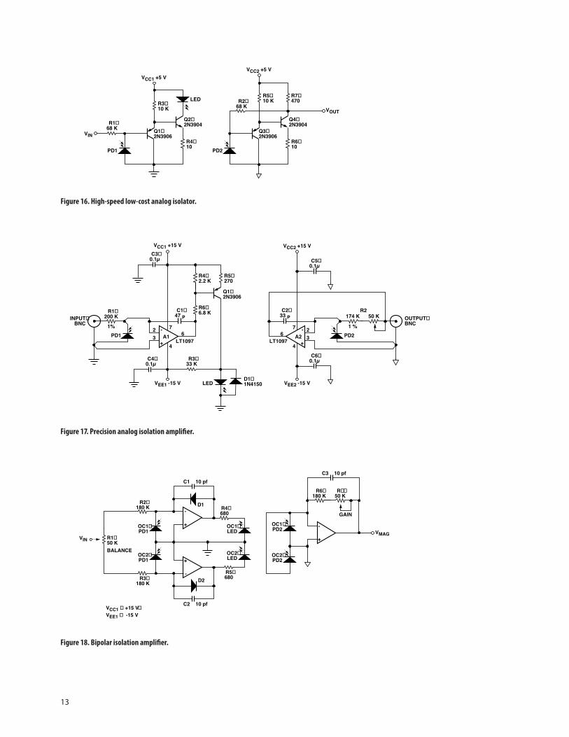
The circuit shown in Figure 16 is a high‑speed low‑cost circuit designed for use in the feedback path of switch‑mode power supplies. This application requires good bandwidth, low cost and stable gain, but does not re‑quire very high accuracy. This circuit is a good example of how a designer can trade off accuracy to achieve improve ments in bandwidth and cost. The circuit has a bandwidth of about 1.5 MHz with stable gain character‑istics and requires few external components.
Although it may not appear so at first glance, the circuit in Figure 16 is essentially the same as the circuit in Fig‑ure 12a. Amplifier A1 is comprised of Q1, Q2, R3 and R4, while amplifier A2 is comprised of Q3, Q4, R5, R6 and R7. The circuit operates in the same manner as well; the only difference is the performance of amplifiers A1 and A2. The lower gains, higher input currents and higher offset voltages affect the accuracy of the circuit, but not the way it operates. Because the basic circuit operation has not changed, the circuit still has good gain stability. The use of discrete transistors instead of op‑amps allowed the design to trade off accuracy to achieve good band‑width and gain stability at low cost.
To get into a little more detail about the circuit, R1 is se‑lected to achieve an LED current of about 7‑10 mA at the nominal input operating voltage according to the fol‑lowing equation:
IF = (VIN/R1)/K1,
where K1 (i.e., IPD1/IF) of the optocoupler is typically about 0.5%. R2 is then selected to achieve the desired output volt age according to the equation,
VOUT/VIN = R2/R1.
The purpose of R4 and R6 is to improve the dynamic re‑sponse (i.e., stability) of the input and output circuits by lowering the local loop gains. R3 and R5 are selected to provide enough current to drive the bases of Q2 and Q4. And R7 is selected so that Q4 operates at about the same collector current as Q2.
The next circuit, shown in Figure 17, is designed to achieve the highest possible accuracy at a reasonable cost. The high accuracy and wide dynamic range of the circuit is achieved by using low‑cost precision op‑amps with very low input bias currents and offset voltages and is limited by the performance of the opto coupler. The circuit is de‑signed to operate with input and output voltages from 1 mV to 10 V.
The circuit operates in the same way as the others. The only major differences are the two compensa tion capaci‑tors and additional LED drive circuitry. In the high‑speed circuit discussed above, the input and output circuits are stabilized by reducing the local loop gains of the input and output circuits. Because reducing the loop gains would decrease the accuracy of the circuit, two compen‑sation capacitors, C1 and C2, are instead used to improve circuit stability. These capacitors also limit the bandwidth of the circuit to about 10 kHz and can be used to reduce the output noise of the circuit by reducing its bandwidth even further.
The additional LED drive circuitry (Q1 and R3 through R6) helps to maintain the accuracy and band width of the circuit over the entire range of input voltages. Without these components, the transcon duc t ance of the LED driver would decrease at low input voltages and LED currents. This would reduce the loop gain of the input circuit, reducing circuit accuracy and bandwidth. D1 pre‑vents excessive reverse voltage from being applied to the LED when the LED turns off completely.
No offset adjustment of the circuit is necessary; the gain can be adjusted to unity by simply adjusting the 50 kohm poten tiometer that is part of R2. Any OP‑97 type of op‑amp can be used in the circuit, such as the LT1097 from Linear Technology or the AD705 from Analog Devices, both of which offer pA bias currents, µV offset voltages and are low cost. The input terminals of the op‑amps and the photodiodes are connected in the circuit using Kelvin connections to help ensure the accuracy of the circuit.
The next two circuits illustrate how the HCNR200/201 can be used with bipolar input signals. The isolation amplifier in Figure 18 is a practical implemen tation of the circuit shown in Figure 14b. It uses two opto couplers, OC1 and OC2; OC1 handles the positive portions of the input sig‑nal and OC2 handles the negative portions.
Diodes D1 and D2 help reduce crossover distortion by keeping both amplifiers active during both positive and negative portions of the input signal. For example, when the input signal positive, optocoupler OC1 is active while OC2 is turned off. However, the amplifier control ling OC2 is kept active by D2, allowing it to turn on OC2 more rap‑idly when the input signal goes negative, thereby reduc‑ing crossover distortion.
Balance control R1 adjusts the relative gain for the posi‑tive and negative portions of the input signal, gain con‑trol R7 adjusts the overall gain of the isolation amplifier, and capac i tors C1‑C3 provide compensa tion to stabilize the amplifiers.

For product information and a complete list of distributors, please go to our website: www.avagotech.com
Avago, Avago Technologies, and the A logo are trademarks of Avago Technologies in the United States and other countries.Data subject to change. Copyright © 2005-2014 Avago Technologies. All rights reserved. Obsoletes AV01-0567ENAV02-0886EN - July 1, 2014
The final circuit shown in Figure 19 isolates a bipolar analog signal using only one optocoupler and generates two output signals: an analog signal proportional to the magnitude of the input signal and a digital signal cor‑responding to the sign of the input signal. This circuit is especially useful for applica tions where the output of the circuit is going to be applied to an analog‑to‑digital converter. The primary advantages of this circuit are very good linearity and offset, with only a single gain adjust‑ment and no offset or balance adjustments.
To achieve very high linearity for bipolar signals, the gain should be exactly the same for both positive and negative input polarities. This circuit achieves excellent linearity by using a single optocoupler and a single input resistor, which guarantees identical gain for both posi‑tive and negative polarities of the input signal. This pre‑cise matching of gain for both polari ties is much more difficult to obtain when separate components are used for the different input polari ties, such as is the pre vious circuit.
The circuit in Figure 19 is actually very similar to the pre‑vious circuit. As mentioned above, only one optocoupler is used. Because a photodiode can conduct current in only one direction, two diodes (D1 and D2) are used to steer the input current to the appropriate terminal of input photodiode PD1 to allow bipolar input currents. Normally the forward voltage drops of the diodes would cause a serious linearity or accuracy problem. However, an additional amplifier is used to provide an appropriate offset voltage to the other amplifiers that exactly cancels the diode voltage drops to maintain circuit accuracy.
Diodes D3 and D4 perform two different functions; the diodes keep their respective amplifiers active indepen‑dent of the input signal polarity (as in the previous cir‑cuit), and they also provide the feedback signal to PD1 that cancels the voltage drops of diodes D1 and D2.
Either a comparator or an extra op‑amp can be used to sense the polarity of the input signal and drive an inex‑pensive digital optocoupler, like a 6N139.
It is also possible to convert this circuit into a fully bipolar circuit (with a bipolar output signal) by using the output of the 6N139 to drive some CMOS switches to switch the polarity of PD2 depending on the polarity of the input signal, obtaining a bipolar output voltage swing.
HCNR200/201 SPICE Model
Figure 20 is the net list of a SPICE macro‑model for the HCNR200/201 high‑linearity optocoupler. The macro‑model accurately reflects the primary characteristics of the HCNR200/201 and should facilitate the design and understanding of circuits using the HCNR200/201 opto‑coupler.
Related Documents