HCD-DR3/DR330/XB200 AEP Model UK Model HCD-XB200 E Model HCD-DR3/DR330 Australian Model HCD-DR3 SERVICE MANUAL Continued on next page SPECIFICATIONS COMPACT Hi-Fi STEREO SYSTEM SPECIFICATIONS HCD-DR3/DR330/XB200 are the tuner, deck, CD and amplifier section in LBT-DR3/ DR330/XB200. Model Name Using Similar Mechanism HCD-G2500 Base Unit Type KSM-213ECM Optical Pick-up Type KSS-213E Model Name Using Similar Mechanism NEW Tape Transport Mechanism Type CWL-44-RR CD SECTION TAPE DECK SECTION Manufactured under license from Dolby Laboratories Licensing Corporation. “DOLBY” and the double-D symbol aare trademarks of Dolby Laboratories Licensing Corporation. Ver 1.1 2001.10 Sony Corporation Home Audio Company Published by Sony Engineering Corporation 9-928-976-12 2001J1600-1 © 2001.10 Amplifier section (LBT-XB200) DIN power output (Rated) 70W + 70W (6 Ω at 1 kHz DIN) Continuous RMS power output (Reference) 80W + 80W (6 Ω at 1 kHz, 10% THD) Music power output (Reference) 140W + 140W (6 Ω at 1 kHz, 10% THD) (LBT-DR330/DR3) The following measured at AC 110/220V, 60Hz ; Continuous RMS power output (Reference) 85W + 85W (6 Ω at 1 kHz, 10% THD) DIN power output (Rated) 70W + 70W (6 Ω at 1 kHz, DIN) The following measured at AC 120/240V, 60Hz ; Continuous RMS power output (Reference) 100W + 100W (6 Ω at 1 kHz, 10% THD) DIN power output (Rated) 80W + 80W (6 Ω at 1 kHz, DIN) Inputs PHONO IN (phono jack): sensitivity 3mV, impedance 47 kΩ MD/VIDEO IN (phono jacks): sensitivity 250mV, impedance 47 kΩ Outputs PHONOS (stereo phono jacks): accepts headphones of 8 Ω or more MD/VIDEO OUT (phone jack): voltage 250mV, impedance 1 kΩ SPEAKER: accepts impedance of 6 to 16 Ω CD player section System Compact disc and digital audio system Laser Semiconductor laser (λ = 780 nm) Emission duration: continuous Laser output Max. 44.6µW* *This output is the value measured at a distance of 200 mm from the objective lens surface on the Optical Pock-up Block with 7 mm aperture. Wavelength 780 – 790 nm Frequency response 20Hz – 20kHz (±0.5 dB) Signal-to-noise retio More than 90 dB Dynamic range More than 90 dB DIGITAL OUT (Square optical connector jack, rear panel) Wavelength 600 nm Output Level –18 dBm Tape deck section Recording system 4-track 2-channel stereo Frequency response (DOLBY NR OFF) 60 – 13,000 Hz (±3 dB), using a Sony TYPE I cassette Tuner section FM stereo, FM/AM superheterodyne tuner FM tunr section Tuning range 87.5 – 108.0 MHz (50 kHz step)

Welcome message from author
This document is posted to help you gain knowledge. Please leave a comment to let me know what you think about it! Share it to your friends and learn new things together.
Transcript

HCD-DR3/DR330/XB200AEP Model
UK ModelHCD-XB200
E ModelHCD-DR3/DR330
Australian ModelHCD-DR3
SERVICE MANUAL
Continued on next page
SPECIFICATIONS
COMPACT Hi-Fi STEREO SYSTEM
SPECIFICATIONS
HCD-DR3/DR330/XB200 are the tuner,deck, CD and amplifier section in LBT-DR3/DR330/XB200.
Model Name Using Similar Mechanism HCD-G2500
Base Unit Type KSM-213ECM
Optical Pick-up Type KSS-213E
Model Name Using Similar Mechanism NEW
Tape Transport Mechanism Type CWL-44-RR
CD
SECTION
TAPEDECK
SECTION
Manufactured under license from Dolby LaboratoriesLicensing Corporation.“DOLBY” and the double-D symbol a are trademarksof Dolby Laboratories Licensing Corporation.
Ver 1.1 2001.10
Sony CorporationHome Audio Company
Published by Sony Engineering Corporation
9-928-976-122001J1600-1
© 2001.10
Amplifier section(LBT-XB200)DIN power output (Rated) 70W + 70W
(6 Ω at 1 kHz DIN)Continuous RMS power output (Reference)
80W + 80W(6 Ω at 1 kHz, 10%THD)
Music power output (Reference)140W + 140W(6 Ω at 1 kHz, 10%THD)
(LBT-DR330/DR3)The following measured at AC 110/220V, 60Hz ;Continuous RMS power output (Reference)
85W + 85W(6 Ω at 1 kHz, 10%THD)
DIN power output (Rated) 70W + 70W(6 Ω at 1 kHz, DIN)
The following measured at AC 120/240V, 60Hz ;Continuous RMS power output (Reference)
100W + 100W(6 Ω at 1 kHz, 10%THD)
DIN power output (Rated) 80W + 80W(6 Ω at 1 kHz, DIN)
InputsPHONO IN (phono jack):
sensitivity 3mV,impedance 47 kΩ
MD/VIDEO IN (phono jacks):sensitivity 250mV,impedance 47 kΩ
OutputsPHONOS (stereo phono jacks):
accepts headphones of 8 Ωor more
MD/VIDEO OUT (phone jack):voltage 250mV,impedance 1 kΩ
SPEAKER: accepts impedance of 6 to16 Ω
CD player sectionSystem Compact disc and digital
audio systemLaser Semiconductor laser
(λ = 780 nm)Emissionduration: continuous
Laser output Max. 44.6µW**This output is the valuemeasured at a distance of200 mm from the objectivelens surface on the OpticalPock-up Block with 7 mmaperture.
Wavelength 780 – 790 nmFrequency response 20Hz – 20kHz (±0.5 dB)Signal-to-noise retio More than 90 dBDynamic range More than 90 dBDIGITAL OUT(Square optical connector jack, rear panel)Wavelength 600 nmOutput Level –18 dBm
Tape deck sectionRecording system 4-track 2-channel stereoFrequency response (DOLBY NR OFF)
60 – 13,000 Hz (±3 dB),using a Sony TYPE Icassette
Tuner sectionFM stereo, FM/AM superheterodyne tuner
FM tunr sectionTuning range 87.5 – 108.0 MHz
(50 kHz step)

2
SAFETY-RELATED COMPONENT WARNING!!
COMPONENTS IDENTIFIED BY MARK ! OR DOTTED LINE WITHMARK ! ON THE SCHEMATIC DIAGRAMS AND IN THE PARTSLIST ARE CRITICAL TO SAFE OPERATION. REPLACE THESECOMPONENTS WITH SONY PARTS WHOSE PART NUMBERSAPPEAR AS SHOWN IN THIS MANUAL OR IN SUPPLEMENTSPUBLISHED BY SONY.
This appliance is classified as a CLASS 1 LASER product. TheCLASS 1 LASER PRODUCT MARKING is located on the rearexterior.
The following caution label is located inside the unit.
Laser component in this product is capableof emitting radiation exceeding the limit forClass 1.
CAUTIONUse of controls or adjustments or performance of proceduresother than those specified herein may result in hazardous radiationexposure.
Notes on chip component replacement• Never reuse a disconnected chip component.• Notice that the minus side of a tantalum capacitor may be
damaged by heat.
Flexible Circuit Board Repairing• Keep the temperature of soldering iron around 270˚C
during repairing.• Do not touch the soldering iron on the same conductor of the
circuit board (within 3 times).• Be careful not to apply force on the conductor when soldering
or unsoldering.
AM tuner sectionTuning renge
European and Middle Eastern models:531 – 1,602 kHz(with the tuning interval set at 9 kHz)
Other models: 531 – 1,602 kHz(with the tuning interval set at 9 kHz)530 – 1,710 kHz(with the tuning interval set at 10 kHz)
Antenna AM loop antenna,External antenna terminals
Intermediate frequency 450 kHz
GeneralPower requirements
European model: 230 V AC, 50/60 HzMexican model: 120V AC, 50/60 HzAustralian model: 220 – 240 V AC, 50/60 HzOther models: 110 – 120 V or 220 – 240 V AC, 50/60 Hz Adjustable
with voltage selectorPower consumption(HCD-DR330/DR3) 180W(HCD-XB200) 135WDimensions(w/h/d) Approx. 355 × 425 × 442 mm
(14 × 163/4 × 171/2 in) incl.projecting parts and controls
Mass Approx. 13.1 kg (28 lb 14 oz.)
Supplied accessories AM loop antenna (1)Remote RM-SG7B (1)FM wire antenna (1)
Design and specifications are subject to change without notice
Parts No.
PARTS No. MODEL4-222-140-0π XB200 : AEP, UK
4-222-141-0π XB200 : EE, CIS
4-222-142-0π DR3 : E, SP, AR
4-222-143-0π DR3 : AUS
4-222-144-0π DR3 : MX
4-222-145-0π DR330
MODEL IDENTIFICATION
• AbbreviationSP : Singapore modelMX : Mexican modelAR : Argentina modelAUS : Australian modelEE : East European model

3
1. GENERAL ·········································································· 4
2. DISASSEMBLY2-1. Top Cover ··········································································· 52-2. Front Panel Assy ································································· 52-3. Main Section······································································· 62-4. Main Board ········································································· 62-5. CD Mechanism Deck Section ············································ 72-6. Tape Mechanism Deck Section ·········································· 72-7. Cassette Doors ···································································· 82-8. CD Chassis Assy ································································ 82-9. Base Unit ············································································ 92-10. Turn Table ··········································································· 9
3. MECHANICAL ADJUSTMENTS ····························· 10
4. ELECTRICAL ADJUSTMENTS ······························· 10
5. DIAGRAMS5-1. Ciecuit Boards Location ··················································· 155-2. Block Diagrams ································································ 16
Main Section····································································· 16Tuner/CD Section ····························································· 17
5-3. Printed Wiring Board Main Section ····························· 185-4. Schematic Diagram Main (1/3) Section ······················· 195-5. Schematic Diagram Main (2/3) Section ······················· 205-6. Schematic Diagram Main (3/3) Section ······················· 215-7. Printed Wiring Board AMP Section ····························· 225-8. Schematic Diagram AMP Section ································ 235-9. Printed Wiring Board CD Decoder Section ················· 245-10. Schematic Diagram CD Decoder Section ···················· 255-11. Printed Wiring Board Front Section ····························· 265-12. Schematic Diagram Front (1/2) Section ······················· 275-13. Schematic Diagram Front (2/2) Section ······················· 285-14. IC Pin Function Description ············································· 295-15. IC Block Diagrams ··························································· 31
6. EXPLODED VIEWS6-1. Top Cover Section ···························································· 336-2. CD Door Section ······························································ 346-3. Panel Section ···································································· 356-4. Main Section····································································· 366-5. CD Mechanism Section ···················································· 376-6. Base Unit Section (KSM-213ECM) ································· 38
7. ELECTRICAL PARTS LIST ······································· 39
TABLE OF CONTENTS

4
1 1/u (POWER) button2 TUNING MODE button3 STEREO/MONO button4 TUNER MEMORY button5 ENTER/NEXT button6 TUNER/BAND button7 TUNING – button8 TUNING + button9 FUNCTION button!º VOLUME knob!¡ PHONES jack!™ ª button (DECK B)!£ · button (DECK B)!¢ p button (DECK B)!∞ 0 button (DECK B)!§ ) button (DECK B)!¶ P button (DECK B)!• r REC button (DECK B)
!ª CD SYNCHRO button@º 0 button (CD)@¡ ) button (CD)@™ fl button (CD)@£ p button (CD)@¢ REPEAT button@∞ PLAY MODE button@§ AMS knob@¶ DISC SKIP button@• EDIT button@ª DISC 5 button#º DISC 4 button#¡ DISC 3 button#™ DISC 2 button#£ DISC 1 button#¢ DIRECTION button#∞ DOLBY NR button#§ p button (DECK A)
SECTION 1GENERAL
#¶ 0 button (DECK A)#• ) button (DECK A)#ª ª button (DECK A)$º · button (DECK A)$¡ GROOVE button$™ DBFB button$£ SURROUND button$¢ SPECTRUM ANALYZER button$∞ DISPLAY/DEMO button$§ ROCK button$¶ POPS button$• JAZZ button$ª SALSA button%º FLAT button%¡ t /CLOCK SET button%™ SLEEP button%£ TIMER REC button%¢ DAILY button
1 %¢ %£ 23 54$ª $• %º 6
8
9
7
!¡
%™ %¡
#™
#£
@™
0
$∞ $¢
!£ !™
$¶ $§
$º #ª
$™ $¡ $£
@¡ @º
!• !ª
@£
!¶
!§ !∞ !¢
@∞ @¶ #º #¡ @¢ @§ @• @ª
#∞ #¢
#¶ #§ #•

5
SECTION 2DISASSEMBLY
Note : Follow the disassembly procedure in the numerical order given.
2-1. TOP COVER
2-2. FRONT PANEL ASSY
2 Seven screws
1 Three screws
1 Three screws
3 Top cover
9 Front panel assy
6 Four screws
7 Screw
1 Connector (to deck A)2 Harness
(CN302)
4 Connector (to deck B)
5 Connector (CN702)
8 Board to board connector (CN602) (CN601)
3 Connector board (CN11)

6
2-3. MAIN SECTION
2-4. MAIN BOARD
5 Two screws
4 Three screws
6 Two screws
7 Main section
2 Screw
3 Photo Socket board
1 Connector (CN301)
4 Three screws
3 Four screws
1 Four screws
2 Three screws
5 Rear panel
6 Connector (CN701)
8 Main board
7 Two screws

7
2-5. CD MECHANISM DECK SECTION
2-6. TAPE MECHANISM DECK
3 Four screws
4 CD mechanism deck section
2 Holder, wire
1 Two screws
2 Six screws 1 Flexible flat cable (to connector 16pin on tape mechanism deck)
3 Tape mechanism deck

8
2-7. CASSETTE DOORS
2-8. CD CHASSIS ASSY
Cassette door (R)(Note: Four claws are used.)
Cassette door (L)(Note: Four claws are used.)
1 Connector (CN603)
8 Three screws
5 AMS knob
7 Washer
6 Nut
!º Three screws
!¡ CD key board
!™ CD chassis assy
9 AMS board
3 Five screws
2 Connector (CN606)
4 Remove the six claws

9
2-9. BASE UNIT
2-10. TURN TABLE
Note:When the disc table is installed, adjust the positions ofroller can and mark ” as shown in the figure, then setto the groove of disc table.
5 Base unit
3 Yoke bracket
1 Connector (CN02)
2 Connector (CN01)
4 Boss
1 Screw
1 Screw4 Turn table
3 Step screw
2 Bracket (BU)
A
A

10
2. Turn the adjustment screw and check output peaks. If the peaksdo not match for L-CH and R-CH, turn the adjustment screwso that outputs match within 2 dB of peak.
L-CHpeak
R-CHpeak
screwposition
outputlevel within
2dB
L-CHpeak
R-CHpeak
screwposition
within 2dB
Precaution1. Clean the following parts with a denatured alcohol-moistened
swab:record/playback head pinch rollerserase head rubber beltscapstan idlers
2. Demagnetize the record/playback head with a headdemagnetizer.
3. Do not use a magnetized screwdriver for the adjustments.4. After the adjustments, apply suitable locking compound to the
parts adjusted.5. The adjustments should be performed with the rated power
supply voltage unless otherwise noted.
Torque Measurement
SECTION 3MECHANICAL ADJUSTMENTS
Meter reading40 to 70 g • cm
(0.56 - 0.97 oz • inch)
1 to 5 g • cm(0.01 - 0.07 oz • inch)
55 to 140 g • cm(0.76 - 1.94 oz • inch)
Torque
FWD
FWDback tension
FF/REW
Torque meter
CQ-102C
CQ-102C
CQ-201B
SECTION 4ELECTRICAL ADJUSTMENTS
1. Demagnetize the record/playback head with a headdemagnetizer.
2. Do not use a magnetized screwdriver for the adjustments.3. After the adjustments, apply suitable locking compound to the
parts adjusted.4. The adjustments should be performed with the rated power
supply voltage unless otherwise noted.5. The adjustments should be performed in the order given in this
service manual. (As a general rule, playback circuit adjustmentshould be completed before performing recording circuitadjustment.)
6. The adjustments should be performed for both L-CH and R-CH.
Record/Playback Head Azimuth Adjustment(Deck A, Deck B)
Note: Perform this adjustments for both decks.
Procedure:1. Mode : Playback
DECK SECTION 0 dB=0.775V
TapeP-4-A100
WS-48B
Signal10 kHz, –10 dB
3 kHz, 0 dB
Used forAzimuth Adjustment
Tape Speed Adjustment
test tapeP-4-A100(10kHz, –10dB)
set
SPEAKERterminal (JK703)
level meter

11
test tapeP-4-A100(10kHz, –10dB)
SPEAKERterminal (JK703)(L-CH)
SPEAKERterminal (JK703)(R-CH)
oscilloscope
L
R
Waveform of oscilloscope
in phase 45˚ 90˚ 135˚ 180˚
good wrong
test tapeWS-48B(3kHz, 0dB)
set
SPEAKERterminal (JK703)
frequency counter
+–
IC603
CN603
SFR601
TAPE SPEED
Adjustment screwsPB head (deckA)or REC/PB head (deck B)
3. Mode: Playback Tape Speed Adjustment (Deck A)
Procedure:1. Mode: Playback
2. Adjust the SFR601 so that the frequency counter reads 3,000Hz ± 90Hz.
Adjustment Location: FRONT board
Sample Value of Wow and flutterW. RMS (JIS) within 0.3%(test tape: WS-48B)
Adjustment Location: FRONT board[FRONT BOARD] — Component side —4. After the adjustments, apply suitable locking compound to the
parts adjusted.
Adjustment Location:Remove the cassette lid before adjustment (See page 8)

12
TUNER SECTION 0 dB=1µV
AM Tuning Voltage Adjustment
Procedure:1. Set the reception frequency of the unit to 530 kHz.2. Adjust L105 for 1.2 ± 0.05 V reading on the DC voltmeter.3. Set the reception frequency of the unit to 1,710 kHz.4. Confirm that the voltage reading on the DC voltmeter is within
8.0 ± 0.5 V.
Adjustment Location: MAIN board (See page 13)
AM Tracking Adjustment
Procedure:1. Tune the set to 600 kHz.2. Set the output of AM RF SSG so that the input level of the set
will become 60 dB (µV/m).3. Adjust L104 so that when the waveform on the oscilloscope is
maximum, no noise appears.4. Tune the set to 1,400 kHz.
5. Adjust TC102 so that when the waveform on the oscilloscopeis maximum, no noise appears.
• Repeat the procedures in each adjustment several times, and thetracking adjustment should be finally done by the trimmercapacitors.
Adjustment Location: MAIN board (See page 13)
Main boardTP1
GVT
DC voltmeter
+
–
AM RF SSG
loop antenna
set
loop antenna(Supplied accessories)
60 cm AM ANTENNAterminal (TM1)30% amplitude
modulation by400 Hz signal Field strength dB (µV/m) =SSG output level dB (µV/m) –26 dB.

13
FM Tuned Level Adjustment
Procedure:1. Supply a 28 dB 98 MHz signal from the ANTENNA terminal.2. Tune the set to 98 MHz.3. Adjust SFR101 to the point (moment) when the TUNED
indicator will change from going off to going on.
Adjustment Location: MAIN board
Adjustment Location
[MAIN BOARD] — Component side —
FM RF SSG
75 Ω coaxial
Carrier frequency : 98 MHzModulation : AUDIO 1 kHz, 75 kHz deviation (100%)Output level : 28 dB (at 75 W open)
FM ANTENNA terminal(JK101)
set
L104
L105
TP1
TC102
AM Tracking
AM Tuning Voltage
FM Tuned Level
IC102
SFR101JK101
14
CD SECTION
Note:1. CD Block is basically constructed to operate without
adjustment. Therefore, check each item in order given.2. Use YEDS-18 disc (3-702-101-01) unless otherwise indicated.3. Use an oscilloscope with more than 10MΩ impedance.4. Clean the object lens by an applicator with neutral detergent
when the signal level is low than specified value with thefollowing checks.
5. Adjust the focus bias adjustment when optical pick-up block isreplaced.
RF Level Check
Procedure :1. Connect oscilloscope to test point TP01 on CD DECODER
board.2. Turned Power switch on.3. Put disc (YEDS-18) in and playback.4. Confirm that oscilloscope waveform is clear and check RF
signal level is correct or not.Note: Clear RF signal waveform means that the shape “◊” can be
clearly distinguished at the center of the waveform.
Adjustment Location:
[CD DECODER BOARD] — Component side —
CD DECODERboard
oscilloscope
RFVC
TP01
VOLT/DIV: 200 mVTIME/DIV: 500 nS
level: 1.0 Vp-p+0.3–0.2
TP01(VC)
1515
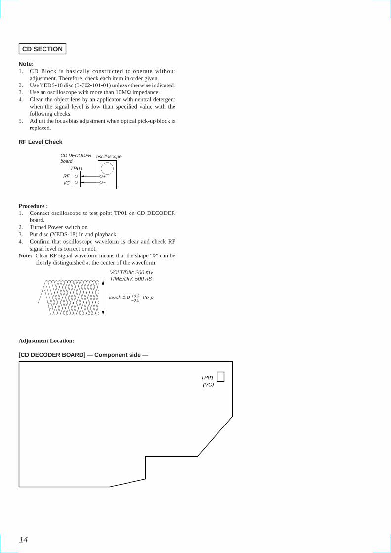
SECTION 5DIAGRAMS
5-1. CIRCUIT BOARDS LOCATION • Waveform
1
2
3
4
IC103 @™
IC601 !§
IC01 #£
IC02 &¡
5 L809 5
6 L809 6
3.6 Vp-p7.2 MHz
3.8 Vp-p6 MHz
1.3 Vp-p
5.0 Vp-p16.9345 MHz
32 Vp-p111.7 kHz
96 Vp-p111.0 kHz
MAIN BOARD
FRONT BOARD
CD DECODE BOARD
For schematic diagrams.Note:• All capacitors are in µF unless otherwise noted. pF: µµF
50 WV or less are not indicated except for electrolyticsand tantalums.
• All resistors are in Ω and 1/4 W or less unless otherwisespecified.
• % : indicates tolerance.• ¢ : internal component.• 2 : nonflammable resistor.• 1 : fusible resistor.• C : panel designation.
• U : B+ Line.• V : B– Line.• H : adjustment for repair.• Voltages and waveforms are dc with respect to ground
under no-signal (detuned) conditions.• Voltages are taken with a VOM (Input impedance 10 MΩ).
Voltage variations may be noted due to normal produc-tion tolerances.
• Waveforms are taken with a oscilloscope.• Circled numbers refer to waveforms.• Signal path.F : FMf : AME : PB (DECK A)d : PB (DECK B)G : REC (DECK B)J : CDg : MD/VIDEOi : PHONO
For printed wiring boards.Note:• X : parts extracted from the component side.• ® : Through hole.• ¢ : internal component.• b : Pattern from the side which enables seeing.
THIS NOTE IS COMMON FOR PRINTED WIRINGBOARDS AND SCHEMATIC DIAGRAMS.(In addition to this necessary note is printed in eachblock.)
• Indication of transistor.
• AbbreviationSP : Singapore modelMX : Mexican modelAR : Argentina modelAUS : Australian model
MAIN board
CONNECTOR board
TR board
LED board
CD KEY board
CD SW board
POWER (AMP) board
POWER SUPPLY board
AC SWITCH board
PHOTO SOCKET board
REM board
AMS board
VR board
H/P board
FRONT board
MOTOR board
DISC NO board CD DECODE board
MOTOR (6P)(C) board
CD SENSOR board
B
This is omitted.
C E
Q
The components identified by mark ! or dottedline with mark ! are critical for safety.Replace only with part number specified.
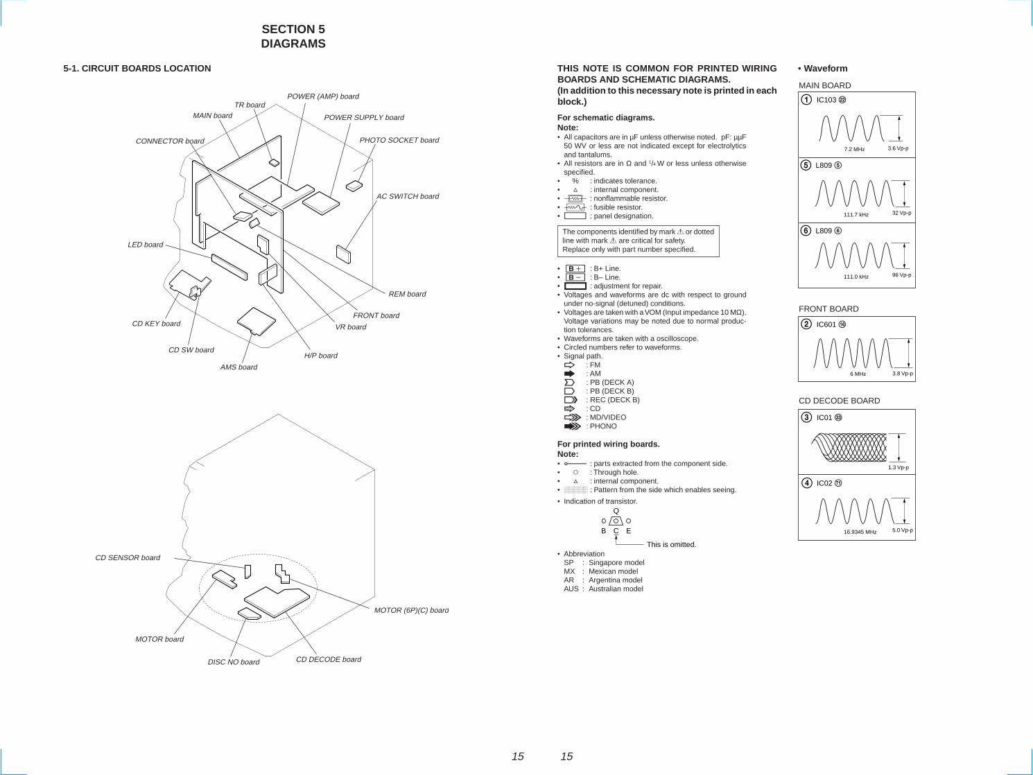
HCD-DR3/DR330/XB200
1616
5-2. BLOCK DIAGRAMMAIN SECTION
: FM
: CD
• Signal Path
• RCH is omitted • Abbreviation SP:Singapore AR:Argentina
CCD
SECTION
TU L
ST IND
TU MUTE
DO1
Q709
MUTE
14 7
4
POWER AMPIC701
SPEAKERRELAYDRIVE
Q711
1
2
6
IC702
RL701
SPEAKER
PHONES
JK703
JK701
SCOR
SENS1
SQSO
XLAT
SQCK
CLK
CE
STB
91
STB
100
SCLK
98
SDAT
A OU
T
95
DATA
97
SQCK
94
XLAT
96
SQSO
11
SENS
1
27
SCOR
99
SDAT
A IN
9
MD
MUT
E
73
FM S
T IN
D
2
SYST
EM M
UTE
1
POW
ER O
UT
LED DRIVEIC603
1
2
3
88
LATC
H
DI
CLK
RESETSWITCH
POWERDOWN DET
Q601
Q602
LED610-615
X2
17
X1
16
VR U
P
81
X6016MHz
VR D
OWN
82
VR601VOLUME
CD D
OOR
79
A B
S653DOOR SW
2
3
RM601
REMOTECONTROLRECEIVER
KEYMATRIX
S601-651
K0 K4
FLD601
SYSTEM CONTROLLER/FLD DRIVER
IC601
-5.6VREG
Q308
SITCHING
Q309
+7.5VREG
Q702
CD +7.5V
+12VREG
Q701
RECT
D701
AC OFFDET
Q704 705
RECT
D705-708
220-240V
110-120V
-27VREG
Q703
IC701 B+
AC IN
AC IN
T001
S001AC5.4V
AC5.4V
16
ATUNER
SECTION(PAGE 17)
(PAGE 17)
(PAGE 17)
: PB (DECK A)
: PB (DECK B)
: REC (DECK B)
CLK DI
87
LOCK
BUS REGISTERIC607
REC MUTE13
PLAY MUTE14
A/B11
BIAS12
SI2
CLK3
STB1
DI
CLK
4PLAY
5SOL A
6SOL B
SOL ADRIVE
Q612,615
M+12VSWITCH
Q610,613M+12V
SOL BDRIVE
Q611,614
SHIFT REGISTERIC606
CK2
S/L1
QH9
CLK3REC A
5PHOTO A
11A MODE SW
13A HALF
6PHOTO B
12B MODE SW
14B HALF
MECHABLOCK
D715
-5.6V
45 3019 23
Q'S10
SCOR
DATA IN
DATA
SENS2
LOCK
75
SENS
2
74
AMS
86
S/L
80
DATA
IN
HP901PB
HEAD
TAPE A
HRP901REC/PBHEAD
TAPE B
R CHR CH
R CH
PLAY/RECCONTROL
Q803,805
PLAY/RECCONTROL
DRIVE
Q823
PLAY/RECCONTROL
D802
L609BIAS OSC
BIASOSC
HE901ERASEHEAD
5
7
6PB OUT
A/B
2
3
EQ AMPIC801
Q816,817
D803
Q801
BIASSWITCH
Q829,830
Q807
PHONO
JK201
R
LIC202
R CH
BIASTRAP
L805
SFR807
9
SFR807
SFR801
SFR803
14
10
13
11
12
8 1
SW
VALC
REC AMP
PB/REC AMPIC802
Q811
BUFFER
D807Q813
MUTECONT
Q825,826
16
14
DOLBY AMPIC803
12
9
11
5
D808
SFR805
Q822
PBMUTE
Q815
MUTE
D811
MD/VIDEOIN R
L
R CH
BIAS+12V
+12V
Q833
Q809
RECMUTE
Q831
AMS
Q832
TAPE PLAY7
D804
BCD
SECTION
IC303
MD/
VIDE
O
MD
(HI)
Q209
MUTE
8
6
10
12
9
11
IC203
Q210Q207
Q201
AMP
Q204
MUTEL1 (CD)2
L4 (AUX)9
L3 (TAPE)8
L2 (TUNER)7
L (REC)3
13 14
11VR
DATA CLK
SELECTORIC201
DATA
4
SURR
OUND
OUT
6
DBFB
ON/
OFF
5
DBFB
H/L
Q306
SURROUNDCONTROL
Q305
Q301
Q303
IC301IC302
MUTE
Q707
R CH
+12V
Q708
MD/VIDEO OUT
R
L
R CH
JK201
LED DRIVEIC602
2
45
LEDDRIVE
DI
CLK
Q608,609
LED605-608
LED516
6
11
14
16.
17.
7
9
11
14
.4
3
16DOLBY OUT
LED601-603
7 8 85
4REC B
12
13
4
5
8
6
10
12
1
3
9
11
26
VACS
10
SPEA
NA H
/L
25
SPEA
NA 2
24
SPEA
NA 1
IC604
Q607
CLK
DI
100
SCLK
CLK
93
CECE
CD E
NCOD
ER A
83
CD E
NCOD
ER B
84
VR602CD ENCODER
A B
RESE
T
12
POW
ER D
OWN
13
REM
OTE
29
VCCVCC
47 50 52 68.P1 P21 G1 G16
FLUORESCENTINDICATOR TUBE
MUTESWITCH
Q713
+12V
IC701 B-
-30V
+5.6VREG
Q310
+12V(CASSETTE)
D+12V(MOTOR)
+12V(BIAS)
D601
D602VCC
+12V(TUNER)
+5.6V
µCON B+
CD L
Q205
: MD
FOK
CNIN
76
FOK
28
CNIN
UP S
W
77
TABL
E SE
NSOR
78
S06UP SW
TABLESENSOR
SENS01
F702
F703
F702
EXCEPT E,SP,AR
E,SP,AR MODEL
AC VOLTAGE
HCD-DR3/DR330/XB200
1717
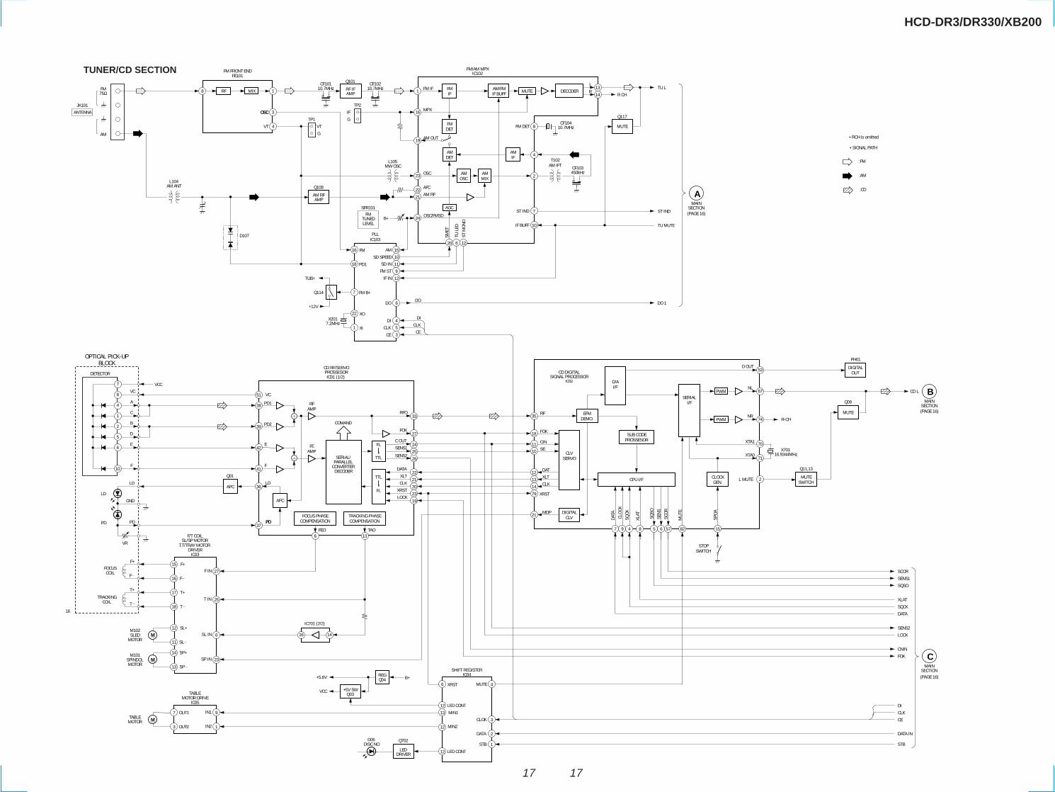
TUNER/CD SECTION
CE
16
10
6
5
3
22
1
PLLIC103
FM
XO
XI CLK
DO
CE
CLK
DO
OPTICAL PICK-UPBLOCK
APC
Q0141
VCCVC
LD
GND
A
C
B
E
F
FOCUSCOIL
F+
F
T+
TTRACKING
COIL
36
37
42
39
38
51
APC
FOCUS PHASECOMPENSATION
DECODER
SERIAL/PARALLEL
CONVERTER
FEAMP
RFAMP
IIL
TTL
TTL
IIL
COMAND
VC
TRACKING PHASECOMPENSATION
LD
PD
E
F
PD1
PD2
6
25
24
21
20
23
22
33
27
SENS1
RFO
FOK
C OUT
DATA
XLT
CLK
XRST
13FEO TAO
IC03
T.T/TRAY MOTORDRIVER
CD RF/SERVOPROSSESORIC01 (1/2)
15
25T IN
16
17
18
VR
PDPD
12
11
14
13
27F IN
6SL IN
9IN1
F+
F
T+
T
SL+
SL
SP+
SP
M
M
MOTOR
M102SLED
MOTOR
M101SPINDOL
EFMDEMO.
XRST
CLVSERVO
DIGITALCLV
D/AI/F
SUB CODEPROSSESOR
CPU I/F
7 9 4 5 6 6257
MDP
SENS
SCOR
SQSO
SQCK
CLOC
K
DATA
CLK
XLT
DAT
SE
CIN
FOK
RF
SERIALI/F
PWM 67
70
71
NL
XTA1
XTA0X701
MUT
E
R-CH
CD DIGITALSIGNAL PROCESSOR
IC02
16
:FM
:CD
• SIGNAL PATH
14
7
8
4
2
1
6
10
DETECTOR
16
OSC
FM75Ω
AM
ANTENNA
JK1013
8 RF MIX 1
4
FM FRONT ENDFE101
RF IFAMP
Q101CF10110.7MHz
CF10210.7MHz
L105MW OSC
IF
G
VT
L104AM ANT
AM RFAMP
Q108
MPX16
FM IF1
OSC23
AFC22AM RF21
FMIF
AM OUT19
FMDET
AM/FMIF BUFF
AMOSC
AMMIX
AMDET
SMET
20
CF103450kHz
MUTE
AGC
AMIF
DECODER13
L
14R
4
2
T102AM IFT
8FM DETCF104
10.7MHz
R CH
FM/AM MPXIC102
FMTUNEDLEVEL
PD118
X2017.2MHz
FM B+7
TUB+
+12V
Q114
ST M
ONO
12
15AM
OSC/FMSD24B+
11SD IN
9FM ST
TU L
ED
6
12IF IN
SD SPEED
7ST IND
10IF BUFF
MUTE
Q117
TU L
ST IND
TU MUTE
DO 1
AMAIN
SECTION(PAGE 16)
D5
LD
PD
F/T COILSL/SP MOTOR
7
3
OUT1
OUT2MMOTOR
TABLE
23SP IN
1IN2
IC701 (2/2)
XRST6
Q702
12 LED CONT
13
12
MIN1
MIN2
4MUTE
3CLOK
1STB
IC04SHIFT REGISTER
35
18
11
10
12
13
14
79
21
15
SPOA
STOPSWITCH
8
XLAT
CLOCKGEN.
PWM 74NR
MUTE
Q09
CD L
SCOR
SENS1
SQSO
XLAT
SQCK
DATA
CE
STB
CLK
CMAIN
SECTION
:AM
• RCH is omitted
SFR101
CNIN
FOK
OSC
VT
G
TP2
TP1
2DATA
26SENS2
19LOCK
16.9344MHz
2L MUTE
53D OUT DIGITAL
OUT
PH01
BMAIN
SECTION
DATA IN
D107
4DIDI
DIIC05
TABLEMOTOR DRIVE
12 LED CONT
DRIVERLED
DISC NOD06
Q04REG
Q03+5V SW
B++5.6V
VCC
SENS2
LOCK
MUTESWITCH
Q11,13
(PAGE 16)
(PAGE 16)

HCD-DR3/DR330/XB200
1818
5-3. PRINTED WIRING BOARD MAIN SECTION • Refer to page 15 for Circuit Boards Location.
Ref. No. Location
• Semiconductor LocationRef. No. Location
D07 J-11D08 J-10D09 J-9D10 J-8D101 C-2D102 C-2D103 A-2D104 A-2D107 B-3D109 C-5D110 B-8D111 A-8D301 E-4D302 D-10D303 I-4D304 B-11D305 D-3D306 E-7D307 A-9D308 A-9D309 C-11D310 C-11D802 I-9D803 I-9D804 F-8D805 C-11D806 D-11D807 E-7D808 E-7D811 I-10D812 F-12
IC102 B-6IC103 D-3IC201 E-4IC202 H-3IC203 F-3IC301 F-4IC302 H-4IC303 B-9IC801 G-8IC802 F-8IC803 G-6
Q101 B-5Q108 A-3Q114 C-3
Q116 B-7Q117 A-7Q201 D-9Q202 E-7Q203 C-9Q204 D-8Q205 C-10Q206 H-8Q207 E-3Q208 E-3Q209 E-3Q210 D-3Q301 H-4Q302 G-5Q303 H-4Q304 G-5Q305 G-4Q306 D-10Q308 I-4Q309 I-4Q310 A-10Q801 F-10Q802 G-9Q803 G-10Q804 G-10Q805 G-10Q806 G-10Q807 F-8Q808 G-7Q809 H-9Q810 F-6Q811 G-7Q812 F-6Q813 H-7Q814 F-6Q815 H-6Q816 I-10Q817 I-10Q822 E-6Q825 G-10Q826 F-10Q829 E-11Q830 E-11Q831 D-11Q832 D-11Q833 F-12
MAIN BOARD
LED BOARD
JK101ANTENNA
AM
FM
R L
R L
R L
IN
MD/VIDEO
PHONO IN
OUT
16
JK201
TO AMP BOARD
CN701(Page 22)
CTO
CD DECODERBOARDCN03
(Page 24)
D
TOFRONT BOARD
CN601(Page 26)
B
TOFRONT BOARD
CN602(Page 26)
A
1-674-636-
11
(11)
(4144268510)
1-674-637-(CASSETTE BOX BACK LIGHT)
11
(11)
(4144268520)
12
1
1
1
1
1
3
1
13
8
916
1 8
916
5
2
2
2
21
1 4
58
1
1
1
1
1
1
14
15
11
12 22
458
12
1324
28
7
8 14
4
58
1
1
1 8
916
12
1
1
3
6
4
58
5 8
14
HRP901RECORD/
PLAYBACKHEAD
HP901PLAYBACK
HEAD
HE901ERASEHEAD
X
B DECK
A DECK1
2
1
1
1
16
1
16
2345
2
3
D104
L104
L105L109
L108L114
D103
D107C114
C179
C187
C113
C116
C115
C188
C189
C129
C154
C121
C126
C127
C122
C161
C198C140
C142
C141
C160 C257
C132
C139
C256
C11
7
C16
3
C12
0
C12
8
C13
8
C13
7
C16
4
C13
1
C13
0
C12
5 C13
3
C33
3 C34
3
C33
9D
309
D80
5
D31
0
C35
0
C14
9
C12
4
C12
3
C15
1
C13
5
C17
7
C15
9C
194
C19
5
C19
9
Q21
0
Q20
8
Q20
7
R26
8
Q82
2
Q81
2
Q81
4
Q81
1
Q20
2
Q30
6
C15
2
C32
7
C21
9
C22
3R
267
C31
2C
346
C30
1
R31
8
R322
C320
C302
R32
4R
311
R31
4
R30
3
R30
7R
320
C30
5
C31
6R
305
C314
R31
6
C309 C307R301
IC30
1C222 C311
C220
C214C213
C250
C24
4
C24
0C
239
C23
2
C23
6
C85
8
C86
4
C857
C860
C862 C866
C23
0
C22
8
C23
4
C32
8
C87
6
D80
8
D80
7
C24
6
D30
5
C15
5
C14
8
C14
3
L113
C10
8
C14
4
C15
0
C16
5C
185
R15
5
R10
4
R11
2
R13
7R
136
R11
6
R11
5
R14
0
R13
5R
260
R22
9
R25
4
R25
5
R35
2
R30
2
C30
2C
310
R30
6
R24
3
R24
5C
243
C30
8C
306R35
4
R25
6
R25
3
R22
8
R35
5
R89
1R
887
R85
4
R87
0
R86
8
R83
1
R83
8
R84
7R
844
R23
7
R23
9
R23
3
R24
9
R23
5
R82
8
R82
5
R81
9
R84
1 R83
9
Q80
1
Q805 Q803
Q806
Q80
2
Q804
R804
R893
R802
R82
7
R80
5R
806
R90
1
R89
6R
899
R80
8
R89
5
R80
7R
897
R80
9
R81
1R81
0
R80
0AR
820
R52
7R86
7
R88
3R87
3
R88
2
R87
8R
877
R87
5
R86
3
R86
1
R32
6
R33
2
R31
2
R86
4 R86
2R
866
R87
4
R82
4
R85
5R
881
R81
8
Q81
6
Q82
3
Q80
9
Q20
6
Q81
3Q81
5
Q81
7
R89
4
D81
1
D80
2D
803
CN
802
CN
811
CN
812
R81
7R
905
R82
1SF
R80
3
SFR806
SFR804
SF
R80
5
SFR801
SFR807
SFR802
SFR808
IC801
C82
9
C819
C815
C811
C825
C820
C806
C803
C82
1 C89
6
C83
7
C835
C84
5
C80
7
C81
3
C82
2 C80
1C
802
CN
803
C88
6
C88
1
C87
7
C88
7C80
5C81
8
C82
4
C85
3C
865
C86
9C86
1
C89
3
C90
7
C33
7
C33
4C
315
C31
3
C24
9
C32
1
C31
9C31
8
C323
C32
2
C20
5
C21
8
C21
7
IC30
2
IC20
2
C24
8C20
1
C20
4
C33
8
C335 C336
D303
C32
4C
325
CN
801
CN
302
C81
6
C814
C80
9
C90
2
C87
5
C882
C82
3
R83
7
R89
2
R23
6
R88
8
R85
8R
845
R85
3R
846
R82
5
R25
0
R33
0
R11
7
R13
3R
134
R71
4
R13
9
R13
2
Q10
8
TC102G DS
R114R113
R118
R119
C14
6
R106 R167
R144
R151R118
R123
R121
R17
5
R15
7
R34
4
R14
1R
142
R24
1
R23
1
R24
0
R92
6
R84
3
R35
3
L806
C92
2C
884
C83
9C
849
C83
8
C84
8
C83
3
C34
5C
227
C23
1
C23
3
C82
8
C84
7
C90
6
C23
7
Q20
5
Q83
2
R24
2
R14
3
R33
9
R33
7
R88
9
R17
2
R13
0
D11
0R
131
R12
7R
129
R12
0
R17
3
SF
R10
1
R18
0
R147R107
R105D109L106
FE101
C157
C156
C162
C158
CF101
CF
102
CF
103
CF
104
Q101
Q114
T102
R124
Q117
Q116
B
B
E
E
B E
R156
R128
R126IC102
IC103
IC201
TP1
X101
D102D101C186
S
S
GD
D
C196
C260
C226C242
C235
C197
G
C221B
BE
E B
B
B
B
B
B
E
EE
E
E
E
B
E
B
E
D301
R259
R265
R266
R264
R263
R258
R334
R234
R238
R848R849
R842
R830 R829
R232
Q204
R836C867C825
C894Q810
D306
D111D307
D304
D308
IC303
C347
C330C341
C340R338
R138
R346
R345
L301
L302C342
Q310B
E
CN602
CN601
R925
R924
R917
R916
R918
R919
R921
R920
R92
3
R92
2
C905
C925
D302
S
D
G
C903
C90
4
B
B
E
EQ831
D806
Q833
Q830
Q829
BB
B
E
E
E
R912
R913
R911
R931
R930R906
D812
CN
809
C841
C842
R833
R835
R815
R814R832
R840R834
C883
C846
C840
IC802
C834
C827C836L804
C856
R329
R333
Q203
Q201
B
BE
E
C238 C329
C229L803
GDS
Q807B
EL801
C817
C826C831
C851
D80
4
R823
R803
R907
Q82
5B
B
B B
B
B
B
B
B
B E
E
E
E
E
E
E
E
B
B
E
E
E
E
Q82
6B
ER801
L805
R890
C885
L809
C888
L808C921
R898
C880
E
E
E
BB
B
CN808
C897
C808
C901
C812C804
R812
R816 R822Q808
R251
R252
R225
R227
Q209
IC203R310
R262R261
R309
R244
R308
C24
7R351
C241
R304C304
R850
C830
C832C895
C855
C800A
C854R856
R872 R860
R884
R85
9C870
L802
R826
GN
D30
2
GN
D30
1
CN302D10 D09 D08 D07
R448
R851
C891R328
C863C868
C908
C859
R871
R857
R915
R865
IC803
R869
CN401
CN301
CN807
R914
R880
R876
C892
C216
R208 C210
C212
R214
R21
9
R31
3
R31
5
R32
3
R33
1
R21
2
R20
6
C20
6
R20
4R
202 R
201
R21
3R
215
R21
6
R21
8
R22
2R
223
R20
5R
221
R22
4C
202
C20
7C
209
C20
8C
252
R220R210
C255R350
R347
R247R245
R327B
BE
E
Q30
8Q
309
R357R321
R317C317
R246
R325
R24
8
Q30
2
Q30
3
BE
BE
R31
9
C215
C211R211R209
C251R356
Q305
Q30
1
R217
G S D
C203
R207
R203
BE
BE
Q304
21
XB200MODEL
XB200MODEL
XB200MODEL
C107
DR3/DR330MODEL
1 2
A
B
C
D
E
F
G
H
I
J
3 4 5 6 7 8 9 10 11 12

HCD-DR3/DR330/XB200
1919
5-4. SCHEMATIC DIAGRAM MAIN (1/3) SECTION • Refer to page 15 for Waveform. • Refer to page 31 for IC Block Diagrams.

HCD-DR3/DR330/XB200
2020
5-5. SCHEMATIC DIAGRAM MAIN (2/3) SECTION • Refer to page 15 for Waveform. • Refer to page 18 for Printed Wiring Board.

HCD-DR3/DR330/XB200
2121
5-6. SCHEMATIC DIAGRAM MAIN (3/3) SECTION • Refer to page 18 for Printed Wiring Board. • Refer to page 31 for IC Block Diagrams.

HCD-DR3/DR330/XB200
2222
5-7. PRINTED WIRING BOARD AMP SECTION • Refer to page 15 for Circuit Boards Location.
Ref. No. Location
D701 H-3D702 E-7D703 I-6D704 E-7D705 H-1D706 H-2D707 H-1D708 H-2D709 H-1D710 G-4D712 G-7D713 F-7D714 F-2D715 G-7D716 G-3D717 F-2D718 H-6D719 G-2
IC701 E-3IC702 G-7
Q701 C-6Q702 D-7Q703 I-7Q704 G-2Q705 G-2Q706 E-2Q707 E-2Q708 G-7Q709 F-3Q710 F-6Q711 G-6Q712 G-7Q713 G-5
• SemiconductorLocation
R729R728
CTO MAIN BOARD
CN401(Page 18)
POWER AMP BOARD
H/P BOARD
TR BOARD
POWER SUPPLY BOARD
AC SWITCH BOARD
R
JK703SPEAKER
AC IN
L
GND
AC4
AC3
AC5
P1
P2
P3
P4
P5
AC6
AC5.4V
AC5.4V
T001POWER
TRANSFORMER
1-674-640-
11
(11)
(4146269610)
1-674-638-
11
(11)
(4144268530)
1-674-880-
11
(11)
(4144268540)
1-674-641-1-674-642-
11
(11)11
(11)
(4146269620)
AC1BLU
AC2BRN
P6 P7
P2
P8
P4P3
P1 F70
2
F703
GND2
POWER SUPPLY BOARD
AC IN
GND
AC4
AC3
AC5P6
P7
AC6
AC5.4V
AC5.4V
T001POWER
TRANSFORMER
1-674-638-
11
(11)
(4144268530)
AC1BLU
AC2BRN
P6RED
P7WHT
P2
P5
P8
P4P3
P1 F70
2
R00
1
GND2
B E
B E
15
CN704
Q701
JK701PHONES
1
1
5
7
1
1
12
8
A
R735
R737R738
L703
R736 R705 R711
R742
R714
R720
R704
R719
R707 R709
C703 C713 C710C702
C740C753
C758C755
C752
C754
C75
6
C75
7
D71
3
C738
C739
C724
C76
4
C718
C717Q711
C727C728
C726
Q702CN704
C719C708
R703
R763
R73
9R
764
R76
6
R76
5
R72
4
R70
1
R72
5
R710
R75
1
R70
8
C71
4
C70
9 C70
4R
706
Q71
0
IC70
2D
712
D71
0
CN
701
Q71
2
R72
6Q
709
R76
2R
L701
R723IC701
C701
C759
C705
C707C711
C706
C72
1
C72
2L7
02
CN702
CN702
Q707
Q706
D714
D717
D719C762
BE
B
B
E
E
E
E
B
B
EB
R744
R733
R730
R716
R712
R750
R760
R743
R731C725
R73
2
R71
5
R76
1
R74
0
C74
3
D70
1
D70
9
D70
5
Q70
5
Q70
4
R74
9
R74
8
C73
3
R74
7
D70
7
D70
8
D70
9
D71
6
GN
D
GN
DA
C3
AC
4A
5.4V
A5.
4VA
C5
AC
6
C74
5
C74
4
C74
6
C74
8
C76
3
C74
9C
747
C75
0
R75
3R
754
Q71
3R
752
R72
7R
734
R72
2R
721
R71
3
D704D702
R702
Q708
C723
E
B
E
BD715
D718
D703
C736
C734
C735
C737
C742
C741C751
Q703
GN
D
S
D
G
CN703F701
Z
Z
S
D
G
15 2 1
16
DR3/DR330MODEL
DR3DR330MODEL
XB200MODEL
VOLTAGESELECTOR
220-230V 120V
P5
NOT REPLACEABLE:BUILT IN TRANSFORMER
EXCEPT E,SP,AR
E,SP,AR MODEL
1 2
A
B
C
D
E
F
G
H
I
J
3 4 5 6 7 8 9 10 11 12 13

HCD-DR3/DR330/XB200
2323
5-8. SCHEMATIC DIAGRAM AMP SECTION • Refer to page 32 for IC Block Diagram.
AUS, XB200:T2.5AL 250VMX:5A 250V
EXCEPT E,SP,AR MODELS
E,SP,AR MODELS
JK703
The components identified by mark ! or dottedline with mark ! are critical for safety.Replace only with part number specified.

HCD-DR3/DR330/XB200
2424
5-9. PRINTED WIRING BOARD CD DECORD SECTION • Refer to page 15 for Circuit Boards Location.
DTO MAIN BOARD
CN301(Page 18)
ETO FRONT BOARD
CN11 (Page 26)
11
(11)
(4146266810)
11
(11)
(4146266820)
11
(11)
(4146266830)
11
(11)
(4146266860)
11
(11)
(4146266840)
11
(11)
(4146266850)
MOTOR
M102SLED
CN03
6
1
M101SPINDLEMOTOR
M_+
_
S05LIMIT
+
_M_
MOTOR (6P) (C) BOARD
MOTOR BOARDCD SENSOR BOARD
DISC NO BOARD
PHOTO SOCKET BOARD
CONNECTOR BOARD
1-639-678-11
M_
(TABLE MOTOR)
1 4 1 3
1
1 2
3
12
34
5
CD DECODER BOARD
1
1
1
111
1
16
1
4 6 3
2
9
7
BB
E
E
9
2
16
15
B
B
E
E
B
B
B
B
E
E
E
B
B
B
E
E
E
E1
3
R47
SENSO1
CN05
C43S06
CN08MO1
PH01CD DIGITAL OUTOUT(OPTICAL)
D06
CN06
(DISC NO LED)
OPTICAL PICK-UPBLOCK
KSM-213ECM/C2NP
1 221
16
1 2
A
B
C
D
E
F
G
H
I
3 4 5 6 7 8 9 10 11 12
Ref. No. Location
D02 D-3D05 E-6D06 D-11
IC01 C-3IC02 C-6IC03 D-4IC04 B-7IC05 F-5
Q01 C-2Q02 B-2Q03 E-5Q04 E-6Q06 D-4Q07 C-7Q09 D-7Q10 C-7Q11 D-7Q12 C-8Q13 D-8Q14 C-7
• SemiconductorLocation

HCD-DR3/DR330/XB200
2525
5-10. SCHEMATIC DIAGRAM CD DECORD SECTION • Refer to page 15 for Waveforms.
M
The components identified by mark ! or dottedline with mark ! are critical for safety.Replace only with part number specified.

HCD-DR3/DR330/XB200
2626
5-11. PRINTED WIRING BOARD FRONT SECTION • Refer to page 15 for Circuit Boards Location.
Ref. No. Location
D601 C-11D602 C-11D603 D-10D604 D-12D605 C-11D606 B-9D608 B-8D609 B-8D612 B-9D613 E-6D614 B-9D615 A-10D616 B-10D617 B-11D618 A-12D619 A-12D620 B-12D621 F-4D622 E-5D624 E-6D723 B-9D730 A-10D731 B-9
LED601 A-5LED602 A-3LED603 F-10LED605 E-8LED606 E-9LED607 E-10LED608 E-11LED610 I-3LED611 I-4LED612 H-4LED613 H-3LED614 H-12LED615 H-12LED616 I-5
IC601 D-8IC602 F-8IC603 G-3IC604 B-11IC606 E-4IC607 E-6
Q601 D-11Q602 D-12Q603 E-10Q604 E-10Q607 B-10Q608 G-4Q609 G-4Q610 F-7Q611 F-5Q612 F-6Q613 F-6Q614 E-6Q615 F-6
• SemiconductorLocation
(4146268910)
TO CONNECTOR BOARD
CN11(Page 24)
B
E
TO MAIN BOARD
CN601(Page 18)
1-674-630-
(4146268950)
1-674-634-
11
(11)11
(11)(4146268930)1-674-632- 11
(11)(4146268960)
1-674-635-
11
(11)
(4146268940)1-674-633-
(416268920)1-674-631-
11
(11)
11
(11)
FRONT BOARD
AMS BOARD CD KEY BOARD
CD SW BOARD
REM BOARD
VR BOARD
R687R688
C631
C634
D621
18
10
1
9
16 11
112
2
33
1
1
1
1
11 10 2820 30
30
31
36 40 50
50
51
51
54552 3
16
89
1
8 9
16
16
3
15
162
3
1100
80
81
19
10 18
17
8 14
16
1
16
1
16
1
1
3
3
TO TAPEMECHANISM
ATO
MAIN BOARDCN602
(Page 18)
S653
CN608
VR602AMS
R66
6
R66
7
R66
3R
662
R66
8
R66
5
LED616
R664
S647DISC SKIP
S644EDIT
S639DISC 1
S640DISC 2
S641DISC 3
S642DISC 4
S636DOLBY NR
S635DIRECTION
S643DISC 5
S650PLAY MODE
S622FUNCTION
S612TUNING +
S613TUNING –
VR601VOLUME
S631ENTER/NEXT
S619STEREO/MONO
S633TUNING MODE
S625DAILY
S626REC
SP
EC
TR
UM
AN
ALY
ZE
R
S624
S627SLEEP
S614ROCK
S615POPS
S616JAZZ
S618FLAT
S620DBFB
S634GROOVE
S621SURROUND
S617SALSA
DISPLAY/DEMO
S632TUNER/BAND
S630TUNER MEMORY
S651REPEAT
S638CD SYNCHRO
S648
S649
S645
S646
S637
CN603
CN603
R65
8R
659
R65
1R
652
R66
0R
661
CN608
CN606CN606
R620
R61
9
R65
4
R62
3R
692
R621
R653
R622
S603S605S604
S601 S602
LED615 LED614
A DECKB DECK
REC
C667
S611
R756
R62
8
R62
7
R62
4R
689
R68
2
R73
3R
726
R73
4R
684R
702
R74
9 R73
7 R73
8
R73
9R
746
R75
7R
773
R72
5
R75
6R
748
D62
2
C67
3
C66
1
C62
4
C66
5
D61
3
IC
607
IC
606
D62
4
R77
1
R76
1
R74
7
R67
6
R75
0
R74
1R
770
R73
0
R69
1
R61
0
IC60
3
R69
0
Q60
9
R751R752
LED611LED610
LED613 LED612
S606
S609 S608S610
S607R625
R763
R762R685
R626
S
D
G
Q60
8
S
D
G
C633
C629C630
C632
16
SFR601
R736
R727
R683
CN607
CN605
E
E EB
B B B
B
B
E
EE
Q61
1
Q61
4
Q61
2
Q61
5 Q61
0
Q61
3
C664
R635
R678
R606
R735R772
C662C623
C660
C663R745R681
C659C658R732R731R729R728
CN605
CN
604
RV601
RM601
C666
LED602
LED601
R646
R647
R62
9
C62
1
C67
2
D60
9D
608
D61
2
D72
3
D73
0
D61
8D
619
D73
1D
614
D61
6
D60
3
C64
4
C65
0 C64
9
C64
5
C65
1
C64
0
C66
9
R67
5
R76
0
R70
9
R70
6
R70
7
R63
9R
605
R61
3
R61
4
R60
2
R60
4
C60
4
R61
5
R64
2
R76
4
R70
5
R64
5
R63
0
R70
4
Q60
7
Q60
2
LED
608
LED
606
LED607LED605
LED603
CN
602
CN
601
R71
7
R71
8
R71
0
R71
4
R71
1
R71
5
C64
3
C64
8
D60
6D
607
R64
8
R64
9
R693R694
R615
R611
R612
RA603 RA605 RA604RA602RA601
C627 C628
FLD601
R618
R758
R617
D615
D61
7
D620
R713
C647C653
IC604B
BB
E
E
E
R719
R723
R724
R722R721
C646
C655
C670C668
C654
S623
R640
R641
R603
C671
/CLOCK SET
D602
D605
D604
D601
R679
C622
C620
C619
C612
C626
S629S628
R643
R644
CN11
CN604
R695
R631
R70
1
R63
4
R63
3
C60
9 C61
8
C60
2
C61
6X60
1
C63
5
C63
9R
700
R70
3
R69
7R
698
R69
9
R60
8
Q60
4
Q60
3
R60
7
E E
BB
C601
TP601
R636
R632
R606
R637
IC602
C636
C637
C638
C613
C614
C610C611
C625
C606
C608C603C607
C605
IC601
L601
Q601
R601R616
(DOOR SW)
EXCEPT E,SP
Q60
6
Q60
5
B
E
B
E
D61
1
DR3:AUSXB200MODEL
DR3:MXDR330 MODEL
DR3:MX,AUSDR330/XB200MODEL
DR3:E,AUSXB200 MODEL
DR3:SPMODEL
1 2
A
B
C
D
E
F
G
H
I
J
3 4 5 6 7 8 9 10 11 12 13

HCD-DR3/DR330/XB200
2727
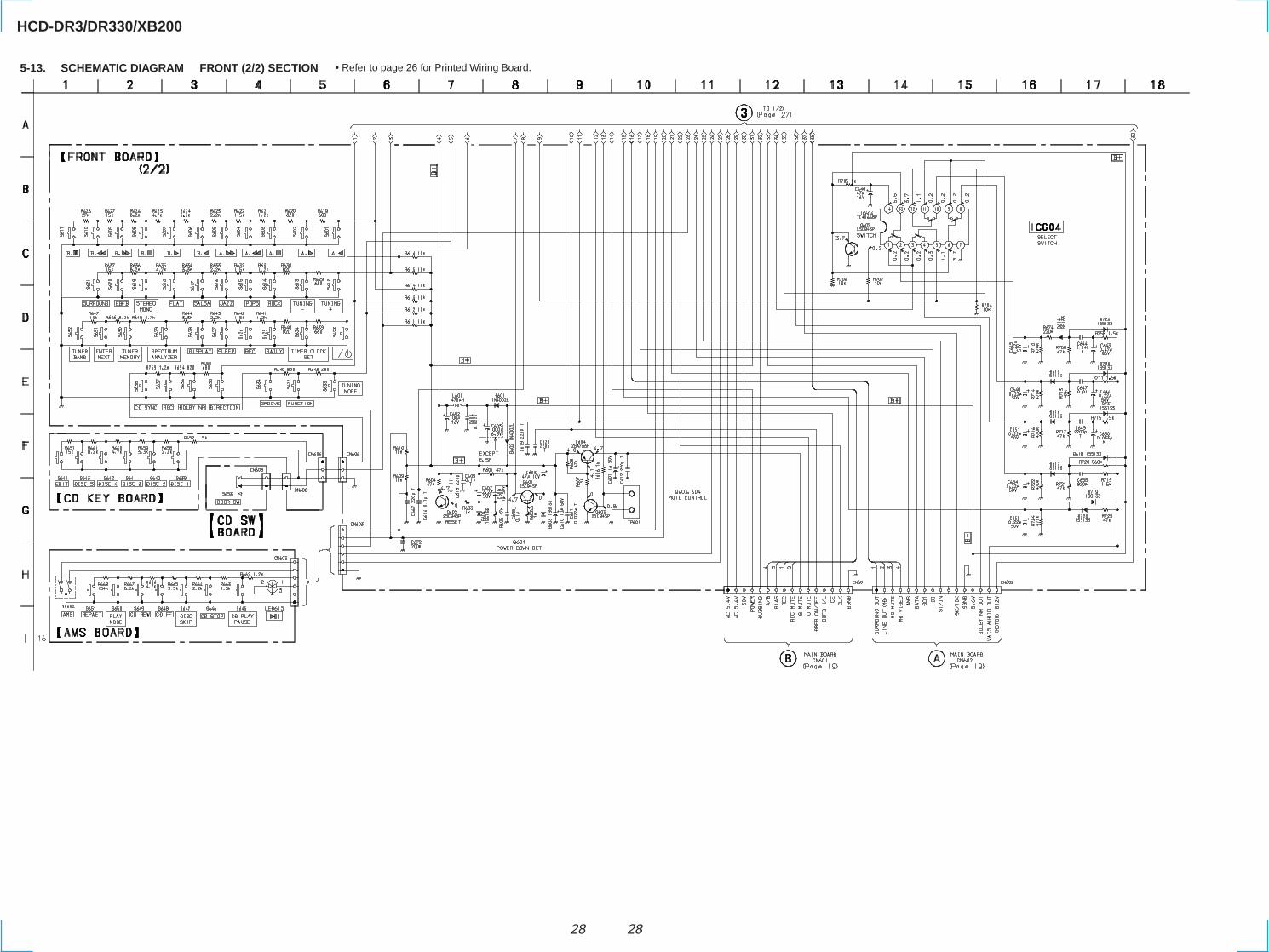
5-12. SCHEMATIC DIAGRAM FRONT (1/2) SECTION • Refer to page 15 for Waveform. • Refer to page 29 for IC Pin Function Description. • Refer to page 32 for IC Block Diagrams.
HCD-DR3/DR330/XB200
2828
5-13. SCHEMATIC DIAGRAM FRONT (2/2) SECTION • Refer to page 26 for Printed Wiring Board.

29
5-14. IC PIN FUNCTION DESCRIPTIONIC601 LC866540A-5K40 SYSTEM CONTROL (FRONT board)
Pin No.
1
2
3
4
5
6
7
8
9
10
11
12
13
14
15
16
17
18
19
20
21
22
23
24
25
26
27
28
29
30
31
32
33
34
35
36
37
38
39
40
41
42
43
44
45
46
47
48
49
50
I/O
O
O
O
O
O
O
O
O
O
O
I
I
I
—
—
—
—
—
I
I
I
I
I
I
I
I
I
I
I
O
O
O
O
O
O
O
O
O
O
O
O
O
O
O
O
—
O
O
O
O
Description
Power on/off output
System mute output (ON at H)
Tuner mute output (ON at H)
Surround output (ON at H)
DBFB normal output (ON at H)
DBFB high output (ON at H)
MD/VIDEO output
MD(HI) output
Function mute(Line out mute)
Spectrum analyzer 1,2/3,4
CXD2589Q SCOR input
Reset
Power down in(AC on at H,AC off at H)
FLD VDD
Ground
X’tal oscillator 6MHz
X’tal oscillator 6MHz
System VDD 1
Key input 0
Key input 1
Key input 2
Key input 3
Key input 4
Spectrum analyzer 1
Spectrum analyzer 2
Vacs in
CXD2588Q SCOR input
CXD2588Q COUNT input
Remote in
FLD digital output 16
FLD digital output 15
FLD digital output 14
FLD digital output 13
FLD digital output 12
FLD digital output 11
FLD digital output 10
FLD digital output 9
FLD digital output 8
FLD digital output 7
FLD digital output 6
FLD digital output 5
FLD digital output 4
FLD digital output 3
FLD digital output 2
FLD digital output 1
FLD VDD
FLD segment output 1
FLD segment output 2
FLD segment output 3
FLD segment output 4
Pin Name
POWER OUT
S.MUT
TU.MUT OUT
SURROUND OUT
DBFB HI/LOW
DBFB ON/OFF
MD/VIDEO
MD(HI)
MD MUTE
SPEANA H/L
SENS 1
RESET
POWER DOWN IN
VDD
VSS
X1
X2
VDD1
K0
K1
K2
K3
K4
SPEANA IN 1
SPEANA IN 2
VACS IN
CXD2588Q SCOR
COUNT
REMOTE IN
16G
15G
14G
13G
12G
11G
10G
9G
8G
7G
6G
5G
4G
3G
2G
1G
VDD
P1 S0
P2 S1
P3 S2
P4 S3

30
Pin No.
51
52
53
54
55
56
57
58
59
60
61
68
69
70
71
72
73
74
75
76
77
78
79
80
81
82
83
84
85
86
87
88
89
90
91
92
93
94
95
96
97
98
99
100
I/O
O
O
O
O
O
O
O
O
O
O
I
I
I
I
I
—
I
I
I
I
I
I
I
I
I
I
I
I
O
O
O
O
—
—
O
O
O
O
O
O
O
O
I
O
Description
FLD segment output 4
FLD segment output 5
FLD segment output 6
FLD segment output 7
FLD segment output 8
FLD segment output 9
FLD segment output 10
FLD segment output 11
FLD segment output 12
FLD segment output 13
FLD segment output 14
FLD segment output 15-21
FLD segment output 22
FLD segment output 23
Destination selector switch input
VDD
FM stereo indicator input
AMS input
CXD 2589Q SENS input
CXD 2589Q FOK input
Changer mechanism UP switch input
Table sensor switch input
CD door switch input
HC 165 data in
VR encoder(+) input
VR encoder(-) input
CD encoder input A
CD encoder input B
M62433 S.DATA
HC165 S/L
CXA1992 LOCK output
BU2114 LATCH output
System Vss 2
System VDD 2
HC4094 STB output
CDP 2589 clock output
7218 standby output
CXD2589Q XLAT output
CXD2589Q DATA output
SQSO output
SQCK output
Serial data output
Serial data input
Clock output
Pin Name
P4 S3
P5 S4
P6 S5
P7 S6
P8 S7
P9 S8
P10 S9
P11 S10
P12 S11
P13 S12
P14 S13
P15-P21
P22
P23
MODE
VDD
FM ST IN
AMS IN
CXD 2589Q SENS2
FOK
UP SW
TABLE SENSOR
CD DOOR SW
DATA IN
VR+
VR-
CD ENCORDER IN A
CD ENCORDER IN B
S-DATA
S/L
CXA1992 LOCK
BU2114 LATCH
VSS2
VDD2
HC4094 STB
CDP 2589 CLOK
7218 STB
CXD2589Q XLAT
CXD2589Q DATA
SQSO
SQCK
DATA
DI
CLK

31
5-15. IC BLOCK DIAGRAMS
PHASEDETECTOR
CHARGE PUMP
SWALLOW COUNTER1/16, 1/17 4BITS
12BITSPROGRAMMABLE
DRIVER
UNIVERSALCOUNTER
REFERENCEDIVIDER
POWERON
RESET1/2
CCBINTERFACE
1 2 3 4 5 6 7 8 9
16 15 14 13 12 11
10
17181920XO
UT
VSS
AOUT
AIN
PD VDD
FMIN
AMIN
XIN
DOCLDICE
IFIN
IO1
BO4
BO3
BO2
BO1
IO2
UNLOCKDETECTOR
DATA SHIFT REGISTER LATCH
IC103 LC72131M
–+
2 3 6 74 5 81V+
–+
V–
IC203 MC14066BF
1IN/OUT
7VSS
6CONTROL IN
5CONTROL IN
4IN/OUT
3OUT/IN
2OUT/IN
8 IN/OUT
14 VDD
13 CONTROL IN
12 CONTROL IN
11 IN/OUT
10 OUT/IN
9 OUT/IN
IC202 M5218AL
MAIN BOARD

32
1 2 3 4 5 6 7 8 9
1016 15 14 13 12 11
CONTROLCIRCUIT
12 BITSHIFT
REGISTER
12 BITSTORAGEREGISTER
OUTPUTBUFFER
(OPEN DRAIN)
1718
VDD
OE Q11
Q10
Q9 Q8 Q7 Q6 Q5Q4Q3Q2Q1Q0LC
K
CLOC
K
DATAVSS
IC602 BU2092F-E2
3
6
9
12
15
18
2
5
8
11
14
17
1
4
7 10
13
16SHIFT
REGISTER
LATCH
ENABLE
SIN
CK
LATCH
SOUT
EN
RST
GND
GND
VDD
O1
O2
O3
O4
O5
O6
O7
O8
GND
IC603 BU2114F
1 2 3 4 5 6 7 8
91016 15 14 13 12 11
CK A B C DENABLE
P
QA QB QC QD ENABLET
RIPPLECARRYOUTPUT
CLEAR
GND
LOAD
VCC
IC606 SN74HC161
1 2 3 4 5 6 7 8
OVER LOAD DET
F/FOFFSET DET
LATCH/AUTORESET
VCC ONMUTE
AC OFFDET
VCC
IC702 MPC1237HA
FRONT BOARD
AMP BOARD
33
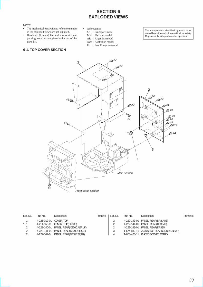
SECTION 6EXPLODED VIEWS
NOTE:• The mechanical parts with no reference number
in the exploded views are not supplied.• Hardware (# mark) list and accessories and
packing materials are given in the last of thisparts list.
The components identified by mark ! ordotted line with mark ! are critical for safety.Replace only with part number specified.
• AbbreviationSP : Singapore modelMX : Mexican modelAR : Argentina modelAUS : Australian modelEE : East European model
6-1. TOP COVER SECTION
Ref. No. Part No. Description Remarks Ref. No. Part No. Description Remarks
1
2
3
4
#2
#2
#2
#3#3
#3
#3
#4
#4#4#4
#4
Front panel section
Main section
#4
#1
#1
#1
1 4-221-012-01 COVER, TOP* 1 4-211-556-01 COVER, TOP(DR330)
2 4-222-140-01 PANEL, REAR(XB200:AEP,UK)2 4-222-141-01 PANEL, REAR(XB200:EE,CIS)2 4-222-142-01 PANEL, REAR(DR3:E,SP,AR)
2 4-222-143-01 PANEL, REAR(DR3:AUS)2 4-222-144-01 PANEL, REAR(DR3:MX)2 4-222-145-01 PANEL, REAR(DR330)3 1-674-880-11 AC SWITCH BOARD (DR3:E,SP,AR)4 1-675-425-11 PHOTO SOCKET BOARD

34
Ref. No. Part No. Description Remarks Ref. No. Part No. Description Remarks
6-2. CD DOOR SECTION
#6
#6
not supplied
#6
#7#5
#5
5153
5455
565760
61
6263
64
65
6667
68
5859
52
69
70
51 4-221-007-01 BUTTON, CD PLAY(DR3,XB200)51 4-222-126-01 BUTTON, CD PLAY(DR330)52 4-221-008-01 LENS, CD PLAY BUTTON53 4-221-006-01 BUTTON, CD SKIP(DR3,XB200)53 4-222-125-01 BUTTON, CD SKIP(DR330)
54 1-674-635-11 AMS BOARD55 4-221-011-01 SPRING (R), CD DOOR56 4-211-920-01 DAMPER (PG-5), GEAR57 1-674-632-11 CD SW BOARD58 4-221-128-01 LOCK
59 4-221-010-01 SPRING (L), CD DOOR60 1-674-634-11 CD KEY BOARD61 4-221-004-01 BUTTON, CD DISC(DR3,XB200)61 4-222-123-01 BUTTON, CD DISC(DR330)
62 4-221-005-01 BUTTON, CD EDIT(DR3,XB200)62 4-222-124-01 BUTTON, CD EDIT(DR330)63 4-220-995-01 PANEL, CD FRONT(DR3,XB200)63 4-222-120-01 PANEL, CD FRONT(DR330)64 4-221-002-01 RING, AMS
65 4-221-003-01 KNOB, AMS(DR3,XB200)65 4-222-122-01 KNOB, AMS(DR330)66 4-220-996-01 WINDOW, CD DOOR67 4-221-009-01 HOOK, CD DOOR68 4-221-001-01 DOOR, CD(DR3,XB200)
68 4-222-121-01 DOOR, CD(DR330)69 4-211-914-01 LENS, CD DOOR70 1-674-637-11 LED BOARD

35
Ref. No. Part No. Description Remarks Ref. No. Part No. Description Remarks
6-3. PANEL SECTION
#7
#7
#7
#7
#7#4
#7#7
#7
#7
notsupplied
Not supplied
Not supplied
101
102103
104
105106
107108
109
110111
112
113
114115
116117
118
119
120
121 122
123124
125 127128
129130
131
134
135 136
137
138139
140
141
132142
143
144
144145
142
126
133
146
126
101 4-221-028-01 BUTTON (R), CASS(DR3,XB200)101 4-222-130-01 BUTTON (R), CASS(DR330)102 4-221-034-01 LENS (A), CASS BUTTON (R)103 4-221-035-01 LENS (B), CASS BUTTON (R)104 4-221-036-01 LENS (C), CASS BUTTON (R)
105 4-221-037-01 LENS (D), CASS BUTTON (R)106 4-221-014-01 PANEL, FRONT(DR3,XB200)106 4-222-131-01 PANEL, FRONT(DR330)107 4-221-000-01 RING, VR108 4-221-026-01 KNOB, VOLUME(DR3,XB200)
108 4-222-128-01 KNOB, VOLUME(DR330)109 4-221-016-01 HOLDER (R), CASS DOOR110 4-220-989-01 SPRING (R), CASS111 4-222-135-01 DOOR (R), CASSETTE(XB200)111 4-222-136-01 DOOR (R), CASSETTE(DR3)
111 4-222-137-01 DOOR (R), CASSETTE(DR330)112 4-220-998-01 WINDOW (R), CASS DOOR113 4-220-997-01 WINDOW (L), CASS DOOR114 4-222-132-01 DOOR (L), CASSETTE(XB200)114 4-222-133-01 DOOR (L), CASSETTE(DR3)
114 4-222-134-01 DOOR (L), CASSETTE(DR330)115 4-220-988-01 SPRING (L), CASS116 4-221-015-01 HOLDER (L), CASS DOOR117 4-220-999-01 WINDOW, DISPLAY118 4-221-027-01 BUTTON (L), CASS(DR3,XB200)
118 4-222-129-01 BUTTON (L), CASS(DR330)119 4-221-033-01 LENS (B), CASS BUTTON (L)120 4-221-032-01 LENS (A), CASS BUTTON (L)121 4-221-021-01 BUTTON, POWER (DR3,XB200)121 4-222-138-01 BUTTON, POWER(DR330)
122 4-221-023-01 BUTTON, CLOCK123 4-220-987-01 PLATE, DISPLAY124 1-772-164-11 DECK, MECH125 4-221-024-01 BUTTON, MODE126 4-220-992-01 DAMPER (GRAY), GEAR
127 4-221-038-01 LENS, ROCK BUTTON128 4-221-039-01 LENS, POP BUTTON129 4-220-985-01 LENS, JAZZ BUTTON130 4-220-986-01 LENS, SALSA BUTTON131 1-674-633-11 REM BOARD
132 3-306-734-01 SCREW (M3 × 12), TAPPING133 A-4426-395-A FRONT BOARD, COMPLETE(XB200)133 A-4426-396-A FRONT BOARD, COMPLETE(DR3:E)133 A-4426-397-A FRONT BOARD, COMPLETE(DR3:AUS)133 A-4426-398-A FRONT BOARD, COMPLETE(DR3:AR)
133 A-4426-400-A FRONT BOARD, COMPLETE(DR3:MX,DR330)133 A-4426-399-A FRONT BOARD, COMPLETE(DR3:SP)134 1-674-631-11 VR BOARD135 1-783-579-11 WIRE (FLAT TYPE) (16 CORE)136 4-221-031-01 LENS, GROOVE BUTTON
137 4-221-025-01 BUTTON, SURROUND(DR3,XB200)137 4-222-127-01 BUTTON, SURROUND(DR330)138 4-221-030-01 LENS, ENTER BUTTON139 4-221-029-01 LENS, TUNER BUTTON140 4-221-022-01 BUTTON, TUNER(DR3,XB200)
140 4-222-139-01 BUTTON, TUNER(DR330)142 4-220-990-01 HOLDER, EJECT143 4-220-994-01 SPRING (R), PUSHING144 4-220-991-01 LEVER, EJECT145 4-220-993-01 SPRING (L), PUSHING
146 1-675-424-11 CONNECTOR BOARD

36
Ref. No. Part No. Description Remarks Ref. No. Part No. Description Remarks
6-4. MAIN SECTION
151
151151
151 157
E,MX MODEL
UK MODEL
AUS, AR MODEL
SP MODEL
SP,AEP,EE,CIS MODEL
not supplied
not supplied
not suppliednot supplied
CD section
not suppliednot supplied
#4
#7
#10#4
#3
#4
#11
#4#4
#4
#4
#3 #3
#3
#9
T001
156
152 153
155
154
!151 1-551-506-99 CORD, POWER(DR3:E,MX,DR330)!151 1-555-795-00 CORD, POWER(DR3:SP/XB200:AEP,EE,CIS)!151 1-696-572-21 CORD, POWER(XB200:UK)!151 1-696-966-11 CORD, POWER(DR3:AUS)!151 1-783-941-51 CORD, POWER(DR3:AR)
152 A-4426-407-A MAIN BOARD, COMPLETE(XB200)152 A-4426-408-A MAIN BOARD, COMPLETE(DR3:E,SP,AR)152 A-4426-409-A MAIN BOARD, COMPLETE(DR3:AUS)152 A-4426-410-A MAIN BOARD, COMPLETE(DR3:MX,DR330)153 A-4426-417-A POWER (AMP) BOARD, COMPLETE(XB200)
153 A-4426-418-A POWER (AMP) BOARD, COMPLETE(DR3:E,SP,AR,AUS)
153 A-4426-419-A POWER (AMP) BOARD, COMPLETE(DR3:MX,DR330)
154 1-674-638-11 POWER SUPPLY BOARD155 1-674-642-11 TR BOARD156 3-703-244-21 BUSHING, CORD!157 1-569-008-21 ADAPTOR, CONVERSION 2P (SP)
!T001 1-433-921-11 TRANSFORMER, POWER(DR3:MX,DR330)!T001 1-433-922-11 TRANSFORMER, POWER(XB200)!T001 1-433-923-11 TRANSFORMER, POWER(DR3:E,SP,AR)!T001 1-433-924-11 TRANSFORMER, POWER(DR3:AUS)
The components identified by mark ! or dottedline with mark ! are critical for safety.Replace only with part number specified.

37
M01
201201
not supplied
not supplied
not supplied
203
216
207
207 208
208
202
202
204205
215
206201
207
208
211
212 214
213
210
#1
#6
#6
#6
#6
#6
#11
Base unit block
201 4-987-976-01 SCREW,STEP202 4-944-490-01 BELT(TIMING)203 4-223-449-01 GEAR (MID)204 4-223-447-01 ROLLER(CAM)205 4-978-420-01 CAM(HOLDER)
206 4-223-440-01 TABLE, DISC207 4-934-376-01 SHAFT (ROLLER)208 4-223-450-01 ROLLER
Ref. No. Part No. Description Remarks Ref. No. Part No. Description Remarks
210 1-675-422-11 MOTOR BOARD211 4-223-441-01 INDICATOR212 1-675-423-11 DISC NO BOARD213 1-675-421-11 CD SENSOR BOARD214 A-4426-810-A CD DECORD BOARD, COMPLETE
215 4-223-452-11 MAGNET216 4-223-439-11 PULLEYM01 1-541-632-11 MOTOR DC
6-5. CD MECHANISM SECTION

38
251
260
253
253 253251 252
256
257
253
252
254
258
259
255
M101
not supplied
not supplied
M102
#14
6-6. BASE UNIT SECTION (KSM-213ECM)
251 4-223-456-01 DAMPER(GR)252 4-223-457-01 DAMPER(RD)253 3-319-501-51 SCREW(+ PTPWH) (2.6 × 16)
!254 8-820-054-03 OPTICAL PICK-UP KSM-213ECM/C2NP255 4-223-455-01 SHAFT(CAM)
256 1-783-740-11 WIRE(FLAT TYPE) (16 CORE)
257 2-626-907-01 GEAR (A)(S)258 4-992-164-01 BASE, KSM MECHANICAL259 1-675-422-11 MOTOR(6P)(C)BOARD260 2-627-003-02 GEAR (B)M101 X-2625-877-1 MOTOR ASSY (SPINDLE)
M102 X-2625-769-1 MOTOR ASSY (SLED)
Ref. No. Part No. Description Remarks Ref. No. Part No. Description Remarks
The components identified by mark ! or dottedline with mark ! are critical for safety.Replace only with part number specified.
Ver 1.1 2001.10

39
SECTION 7ELECTRICAL PARTS LIST
NOTE:• Due to standardization, replacements in the
parts list may be different from the partsspecified in the diagrams or the componentsused on the set.
• -XX, -X mean standardized parts, so theymay have some difference from the originalone.
• Items marked “*” are not stocked since theyare seldom required for routine service.Some delay should be anticipated whenordering these items.
• CAPACITORS:uF: µF
• RESISTORSAll resistors are in ohms.METAL: metal-film resistorMETAL OXIDE: Metal Oxide-film resistorF: nonflammable
• COILSuH: µH
• AbbreviationSP : Singapore modelMX : Mexican modelAR : Argentina modelAUS : Australian modelEE : East European model
The components identified by mark ! ordotted line with mark ! are critical for safety.Replace only with part number specified.
• SEMICONDUCTORSIn each case, u: µ, for example:uA...: µA... , uPA... , µPA... ,uPB... , µPB... , uPC... , µPC... ,uPD..., µPD...
When indicating parts by reference number,please include the board name.
Ref. No. Part No. Description Remarks Ref. No. Part No. Description Remarks
1-674-880-11 AC SWITCH BOARD (DR3:E,SP,AR)***************
< SWITCH >
S001 1-771-477-11 SELECTOR, VOLTAGE (VOLTAGE SELECTOR)************************************************************
1-674-635-11 AMS BOARD**********
< LED >
LED616 8-719-304-83 LED SEL2410G (CD, ^)
< RESISTOR >
R663 1-247-835-11 CARBON 1.5K 5% 1/4WR664 1-247-839-11 CARBON 2.2K 5% 1/4WR665 1-247-843-11 CARBON 3.3K 5% 1/4WR666 1-247-847-11 CARBON 4.7K 5% 1/4WR667 1-249-428-11 CARBON 8.2K 5% 1/4W F
R668 1-249-431-11 CARBON 15K 5% 1/4W
< SWITCH >
S645 1-762-875-11 SWITCH, KEYBOARD (CD, ^)S646 1-762-875-11 SWITCH, KEYBOARD (CD, p)S647 1-762-875-11 SWITCH, KEYBOARD (DISC SKIP)S648 1-762-875-11 SWITCH, KEYBOARD (CD, ))S649 1-762-875-11 SWITCH, KEYBOARD (CD, 0)
S650 1-762-875-11 SWITCH, KEYBOARD (PLAY MODE)S651 1-762-875-11 SWITCH, KEYBOARD (REPEAT)
< VARIABLERESISTOR >
VR602 1-475-841-11 ENCODER (AMS)************************************************************
A-4426-810-A CD DECORD BOARD, COMPLETE**************************
< CAPACITOR >
C01 1-104-665-11 ELECT 100uF 20% 10VC02 1-130-489-11 MYLAR 0.033uF 5% 50VC03 1-162-306-11 CERAMIC 0.01uF 20% 16VC04 1-130-489-11 MYLAR 0.033uF 5% 50VC05 1-162-306-11 CERAMIC 0.01uF 20% 16V
C06 1-128-551-11 ELECT 22uF 20% 25VC07 1-162-203-31 CERAMIC 15PF 5% 50VC08 1-164-159-11 CERAMIC 0.1uF 50VC11 1-162-600-11 CERAMIC 0.0047uF 20% 16VC12 1-162-306-11 CERAMIC 0.01uF 20% 16V
C13 1-162-305-11 CERAMIC 0.0068uF 20% 16VC14 1-164-206-41 CERAMIC 0.047uF 99% 50VC15 1-161-494-00 CERAMIC 0.022uF 25VC16 1-164-159-11 CERAMIC 0.1uF 50VC17 1-104-665-11 ELECT 100uF 20% 10V
C18 1-104-665-11 ELECT 100uF 20% 10VC19 1-164-159-11 CERAMIC 0.1uF 50VC20 1-162-302-11 CERAMIC 0.0022uF 20% 16VC21 1-164-159-11 CERAMIC 0.1uF 50VC22 1-164-159-11 CERAMIC 0.1uF 50V
C23 1-164-159-11 CERAMIC 0.1uF 50VC24 1-126-963-11 ELECT 4.7uF 20% 50VC25 1-130-489-11 MYLAR 0.033uF 5% 50VC26 1-130-486-00 MYLAR 0.018uF 10% 50VC27 1-162-199-31 CERAMIC 10PF 5% 50V
C28 1-130-493-00 MYLAR 0.068uF 5% 50VC29 1-126-962-11 ELECT 3.3uF 20% 50VC30 1-162-215-31 CERAMIC 47PF 5% 50VC31 1-164-159-11 CERAMIC 0.1uF 50VC32 1-164-159-11 CERAMIC 0.1uF 50V
C33 1-104-665-11 ELECT 100uF 20% 10VC41 1-126-964-11 ELECT 10uF 20% 50VC42 1-126-964-11 ELECT 10uF 20% 50VC51 1-126-927-11 ELECT 2200uF 20% 10VC52 1-164-159-11 CERAMIC 0.1uF 50V
C53 1-162-305-11 CERAMIC 0.0068uF 20% 16VC54 1-130-483-00 MYLAR 0.01uF 5% 50VC56 1-137-380-11 FILM 0.47uF 5% 50VC57 1-162-306-11 CERAMIC 0.01uF 20% 16VC59 1-162-290-31 CERAMIC 470PF 10% 50V
C60 1-162-286-31 CERAMIC 220PF 10% 50VC61 1-137-378-11 FILM 0.22uF 5% 50VC62 1-162-306-11 CERAMIC 0.01uF 20% 16VC63 1-164-159-11 CERAMIC 0.1uF 50VC64 1-104-665-11 ELECT 100uF 20% 10V
C65 1-162-294-31 CERAMIC 0.001uF 10% 50VC66 1-162-294-31 CERAMIC 0.001uF 10% 50VC67 1-162-294-31 CERAMIC 0.001uF 10% 50VC68 1-162-294-31 CERAMIC 0.001uF 10% 50VC69 1-162-294-31 CERAMIC 0.001uF 10% 50V
C70 1-164-159-11 CERAMIC 0.1uF 50VC71 1-164-159-11 CERAMIC 0.1uF 50VC72 1-104-665-11 ELECT 100uF 20% 10VC73 1-162-209-31 CERAMIC 27PF 5% 50VC74 1-162-209-31 CERAMIC 27PF 5% 50V
C75 1-161-494-00 CERAMIC 0.022uF 25VC81 1-162-284-31 CERAMIC 150PF 10% 50VC82 1-162-284-31 CERAMIC 150PF 10% 50VC83 1-162-292-31 CERAMIC 680PF 10% 50VC84 1-162-292-31 CERAMIC 680PF 10% 50V
AMSAC SWITCH
CD DECORD

Ref. No. Part No. Description Remarks Ref. No. Part No. Description Remarks
40
C85 1-126-963-11 ELECT 4.7uF 20% 50VC86 1-126-963-11 ELECT 4.7uF 20% 50VC87 1-162-294-31 CERAMIC 0.001uF 10% 50VC88 1-162-294-31 CERAMIC 0.001uF 10% 50VC89 1-161-494-00 CERAMIC 0.022uF 25V
C90 1-161-494-00 CERAMIC 0.022uF 25VC91 1-126-934-11 ELECT 220uF 20% 10VC92 1-126-934-11 ELECT 220uF 20% 10VC93 1-164-159-11 CERAMIC 0.1uF 50VC94 1-126-934-11 ELECT 220uF 20% 10V
C95 1-126-934-11 ELECT 220uF 20% 10VC96 1-162-294-31 CERAMIC 0.001uF 10% 50VC97 1-162-294-31 CERAMIC 0.001uF 10% 50VC98 1-162-294-31 CERAMIC 0.001uF 10% 50VC20A 1-130-493-00 MYLAR 0.068uF 5% 50V
C80L 1-164-159-11 CERAMIC 0.1uF 50VC80R 1-164-159-11 CERAMIC 0.1uF 50V
< CONNECTOR >
CN01 1-580-475-11 SOCKET, CONNECTOR 16P* CN02 1-564-708-11 PIN, CONNECTOR (SMALL TYPE) 6P
< DIODE >
D05 8-719-010-41 DIODE UZ-5.6BSAD06 8-719-062-09 DIODE SEL2815A-CD
< IC >
IC01 8-752-082-14 IC CXA1992BRIC02 8-752-384-13 IC CXD2589QIC03 8-759-429-31 IC BA5941FPIC04 8-759-234-75 IC TC74HC4094APIC05 8-759-365-94 IC TA8409S
< COIL >
L02 1-410-509-11 INDUCTOR 10uHL03 1-410-330-11 INDUCTOR 22uHL05 1-408-104-00 INDUCTOR 1mH
< TRANSISTOR >
Q01 8-729-195-23 TRANSISTOR 2SA952-LQ03 8-729-195-23 TRANSISTOR 2SA952-LQ04 8-729-142-46 TRANSISTOR 2SC2001-L1Q07 8-729-194-57 TRANSISTOR 2SC945TP-PQ09 8-729-194-57 TRANSISTOR 2SC945TP-P
Q10 8-729-194-57 TRANSISTOR 2SC945TP-PQ11 8-729-119-76 TRANSISTOR 2SA733TP-PQ12 8-729-119-76 TRANSISTOR 2SA733TP-PQ13 8-729-194-57 TRANSISTOR 2SC945TP-PQ14 8-729-194-57 TRANSISTOR 2SC945TP-P
< RESISTOR >
R01 1-249-393-11 CARBON 10 5% 1/4W FR05 1-247-855-11 CARBON 10K 5% 1/4WR06 1-249-430-11 CARBON 12K 5% 1/4WR07 1-247-903-00 CARBON 1M 5% 1/4WR10 1-247-887-00 CARBON 220K 5% 1/4W
R11 1-247-883-00 CARBON 150K 5% 1/4WR13 1-247-879-11 CARBON 100K 5% 1/4WR14 1-249-439-11 CARBON 68K 5% 1/4WR15 1-249-439-11 CARBON 68K 5% 1/4WR16 1-249-439-11 CARBON 68K 5% 1/4W
R17 1-249-439-11 CARBON 68K 5% 1/4WR18 1-247-879-11 CARBON 100K 5% 1/4WR19 1-247-883-00 CARBON 150K 5% 1/4WR20 1-247-891-00 CARBON 330K 5% 1/4WR23 1-247-855-11 CARBON 10K 5% 1/4W
R24 1-249-428-11 CARBON 8.2K 5% 1/4W FR25 1-247-899-11 CARBON 680K 5% 1/4WR26 1-247-879-11 CARBON 100K 5% 1/4WR27 1-247-896-11 CARBON 510K 5% 1/4WR29 1-249-439-11 CARBON 68K 5% 1/4W
R30 1-247-871-11 CARBON 47K 5% 1/4WR32 1-247-883-00 CARBON 150K 5% 1/4WR33 1-249-430-11 CARBON 12K 5% 1/4WR34 1-247-876-11 CARBON 75K 5% 1/4WR35 1-247-879-11 CARBON 100K 5% 1/4W
R36 1-247-885-00 CARBON 180K 5% 1/4WR41 1-249-427-11 CARBON 6.8K 5% 1/4W FR42 1-247-847-11 CARBON 4.7K 5% 1/4WR43 1-249-413-11 CARBON 470 5% 1/4W FR44 1-247-871-11 CARBON 47K 5% 1/4W
R45 1-247-863-11 CARBON 22K 5% 1/4WR46 1-247-855-11 CARBON 10K 5% 1/4WR48 1-247-855-11 CARBON 10K 5% 1/4WR49 1-247-855-11 CARBON 10K 5% 1/4WR50 1-247-863-11 CARBON 22K 5% 1/4W
R52 1-247-871-11 CARBON 47K 5% 1/4WR53 1-247-867-11 CARBON 33K 5% 1/4WR54 1-247-863-11 CARBON 22K 5% 1/4WR55 1-249-427-11 CARBON 6.8K 5% 1/4W FR56 1-247-867-11 CARBON 33K 5% 1/4W
R58 1-247-871-11 CARBON 47K 5% 1/4WR59 1-247-843-11 CARBON 3.3K 5% 1/4WR60 1-249-417-11 CARBON 1K 5% 1/4W FR61 1-247-855-11 CARBON 10K 5% 1/4WR62 1-247-903-00 CARBON 1M 5% 1/4W
R63 1-247-887-00 CARBON 220K 5% 1/4WR64 1-247-855-11 CARBON 10K 5% 1/4WR65 1-247-871-11 CARBON 47K 5% 1/4WR66 1-249-417-11 CARBON 1K 5% 1/4W FR67 1-249-417-11 CARBON 1K 5% 1/4W F
R68 1-249-417-11 CARBON 1K 5% 1/4W FR69 1-249-417-11 CARBON 1K 5% 1/4W FR70 1-249-417-11 CARBON 1K 5% 1/4W FR71 1-247-807-11 CARBON 100 5% 1/4WR73 1-249-442-11 CARBON 510 5% 1/4W
R74 1-247-903-00 CARBON 1M 5% 1/4WR75 1-247-871-11 CARBON 47K 5% 1/4WR81 1-249-430-11 CARBON 12K 5% 1/4WR82 1-249-430-11 CARBON 12K 5% 1/4WR83 1-249-430-11 CARBON 12K 5% 1/4W
R84 1-249-430-11 CARBON 12K 5% 1/4WR85 1-249-430-11 CARBON 12K 5% 1/4WR86 1-249-430-11 CARBON 12K 5% 1/4WR87 1-247-839-11 CARBON 2.2K 5% 1/4WR88 1-247-839-11 CARBON 2.2K 5% 1/4W
R89 1-247-847-11 CARBON 4.7K 5% 1/4WR90 1-247-847-11 CARBON 4.7K 5% 1/4WR91 1-249-412-11 CARBON 390 5% 1/4W FR92 1-247-855-11 CARBON 10K 5% 1/4WR93 1-249-411-11 CARBON 330 5% 1/4W
CD DECORD

Ref. No. Part No. Description Remarks Ref. No. Part No. Description Remarks
41
R94 1-249-417-11 CARBON 1K 5% 1/4W FR95 1-249-417-11 CARBON 1K 5% 1/4W FR96 1-249-417-11 CARBON 1K 5% 1/4W FR97 1-249-417-11 CARBON 1K 5% 1/4W FR98 1-249-417-11 CARBON 1K 5% 1/4W F
R77L 1-247-855-11 CARBON 10K 5% 1/4WR77R 1-247-855-11 CARBON 10K 5% 1/4WR78L 1-247-855-11 CARBON 10K 5% 1/4WR78R 1-247-855-11 CARBON 10K 5% 1/4WR79L 1-247-855-11 CARBON 10K 5% 1/4W
R79R 1-247-855-11 CARBON 10K 5% 1/4WR80L 1-247-855-11 CARBON 10K 5% 1/4WR80R 1-247-855-11 CARBON 10K 5% 1/4W
< VIBRATOR >
XTL01 1-567-908-11 VIBRATOR, CRYSTAL 16.9344MHz************************************************************
1-674-634-11 CD KEY BOARD************
< RESISTOR >
R651 1-249-431-11 CARBON 15K 5% 1/4WR652 1-247-835-11 CARBON 1.5K 5% 1/4WR658 1-247-839-11 CARBON 2.2K 5% 1/4WR659 1-247-843-11 CARBON 3.3K 5% 1/4WR660 1-247-847-11 CARBON 4.7K 5% 1/4W
R661 1-249-428-11 CARBON 8.2K 5% 1/4W FR662 1-249-418-11 CARBON 1.2K 5% 1/4W F
< SWITCH >
S639 1-762-875-11 SWITCH, KEYBOARD (DISC 1)S640 1-762-875-11 SWITCH, KEYBOARD (DISC 2)S641 1-762-875-11 SWITCH, KEYBOARD (DISC 3)S642 1-762-875-11 SWITCH, KEYBOARD (DISC 4)S643 1-762-875-11 SWITCH, KEYBOARD (DISC 5)
S644 1-762-875-11 SWITCH, KEYBOARD (EDIT)************************************************************
1-675-421-11 CD SENSOR BOARD****************
< RESISTOR >
R47 1-249-416-11 CARBON 820 5% 1/4W F
< SENSOR >
SENS01 8-749-924-18 PHOTO INTERRUPTER RPI-1391************************************************************
1-674-632-11 CD SW BOARD************
< SWITCH >
S653 1-771-169-11 SWITCH (DOOR)************************************************************
1-675-424-11 CONNECTOR BOARD****************
< CONNECTOR >
* CN11 1-770-334-11 PIN, CONNECTOR (PC BOARD) 17P************************************************************
1-675-423-11 DISC NO BOARD*************
< RESISTOR >
R04 1-247-862-11 CARBON 20K 5% 1/4W************************************************************
A-4426-395-A FRONT BOARD, COMPLETE (XB200)**********************
A-4426-396-A FRONT BOARD, COMPLETE (DR3:E)**********************
A-4426-397-A FRONT BOARD, COMPLETE (DR3:AUS)**********************
A-4426-398-A FRONT BOARD, COMPLETE (DR3:AR)**********************
A-4426-399-A FRONT BOARD, COMPLETE (DR3:SP)**********************
A-4426-400-A FRONT BOARD, COMPLETE (DR3:MX/DR330)**********************
< CAPACITOR >
C601 1-126-960-11 ELECT 1uF 20% 50VC602 1-126-933-11 ELECT 100uF 20% 16VC603 1-126-916-11 ELECT 1000uF 20% 6.3V
(DR3:MX,AR,AUS/DR330/XB200)C604 1-161-494-00 CERAMIC 0.022uF 25VC605 1-104-664-11 ELECT 47uF 20% 10V
C606 1-164-159-11 CERAMIC 0.1uF 50VC608 1-126-958-11 ELECT 0.33uF 20% 50VC609 1-164-159-11 CERAMIC 0.1uF 50VC610 1-126-964-11 ELECT 10uF 20% 50VC611 1-161-494-00 CERAMIC 0.022uF 25V
C612 1-162-286-31 CERAMIC 220PF 10% 50VC613 1-102-962-00 CERAMIC 30PF 5% 50VC614 1-102-962-00 CERAMIC 30PF 5% 50VC615 1-162-286-31 CERAMIC 220PF 10% 50VC616 1-164-159-11 CERAMIC 0.1uF 50V
C618 1-162-286-31 CERAMIC 220PF 10% 50VC619 1-162-286-31 CERAMIC 220PF 10% 50VC620 1-162-286-31 CERAMIC 220PF 10% 50VC621 1-162-282-31 CERAMIC 100PF 10% 50VC622 1-162-286-31 CERAMIC 220PF 10% 50V
C623 1-162-286-31 CERAMIC 220PF 10% 50VC624 1-162-286-31 CERAMIC 220PF 10% 50VC625 1-126-964-11 ELECT 10uF 20% 50VC626 1-161-494-00 CERAMIC 0.022uF 25VC627 1-162-286-31 CERAMIC 220PF 10% 50V
C628 1-162-286-31 CERAMIC 220PF 10% 50VC629 1-162-294-31 CERAMIC 0.001uF 10% 50VC630 1-162-294-31 CERAMIC 0.001uF 10% 50VC631 1-126-964-11 ELECT 10uF 20% 50VC632 1-161-494-00 CERAMIC 0.022uF 25V
C633 1-162-294-31 CERAMIC 0.001uF 10% 50VC634 1-126-964-11 ELECT 10uF 20% 50VC635 1-126-964-11 ELECT 10uF 20% 50VC636 1-161-494-00 CERAMIC 0.022uF 25VC637 1-162-294-31 CERAMIC 0.001uF 10% 50V
C638 1-162-294-31 CERAMIC 0.001uF 10% 50VC639 1-162-294-31 CERAMIC 0.001uF 10% 50VC640 1-104-664-11 ELECT 47uF 20% 10VC643 1-126-959-11 ELECT 0.47uF 20% 50VC644 1-164-206-41 CERAMIC 0.047uF 99% 50V
CD KEYCD DECORD CD SENSOR
CD SW CONNECTOR FRONTDISC NO

Ref. No. Part No. Description Remarks Ref. No. Part No. Description Remarks
42
C645 1-126-957-11 ELECT 0.22uF 20% 50VC646 1-126-957-11 ELECT 0.22uF 20% 50VC647 1-162-306-11 CERAMIC 0.01uF 20% 16VC648 1-126-957-11 ELECT 0.22uF 20% 50VC649 1-162-302-11 CERAMIC 0.0022uF 20% 16V
C650 1-137-352-11 FILM 0.033uF 5% 100VC651 1-126-957-11 ELECT 0.22uF 20% 50VC653 1-162-293-31 CERAMIC 820PF 10% 50VC654 1-126-957-11 ELECT 0.22uF 20% 50VC655 1-126-957-11 ELECT 0.22uF 20% 50V
C658 1-162-286-31 CERAMIC 220PF 10% 50VC659 1-162-286-31 CERAMIC 220PF 10% 50VC660 1-162-286-31 CERAMIC 220PF 10% 50VC661 1-162-286-31 CERAMIC 220PF 10% 50VC662 1-162-286-31 CERAMIC 220PF 10% 50V
C663 1-126-934-11 ELECT 220uF 20% 16VC664 1-126-934-11 ELECT 220uF 20% 16VC665 1-162-286-31 CERAMIC 220PF 10% 50VC667 1-162-286-31 CERAMIC 220PF 10% 50VC668 1-126-933-11 ELECT 100uF 20% 16V
C669 1-164-206-41 CERAMIC 0.047uF 99% 50VC670 1-164-206-41 CERAMIC 0.047uF 99% 50VC671 1-126-960-11 ELECT 1uF 20% 50VC672 1-162-286-31 CERAMIC 220PF 10% 50VC673 1-126-963-11 ELECT 4.7uF 20% 50V
< CONNECTOR >
* CN603 1-564-708-11 PIN, CONNECTOR (SMALL TYPE) 6P* CN606 1-564-705-11 PIN, CONNECTOR (SMALL TYPE) 3P
CN607 1-568-835-21 SOCKET, CONNECTOR 16P
< DIODE >
D601 8-719-031-85 DIODE 1N4002LD602 8-719-031-85 DIODE 1N4002LD603 8-719-991-33 DIODE 1SS133T-77D604 8-719-991-33 DIODE 1SS133T-77D605 8-719-947-12 DIODE UZ-4.7BSA
D607 8-719-991-33 DIODE 1SS133T-77 (DR3:E,AUS/XB200)D606 8-719-991-33 DIODE 1SS133T-77 (DR3:MX/DR330)D608 8-719-991-33 DIODE 1SS133T-77 (DR3:MX/DR330)D609 8-719-991-33 DIODE 1SS133T-77
(DR3:MX,AUS/DR330/XB200)D611 8-719-991-33 DIODE 1SS133T-77 (DR3:AUS/XB200)
D612 8-719-991-33 DIODE 1SS133T-77 (DR3:SP)D613 8-719-991-33 DIODE 1SS133T-77D614 8-719-991-33 DIODE 1SS133T-77D615 8-719-991-33 DIODE 1SS133T-77D616 8-719-991-33 DIODE 1SS133T-77
D617 8-719-991-33 DIODE 1SS133T-77D618 8-719-991-33 DIODE 1SS133T-77D619 8-719-991-33 DIODE 1SS133T-77D620 8-719-991-33 DIODE 1SS133T-77D621 8-719-991-33 DIODE 1SS133T-77
D622 8-719-991-33 DIODE 1SS133T-77D624 8-719-991-33 DIODE 1SS133T-77D723 8-719-991-33 DIODE 1SS133T-77D730 8-719-991-33 DIODE 1SS133T-77D731 8-719-991-33 DIODE 1SS133T-77
< FLUORESCENTINDICATOR >
FLD601 1-517-840-31 INDICATOR TUBE, FLUORESCENT
< IC >
IC601 8-759-595-06 IC LC866540A-5K40IC602 8-759-275-23 IC BU2092IC603 8-759-473-61 IC BU2114IC604 8-759-000-49 IC TC4066BPIC606 8-759-916-52 IC TC74HC165AP
IC607 8-759-234-75 IC TC74HC4094AP
< COIL >
L601 1-414-151-11 INDUCTOR 470uH
< LED >
LED601 8-719-062-09 LED SEL2815A-CD (ENTER/NEXT9LED602 8-719-303-02 LED SEL2510C (TUNER/BAND)LED603 8-719-028-38 LED SEL2215R-TP1 (GROOVE)LED605 8-719-052-46 LED SEL1450EKM-TP5 (SALSA)LED606 8-719-052-46 LED SEL1450EKM-TP5 (JAZZ)
LED607 8-719-052-46 LED SEL1450EKM-TP5 (POPS)LED608 8-719-052-46 LED SEL1450EKM-TP5 (ROCK)LED610 8-719-028-38 LED SEL2215R-TP1 (r REC)LED611 8-719-062-09 LED SEL2815A-CD (P PAUSE)LED612 8-719-303-02 LED SEL2510C (TAPE B, “)
LED613 8-719-303-02 LED SEL2510C (TAPE B, ”)LED614 8-719-303-02 LED SEL2510C (TAPE A, “)LED615 8-719-303-02 LED SEL2510C (TAPE A, ”)
< TRANSISTOR >
Q601 8-729-194-57 TRANSISTOR 2SC945TP-PQ602 8-729-194-57 TRANSISTOR 2SC945TP-PQ603 8-729-194-57 TRANSISTOR 2SC945TP-PQ604 8-729-119-76 TRANSISTOR 2SA733-PQ605 8-729-194-57 TRANSISTOR 2SC945TP-P (DR3:SP)
Q606 8-729-026-29 TRANSISTOR 2SJ346 (DR3:SP)Q607 8-729-194-57 TRANSISTOR 2SC945TP-PQ608 8-729-026-29 TRANSISTOR 2SJ346Q609 8-729-026-29 TRANSISTOR 2SJ346Q610 8-729-194-57 TRANSISTOR 2SC945TP-P
Q611 8-729-194-57 TRANSISTOR 2SC945TP-PQ612 8-729-194-57 TRANSISTOR 2SC945TP-PQ613 8-729-993-43 TRANSISTOR 2SA934RQ614 8-729-993-43 TRANSISTOR 2SA934RQ615 8-729-993-43 TRANSISTOR 2SA934R
< RESISTOR >
R601 1-247-871-11 CARBON 47K 5% 1/4WR602 1-249-417-11 CARBON 1K 5% 1/4W FR603 1-249-417-11 CARBON 1K 5% 1/4W FR604 1-247-871-11 CARBON 47K 5% 1/4WR605 1-247-871-11 CARBON 47K 5% 1/4W
R606 1-249-417-11 CARBON 1K 5% 1/4W FR607 1-249-431-11 CARBON 15K 5% 1/4WR608 1-247-871-11 CARBON 47K 5% 1/4WR609 1-247-855-11 CARBON 10K 5% 1/4WR610 1-247-855-11 CARBON 10K 5% 1/4W
R611 1-247-855-11 CARBON 10K 5% 1/4WR612 1-247-855-11 CARBON 10K 5% 1/4WR613 1-247-855-11 CARBON 10K 5% 1/4WR614 1-247-855-11 CARBON 10K 5% 1/4WR615 1-247-855-11 CARBON 10K 5% 1/4W
FRONT

Ref. No. Part No. Description Remarks Ref. No. Part No. Description Remarks
43
R616 1-247-855-11 CARBON 10K 5% 1/4WR617 1-247-807-11 CARBON 100 5% 1/4WR618 1-247-807-11 CARBON 100 5% 1/4WR619 1-247-827-11 CARBON 680 5% 1/4WR620 1-249-416-11 CARBON 820 5% 1/4W F
R621 1-249-418-11 CARBON 1.2K 5% 1/4W FR622 1-247-835-11 CARBON 1.5K 5% 1/4WR623 1-247-839-11 CARBON 2.2K 5% 1/4WR624 1-247-843-11 CARBON 3.3K 5% 1/4WR625 1-247-847-11 CARBON 4.7K 5% 1/4W
R626 1-249-428-11 CARBON 8.2K 5% 1/4W FR627 1-249-430-11 CARBON 12K 5% 1/4WR628 1-249-434-11 CARBON 27K 5% 1/4WR629 1-247-827-11 CARBON 680 5% 1/4WR630 1-249-416-11 CARBON 820 5% 1/4W F
R631 1-249-418-11 CARBON 1.2K 5% 1/4W FR632 1-247-835-11 CARBON 1.5K 5% 1/4WR633 1-247-839-11 CARBON 2.2K 5% 1/4WR634 1-247-843-11 CARBON 3.3K 5% 1/4WR635 1-247-847-11 CARBON 4.7K 5% 1/4W
R636 1-249-428-11 CARBON 8.2K 5% 1/4W FR637 1-249-431-11 CARBON 15K 5% 1/4WR639 1-247-827-11 CARBON 680 5% 1/4WR640 1-249-416-11 CARBON 820 5% 1/4W FR641 1-249-418-11 CARBON 1.2K 5% 1/4W F
R642 1-247-835-11 CARBON 1.5K 5% 1/4WR643 1-247-839-11 CARBON 2.2K 5% 1/4WR644 1-247-843-11 CARBON 3.3K 5% 1/4WR645 1-247-847-11 CARBON 4.7K 5% 1/4WR646 1-249-428-11 CARBON 8.2K 5% 1/4W F
R647 1-249-431-11 CARBON 15K 5% 1/4WR648 1-247-827-11 CARBON 680 5% 1/4WR649 1-249-416-11 CARBON 820 5% 1/4W FR653 1-247-827-11 CARBON 680 5% 1/4WR654 1-249-416-11 CARBON 820 5% 1/4W F
R670 1-247-855-11 CARBON 10K 5% 1/4W(DR3:SP)
R675 1-247-871-11 CARBON 47K 5% 1/4WR676 1-247-855-11 CARBON 10K 5% 1/4WR678 1-247-855-11 CARBON 10K 5% 1/4WR679 1-247-855-11 CARBON 10K 5% 1/4W
R681 1-249-410-11 CARBON 270 5% 1/4W FR682 1-249-410-11 CARBON 270 5% 1/4W FR683 1-249-410-11 CARBON 270 5% 1/4W FR684 1-249-410-11 CARBON 270 5% 1/4W FR685 1-247-855-11 CARBON 10K 5% 1/4W
R687 1-249-410-11 CARBON 270 5% 1/4W FR688 1-249-410-11 CARBON 270 5% 1/4W FR689 1-249-410-11 CARBON 270 5% 1/4W FR690 1-249-410-11 CARBON 270 5% 1/4W FR691 1-249-410-11 CARBON 270 5% 1/4W F
R692 1-249-410-11 CARBON 270 5% 1/4W FR693 1-249-407-11 CARBON 150 5% 1/4W FR694 1-249-407-11 CARBON 150 5% 1/4W FR695 1-249-410-11 CARBON 270 5% 1/4W FR697 1-249-407-11 CARBON 150 5% 1/4W F
R698 1-249-407-11 CARBON 150 5% 1/4W FR699 1-249-407-11 CARBON 150 5% 1/4W FR700 1-249-407-11 CARBON 150 5% 1/4W FR701 1-247-847-11 CARBON 4.7K 5% 1/4WR702 1-249-410-11 CARBON 270 5% 1/4W F
R703 1-249-410-11 CARBON 270 5% 1/4W FR704 1-247-855-11 CARBON 10K 5% 1/4WR705 1-249-417-11 CARBON 1K 5% 1/4W FR706 1-247-855-11 CARBON 10K 5% 1/4WR707 1-247-855-11 CARBON 10K 5% 1/4W
R709 1-247-871-11 CARBON 47K 5% 1/4WR710 1-247-895-00 CARBON 470K 5% 1/4WR711 1-247-835-11 CARBON 1.5K 5% 1/4WR713 1-247-871-11 CARBON 47K 5% 1/4WR714 1-247-895-00 CARBON 470K 5% 1/4W
R715 1-247-835-11 CARBON 1.5K 5% 1/4WR717 1-247-871-11 CARBON 47K 5% 1/4WR718 1-247-895-00 CARBON 470K 5% 1/4WR719 1-247-835-11 CARBON 1.5K 5% 1/4WR721 1-247-871-11 CARBON 47K 5% 1/4W
R722 1-247-895-00 CARBON 470K 5% 1/4WR723 1-247-871-11 CARBON 47K 5% 1/4WR724 1-247-895-00 CARBON 470K 5% 1/4WR725 1-247-847-11 CARBON 4.7K 5% 1/4WR726 1-247-847-11 CARBON 4.7K 5% 1/4W
R727 1-247-847-11 CARBON 4.7K 5% 1/4WR728 1-247-863-11 CARBON 22K 5% 1/4WR729 1-247-863-11 CARBON 22K 5% 1/4WR730 1-247-855-11 CARBON 10K 5% 1/4WR731 1-247-847-11 CARBON 4.7K 5% 1/4W
R732 1-247-847-11 CARBON 4.7K 5% 1/4WR733 1-247-847-11 CARBON 4.7K 5% 1/4WR734 1-247-847-11 CARBON 4.7K 5% 1/4WR735 1-249-417-11 CARBON 1K 5% 1/4W FR736 1-249-417-11 CARBON 1K 5% 1/4W F
R737 1-247-847-11 CARBON 4.7K 5% 1/4WR738 1-247-839-11 CARBON 2.2K 5% 1/4WR739 1-247-855-11 CARBON 10K 5% 1/4WR741 1-247-839-11 CARBON 2.2K 5% 1/4WR745 1-249-417-11 CARBON 1K 5% 1/4W F
R746 1-249-417-11 CARBON 1K 5% 1/4W FR747 1-247-839-11 CARBON 2.2K 5% 1/4WR748 1-247-839-11 CARBON 2.2K 5% 1/4WR749 1-247-846-11 CARBON 4.3K 5% 1/4WR750 1-249-417-11 CARBON 1K 5% 1/4W F
R751 1-249-410-11 CARBON 270 5% 1/4W FR752 1-249-410-11 CARBON 270 5% 1/4W FR756 1-247-839-11 CARBON 2.2K 5% 1/4WR757 1-247-839-11 CARBON 2.2K 5% 1/4WR758 1-247-835-11 CARBON 1.5K 5% 1/4W
R759 1-249-418-11 CARBON 1.2K 5% 1/4W FR761 1-247-871-11 CARBON 47K 5% 1/4WR762 1-247-879-11 CARBON 100K 5% 1/4WR763 1-247-879-11 CARBON 100K 5% 1/4WR764 1-247-887-00 CARBON 220K 5% 1/4W
R770 1-247-847-11 CARBON 4.7K 5% 1/4WR771 1-247-855-11 CARBON 10K 5% 1/4WR772 1-247-847-11 CARBON 4.7K 5% 1/4WR773 1-249-417-11 CARBON 1K 5% 1/4W F
< SWITCH >
S601 1-762-875-11 SWITCH, KEYBOARD (TAPE A, ”)S602 1-762-875-11 SWITCH, KEYBOARD (TAPE A, “)S603 1-762-875-11 SWITCH, KEYBOARD (TAPE A, p)S604 1-762-875-11 SWITCH, KEYBOARD (TAPE A, 0)S605 1-762-875-11 SWITCH, KEYBOARD (TAPE A, ))
FRONT

Ref. No. Part No. Description Remarks Ref. No. Part No. Description Remarks
44
S606 1-762-875-11 SWITCH, KEYBOARD (TAPE B, ”)S607 1-762-875-11 SWITCH, KEYBOARD (TAPE B, “)S608 1-762-875-11 SWITCH, KEYBOARD (TAPE B, p)S609 1-762-875-11 SWITCH, KEYBOARD (TAPE B, ))S610 1-762-875-11 SWITCH, KEYBOARD (TAPE B, 0)
S611 1-762-875-11 SWITCH, KEYBOARD (P PAUSE)S612 1-762-875-11 SWITCH, KEYBOARD (TUNING +)S613 1-762-875-11 SWITCH, KEYBOARD (TUNING -)S614 1-762-875-11 SWITCH, KEYBOARD (ROCK)S615 1-762-875-11 SWITCH, KEYBOARD (POPS)
S616 1-762-875-11 SWITCH, KEYBOARD (JAZZ)S617 1-762-875-11 SWITCH, KEYBOARD (SALSA)S618 1-762-875-11 SWITCH, KEYBOARD (FLAT)S619 1-762-875-11 SWITCH, KEYBOARD (STEREO/MONO)S620 1-762-875-11 SWITCH, KEYBOARD (DBFB)
S621 1-762-875-11 SWITCH, KEYBOARD (SURROUND)S622 1-762-875-11 SWITCH, KEYBOARD (FUNCTION)S623 1-762-875-11 SWITCH, KEYBOARD (POWER)S624 1-762-875-11 SWITCH, KEYBOARD (CLOCK SET)S625 1-762-875-11 SWITCH, KEYBOARD (DAIL)
S626 1-762-875-11 SWITCH, KEYBOARD (TIMER REC)S627 1-762-875-11 SWITCH, KEYBOARD (SLEEP)S628 1-762-875-11 SWITCH, KEYBOARD (DISPLAY/DEMO)S629 1-762-875-11 SWITCH, KEYBOARD (SPECTRUM ANALYZER)S630 1-762-875-11 SWITCH, KEYBOARD (TUNER MEMORY)
S631 1-762-875-11 SWITCH, KEYBOARD (ENTER/NEXT)S632 1-762-875-11 SWITCH, KEYBOARD (TUNER/BAND)S633 1-762-875-11 SWITCH, KEYBOARD (TUNING MODE)S634 1-762-875-11 SWITCH, KEYBOARD (GROONE)S635 1-762-875-11 SWITCH, KEYBOARD (DIRECTION)
S636 1-762-875-11 SWITCH, KEYBOARD (DOLBY NR)S637 1-762-875-11 SWITCH, KEYBOARD (r REC)S638 1-762-875-11 SWITCH, KEYBOARD (CD SYNCHRO)
< ADJUSTABLE RESISTOR >
SFR601 1-228-991-00 RES, ADJ, METAL2.2K
< VIBRATOR >
X601 1-579-743-11 VIBRATOR, CRYSTAL 6MHz************************************************************
1-674-641-11 H/P BOARD*********
< JACK >
JK701 1-569-612-11 JACK, MINIATURE (PHONES)************************************************************
1-674-637-11 LED BOARD*********
< LED >
D07 8-719-301-44 LED SEL2410E-C-TP(CASEETTE BOX BACK LIGHT)
D08 8-719-301-44 LED SEL2410E-C-TP(CASEETTE BOX BACK LIGHT)
D09 8-719-301-44 LED SEL2410E-C-TP(CASEETTE BOX BACK LIGHT)
D10 8-719-301-44 LED SEL2410E-C-TP(CASEETTE BOX BACK LIGHT)
< RESISTOR >
R448 1-249-409-11 CARBON 220 5% 1/4W F(DR3:E,MX,AR/DR330/XB200)
************************************************************
A-4426-407-A MAIN BOARD, COMPLETE (XB200)*********************
A-4426-408-A MAIN BOARD, COMPLETE (DR3:E,SP,AR)*********************
A-4426-409-A MAIN BOARD, COMPLETE (DR3:AUS)*********************
A-4426-410-A MAIN BOARD, COMPLETE (DR3:MX/DR330)*********************
< CAPACITOR >
C107 1-162-306-11 CERAMIC 0.01uF 20% 16V(XB200)
C108 1-126-933-11 ELECT 100uF 20% 16VC113 1-164-159-11 CERAMIC 0.1uF 50VC114 1-164-159-11 CERAMIC 0.1uF 50VC115 1-164-206-41 CERAMIC 0.047uF 99% 50V
C116 1-130-467-00 MYLAR 470PF 5% 50VC117 1-162-206-31 CERAMIC 20PF 5% 50VC118 1-126-933-11 ELECT 100uF 20% 16VC120 1-161-494-00 CERAMIC 0.022uF 25VC121 1-162-211-31 CERAMIC 33PF 5% 50V
C122 1-126-960-11 ELECT 1uF 20% 50VC123 1-126-959-11 ELECT 0.47uF 20% 50VC124 1-162-206-31 CERAMIC 20PF 5% 50VC125 1-126-960-11 ELECT 1uF 20% 50VC126 1-164-206-41 CERAMIC 0.047uF 99% 50V
C127 1-126-964-11 ELECT 10uF 20% 50VC128 1-161-494-00 CERAMIC 0.022uF 25VC129 1-126-964-11 ELECT 10uF 20% 50VC130 1-137-352-11 FILM 0.033uF 5% 100VC131 1-137-352-11 FILM 0.033uF 5% 100V
C132 1-137-504-11 FILM 150PF 5% 50VC133 1-137-504-11 FILM 150PF 5% 50VC135 1-162-293-31 CERAMIC 820PF 10% 50VC137 1-126-963-11 ELECT 4.7uF 20% 50VC138 1-137-397-11 FILM 0.047uF 5% 100V
C139 1-161-494-00 CERAMIC 0.022uF 25VC140 1-126-933-11 ELECT 100uF 20% 16VC141 1-161-494-00 CERAMIC 0.022uF 25VC142 1-126-933-11 ELECT 100uF 20% 16VC143 1-137-401-11 FILM 0.22uF 5% 100V
C144 1-137-393-11 FILM 0.01uF 5% 100VC146 1-162-294-31 CERAMIC 0.001uF 10% 50VC148 1-161-494-00 CERAMIC 0.022uF 25VC149 1-162-294-31 CERAMIC 0.001uF 10% 50VC150 1-164-159-11 CERAMIC 0.1uF 50V
C151 1-128-551-11 ELECT 22uF 20% 25VC152 1-162-282-31 CERAMIC 100PF 10% 50VC154 1-164-159-11 CERAMIC 0.1uF 50VC155 1-162-294-31 CERAMIC 0.001uF 10% 50VC156 1-102-516-11 CERAMIC 27PF 5% 50V
C157 1-102-516-11 CERAMIC 27PF 5% 50VC158 1-104-664-11 ELECT 47uF 20% 16VC159 1-162-306-11 CERAMIC 0.01uF 20% 16VC160 1-126-963-11 ELECT 4.7uF 20% 50VC161 1-126-963-11 ELECT 4.7uF 20% 50V
FRONT H/P LED MAIN

Ref. No. Part No. Description Remarks Ref. No. Part No. Description Remarks
45
C162 1-161-494-00 CERAMIC 0.022uF 25VC163 1-161-494-00 CERAMIC 0.022uF 25VC164 1-126-962-11 ELECT 3.3uF 20% 50VC165 1-162-306-11 CERAMIC 0.01uF 20% 16VC166 1-162-306-11 CERAMIC 0.01uF 20% 16V
(XB200)
C167 1-162-199-31 CERAMIC 10PF 5% 50V(XB200)
C177 1-161-494-00 CERAMIC 0.022uF 25VC179 1-162-294-31 CERAMIC 0.001uF 10% 50VC185 1-162-306-11 CERAMIC 0.01uF 20% 16VC186 1-162-306-11 CERAMIC 0.01uF 20% 16V
C187 1-161-494-00 CERAMIC 0.022uF 25VC188 1-126-963-11 ELECT 4.7uF 20% 50VC189 1-162-600-11 CERAMIC 0.0047uF 30% 16VC193 1-162-290-31 CERAMIC 470PF 10% 50V
(XB200)C194 1-162-286-31 CERAMIC 220PF 10% 50V
C195 1-162-286-31 CERAMIC 220PF 10% 50VC196 1-162-286-31 CERAMIC 220PF 10% 50VC197 1-162-286-31 CERAMIC 220PF 10% 50VC198 1-126-959-11 ELECT 0.47uF 20% 50VC199 1-162-282-31 CERAMIC 100PF 10% 50V
(XB200)
C201 1-162-302-11 CERAMIC 0.0022uF 30% 16VC202 1-162-302-11 CERAMIC 0.0022uF 30% 16VC203 1-162-282-31 CERAMIC 100PF 10% 50VC204 1-162-282-31 CERAMIC 100PF 10% 50VC205 1-162-290-31 CERAMIC 470PF 10% 50V
C206 1-162-290-31 CERAMIC 470PF 10% 50VC207 1-162-294-31 CERAMIC 0.001uF 10% 50VC208 1-162-294-31 CERAMIC 0.001uF 10% 50VC209 1-162-302-11 CERAMIC 0.0022uF 30% 16VC210 1-162-302-11 CERAMIC 0.0022uF 30% 16V
C211 1-102-128-00 CERAMIC 0.0082uF 10% 50VC212 1-102-128-00 CERAMIC 0.0082uF 10% 50VC213 1-126-959-11 ELECT 0.47uF 20% 50VC214 1-126-959-11 ELECT 0.47uF 20% 50VC215 1-126-933-11 ELECT 100uF 20% 16V
C216 1-126-933-11 ELECT 100uF 20% 16VC217 1-162-294-31 CERAMIC 0.001uF 10% 50VC218 1-162-294-31 CERAMIC 0.001uF 10% 50VC219 1-126-959-11 ELECT 0.47uF 20% 50VC220 1-126-959-11 ELECT 0.47uF 20% 50V
C221 1-126-961-11 ELECT 2.2uF 20% 50VC222 1-126-961-11 ELECT 2.2uF 20% 50VC223 1-104-664-11 ELECT 47uF 20% 16VC224 1-126-964-11 ELECT 10uF 20% 50VC225 1-126-964-11 ELECT 10uF 20% 50V
C226 1-104-664-11 ELECT 47uF 20% 16VC227 1-126-961-11 ELECT 2.2uF 20% 50VC228 1-126-961-11 ELECT 2.2uF 20% 50VC229 1-162-199-31 CERAMIC 10PF 5% 50VC230 1-162-199-31 CERAMIC 10PF 5% 50V
C231 1-126-961-11 ELECT 2.2uF 20% 50VC232 1-126-961-11 ELECT 2.2uF 20% 50VC233 1-126-962-11 ELECT 3.3uF 20% 50VC234 1-126-962-11 ELECT 3.3uF 20% 50VC235 1-126-961-11 ELECT 2.2uF 20% 50V
C236 1-126-961-11 ELECT 2.2uF 20% 50VC237 1-109-889-11 ELECT 1uF 20% 50VC238 1-126-933-11 ELECT 100uF 20% 16VC239 1-162-302-11 CERAMIC 0.0022uF 30% 16VC240 1-162-286-31 CERAMIC 220PF 10% 50V
C241 1-137-352-11 FILM 0.033uF 5% 100VC242 1-137-352-11 FILM 0.033uF 5% 100VC243 1-107-357-11 FILM 0.47uF 5% 100VC244 1-107-357-11 FILM 0.47uF 5% 100VC245 1-161-494-00 CERAMIC 0.022uF 25V
C246 1-161-494-00 CERAMIC 0.022uF 25VC248 1-126-961-11 ELECT 2.2uF 20% 50VC249 1-126-961-11 ELECT 2.2uF 20% 50VC250 1-164-159-11 CERAMIC 0.1uF 50VC251 1-126-963-11 ELECT 4.7uF 20% 50V
C252 1-126-963-11 ELECT 4.7uF 20% 50VC255 1-164-159-11 CERAMIC 0.1uF 50VC256 1-126-961-11 ELECT 2.2uF 20% 50VC257 1-126-961-11 ELECT 2.2uF 20% 50VC260 1-164-159-11 CERAMIC 0.1uF 50V
C301 1-126-961-11 ELECT 2.2uF 20% 50VC302 1-126-961-11 ELECT 2.2uF 20% 50VC303 1-162-288-31 CERAMIC 330PF 10% 50VC304 1-162-288-31 CERAMIC 330PF 10% 50VC305 1-162-286-31 CERAMIC 220PF 10% 50V
C306 1-162-286-31 CERAMIC 220PF 10% 50VC307 1-162-288-31 CERAMIC 330PF 10% 50VC308 1-162-288-31 CERAMIC 330PF 10% 50VC309 1-126-961-11 ELECT 2.2uF 20% 50VC310 1-126-961-11 ELECT 2.2uF 20% 50V
C311 1-126-933-11 ELECT 100uF 20% 16VC312 1-126-933-11 ELECT 100uF 20% 16VC313 1-162-288-31 CERAMIC 330PF 10% 50VC314 1-162-288-31 CERAMIC 330PF 10% 50VC315 1-137-399-11 FILM 0.1uF 5% 100V
C316 1-137-399-11 FILM 0.1uF 5% 100VC317 1-137-399-11 FILM 0.1uF 5% 100VC318 1-137-399-11 FILM 0.1uF 5% 100VC319 1-162-282-31 CERAMIC 100PF 10% 50VC320 1-162-282-31 CERAMIC 100PF 10% 50V
C321 1-126-933-11 ELECT 100uF 20% 16VC322 1-126-933-11 ELECT 100uF 20% 16VC323 1-126-960-11 ELECT 1uF 20% 50VC324 1-126-960-11 ELECT 1uF 20% 50VC325 1-126-963-11 ELECT 4.7uF 20% 50V
C327 1-126-934-11 ELECT 220uF 20% 16VC328 1-126-961-11 ELECT 2.2uF 20% 50VC329 1-126-961-11 ELECT 2.2uF 20% 50VC330 1-126-933-11 ELECT 100uF 20% 16VC333 1-126-933-11 ELECT 100uF 20% 16V
C334 1-126-933-11 ELECT 100uF 20% 16VC335 1-161-494-00 CERAMIC 0.022uF 25VC336 1-126-933-11 ELECT 100uF 20% 16VC337 1-126-934-11 ELECT 220uF 20% 16VC338 1-161-494-00 CERAMIC 0.022uF 25V
C339 1-161-494-00 CERAMIC 0.022uF 25VC340 1-126-933-11 ELECT 100uF 20% 16VC341 1-126-933-11 ELECT 100uF 20% 16VC342 1-164-159-11 CERAMIC 0.1uF 50VC343 1-161-494-00 CERAMIC 0.022uF 25V
MAIN

Ref. No. Part No. Description Remarks Ref. No. Part No. Description Remarks
46
C345 1-109-953-11 ELECT 2.2uF 20% 50VC346 1-137-401-11 FILM 0.22uF 5% 100VC347 1-162-294-31 CERAMIC 0.001uF 10% 50VC801 1-162-292-31 CERAMIC 680PF 10% 50VC802 1-162-292-31 CERAMIC 680PF 10% 50V
C803 1-162-292-31 CERAMIC 680PF 10% 50VC804 1-162-292-31 CERAMIC 680PF 10% 50VC805 1-164-159-11 CERAMIC 0.1uF 50VC806 1-126-933-11 ELECT 100uF 20% 16VC807 1-126-963-11 ELECT 4.7uF 20% 50V
C808 1-126-963-11 ELECT 4.7uF 20% 50VC809 1-126-960-11 ELECT 1uF 20% 50VC811 1-126-964-11 ELECT 10uF 20% 50VC812 1-126-964-11 ELECT 10uF 20% 50VC813 1-162-288-31 CERAMIC 330PF 10% 50V
C814 1-162-288-31 CERAMIC 330PF 10% 50VC815 1-162-288-31 CERAMIC 330PF 10% 50VC816 1-162-288-31 CERAMIC 330PF 10% 50VC817 1-162-306-11 CERAMIC 0.01uF 20% 16VC818 1-162-306-11 CERAMIC 0.01uF 20% 16V
C819 1-126-963-11 ELECT 4.7uF 20% 50VC820 1-126-963-11 ELECT 4.7uF 20% 50VC821 1-162-293-31 CERAMIC 820PF 10% 50VC822 1-162-293-31 CERAMIC 820PF 10% 50VC823 1-162-282-31 CERAMIC 100PF 10% 50V
C824 1-162-282-31 CERAMIC 100PF 10% 50VC825 1-164-159-11 CERAMIC 0.1uF 50VC826 1-126-933-11 ELECT 100uF 20% 16VC827 1-126-964-11 ELECT 10uF 20% 50VC828 1-104-664-11 ELECT 47uF 20% 16V
C829 1-126-934-11 ELECT 220uF 20% 16VC830 1-126-933-11 ELECT 100uF 20% 16VC831 1-126-960-11 ELECT 1uF 20% 50VC832 1-126-960-11 ELECT 1uF 20% 50VC833 1-162-282-31 CERAMIC 100PF 10% 50V
C834 1-162-282-31 CERAMIC 100PF 10% 50VC835 1-162-287-31 CERAMIC 270PF 10% 50VC836 1-162-287-31 CERAMIC 270PF 10% 50VC837 1-162-287-31 CERAMIC 270PF 10% 50VC838 1-162-287-31 CERAMIC 270PF 10% 50V
C839 1-126-960-11 ELECT 1uF 20% 50VC840 1-126-960-11 ELECT 1uF 20% 50VC841 1-164-736-31 CERAMIC 0.0012uF 10% 50VC842 1-164-736-31 CERAMIC 0.0012uF 10% 50VC845 1-162-285-31 CERAMIC 180PF 10% 50V
C846 1-162-285-31 CERAMIC 180PF 10% 50VC847 1-126-960-11 ELECT 1uF 20% 50VC848 1-126-960-11 ELECT 1uF 20% 50VC849 1-126-933-11 ELECT 100uF 20% 16VC851 1-109-889-11 ELECT 1uF 20% 50V
C852 1-109-889-11 ELECT 1uF 20% 50VC853 1-102-120-00 CERAMIC 0.0018uF 10% 50VC854 1-102-120-00 CERAMIC 0.0018uF 10% 50VC855 1-126-964-11 ELECT 10uF 20% 50VC856 1-126-964-11 ELECT 10uF 20% 50V
C857 1-126-933-11 ELECT 100uF 20% 16VC858 1-126-933-11 ELECT 100uF 20% 16VC859 1-126-956-11 ELECT 0.1uF 20% 50VC860 1-126-956-11 ELECT 0.1uF 20% 50VC861 1-126-964-11 ELECT 10uF 20% 50V
C862 1-126-964-11 ELECT 10uF 20% 50VC863 1-126-964-11 ELECT 10uF 20% 50VC864 1-126-964-11 ELECT 10uF 20% 50VC865 1-162-290-31 CERAMIC 470PF 10% 50VC866 1-162-290-31 CERAMIC 470PF 10% 50V
C867 1-128-551-11 ELECT 22uF 20% 25VC868 1-126-964-11 ELECT 10uF 20% 50VC869 1-126-956-11 ELECT 0.1uF 20% 50VC870 1-126-956-11 ELECT 0.1uF 20% 50VC875 1-136-298-00 FILM 0.0033uF 5% 100V
C876 1-161-494-00 CERAMIC 0.022uF 25VC877 1-126-961-11 ELECT 2.2uF 20% 50VC880 1-137-391-11 FILM 0.0047uF 5% 100VC881 1-136-298-00 FILM 0.0033uF 5% 100VC882 1-137-350-11 FILM 0.015uF 5% 100V
C883 1-162-292-31 CERAMIC 680PF 10% 50VC884 1-162-292-31 CERAMIC 680PF 10% 50VC885 1-162-286-31 CERAMIC 220PF 10% 50VC886 1-162-286-31 CERAMIC 220PF 10% 50VC887 1-130-481-00 MYLAR 0.0068uF 5% 50V
C888 1-104-664-11 ELECT 47uF 20% 16VC891 1-126-960-11 ELECT 1uF 20% 50VC892 1-162-219-31 CERAMIC 68PF 5% 50VC893 1-162-219-31 CERAMIC 68PF 5% 50VC894 1-126-963-11 ELECT 4.7uF 20% 50V
C895 1-126-963-11 ELECT 4.7uF 20% 50VC896 1-104-664-11 ELECT 47uF 20% 16VC901 1-164-159-11 CERAMIC 0.1uF 50VC902 1-164-159-11 CERAMIC 0.1uF 50VC903 1-126-960-11 ELECT 1uF 20% 50V
C904 1-126-960-11 ELECT 1uF 20% 50VC905 1-126-959-11 ELECT 0.47uF 20% 50VC906 1-126-933-11 ELECT 100uF 20% 16VC907 1-126-956-11 ELECT 0.1uF 20% 50VC908 1-126-956-11 ELECT 0.1uF 20% 50V
C921 1-126-964-11 ELECT 10uF 20% 50VC922 1-126-964-11 ELECT 10uF 20% 50VC925 1-126-964-11 ELECT 10uF 20% 50V
< FILTER >
CF101 1-567-415-71 FILTER, CERAMIC (XB200)CF101 1-567-390-11 FILTER,CERAMIC 10.7M (DR3/DR330)CF102 1-567-415-11 FILTER, CERAMIC (DR3/DR330)CF102 1-567-415-71 FILTER, CERAMIC (XB200)CF103 1-527-996-11 FILTER, CERAMIC
CF104 1-567-415-71 FILTER, CERAMIC
< CONNECTOR >
* CN301 1-564-708-11 PIN, CONNECTOR (SMALL TYPE) 6P
< DIODE >
D101 8-719-911-19 DIODE 1SS133D102 8-719-911-19 DIODE 1SS133D103 8-719-911-19 DIODE 1SS133D104 8-719-911-19 DIODE 1SS133D107 8-719-053-11 DIODE KV1560-TL34
D109 8-719-911-19 DIODE 1SS133D110 8-719-010-41 DIODE UZ-5.6BSAD111 8-719-911-19 DIODE 1SS133D301 8-719-911-19 DIODE 1SS133D302 8-719-911-19 DIODE 1SS133
MAIN

Ref. No. Part No. Description Remarks Ref. No. Part No. Description Remarks
47
D303 8-719-010-73 DIODE UZ-12BSAD304 8-719-010-45 DIODE UZ-6.2BSAD305 8-719-911-19 DIODE 1SS133D306 8-719-911-19 DIODE 1SS133D307 8-719-010-45 DIODE UZ-6.2BSA
D308 8-719-010-45 DIODE UZ-6.2BSAD802 8-719-911-19 DIODE 1SS133D803 8-719-911-19 DIODE 1SS133D804 8-719-911-19 DIODE 1SS133D805 8-719-911-19 DIODE 1SS133
D806 8-719-911-19 DIODE 1SS133D807 8-719-911-19 DIODE 1SS133D808 8-719-911-19 DIODE 1SS133D811 8-719-911-19 DIODE 1SS133D812 8-719-911-19 DIODE 1SS133
< FRONTEND >
FE101 1-693-422-11 FRONT END
< IC >
IC102 8-759-590-14 IC LA1833LIC103 8-759-590-13 IC LC72131DIC201 8-759-595-07 IC M62443FPIC202 8-759-634-51 IC NJM4558DIC203 8-759-000-49 IC TC4066BP
IC301 8-759-634-51 IC NJM4558DIC302 8-759-634-51 IC NJM4558DIC303 8-759-634-51 IC NJM4558DIC801 8-759-206-23 IC TA7784PIC802 8-759-545-67 IC TA8135P
IC803 8-752-056-08 IC CXA1551P
< JACK >
JK101 1-694-092-21 TERMINAL BOARD (SPEAKER)(DR3/DR330)JK101 1-694-126-11 TERMINAL BOARD (SPEAKER)(XB200)JK201 1-779-688-11 JACK, PIN 6P (MD/VIDEO IN/OUT,PHONO IN)
< COIL >
L104 1-411-901-11 COIL, ANTENNAL105 1-429-555-11 TRANSFORMER, MW OSCL106 1-412-507-11 INDUCTOR 47uHL108 1-412-503-11 INDUCTOR 22uHL109 1-410-521-11 INDUCTOR 100uH (XB200)
L113 1-412-503-11 INDUCTOR 22uHL114 1-412-503-11 INDUCTOR 22uHL301 1-408-096-00 INDUCTOR 470uHL801 1-410-775-11 INDUCTOR 10mHL802 1-410-775-11 INDUCTOR 10mH
L803 1-236-147-11 FILTER, LOW PASSL804 1-236-147-11 FILTER, LOW PASSL805 1-239-597-11 FILTER, LOW PASSL806 1-239-597-11 FILTER, LOW PASSL808 1-408-096-00 INDUCTOR 470uH
L809 1-433-412-11 TRANSFORMER, BIAS OSCILLATION
< TRANSISTOR >
Q101 8-729-015-41 TRANSISTOR 2SC1675-T1Q108 8-729-041-83 TRANSISTOR 2SK544EQ114 8-729-026-29 TRANSISTOR 2SJ346Q116 8-729-194-57 TRANSISTOR 2SC945TP-PQ117 8-729-194-57 TRANSISTOR 2SC945TP-P
Q201 8-729-194-57 TRANSISTOR 2SC945TP-PQ202 8-729-194-57 TRANSISTOR 2SC945TP-PQ203 8-729-194-57 TRANSISTOR 2SC945TP-PQ204 8-729-194-57 TRANSISTOR 2SC945TP-PQ205 8-729-026-29 TRANSISTOR 2SJ346
Q206 8-729-194-57 TRANSISTOR 2SC945TP-PQ207 8-729-194-57 TRANSISTOR 2SC945TP-PQ208 8-729-194-57 TRANSISTOR 2SC945TP-PQ209 8-729-194-57 TRANSISTOR 2SC945TP-PQ210 8-729-026-29 TRANSISTOR 2SJ346
Q301 8-729-194-57 TRANSISTOR 2SC945TP-PQ302 8-729-194-57 TRANSISTOR 2SC945TP-PQ303 8-729-194-57 TRANSISTOR 2SC945TP-PQ304 8-729-194-57 TRANSISTOR 2SC945TP-PQ305 8-729-224-62 TRANSISTOR 2SK246-GR
Q306 8-729-026-29 TRANSISTOR 2SJ346Q308 8-729-232-32 TRANSISTOR 2SA965-O/Y(TPE6)Q309 8-729-140-96 TRANSISTOR 2SC2060-RQ310 8-729-140-96 TRANSISTOR 2SC2060-RQ801 8-729-194-57 TRANSISTOR 2SC945TP-P
Q802 8-729-194-57 TRANSISTOR 2SC945TP-PQ803 8-729-194-57 TRANSISTOR 2SC945TP-PQ804 8-729-194-57 TRANSISTOR 2SC945TP-PQ805 8-729-194-57 TRANSISTOR 2SC945TP-PQ806 8-729-194-57 TRANSISTOR 2SC945TP-P
Q807 8-729-194-57 TRANSISTOR 2SC945TP-PQ808 8-729-194-57 TRANSISTOR 2SC945TP-PQ809 8-729-194-57 TRANSISTOR 2SC945TP-PQ810 8-729-194-57 TRANSISTOR 2SC945TP-PQ811 8-729-194-57 TRANSISTOR 2SC945TP-P
Q812 8-729-194-57 TRANSISTOR 2SC945TP-PQ813 8-729-194-57 TRANSISTOR 2SC945TP-PQ814 8-729-194-57 TRANSISTOR 2SC945TP-PQ815 8-729-194-57 TRANSISTOR 2SC945TP-PQ816 8-729-142-46 TRANSISTOR 2SC2001-L1
Q817 8-729-142-46 TRANSISTOR 2SC2001-L1Q822 8-729-194-57 TRANSISTOR 2SC945TP-PQ823 8-729-119-76 TRANSISTOR 2SA733TP-PQ825 8-729-194-57 TRANSISTOR 2SC945TP-PQ826 8-729-194-57 TRANSISTOR 2SC945TP-P
Q829 8-729-194-57 TRANSISTOR 2SC945TP-PQ830 8-729-119-76 TRANSISTOR 2SA733TP-PQ831 8-729-194-57 TRANSISTOR 2SC945TP-PQ832 8-729-194-57 TRANSISTOR 2SC945TP-PQ833 8-729-194-57 TRANSISTOR 2SC945TP-P
< RESISTOR >
R104 1-249-409-11 CARBON 220 5% 1/4W FR105 1-249-417-11 CARBON 1K 5% 1/4W FR106 1-247-807-11 CARBON 100 5% 1/4WR106 1-247-849-11 CARBON 5.6K 5% 1/4WR107 1-249-427-11 CARBON 6.8K 5% 1/4W F
R112 1-247-698-11 CARBON 68 5% 1/4W FR113 1-249-417-11 CARBON 1K 5% 1/4W FR114 1-247-871-11 CARBON 47K 5% 1/4WR115 1-249-417-11 CARBON 1K 5% 1/4W FR116 1-249-397-11 CARBON 22 5% 1/4W F
R117 1-247-839-11 CARBON 2.2K 5% 1/4WR118 1-247-807-11 CARBON 100 5% 1/4WR119 1-249-410-11 CARBON 270 5% 1/4W FR120 1-247-843-11 CARBON 3.3K 5% 1/4WR121 1-247-855-11 CARBON 10K 5% 1/4W
MAIN

Ref. No. Part No. Description Remarks Ref. No. Part No. Description Remarks
48
R123 1-249-428-11 CARBON 8.2K 5% 1/4W FR124 1-247-843-11 CARBON 3.3K 5% 1/4WR126 1-249-417-11 CARBON 1K 5% 1/4W FR127 1-249-417-11 CARBON 1K 5% 1/4W FR128 1-249-431-11 CARBON 15K 5% 1/4W
R129 1-249-431-11 CARBON 15K 5% 1/4WR130 1-249-405-11 CARBON 100 5% 1/4W FR131 1-249-417-11 CARBON 1K 5% 1/4W FR132 1-247-855-11 CARBON 10K 5% 1/4WR133 1-247-849-11 CARBON 5.6K 5% 1/4W
R134 1-247-855-11 CARBON 10K 5% 1/4WR135 1-249-417-11 CARBON 1K 5% 1/4W FR136 1-247-879-11 CARBON 100K 5% 1/4WR137 1-247-855-11 CARBON 10K 5% 1/4WR138 1-247-807-11 CARBON 100 5% 1/4W
R139 1-247-855-11 CARBON 10K 5% 1/4WR140 1-247-855-11 CARBON 10K 5% 1/4WR141 1-249-417-11 CARBON 1K 5% 1/4W FR142 1-249-417-11 CARBON 1K 5% 1/4W FR143 1-249-417-11 CARBON 1K 5% 1/4W F
R144 1-249-411-11 CARBON 330 5% 1/4WR147 1-247-835-11 CARBON 1.5K 5% 1/4WR151 1-247-843-11 CARBON 3.3K 5% 1/4WR155 1-247-843-11 CARBON 3.3K 5% 1/4WR156 1-247-863-11 CARBON 22K 5% 1/4W
R157 1-247-863-11 CARBON 22K 5% 1/4WR167 1-249-411-11 CARBON 330 5% 1/4W
(XB200)R172 1-247-847-11 CARBON 4.7K 5% 1/4WR173 1-249-432-11 CARBON 18K 5% 1/4WR174 1-249-409-11 CARBON 220 5% 1/4W F
R180 1-249-431-11 CARBON 15K 5% 1/4WR201 1-249-417-11 CARBON 1K 5% 1/4W FR202 1-249-417-11 CARBON 1K 5% 1/4W FR203 1-249-417-11 CARBON 1K 5% 1/4W FR204 1-249-417-11 CARBON 1K 5% 1/4W F
R205 1-247-855-11 CARBON 10K 5% 1/4WR206 1-247-855-11 CARBON 10K 5% 1/4WR207 1-247-879-11 CARBON 100K 5% 1/4WR208 1-247-879-11 CARBON 100K 5% 1/4WR209 1-247-825-11 CARBON 560 5% 1/4W
R210 1-247-825-11 CARBON 560 5% 1/4WR211 1-247-867-11 CARBON 33K 5% 1/4WR212 1-247-867-11 CARBON 33K 5% 1/4WR213 1-247-893-11 CARBON 390K 5% 1/4WR214 1-247-893-11 CARBON 390K 5% 1/4W
R215 1-247-839-11 CARBON 2.2K 5% 1/4WR216 1-247-839-11 CARBON 2.2K 5% 1/4WR217 1-247-835-11 CARBON 1.5K 5% 1/4WR218 1-247-835-11 CARBON 1.5K 5% 1/4WR219 1-249-413-11 CARBON 470 5% 1/4W F
R220 1-249-413-11 CARBON 470 5% 1/4W FR221 1-247-839-11 CARBON 2.2K 5% 1/4WR222 1-247-839-11 CARBON 2.2K 5% 1/4WR223 1-247-835-11 CARBON 1.5K 5% 1/4WR224 1-247-835-11 CARBON 1.5K 5% 1/4W
R225 1-247-855-11 CARBON 10K 5% 1/4WR227 1-247-855-11 CARBON 10K 5% 1/4WR228 1-249-417-11 CARBON 1K 5% 1/4W FR229 1-247-879-11 CARBON 100K 5% 1/4WR231 1-247-839-11 CARBON 2.2K 5% 1/4W
R232 1-247-839-11 CARBON 2.2K 5% 1/4WR233 1-249-427-11 CARBON 6.8K 5% 1/4W FR234 1-249-427-11 CARBON 6.8K 5% 1/4W FR235 1-214-945-00 METAL 2.2M 1% 1/2WR236 1-214-945-00 METAL 2.2M 1% 1/2W
R237 1-249-418-11 CARBON 1.2K 5% 1/4W FR238 1-249-418-11 CARBON 1.2K 5% 1/4W FR239 1-249-413-11 CARBON 470 5% 1/4W FR240 1-247-871-11 CARBON 47K 5% 1/4WR241 1-249-417-11 CARBON 1K 5% 1/4W F
R242 1-247-839-11 CARBON 2.2K 5% 1/4WR243 1-247-847-11 CARBON 4.7K 5% 1/4WR244 1-247-847-11 CARBON 4.7K 5% 1/4WR245 1-249-427-11 CARBON 6.8K 5% 1/4W FR246 1-249-427-11 CARBON 6.8K 5% 1/4W F
R247 1-247-835-11 CARBON 1.5K 5% 1/4WR248 1-247-835-11 CARBON 1.5K 5% 1/4WR249 1-247-835-11 CARBON 1.5K 5% 1/4WR250 1-247-835-11 CARBON 1.5K 5% 1/4WR251 1-247-871-11 CARBON 47K 5% 1/4W
R252 1-247-871-11 CARBON 47K 5% 1/4WR253 1-247-839-11 CARBON 2.2K 5% 1/4WR254 1-247-839-11 CARBON 2.2K 5% 1/4WR255 1-249-417-11 CARBON 1K 5% 1/4W FR256 1-249-417-11 CARBON 1K 5% 1/4W F
R257 1-247-847-11 CARBON 4.7K 5% 1/4WR258 1-247-855-11 CARBON 10K 5% 1/4WR259 1-247-855-11 CARBON 10K 5% 1/4WR260 1-247-871-11 CARBON 47K 5% 1/4WR301 1-249-417-11 CARBON 1K 5% 1/4W F
R302 1-249-417-11 CARBON 1K 5% 1/4W FR303 1-247-879-11 CARBON 100K 5% 1/4WR304 1-247-879-11 CARBON 100K 5% 1/4WR305 1-247-855-11 CARBON 10K 5% 1/4WR306 1-247-855-11 CARBON 10K 5% 1/4W
R307 1-247-849-11 CARBON 5.6K 5% 1/4WR308 1-247-849-11 CARBON 5.6K 5% 1/4WR309 1-249-417-11 CARBON 1K 5% 1/4W FR310 1-249-417-11 CARBON 1K 5% 1/4W FR311 1-249-417-11 CARBON 1K 5% 1/4W F
R312 1-249-417-11 CARBON 1K 5% 1/4W FR313 1-247-871-11 CARBON 47K 5% 1/4WR314 1-247-871-11 CARBON 47K 5% 1/4WR315 1-249-432-11 CARBON 18K 5% 1/4WR316 1-249-432-11 CARBON 18K 5% 1/4W
R317 1-247-855-11 CARBON 10K 5% 1/4WR318 1-247-855-11 CARBON 10K 5% 1/4WR319 1-249-440-11 CARBON 82K 5% 1/4WR320 1-249-440-11 CARBON 82K 5% 1/4WR321 1-247-887-00 CARBON 220K 5% 1/4W
R322 1-247-887-00 CARBON 220K 5% 1/4WR323 1-247-839-11 CARBON 2.2K 5% 1/4WR324 1-247-839-11 CARBON 2.2K 5% 1/4WR325 1-247-871-11 CARBON 47K 5% 1/4WR326 1-247-871-11 CARBON 47K 5% 1/4W
R327 1-249-417-11 CARBON 1K 5% 1/4W FR328 1-249-417-11 CARBON 1K 5% 1/4W FR329 1-247-871-11 CARBON 47K 5% 1/4WR330 1-247-847-11 CARBON 4.7K 5% 1/4WR331 1-247-855-11 CARBON 10K 5% 1/4W
MAIN

Ref. No. Part No. Description Remarks Ref. No. Part No. Description Remarks
49
R332 1-247-855-11 CARBON 10K 5% 1/4WR333 1-247-871-11 CARBON 47K 5% 1/4WR334 1-247-871-11 CARBON 47K 5% 1/4WR337 1-247-863-11 CARBON 22K 5% 1/4WR338 1-249-420-11 CARBON 1.8K 5% 1/4W F
R339 1-247-903-00 CARBON 1M 5% 1/4WR344 1-249-418-11 CARBON 1.2K 5% 1/4W FR345 1-249-413-11 CARBON 470 5% 1/4W FR346 1-215-880-11 METAL OXIDE 10 5% 2W FR347 1-249-417-11 CARBON 1K 5% 1/4W F
R350 1-249-418-11 CARBON 1.2K 5% 1/4W FR351 1-249-424-11 CARBON 3.9K 5% 1/4W FR352 1-247-879-11 CARBON 100K 5% 1/4WR353 1-247-871-11 CARBON 47K 5% 1/4WR354 1-249-409-11 CARBON 220 5% 1/4W F
R355 1-247-847-11 CARBON 4.7K 5% 1/4WR356 1-249-413-11 CARBON 470 5% 1/4W FR357 1-249-413-11 CARBON 470 5% 1/4W FR801 1-249-393-11 CARBON 10 5% 1/4W FR802 1-249-393-11 CARBON 10 5% 1/4W F
R803 1-247-855-11 CARBON 10K 5% 1/4WR804 1-247-855-11 CARBON 10K 5% 1/4WR805 1-247-855-11 CARBON 10K 5% 1/4WR806 1-247-855-11 CARBON 10K 5% 1/4WR807 1-249-434-11 CARBON 27K 5% 1/4W
R808 1-249-417-11 CARBON 1K 5% 1/4W FR810 1-247-855-11 CARBON 10K 5% 1/4WR811 1-247-847-11 CARBON 4.7K 5% 1/4WR812 1-247-839-11 CARBON 2.2K 5% 1/4WR814 1-249-427-11 CARBON 6.8K 5% 1/4W F
R815 1-249-427-11 CARBON 6.8K 5% 1/4W FR816 1-247-891-00 CARBON 330K 5% 1/4WR817 1-247-891-00 CARBON 330K 5% 1/4WR818 1-247-871-11 CARBON 47K 5% 1/4WR819 1-247-871-11 CARBON 47K 5% 1/4W
R820 1-249-431-11 CARBON 15K 5% 1/4WR821 1-249-431-11 CARBON 15K 5% 1/4WR822 1-249-434-11 CARBON 27K 5% 1/4WR823 1-249-434-11 CARBON 27K 5% 1/4WR824 1-247-843-11 CARBON 3.3K 5% 1/4W
R825 1-247-843-11 CARBON 3.3K 5% 1/4WR826 1-247-825-11 CARBON 560 5% 1/4WR827 1-249-436-11 CARBON 39K 5% 1/4WR828 1-249-409-11 CARBON 220 5% 1/4W FR829 1-249-431-11 CARBON 15K 5% 1/4W
R830 1-249-427-11 CARBON 6.8K 5% 1/4W FR831 1-247-855-11 CARBON 10K 5% 1/4WR832 1-247-855-11 CARBON 10K 5% 1/4WR833 1-247-855-11 CARBON 10K 5% 1/4WR834 1-247-879-11 CARBON 100K 5% 1/4W
R835 1-247-879-11 CARBON 100K 5% 1/4WR836 1-249-420-11 CARBON 1.8K 5% 1/4W FR837 1-249-417-11 CARBON 1K 5% 1/4W FR838 1-249-417-11 CARBON 1K 5% 1/4W FR839 1-249-428-11 CARBON 8.2K 5% 1/4W F
R840 1-249-428-11 CARBON 8.2K 5% 1/4W FR841 1-247-889-00 CARBON 270K 5% 1/4WR842 1-247-889-00 CARBON 270K 5% 1/4WR843 1-247-849-11 CARBON 5.6K 5% 1/4WR844 1-247-849-11 CARBON 5.6K 5% 1/4W
R845 1-247-863-11 CARBON 22K 5% 1/4WR846 1-247-863-11 CARBON 22K 5% 1/4WR847 1-249-417-11 CARBON 1K 5% 1/4W FR848 1-249-417-11 CARBON 1K 5% 1/4W FR849 1-214-941-00 METAL 1.5M 1% 1/2W
R850 1-247-855-11 CARBON 10K 5% 1/4WR851 1-247-855-11 CARBON 10K 5% 1/4WR852 1-247-903-00 CARBON 1M 5% 1/4WR853 1-247-903-00 CARBON 1M 5% 1/4WR854 1-247-847-11 CARBON 4.7K 5% 1/4W
R855 1-247-847-11 CARBON 4.7K 5% 1/4WR856 1-247-841-11 CARBON 2.7K 5% 1/4WR857 1-247-841-11 CARBON 2.7K 5% 1/4WR858 1-247-849-11 CARBON 5.6K 5% 1/4WR859 1-247-849-11 CARBON 5.6K 5% 1/4W
R860 1-249-417-11 CARBON 1K 5% 1/4W FR861 1-249-430-11 CARBON 12K 5% 1/4WR862 1-249-430-11 CARBON 12K 5% 1/4WR863 1-247-839-11 CARBON 2.2K 5% 1/4WR864 1-247-839-11 CARBON 2.2K 5% 1/4W
R865 1-249-430-11 CARBON 12K 5% 1/4WR866 1-249-430-11 CARBON 12K 5% 1/4WR867 1-247-879-11 CARBON 100K 5% 1/4WR868 1-249-431-11 CARBON 15K 5% 1/4WR869 1-249-431-11 CARBON 15K 5% 1/4W
R870 1-247-855-11 CARBON 10K 5% 1/4WR871 1-247-855-11 CARBON 10K 5% 1/4WR872 1-247-867-11 CARBON 33K 5% 1/4WR873 1-247-867-11 CARBON 33K 5% 1/4WR874 1-247-839-11 CARBON 2.2K 5% 1/4W
R875 1-247-839-11 CARBON 2.2K 5% 1/4WR876 1-249-439-11 CARBON 68K 5% 1/4WR877 1-249-439-11 CARBON 68K 5% 1/4WR878 1-249-432-11 CARBON 18K 5% 1/4WR880 1-249-409-11 CARBON 220 5% 1/4W F
R881 1-247-855-11 CARBON 10K 5% 1/4WR883 1-249-417-11 CARBON 1K 5% 1/4W FR884 1-249-417-11 CARBON 1K 5% 1/4W FR887 1-247-843-11 CARBON 3.3K 5% 1/4WR888 1-247-855-11 CARBON 10K 5% 1/4W
R889 1-247-847-11 CARBON 4.7K 5% 1/4WR890 1-247-839-11 CARBON 2.2K 5% 1/4WR891 1-247-855-11 CARBON 10K 5% 1/4WR892 1-247-855-11 CARBON 10K 5% 1/4WR893 1-249-381-11 CARBON 1 5% 1/4W F
R894 1-249-399-11 CARBON 33 5% 1/4W FR895 1-249-431-11 CARBON 15K 5% 1/4WR896 1-249-431-11 CARBON 15K 5% 1/4WR897 1-247-855-11 CARBON 10K 5% 1/4WR898 1-249-401-11 CARBON 47 5% 1/4W F
R899 1-249-401-11 CARBON 47 5% 1/4W FR901 1-247-703-11 CARBON 180 5% 1/4W FR905 1-249-438-11 CARBON 56K 5% 1/4WR906 1-247-847-11 CARBON 4.7K 5% 1/4WR907 1-247-855-11 CARBON 10K 5% 1/4W
R911 1-247-855-11 CARBON 10K 5% 1/4WR912 1-247-855-11 CARBON 10K 5% 1/4WR913 1-247-839-11 CARBON 2.2K 5% 1/4WR914 1-247-871-11 CARBON 47K 5% 1/4WR915 1-247-871-11 CARBON 47K 5% 1/4W
MAIN

Ref. No. Part No. Description Remarks Ref. No. Part No. Description Remarks
50
R916 1-247-899-11 CARBON 680K 5% 1/4WR917 1-247-885-00 CARBON 180K 5% 1/4WR918 1-249-411-11 CARBON 330 5% 1/4WR919 1-247-855-11 CARBON 10K 5% 1/4WR920 1-247-899-11 CARBON 680K 5% 1/4W
R921 1-247-885-00 CARBON 180K 5% 1/4WR922 1-249-417-11 CARBON 1K 5% 1/4W FR923 1-247-855-11 CARBON 10K 5% 1/4WR924 1-247-855-11 CARBON 10K 5% 1/4WR925 1-247-879-11 CARBON 100K 5% 1/4W
R926 1-249-409-11 CARBON 220 5% 1/4W FR930 1-247-839-11 CARBON 2.2K 5% 1/4WR931 1-247-863-11 CARBON 22K 5% 1/4W
< ADJUSTABLE RESISTOR >
SFR101 1-228-995-00 RES, ADJ, METAL22KSFR801 1-228-990-00 RES, ADJ, METAL1KSFR802 1-228-990-00 RES, ADJ, METAL1KSFR803 1-228-995-00 RES, ADJ, METAL22KSFR804 1-228-995-00 RES, ADJ, METAL22K
SFR805 1-228-995-00 RES, ADJ, METAL22KSFR806 1-228-995-00 RES, ADJ, METAL22KSFR807 1-228-998-00 RES, ADJ, METAL220KSFR808 1-228-998-00 RES, ADJ, METAL220K
< TRANSFORMER >
T102 1-429-554-11 TRANSFORMER, AM IFT
< TRIMMER >
TC102 1-141-304-21 CAP, TRIMMER 10PF
< VIBRATOR >
X101 1-579-585-11 VIBRATOR, CRYSTAL 7.2MHz************************************************************
1-675-422-11 MOTOR BOARD************
< CAPACITOR >
C43 1-164-159-11 CERAMIC 0.1uF 50V
< SWITCH >
S06 1-762-587-11 SWITCH, PUSH (1 KEY)************************************************************
* 1-675-422-11 MOTOR (6P) (C) BOARD********************
< CONNECTOR >
CN03 1-564-722-11 PIN, CONNECTOR (SMALL TYPE) 6P
< MOTOR >
M101 X-2625-877-1 MOTOR ASSY (SPINDLE)M102 X-2625-769-1 MOTOR ASSY (SLED)
< SWITCH >
S05 1-572-085-11 SWITCH, LEAF (LIMIT)************************************************************
1-674-638-11 POWER SUPPLY BOARD*******************
1-533-293-11 FUSE HOLDER
< FUSE >
!F702 1-532-464-31 FUSE 2.5A 250V (DR3: AUS, XB200)!F702 1-532-505-31 FUSE 5A 250V (DR3: E,SP,AR)!F702 1-576-109-11 FUSE 5A 125V (DR3: MX,DR330)!F703 1-532-464-31 FUSE 2.5A 250V (DR3: E,SP,AR)************************************************************
A-4426-417-A POWER(AMP) BOARD, COMPLETE (XB200)****************************
A-4426-418-A POWER(AMP) BOARD, COMPLETE(DR3:E,SP,AR,AUS)
****************************A-4426-419-A POWER(AMP) BOARD, COMPLETE
(DR3:MX/DR330)****************************
1-533-293-11 FUSE HOLDER
< CAPACITOR >
C703 1-162-290-31 CERAMIC 470PF 10% 50VC704 1-162-290-31 CERAMIC 470PF 10% 50VC705 1-126-964-11 ELECT 10uF 20% 50VC706 1-126-964-11 ELECT 10uF 20% 50VC707 1-128-563-11 ELECT 100uF 20% 100V
C708 1-128-563-11 ELECT 100uF 20% 100VC709 1-164-159-11 CERAMIC 0.1uF 50VC710 1-128-563-11 ELECT 100uF 20% 100VC711 1-128-563-11 ELECT 100uF 20% 100VC713 1-162-199-31 CERAMIC 10PF 5% 50V
C714 1-162-199-31 CERAMIC 10PF 5% 50VC717 1-137-351-11 FILM 0.022uF 5% 100VC718 1-137-351-11 FILM 0.022uF 5% 100VC719 1-164-159-11 CERAMIC 0.1uF 50VC721 1-137-399-11 FILM 0.1uF 5% 100V
C722 1-137-399-11 FILM 0.1uF 5% 100VC724 1-137-393-11 FILM 0.01uF 5% 100VC725 1-126-235-11 ELECT 100uF 20% 16VC726 1-126-933-11 ELECT 100uF 20% 16VC727 1-161-494-00 CERAMIC 0.022uF 25V
C728 1-126-963-11 ELECT 4.7uF 20% 50VC734 1-161-494-00 CERAMIC 0.022uF 25VC735 1-126-949-11 ELECT 220uF 20% 35VC736 1-161-494-00 CERAMIC 0.022uF 25VC737 1-126-948-11 ELECT 100uF 20% 35V
C738 1-161-494-00 CERAMIC 0.022uF 25VC739 1-126-935-11 ELECT 470uF 20% 16VC740 1-161-494-00 CERAMIC 0.022uF 25VC741 1-104-482-11 ELECT 4700uF 20% 63VC742 1-104-482-11 ELECT 4700uF 20% 63V
C743 1-102-129-00 CERAMIC 10000PF 10% 50VC744 1-102-129-00 CERAMIC 10000PF 10% 50VC745 1-102-129-00 CERAMIC 10000PF 10% 50VC746 1-102-129-00 CERAMIC 10000PF 10% 50VC747 1-161-494-00 CERAMIC 0.022uF 25V
MAIN POWER SUPPLY POWER (AMP)
The components identified by mark ! or dottedline with mark ! are critical for safety.Replace only with part number specified.
MOTOR MOTOR (6P) (S)
Ref. No. Part No. Description Remarks Ref. No. Part No. Description Remarks
51
C748 1-161-494-00 CERAMIC 0.022uF 25VC749 1-161-494-00 CERAMIC 0.022uF 25VC750 1-161-494-00 CERAMIC 0.022uF 25VC751 1-126-943-11 ELECT 2200uF 20% 25VC752 1-126-933-11 ELECT 100uF 20% 16V
C753 1-161-494-00 CERAMIC 0.022uF 25VC754 1-161-494-00 CERAMIC 0.022uF 25VC755 1-161-494-00 CERAMIC 0.022uF 25VC756 1-126-934-11 ELECT 220uF 20% 16VC757 1-126-934-11 ELECT 220uF 20% 16V
C758 1-161-494-00 CERAMIC 0.022uF 25VC759 1-109-952-11 ELECT 0.47uF 20% 50VC762 1-126-959-11 ELECT 0.47uF 20% 50VC763 1-126-933-11 ELECT 100uF 20% 16VC764 1-104-664-11 ELECT 47uF 20% 16V
< CONNECTOR >
* CN701 1-564-715-11 PIN, CONNECTOR (SMALL TYPE)13PCN702 1-564-707-11 PIN, CONNECTOR (SMALL TYPE) 5P
* CN703 1-564-510-11 PLUG, CONNECTOR 7P
< DIODE >
D701 8-719-027-23 DIODE GBU6DD702 8-719-010-73 DIODE UZ-12BSAD703 8-719-011-06 DIODE UZ-27BSAD704 8-719-010-61 DIODE UZ-9.1BSAD705 8-719-031-85 DIODE 1N4002L
D706 8-719-031-85 DIODE 1N4002LD707 8-719-031-85 DIODE 1N4002LD708 8-719-031-85 DIODE 1N4002LD709 8-719-031-85 DIODE 1N4002LD710 8-719-911-19 DIODE 1SS133
D712 8-719-911-19 DIODE 1SS133D713 8-719-911-19 DIODE 1SS133D714 8-719-911-19 DIODE 1SS133D715 8-719-911-19 DIODE 1SS133D716 8-719-911-19 DIODE 1SS133
D717 8-719-911-19 DIODE 1SS133D718 8-719-911-19 DIODE 1SS133D719 8-719-911-19 DIODE 1SS133
< FUSE >
!F701 1-532-388-31 FUSE 2A 250V (EXCEPT MX)!F701 1-576-104-11 FUSE 2A 250V (MX)
< IC >
IC701 8-749-015-46 IC STK407-100E (DR3/DR330)IC701 8-749-015-45 IC STK407-090E (XB200)IC702 8-759-111-68 IC uPC1237HA
< TERMINAL >
JK703 1-694-443-11 TERMINAL BOARD (SPEAKER)
< COIL >
L702 1-420-872-00 COIL, AIR CORE (XB200)L703 1-420-872-00 COIL, AIR CORE (XB200)
< TRANSISTOR >
Q702 8-729-188-23 TRANSISTOR 2SD882-PQ703 8-729-200-36 TRANSISTOR 2SA966-YQ704 8-729-048-99 TRANSISTOR 2SK2541Q705 8-729-048-99 TRANSISTOR 2SK2541Q706 8-729-231-55 TRANSISTOR 2SC2878-A
Q707 8-729-231-55 TRANSISTOR 2SC2878-AQ708 8-729-108-19 TRANSISTOR 2SA988TP-EAQ709 8-729-231-55 TRANSISTOR 2SC2878-AQ710 8-729-231-55 TRANSISTOR 2SC2878-AQ711 8-729-184-53 TRANSISTOR 2SC1841TP-EA
Q712 8-729-184-53 TRANSISTOR 2SC1841TP-EAQ713 8-729-026-29 TRANSISTOR 2SJ346
< RESISTOR >
R701 1-249-438-11 CARBON 56K 5% 1/4WR702 1-249-438-11 CARBON 56K 5% 1/4WR703 1-247-839-11 CARBON 2.2K 5% 1/4WR704 1-247-839-11 CARBON 2.2K 5% 1/4WR705 1-249-438-11 CARBON 56K 5% 1/4W
R706 1-249-438-11 CARBON 56K 5% 1/4WR707 1-247-839-11 CARBON 2.2K 5% 1/4WR708 1-247-839-11 CARBON 2.2K 5% 1/4WR709 1-249-438-11 CARBON 56K 5% 1/4WR710 1-249-438-11 CARBON 56K 5% 1/4W
R711 1-249-405-11 CARBON 100 5% 1/4W FR712 1-249-417-11 CARBON 1K 5% 1/4W FR713 1-249-417-11 CARBON 1K 5% 1/4W FR714 1-249-405-11 CARBON 100 5% 1/4W FR715 1-249-431-11 CARBON 15K 5% 1/4W
R716 1-249-431-11 CARBON 15K 5% 1/4WR719 1-220-890-11 METAL 0.22 10% 3WR720 1-220-890-11 METAL 0.22 10% 3WR721 1-247-879-11 CARBON 100K 5% 1/4WR722 1-247-879-11 CARBON 100K 5% 1/4W
R723 1-215-429-00 METAL 2.2K 1% 1/4WR724 1-215-429-00 METAL 2.2K 1% 1/4WR725 1-247-843-11 CARBON 3.3K 5% 1/4WR726 1-247-843-11 CARBON 3.3K 5% 1/4WR727 1-249-430-11 CARBON 12K 5% 1/4W
R728 1-249-430-11 CARBON 12K 5% 1/4WR729 1-247-839-11 CARBON 2.2K 5% 1/4WR730 1-247-871-11 CARBON 47K 5% 1/4WR731 1-247-887-00 CARBON 220K 5% 1/4WR732 1-249-417-11 CARBON 1K 5% 1/4W F
R733 1-249-438-11 CARBON 56K 5% 1/4WR734 1-247-847-11 CARBON 4.7K 5% 1/4WR735 1-249-455-11 CARBON 4.7 5% 1/4WR736 1-249-455-11 CARBON 4.7 5% 1/4WR737 1-247-784-00 CARBON 11 5% 1/4W
(XB200)
POWER (AMP)
The components identified by mark ! or dottedline with mark ! are critical for safety.Replace only with part number specified.

Ref. No. Part No. Description Remarks Ref. No. Part No. Description Remarks
52
R738 1-247-784-00 CARBON 11 5% 1/4W(XB200)
R739 1-215-857-11 METAL OXIDE 10 5% 1W FR740 1-216-450-00 METAL OXIDE 82 5% 2W F
(DR3/DR330)R740 1-214-828-00 METAL 33 1% 1/2W
(XB200)R742 1-249-413-11 CARBON 470 5% 1/4W F
R743 1-249-418-11 CARBON 1.2K 5% 1/4W FR744 1-249-411-11 CARBON 330 5% 1/4WR747 1-247-847-11 CARBON 4.7K 5% 1/4WR748 1-247-855-11 CARBON 10K 5% 1/4WR749 1-247-841-11 CARBON 2.7K 5% 1/4W
R750 1-247-839-11 CARBON 2.2K 5% 1/4WR751 1-247-862-11 CARBON 20K 5% 1/4WR752 1-247-855-11 CARBON 10K 5% 1/4WR753 1-247-855-11 CARBON 10K 5% 1/4WR754 1-247-895-00 CARBON 470K 5% 1/4W
R760 1-247-863-11 CARBON 22K 5% 1/4WR761 1-247-855-11 CARBON 10K 5% 1/4WR762 1-247-903-00 CARBON 1M 5% 1/4WR763 1-247-879-11 CARBON 100K 5% 1/4WR764 1-249-417-11 CARBON 1K 5% 1/4W F
R765 1-247-863-11 CARBON 22K 5% 1/4WR766 1-247-863-11 CARBON 22K 5% 1/4W
< RELAY >
RL701 1-515-921-11 RELAY (12V)************************************************************
1-674-633-11 REM BOARD**********
< CAPACITOR >
C666 1-126-966-11 ELECT 33uF 20% 16V
< SENSOR >
RM601 8-749-013-84 IC SPS-447-1 (REMOTE SENSOR)************************************************************
1-675-425-11 PHOTO SOCKET BOARD*******************
< CAPACITOR >
C76 1-164-159-11 CERAMIC 0.1uF 50VC76A 1-164-159-11 CERAMIC 0.1uF 50V
< PHOTOINTERRUPTER >
PH01 8-749-923-04 ICTOTX178A
< RESISTOR >
R76 1-249-417-11 CARBON 1K 5% 1/4W F************************************************************
1-674-642-11 TR BOARD********
< TRANSISTOR >
Q701 8-729-822-89 TRANSISTOR 2SD1667************************************************************
1-674-631-11 VR BOARD*********
< VARIABLE RESISTOR >
VR601 1-475-841-11 ENCODER (VOLUME)************************************************************
MISCELLANEOUS**************
124 1-772-164-11 DECK, MECH135 1-783-579-11 WIRE (FLAT TYPE) (16 CORE)
!151 1-551-506-99 CORD, POWER(DR3:E,MX,DR330)
!151 1-555-795-00 CORD, POWER(DR3:SP/XB200:AEP,EE,CIS)!151 1-696-572-21 CORD, POWER(XB200:UK)!151 1-696-966-11 CORD, POWER(DR3:AUS)!151 1-783-941-51 CORD, POWER(DR3:AR)!254 8-820-054-03 OPTICAL PICK UP KSM-213ECM
256 1-783-740-11 WIRE(FLAT TYPE) (16 CORE)M01 1-541-632-11 MOTOR DCM101 X-2625-877-1 MOTOR ASSY (SPINDLE)M102 X-2625-769-1 MOTOR ASSY (SLED)
!T001 1-433-921-11 TRANSFORMER, POWER(DR3:MX,DR330)
!T001 1-433-922-11 TRANSFORMER, POWER(XB200)!T001 1-433-923-11 TRANSFORMER, POWER(DR3:E,SP,AR)!T001 1-433-924-11 TRANSFORMER, POWER(DR3:AUS)
*************HARDWARELIST*************
#1 7-685-903-21 SCREW +PTPWH 3 × 8 (TYPE2)#2 7-685-871-09 SCREW +BVTT 3 × 6 (S)#3 7-682-549-09 SCREW +B 3 × 10#4 7-685-871-01 SCREW +BVTT 3 × 6 (S)#5 7-685-863-09 SCREW +BVTT 2.6 × 8 (S)
#6 7-685-646-79 SCREW +BVTP 3 × 8 TYPE2 TT(B)#7 7-685-647-79 SCREW, TAPPING#9 7-682-904-11 SCREW +PWH 4 × 8#10 7-681-000-61 SCREW +PWH M3 × 8#11 7-685-902-11 SCREW +PWH 2.6 × 6
#14 7-621-255-15 SCREW +P 2 × 3
REM TR VRPOWER (AMP)
The components identified by mark ! or dottedline with mark ! are critical for safety.Replace only with part number specified.
HCD-DR3/DR330/XB200
PHOTO SOCKETVer 1.1 2001.10

53
HCD-DR3/DR330/XB200
MEMO

54
HCD-DR3/DR330/XB200
REVISION HISTORY
Clicking the version allows you to jump to the revised page.Also, clicking the version at the upper right on the revised page allows you to jump to the next revisedpage.
Ver. Date Description of Revision
1.1 2001.10 Correction of exploded views
1.0 1999.6 New
(SFD-01019)
Related Documents