Degree Project in Computer Science and Engineering, specializing in Embedded Second cycle 30 HP Hardware Support for FPGA Resource Elasticity FIDAN ALIYEVA Stockholm, Sweden 2022

Welcome message from author
This document is posted to help you gain knowledge. Please leave a comment to let me know what you think about it! Share it to your friends and learn new things together.
Transcript
Degree Project in Computer Science and Engineering, specializing in
Embedded
Second cycle 30 HP
Hardware Support for FPGA
Resource Elasticity
FIDAN ALIYEVA
Stockholm, Sweden 2022


Hardware Support for FPGA
Resource Elasticity
FIDAN ALIYEVA
Master of Science in Embedded Systems
Date: April 19, 2022
Industrial Supervisor: Ahsan Javed Awan
Examiner: Johnny Öberg
School of Electrical Engineering and Computer Science
Host company: Ericsson AB

Abstract
FPGAs are commonly used in cloud computing due to their ability to be programmed as a
processor that serves a specific purpose; hence, achieving high performance at low power. On
the other hand, FPGAs have a lot of resources available, which are wasted if they host a
single application or serve a single user’s request. Partially Reconfiguration technology
enables FPGAs to divide their resources into different regions and then dynamically
reprogram those regions with various applications during runtime. Therefore, they are
considered as a good solution to eliminate the underutilization resource problem.
Nevertheless, the sizes of these regions are static; they cannot be increased or decreased once
they are defined. Thereby, it leads to the underutilization of reconfigurable region resources.
This thesis addresses this problem, i.e., how to dynamically increase/decrease partially
reconfigurable FPGA resources matching an application’s needs. Our solution enables
expanding and contracting the FPGA resources allocated to an application by 1) application
acceleration requirements expressed in multiple smaller modules which are configured into
multiple reconfigurable regions assigned to the application dynamically and 2) providing a
low-area-overhead, configurable, and isolated communication
mechanism by adjusting crossbar interconnect and WISHBONE
interface among those multiple reconfigurable regions.
Keywords: FPGA, Elasticity, Partial reconfiguration, Crossbar, WISHBONE, Multicast

Svensk Sammanfattning
FPGA-kretsar har en förmåga att programmeras som processorer med ett specifikt syfte vilket
gör att de ofta används i molnlösningar. Detta ger hög prestanda med låg effektförbrukning.
Å andra sidan disponerar FPGA-kretsar över stora resurser, vilka är bortkastade om de enbart
används av en applikation eller endast på en användares förfrågan. Partiellt omkonfigurerbara
teknologier tillåter FPGA-kretsar att fördela resurser mellan olika regioner, och sen
dynamiskt omprogrammera regioner med olika applikationer vid körning. Därför betraktas
partiellt omkonfigurerbara teknologier som en bra lösning för att minimera underutnyttjande
av resurser. Storleken på regionerna är statiska och kan inte ändras när de väl definierats,
vilket leder till underutnyttjande av de omkonfigurerbara regionernas resurser. Denna uppsats
angriper problemet med dynamisk allokering av partiellt omkonfigurerbara FPGA-resurser
utifrån applikationens behov. Vår lösning möjliggör ökning och minskning av FPGA-resurser
allokerade till en applikation genom 1) accelerering av applikationen genom att applikationen
tilldelas flera mindre moduler konfigurerade till dynamiskt omkonfigurerbara regioner, och
2) tillhandahållande av en effektiv konfigurerbar och isolerad kommunikationsmekanism,
genom justering av crossbar-sammankopplingen och WISHBONE-gränssnittet hos de
omkonfigurerbara regionerna.
Nyckelord: FPGA, Elasticitet, Partiell omkonfigurering, Crossbar, WISHBONE, Multicast

Acknowledgments
Firstly, I would like to thank my examiner and professor at KTH, Johnny Öberg, who
referred me as a summer intern to Ericsson, and thus, my journey here began. I am also
grateful to my supervisor at Ericsson, Ahsan Javed Awan, for being academically and
morally supportive during my thesis.
Secondly, I would like to thank my caring family – my parents and brothers, who always
supported my dreams and education. To my father, who always stood behind me during my
education and inspired me to come to Sweden, thank you. Big thanks to my best friends,
Galib and Aydin, who always believed in me and were there for me. Finally, I want to thank
A. G. Pettersson, who constantly motivated me and cared for me during my thesis journey.

List of Abbreviations
API Application Program Interface
AXI the Advanced eXtensible Interface
AXI-MM AXI Memory Mapped
AXI-ST AXI Streaming
BITMAN Bitstream Manipulation
BRAM Block Random Access Memory
CAD Computer-Aided Design
CLBs Configurable Logic Blocks
CPU Central Processing Unit
C2H Card to Host
DMA Dynamic Memory Access
E-WB Encapsulated WISHBONE
FF Flip Flop
FIFO First-In-First-Out
FPGA Field Programmable Gate Array
GT Giga Transfer
HDL Hardware Description Language
H2C Host to Card
ICAP Internal Configuration Access Port
INDRA Integrated Design flow for Reconfigurable Architectures
IP Intellectual Property
JTAG Joint Test Action Group
L i s t o f A b b r e v i a t i o n s | 7
LUT Look Up Tables
MPSoC Multiprocessor Systems-on-Chip
NoC Network – on–Chip
OpenCL Open Computing Language
OS Operating System
PC Personal Computer
PCIe Peripheral Component Interconnect express
PR Partially Reconfigurable
P2P Point-to-Point
QSPI Quad Serial Peripheral Interface
RMB Reconfigurable Multiple Bus
RMBoC RMB on Chip
SDM Space Division Multiplexing
SoC System-on-Chip
TDM Time Division Multiplexing
VC Virtual Channel
VHDL VHSIC HDL
VHSIC Very High-Speed Integrated Circuit
VR Virtual Region
XDMA Xilinx DMA
WB WISHBONE
Table of Contents
Chapter 1. Introduction .........................................................................................................................12
1.1. Background .................................................................................................................................12
1.2. Problem Statement .....................................................................................................................12
1.3. Thesis Goals ................................................................................................................................13
1.4. Thesis Contributions ...................................................................................................................13
1.5. Structure of the Thesis ................................................................................................................13
Chapter 2. Background ..........................................................................................................................14
2.1. FPGAs in the Cloud......................................................................................................................14
2.2. Multiprocessor Interconnection Methods .................................................................................14
2.2.1 Network-on-Chip ..................................................................................................................15
2.2.2 Crossbar Switch Interconnection ..........................................................................................15
2.3. PCIe Bus ......................................................................................................................................16
2.4. XDMA IP Core and Drivers ..........................................................................................................16
2.4.1 XDMA IP Core [3] ..................................................................................................................16
2.4.2 XDMA Drivers [4] ..................................................................................................................17
2.5. WISHBONE Interconnection Architecture ..................................................................................18
2.5.1 Bus Interface [7]....................................................................................................................19
2.5.2 WISHBONE Interconnection Modes [7] ................................................................................21
Chapter 3. Related Work .......................................................................................................................22
3.1. Architecture Support for FPGA Multi-tenancy in the Cloud [9] .................................................22
3.2. Resource Elastic Virtualization for FPGAs using OpenCL [10] ....................................................23
3.3. A Design Methodology for Communication Infrastructures on .................................................24
Partially Reconfigurable FPGAs [12] ..................................................................................................24
3.4. A Practical Approach for Circuit Routing on Dynamic Reconfigurable Devices [13] ..................25
3.5. Enhancement of Wishbone Protocol with Broadcasting and Multicasting [15] ........................26
3.6. Limitations of Related Works .....................................................................................................26
3.6.1 Limitations of Works on Resource Elasticity ........................................................................26
3.6.2 Limitations of the Work on Multicast Communication Method ..........................................27
Chapter 4. Design and Implementation ................................................................................................28
4.1. Design Tools and Environment ...................................................................................................28
4.1.1 Target Device ........................................................................................................................28
4.1.2 Tools and Design Guidelines .................................................................................................28
T a b l e o f C o n t e n t s | 9
4.2. Solution Description and its Advantages ....................................................................................29
4.3. System Design Architecture ........................................................................................................31
4.4. Crossbar Switch Architecture .....................................................................................................36
4.4.1 Slave Port ..............................................................................................................................37
4.4.2 Master Port ...........................................................................................................................44
4.5. WISHBONE Interfaces and Computation Modules .....................................................................46
4.5.1 The Usage of WISHBONE ......................................................................................................47
4.5.3 The Design and Implementation of the WB Master Interface .............................................50
4.5.4 The Design and Implementation of the Slave Interface .......................................................53
4.5.5 A computation Module and its Template .............................................................................55
4.6. Extending the WISHBONE Crossbar Interconnection to Support Multicast Communication ....58
Chapter 5. Design Verification and Results ...........................................................................................62
5.1. Design Verification ......................................................................................................................62
5.1.1 Verification in the Simulation environment .........................................................................62
5.1.2 Verification in the FPGA device ............................................................................................63
5.2. Results .........................................................................................................................................63
5.2.1 The System Features .............................................................................................................63
5.2.2 Demonstration of Some Features.........................................................................................63
5.2.3 Communication Overhead ....................................................................................................65
5.2.4 Area usage ............................................................................................................................66
5.2.5 Power Consumption .............................................................................................................67
Chapter 6. Discussion and Future Work ................................................................................................69
6.1. Discussion ...................................................................................................................................69
6.2. Conclusion and Future Work ......................................................................................................71
6.2.1 Conclusion .............................................................................................................................71
6.2.2 Future Work ..........................................................................................................................71
References .............................................................................................................................................72
APPENDIX A ............................................................................................................................................74
Register File Description ....................................................................................................................74
10 | L i s t o f F i g u r e s
List of Figures
Figure 2.1. 3x3 NoC with Mesh Topology ..............................................................................................15 Figure 2.2. 4x4 Crossbar Switch Interconnection ..................................................................................16 Figure 2.3. The WISHBONE master and slave connected point-to-point [7] ........................................19 Figure 2.4. The Waveform of Standard Write Communication.............................................................20 Figure 2.5. The Waveform of Pipelined Write Communication. ...........................................................21 Figure 3.1. VR and Router Architectures and Their Communication Structure [9] ...............................23 Figure 3.2. 5-layer Communication Model Presented by [12] ..............................................................24 Figure 3.3. Example of Parallel Transmission using Multiple Bus Segments in [13] .............................25 Figure 4.1. High-Level View of the Proposed Communication Technique ............................................30 Figure 4.2. Overall System Design Architecture View ...........................................................................32 Figure 4.3. PR Reconfiguration and Communication Flow ....................................................................35 Figure 4.4. Block Diagram of the Proposed Crossbar Switch Interconnection......................................36 Figure 4.5. Slave Port with the Black Box View of Slave Side ................................................................37 Figure 4.6. The Slave Side Unit with a Black Box View of the WRR and Output Port ...........................38 Figure 4.7. Block Diagram of Implemented Weighted Round Robin Arbiter ........................................40 Figure 4.8. Control Logic FSM of the Weighted Round Robin Arbiter...................................................41 Figure 4.9. Flow Chart of Master Grant Process ....................................................................................42 Figure 4.10. Block Diagram of Output Port ...........................................................................................43 Figure 4.11. Master Port with Black Box view of Input Port .................................................................44 Figure 4.12. Block Diagram of Input Port ..............................................................................................45 Figure 4.13. The Black Box View of the WISHBONE Master Interface ..................................................46 Figure 4.14. Black Box View of WISHBONE Slave Interface ...................................................................47 Figure 4.15. A Computation Module having Both Slave and Master Interfaces ...................................47 Figure 4.16. Communication Flow between a Computation Module and its Interfaces ......................49 Figure 4.17. Implementation Block Diagram of WB Master Interface ..................................................50 Figure 4.18. FSM of WB Master Control Logic .......................................................................................51 Figure 4.19. FSM of Timeout Logic ........................................................................................................52 Figure 4.20. The Implementation Block Diagram of the WB Slave Interface ........................................53 Figure 4.21.The FSM of the WB Slave Control Logic.............................................................................54 Figure 4.22. The Computation Module Black Box Template .................................................................55 Figure 4.23. The Block Diagram of a Computation Module .................................................................56 Figure 4.24. The FSM of a Computation Module ..................................................................................57 Figure 4.25.The Master Port adjusted to support Multicast Communication ......................................59 Figure 4.26. The WB Timeout FSM adjusted to Support Multicast Communication ............................60 Figure 5.1. The Comparison of Execution Time with Different Case Scenarios ....................................64 Figure 5.2. Communication Isolation Demonstration ...........................................................................65
List of Tables
Table 4-1. KCU 1500 board's Resources ................................................................................................28 Table 5-1. The Communication Overhead Summary ............................................................................66 Table 5-2. The Area Usage of the WISHBONE Crossbar together with three Computation Modules ..67 Table 5-3. The Area Usage of all Components ......................................................................................67 Table 5-4. The Power Usage by Categories ...........................................................................................68 Table 5-5. The Power Usage by Hardware Components .......................................................................68 Table 6-1. The Comparison of the Resource Usages between the Developed Crossbar and the Existing
Previous Art NoC routers .......................................................................................................................69 Table 6-2. Comparison of Power Consumption between the Crossbar System and Routers in [9] .....70 Table 6-3. The Comparison of Resource Usages between the Crossbar System and Communication
Infrastructures in [12] ............................................................................................................................70 Table A-1. Register File Description .......................................................................................................74
Chapter 1. Introduction
1.1. Background
As the technology improves, big expectations are made on the speed and bandwidth of newly
available devices. These devices include edge computing acceleration devices where different
applications from several users are hosted. On the one hand, machine learning applications
have become more common to improve user experience. On the other hand, data sets that need
to be processed get larger as the number of users increases. Therefore, fast processors are
required in order to catch up with the required high rate of data processing. FPGAs are
commonly used for this purpose due to their ability to be programmed as different specific
purpose processors to host such applications; thus, achieving high performance.
However, FPGAs have a lot of resources available, and when they are configured statically to
host a single application, then a huge amount of FPGA resources are wasted. Therefore,
reconfigurable FPGA architectures are considered a good solution because they can be
dynamically reconfigured during run time, which enables hosting different applications when
needed. This purpose is achieved by the partial reconfiguration features of FPGAs. The partial
reconfiguration allows to divide the FPGA resources into several regions called partially
reconfigurable (PR) regions, and program each region with a different application. The PR
regions are dynamically reprogrammable, meaning that it is possible to change the application
that the FPGA hosts, without going through the design steps all over at run-time.
1.2. Problem Statement
PR regions are fixed in size; it is not possible to dynamically increase or decrease the resources
of the PR once it is defined. This characteristic can lead to either underutilization of resources
or not having PR regions large enough to host the application. In other words, a PR region
might contain much more resources than the running application requires; thus, some resources
are wasted. On the other hand, it might also be the case that a running application requires more
resources than the PR region has; thus, not being able to host it. Therefore, the question is how
to dynamically adjust PR region resources accordingly to the application’s needs.
C h a p t e r 1 . I n t r o d u c t i o n | 13
1.3. Thesis Goals
The goals of this thesis are the following:
1. To develop hardware support for FPGA resource elasticity which:
a) enables increase/decrease of FPGA PR resources accordingly to application
requirements
b) provides the communication isolation; in other words, no two different
applications can access each other’s data or FPGA region
2. To suggest a solution to enable a multicast communication among PR regions of the FPGA.
1.4. Thesis Contributions
This work addresses the problem by providing an area-efficient and low-power communication
method among PR regions. The communication method is chosen to be WISHBONE Crossbar
Interconnection, and we explain its benefits and implementation details for meeting the thesis
goals. Additionally, the WISHBONE bus interface implementation is presented, as well as a
hardware module template to reuse these interfaces with different modules. Moreover, we
suggest a solution to enable multicasting communication among PR regions using the
WISHBONE crossbar. Finally, the overall system design architecture using the suggested
solution is presented.
1.5. Structure of the Thesis
The thesis structure is as follows: chapter 2 gives background information that is necessary to
follow the thesis contents. Chapter 3 introduces a summary of previous related work done and
explains the advantages of our solution. Chapter 4 provides the proposed solution, its design,
and implementation. Chapter 5 presents the results. In chapter 6, we compare our results with
the previous art as a discussion and suggest further works that could be done to our solution.
Chapter 2. Background
2.1. FPGAs in the Cloud
Due to their reconfigurable and reprogrammable architectures, FPGAs have become popular
for deploying in cloud systems. They are used to host specific purpose accelerators and are
deployed in the cloud using several different techniques. These include attaching the FPGA to
the system by PCIe link, Ethernet link, or MPSoC, including ARM CPUs and programmable
logic. Examples from the industry include Amazon Web Services (AWS), where they connect
FPGA to servers by Ethernet link and use it to host accelerator requests. Additionally, IBM
uses FPGA accelerators by communicating with them through a PCIe link.
On the other hand, FPGAs have a lot of logic resources, and when it is dedicated to a single
user, underutilization of FPGA resources are inevitable. As a solution to this problem, partial
reconfiguration is suggested to enable multi-tenancy on FPGAs. This leads to statically divided
FPGA resources into multiple partitions, each of which can be separately and dynamically re-
configured during runtime to serve a different purpose. The bitstreams used in this case can be
generated at RTL level, HLS level, or using OpenCL.
2.2. Multiprocessor Interconnection Methods
The traditional way of connecting multiple processors or chips to build single system
architecture involves the shared-bus method or point-to-point (P2P) method. However, these
methods have several limitations and disadvantages. First of all, the point-to-point method
allows only two processors to be connected and communicate with each other. However, there
is a need to involve more than two processors in complex architectures. On the other hand,
shared bus architectures allow multiple processors to communicate. Nevertheless, it has limited
bandwidth and latency problems since only one processor can access the bus at a time.
Considering drawbacks of shared-bus and P2P interconnections, Crossbar and Network-on-
Chip methods were introduced as more effective ways of interconnection. The following
subsections give brief information about those.
C h a p t e r 2 . B a c k g r o u n d | 15
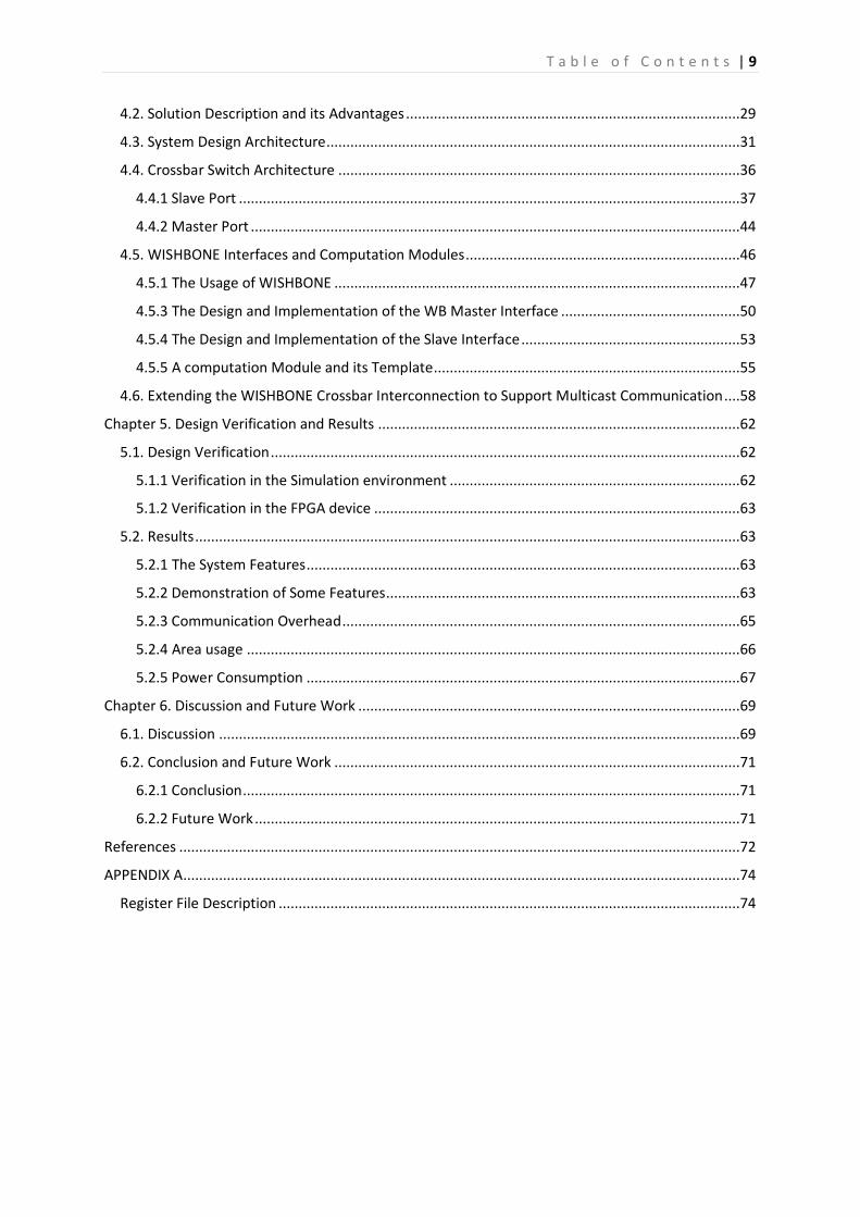
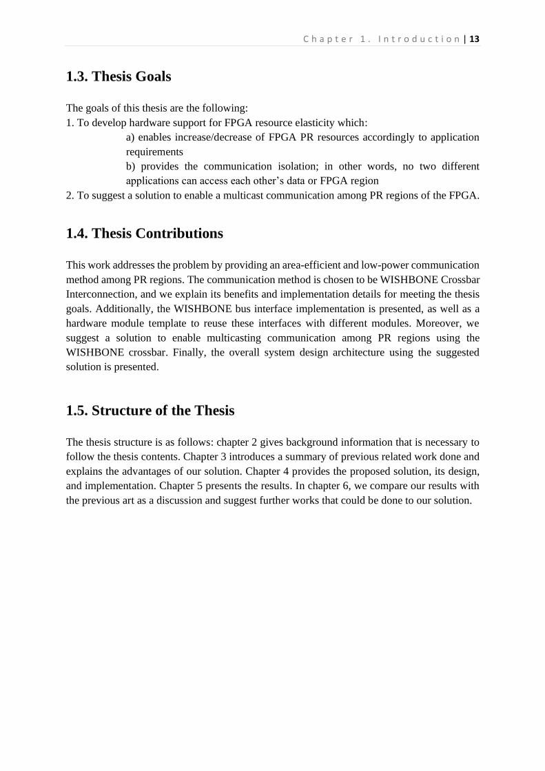
2.2.1 Network-on-Chip
Network-on-Chip (NoC) solutions apply the general idea of computer network topologies to
multichip systems as a communication method. To illustrate, each module is considered a node
and has a router; routers are connected following one network topology: mesh, torus, butterfly,
etc. The following figure 2.1 illustrates 3x3 NoC having mesh topology. The blue boxes
represent routers, while the red ones represent computation nodes.
Figure 2.1. 3x3 NoC with Mesh Topology
The communication flow is again similar to computer networks. First, a node directs its data to
its router, and the router divides data into packets and forwards them into the next router. Thus,
a packet travels through several routers until it reaches its destination. Routers can use routing
algorithms (random, weighted random, adaptive, etc.) or routing tables to decide which path to
follow [1].
Since there are multiple paths and routers available in network topology, parallel transmissions
can happen simultaneously. Therefore, this method improves latency and bandwidth problems
of shared-bus and P2P methods.
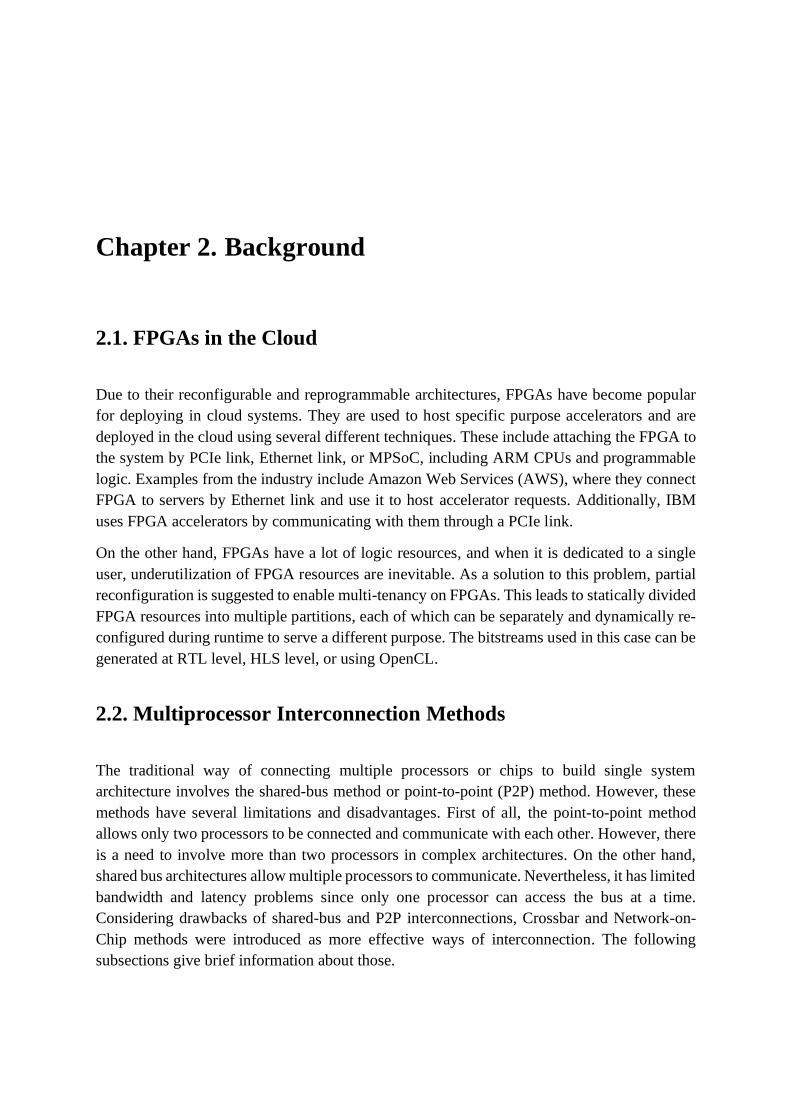
2.2.2 Crossbar Switch Interconnection
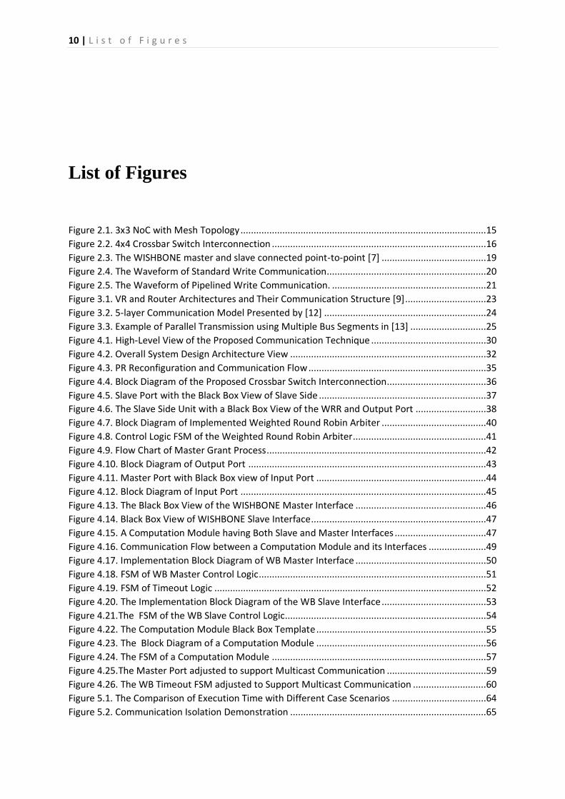
The crossbar switch interconnection consists of switches arranged in a matrix form and
connects the source module to a destination. As it is displayed in Figure 2.2, all modules are
connected to a common set of bus lines; however, communications are allowed or prevented
by switches illustrated as blue boxes. The communication request can be initiated by a master.
In the case of communication, switches are enabled to allow a physical connection between a
master and destination slave. Switches can be implemented using either transistors or
multiplexers.
16 | C h a p t e r 2 . B a c k g r o u n d
Figure 2.2. 4x4 Crossbar Switch Interconnection
Since there are separate bus lines for each destination, it is possible to do parallel transmissions
in a crossbar interconnection. The only limitation is that source devices must not target the
same destination. When they target the same destination, then arbitration logic is again applied
to regulate the access order.
2.3. PCIe Bus
PCIe Bus is a serial interconnect used for providing a physical communication link between
the CPU and FPGA [2]. It has several versions; however, the Gen3 version is used in this
project with a Xilinx Ultrascale+ device. PCIe Gen3 can support 16 lanes, each being 8-bit
wide, connected to the FPGA device. Consequently, it can support the transfer rate of 16 Giga
Transfer (GT)/sec. PCIe Bus is connected to GTH transceivers inside of the FPGA.
2.4. XDMA IP Core and Drivers
Xilinx provides DMA IP core [3] and specific XDMA drivers [4] in order to communicate with
Ultrascale+, Ultrascale, and Virtex FPGA device series from a host computer. FPGA device is
attached to a host PC by a GTH-PCIe link, connected to an XDMA IP core inside the FPGA.
Then the user data is delivered to the FPGA end running the XDMA driver application. The
following subsections provide a brief explanation about both the IP core and drivers.
2.4.1 XDMA IP Core [3]
As mentioned before, the IP core uses a GTH transceiver and PCIe link as a communication
link between a host PC and the FPGA. This link enables eight separate channels for a single
XDMA core to exchange data. The channels are called Host-to-Card (H2C) channels, which
C h a p t e r 2 . B a c k g r o u n d | 17
transmit data from the host computer to the FPGA, and Card-to-Host (C2H) channels, used for
transmitting data from the FPGA to the host computer. A single XDMA IP core can support
four H2C and four C2H channels.
Additionally, two options are provided as common communication interfaces to deliver data
from an XDMA to the user logic: the AXI Memory Mapped (AXI-MM) and AXI Streaming
(AXI-ST). When the AXI-MM interface is chosen, all H2C and C2H channels are connected
to a single interface accordingly. The AXI-ST interface, on the other hand, provides a separate
interface for each channel. Both interfaces can operate with a bit width up to 256 bits.
Furthermore, XDMA IP Core has two other channels. The first one enables a host to access a
user logic’s status and configuration registers; this is done through the AXI4-Lite Master
interface. Similarly, the user logic can access the DMA’s status and configuration registers
through the AXI4-Lite Slave interfaces. Those interfaces can support either 32-bit or 64-bit
read/write transactions. The other channel is used to bypass the DMA core and enables a host
to communicate with a user logic inside the FPGA directly. The bus width supported here is
32-bit and 64-bit, as well.
2.4.2 XDMA Drivers [4]
XDMA Drivers provide a simple way to deliver user data to the XDMA IP Core from a host
PC. It enables separate devices for each channel at a kernel level, making it convenient to use
them. For instance, xdma0_h2c_0 channel is used to transmit user data by the H2C-0 channel.
Similarly, xdma0_c2h_0 channel retrieves data from the FPGA device by the C2H-0 channel.
Additionally, xdma0_user channel is for using the AXI4-Lite interface of the XDMA IP core,
while xdma0_bypass channel is for bypassing XDMA. Finally, to get information about the
status of channels; if they are busy, completed transactions, etc., the debugging channel is
provided. This channel can retrieve information from the control and status register of the
XDMA IP core and is listed as xdma0_control device. More information about these
channels and debugging can be found at [4].
Furthermore, different functions are used to access each type of channel. Firstly, to transfer
data to the FPGA device using one of the H2C channels is done by dma_to_device function.
The general function prototype is:
./dma_to_device -d device -f file_name -s transaction_size_bytes -c
number_of_transactions
Executing the following command results in sending 1024 bytes from data.bin file two
times:
./dma_to_device -d /dev/xdma0_h2c_0 -f data.bin -s 1024 -c 2
Correspondingly, dma_from_device serves for getting data from the FPGA device:
./dma_from_device -d device -f file_name -s transaction_size_bytes -
c number_of_transactions
18 | C h a p t e r 2 . B a c k g r o u n d
The upcoming command reads 512 bytes from the FPGA using the first C2H channel to file
data_back.bin.
./dma_from_device -d /dev/xdma0_c2h_0 -f data_back.bin -s 512 -c 1
Moreover, the command to read or write from/to user logic’s registers by AXI4-Lite interface
reg_rw command is used:
./reg_rw device register_addr access_type
./reg_rw /dev/xdma0_user 0x0001 r
This command reads data from the register at the address of 0x0001.
XDMA drivers can operate in two different modes: polling mode and interrupt mode. In polling
mode, the host OS periodically keeps checking if there is any response from the XDMA IP
core. On the other hand, in the interrupt mode, whenever there is a response from the XDMA
IP core, an interrupt happens, followed by the OS kernel serving this interrupt. The XDMA
Drivers and the XDMA IP Core’s performances in different modes of the IP Core are provided
by [5]. The XDMA Drivers are available at [6].
2.5. WISHBONE Interconnection Architecture
WISHBONE Interconnection Architecture was invented by OpenCores and is targeted to
provide an effective communication method for IP cores on SoC [7]. According to [7], the
purpose is to increase the reusability of different IP cores in different communication scenarios
by providing a standard data exchange protocol. Since different IP cores have different I/O
ports, it is not always fast and simple to build a single design architecture connecting them. On
the other hand, using a standard bus interface and protocol for communication makes this
process easier.
WISHBONE Interconnection Architecture mainly consists of 2 parts: a bus protocol and the
communication interconnection. The bus protocol is a set of rules about exchanging data
among IPs and must be followed when designing bus interfaces. On the other hand,
communication interconnection is the way that IP cores are connected.
OpenCores does not specify the implementation of bus interfaces or interconnection
architectures. Instead, they provide a set of rules that should be followed in the design to be
suitable for a WISHBONE Interconnection architecture. Thus, implementation details are up
to a designer as long as it obeys this set of rules. The following sections provide a brief
background about the bus protocol and communication interconnections.
C h a p t e r 2 . B a c k g r o u n d | 19
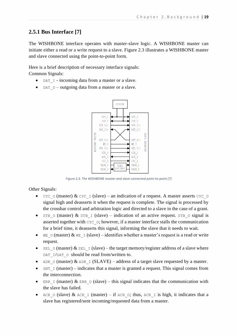
2.5.1 Bus Interface [7]
The WISHBONE interface operates with master-slave logic. A WISHBONE master can
initiate either a read or a write request to a slave. Figure 2.3 illustrates a WISHBONE master
and slave connected using the point-to-point form.
Here is a brief description of necessary interface signals:
Common Signals:
• DAT_I - incoming data from a master or a slave.
• DAT_O – outgoing data from a master or a slave.
Figure 2.3. The WISHBONE master and slave connected point-to-point [7]
Other Signals:
• CYC_O (master) & CYC_I (slave) – an indication of a request. A master asserts CYC_O
signal high and deasserts it when the request is complete. The signal is processed by
the crossbar control and arbitration logic and directed to a slave in the case of a grant.
• STB_O (master) & STB_I (slave) – indication of an active request. STB_O signal is
asserted together with CYC_O; however, if a master interface stalls the communication
for a brief time, it deasserts this signal, informing the slave that it needs to wait.
• WE_O (master) & WE_I (slave) – identifies whether a master’s request is a read or write
request.
• SEL_O (master) & SEL_I (slave) – the target memory/register address of a slave where
DAT_I/DAT_O should be read from/written to.
• ADR_O (master) & ADR_I (SLAVE) – address of a target slave requested by a master.
• GNT_I (master) – indicates that a master is granted a request. This signal comes from
the interconnection.
• ERR_I (master) & ERR_O (slave) – this signal indicates that the communication with
the slave has failed.
• ACK_O (slave) & ACK_I (master) – if ACK_O; thus, ACK_I is high, it indicates that a
slave has registered/sent incoming/requested data from a master.
20 | C h a p t e r 2 . B a c k g r o u n d
• STALL_O (slave) & STALL_I (master) – if STALL_O; thus, STALL_I is high, it indicates
that a slave has suspended the communication temporarily; a master needs to wait.
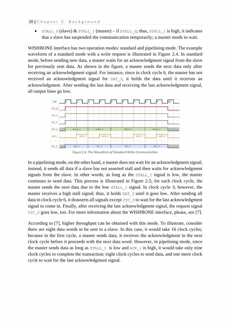
WISHBONE interface has two operation modes: standard and pipelining mode. The example
waveform of a standard mode with a write request is illustrated in Figure 2.4. In standard
mode, before sending new data, a master waits for an acknowledgment signal from the slave
for previously sent data. As shown in the figure, a master sends the next data only after
receiving an acknowledgment signal. For instance, since in clock cycle 6, the master has not
received an acknowledgment signal for DAT_3, it holds the data until it receives an
acknowledgment. After sending the last data and receiving the last acknowledgment signal,
all output lines go low.
Figure 2.4. The Waveform of Standard Write Communication
In a pipelining mode, on the other hand, a master does not wait for an acknowledgment signal;
instead, it sends all data if a slave has not asserted stall and then waits for acknowledgment
signals from the slave. In other words, as long as the STALL_I signal is low, the master
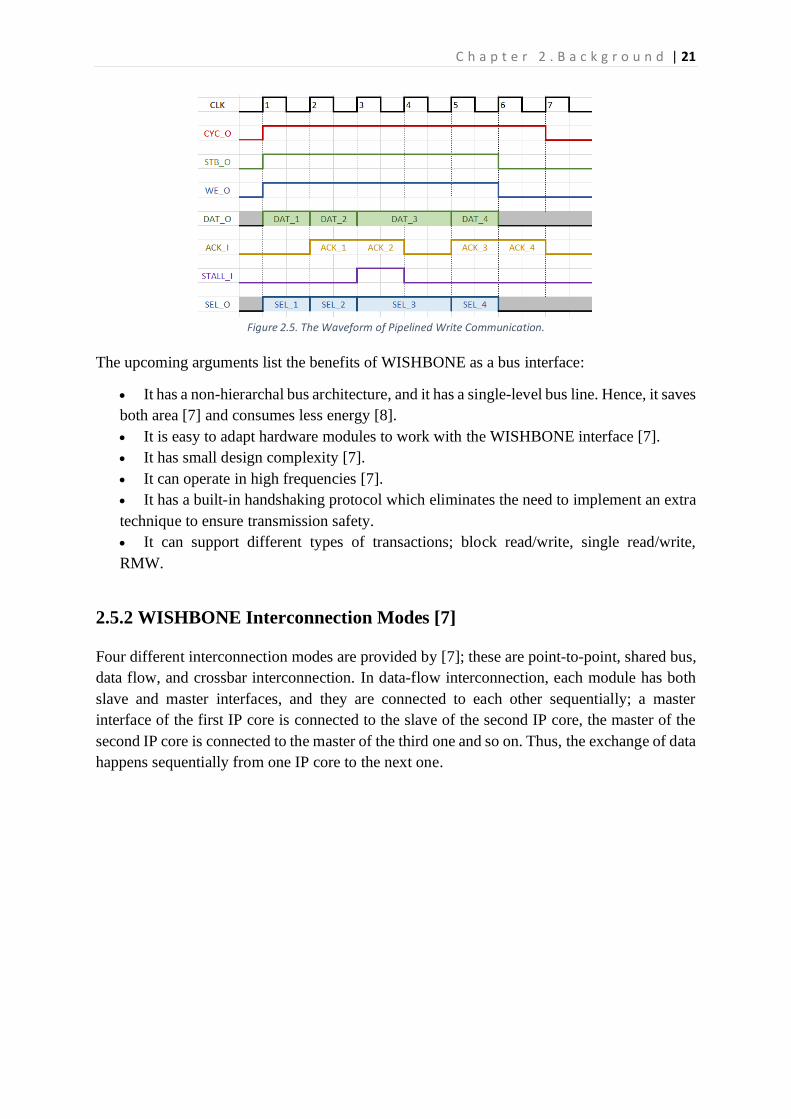
continues to send data. This process is illustrated in Figure 2.5; for each clock cycle, the
master sends the next data due to the low STALL_I signal. In clock cycle 3; however, the
master receives a high stall signal; thus, it holds DAT_3 until it goes low. After sending all
data in clock cycle 6, it deasserts all signals except CYC_O to wait for the last acknowledgment
signal to come in. Finally, after receiving the last acknowledgment signal, the request signal
CYC_O goes low, too. For more information about the WISHBONE interface, please, see [7].
According to [7], higher throughput can be obtained with this mode. To illustrate, consider
there are eight data words to be sent to a slave. In this case, it would take 16 clock cycles;
because in the first cycle, a master sends data, it receives the acknowledgment in the next
clock cycle before it proceeds with the next data word. However, in pipelining mode, since
the master sends data as long as STALL_I is low and ACK_I is high, it would take only nine
clock cycles to complete the transaction; eight clock cycles to send data, and one more clock
cycle to wait for the last acknowledgment signal.
C h a p t e r 2 . B a c k g r o u n d | 21
Figure 2.5. The Waveform of Pipelined Write Communication.
The upcoming arguments list the benefits of WISHBONE as a bus interface:
• It has a non-hierarchal bus architecture, and it has a single-level bus line. Hence, it saves
both area [7] and consumes less energy [8].
• It is easy to adapt hardware modules to work with the WISHBONE interface [7].
• It has small design complexity [7].
• It can operate in high frequencies [7].
• It has a built-in handshaking protocol which eliminates the need to implement an extra
technique to ensure transmission safety.
• It can support different types of transactions; block read/write, single read/write,
RMW.
2.5.2 WISHBONE Interconnection Modes [7]
Four different interconnection modes are provided by [7]; these are point-to-point, shared bus,
data flow, and crossbar interconnection. In data-flow interconnection, each module has both
slave and master interfaces, and they are connected to each other sequentially; a master
interface of the first IP core is connected to the slave of the second IP core, the master of the
second IP core is connected to the master of the third one and so on. Thus, the exchange of data
happens sequentially from one IP core to the next one.
Chapter 3. Related Work
Previous work on the FPGA elasticity mainly solves the problem by employing NoC
connections. Moreover, there are works done using a bitstream manipulation as well as shared
bus interconnection. The following sections highlight one work for each solution category and
provide their summaries. Additionally, the solution for the multicasting technique for the
selected bus interface is summarized, as well. The limitations of those works are listed in the
final subsection.
3.1. Architecture Support for FPGA Multi-tenancy in the Cloud [9]
This paper explores the problem of elasticity on FPGAs using the NoC solution. Authors
suggest that resources of the FPGA can be divided into virtual regions (VR), which are partially
reconfigurable. Then, they can communicate with one another using the NoC communication
method when needed. Initially, authors suggest a 3x3 mesh topology, each node having one
module – a partially reconfigurable region.
On the other hand, to decrease the area usage of routers, they apply some optimizations
techniques to routers and overall network. These optimizations include but are not restricted
to, firstly, implementing routers in a way that they do not contain any buffers; instead, buffers
are allocated inside of VRs. Additionally, routers are simplified so that they do not contain any
virtual channels (VCs) either since they are resource costly. Moreover, only 3-port routers are
used when there is no need for 4-port ones.
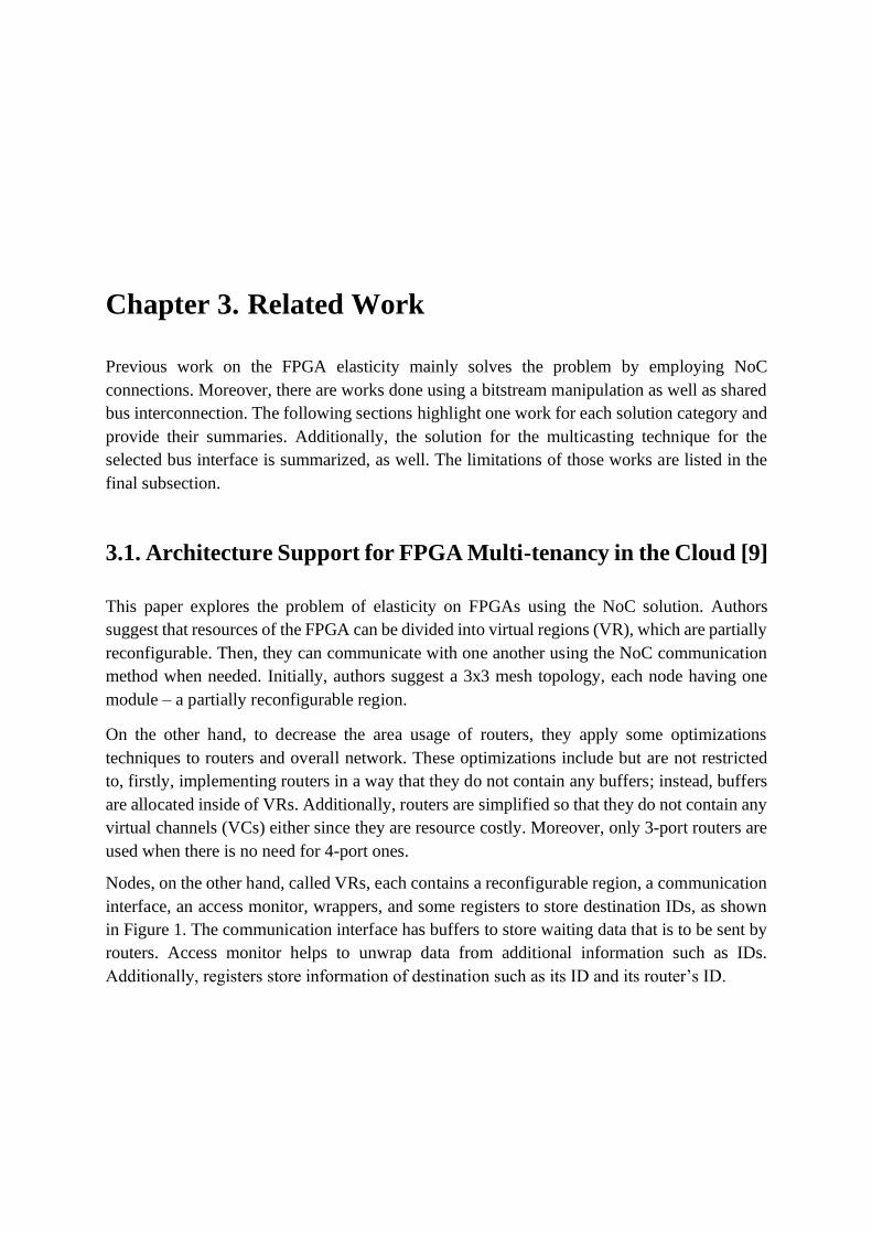
Nodes, on the other hand, called VRs, each contains a reconfigurable region, a communication
interface, an access monitor, wrappers, and some registers to store destination IDs, as shown
in Figure 1. The communication interface has buffers to store waiting data that is to be sent by
routers. Access monitor helps to unwrap data from additional information such as IDs.
Additionally, registers store information of destination such as its ID and its router’s ID.
C h a p t e r 3 . R e l a t e d W o r k | 23
Figure 3.1. VR and Router Architectures and Their Communication Structure [9]
The prototype of the proposed system was implemented in a 2x3 mesh having six modules
running. According to their results, optimizations show their impact on area usage; 3-port
routers take 305 LUTs, while 4-port routers take 495 LUTs. Moreover, since they have
eliminated buffers, routers do not take any BRAM sources. Overall, their NoC, together with
PR regions, takes 1.71 % of CLB resources on Xilinx Virtex Ultrascale+.
3.2. Resource Elastic Virtualization for FPGAs using OpenCL [10]
The researchers here approach the reconfiguration concept from an area time perspective of
view. Authors implement a resource manager which observes the currently available resources
of the FPGA and demanded applications, then decides when to run which application, how
many instances of it to run, and which version of it. To illustrate, each application has different
implementations taking a different number of resources in the reconfigurable area. Moreover,
when all resources are full and there are additional requests, time-division multiplexing (TDM)
is applied.
Firstly, to increase or decrease allocated FPGA resources to a specific PR region, they use the
BITMAN tool implemented by [11]. BITMAN tool takes the bitstream of the overall design
with initially allocated resources for applications, then manipulates the bitstream to change the
module's location, increase/decrease allocated resources, etc. Moreover, according to the
authors, the tool does not require any additional tools such as CAD; thus, being able to run on
general CPUs and microcontrollers.
Each application has different versions with different sizes and instances implemented in
OpenCL, referred to as kernels. The resource manager knows which applications are running
and which are being demanded to run. Then, the built-in scheduler decides which kernel and
its version to run based on both SDM and TDM. The decision flow is as follows: kernels and
their implementations are selected by the resource manager. Then resource allocation fairness
for each application is calculated based on the specific equations, which consider several
parameters, such as completion time of kernels, FPGA reconfiguration time, the size of
bitstreams, etc. Finally, the decision is given, which leads to a reconfiguration of the FPGA
with the selected kernel versions and the number of instances.
As a result of the resource manager prototype implemented, this application utilizes FPGA
resources 2.3x better and shows 49% better performance. Moreover, with the help of
scheduling algorithms, the average waiting times for kernels to be run are decreased, too.
24 | C h a p t e r 3 . R e l a t e d W o r k
3.3. A Design Methodology for Communication Infrastructures on
Partially Reconfigurable FPGAs [12]
In this paper, the authors introduce the specific design flow for reconfigurable architectures
called INDRA and implement the communication layer model to make reconfigurable regions
communicate. The details of INDRA are out of the scope of this work; thus, the presented
communication method is covered here only.
In the presented system architecture, a standard bus interface connects reconfigurable regions
to the common shared bus. Since the implemented shared bus architecture is a pipelined bus
architecture, although the bus interface of PR regions is WISHBONE, it is wrapped and
adapted to be able to support the pipelined bus; thus, called the Encapsulated WISHBONE
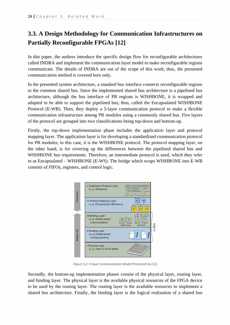
Protocol (E-WB). Then, they deploy a 5-layer communication protocol to make a flexible
communication infrastructure among PR modules using a commonly shared bus. Five layers
of the protocol are grouped into two classifications being top-down and bottom-up.
Firstly, the top-down implementation phase includes the application layer and protocol
mapping layer. The application layer is for developing a standardized communication protocol
for PR modules; in this case, it is the WISHBONE protocol. The protocol mapping layer, on
the other hand, is for covering up the differences between the pipelined shared bus and
WISHBONE bus requirements. Therefore, an intermediate protocol is used, which they refer
to as Encapsulated – WISHBONE (E-WS). The bridge which wraps WISHBONE into E-WB
consists of FIFOs, registers, and control logic.
Figure 3.2. 5-layer Communication Model Presented by [12]
Secondly, the bottom-up implementation phases consist of the physical layer, routing layer,
and binding layer. The physical layer is the available physical resources of the FPGA device
to be used by the routing layer. The routing layer is the available resources to implement a
shared bus architecture. Finally, the binding layer is the logical realization of a shared bus
C h a p t e r 3 . R e l a t e d W o r k | 25
architecture. Here they consider if the bus architecture should be implemented using a tri-state
buffer (TB-based) method or a slice-based method.
During the implementation part, the authors compare binding layer methods and summarize
the performance of the E-WB mapping. According to results, the slice-based communication
takes more area leaving less space for PR modules compared to the TB-based communication.
Coming to E-WB, it does not decrease WISHBONE’s original performance necessarily due to
its pipelined architecture. The results show that the protocol operates at 70 MHz for block
transfers larger than 1 KB with a 32-bit bus architecture.
3.4. A Practical Approach for Circuit Routing on Dynamic
Reconfigurable Devices [13]
In this paper, circuit routing method is researched as a communication method among
reconfigurable areas. The proposed technique relies on Reconfigurable Multiple Bus (RMB),
which was originally developed for multiprocessor systems communication [14], and it is
adapted to be used by 1-D and 2-D NoCs here. Authors want to eliminate the packet
communication method used by NoCs since it introduces extra communication overhead like
dividing data into packets, then combining and recovering original data at the destination. Thus,
they introduce Reconfigurable Multiple Bus on Chip (RMBoC) which provides a physical
communication link between a source and destination of NoCs’ nodes. Consequently, when a
physical channel is built then, a source can send its data directly to the destination without
communication overhead.
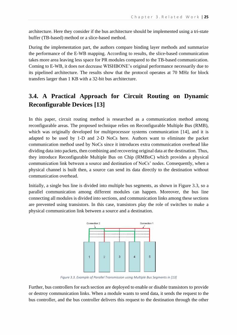
Initially, a single bus line is divided into multiple bus segments, as shown in Figure 3.3, so a
parallel communication among different modules can happen. Moreover, the bus line
connecting all modules is divided into sections, and communication links among these sections
are prevented using transistors. In this case, transistors play the role of switches to make a
physical communication link between a source and a destination.
Figure 3.3. Example of Parallel Transmission using Multiple Bus Segments in [13]
Further, bus controllers for each section are deployed to enable or disable transistors to provide
or destroy communication links. When a module wants to send data, it sends the request to the
bus controller, and the bus controller delivers this request to the destination through the other
26 | C h a p t e r 3 . R e l a t e d W o r k
bus controllers which sit on the path. Then if the destination is available, it sends a confirmation
reply, and this reply again propagates through all bus controllers. When each bus controller
receives this reply, they turn on transistors to recover the communication link. For each bus
controller, it takes eight clock cycles to process the request. Once the communication is built,
the latency of sending a message is one clock cycle only.
The implementation is done on the Virtex II 6000 FPGA device having four nodes hence four
bus controllers. According to results, in 1-D NoC, area overhead of RMBoC changes between
4-15% and max. reachable frequency is above 120 MHz. Additionally, the 2-D NoC version
also achieves high frequency – max. 95 MHz but takes 50% more area.
3.5. Enhancement of Wishbone Protocol with Broadcasting and
Multicasting [15]
This paper is reviewed for the WISHBONE protocol that is included in our solution, and we
are proposing a multicasting communication method involving it.
The solution suggested by the authors targets adding multicasting and broadcasting features to
WISHBONE shared bus interconnection. To do that, when a master is introduced to the system,
it assigns group IDs to slaves participating in multicasting, and slaves store their group IDs in
registers. Since slaves use registers to store group IDs, the number of groups they can belong
to is limited.
When multicasting happens, a master sends the group's ID as an address so that slaves can
check if they should participate in this communication. Then, all acknowledgment signal
responses from slaves are ANDed together and sent to the master. In this case, the slaves which
do not participate in this communication assert their acknowledgment signals unconditionally.
Eight slaves and four masters are implemented in the Nexys-4 board. The overall system
occupies 2566 LUTs and the operating frequency achieved is 207 MHz.
3.6. Limitations of Related Works
3.6.1 Limitations of Works on Resource Elasticity
NoC and Shared Bus Methods
Network-on-Chip method [1][16][17] or shared bus method [12] have the below-mentioned
disadvantages:
• The shared bus method is not a flexible or scalable method of communication due to its
bandwidth limitations. Here by flexibility, we refer to interconnection’s ability to support
different communication patterns. Additionally, scalability refers to interconnection’s
C h a p t e r 3 . R e l a t e d W o r k | 27
ability to be extended to support a larger number of modules. Although NoC architecture
is flexible and scalable, NoC’s area usage and power consumption are its big
disadvantages [8][18].
• The shared bus cannot support parallel transmissions. Although NoC provides a
parallel transmission feature, since NoC’s routers have a smaller number of physical
channels, it requires extra protocol overhead in order to handle access to them.
• NoC has a large network protocol overhead. This includes dividing a packet into
different segments, sending them separately, and recovering the original sequence in the
destination. Additionally, if any segment is lost, the source should send the whole packet
again.
Bitstream manipulation methods
The bitstream manipulation method for the resource elasticity is not flexible. In other words, it
is very device-specific because different FPGA devices have different bitstream file formatting.
Moreover, the BITMAN tool developed [11] is for specific devices, too. Additionally,
bitstream manipulation requires a very good understanding of the given device’s architecture
and its resources to be error safe. Finally, it is not assured that a bitstream file would be
available to a developer. Some vendors might prefer to provide encoded bitstream file format,
for instance.
3.6.2 Limitations of the Work on Multicast Communication Method
We use the WISHBONE Crossbar Interconnection as a communication method among PR
regions. There is no suggested way of multicasting for the WISHBONE protocol at all in the
WISHBONE datasheet. According to our research, there has not been work done for it
either except [15]. Nevertheless, the solution proposed by the authors in that paper is valid
for the shared bus interconnection. It would not work for the crossbar interconnection as the
grant process for the requested slaves is not the same. Additionally, this method has a
multicasting introduction overhead, such as assigning group IDs and forcing nonparticipant
slaves to assert acknowledgment signals. This would lead to extra traffic in the communication
path and disturbing unrelated slaves unnecessarily.
Chapter 4. Design and Implementation
4.1. Design Tools and Environment
4.1.1 Target Device
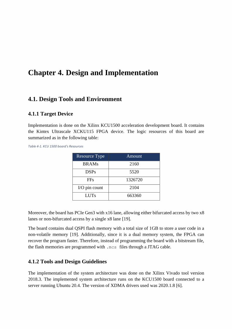
Implementation is done on the Xilinx KCU1500 acceleration development board. It contains
the Kintex Ultrascale XCKU115 FPGA device. The logic resources of this board are
summarized as in the following table:
Table 4-1. KCU 1500 board's Resources
Resource Type Amount
BRAMs 2160
DSPs 5520
FFs 1326720
I/O pin count 2104
LUTs 663360
Moreover, the board has PCIe Gen3 with x16 lane, allowing either bifurcated access by two x8
lanes or non-bifurcated access by a single x8 lane [19].
The board contains dual QSPI flash memory with a total size of 1GB to store a user code in a
non-volatile memory [19]. Additionally, since it is a dual memory system, the FPGA can
recover the program faster. Therefore, instead of programming the board with a bitstream file,
the flash memories are programmed with .mcs files through a JTAG cable.
4.1.2 Tools and Design Guidelines
The implementation of the system architecture was done on the Xilinx Vivado tool version
2018.3. The implemented system architecture runs on the KCU1500 board connected to a
server running Ubuntu 20.4. The version of XDMA drivers used was 2020.1.8 [6].
C h a p t e r 4 . D e s i g n a n d I m p l e m e n t a t i o n | 29
Additionally, we also make use of Xilinx-developed IP cores: XDMA core, ICAP, and FIFOs.
The crossbar interconnection and other hardware components; AXI-WB, WB-AXI modules,
the register file, bus interfaces, and computation modules in the overall system architecture are
developed using VHDL. Those components are made available in the user repository of Vivado
by custom IP packaging.
The suggested system architecture contains the ICAP module to enable the partial
reconfiguration feature of the FPGA device; however, in the implementation it is not used.
Instead, the developed crossbar interconnection, bus interfaces, and their features are tested
using statically allocated modules. Enabling the reconfiguration feature of the FPGA and
reprograming it dynamically through the PCIe link and ICAP module, as is suggested in the
solution, has been done by [5].
4.2. Solution Description and its Advantages
The main idea of the proposed solution is to divide an application’s request into small
computational modules and accelerate those modules to small-sized PR regions. Then, these
modules communicate with one another to exchange computation results using the
communication technique. Utterly, since an application is divided into small computational
modules and PR regions are small-sized, the underutilization of resources is decreased. On the
other hand, allocating extra PR regions if needed and enabling them to communicate can
increase the number of allocated resources to the application. Nevertheless, originally PR
regions are isolated from each other; therefore, the challenge occurs on how to make them
communicate.
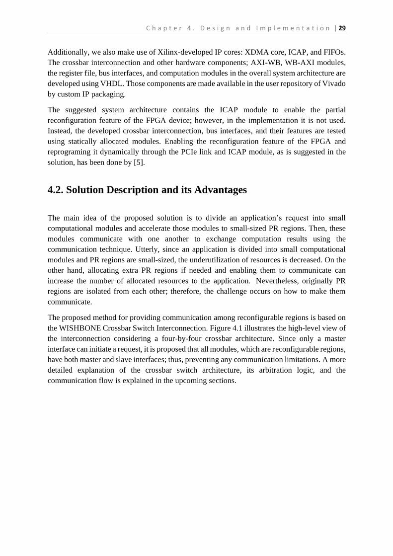
The proposed method for providing communication among reconfigurable regions is based on
the WISHBONE Crossbar Switch Interconnection. Figure 4.1 illustrates the high-level view of
the interconnection considering a four-by-four crossbar architecture. Since only a master
interface can initiate a request, it is proposed that all modules, which are reconfigurable regions,
have both master and slave interfaces; thus, preventing any communication limitations. A more
detailed explanation of the crossbar switch architecture, its arbitration logic, and the
communication flow is explained in the upcoming sections.
30 | C h a p t e r 4 . D e s i g n a n d I m p l e m e n t a t i o n
Figure 4.1. High-Level View of the Proposed Communication Technique
Using a crossbar architecture has the below-mentioned benefits:
• A crossbar switch interconnection is more flexible and scalable than a shared bus
architecture; however, less than NoC. Both scalability and flexibility come with the
area overhead; the more flexible or scalable, the more area usage. Crossbar
interconnection has more area usage than a shared bus [7][8][20] but less than NoC. In
other words, it stays in the middle of the area and flexibility/scalability tradeoff.
• A crossbar interconnection’s main area usage comes from its arbitration logic [20]. The
arbiter of a crossbar interconnection must observe multiple channels; thus, requiring
more complex logic. Auspiciously, it is possible to decrease the area usage of the
crossbar by optimizing its arbitration logic [21] and we use the suggested method in
[21] and further design optimizations to implement an area-friendly arbiter.
• A crossbar interconnection can support multiple transmissions in parallel while not
having the overhead problem to handle physical channels as in NoC.
• A crossbar interconnection does not have network protocol overhead once the
communication channel is established in contrast to NoC. In crossbar architecture,
when the physical communication channel is enabled between modules, the whole data
can be transmitted using this channel. However, in NoC architecture different packets
of the same data follow different paths and require to be retrieved in the correct order
in the destination.
• A crossbar interconnection can demonstrate good performance on different types of
scenarios. According to [22], the performance of communication architectures depends
on the communication pattern. In other words, it can be a pipelined communication in
which modules send data to the next ones sequentially. Yet, a communication pattern
C h a p t e r 4 . D e s i g n a n d I m p l e m e n t a t i o n | 31
can be global; each module shares data with any of the other modules. A crossbar
architecture shows adequate latency and throughput results in both scenarios.
Additionally, the main reason for using WISHBONE bus interface is to increase the reusability
of the crossbar architecture. In other words, the goal is to make different IP cores to be easily
adapted to the interconnection through a standard bus interface. Combining the advantages of
crossbar and WISHBONE interface, adjusting, and modifying their futures to support
communication among PR regions, our proposed solution:
• enables dynamically increasing/decreasing FPGA PR region resources allocated to
the application.
• provides an easy way of managing the communication isolation for different user
requests.
• provides a simpler way of handling dynamic bandwidth allocation inside the FPGA
device.
• has a low area usage due to the optimized way of implementation.
• has low communication protocol overhead.
• is flexible to be used with different hardware modules due to the usage of the
standard bus interface.
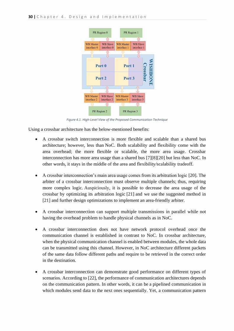
4.3. System Design Architecture
This section describes how the proposed solution will be used as a part of the overall system
architecture with PR regions. Figure 4.2 displays the system architecture that will be
implemented. The purposes of other essential components follow:
FPGA Elastic Resource Manager
User requests are sent to the FPGA Elastic Resource Manager, which has to keep track of the
PR regions. It knows which PR regions are available and which PR regions the specific user’s
application is using. Therefore, when it receives a request, it analyzes a request in terms of
required PR regions to handle it and then program the FPGA accordingly. Furthermore, it
also sends user data to PR regions, provides configuration information, and recovers status
information from the register file. The FPGA Elastic Resource Manager achieves these tasks
utilizing the XDMA Driver, PCIe express cable, and XDMA IP Core. The work flow of the
resource manager in different scenarios is explained in Communication Flow section and
illustrated in Figure 4.3.
The XDMA IP Core
The AXI-ST interface of the XDMA IP core is used due to simplified access to the ICAP
module. Since the AXI-ST enables to use each channel of the XDMA, it is possible to dedicate
a separate link to the ICAP module. On the other hand, the AXI-Lite bypass link of the XDMA
IP is used to access the register file.
32 | C h a p t e r 4 . D e s i g n a n d I m p l e m e n t a t i o n
ICAP
The ICAP module does programming of PR regions. To decrease reconfiguration overhead, in
other words, to enable a fast reconfiguration process, the ICAP module is connected through
the dedicated link - H2C3 from the XDMA IP core. Additionally, the ICAP module operates
at the clock frequency of 125 MHz while the rest of the system has 250 MHz. Therefore, to
prevent the loss of information due to different clock speeds, a FIFO buffer is added before the
ICAP module.
Register File
The register file plays an important role in providing configuration data and storing necessary
status information. Firstly, when ICAP reconfigures PR regions, it stores the status data on the
register file regarding whether the reconfiguration process was successful or failed. Secondly,
the WB Crossbar switch and PR regions are served by the register file, too. For the crossbar,
the purpose of having the register file is to provide the requested bandwidth to applications and
to enable the communication isolation. The crossbar operates with a weighted round-robin
technique; thus, it needs to know how many packages each module can send the other one.
Furthermore, the crossbar must know which modules are allowed to communicate with each
other. On the other hand, each computation module must know what its destination address is.
This kind of information is stored in the register file as configuration data. Moreover, when a
computation module’s attempt to make a communication fails either due to a wrong destination
address or timeout due to an unresponsive destination, those error codes are registered in the
Figure 4.2. Overall System Design Architecture View
C h a p t e r 4 . D e s i g n a n d I m p l e m e n t a t i o n | 33
register file as status data. Finally, before PR regions are reprogrammed, they should be reset
in order to prevent them from making any possible communication with the other modules
during the reconfiguration process. These reset signals are provided through the register file,
too.
The access to the register file by the user space, either to write configuration data or to read
any status data, is done through the AXI Lite interface of the XDMA IP Core. The reason for
this choice is that this interface is a bypass interface which means it enables easy and simple
access to the register file. Moreover, it prevents interference between register file data and other
user data for computations since they are done in different channels. The contents and addresses
of the register file are given in Table A.1. in APPENDIX A.
AXI-to-WB and WB-to-AXI
Finally, in order to deliver user data for computations, one of the crossbar’s ports is used
together with the AXI-to-WB and WB-to-AXI modules. First, user data is stored in FIFO
buffers together with its application ID through H2C-0 to H2C-2 channels; each channel has a
dedicated FIFO. The allocation of channels is not static, meaning that any application data can
be sent through any H2C channel and similarly, can be read back through any C2H channel.
The AXI-to-WB module serves each FIFO periodically. Since FIFO channels have AXI
interfaces, the implemented WISHBONE master interface here also has an AXI interface;
hence, making the AXI-to-WB module. The same principle is valid for the WISHBONE slave
interface side, too. When it receives computation results from the modules, it sends results to
one of the C2H channels through the AXI-Streaming interface. It accesses each channel
periodically one by one. This module is referred to as WB-to-AXI in Figure 2.
In the AXI-to-WB module, the WISHBONE master delivers user data to the destined PR region
based on the application ID. It knows the destination module of each application through the
register file. The reason for using the application ID instead of a direct destination address is
to prevent other applications from accessing invalid locations. To clarify, the crossbar port
which serves for delivering/reading user data is allowed to access any PR regions since it must
provide necessary computation data of all user applications and read back its results. Thus,
some other applications may try to access an invalid location by providing the wrong
destination address. Nevertheless, using the application ID here, the WISHBONE master
directs the data to a valid destination with the help of the register file. It should be noted that,
as the implemented version of a crossbar has four ports and one of the ports is dedicated to the
PCIe link, the number of PR regions here is three.
Clock System
The ICAP module operates with a 125 MHz frequency. On the other hand, the rest of the
modules operates with a 250 MHz frequency. The PCIe reference clock of 100 MHz is buffered
and fed into the XDMA IP core. Then, the XDMA IP core generates a 250 MHz frequency
connected to the rest of the modules. Since in this implementation, we use statically allocated
modules, not PR modules, this method is applicable here.
34 | C h a p t e r 4 . D e s i g n a n d I m p l e m e n t a t i o n
Reset System
All computation modules, as well as the crossbar interconnection, have both local and global
resets. The global reset is used to reset the whole system architecture at once. To do so, the
asynchronous reset signal of the XDMA IP core is buffered and connected to the modules. On
the other hand, the local reset signals are provided by the register file. Each local reset signal
is sent to a computation module and to the crossbar port where that module is connected; thus,
enabling to reset a specific resource and its configurations. Locally resetting is also useful when
ICAP does the reconfiguration process; the module can be isolated from the rest of the system,
and the crossbar port would be prevented from making any grant decisions.
Communication Flow
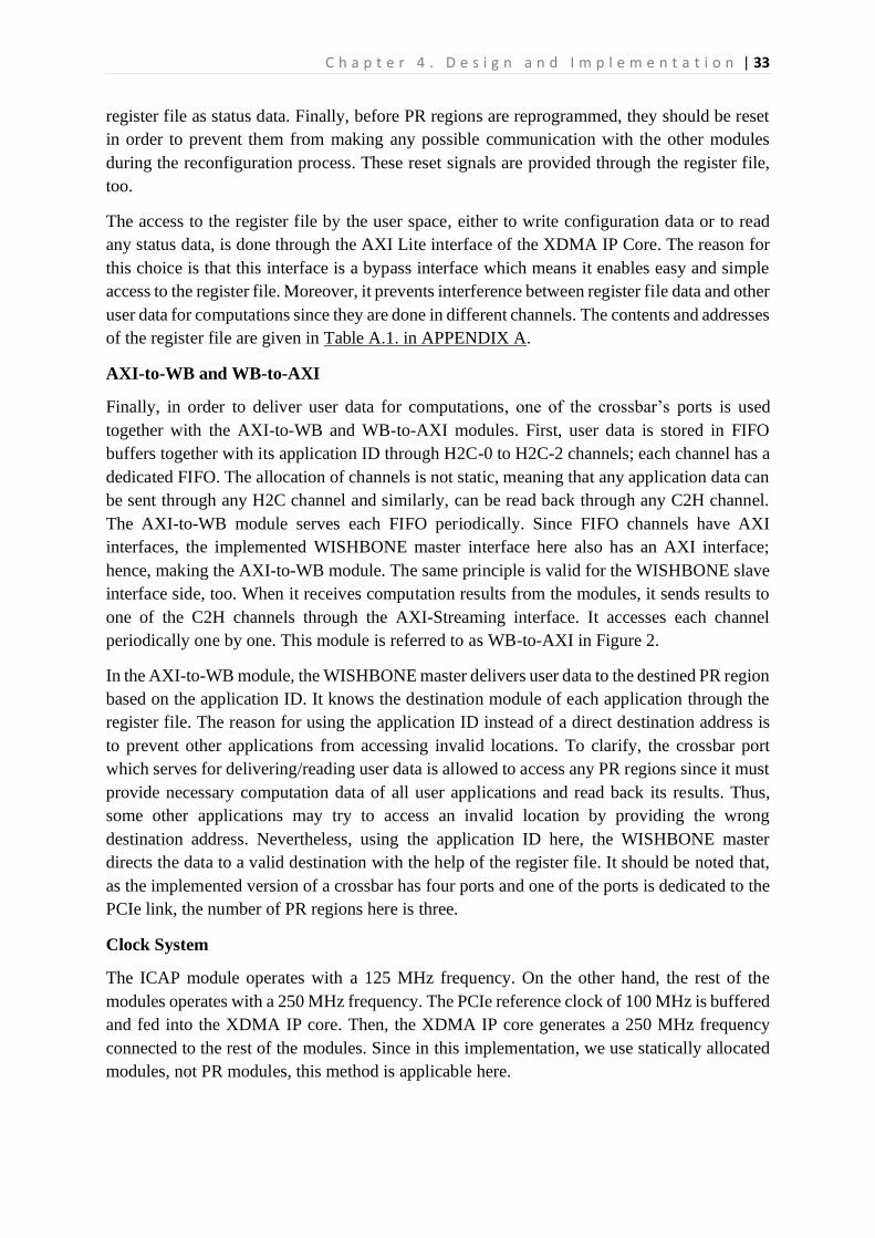
Figure 4.3 shows a flow diagram of the whole process of reconfiguration and providing elastic
resources to the application. To sum up, a user sends a request to the FPGA Elastic Resource
Manager. The manager allocates the available amount of PR regions to the application’s
computation modules through the ICAP. If there are not enough PR regions to host all modules,
part of them runs on the server (referred to as on-server module from now on), which means
they are not accelerated to the FPGA. Then, the manager provides configuration data to PR
regions and the crossbar (allowed modules, destination modules, and allowed number of
packages). In this phase, the last module’s destination address is set back to the server to receive
its results and continue the computation on the server. Afterward, it sends user data to start the
computation process. When the on-server module finishes its computation, the FPGA manager
checks again if there are any PR regions released so that it can run the on-server module on the
FPGA, as well. If so, then it reprograms the available PR region with the on-server module and
updates the other module’s destination addresses so that they communicate with the newly
available module, as well. Thus, resource elasticity is achieved; the allocated resource for the
user is increased by the communication interconnection among PR regions.
C h a p t e r 4 . D e s i g n a n d I m p l e m e n t a t i o n | 35
Figure 4.3. PR Reconfiguration and Communication Flow
36 | C h a p t e r 4 . D e s i g n a n d I m p l e m e n t a t i o n
4.4. Crossbar Switch Architecture
This section explains how the proposed crossbar architecture has been designed and
implemented. The novelty in this section includes designing a crossbar that can provide the
communication isolation and dynamic bandwidth allocation. Moreover, applying the
suggested optimized way of designing a round-robin arbiter to implement weighted round-
robin is included.
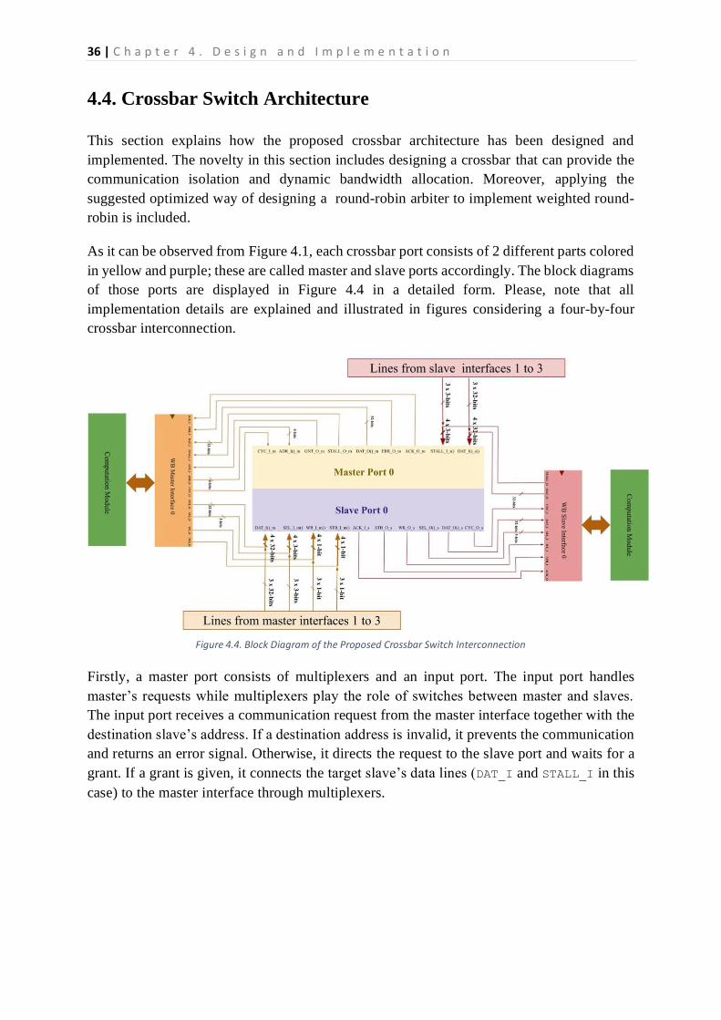
As it can be observed from Figure 4.1, each crossbar port consists of 2 different parts colored
in yellow and purple; these are called master and slave ports accordingly. The block diagrams
of those ports are displayed in Figure 4.4 in a detailed form. Please, note that all
implementation details are explained and illustrated in figures considering a four-by-four
crossbar interconnection.
Figure 4.4. Block Diagram of the Proposed Crossbar Switch Interconnection
Firstly, a master port consists of multiplexers and an input port. The input port handles
master’s requests while multiplexers play the role of switches between master and slaves.
The input port receives a communication request from the master interface together with the
destination slave’s address. If a destination address is invalid, it prevents the communication
and returns an error signal. Otherwise, it directs the request to the slave port and waits for a
grant. If a grant is given, it connects the target slave’s data lines (DAT_I and STALL_I in this
case) to the master interface through multiplexers.
C h a p t e r 4 . D e s i g n a n d I m p l e m e n t a t i o n | 37
A slave port, on the other hand, is responsible for giving grants based on requests coming
from master ports. It also keeps track of exchanged package numbers between the slave and
a master. Additionally, it sends grant signals back to a master and enables the slave to initiate
communication. Finally, it connects the granted master’s data signals (DAT_I, SEL_I,
STB_I, and WR_I in this case) to the slave interface through multiplexers. A slave port
consists of an arbitration logic and output port module - called the slave side together, and
multiplexers to achieve these tasks. This also implies that an arbitration logic in this crossbar
architecture is decentralized, meaning each slave has its own arbiter to serve masters. The
benefits of this design choice and each component are explained in detail in the upcoming
sections.
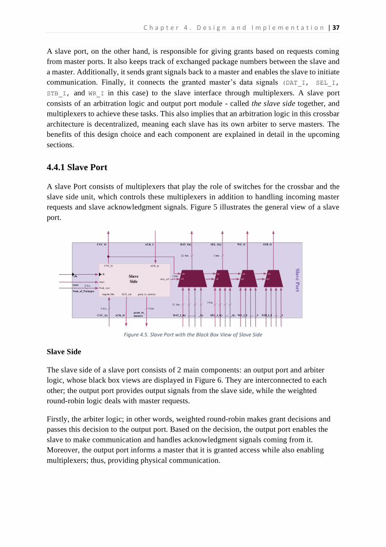
4.4.1 Slave Port
A slave Port consists of multiplexers that play the role of switches for the crossbar and the
slave side unit, which controls these multiplexers in addition to handling incoming master
requests and slave acknowledgment signals. Figure 5 illustrates the general view of a slave
port.
Figure 4.5. Slave Port with the Black Box View of Slave Side
Slave Side
The slave side of a slave port consists of 2 main components: an output port and arbiter
logic, whose black box views are displayed in Figure 6. They are interconnected to each
other; the output port provides output signals from the slave side, while the weighted
round-robin logic deals with master requests.
Firstly, the arbiter logic; in other words, weighted round-robin makes grant decisions and
passes this decision to the output port. Based on the decision, the output port enables the
slave to make communication and handles acknowledgment signals coming from it.
Moreover, the output port informs a master that it is granted access while also enabling
multiplexers; thus, providing physical communication.
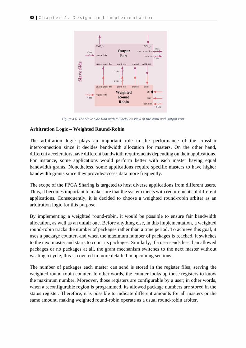
38 | C h a p t e r 4 . D e s i g n a n d I m p l e m e n t a t i o n
Figure 4.6. The Slave Side Unit with a Black Box View of the WRR and Output Port
Arbitration Logic – Weighted Round-Robin
The arbitration logic plays an important role in the performance of the crossbar
interconnection since it decides bandwidth allocation for masters. On the other hand,
different accelerators have different bandwidth requirements depending on their applications.
For instance, some applications would perform better with each master having equal
bandwidth grants. Nonetheless, some applications require specific masters to have higher
bandwidth grants since they provide/access data more frequently.
The scope of the FPGA Sharing is targeted to host diverse applications from different users.
Thus, it becomes important to make sure that the system meets with requirements of different
applications. Consequently, it is decided to choose a weighted round-robin arbiter as an
arbitration logic for this purpose.
By implementing a weighted round-robin, it would be possible to ensure fair bandwidth
allocation, as well as an unfair one. Before anything else, in this implementation, a weighted
round-robin tracks the number of packages rather than a time period. To achieve this goal, it
uses a package counter, and when the maximum number of packages is reached, it switches
to the next master and starts to count its packages. Similarly, if a user sends less than allowed
packages or no packages at all, the grant mechanism switches to the next master without
wasting a cycle; this is covered in more detailed in upcoming sections.
The number of packages each master can send is stored in the register files, serving the
weighted round-robin counter. In other words, the counter looks up those registers to know
the maximum number. Moreover, those registers are configurable by a user; in other words,
when a reconfigurable region is programmed, its allowed package numbers are stored in the
status register. Therefore, it is possible to indicate different amounts for all masters or the
same amount, making weighted round-robin operate as a usual round-robin arbiter.
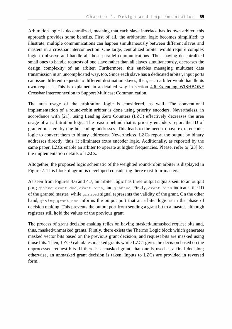
C h a p t e r 4 . D e s i g n a n d I m p l e m e n t a t i o n | 39
Arbitration logic is decentralized, meaning that each slave interface has its own arbiter; this
approach provides some benefits. First of all, the arbitration logic becomes simplified; to
illustrate, multiple communications can happen simultaneously between different slaves and
masters in a crossbar interconnection. One large, centralized arbiter would require complex
logic to observe and handle all those parallel communications. Thus, having decentralized
small ones to handle requests of one slave rather than all slaves simultaneously, decreases the
design complexity of an arbiter. Furthermore, this enables managing multicast data
transmission in an uncomplicated way, too. Since each slave has a dedicated arbiter, input ports
can issue different requests to different destination slaves; then, each arbiter would handle its
own requests. This is explained in a detailed way in section 4.6 Extending WISHBONE
Crossbar Interconnection to Support Multicast Communication.
The area usage of the arbitration logic is considered, as well. The conventional
implementation of a round-robin arbiter is done using priority encoders. Nevertheless, in
accordance with [21], using Leading Zero Counters (LZC) effectively decreases the area
usage of an arbitration logic. The reason behind that is priority encoders report the ID of
granted masters by one-hot-coding addresses. This leads to the need to have extra encoder
logic to convert them to binary addresses. Nevertheless, LZCs report the output by binary
addresses directly; thus, it eliminates extra encoder logic. Additionally, as reported by the
same paper, LZCs enable an arbiter to operate at higher frequencies. Please, refer to [23] for
the implementation details of LZCs.
Altogether, the proposed logic schematic of the weighted round-robin arbiter is displayed in
Figure 7. This block diagram is developed considering there exist four masters.
As seen from Figures 4.6 and 4.7, an arbiter logic has three output signals sent to an output
port; giving_grant_dec, grant_bits, and granted. Firstly, grant_bits indicates the ID
of the granted master, while granted signal represents the validity of the grant. On the other
hand, giving_grant_dec informs the output port that an arbiter logic is in the phase of
decision making. This prevents the output port from sending a grant bit to a master, although
registers still hold the values of the previous grant.
The process of grant decision-making relies on having masked/unmasked request bits and,
thus, masked/unmasked grants. Firstly, there exists the Thermo Logic block which generates
masked vector bits based on the previous grant decision, and request bits are masked using
those bits. Then, LZC0 calculates masked grants while LZC1 gives the decision based on the
unprocessed request bits. If there is a masked grant, that one is used as a final decision;
otherwise, an unmasked grant decision is taken. Inputs to LZCs are provided in reversed
form.
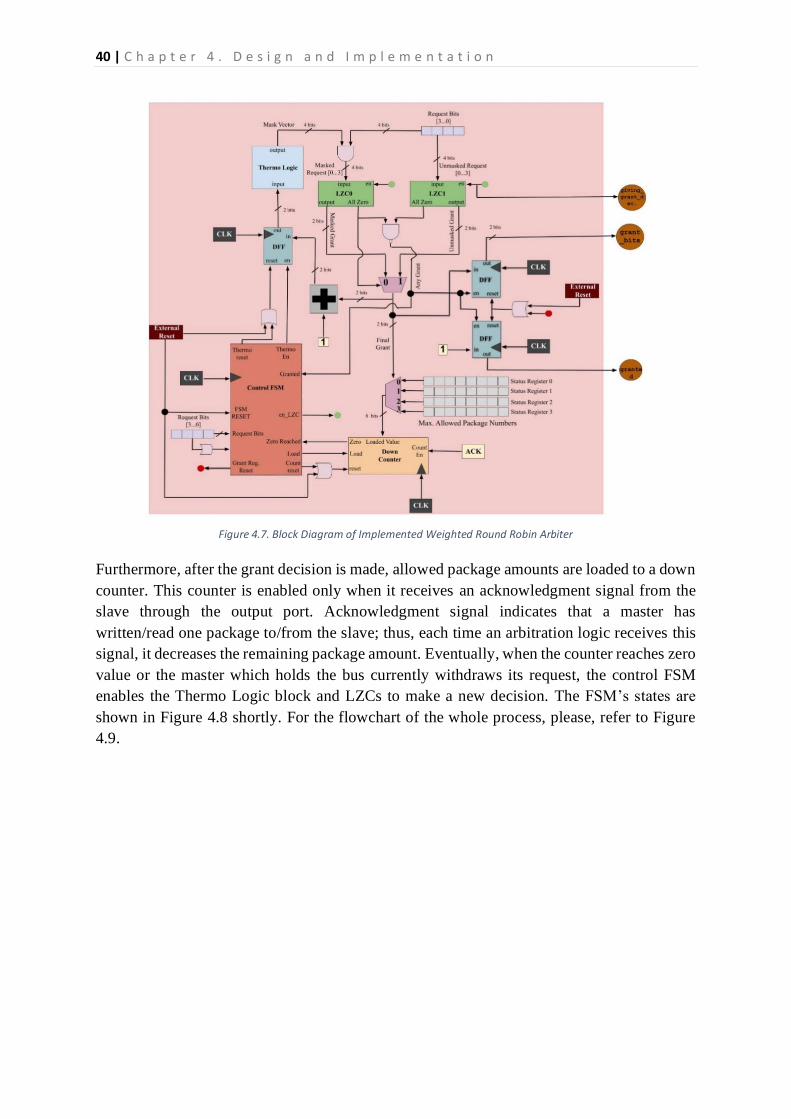
40 | C h a p t e r 4 . D e s i g n a n d I m p l e m e n t a t i o n
Figure 4.7. Block Diagram of Implemented Weighted Round Robin Arbiter
Furthermore, after the grant decision is made, allowed package amounts are loaded to a down
counter. This counter is enabled only when it receives an acknowledgment signal from the
slave through the output port. Acknowledgment signal indicates that a master has
written/read one package to/from the slave; thus, each time an arbitration logic receives this
signal, it decreases the remaining package amount. Eventually, when the counter reaches zero
value or the master which holds the bus currently withdraws its request, the control FSM
enables the Thermo Logic block and LZCs to make a new decision. The FSM’s states are
shown in Figure 4.8 shortly. For the flowchart of the whole process, please, refer to Figure
4.9.
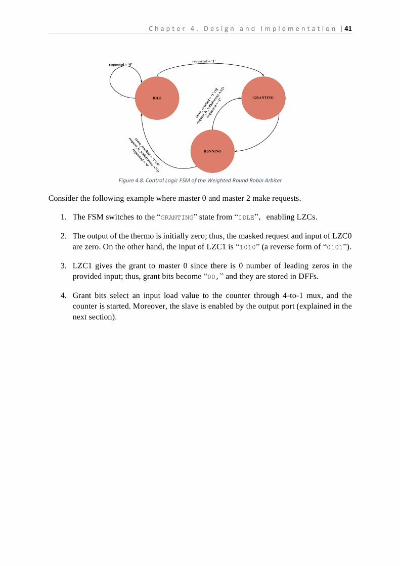
C h a p t e r 4 . D e s i g n a n d I m p l e m e n t a t i o n | 41
Figure 4.8. Control Logic FSM of the Weighted Round Robin Arbiter
Consider the following example where master 0 and master 2 make requests.
1. The FSM switches to the “GRANTING” state from “IDLE”, enabling LZCs.
2. The output of the thermo is initially zero; thus, the masked request and input of LZC0
are zero. On the other hand, the input of LZC1 is “1010” (a reverse form of “0101”).
3. LZC1 gives the grant to master 0 since there is 0 number of leading zeros in the
provided input; thus, grant bits become “00,” and they are stored in DFFs.
4. Grant bits select an input load value to the counter through 4-to-1 mux, and the
counter is started. Moreover, the slave is enabled by the output port (explained in the
next section).
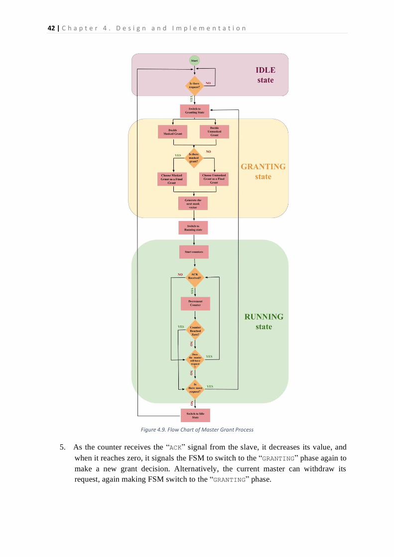
42 | C h a p t e r 4 . D e s i g n a n d I m p l e m e n t a t i o n
Figure 4.9. Flow Chart of Master Grant Process
5. As the counter receives the “ACK” signal from the slave, it decreases its value, and
when it reaches zero, it signals the FSM to switch to the “GRANTING” phase again to
make a new grant decision. Alternatively, the current master can withdraw its
request, again making FSM switch to the “GRANTING” phase.
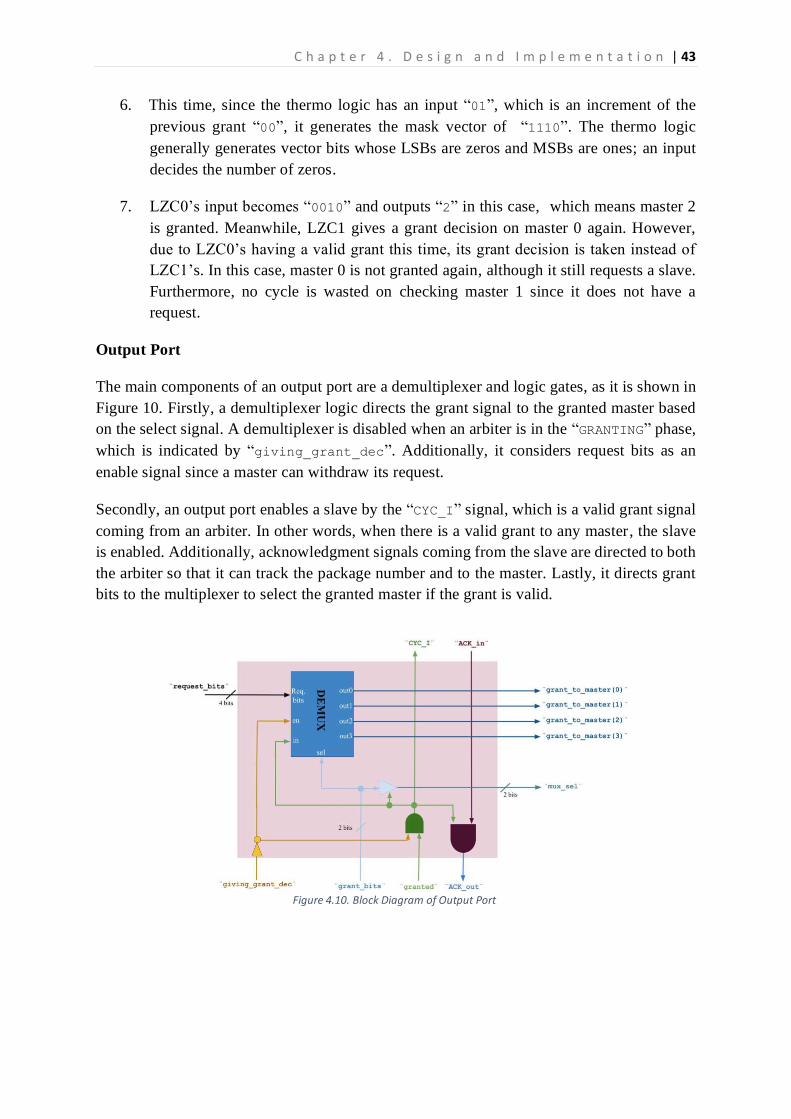
C h a p t e r 4 . D e s i g n a n d I m p l e m e n t a t i o n | 43
6. This time, since the thermo logic has an input “01”, which is an increment of the
previous grant “00”, it generates the mask vector of “1110”. The thermo logic
generally generates vector bits whose LSBs are zeros and MSBs are ones; an input
decides the number of zeros.
7. LZC0’s input becomes “0010” and outputs “2” in this case, which means master 2
is granted. Meanwhile, LZC1 gives a grant decision on master 0 again. However,
due to LZC0’s having a valid grant this time, its grant decision is taken instead of
LZC1’s. In this case, master 0 is not granted again, although it still requests a slave.
Furthermore, no cycle is wasted on checking master 1 since it does not have a
request.
Output Port
The main components of an output port are a demultiplexer and logic gates, as it is shown in
Figure 10. Firstly, a demultiplexer logic directs the grant signal to the granted master based
on the select signal. A demultiplexer is disabled when an arbiter is in the “GRANTING” phase,
which is indicated by “giving_grant_dec”. Additionally, it considers request bits as an
enable signal since a master can withdraw its request.
Secondly, an output port enables a slave by the “CYC_I” signal, which is a valid grant signal
coming from an arbiter. In other words, when there is a valid grant to any master, the slave
is enabled. Additionally, acknowledgment signals coming from the slave are directed to both
the arbiter so that it can track the package number and to the master. Lastly, it directs grant
bits to the multiplexer to select the granted master if the grant is valid.
Figure 4.10. Block Diagram of Output Port

44 | C h a p t e r 4 . D e s i g n a n d I m p l e m e n t a t i o n
4.4.2 Master Port
A master Port, as it is displayed in Figure 4.11, includes a switch for data lines and an input
port to manage a master’s requests, grant signals, acknowledgment signals while also
providing communication isolation. A switch is a 4-to-1 multiplexer that selects among
incoming slave data lines. The input port provides the multiplexer’s select signal and enable
signal. There could have been separate multiplexers to select among grant and
acknowledgment signals, too, instead of directing them to an input port. However, since there
will be multicasting communication, handling those signals inside an input port is more
appropriate.
Input Ports
As it is mentioned above, an input port is in charge of handling a master’s requests. First of all,
it checks if the request is valid, meaning that the master does not try to access a forbidden slave
(the communication isolation), and only then, the request should proceed further. Figure 4.12
shows the implemented block diagram of an input port. The implemented version does not
include a multicasting technique. However, the suggested solution to enable multicasting will
be explained in the upcoming section 4.6 Extending WISHBONE Crossbar Interconnection to
Support Multicast Communication.
Figure 4.11. Master Port with Black Box view of Input Port
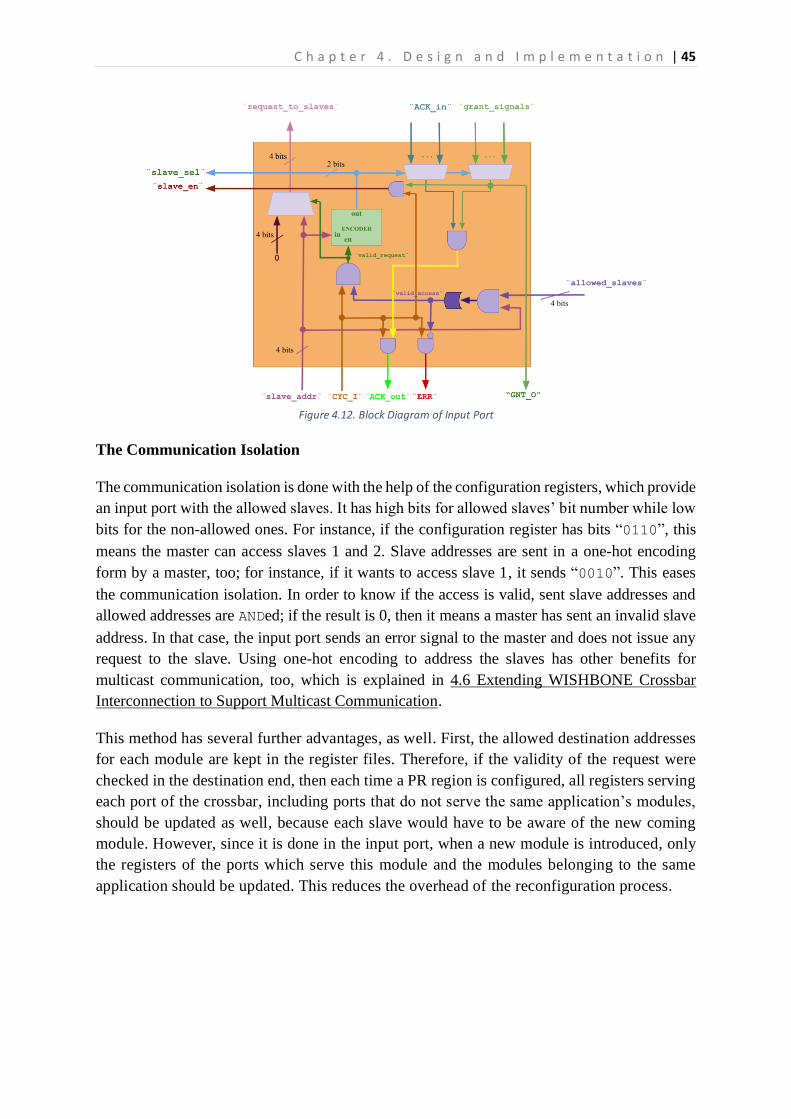
C h a p t e r 4 . D e s i g n a n d I m p l e m e n t a t i o n | 45
Figure 4.12. Block Diagram of Input Port
The Communication Isolation
The communication isolation is done with the help of the configuration registers, which provide
an input port with the allowed slaves. It has high bits for allowed slaves’ bit number while low
bits for the non-allowed ones. For instance, if the configuration register has bits “0110”, this
means the master can access slaves 1 and 2. Slave addresses are sent in a one-hot encoding
form by a master, too; for instance, if it wants to access slave 1, it sends “0010”. This eases
the communication isolation. In order to know if the access is valid, sent slave addresses and
allowed addresses are ANDed; if the result is 0, then it means a master has sent an invalid slave
address. In that case, the input port sends an error signal to the master and does not issue any
request to the slave. Using one-hot encoding to address the slaves has other benefits for
multicast communication, too, which is explained in 4.6 Extending WISHBONE Crossbar
Interconnection to Support Multicast Communication.
This method has several further advantages, as well. First, the allowed destination addresses
for each module are kept in the register files. Therefore, if the validity of the request were
checked in the destination end, then each time a PR region is configured, all registers serving
each port of the crossbar, including ports that do not serve the same application’s modules,
should be updated as well, because each slave would have to be aware of the new coming
module. However, since it is done in the input port, when a new module is introduced, only
the registers of the ports which serve this module and the modules belonging to the same
application should be updated. This reduces the overhead of the reconfiguration process.

46 | C h a p t e r 4 . D e s i g n a n d I m p l e m e n t a t i o n
Secondly, consider that a master initiates a request to a forbidden destination address, gets a
grant, and then the slave interface checks if this is a master that is supposed to be
communicated with. In this scenario, extra clock cycles would be wasted from the arbiter
logic on making a grant decision on an invalid master. Additionally, the slave would
unnecessarily waste time providing an error signal for an invalid communication while other
valid requests are pending. Thus, providing this feature in the input end reduces the possible
communication traffic on a slave end.
Evaluating a request
If the master’s request is valid, the input port forwards this request to the destination slaves.
Once the master is granted access, the input port enables the multiplexer to link the
destination slave’s data line to the master’s data input port. Moreover, it directs
acknowledgment signals of slaves to the master as long as the master has a grant.
4.5. WISHBONE Interfaces and Computation Modules
This section explains how WISHBONE interfaces and computation modules are designed
and implemented. The contributions of this part include modifying the WISHBONE features
to meet the needs of elastic resource management and, additionally, to offer a more flexible
and less costly way of implementation.
The black box block diagrams of the implemented master and slave interfaces are shown in
Figures 13 and 14, accordingly. For this work, the pipelined mode is chosen due to its high
throughput.
Figure 4.13. The Black Box View of the WISHBONE Master Interface
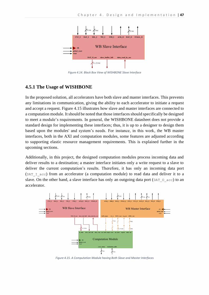
C h a p t e r 4 . D e s i g n a n d I m p l e m e n t a t i o n | 47
Figure 4.14. Black Box View of WISHBONE Slave Interface
4.5.1 The Usage of WISHBONE
In the proposed solution, all accelerators have both slave and master interfaces. This prevents
any limitations in communication, giving the ability to each accelerator to initiate a request
and accept a request. Figure 4.15 illustrates how slave and master interfaces are connected to
a computation module. It should be noted that those interfaces should specifically be designed
to meet a module’s requirements. In general, the WISHBONE datasheet does not provide a
standard design for implementing these interfaces; thus, it is up to a designer to design them
based upon the modules' and system’s needs. For instance, in this work, the WB master
interfaces, both in the AXI and computation modules, some features are adjusted according
to supporting elastic resource management requirements. This is explained further in the
upcoming sections.
Additionally, in this project, the designed computation modules process incoming data and
deliver results to a destination; a master interface initiates only a write request to a slave to
deliver the current computation’s results. Therefore, it has only an incoming data port
(DAT_I_acc) from an accelerator (a computation module) to read data and deliver it to a
slave. On the other hand, a slave interface has only an outgoing data port (DAT_O_acc) to an
accelerator.
Figure 4.15. A Computation Module having Both Slave and Master Interfaces
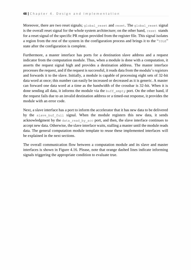
48 | C h a p t e r 4 . D e s i g n a n d I m p l e m e n t a t i o n
Moreover, there are two reset signals; global_reset and reset. The global_reset signal
is the overall reset signal for the whole system architecture; on the other hand, reset stands
for a reset signal of the specific PR region provided from the register file. This signal isolates
a region from the rest of the system in the configuration process and brings it to the “IDLE”
state after the configuration is complete.
Furthermore, a master interface has ports for a destination slave address and a request
indicator from the computation module. Thus, when a module is done with a computation, it
asserts the request signal high and provides a destination address. The master interface
processes the request, and if the request is successful, it reads data from the module’s registers
and forwards it to the slave. Initially, a module is capable of processing eight sets of 32-bit
data word at once; this number can easily be increased or decreased as it is generic. A master
can forward one data word at a time as the bandwidth of the crossbar is 32-bit. When it is
done sending all data, it informs the module via the buff_empty port. On the other hand, if
the request fails due to an invalid destination address or a timed-out response, it provides the
module with an error code.
Next, a slave interface has a port to inform the accelerator that it has new data to be delivered
by the slave_buf_full signal. When the module registers this new data, it sends
acknowledgment by the data_read_by_acc port, and then, the slave interface continues to
accept new data. Otherwise, the slave interface waits, stalling a master until the module reads
data. The general computation module template to reuse these implemented interfaces will
be explained in the next sections.
The overall communication flow between a computation module and its slave and master
interfaces is shown in Figure 4.16. Please, note that orange dashed lines indicate informing
signals triggering the appropriate condition to evaluate true.
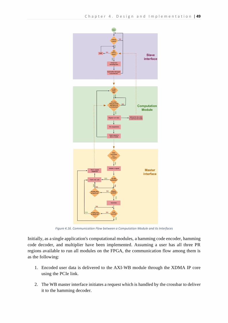
C h a p t e r 4 . D e s i g n a n d I m p l e m e n t a t i o n | 49
Figure 4.16. Communication Flow between a Computation Module and its Interfaces
Initially, as a single application's computational modules, a hamming code encoder, hamming
code decoder, and multiplier have been implemented. Assuming a user has all three PR
regions available to run all modules on the FPGA, the communication flow among them is
as the following:
1. Encoded user data is delivered to the AXI-WB module through the XDMA IP core
using the PCIe link.
2. The WB master interface initiates a request which is handled by the crossbar to deliver
it to the hamming decoder.

50 | C h a p t e r 4 . D e s i g n a n d I m p l e m e n t a t i o n
3. The hamming decoder accepts encoded data via its slave interface, processes it, and
forwards results to the multiplier via its master interface initiating a request through
the crossbar interconnection.
4. The same process happens until the final data reaches the hamming encoder after
multiplication. The encoder sends results to the WB-AXI module using its master
interface through the crossbar.
5. The WB-AXI module sends results to a user using PCIe through the XDMA IP core.
4.5.3 The Design and Implementation of the WB Master Interface
The implementation block diagram of the WB Master interface is provided in Figure 4.17. It
consists of the main control unit – the Master FSM, a couple of timeout detection FSMs, the
memory-select controller, and a multiplexer. Firstly, the multiplexer selects which data word
is going to be transferred to a slave as there are eight sets of 32-bit data coming from a
module. The selection is decided by the memory select controller, which is enabled by the
Master FSM. Secondly, the timeout FSMs; ACK Timeout FSM and GNT Timeout FSM,
detect if an acknowledgment response from a slave or a grant decision from the crossbar
takes too long. Finally, the master FSM is triggered by the request signal coming from a
computation module and manages other units to handle the request overall. This includes
processing response signals from the crossbar (GNT_I, ERR_I) or a slave (ACK_I or STALL_I),
enabling the other FSMs, and acting on their results, too.
Figure 4.17. Implementation Block Diagram of WB Master Interface
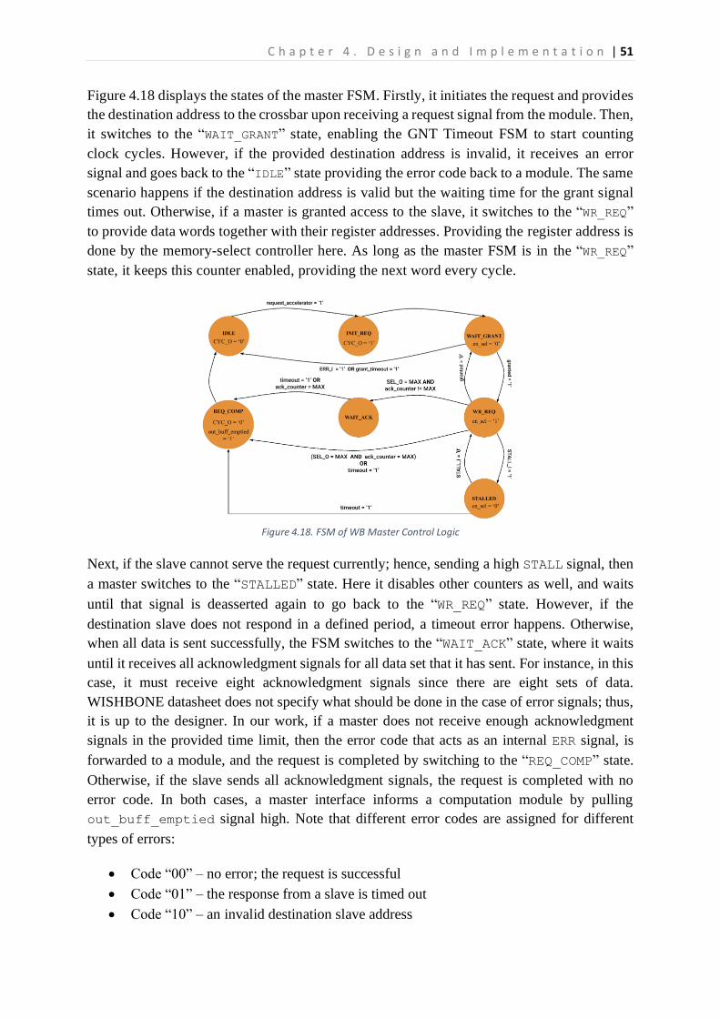
C h a p t e r 4 . D e s i g n a n d I m p l e m e n t a t i o n | 51
Figure 4.18 displays the states of the master FSM. Firstly, it initiates the request and provides
the destination address to the crossbar upon receiving a request signal from the module. Then,
it switches to the “WAIT_GRANT” state, enabling the GNT Timeout FSM to start counting
clock cycles. However, if the provided destination address is invalid, it receives an error
signal and goes back to the “IDLE” state providing the error code back to a module. The same
scenario happens if the destination address is valid but the waiting time for the grant signal
times out. Otherwise, if a master is granted access to the slave, it switches to the “WR_REQ”
to provide data words together with their register addresses. Providing the register address is
done by the memory-select controller here. As long as the master FSM is in the “WR_REQ”
state, it keeps this counter enabled, providing the next word every cycle.
Figure 4.18. FSM of WB Master Control Logic
Next, if the slave cannot serve the request currently; hence, sending a high STALL signal, then
a master switches to the “STALLED” state. Here it disables other counters as well, and waits
until that signal is deasserted again to go back to the “WR_REQ” state. However, if the
destination slave does not respond in a defined period, a timeout error happens. Otherwise,
when all data is sent successfully, the FSM switches to the “WAIT_ACK” state, where it waits
until it receives all acknowledgment signals for all data set that it has sent. For instance, in this
case, it must receive eight acknowledgment signals since there are eight sets of data.
WISHBONE datasheet does not specify what should be done in the case of error signals; thus,
it is up to the designer. In our work, if a master does not receive enough acknowledgment
signals in the provided time limit, then the error code that acts as an internal ERR signal, is
forwarded to a module, and the request is completed by switching to the “REQ_COMP” state.
Otherwise, if the slave sends all acknowledgment signals, the request is completed with no
error code. In both cases, a master interface informs a computation module by pulling
out_buff_emptied signal high. Note that different error codes are assigned for different
types of errors:
• Code “00” – no error; the request is successful
• Code “01” – the response from a slave is timed out
• Code “10” – an invalid destination slave address
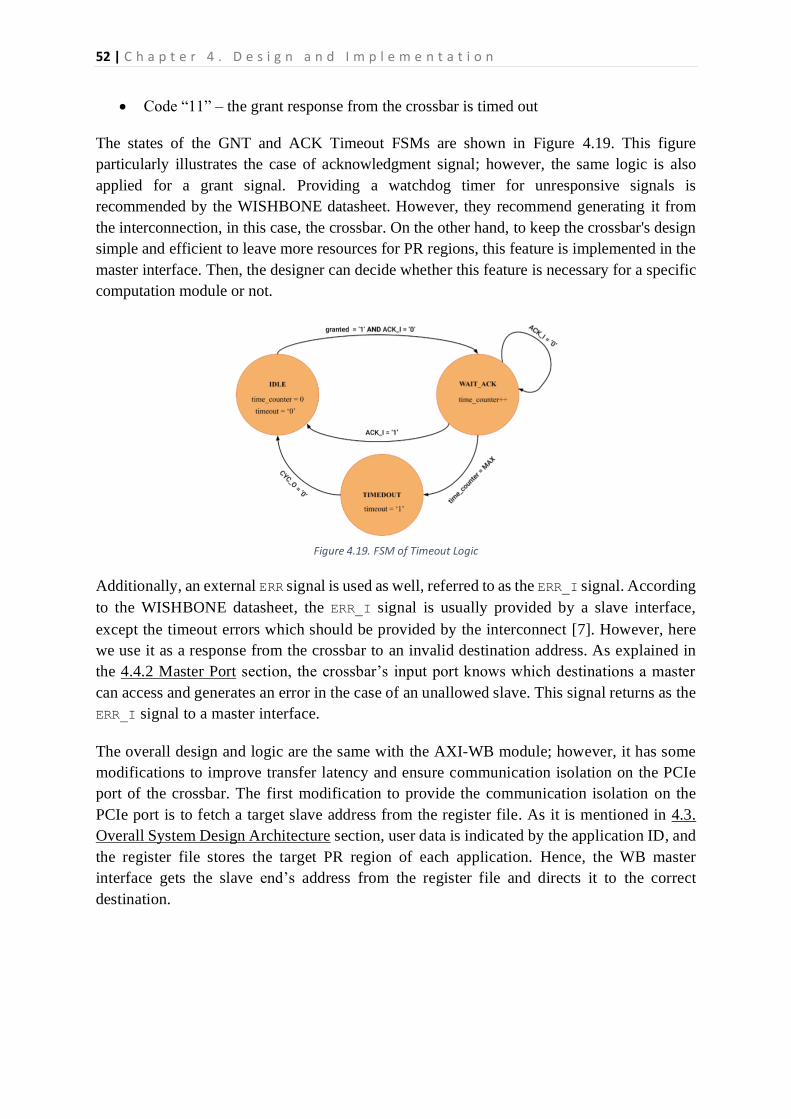
52 | C h a p t e r 4 . D e s i g n a n d I m p l e m e n t a t i o n
• Code “11” – the grant response from the crossbar is timed out
The states of the GNT and ACK Timeout FSMs are shown in Figure 4.19. This figure
particularly illustrates the case of acknowledgment signal; however, the same logic is also
applied for a grant signal. Providing a watchdog timer for unresponsive signals is
recommended by the WISHBONE datasheet. However, they recommend generating it from
the interconnection, in this case, the crossbar. On the other hand, to keep the crossbar's design
simple and efficient to leave more resources for PR regions, this feature is implemented in the
master interface. Then, the designer can decide whether this feature is necessary for a specific
computation module or not.
Figure 4.19. FSM of Timeout Logic
Additionally, an external ERR signal is used as well, referred to as the ERR_I signal. According
to the WISHBONE datasheet, the ERR_I signal is usually provided by a slave interface,
except the timeout errors which should be provided by the interconnect [7]. However, here
we use it as a response from the crossbar to an invalid destination address. As explained in
the 4.4.2 Master Port section, the crossbar’s input port knows which destinations a master
can access and generates an error in the case of an unallowed slave. This signal returns as the
ERR_I signal to a master interface.
The overall design and logic are the same with the AXI-WB module; however, it has some
modifications to improve transfer latency and ensure communication isolation on the PCIe
port of the crossbar. The first modification to provide the communication isolation on the
PCIe port is to fetch a target slave address from the register file. As it is mentioned in 4.3.
Overall System Design Architecture section, user data is indicated by the application ID, and
the register file stores the target PR region of each application. Hence, the WB master
interface gets the slave end’s address from the register file and directs it to the correct
destination.
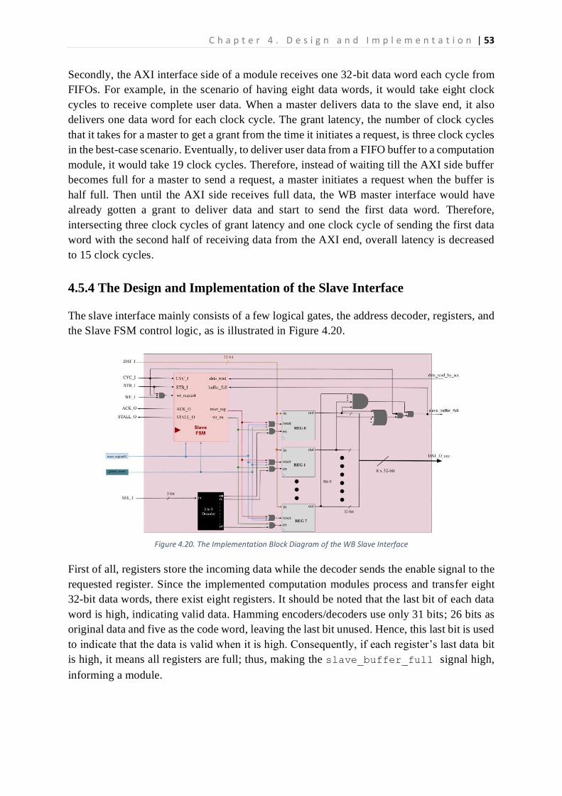
C h a p t e r 4 . D e s i g n a n d I m p l e m e n t a t i o n | 53
Secondly, the AXI interface side of a module receives one 32-bit data word each cycle from
FIFOs. For example, in the scenario of having eight data words, it would take eight clock
cycles to receive complete user data. When a master delivers data to the slave end, it also
delivers one data word for each clock cycle. The grant latency, the number of clock cycles
that it takes for a master to get a grant from the time it initiates a request, is three clock cycles
in the best-case scenario. Eventually, to deliver user data from a FIFO buffer to a computation
module, it would take 19 clock cycles. Therefore, instead of waiting till the AXI side buffer
becomes full for a master to send a request, a master initiates a request when the buffer is
half full. Then until the AXI side receives full data, the WB master interface would have
already gotten a grant to deliver data and start to send the first data word. Therefore,
intersecting three clock cycles of grant latency and one clock cycle of sending the first data
word with the second half of receiving data from the AXI end, overall latency is decreased
to 15 clock cycles.
4.5.4 The Design and Implementation of the Slave Interface
The slave interface mainly consists of a few logical gates, the address decoder, registers, and
the Slave FSM control logic, as is illustrated in Figure 4.20.
Figure 4.20. The Implementation Block Diagram of the WB Slave Interface
First of all, registers store the incoming data while the decoder sends the enable signal to the
requested register. Since the implemented computation modules process and transfer eight
32-bit data words, there exist eight registers. It should be noted that the last bit of each data
word is high, indicating valid data. Hamming encoders/decoders use only 31 bits; 26 bits as
original data and five as the code word, leaving the last bit unused. Hence, this last bit is used
to indicate that the data is valid when it is high. Consequently, if each register’s last data bit
is high, it means all registers are full; thus, making the slave_buffer_full signal high,
informing a module.
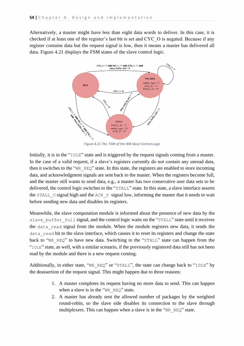
54 | C h a p t e r 4 . D e s i g n a n d I m p l e m e n t a t i o n
Alternatively, a master might have less than eight data words to deliver. In this case, it is
checked if at least one of the register’s last bit is set and CYC_O is negated. Because if any
register contains data but the request signal is low, then it means a master has delivered all
data. Figure 4.21 displays the FSM states of the slave control logic.
Figure 4.21.The FSM of the WB Slave Control Logic
Initially, it is in the “IDLE” state and is triggered by the request signals coming from a master.
In the case of a valid request, if a slave’s registers currently do not contain any unread data,
then it switches to the “WR_REQ” state. In this state, the registers are enabled to store incoming
data, and acknowledgment signals are sent back to the master. When the registers become full,
and the master still wants to send data, e.g., a master has two consecutive user data sets to be
delivered, the control logic switches to the “STALL” state. In this state, a slave interface asserts
the STALL_O signal high and the ACK_O signal low, informing the master that it needs to wait
before sending new data and disables its registers.
Meanwhile, the slave computation module is informed about the presence of new data by the
slave_buffer_full signal, and the control logic waits on the “STALL” state until it receives
the data_read signal from the module. When the module registers new data, it sends the
data_read bit to the slave interface, which causes it to reset its registers and change the state
back to “WR_REQ” to have new data. Switching to the “STALL” state can happen from the
“IDLE” state, as well, with a similar scenario, if the previously registered data still has not been
read by the module and there is a new request coming.
Additionally, in either state, “WR_REQ” or “STALL”, the state can change back to “IDLE” by
the deassertion of the request signal. This might happen due to three reasons:
1. A master completes its request having no more data to send. This can happen
when a slave is in the “WR_REQ” state.
2. A master has already sent the allowed number of packages by the weighted
round-robin, so the slave side disables its connection to the slave through
multiplexers. This can happen when a slave is in the “WR_REQ” state.
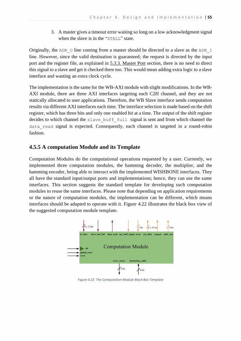
C h a p t e r 4 . D e s i g n a n d I m p l e m e n t a t i o n | 55
3. A master gives a timeout error waiting so long on a low acknowledgment signal
when the slave is in the “STALL” state.
Originally, the ADR_O line coming from a master should be directed to a slave as the ADR_I
line. However, since the valid destination is guaranteed; the request is directed by the input
port and the register file, as explained in 5.3.3. Master Port section, there is no need to direct
this signal to a slave and get it checked there too. This would mean adding extra logic to a slave
interface and wasting an extra clock cycle.
The implementation is the same for the WB-AXI module with slight modifications. In the WB-
AXI module, there are three AXI interfaces targeting each C2H channel, and they are not
statically allocated to user applications. Therefore, the WB Slave interface sends computation
results via different AXI interfaces each time. The interface selection is made based on the shift
register, which has three bits and only one enabled bit at a time. The output of the shift register
decides to which channel the slave_buff_full signal is sent and from which channel the
data_read signal is expected. Consequently, each channel is targeted in a round-robin
fashion.
4.5.5 A computation Module and its Template
Computation Modules do the computational operations requested by a user. Currently, we
implemented three computation modules, the hamming decoder, the multiplier, and the
hamming encoder, being able to interact with the implemented WISHBONE interfaces. They
all have the standard input/output ports and implementations; hence, they can use the same
interfaces. This section suggests the standard template for developing such computation
modules to reuse the same interfaces. Please note that depending on application requirements
or the nature of computation modules, the implementation can be different, which means
interfaces should be adapted to operate with it. Figure 4.22 illustrates the black box view of
the suggested computation module template.
Figure 4.22. The Computation Module Black Box Template
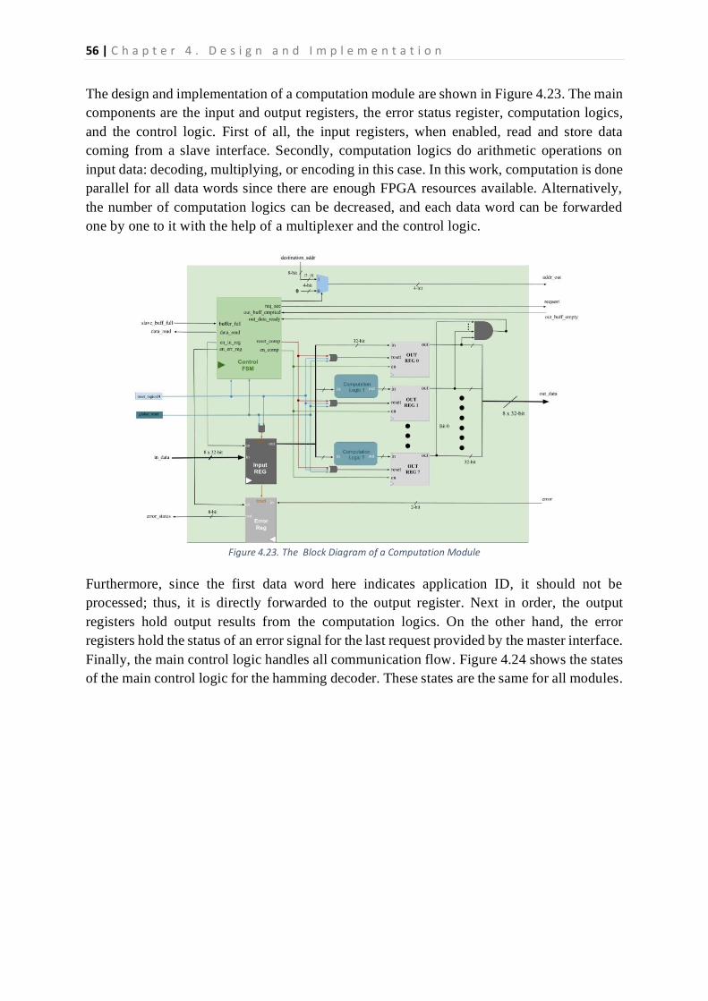
56 | C h a p t e r 4 . D e s i g n a n d I m p l e m e n t a t i o n
The design and implementation of a computation module are shown in Figure 4.23. The main
components are the input and output registers, the error status register, computation logics,
and the control logic. First of all, the input registers, when enabled, read and store data
coming from a slave interface. Secondly, computation logics do arithmetic operations on
input data: decoding, multiplying, or encoding in this case. In this work, computation is done
parallel for all data words since there are enough FPGA resources available. Alternatively,
the number of computation logics can be decreased, and each data word can be forwarded
one by one to it with the help of a multiplexer and the control logic.
Figure 4.23. The Block Diagram of a Computation Module
Furthermore, since the first data word here indicates application ID, it should not be
processed; thus, it is directly forwarded to the output register. Next in order, the output
registers hold output results from the computation logics. On the other hand, the error
registers hold the status of an error signal for the last request provided by the master interface.
Finally, the main control logic handles all communication flow. Figure 4.24 shows the states
of the main control logic for the hamming decoder. These states are the same for all modules.
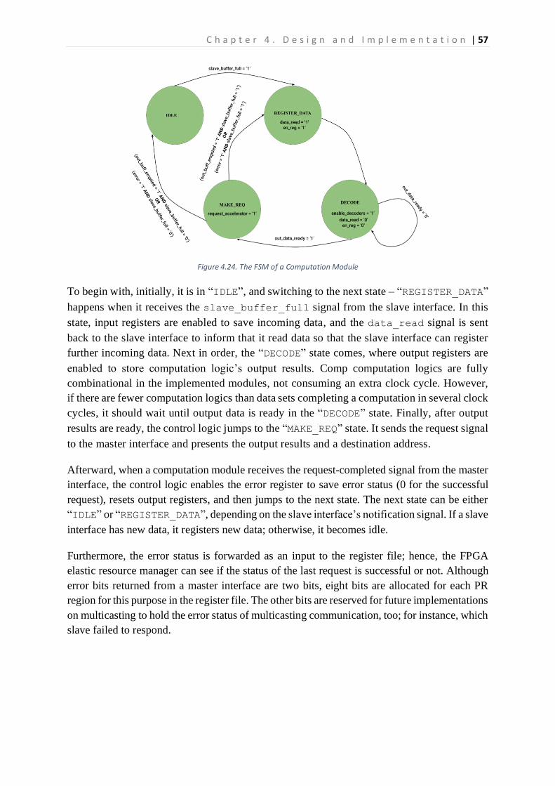
C h a p t e r 4 . D e s i g n a n d I m p l e m e n t a t i o n | 57
Figure 4.24. The FSM of a Computation Module
To begin with, initially, it is in “IDLE”, and switching to the next state – “REGISTER_DATA”
happens when it receives the slave_buffer_full signal from the slave interface. In this
state, input registers are enabled to save incoming data, and the data_read signal is sent
back to the slave interface to inform that it read data so that the slave interface can register
further incoming data. Next in order, the “DECODE” state comes, where output registers are
enabled to store computation logic’s output results. Comp computation logics are fully
combinational in the implemented modules, not consuming an extra clock cycle. However,
if there are fewer computation logics than data sets completing a computation in several clock
cycles, it should wait until output data is ready in the “DECODE” state. Finally, after output
results are ready, the control logic jumps to the “MAKE_REQ” state. It sends the request signal
to the master interface and presents the output results and a destination address.
Afterward, when a computation module receives the request-completed signal from the master
interface, the control logic enables the error register to save error status (0 for the successful
request), resets output registers, and then jumps to the next state. The next state can be either
“IDLE” or “REGISTER_DATA”, depending on the slave interface’s notification signal. If a slave
interface has new data, it registers new data; otherwise, it becomes idle.
Furthermore, the error status is forwarded as an input to the register file; hence, the FPGA
elastic resource manager can see if the status of the last request is successful or not. Although
error bits returned from a master interface are two bits, eight bits are allocated for each PR
region for this purpose in the register file. The other bits are reserved for future implementations
on multicasting to hold the error status of multicasting communication, too; for instance, which
slave failed to respond.
58 | C h a p t e r 4 . D e s i g n a n d I m p l e m e n t a t i o n
4.6. Extending the WISHBONE Crossbar Interconnection to
Support Multicast Communication
This section proposes the solution in order to support multicast communication in the
WISHBONE Crossbar Interconnection. The novelty here consists of improving the
WISHBONE master interface and the crossbar interconnection to support sending data to
different slaves simultaneously while still ensuring the communication isolation. The multicast
communication pattern can be needed when a computation module sends its results to multiple
computation modules to get different results from each. For instance, a picture file can be sent
to two computation modules where one module identifies people in the picture, and the other
filters vehicles present there. In this case, instead of generating two different requests for each
module, it is more efficient if data can be sent to both simultaneously.
The main challenges to consider are providing the communication isolation and managing
response signals – GNT, ACK, and STALL coming from different slave sides simultaneously.
Our solution of multicasting has the following benefits:
• This is the first solution done for multicast communication using the WISHBONE
Crossbar Interconnection.
• Addressing multiple slaves is done in a much simpler manner reducing the multicast
overhead.
• The slave interface logic remains unchanged and unrelated slaves are not disturbed,
leading to a less costly slave interface.
• Meanwhile, the communication isolation is still achieved.
Figure 4.25 illustrates the proposed solution for handling multicast communication. Since the
master port of the crossbar generally provides the signals mentioned above and the
communication isolation, the main modifications for multicast purposes should be done there,
too. Please, note that the figure illustrates the main design considerations. Enabling data signals
coming from slaves can be done in the same way as shown in Figure 4.11.
Communication Isolation
First of all, the communication isolation is provided with the help of the register file. Here
requesting slaves by bit-addressing simplifies requesting different slaves. To illustrate, as
mentioned in the 4.4.2 Master Port section, addressing slaves is done by one-hot encoding;
here, the same logic applies. However, instead of only 1 bit, several bits can be high, each bit
representing one slave. For instance, if the ADR_O signal is “0111”, a master wants to send
data to the slaves connected to ports 0, 1, and 2. On the other hand, the register file stores the
allowed slaves for a master. Consider, it is “0110”, meaning a master is allowed to
communicate with slaves 1 and 3. Then, ADR_O and allowed_slaves are ANDed, resulting
in “0110”, and the result is forwarded as request bits; thus, port 0 is safe while the request is
sent only to valid slaves. On the other hand, if a master’s all destinations are invalid, the
valid_access signal is evaluated as false, and ERR_I is returned to the master.
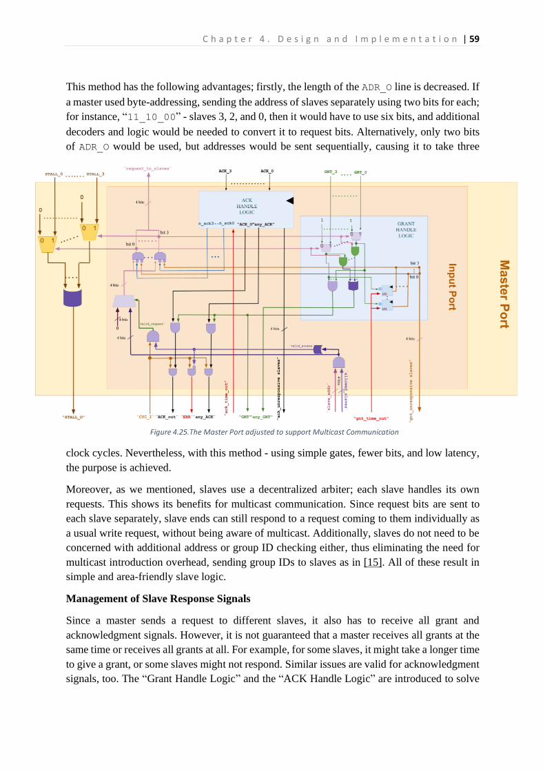
C h a p t e r 4 . D e s i g n a n d I m p l e m e n t a t i o n | 59
This method has the following advantages; firstly, the length of the ADR_O line is decreased. If
a master used byte-addressing, sending the address of slaves separately using two bits for each;
for instance, “11_10_00” - slaves 3, 2, and 0, then it would have to use six bits, and additional
decoders and logic would be needed to convert it to request bits. Alternatively, only two bits
of ADR_O would be used, but addresses would be sent sequentially, causing it to take three
clock cycles. Nevertheless, with this method - using simple gates, fewer bits, and low latency,
the purpose is achieved.
Moreover, as we mentioned, slaves use a decentralized arbiter; each slave handles its own
requests. This shows its benefits for multicast communication. Since request bits are sent to
each slave separately, slave ends can still respond to a request coming to them individually as
a usual write request, without being aware of multicast. Additionally, slaves do not need to be
concerned with additional address or group ID checking either, thus eliminating the need for
multicast introduction overhead, sending group IDs to slaves as in [15]. All of these result in
simple and area-friendly slave logic.
Management of Slave Response Signals
Since a master sends a request to different slaves, it also has to receive all grant and
acknowledgment signals. However, it is not guaranteed that a master receives all grants at the
same time or receives all grants at all. For example, for some slaves, it might take a longer time
to give a grant, or some slaves might not respond. Similar issues are valid for acknowledgment
signals, too. The “Grant Handle Logic” and the “ACK Handle Logic” are introduced to solve
Figure 4.25.The Master Port adjusted to support Multicast Communication
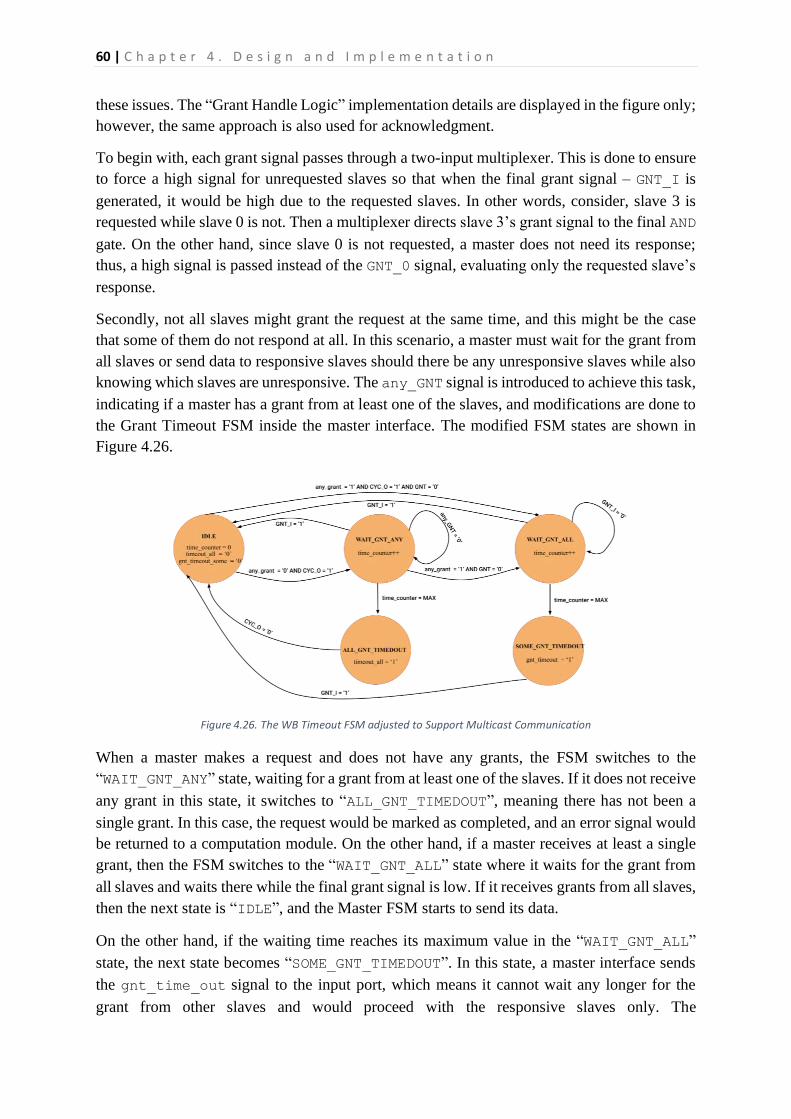
60 | C h a p t e r 4 . D e s i g n a n d I m p l e m e n t a t i o n
these issues. The “Grant Handle Logic” implementation details are displayed in the figure only;
however, the same approach is also used for acknowledgment.
To begin with, each grant signal passes through a two-input multiplexer. This is done to ensure
to force a high signal for unrequested slaves so that when the final grant signal – GNT_I is
generated, it would be high due to the requested slaves. In other words, consider, slave 3 is
requested while slave 0 is not. Then a multiplexer directs slave 3’s grant signal to the final AND
gate. On the other hand, since slave 0 is not requested, a master does not need its response;
thus, a high signal is passed instead of the GNT_0 signal, evaluating only the requested slave’s
response.
Secondly, not all slaves might grant the request at the same time, and this might be the case
that some of them do not respond at all. In this scenario, a master must wait for the grant from
all slaves or send data to responsive slaves should there be any unresponsive slaves while also
knowing which slaves are unresponsive. The any_GNT signal is introduced to achieve this task,
indicating if a master has a grant from at least one of the slaves, and modifications are done to
the Grant Timeout FSM inside the master interface. The modified FSM states are shown in
Figure 4.26.
Figure 4.26. The WB Timeout FSM adjusted to Support Multicast Communication
When a master makes a request and does not have any grants, the FSM switches to the
“WAIT_GNT_ANY” state, waiting for a grant from at least one of the slaves. If it does not receive
any grant in this state, it switches to “ALL_GNT_TIMEDOUT”, meaning there has not been a
single grant. In this case, the request would be marked as completed, and an error signal would
be returned to a computation module. On the other hand, if a master receives at least a single
grant, then the FSM switches to the “WAIT_GNT_ALL” state where it waits for the grant from
all slaves and waits there while the final grant signal is low. If it receives grants from all slaves,
then the next state is “IDLE”, and the Master FSM starts to send its data.
On the other hand, if the waiting time reaches its maximum value in the “WAIT_GNT_ALL”
state, the next state becomes “SOME_GNT_TIMEDOUT”. In this state, a master interface sends
the gnt_time_out signal to the input port, which means it cannot wait any longer for the
grant from other slaves and would proceed with the responsive slaves only. The
C h a p t e r 4 . D e s i g n a n d I m p l e m e n t a t i o n | 61
gnt_time_out signal enables registers inside the Grant Handle Logic to negate incoming
grant signals from slaves. Low grant signals are registered high, indicating which slave did not
respond to the request. For instance, if slaves 0 and 3 are requested, slave 3 is granted, but slave
0 is not, then the output of the registers inside becomes “0001”. This is directed as
unresponsive slave addresses to a master interface.
Moreover, outputs of the Grant Handle Logic’s registers are negated and ANDed with the output
request bits, causing to cancel request signals to the unresponsive slaves and making
multiplexer select signals for those slaves 0 accordingly, thus, proceeding with only the
responsive slaves. Since the request to the timed-out slave is canceled, GNT_O is evaluated true,
causing the timeout FSM to switch to the “IDLE” state. Next in order, the master interface
registers the unresponsive slave IDs and forwards them to the computation module with the
error code so that the status can be registered in the register file. For example, if slave 0 did not
give a grant, a master would forward “0001_11” – “slave0_grant-timeout”. Afterward, a
master interface starts to send data to granted slaves.
The same approach applies to ACK Handle Logic; however, there are some additional issues
and assumptions to consider here. First of all, since a master waits for all grant signals before
sending data, it means all destined slaves become available at the same time; thus, all
acknowledgment signals come simultaneously too, causing the ACK_O signal to be evaluated to
true. On the other hand, in this case, there might occur two scenarios causing low
acknowledgment signals from some slaves. First, some slaves might have less buffer space
than others, causing STALL and a low acknowledgment signal. If at least one of the slaves
asserts the STALL signal, then the master FSM switches to the “STALLED” state as shown in
Figure 4.18 and hence, waiting without sending data to other slaves. Meanwhile, the
acknowledgment timeout FSM, which has the same states and logic as in Figure 4.19, starts to
keep track, as well. If the slave who has sent STALL does not respond to in defined time limit,
the ack_time_out signal is sent to the input port, causing to cancel the request to the timed-
out slave, registering its address from ack_unresponsive_slaves, and again proceeding
with the responsive slaves.
The other scenario where ACK_O might be evaluated as false is when a slave might be stuck
and does not operate. In this case, the same procedures apply again, and a master proceeds with
responsive slaves. Additionally, if none of the slaves sends an acknowledgment signal, the
request is marked as complete with an error status.
Furthermore, STALL_I signals pass through two-input multiplexers, causing to consider only
requested slaves’ signals. As mentioned, when a single slave asserts a high STALL signal, then
a master must wait for it. Therefore, the final STALL_O output directed to a master interface
is evaluated with the OR gate.
Finally, since multicast communication sends data to multiple slaves, it is unnecessary to
modify how to handle DAT_I signals from slaves shown in Figure 4.11, as they are not used.
Thus, this part of the input port can stay the same.
Chapter 5. Design Verification and Results
5.1. Design Verification
All self-developed modules were tested and verified using testbenches and simulation before
being integrated. The final system architecture was tested in simulation, as well as in the
FPGA device.
5.1.1 Verification in the Simulation environment
The simulation environment is provided by Xilinx Vivado Tool 2018.3. The input signals to
hardware modules were randomly generated using functions in testbenches.
The WISHBONE Crossbar
The Crossbar’s submodules: the WRR, input/output ports, etc., were tested separately first.
Then they were integrated together and verified in two steps. In the first step, only a single
port was tested; in the second step, all four ports were tested together.
The WB interfaces and computation modules
Firstly, each computation module’s functionality was tested, as well as master and slave
interfaces. Then, the encoder and decoders were connected point-to-point using interfaces.
Their inputs and outputs were compared to check the overall flow between computation
modules and bus interfaces.
The AXI-WB and WB-AXI modules
To verify these modules' functionalities, they were connected in a point-to-point fashion.
Moreover, they were also tested separately with AXI-ST FIFO modules provided by Xilinx.
The Integrated system
The modules were integrated and verified step-by-step. First, WB computation modules were
connected to the crossbar interconnection, and the AXI/WB module sides together with
FIFOs were simulated separately using randomized input signals. Then, AXI/WB modules
and the register file were added to the crossbar system and tested. After the results were
verified, the XDMA IP core was added to the system architecture, and the resulting design
was tested on the KCU1500 board.
C h a p t e r 5 . D e s i g n V e r i f i c a t i o n a n d R e s u l t s | 63
5.1.2 Verification in the FPGA device
For verification in the actual device, different scenarios were followed, and results were
verified referring to the register file in addition to input/output files. A couple of scenarios are
provided in the 5.2 Results section to demonstrate the dynamic resource allocation and
communication isolation features.
5.2. Results
In this section, the results of the final system architecture are assessed. This includes
summarizing system features and demonstrating the important ones on the FPGA device.
Additionally, the area usage and the power consumption of the system are presented, as well.
5.2.1 The System Features
The features of the implemented system architecture are summarized as below:
1. The configurable four-port WISHBONE Crossbar communication interconnection which:
• enables to increase/decrease the number of resources allocated to an application
• allows dynamic bandwidth allocation for different applications
• provides the communication isolation
2. The XDMA IP Core with 6 AXI-ST channels to exchange user data
3. Three different statically implemented computation modules; the multiplier, the hamming
encoder, and the hamming decoder, together with the WISHBONE master and slave
interfaces
4. The AXI-WB and WB-AXI modules
5. The register file:
• to serve computation modules and the crossbar with configuration data
• to save status data from computations and the AXI-WB and WB-AXI modules.
5.2.2 Demonstration of Some Features
This section briefly displays the important features of the developed system on the KCU1500
board. In all those experiments, the PCIe link is connected to crossbar port 0, the multiplier to
port 1, the encoder to port 2, and the decoder to port 3.
Elastic Resource Allocation and Dynamic Bandwidth
To show dynamic elastic resource allocation, we did an experiment to show how elasticity
improves the application's execution time. For this purpose, 16 KB data was sent to be
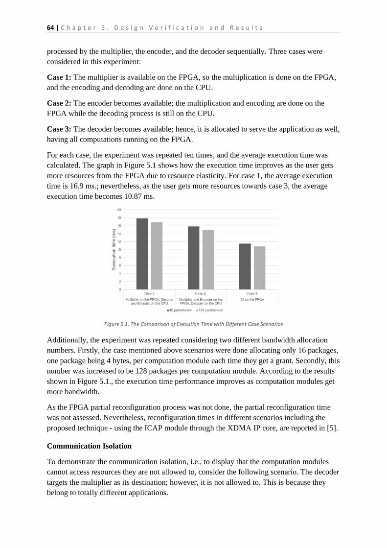
64 | C h a p t e r 5 . D e s i g n V e r i f i c a t i o n a n d R e s u l t s
processed by the multiplier, the encoder, and the decoder sequentially. Three cases were
considered in this experiment:
Case 1: The multiplier is available on the FPGA, so the multiplication is done on the FPGA,
and the encoding and decoding are done on the CPU.
Case 2: The encoder becomes available; the multiplication and encoding are done on the
FPGA while the decoding process is still on the CPU.
Case 3: The decoder becomes available; hence, it is allocated to serve the application as well,
having all computations running on the FPGA.
For each case, the experiment was repeated ten times, and the average execution time was
calculated. The graph in Figure 5.1 shows how the execution time improves as the user gets
more resources from the FPGA due to resource elasticity. For case 1, the average execution
time is 16.9 ms.; nevertheless, as the user gets more resources towards case 3, the average
execution time becomes 10.87 ms.
Figure 5.1. The Comparison of Execution Time with Different Case Scenarios
Additionally, the experiment was repeated considering two different bandwidth allocation
numbers. Firstly, the case mentioned above scenarios were done allocating only 16 packages,
one package being 4 bytes, per computation module each time they get a grant. Secondly, this
number was increased to be 128 packages per computation module. According to the results
shown in Figure 5.1., the execution time performance improves as computation modules get
more bandwidth.
As the FPGA partial reconfiguration process was not done, the partial reconfiguration time
was not assessed. Nevertheless, reconfiguration times in different scenarios including the
proposed technique - using the ICAP module through the XDMA IP core, are reported in [5].
Communication Isolation
To demonstrate the communication isolation, i.e., to display that the computation modules
cannot access resources they are not allowed to, consider the following scenario. The decoder
targets the multiplier as its destination; however, it is not allowed to. This is because they
belong to totally different applications.

C h a p t e r 5 . D e s i g n V e r i f i c a t i o n a n d R e s u l t s | 65
In Figure 5.5, the decoder’s allowed slave address is shown in a green box. It can access slave
number 0 only. However, by the first command, the decoder’s destination address is
configured to be slave connected to port 1, which is the multiplier. Then, the data is sent to
the FPGA device to be computed.
Figure 5.2. Communication Isolation Demonstration
After sending data, the error status can be assessed from the register file, shown in the orange
box. The figure shows that the error status for computation module number 3 has been
changed to “02,” which is the invalid address error code. At the same time, when data is
read back by the last command shown in Figure 5.5, it throws an error since there is no data
to read back. This is because the decoder dropped the data when the error occurred. As a
result, when the module tried to access an invalid address, it was prevented, and the error
status was registered. Thus, communication isolation was achieved.
5.2.3 Communication Overhead
The communication overhead here refers to “time-to-grant” – the number of clock cycles
from when a computation module initiates a request to when the master interface starts to
send the first data. The best-case time-to-grant is four clock cycles where the slave does not
serve any request currently, and a master gets the grant immediately. It takes one clock cycle
for a module’s request to reach the master interface, and the master interface initiates a
request in the next clock cycle. On the other hand, the slave side takes two clock cycles to
grant the request and enable the slave interface. As a result, if a computation module has
eight packages to deliver, then it takes 13 clock cycles in the best case to complete the
request. Here, the last clock cycle is used to register the error status of the transaction.
On the other hand, the worst-case time-to-grant occurs when all three computation modules
target the 4th one simultaneously. The master who would be served the last would have to
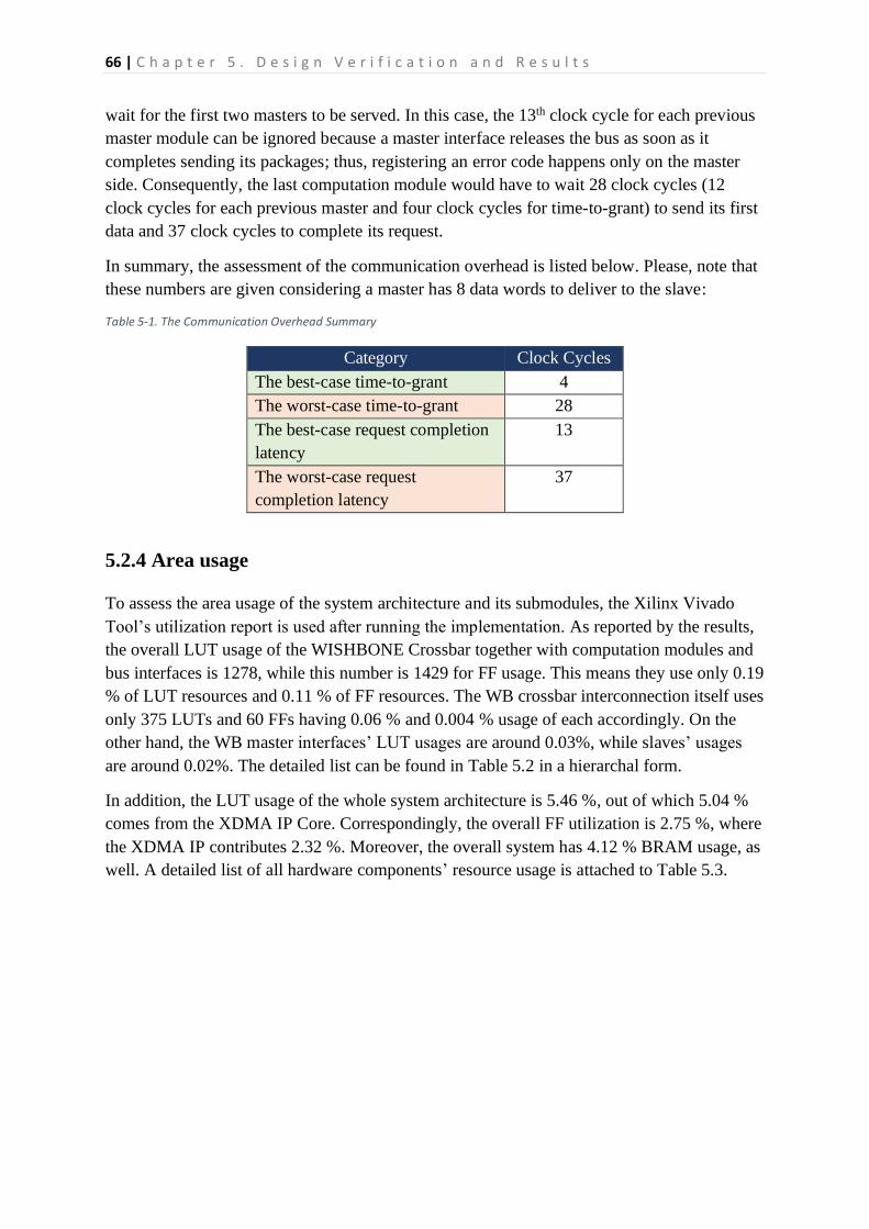
66 | C h a p t e r 5 . D e s i g n V e r i f i c a t i o n a n d R e s u l t s
wait for the first two masters to be served. In this case, the 13th clock cycle for each previous
master module can be ignored because a master interface releases the bus as soon as it
completes sending its packages; thus, registering an error code happens only on the master
side. Consequently, the last computation module would have to wait 28 clock cycles (12
clock cycles for each previous master and four clock cycles for time-to-grant) to send its first
data and 37 clock cycles to complete its request.
In summary, the assessment of the communication overhead is listed below. Please, note that
these numbers are given considering a master has 8 data words to deliver to the slave:
Table 5-1. The Communication Overhead Summary
Category Clock Cycles
The best-case time-to-grant 4
The worst-case time-to-grant 28
The best-case request completion
latency
13
The worst-case request
completion latency
37
5.2.4 Area usage
To assess the area usage of the system architecture and its submodules, the Xilinx Vivado
Tool’s utilization report is used after running the implementation. As reported by the results,
the overall LUT usage of the WISHBONE Crossbar together with computation modules and
bus interfaces is 1278, while this number is 1429 for FF usage. This means they use only 0.19
% of LUT resources and 0.11 % of FF resources. The WB crossbar interconnection itself uses
only 375 LUTs and 60 FFs having 0.06 % and 0.004 % usage of each accordingly. On the
other hand, the WB master interfaces’ LUT usages are around 0.03%, while slaves’ usages
are around 0.02%. The detailed list can be found in Table 5.2 in a hierarchal form.
In addition, the LUT usage of the whole system architecture is 5.46 %, out of which 5.04 %
comes from the XDMA IP Core. Correspondingly, the overall FF utilization is 2.75 %, where
the XDMA IP contributes 2.32 %. Moreover, the overall system has 4.12 % BRAM usage, as
well. A detailed list of all hardware components’ resource usage is attached to Table 5.3.
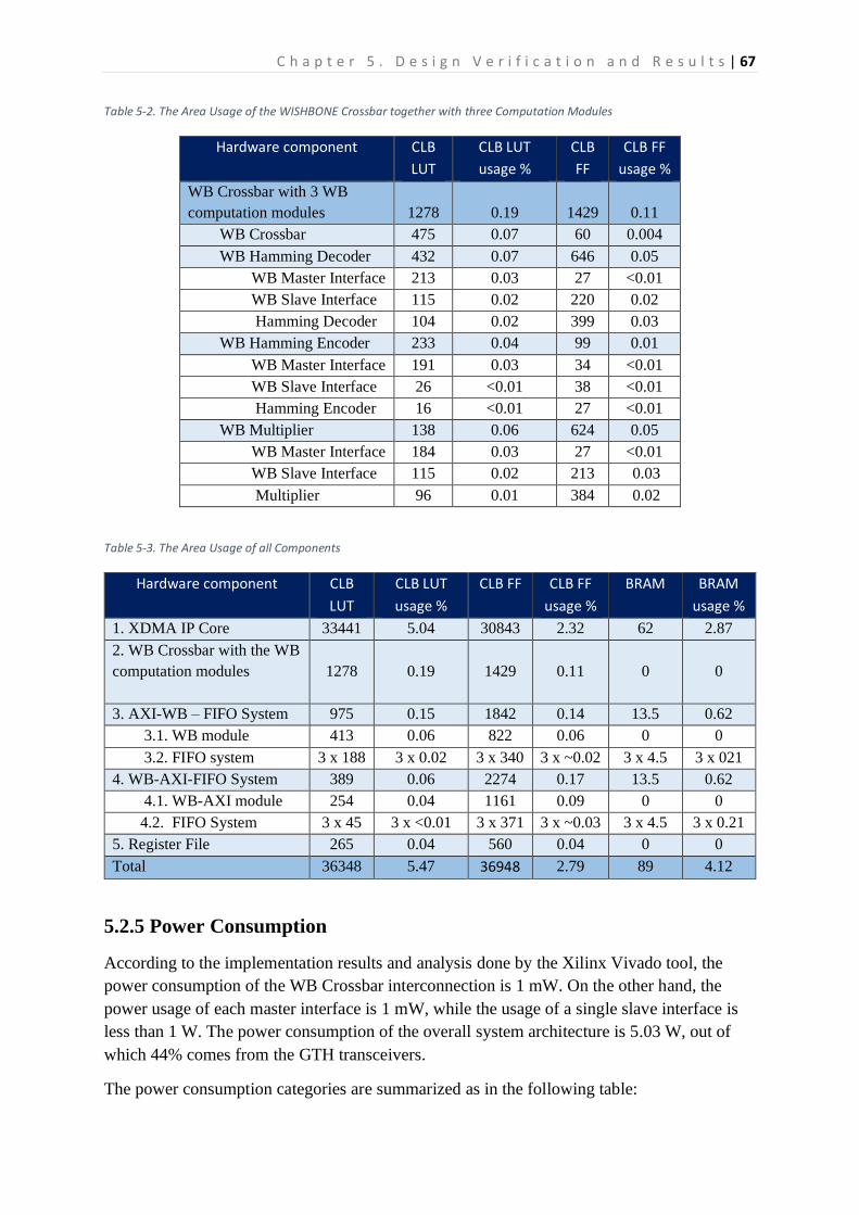
C h a p t e r 5 . D e s i g n V e r i f i c a t i o n a n d R e s u l t s | 67
Table 5-2. The Area Usage of the WISHBONE Crossbar together with three Computation Modules
Hardware component CLB
LUT
CLB LUT
usage %
CLB
FF
CLB FF
usage %
WB Crossbar with 3 WB
computation modules
1278
0.19
1429
0.11
WB Crossbar 475 0.07 60 0.004
WB Hamming Decoder 432 0.07 646 0.05
WB Master Interface 213 0.03 27 <0.01
WB Slave Interface 115 0.02 220 0.02
Hamming Decoder 104 0.02 399 0.03
WB Hamming Encoder 233 0.04 99 0.01
WB Master Interface 191 0.03 34 <0.01
WB Slave Interface 26 <0.01 38 <0.01
Hamming Encoder 16 <0.01 27 <0.01
WB Multiplier 138 0.06 624 0.05
WB Master Interface 184 0.03 27 <0.01
WB Slave Interface 115 0.02 213 0.03
Multiplier 96 0.01 384 0.02
Table 5-3. The Area Usage of all Components
Hardware component CLB
LUT
CLB LUT
usage %
CLB FF CLB FF
usage %
BRAM BRAM
usage %
1. XDMA IP Core 33441 5.04 30843 2.32 62 2.87
2. WB Crossbar with the WB
computation modules
1278
0.19
1429
0.11
0
0
3. AXI-WB – FIFO System 975 0.15 1842 0.14 13.5 0.62
3.1. WB module 413 0.06 822 0.06 0 0
3.2. FIFO system 3 x 188 3 x 0.02 3 x 340 3 x ~0.02 3 x 4.5 3 x 021
4. WB-AXI-FIFO System 389 0.06 2274 0.17 13.5 0.62
4.1. WB-AXI module 254 0.04 1161 0.09 0 0
4.2. FIFO System 3 x 45 3 x <0.01 3 x 371 3 x ~0.03 3 x 4.5 3 x 0.21
5. Register File 265 0.04 560 0.04 0 0
Total 36348 5.47 36948 2.79 89 4.12
5.2.5 Power Consumption
According to the implementation results and analysis done by the Xilinx Vivado tool, the
power consumption of the WB Crossbar interconnection is 1 mW. On the other hand, the
power usage of each master interface is 1 mW, while the usage of a single slave interface is
less than 1 W. The power consumption of the overall system architecture is 5.03 W, out of
which 44% comes from the GTH transceivers.
The power consumption categories are summarized as in the following table:

68 | C h a p t e r 5 . D e s i g n V e r i f i c a t i o n a n d R e s u l t s
Table 5-4. The Power Usage by Categories
Category Power Consumption
(W)
GTH 2.215
Hard IP 0.298
Dynamic Power 1.139
Device Static Power 1.379
Total 5.031
The power consumption of the individual hardware modules is listed as below:
Table 5-5. The Power Usage by Hardware Components
Hardware Component Power Consumption
(W)
1. XDMA IP Core 3.583
2. WISHBONE Crossbar 0.001
3. WB Hamming Encoder 0.001
3.1. Hamming Encoder <0.01
3.2. WB Master Interface 0.001
3.3. WB Slave Interface <0.001
4. WB Hamming Decoder 0.005
4.1. Hamming Decoder 0.003
4.2. WB Master Interface 0.001
4.3. WB Slave Interface <0.001
5. WB Multiplier 0.001
5.1. Multiplier <0.001
5.2. WB Master Interface 0.001
5.3. WB Slave Interface <0.001
6. AXI-WB module – FIFO System 0.028
6.1. AXI-WB module 0.006
6.2. AXI FIFOs 3 x 0.007
7. WB-AXI module – FIFO System 0.03
7.1. WB-AXI module 0.008
7.2. AXI FIFOs 3 x ~0.007
8. Register File 0.004
Total Power Usage 3.653
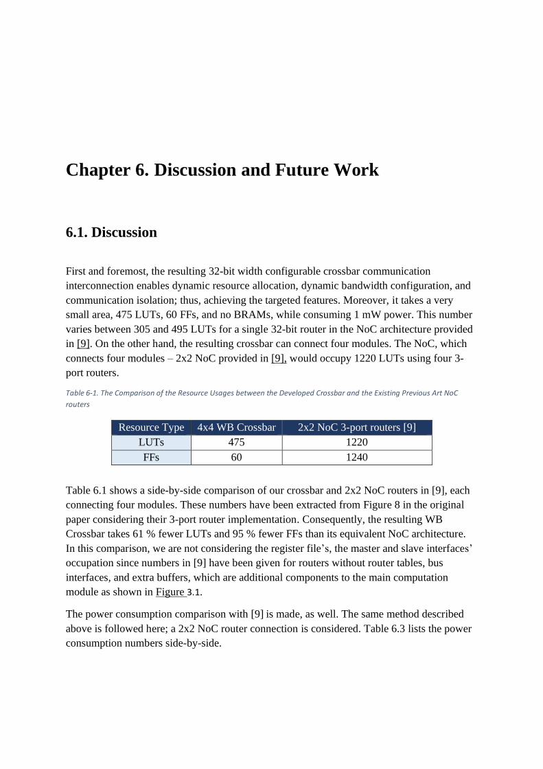
Chapter 6. Discussion and Future Work
6.1. Discussion
First and foremost, the resulting 32-bit width configurable crossbar communication
interconnection enables dynamic resource allocation, dynamic bandwidth configuration, and
communication isolation; thus, achieving the targeted features. Moreover, it takes a very
small area, 475 LUTs, 60 FFs, and no BRAMs, while consuming 1 mW power. This number
varies between 305 and 495 LUTs for a single 32-bit router in the NoC architecture provided
in [9]. On the other hand, the resulting crossbar can connect four modules. The NoC, which
connects four modules – 2x2 NoC provided in [9], would occupy 1220 LUTs using four 3-
port routers.
Table 6-1. The Comparison of the Resource Usages between the Developed Crossbar and the Existing Previous Art NoC
routers
Resource Type 4x4 WB Crossbar 2x2 NoC 3-port routers [9]
LUTs 475 1220
FFs 60 1240
Table 6.1 shows a side-by-side comparison of our crossbar and 2x2 NoC routers in [9], each
connecting four modules. These numbers have been extracted from Figure 8 in the original
paper considering their 3-port router implementation. Consequently, the resulting WB
Crossbar takes 61 % fewer LUTs and 95 % fewer FFs than its equivalent NoC architecture.
In this comparison, we are not considering the register file’s, the master and slave interfaces’
occupation since numbers in [9] have been given for routers without router tables, bus
interfaces, and extra buffers, which are additional components to the main computation
module as shown in Figure 3.1.
The power consumption comparison with [9] is made, as well. The same method described
above is followed here; a 2x2 NoC router connection is considered. Table 6.3 lists the power
consumption numbers side-by-side.
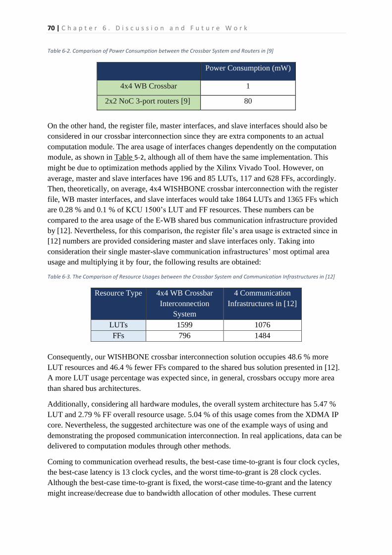
70 | C h a p t e r 6 . D i s c u s s i o n a n d F u t u r e W o r k
Table 6-2. Comparison of Power Consumption between the Crossbar System and Routers in [9]
Power Consumption (mW)
4x4 WB Crossbar 1
2x2 NoC 3-port routers [9] 80
On the other hand, the register file, master interfaces, and slave interfaces should also be
considered in our crossbar interconnection since they are extra components to an actual
computation module. The area usage of interfaces changes dependently on the computation
module, as shown in Table 5-2, although all of them have the same implementation. This
might be due to optimization methods applied by the Xilinx Vivado Tool. However, on
average, master and slave interfaces have 196 and 85 LUTs, 117 and 628 FFs, accordingly.
Then, theoretically, on average, 4x4 WISHBONE crossbar interconnection with the register
file, WB master interfaces, and slave interfaces would take 1864 LUTs and 1365 FFs which
are 0.28 % and 0.1 % of KCU 1500’s LUT and FF resources. These numbers can be
compared to the area usage of the E-WB shared bus communication infrastructure provided
by [12]. Nevertheless, for this comparison, the register file’s area usage is extracted since in
[12] numbers are provided considering master and slave interfaces only. Taking into
consideration their single master-slave communication infrastructures’ most optimal area
usage and multiplying it by four, the following results are obtained:
Table 6-3. The Comparison of Resource Usages between the Crossbar System and Communication Infrastructures in [12]
Resource Type 4x4 WB Crossbar
Interconnection
System
4 Communication
Infrastructures in [12]
LUTs 1599 1076
FFs 796 1484
Consequently, our WISHBONE crossbar interconnection solution occupies 48.6 % more
LUT resources and 46.4 % fewer FFs compared to the shared bus solution presented in [12].
A more LUT usage percentage was expected since, in general, crossbars occupy more area
than shared bus architectures.
Additionally, considering all hardware modules, the overall system architecture has 5.47 %
LUT and 2.79 % FF overall resource usage. 5.04 % of this usage comes from the XDMA IP
core. Nevertheless, the suggested architecture was one of the example ways of using and
demonstrating the proposed communication interconnection. In real applications, data can be
delivered to computation modules through other methods.
Coming to communication overhead results, the best-case time-to-grant is four clock cycles,
the best-case latency is 13 clock cycles, and the worst time-to-grant is 28 clock cycles.
Although the best-case time-to-grant is fixed, the worst-case time-to-grant and the latency
might increase/decrease due to bandwidth allocation of other modules. These current
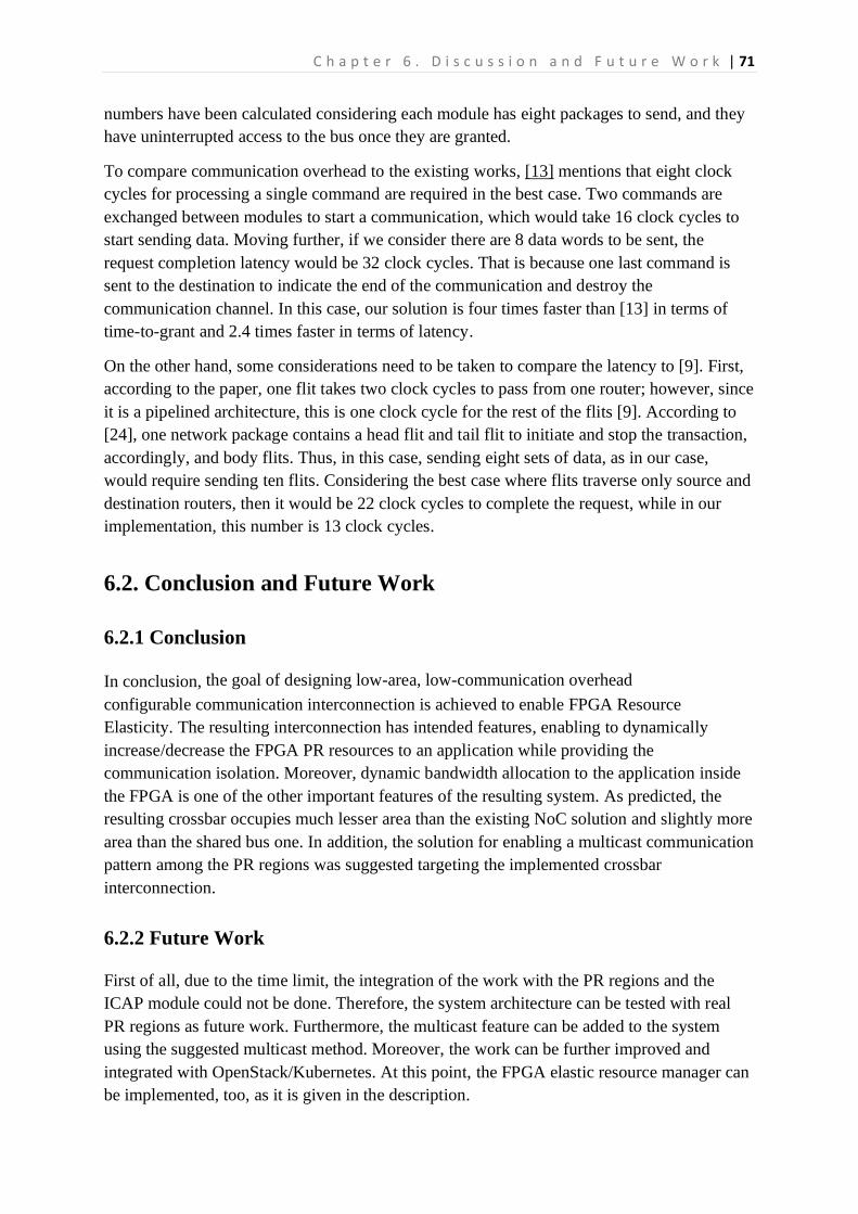
C h a p t e r 6 . D i s c u s s i o n a n d F u t u r e W o r k | 71
numbers have been calculated considering each module has eight packages to send, and they
have uninterrupted access to the bus once they are granted.
To compare communication overhead to the existing works, [13] mentions that eight clock
cycles for processing a single command are required in the best case. Two commands are
exchanged between modules to start a communication, which would take 16 clock cycles to
start sending data. Moving further, if we consider there are 8 data words to be sent, the
request completion latency would be 32 clock cycles. That is because one last command is
sent to the destination to indicate the end of the communication and destroy the
communication channel. In this case, our solution is four times faster than [13] in terms of
time-to-grant and 2.4 times faster in terms of latency.
On the other hand, some considerations need to be taken to compare the latency to [9]. First,
according to the paper, one flit takes two clock cycles to pass from one router; however, since
it is a pipelined architecture, this is one clock cycle for the rest of the flits [9]. According to
[24], one network package contains a head flit and tail flit to initiate and stop the transaction,
accordingly, and body flits. Thus, in this case, sending eight sets of data, as in our case,
would require sending ten flits. Considering the best case where flits traverse only source and
destination routers, then it would be 22 clock cycles to complete the request, while in our
implementation, this number is 13 clock cycles.
6.2. Conclusion and Future Work
6.2.1 Conclusion
In conclusion, the goal of designing low-area, low-communication overhead
configurable communication interconnection is achieved to enable FPGA Resource
Elasticity. The resulting interconnection has intended features, enabling to dynamically
increase/decrease the FPGA PR resources to an application while providing the
communication isolation. Moreover, dynamic bandwidth allocation to the application inside
the FPGA is one of the other important features of the resulting system. As predicted, the
resulting crossbar occupies much lesser area than the existing NoC solution and slightly more
area than the shared bus one. In addition, the solution for enabling a multicast communication
pattern among the PR regions was suggested targeting the implemented crossbar
interconnection.
6.2.2 Future Work
First of all, due to the time limit, the integration of the work with the PR regions and the
ICAP module could not be done. Therefore, the system architecture can be tested with real
PR regions as future work. Furthermore, the multicast feature can be added to the system
using the suggested multicast method. Moreover, the work can be further improved and
integrated with OpenStack/Kubernetes. At this point, the FPGA elastic resource manager can
be implemented, too, as it is given in the description.
72 | R e f e r e n c e s
References
[1] W. J. Dallas and B. Towels, "Chapter 11. Routing Mechanics", in Principles and Practices of Interconnection
Networks, Ed. Elsevier, 2004, p. 203.
[2] "PCI Express", Xilinx, 2021. [Online]. Available: https://www.xilinx.com/products/technology/pci-
express.html#versalpcie. [Accessed: 22- Jul- 2021].
[3] Product Guide: DMA/Bridge Subsystem for PCI Express, v4.1, Xilinx, April 29, 2019. Accessed on: Jul. 22,
2021. [Online]. Available:
https://www.xilinx.com/support/documentation/ip_documentation/xdma/v4_1/pg195-pcie-dma.pdf
[4] Xilinx Answer 71435: DMA Subsystem for PCI Express - Driver and IP Debug Guide, Xilinx, 2018.
Accessed on: Jul. 22, 2021. [Online]. Available:
https://www.xilinx.com/Attachment/Xilinx_Answer_71435_XDMA_Debug_Guide.pdf
[5] P. Fallah, “FPGA Virtualization,” M.S. Thesis, School of Electrical Engineering and Computer Science,
KTH Royal Institute of Technology, Stockholm, 2019. [Online]. Available: http://kth.diva-
portal.org/smash/get/diva2:1412396/FULLTEXT01.pdf
[6] "Xilinx DMA IP Reference drivers", GitHub, 2021. [Online]. Available: GitHub - Xilinx/dma_ip_drivers:
Xilinx QDMA IP Drivers. [Accessed: 22- Jul- 2021].
[7] W. D. Peterson, WISHBONE System-on-Chip (SoC) Interconnection Architecture for Portable IP Cores, B4
ed. OpenCores, 2010. [Online]. Available: Wishbone B4 (opencores.org)
[8] A. S. Lee and N. W. Bergman, "On-chip interconnect schemes for reconfigurable system-on-chip",
in Proceedings of SPIE - The International Society for Optical Engineering, March, 2004. [Online]. Available:
(1) On-chip interconnect schemes for reconfigurable system-on-chip (researchgate.net)
[9] J. M. Mbongue, A. Shuping, P. Bhowmik and C. Bobda, "Architecture Support for FPGA Multi-tenancy in
the Cloud," 2020 IEEE 31st International Conference on Application-specific Systems, Architectures and
Processors (ASAP), 2020, pp. 125-132, doi: 10.1109/ASAP49362.2020.00030. [Online]. Available:
Architecture Support for FPGA Multi-tenancy in the Cloud | IEEE Conference Publication | IEEE Xplore
[10] A. Vaishnav, K. D. Pham, D. Koch and J. Garside, "Resource Elastic Virtualization for FPGAs Using
OpenCL," 2018 28th International Conference on Field Programmable Logic and Applications (FPL), 2018, pp.
111-1117, doi: 10.1109/FPL.2018.00028. [Online]. Available: Resource Elastic Virtualization for FPGAs Using
OpenCL | IEEE Conference Publication | IEEE Xplore
[11] K. Dang Pham, E. Horta and D. Koch, "BITMAN: A tool and API for FPGA bitstream manipulations,"
Design, Automation & Test in Europe Conference & Exhibition (DATE), 2017, 2017, pp. 894-897, doi:
10.23919/DATE.2017.7927114. [Online]. Available: BITMAN: A tool and API for FPGA bitstream
manipulations | IEEE Conference Publication | IEEE Xplore
[12] J. Hagemeyer, B. Kettelhoit, M. Koester and M. Porrmann, "A Design Methodology for Communication
Infrastructures on Partially Reconfigurable FPGAs," 2007 International Conference on Field Programmable
Logic and Applications, 2007, pp. 331-338, doi: 10.1109/FPL.2007.4380668. [Online]. Available: A Design
Methodology for Communication Infrastructures on Partially Reconfigurable FPGAs | IEEE Conference
Publication | IEEE Xplore
[13] A. Ahmadinia et al., "A practical approach for circuit routing on dynamic reconfigurable devices," 16th
IEEE International Workshop on Rapid System Prototyping (RSP'05), 2005, pp. 84-90, doi:
10.1109/RSP.2005.7. [Online]. Available: A practical approach for circuit routing on dynamic reconfigurable
devices | IEEE Conference Publication | IEEE Xplore
R e f e r e n c e s | 73
[14] H. A. ElGindy, A. K. Somani, H. Schroeder, H. Schmeck, and A. Spray. RMB - A Reconfigurable Multiple
Bus Network. In Proceedings of the Second International Symposium on High-Performance Computer
Architecture (HPCA-2), pages 108–117, Feb. 1996. [Online]. Available: RMB-a reconfigurable multiple bus
network | IEEE Conference Publication | IEEE Xplore
[15] G. Agarwal and Ramesh Kini M., "Enhancement of Wishbone protocol with broadcasting and
multicasting," 2015 IEEE International Conference on Electronics, Computing and Communication
Technologies (CONECCT), 2015, pp. 1-5, doi: 10.1109/CONECCT.2015.7383856. [Online]. Available:
Enhancement of Wishbone protocol with broadcasting and multicasting | IEEE Conference Publication | IEEE
Xplore
[16] C. Bobda and A. Ahmadinia, "Dynamic interconnection of reconfigurable modules on reconfigurable
devices," in IEEE Design & Test of Computers, vol. 22, no. 5, pp. 443-451, Sept.-Oct. 2005, doi:
10.1109/MDT.2005.109. [Online]. Available: Dynamic interconnection of reconfigurable modules on
reconfigurable devices | IEEE Journals & Magazine | IEEE Xplore
[17] T. Pionteck, R. Koch and C. Albrecht, "Applying Partial Reconfiguration to Networks-On-Chips," 2006
International Conference on Field Programmable Logic and Applications, 2006, pp. 1-6, doi:
10.1109/FPL.2006.311208. [Online]. Available: Applying Partial Reconfiguration to Networks-On-Chips |
IEEE Conference Publication | IEEE Xplore
[18] T. S. T. Mak, P. Sedcole, P. Y. K. Cheung and W. Luk, "On-FPGA Communication Architectures and
Design Factors," 2006 International Conference on Field Programmable Logic and Applications, 2006, pp. 1-8,
doi: 10.1109/FPL.2006.311209. [Online]. Available: On-FPGA Communication Architectures and Design
Factors | IEEE Conference Publication | IEEE Xplore
[19] User Guide: KCU1500 Board, v1.4, Xilinx, April 12, 2018. Accessed on: Jul. 22, 2021. [Online].
Available: KCU1500 Board User Guide (UG1260) (xilinx.com)
[20] V. Lahtinen, E. Salminen, K. Kuusilinna and T. Hamalainen, "Comparison of synthesized bus and crossbar
interconnection architectures," Proceedings of the 2003 International Symposium on Circuits and Systems,
2003. ISCAS '03., 2003, pp. V-V, doi: 10.1109/ISCAS.2003.1206307. [Online]. Available: Comparison of
synthesized bus and crossbar interconnection architectures | IEEE Conference Publication | IEEE Xplore
[21] G. Dimitrakopoulos, C. Kachris and E. Kalligeros, "Scalable Arbiters and Multiplexers for On-FGPA
Interconnection Networks," 2011 21st International Conference on Field Programmable Logic and Applications,
2011, pp. 90-96, doi: 10.1109/FPL.2011.26. [Online]. Available: Scalable Arbiters and Multiplexers for On-
FGPA Interconnection Networks | IEEE Conference Publication | IEEE Xplore
[22] Kyeong Keol Ryu, Eung Shin and V. J. Mooney, "A comparison of five different multiprocessor SoC bus
architectures," Proceedings Euromicro Symposium on Digital Systems Design, 2001, pp. 202-209, doi:
10.1109/DSD.2001.952283. [Online]. Available: A comparison of five different multiprocessor SoC bus
architectures | IEEE Conference Publication | IEEE Xplore
[23] V. G. Oklobdzija, "An algorithmic and novel design of a leading zero detector circuit: comparison with
logic synthesis," in IEEE Transactions on Very Large Scale Integration (VLSI) Systems, vol. 2, no. 1, pp. 124-
128, March 1994, doi: 10.1109/92.273153. [Online]. Available: An algorithmic and novel design of a leading
zero detector circuit: comparison with logic synthesis | IEEE Journals & Magazine | IEEE Xplore
[24] W. J. Dallas and B. Towels, "Chapter 12. Flow Control Basics", in Principles and Practices of
Interconnection Networks, Ed. Elsevier, 2004, p. 224.

74 | A P P E N D I X
APPENDIX A
Register File Description
This register file was prepared considering three PR regions connected to ports 1,2,3 and the
PCIe slot connected to port 0 as given in the implementation description. Access types are
given from the host side's perspective. Only the FPGA logic can update the registers which
have read access-type.
Table A-1. Register File Description
N Register
Address
Information Stored Default Value Access
Type
Notes
0 0x0 FPGA device ID 0xFACE0103 R
1 0x4 PR region 1 destination address 0x1 R/W
By default, all PR regions
send data to the PCIe slot 2 0x8 PR region 2 destination address 0x1 R/W
3 0xC PR region 3 destination address 0x1 R/W
4 0x10 Reset PR regions and ports [3:0] 0xFFFFFFFF R/W Resets are active low
5 0x14 Allowed Addresses of Port 0 Master 0xF R/W PCIe slot can access all ports
6 0x18 Allowed Addresses of Port 1 Master 0x1 R/W By default, all PR regions can
send data to the PCIe slot
only 7 0x1C Allowed Addresses of Port 2 Master 0x1 R/W
8 0x20 Allowed Addresses of Port 3 Master 0x1 R/W
9 0x24 Package numbers allowed in port 0 for
ports [3:0]
0x08080808 R/W Eight bits are reserved for
each port-to-port
communication. For ex., port
1 can send eight packs (08) to
port 0, but 0 packs to port 1-
to-3 (00)
10 0x28 Package numbers allowed in port 1 for
ports [3:0]
0x00000008 R/W
11 0x2C Package numbers allowed in port 2 for
ports [3:0]
0x00000008 R/W
12 0x30 Package numbers allowed in port 3 for
ports [3:0]
0x00000008 R/W
13 0x34 Application ID 0 destination address 0x1 R/W By default, all data sent to
XDMA is looped back to the
server. 14 0x38 Application ID 1 destination address 0x1 R/W
15 0x3C Application ID 2 destination address 0x1 R/W
16 0x40 Application ID 3 destination address 0x1 R/W
17 0x44 PR region [3:1] last transaction error
status
0x0 R Eight bits are reserved for
each PR region, i.e., bits [7:0]
for PR 1, [15:8] for PR 2
18 0x48 App. ID [3:0] last transaction error
status
0x0 R Eight bits are reserved for
each app ID.
19 0x4C ICAP status 0x0 R It indicates if the ICAP
module completed
reconfiguration or gave an
error.
If bit 0 is high, it is done; if
bit 1 is high, it gives an error.
The rest is not used

Related Documents


![Topic 4 Elasticity - Trinity College, Dublin · PDF filePrice Elasticity of Demand ... Price Elasticity of Supply ... Microsoft PowerPoint - Topic 4 Elasticity [Compatibility Mode]](https://static.cupdf.com/doc/110x72/5ab680a27f8b9a6e1c8dc1e4/topic-4-elasticity-trinity-college-dublin-elasticity-of-demand-price-elasticity.jpg)