New Jersey Institute of Technology New Jersey Institute of Technology Digital Commons @ NJIT Digital Commons @ NJIT Theses Electronic Theses and Dissertations 10-31-1993 Hardware design for JPEG and a comparative study of JPEG and Hardware design for JPEG and a comparative study of JPEG and MPEG image compression algorithms MPEG image compression algorithms Aravind Soundararajan New Jersey Institute of Technology Follow this and additional works at: https://digitalcommons.njit.edu/theses Part of the Electrical and Electronics Commons Recommended Citation Recommended Citation Soundararajan, Aravind, "Hardware design for JPEG and a comparative study of JPEG and MPEG image compression algorithms" (1993). Theses. 1946. https://digitalcommons.njit.edu/theses/1946 This Thesis is brought to you for free and open access by the Electronic Theses and Dissertations at Digital Commons @ NJIT. It has been accepted for inclusion in Theses by an authorized administrator of Digital Commons @ NJIT. For more information, please contact [email protected].

Welcome message from author
This document is posted to help you gain knowledge. Please leave a comment to let me know what you think about it! Share it to your friends and learn new things together.
Transcript
New Jersey Institute of Technology New Jersey Institute of Technology
Digital Commons @ NJIT Digital Commons @ NJIT
Theses Electronic Theses and Dissertations
10-31-1993
Hardware design for JPEG and a comparative study of JPEG and Hardware design for JPEG and a comparative study of JPEG and
MPEG image compression algorithms MPEG image compression algorithms
Aravind Soundararajan New Jersey Institute of Technology
Follow this and additional works at: https://digitalcommons.njit.edu/theses
Part of the Electrical and Electronics Commons
Recommended Citation Recommended Citation Soundararajan, Aravind, "Hardware design for JPEG and a comparative study of JPEG and MPEG image compression algorithms" (1993). Theses. 1946. https://digitalcommons.njit.edu/theses/1946
This Thesis is brought to you for free and open access by the Electronic Theses and Dissertations at Digital Commons @ NJIT. It has been accepted for inclusion in Theses by an authorized administrator of Digital Commons @ NJIT. For more information, please contact [email protected].

Copyright Warning & Restrictions
The copyright law of the United States (Title 17, United States Code) governs the making of photocopies or other
reproductions of copyrighted material.
Under certain conditions specified in the law, libraries and archives are authorized to furnish a photocopy or other
reproduction. One of these specified conditions is that the photocopy or reproduction is not to be “used for any
purpose other than private study, scholarship, or research.” If a, user makes a request for, or later uses, a photocopy or reproduction for purposes in excess of “fair use” that user
may be liable for copyright infringement,
This institution reserves the right to refuse to accept a copying order if, in its judgment, fulfillment of the order
would involve violation of copyright law.
Please Note: The author retains the copyright while the New Jersey Institute of Technology reserves the right to
distribute this thesis or dissertation
Printing note: If you do not wish to print this page, then select “Pages from: first page # to: last page #” on the print dialog screen

The Van Houten library has removed some of the personal information and all signatures from the approval page and biographical sketches of theses and dissertations in order to protect the identity of NJIT graduates and faculty.
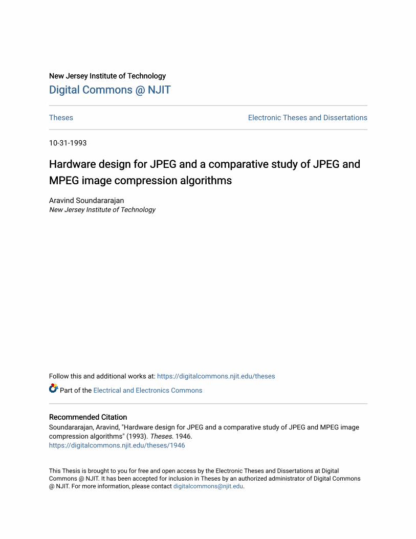
ABSTRACT
JPEG Hardware Design and a Comparative Study of JPEG and MPEG Image Compression Algorithms
by
Aravind Soundararajan
The complete PC-based hardware design along with the initialization and control
software of the JPEG algorithm is presented in this thesis. The hardware could run in
real-time to compress, decompress and display still frame images. LSI Logic JPEG
chipset was used in the design. This is a dedicated chipset for the JPEG compression
algorithm.
A simulation software was used for studying the performance of MPEG video
compression algorithm. Various video test sequences were compressed through the codec
simulation software and the resulting rate-distortion performance was calculated. These
are compared with the performance of JPEG based image sequence compressor.
It is found that the MPEG-based video codec significantly outperforms the JPEG-
based codec for the test sequences considered at low to medium bit rates.
HARDWARE DESIGN FOR JPEG
AND A COMPARATIVE STUDY OF JPEG AND MPEG
IMAGE COMPRESSION ALGORITHMS
by
Aravind Soundararajan
A Thesis Submitted to the Faculty of
New Jersey Institute of Technology in Partial Fulfillment of the Requirement for the Degree of
Master of Science in Electrical Engineering
Department of Electrical and Computer Engineering
October 1993

APPROVAL PAGE
Hardware Design for JPEG and a Comparative Study of JPEG and MPEG Algorithms
Aravind Soundararajan
Dr.Ali N. Akansu, Thesis Advisor (date) Associate Professor of Electrical Engineering, NJIT
Dr.Yeheskel Bar-Ness, Committee Member (date) Distinguished Professor of Electrical Engineering, NJIT
Dr.David Cooper, Committee Member (date) GEC Marconi Electronic Systems Corporation, Totowa, NJ
BIOGRAPHICAL SKETCH
Author: Aravind Soundararajan
Degree: Master of Science in Electrical Engineering.
Date: October 1993
Undergraduate and Graduate Education:
• Master of Science in Electrical Engineering, New Jersey Institute of Technology, Newark, NJ, 1993
• Bachelor of Science in Electronics and Communication Engineering. Regional Engineering College, Trichy, India, 1990
Major: Electrical Engineering.
Presentations and Publications:
Soundararajan Aravind, " Image Processing in Intra Venous Cerebral Angiography." IEEE Symposium , PSNA College of Engineering, Dindigul, India , January 1990
iv

This thesis is dedicated to my parents and my brother
v

ACKNOWLEDGEMENT
I would like to thank my advisor Dr. Ali N. Akansu, for his invaluable
advice, guidance and support in making this thesis a very rewarding and
successful one. I also appreciate his constant questioning and recommendations
which made this work and my educational goals more meaningful. I have learned
a great deal from him not only academically but also in other general aspects of
life.
I am highly grateful to Andria Wong and Fure Ching Jeng from Bellcore,
Morristown for their cooperation in providing the MPEG simulation software and
during the various stages of the project.
I also thank the committee members - Dr. Bar-Ness and Dr. Cooper who
spared some of their valuable time to go through my report and give suggestions.
I am grateful to Ronald Buell , David Cooper and Mark D'amato for the
help and facilities they rendered while at GEC in addition to their cooperation
without which this project could never have become a reality.
Thanks and regards to my parents for their moral support and love and
also to my labmates Adil, Mehmet, Ferhat and Nadir who made the period of this
work a pleasant one.
vi
TABLE OF CONTENTS Chapter Page
1 INTRODUCTION 1
2 JPEG STANDARD 4
2.1 Color Systems 4
2.2 The Baseline System 4
2.3 DCT 7
2.3.1 Models for DCT based systems .................................................................... 8
2.3.2 Level shift 10
2.4 Variable Length Coding ( Huffman Coding ) 10
3 JPEG HARDWARE 12
3.1 Terms and Concepts 12
3.2 Typical System Application 20
3.3 Color and Raster-Block Converter 22
3.3.1 RGB Interface 22
3.3.2 Conversion Logic 24
3.3.3 Strip Memory Interface 24
3.3.4 YCbCr Interface 25
3.3.5 Internal Registers 25
3.3.6 Control Signals 25
3.4 Configuration and Control 26
3.4.1 Address Register 26
3.4.2 Gamma Correction Table 27
3.4.3 Configuration Registers. 30
3.4.4 Window Control Registers 32
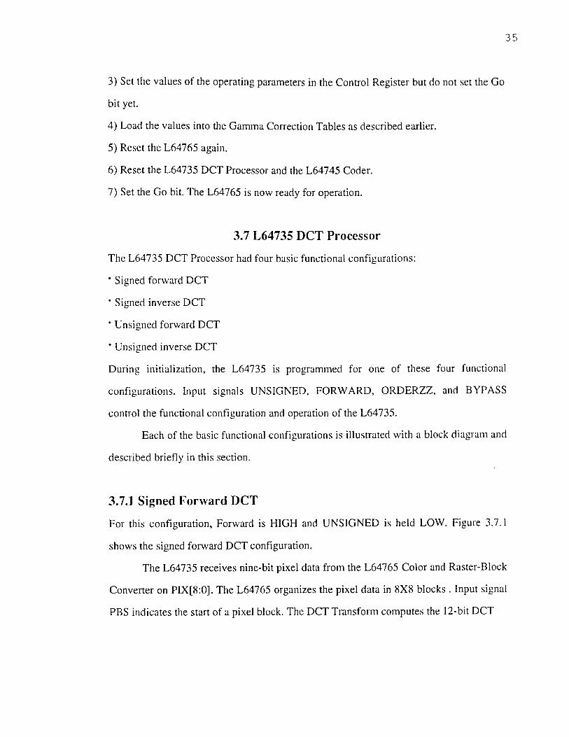
3.5 Reset Operation 34
3.6 Initialization Sequence 34
vii
Chapter Page
3.7 L64735 DCT Processor 35
3.7.1 Signed Forward DCT 35
3.7.2 Signed Inverse DCT 37
3.7.3 Unsigned Inverse and Forward DCT 37
3.7.4 Signal Descriptions 37
3.8 Configuration and Control 40
3.9 L64735 Operation modes 40
3.10 JPEG Coder (L64745) 42
3.10.1 Signal Description 42
3.10.2 Code Interface Signals 45
3.10.3 Control Signals. 46
3.11 Configuration and Control . 47
3.11.1 Group ID Word 47
3.12 Hardware Description 55
3.12.1 Operation 55
4 MPEG STANDARD 56
4.1 MPEG Overview 56
4.2 Basic Concepts . 58
4.3 Simplified Decoder Model 62
4.4 Preprocessing 63
4.5 Conversion from CCIR601 video 65
4.6 Motion Compensation and Estimation . 67
4.7 Motion Estimation 70
4.8 Coding of Motion Vectors . 72
5 RESULTS AND CONCLUSIONS 75
5.1 Hardware Implementation 75
viii
Chapter Page
5.2 Simulations 75
5.3 Conclusions and Future Directions 75
6 APPENDIX 81
7 REFERENCES 112
ix
LIST OF FIGURES Figure Page
2.1 JPEG Block Diagram. 5
2.2.1 Baseline DCT Based JPEG System .................................................................. 6
2.3.1 Models for DCT Based Systems. 9
3.1 JPEG Chipset in Encoder Application. 14
3.1.1 Active Image Area 14
3.1.2 Typical Image Correction Function 15
3.1.3 Block Procesing by L64765 18
3.1.4 Data Interleaving. 19
3.1.5 Block Input Ordering 19
3.2.1 Typical System Application. 21
3.3.1 L64765 Logic Symbol 23
3.4.1 Address Register Write 28
3.4.2 Gamma Table Read and Write. 29
3.4.3 Control Register 31
3.5.1 Reset Operation ............................................................................................. 36
3.7.1 Signed Forward DCT Configuration. 36
3.7.2 Signed Inverse DCT Configuration 38
3.7.3 Unsigned Forward DCT Configuration 38
3.7.4 Unsigned Inverse DCT Configuration 38
3.9.1 Forward DCT Configuration. 44
3.9.2 Forward DCT Output Waveforms. 44
3.9.3 Inverse DCT Waveforms ................................................................................ 44
3.11.1 Read Initialization Sequence 48
3.11.2 Write Initialization Sequence. 48
3.11.3 Configuration Group Format 49
Figure Page
3.12.1a Hardware Description 52
3.12.1b Hardware Description. 53
3.12.1c Hardware Description 54
4.1 Overview of MPEG Coding. 57
4.2.1 Macro Block Structure. 59
4.2.2 Block Structure. 59
4.2.3 Typical Sequence of Pictures in Bitstream Order. 61
4.3.1 Simplified Decoder Implementation ............................................................ 61
4.4.1 Typical Sequences of Pictures in Display Order 64
4.4.2 Typical Sequence of Pictures in Bitstream Order. 64
4.4.3 Coding and Decoding Process ..................................................................... 66
4.5.1 Source Input Format with Significant Pel Area Shaded Dark 66
4.6.1 Group of Pictures in Display Order 68
5.1 JPEG Simulations ........................................................................................ 76
5.2 MPEG Simulations 77
xi
LIST OF TABLES Table Page
3.4.1 Configuration Addresses 31
3.4.2 Data Formats 33
3.8.1 Configuration Inputs 41
3.10.1 FIFOST[1:0] Status in Encoder Configuration. 43
4.8.1 Code for Forward_f or Backward_f equal to 1,2,3 ........................................ 71
4.8.3 Modulus for Motion Vectors . 74
5.1 JPEG Simulations 78
5.2 MPEG Simulations . 79
xi
Chapter 1
INTRODUCTION
Mankind is continuously trying to transfer information at a rapid rate . The need to transfer
data rapidly often necessitates that information be sent over a channel at a rate that exceeds
the channel capacity. Some distortion inevitably results in such situations. In order to keep
this distortion to a minimum level, we must first order the data generated by the source in
accordance with it's importance at the receiver, and then either compress or discard the less
significant information prior to transmission. The schemes devised to extract the significant
information from the output of source and to reduce redundancy are called source coding
algorithms.
With the recent advances in modern communications, signal processing and VLSI
technologies the transmission and storage of real time video has become a reality. Typical
Color Television or video-conferencing images have a spatial resolution of approximately
512 X 512 pixels per frame with 24 bits/pixel resolution and requires 30 frames/second to
avoid any jerky motion of the picture. This is equivalent to the data rate of about 180 X 106
bits per second. Thus the channel capacity of 106 bits/second to 108 bits/second may be
needed depending on the application.The transmission and storage of such a large amount of
data requires data compression algorithms.
The primary application of data compression is in the transmission and storage of
information.Image transmission applications span the broadcast television, remote sensing
via satellites, teleconferencing, computer communications, facsimile transmission and others.
The compression techniques of these applications should consider the size and complexity
of the required hardware.
Video Compression methods exploit on source redundancies and the characteristics of
Human Visual System (HVS). The correlation in still images and in spacio-temporal
correlations in video signals are reduced. The reduction in correlation in spatial domain is
1
2
called intra-frame compression, while compression in temporal domain is called inter-frame
compression. Generally, the methods that achieve high compression ratios (10:1 to 50:1 for
images and 50:1 to 200:1 for video) are lossy such that the reconstructed data are not
identical to the original.
Lossless methods do exist, but their compression ratios are far lower, perhaps no better
than 3:1. Such techniques are used only in sensitive applications such as medical images. For
example , artifacts introduced by a lossy algorithm into an X-ray radiograph may suggest an
incorrect interpretation and alter the diagnosis of a medical condition. Conversely, for
commercial, industrial and consumer applications, lossy algorithms are preferred because
they save on memory and communication bandwidth.
These lossy algorithms also generally exploit aspects of the human visual system. For
example, the eye is much more receptive to fine details in the luminance (or brightness)
signal than in the chrominance (or color) signals. Consequently, the luminance signal is
usually sampled at a higher spatial resolution. In broadcast quality television , the digital
resolution of the sampled luminance signal is 720 X 480 pixels, while for the color signals it
maybe only 360 X 240 pixels. Second, the encoded (or compressed) representation of the
luminance signal is assigned more bits (a higher dynamic range) than the chrominance
signals.
Also, the eye is less sensitive to energy with high spatial frequency than with the low
spatial frequency. Indeed, if an image on a 13 inch personal computer monitor were formed
by an alternating spatial signal of black and white, the human viewer would see a uniform
gray instead of the alternating checkerboard pattern. This deficiency is exploited by coding
the high frequency coefficients with fewer bits and the low ones with more bits.
All these techniques add up to powerful lossy compression algorithms. In many subjective
tests, reconstructed images that were encoded at 20:1 compression ratio are hard to
distinguish from the original. Video data, even after compression at ratios of 10 : 1, can be
decompressed with close to the analog tape quality.
There are various standard Image compression schemes. These are :
1) CCITT H.261 : The H.261 standard of the International Consultative Committee for
Telephones and Telegraphs (CCITT) specifies a method of communication for visual images
and makes use of motion compensation and adaptive Discrete Cosine Transform(ADCT).
2) JPEG : The Joint Photographic Experts Group (JPEG) formed in 1986, has proposed an
international standard for the compression of continuous tone (gray scale or color) images.
The transform used is the Discrete Cosine Transform along with Huffman variable length
codes.
3) MPEG : Moving Pictures Expert Group ( MPEG) proposed an international standard for
motion pictures which made use of motion estimation and compensation techniques leading
to greater reduction in the redundancy than the JPEG. This also makes use of the DCT.
The following chapters are organized as follows. Chapter 2 explains the JPEG algorithm,
Discrete Cosine Transform and Huffman coding techniques. Chapter 3 explains the
Hardware designed for the JPEG algorithm. Chapter 4 deals with the MPEG algorithm.
Chapter 5 explains the simulations performed and the results of the simulations . This also
gives the conclusions and the future directions for research.
The objective of this thesis is to design the hardware for the real time compression and
decompression of image sequences and to compare the performance of JPEG and MPEG
based codecs on the same test sequence. Based on the simulations done it has been
outrightly proved that MPEG based systems perform much better than the JPEG based ones
for the same bits/pel and same test sequence. The tables of the Signal to Noise ratios for the
two cases are shown in Chapter 5.
3
Chapter 2
JPEG STANDARD
JPEG stands for the Joint Photographic Experts Group Committee which is a research
team formed under the auspices of the International Standards Organization (ISO).The
proposed standard is a still picture coding algorithm . The scope of the algorithm is
broad- it comprises a baseline lossy approach and an extended lossless approach, as well
as independent functions using different coding techniques than the baseline scheme. The
hardware developed in this work falls under the lossy baseline approach. The JPEG
algorithm is depicted in Fig 2.1.
2.1 Color Systems
The JPEG algorithm falls under the heading of transform-based image coding. A color
image can be represented in different color formats. Those which are widely used today
include R-G-B (the three primary colors red , green and blue) in the computer industry;
Y-U-V ( Y for luminance, U and V for the color difference signals Y-R and Y-B
respectively ) in the television industry; and the C-M-Y-K (cyan, magenta, yellow and
black) in the printing industry. Within each color system, the constituent parts are called
components. Thus, there are three color components in the R-G-B system and four in the
C-M-Y-K system.
2.2 The Baseline System
A "baseline system" as shown in Fig 2.2.1 is defined as one which guarantees that a
reasonable level of function will be present in all decoders which use the DCT
algorithms. This baseline system uses a constrained version of the sequential DCT
algorithms. The baseline system must be present in all systems which use the DCT
compression algorithms.
4
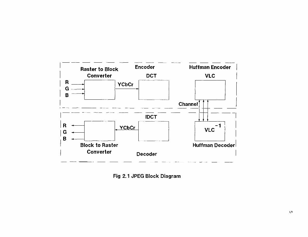
Fig 2.1 JPEG Block Diagram
5
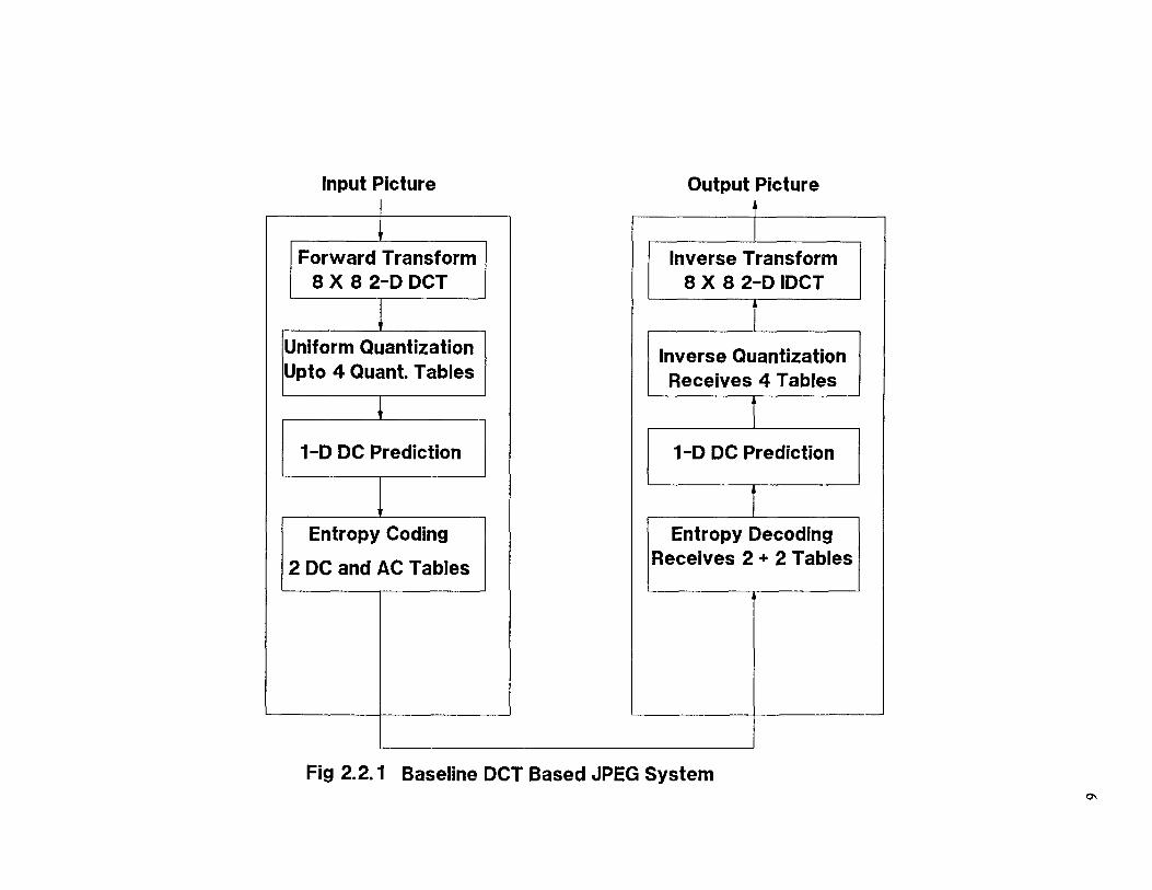
Fig 2.2.1 Baseline DCT Based JPEG System
6
7
The baseline DCT system capabilities can be extended in a number of ways.These so
called "extended systems" can use progressive modes of compression, higher precision,
and an alternative coding techniques. They have a fewer constraints than the baseline
system in several other important parts of the system.
A separate lossless coding algorithm is defined which uses a DPCM (Differential
Pulse Code Modulation) algorithm. In this case the subsequent sample values are
predicted based on the previous sample values. The baseline DCT system is not required
in a lossless decoding system.
The compression achieved with these algorithms depends on the characteristics of the
test images. For the color images of natural scenes which have been used for testing and
development of the algorithms, recognizable images are obtained at about 0.15 bits per
pixel and acceptable quality images are obtained at about 0.25 bits per pixel. At 0.75 bits
per pixel, the image quality is very good, and at about 1.5 bits per pixel the images
obtained are essentially indistinguishable from the original source. Lossless compression
ratio is about 2:1 for these test images. All of these experiments are based on tests of
4:2:2 CCIR601 format Y,Cb,Cr color images with 16 bits per pixel.
Chapter 5 gives the results of the simulations performed with CCIR601 test images on
the JPEG board and the MPEG simulation software.
2.3 DCT
The term image transform usually refers to a class of unitary matrices used for
representing images. One-dimensional signal can be represented by an orthogonal series
of basis functions, an image can also be expanded in terms of a discrete set of basis
arrays called basis images. These basis images can be generated by unitary matrices [2].
To make the transform coding practical, a given image is divided into NM/pq blocks,
each of size p x q, the main storage requirements for implementing the transform are
reduced by a factor of MN/pq. The computational load is reduced by a factor of
8
log2MN/log2pq for fast transform requiring a Nlog2 operations to transform an N X 1
vector. For 256 X 256 images divided into 8 X 8 blocks, these factors are 1024 and 2.66
respectively [4]. Although the operation count is not greatly reduced, the complexity of
the hardware for implementing small size transform is reduced significantly. However,
smaller block sizes yield lower compression.
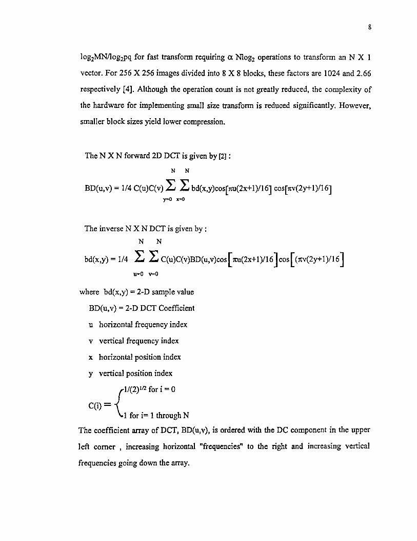
The N X N forward 2D DCT is given by [2] :
The inverse N X N DCT is given by :
where bd(x,y) = 2-D sample value
BD(u,v) = 2-D DCT Coefficient
u horizontal frequency index
v vertical frequency index
x horizontal position index
y vertical position index
The coefficient array of DCT, BD(u,v), is ordered with the DC component in the upper
left corner , increasing horizontal "frequencies" to the right and increasing vertical
frequencies going down the array.
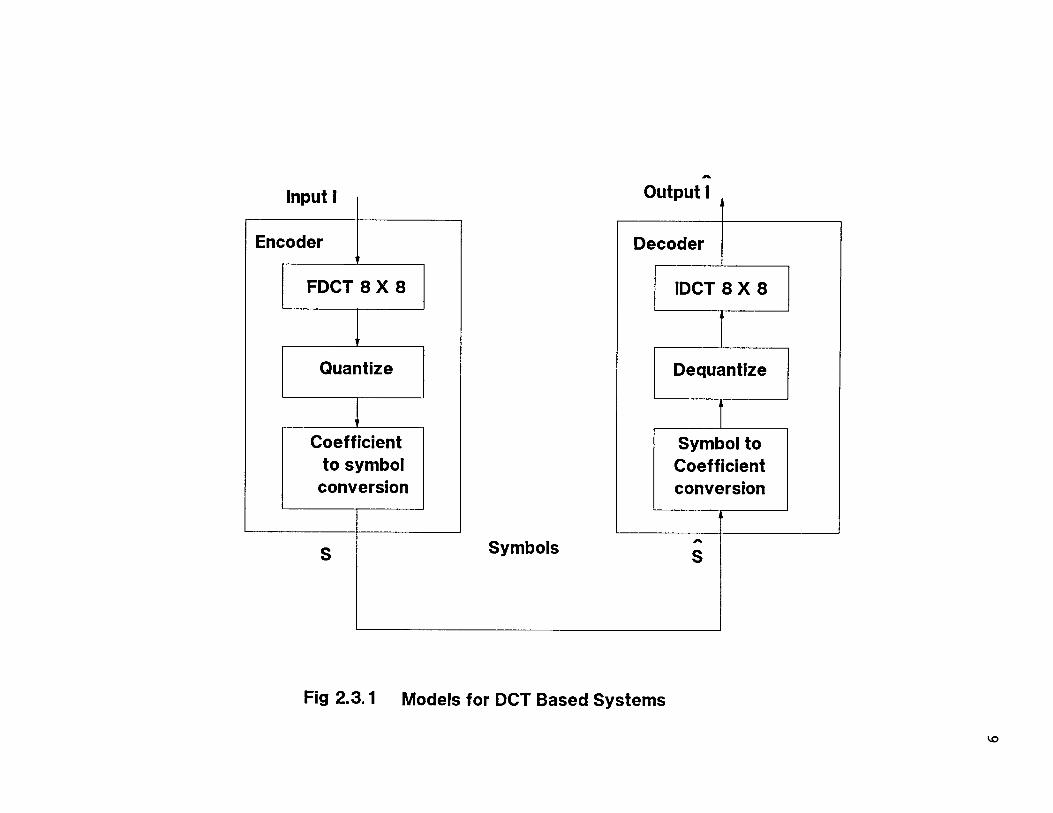
Fig 2.3.1 Models for DCT Based Systems
9
10
2.3.1 Models for DCT Based Systems
The DCT based systems can be divided into three parts, as shown in fig 2.3.1. In the
encoder 8 X 8 blocks of 2D input array samples are transformed using the forward DCT
(FDCT). The DCT coefficients are quantized based on their variances and visual weights.
The quantizer output is mapped to a set of symbols.
In the decoder the symbols are decoded by the entropy decoder and quantized DCT
coefficients values are obtained. The inverse DCT (IDCT) then transforms the 8 X 8
DCT array back into an 8 X 8 array of signal values.
The distortion between I and I' in fig 2.3.1, is governed entirely by the FDCT,
quantization, dequantization and IDCT procedures, with the assumption of an error free
transmission.
2.3.2 Level Shift
The source image input data have an unsigned representation. When coding unsigned
data with P bits of precision, the input data is level shifted by subtracting 2(P-1) before
processing with the forward DCT. For 8 bit precision, 128 is subtracted and for 12 bit
precision 2048 is subtracted. After processing with the IDCT, the same level shift must
be added to the output values to obtain the unsigned representation. Overflow and
underflow of the IDCT output due to the hardware limitations must be appropriately
clamped.
2.4 Variable-Length Coding ( Huffman Coding )
JPEG encoder uses variable length coding or Huffman coding. The code words are
chosen to maximize the compression for the image data type to be processed. The most
commonly occurring events are assigned with the shortest code words. Each symbol
supplied by the model is coded using a particular code word chosen from the table.

11
The tables used by the Huffman coding technique are constructed from information
and they are included in the signalling parameters. It is, therefore, possible to create
Huffman tables which are appropriate for a class images, or even specifically optimized
for each individual image.
In the baseline system up to two tables may be used for DC coefficient coding and up
to two tables can be used for AC coefficient coding. In the extended system, up to four
DC tables and four AC tables may be used.
Tables may be inherited from previous images and from previous stages. Thus, a set
of tables may be used for a sequence of images.
12
Chapter 3
JPEG HARDWARE IMPLEMENTATION
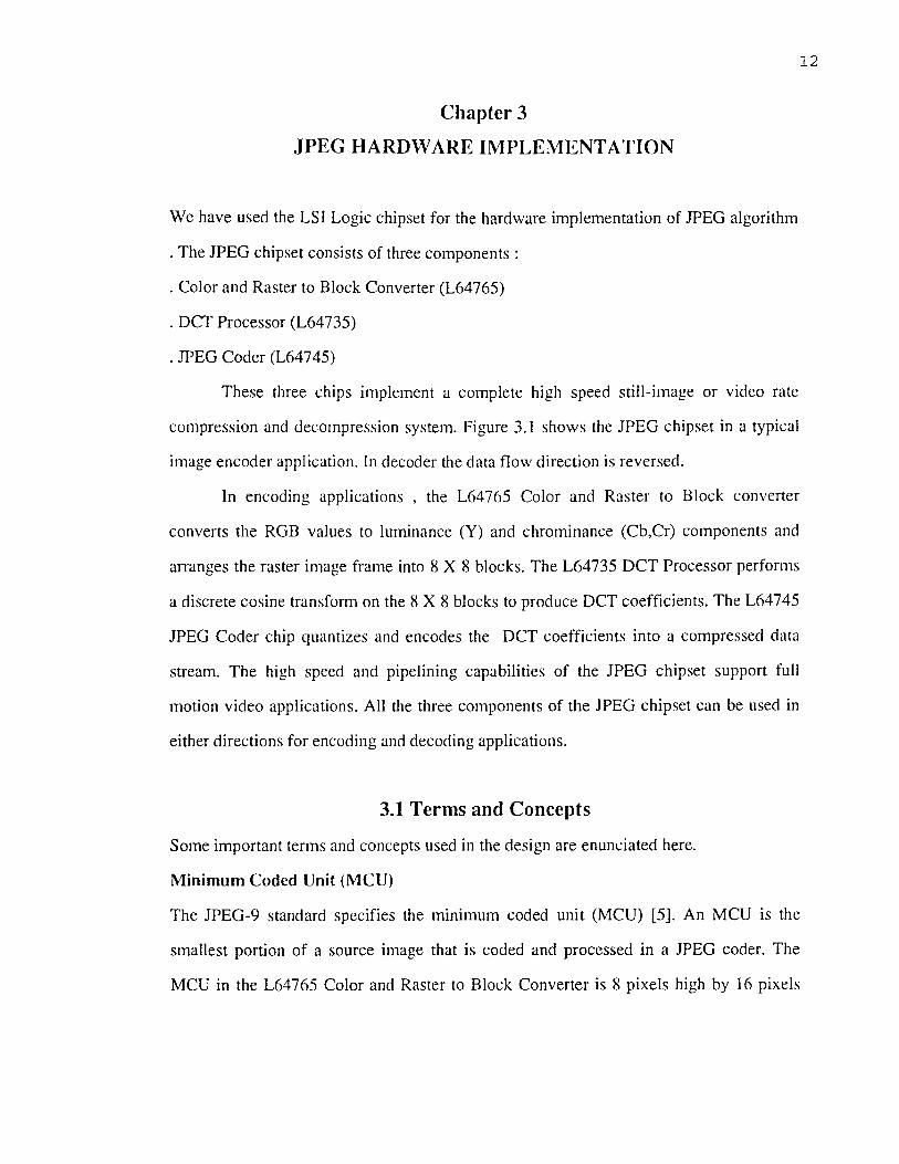
We have used the LSI Logic chipset for the hardware implementation of JPEG algorithm
. The JPEG chipset consists of three components :
. Color and Raster to Block Converter (L64765)
. DCT Processor (L64735)
. JPEG Coder (L64745)
These three chips implement a complete high speed still-image or video rate
compression and decompression system. Figure 3.1 shows the JPEG chipset in a typical
image encoder application. In decoder the data flow direction is reversed.
In encoding applications , the L64765 Color and Raster to Block converter
converts the RGB values to luminance (Y) and chrominance (Cb,Cr) components and
arranges the raster image frame into 8 X 8 blocks. The L64735 DCT Processor performs
a discrete cosine transform on the 8 X 8 blocks to produce DCT coefficients. The L64745
JPEG Coder chip quantizes and encodes the DCT coefficients into a compressed data
stream. The high speed and pipelining capabilities of the JPEG chipset support full
motion video applications. All the three components of the JPEG chipset can be used in
either directions for encoding and decoding applications.
3.1 Terms and Concepts
Some important terms and concepts used in the design are enunciated here.
Minimum Coded Unit (MCU)
The JPEG-9 standard specifies the minimum coded unit (MCU) [5]. An MCU is the
smallest portion of a source image that is coded and processed in a JPEG coder. The
MCU in the L64765 Color and Raster to Block Converter is 8 pixels high by 16 pixels
13
wide in the fixed 2:1:1 format. Each MCU contains two data blocks of the luminance
(intensity) and one data block each of the chrominance (Cb,Cr) color components.
Active Image area
In many applications, only a portion of the source image , the active image area is
processed. The L64765 Color and Raster to Block Converter defines the active image
area in terms of the four parameters : height , width, height delay, and the width delay.
Figure 3.1.1 shows the definition of these parameters relative to the complete image. The
height and width delays are measured in pixels. The height and width are measured in
MCUs. The shaded portion of the frame is said to be blanked. Blanked portions are
ignored by the L64765 and are not sent to the L64735 DCT Processor.
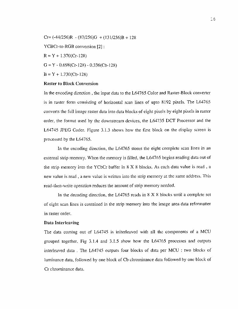
Gamma Correction
To compensate the non-linear response of recording and display equipment, it is usually
necessary to apply a gamma correction to the image data. Gamma correction is a non-
linear gain function . The L64765 applies the Gamma correction using a look up gamma
correction table implemented in the internal RAM. Figure 3.1.2 shows a typical Gamma
correction function.
Color Conversion
The RGB-to-YCbCr and the vice versa color conversions are defined in the CCIR 601
recommendations. The first set of equations shows the RGB-to-YCbCr color conversion
as a set of linear equations. The second set of equations transforms YCbCr-to-RGB color
components. RGB and Y values are within the interval of 16 to 235 (inclusive); Cb and
Cr values are in the range of 16 to 240 (inclusive). Any computation result that exceeds
these values will be clipped to the boundary to eliminate any overflow or underflow
occurrences.
RGB-to-YCbCr conversion [2] :
Y = (77/256)R + (150/256)G + (29/256)B
Cb= (131/256)R + (110/256)G - (21/256)B + 128
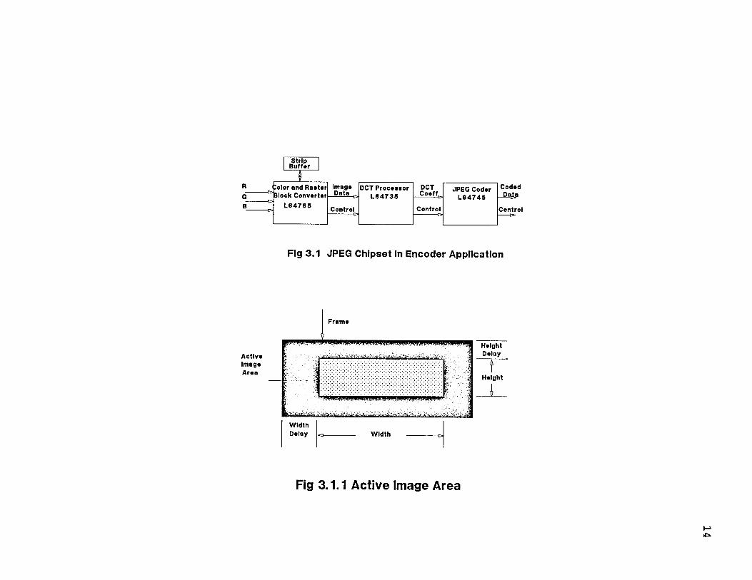
Fig 3.1 JPEG Chipset in Encoder Application
Fig 3.1.1 Active Image Area
14
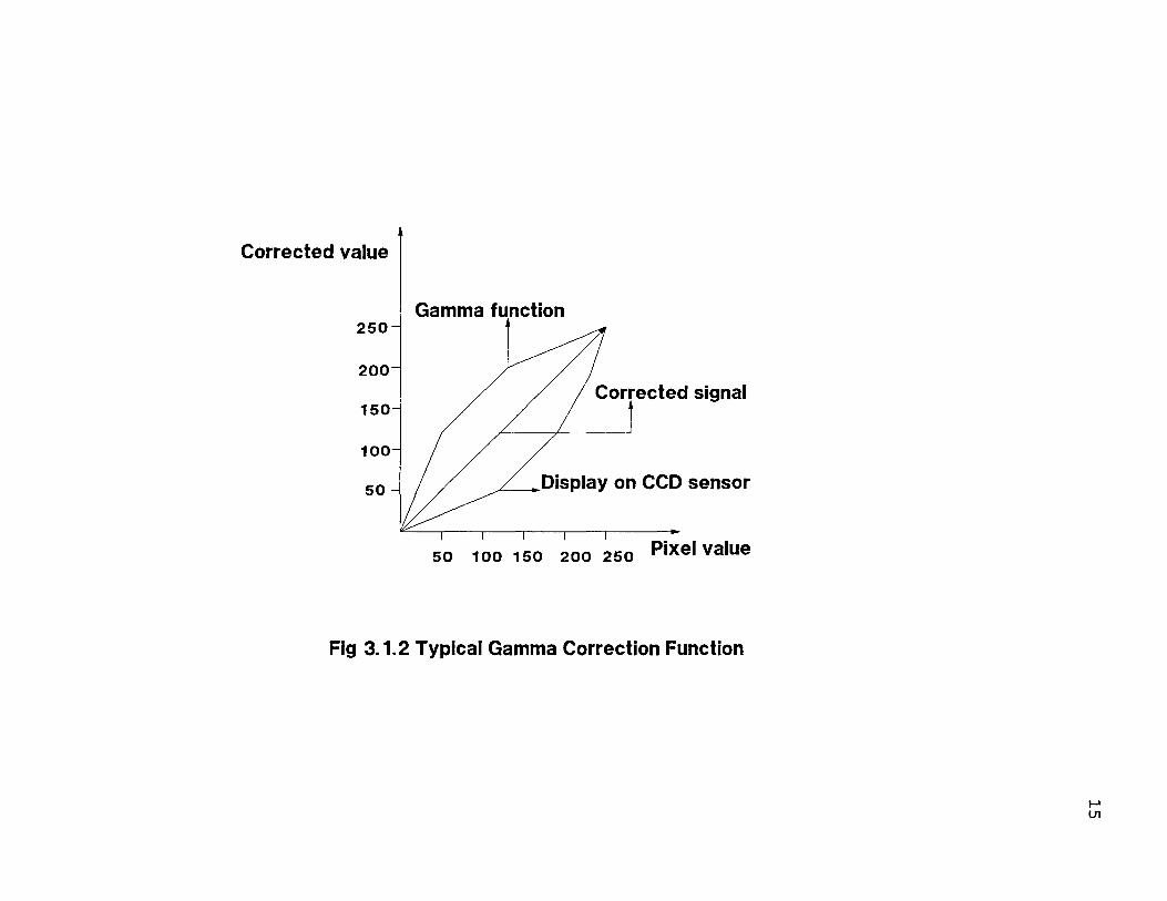
Fig 3.1.2 Typical Gamma Correction Function
15
16
Cr= (-44/256)R - (87/256)G + (131/256)B + 128
YCBCr-to-RGB conversion [2] :
R = Y + 1.370(Cr-128)
G = Y - 0.698(Cr-128) - 0.336(Cb-128)
B = Y + 1.730(Cb-128)
Raster to Block Conversion
In the encoding direction , the input data to the L64765 Color and Raster-Block converter
is in raster form consisting of horizontal scan lines of upto 8192 pixels. The L64765
converts the full image raster data into data blocks of eight pixels by eight pixels in raster
order, the format used by the downstream devices, the L64735 DCT Processor and the
L64745 JPEG Coder. Figure 3.1.3 shows how the first block on the display screen is
processed by the L64765.
In the encoding direction, the L64765 stores the eight complete scan lines in an
external strip memory. When the memory is filled, the L64765 begins reading data out of
the strip memory into the YCbCr buffer in 8 X 8 blocks. As each data value is read , a
new value is read , a new value is written into the strip memory at the same address. This
read-then-write operation reduces the amount of strip memory needed.
In the decoding direction, the L64765 reads in 8 X 8 blocks until a complete set
of eight scan lines is contained in the strip memory into the image area data reformatter
in raster order.
Data Interleaving
The data coming out of L64745 is initerleaved with all the components of a MCU
grouped together. Fig 3.1.4 and 3.1.5 show how the L64765 processes and outputs
interleaved data . The L64745 outputs four blocks of data per MCU : two blocks of
luminance data, followed by one block of Cb chrominance data followed by one block of
Cr chrominance data.
17
The number of blocks of each component in the input data stream is determined by the
L64745 internal parameters N0 through N3, which are set at the initialization. The
L64745 processes N0 blocks of component 0, followed by N1 blocks of component 1 ,
and so on. In applications using a complete JPEG chipset, No is set equal to 2, N1 and N2
are set equal to 1, and N3 is set to 0. Figure 3.1.6 shows the Block input ordering.
Quantization
Quantization categorizes data into the limited number of discrete values. Quantization is
a lossy process, meaning that information is lost in the quantization process . This loss is
called quantization noise.
The forward and inverse quantization functions performed by the L64745 JPEG coder
are given below. The data used in the quantization is stored within the L64745 in four
quantization tables. The symbols used are defined in the following the equations [5].
Forward Quantization:
Q(x(i),i) = round ( x(i)/q(i))
Inverse Quantization :
x'(i) = Q (x(i),i)*q(i)
where :
x(i) : DCT coefficient created by the L64735 DCT Processor
x'(i) : DCT coefficient generated by the L64745. Since the quantization
is a lossy process, x'(i) is not necessarily equal to x(i).
Q(x(i),i): Quantized DCT coefficient. Q(x(i),i) is the output of the quantizer
and the input to the coding modules when the L64745 is in the
DCT encoding configuration. Q(x(i),i) is the output of the
decoding modules and input to the inverse quantizer when the
L64745 is in DCT decoding configuration.
q(i): Quantization stepsize from the quantization table for the
component being quantized.
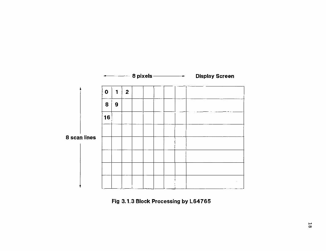
Fig 3.1.3 Block Processing by L64765
18
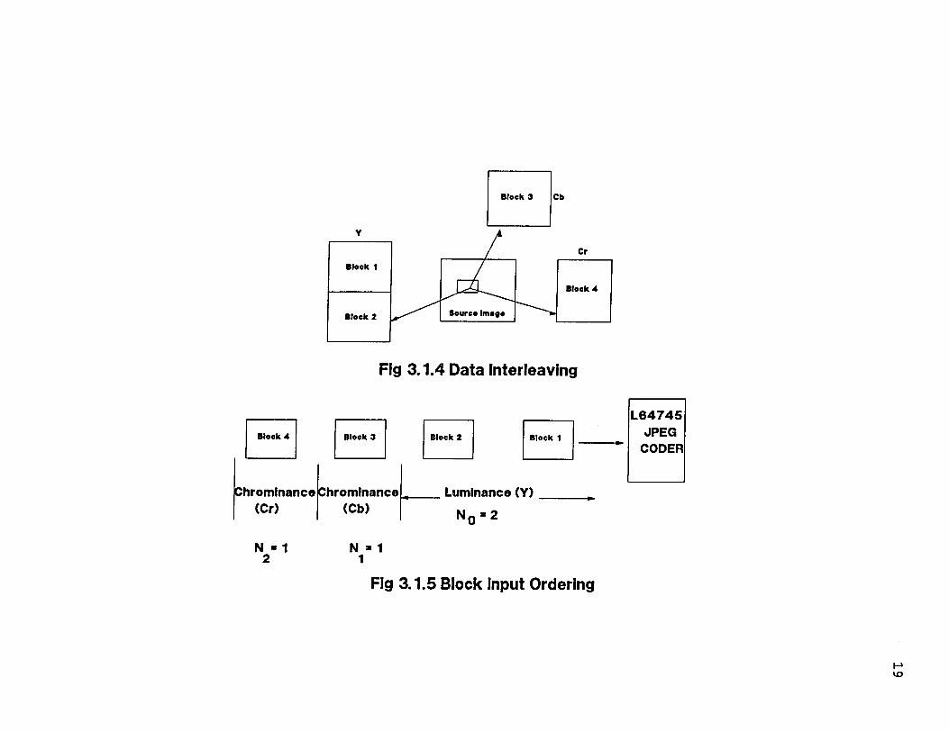
Fig 3.1.4 Data Interleaving
Fig 3.1.5 Block Input Ordering
19
20
round(x): Rounding function. Round(x) rounds to the nearest integer. When
x is half way between the 2 integers , round(x) rounds up for the
positive and down for negative values of x.
is Index of the DCT or receieved DCT coefficient. i is in the range
from 0 to 63 inclusive.
3.2 Typical System Application
Fig 3.2.1 gives the three components of the JPEG chipset in a typical video real-time
image processing application. This system design supports bidirectional data flow for
both encoding and decoding . The text following the figure describes the function of the
devices in the example.
In encoding applications, the A/D converter converts analog input RGB data into
24-bit digital RGB data as the input to the L64765.
The L64765 Color and Raster to Block converter converts RGB values to
luminance (Y) and chrominance(Cb,Cr) components and converts the raster image into
8 X 8 blocks in the compression direction. In the decompression direction, it converts
luminance and chrominance components into RGB and translates the 8 X 8 blocks into
full-screen raster signal.
The strip memory buffers eight scan lines of the raster-ordered image to assist in
the raster-to-block conversion in the L64765.
The L64735 DCT Processor performs a 2D discrete cosine transform on the 8 X 8
blocks to produce DCT coefficients.
The L64745 JPEG Coder quantizes and encodes the DCT coefficients into a
compressed data stream.
The Compressed Memory stores the compressed DCT coefficients. In real-time
video applications, 512 Kbytes of storage can store an average of 16 compressed images
of sizes 512 X 480 X 24 at a compression of 24 to 1.
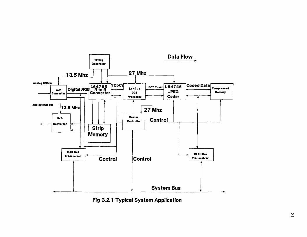
Fig 3.2.1 Typical System Application
21
22
The Master Controller provides the control signals and performs the handshaking
both between the host and the L64745, and also between the host and the Compressed
memory and the system bus.
The Timing Generator generates the horizontal and vertical synchronization
signals.
In the decoding case, the data flow is reversed, and the D/A Converter converts
the digital RGB image data from the L64765 into the analog RGB data.
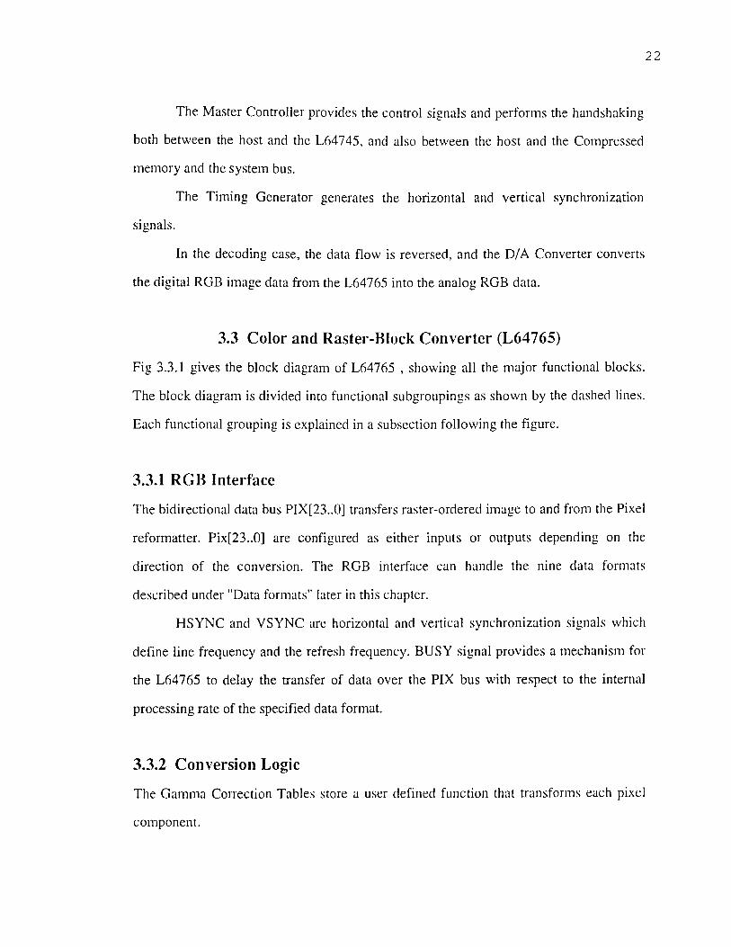
3.3 Color and Raster-Block Converter (L64765)
Fig 3.3.1 gives the block diagram of L64765 , showing all the major functional blocks.
The block diagram is divided into functional subgroupings as shown by the dashed lines.
Each functional grouping is explained in a subsection following the figure.
3.3.1 RGB Interface
The bidirectional data bus PIX[23..0] transfers raster-ordered image to and from the Pixel
reformatter. Pix[23..0] are configured as either inputs or outputs depending on the
direction of the conversion. The RGB interface can handle the nine data formats
described under "Data formats" later in this chapter.
HSYNC and VSYNC are horizontal and vertical synchronization signals which
define line frequency and the refresh frequency. BUSY signal provides a mechanism for
the L64765 to delay the transfer of data over the PIX bus with respect to the internal
processing rate of the specified data format.
3.3.2 Conversion Logic
The Gamma Correction Tables store a user defined function that transforms each pixel
component.
Fig 3.3.1 L64765 Logic Symbol
23
24
The L64745 has three such tables, and each table has 256 eight bit entries. These
tables can be read or written as described later in "Configuration and Control". The
Color Converter uses a digital matrix to perform the color conversion specified in CCIR
601 Recommendation, Mod F [2]. The color conversion matrix may be by-passed in
either direction to allow systems with images already in YCbCr space to use the raster to
block conversion feature. The data after color conversion must be in the correct range, a
Range Limiter clamps the data to the appropriate boundary value.
The Resampling Filters implement one of the two built in transfer functions,
depending on the direction of the conversion. The filters operate only on the chrominance
components Cb and Cr. In the encoding direction, downsampled image data is
downsampled (decimated). In the decoding direction, downsampled image data is
reconstructed (interpolated).
In the encoding direction, the Multiplexer combines the Chrominance
components in the data stream sent to the memory strip interface. In the decoding
direction, the Demultiplexer extracts Cr and Cb data into separate data streams for
conversion to RGB by the color converter.
3.3.3 Strip Memory Interface
An external strip memory stores the raster data to facilitate raster-block-conversion.
Since a 16 bit YCbCr pixel must be read and written every 74 nanoseconds at 13.5 MHz,
the 16- bit strip memory data bus cycle time is 37 nano seconds. Static RAMS with an
access time of 25 nanoseconds are typically used in the strip memory.
When the L64765 begins processing a raster-ordered image, the Strip Memory
Control places the starting address 0x0000 on ADDR[15:0] and signals a write operation
via MEM_RW. The L64765 then writes eight scan lines into the strip memory on
DATA[15:0], incrementing the address with each write. Once the strip memory is full,
25
the strip memory control reads the old strip out in block order while writing the new strip
into memory in Raster order. This operation is done on a pixel basis, reading a pixel out
before writing a new pixel into the strip memory . The Data Register buffers read and
write data .
The 16-bit address can access upto 64K pixels . This memory addressing range is
more than enough to support eight 17-inch scan lines at 300 dpi (40,800 pixels).
However, the system configuration need only include the amount of memory that will
actually be used. The L64765 requires the minimum amount of memory as defined in the
equation below, where M is the memory size in 16-bit words and width is the width of
the active window in MCUs.
M = 128 X width
For example , an image 512 pixels wide requires a strip memory of 4K (4096) 16 bit
words.
3.3.4 YCbCr Interface
The bidirectional data bus YCbCr[7:0] transfers converted data to and from the YCbCr
Buffer. During raster-block operation, the 8-bit wide bus passes pixel data organized in 8
X 8 blocks to and from the L64735 DCT processor. An optional Y-only format is
supported by forcing the Cr and Cb components to be black (0x80). This allows the
YCbCr interface to operate at the same rate regardless of the format.
Three signals specify the state of the YCbCr interface. BS indicates the start of a
block of 64 data samples. LBS indicates the end of last block of 64 data samples. The
L64765 asserts the FRQ signal to stop the flow of data out of the YCbCr bus during
encoding operations, or into the YCbCr bus during encoding operations, or into the
YCbCr bus during decoding operations.
26
3.3.5 Internal Registers
The address registers point to one of the registers in the Configuration Register File or to
an address in the Gamma Correction Tables. The Configuration Register File includes
five registers : Width, Height, WDelay, HDelay, and Control.
3.3.6 Control Signals
The Internal Register Control Logic accepts three inputs : READ* and WRITE* control
the direction of the access to the internal register addressed by R[1:0] and the contents of
the address registers. The output enable signal OE*, controls the output buffers for
signals PIX[23:0], HSYNC, VSYNC, DATA[15:0],YCbCr[7:0],LBS and BS. ( The
bidirectional buffers are not shown in the block diagram). CLK is the clock for all
internal registers and memory elements. The clock frequency is 27 MHz.
3.4 Configuration and Control
This section describes the configuration and initialization of the L64765. It also shows
functional waveforms for the read and write waveforms for the read and write operations.
3.4.1 Address Register
The initialization of address register is done in the following way :
Address Register Write:
- Set R[ 1 :0] to 00.
- Assert Write* LOW for at least the minimum pulse width. When WRITE* is
asserted , the L64765 holds the PIX[23:16] while WRITE* is asserted.
Place the new value on PIX[23:16] while WRITE* is asserted.
- The new value is stored in the address register on the rising edge of WRITE*.
Address Register Read :
Set R[1:0] to 00.

27
- Assert READ* LOW for at least the minimum pulse width. The L64765 places
the Address Register value on PIX[23:16] after the falling edge and holds it past
the rising edge of READ*.
Fig 3.4.1 gives the address read and write waveforms.
3.4.2 Gamma Correction Tables
The L64765 has three separate gamma correction tables, one each for the Red, Green ,
and Blue digital inputs. These are 256 entries for red, green, and blue. The Address
register points to a gamma correction table location when R[1:0] is set to 01. The data
written to a gamma address must be written in order: Red, Green, then Blue. Once the
Blue value has been written, the address Register automatically increments by one.
Gamma Table Write :
To write the gamma correction tables:
- Set the Address Register to the starting address of the write as described earlier in
the "Address Register".
- Set R[1:0] tool.
Assert Write* for at least the minimum pulse width.
Place the Red value on PIX[23:16] while WRITE* is asserted.
The value is written into the Red gamma table on the rising edge of the WRITE*.
- Write the Green value in the same way as Red.
- Write the Blue value in the same way as Red.
- Once the Blue value is written , the address register automatically
increments by one.
Repeat the steps 3, 4, 5 to write successive values into the gamma table.
For reading the written value the same procedure is followed, but instead of WRITE*
signal READ* is used and instead of placing the values on the PIX bus , the chip places
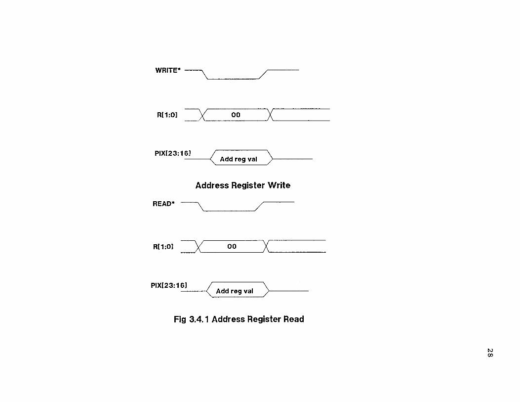
Fig 3.4.1 Address Register Read
28
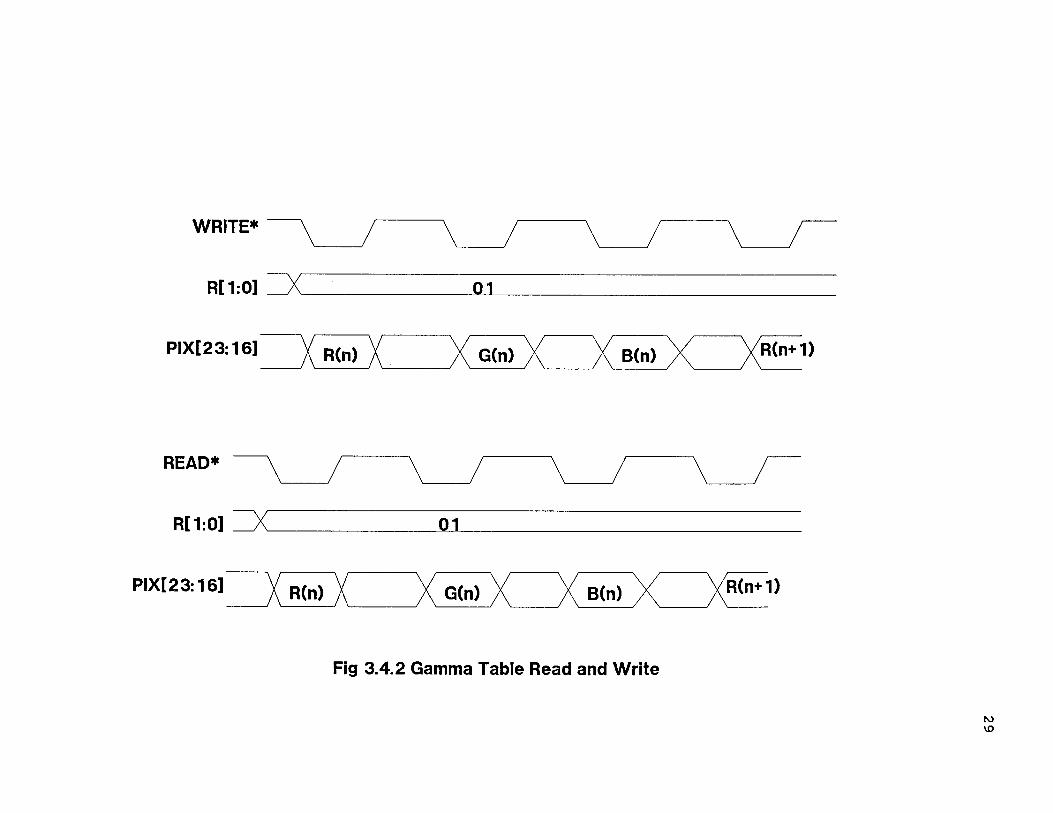
Fig 3.4.2 Gamma Table Read and Write
29
30
the values itself on the PIX bus at the rising edge of READ*. Figure 3.4.2 shows the
write and read operations for Gamma Tables.
3.4.3 Configuration Registers
L64765 contains five internal configuration registers. The eight-bit Control Registers set
the data format of the input RGB data on the PIX bus and controls the other aspects of
operation.
The Configuration registers are addressed in the same manner as the gamma
correction tables. For all registers except the Control register, two write operations are
required to write the full contents of the register. The least significant byte is written first
to the address shown in Table 3.4.1 and the most significant byte is written to the next
higher address. Only the four least significant bits of the Address Register are used to
address the configuration registers.
The registers are written and read in the same manner as for gamma correction
tables, with R[1:0] set to 10.
Control Register
The Control Register is accessed by setting the bit 3 of Address Register to 1 and R[1:0]
to 10. Figure 3.4.3 shows the content of the Control Register.
1) Go Control (GO)
Go enables the L64765 to begin processing the data at the next rising edge of VSYNC.
After GO is set , it can only be cleared by resetting the L64765. The L64765 is reset by a
write operation with R[1:0] set to 11.
2) Output Enable Control (OEN)
OEN and control input OE* work together to enable and disable the state of all
bidirectional signals. When either OEN is set to HIGH or OE* is deasserted (HIGH), the
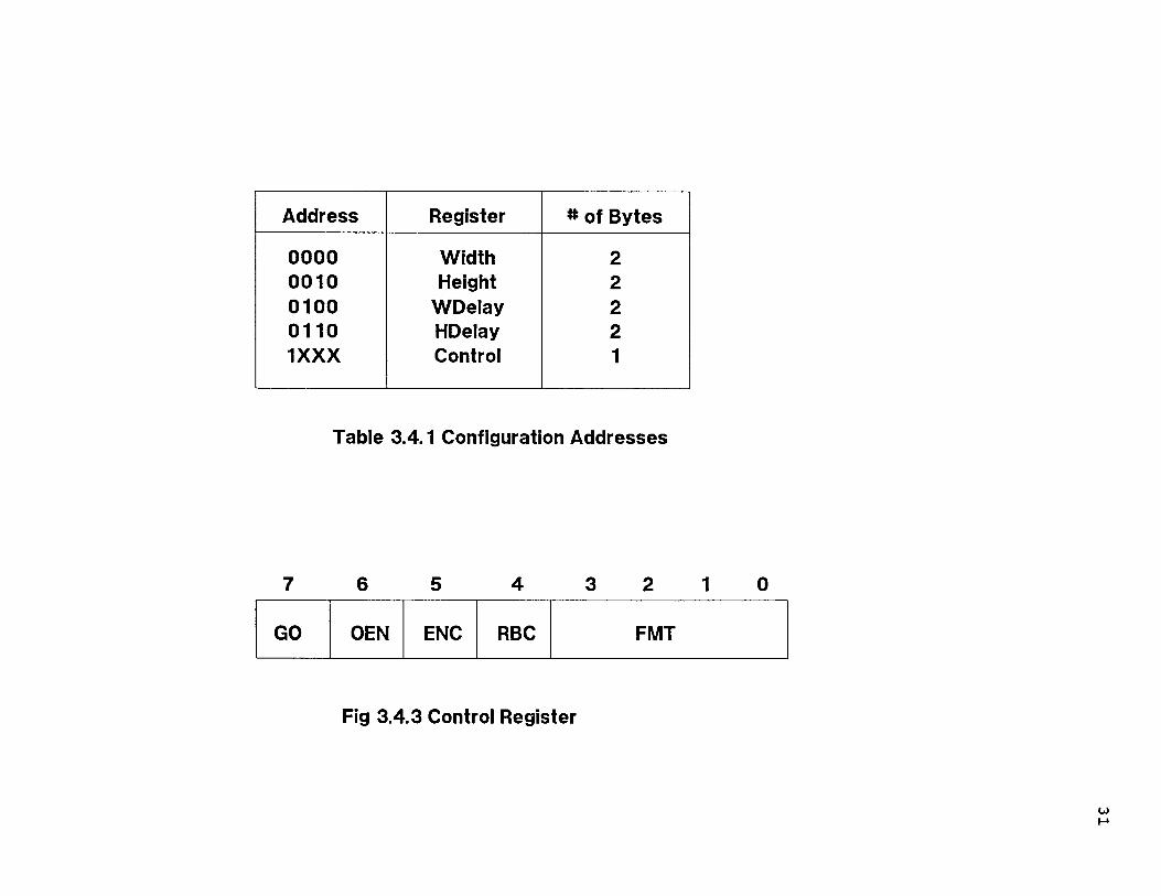
Table 3.4.1 Configuration Addresses
Fig 3.4.3 Control Register
31
32
bidirectional signals are held in the high impedance state. For these signals to be enabled,
OEN must be set to zero and OE* set to zero.
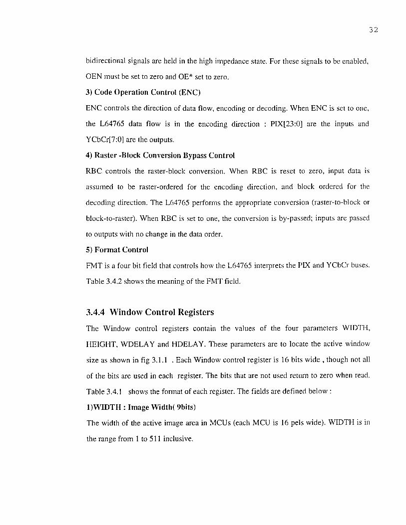
3) Code Operation Control (ENC)
ENC controls the direction of data flow, encoding or decoding. When ENC is set to one,
the L64765 data flow is in the encoding direction : PIX[23:0] are the inputs and
YCbCr[7:0] are the outputs.
4) Raster -Block Conversion Bypass Control
RBC controls the raster-block conversion. When RBC is reset to zero, input data is
assumed to be raster-ordered for the encoding direction, and block ordered for the
decoding direction. The L64765 performs the appropriate conversion (raster-to-block or
block-to-raster). When RBC is set to one, the conversion is by-passed; inputs are passed
to outputs with no change in the data order.
5) Format Control
FMT is a four bit field that controls how the L64765 interprets the PIX and YCbCr buses.
Table 3.4.2 shows the meaning of the FMT field.
3.4.4 Window Control Registers
The Window control registers contain the values of the four parameters WIDTH,
HEIGHT, WDELAY and HDELAY. These parameters are to locate the active window
size as shown in fig 3.1.1 . Each Window control register is 16 bits wide , though not all
of the bits are used in each register. The bits that are not used return to zero when read.
Table 3.4.1 shows the format of each register. The fields are defined below :
1)WIDTH : Image Width( 9bits)
The width of the active image area in MCUs (each MCU is 16 pets wide). WIDTH is in
the range from 1 to 511 inclusive.
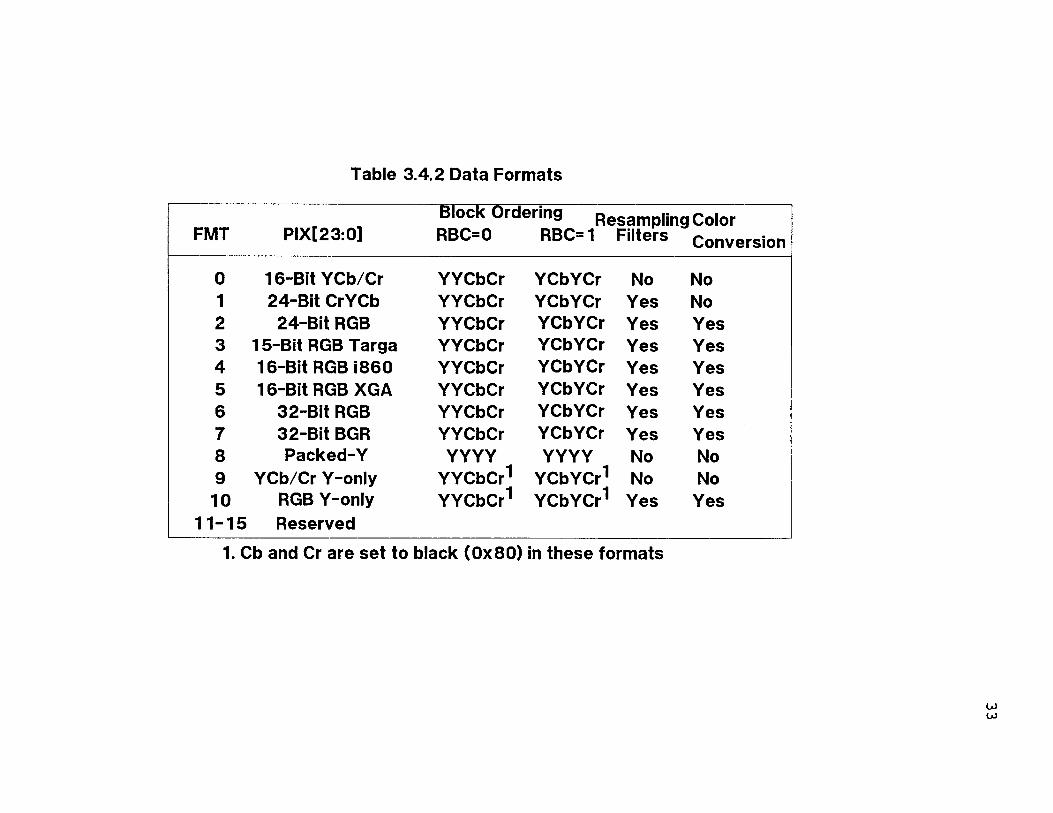
Table 3.4.2 Data Formats
1. Cb and Cr are set to black (0x80) in these formats
33
34
2)HEIGHT : Image Height (10 bits)
The height of the active image area in MCUs (each MCU is 8 pixels high). HEIGHT is in
the range of 2 to 2023 inclusive.
3)WDELAY : Width delay (13 bits)
The delay in pixels from the start of the scan line to the first active pixel. The rising edge
of HSYNC indicates the start of the scan line. WDELAY is in the range of 0 to 8191
inclusive.
4)HDELAY : Height delay (13 bits)
The delay in scan lines from the start of the frame to the first active scan line . The rising
edge of VSYNC indicates the start of the frame. HDELAY is in the range of 0 to 8191
inclusive.
3.5 Reset Operation
A write operation to the Reset Register performs a reset operation on the L64765 and the
value written is ignored. A reset operation clears the Go bit in the Control register but
does not otherwise affect the state of L64765 . The contents of the gamma correction
tables and the configuration registers are unchanged by a reset operation. A reset
operation also sets the FRQ output to LOW, thus allowing the system clock to reach the
L64735 and L64745. Figure 3.5.1 shows the waveforms for the reset operation.
3.6 Initialization Sequence
When the L64765 is powered on, the contents of the internal registers are undefined .
Before the device is put into operation, this initialization sequence should be performed:
1) Reset the L64765 as described under "Reset". Resetting clears the Go bit.
2) Set the values of WIDTH, HEIGHT, WDELAY, and HDELAY as described under
"Window Control Registers".
35
3) Set the values of the operating parameters in the Control Register but do not set the Go
bit yet.
4) Load the values into the Gamma Correction Tables as described earlier.
5) Reset the L64765 again.
6) Reset the L64735 DCT Processor and the L64745 Coder.
7) Set the Go bit. The L64765 is now ready for operation.
3.7 L64735 DCT Processor
The L64735 DCT Processor had four basic functional configurations:
• Signed forward DCT
• Signed inverse DCT
• Unsigned forward DCT
• Unsigned inverse DCT
During initialization, the L64735 is programmed for one of these four functional
configurations. Input signals UNSIGNED, FORWARD, ORDERZZ, and BYPASS
control the functional configuration and operation of the L64735.
Each of the basic functional configurations is illustrated with a block diagram and
described briefly in this section.
3.7.1 Signed Forward DCT
For this configuration, Forward is HIGH and UNSIGNED is held LOW. Figure 3.7.1
shows the signed forward DCT configuration.
The L64735 receives nine-bit pixel data from the L64765 Color and Raster-Block
Converter on PIX[8:0]. The L64765 organizes the pixel data in 8X8 blocks . Input signal
PBS indicates the start of a pixel block. The DCT Transform computes the 12-bit DCT
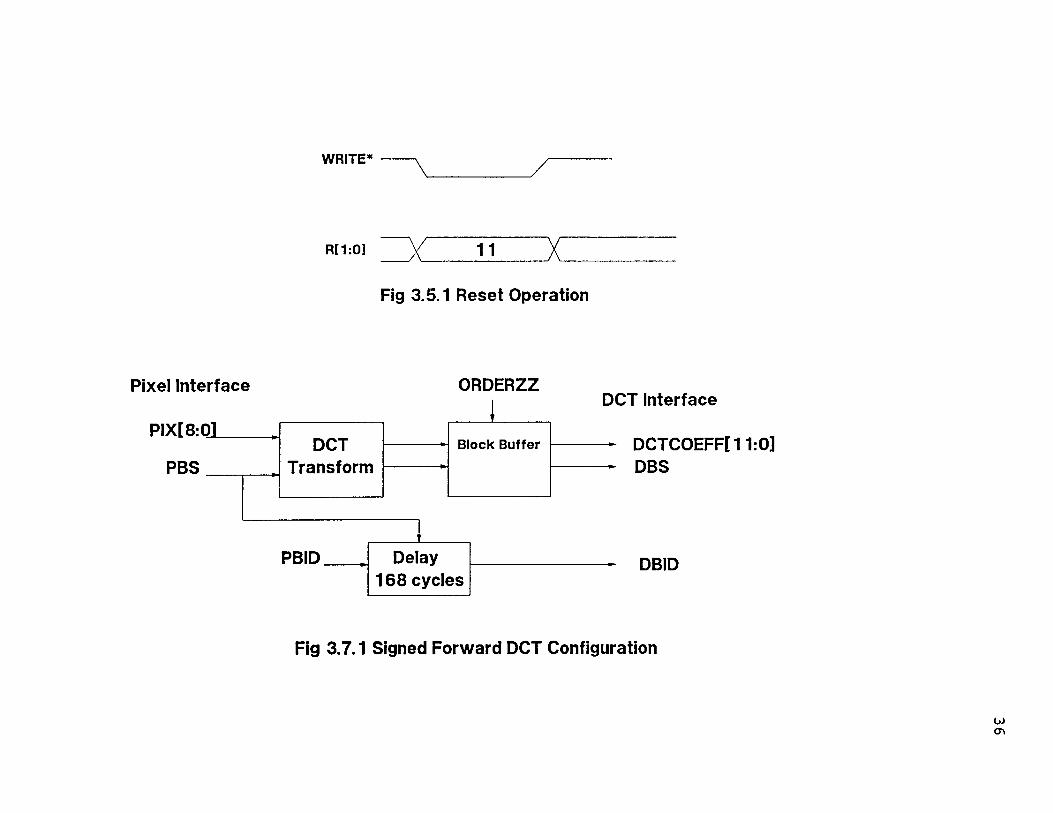
Fig 3.5.1 Reset Operation
Fig 3.7.1 Signed Forward DCT Configuration
36
37
coefficients for the block.The Block Buffer assembles the DCT coefficients in either
raster or zig zag order , depending on the state of the input signal ORDERZZ. The 8 X 8
block appears on the DCTCOEFF[ 1 1:0] with a delay of 168 cycles. DBS indicates the
start of a block of DCT coefficients.
3.7.2 Signed Inverse DCT
Fig 3.7.2 shows the signed inverse DCT configuration. For this, FORWARD is held
LOW and UNSIGNED is held LOW. The LBS signal produced by the L64745 is
propagated to PBID and drives the L64765 LBS input. The internal organization is
similar to the Signed Forward DCT, with DCT and DBID flowing in the opposite
direction. The IDCT Transform reconstructs the pixel data from the DCT coefficients.
3.7.3 Unsigned Forward and Inverse DCT
Figures 3.7.3 and 3.7.4 shows the unsigned forward and inverse DCT configurations
respectively.
Differences from signed data configurations are:
. PIX data is eight-bits wide (PIX 0 is not used).
. DCTCOEFF data is 11 bits wide (DCTCOEFF:0 is not used)
. PIX data is level shifted by the ADDER ( shown as the circle with the plus sign).
3.7.4 Signal Descriptions
The external Interface to the L64735 is shown in the figure
Pixel Interface Signals:
PIX[8:0] (Pixel data bus)
Pix[8:0] comprise the pixel data bus . When the L64735 is operating in the forward
direction, PIX[8:0] are inputs for the 8 X 8 blocks of image data sent by
the L64765 . When the L64735 is operating in the inverse direction, PIX[8:0] are the
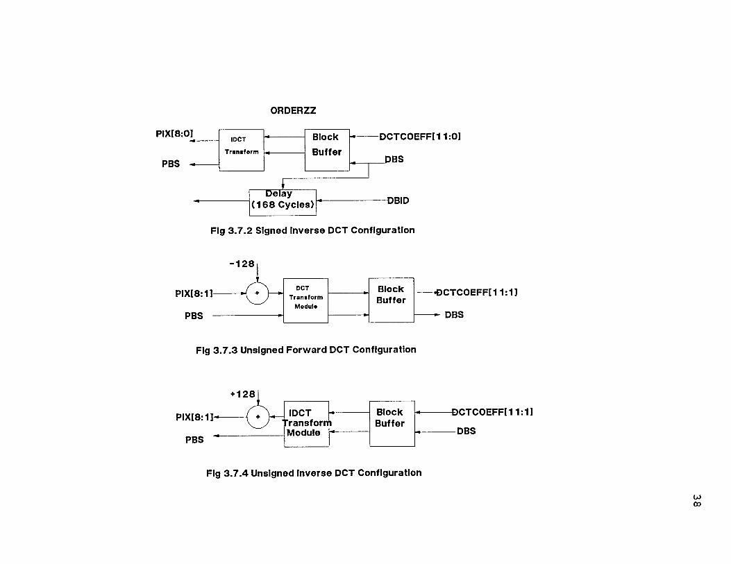
Fig 3.7.2 Signed Inverse DCT Configuration
Fig 3.7.3 Unsigned Forward DCT Configuration
Fig 3.7.4 Unsigned inverse DCT Configuration
38
39
outputs for the blocks of reconstructed data sent to the L64765. When the L64735 is
configured for the unsigned data PIX:0 is not used.
PBS (Pixel Block Start)
PBS is asserted HIGH coincident with the first data sample in each block of the pixel
data on PIX[8:0]. PBS is an input for forward DCT operation and output for inverse DCT
operation.
PBID (Pixel Block ID)
PBID is connected to DBID through a 168-cycle delay. PBID is only sampled when PBS
or DBS is asserted HIGH or an integer multiple of 64 cycles after PBS or DBS was last
asserted. PBID is an input for forward operation and an output for inverse operation.
DCT Interface Signals : These signals comprise of the interface to the L64745 JPEG
Coder.
DCTCOEFF[11:0] (DCT Coefficient Bus)
DCTCOEFF[11:0] are outputs in the forward direction, and inputs for the compressed
data in the inverse direction. When the L64735 is configured for Unsigned data,
DCTCOEFF.0 is not used.
DBS ( Data Block Start)
DBS is asserted HIGH coincident with the first sample data in each block of pixel data on
the DCTCOEFF bus. DBS is an output for the forward operation and an input for inverse
operation.
DBID ( DCTCOEFF Block ID)
DBID is connected to the PBID through a 168-cycle delay. PBID is only sampled when
the DBS is asserted HIGH or an integer multiple of 64 cycles after DBS was last asserted.
DBID is an input for the forward operation and an input for the inverse operation.
40
3.8 Configuration and Control
Four input signals, BYPASS, FORWARD, ORDERZZ, and UNSIGNED control the
function of the L64735 and the format of the DCTCOEFF and PD( buses. Table 3.8.1
summarizes the configuration and control signals. To prevent data loss configuration
inputs must not be changed until at least 168 clock cycles after the last input value has
been received by L64735.
3.9 L64745 Operation Modes
This section discusses and illustrates the following functions of L64735:
• Forward DCT Operation
• Inverse DCT Operation
• By-pass Operation
3.9.1 Forward DCT Operation
Fig 3.9.1 shows the input and output waveforms for the forward DCT Operation. The
figure assumes the block ordering of data, ORDERZZ, is held HIGH for zig zag ordering.
The ordered pair notation for the PIX and DCTCOEFF buses give the location of the data
word in the 8 X 8 block in (x,y) coordinates. Output data words appear contiguously
synchronized with the system clock after a delay of 168 clock cycles.
3.9.2 Inverse DCT Operation
Fig 3.9.2 shows the input and output waveforms for inverse DCT Operation. The figure
assumes block ordering of the input , ORDERZZ, is held HIGH for zig-zag ordering.
Output data words again appear contiguously synchronized with the system clock after a
delay of 168 clock cycles.
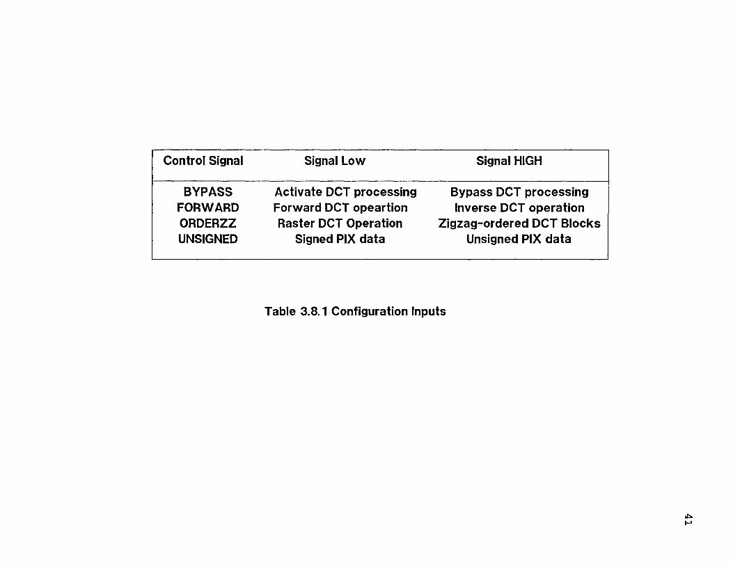
Table 3.8.1 Configuration Inputs
41
42
3.9.3 Bypass Operation
Fig 3.9.3 shows the waveforms for data transfer in the forward direction with BY-PASS
asserted HIGH. During Bypass operation, PBS and DBS are not used and their state is
undefined
3.10 JPEG Coder (L64745)
This section describes the functioning of the L64745 which is the actual encoder and
decoder chip.
3.10.1 Signal Description
The external Interface to the L64745 consists of the signals shown in the Fig 3.10.1 .
Each of the signal is explained below.
DCTCOEFF[10:0]
DCTCOEFF[10:0] carries the DCT coefficients. It is an I/O bus. When the L64745 is
configured as an encoder, DCTCOEFF[10:0] are inputs from DCT Processor. When
L64745 is operating as a decoder these form the outputs for the reconstructed DCT
coefficients.
BS (Block Start)
BS is asserted HIGH coincident with the first data sample in each block of the DCT
coefficients on DCTCOEFF[20:0]. BS is an input for encoder operation and an output for
decoder operation.
LBS (Last Block Strobe)
LBS is asserted HIGH following the last data sample of the last block in the image on
DCTCOEFF[10:0]. LBS is an input for encoder configurations and an output for decoder
configurations.
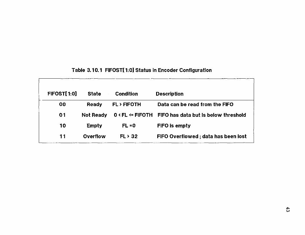
Table 3.10.1 FIFOST[1:0] Status in Encoder Configuration
FIFOST[1:0] State Condition Description
00 Ready FL > FIFOTH Data can be read from the FIFO
01 Not Ready 0 < FL <= FIFOTH FIFO has data but is below threshold
10 Empty FL =0 FIFO is empty
11 Overflow FL > 32 FIFO Overflowed ; data has been lost
43
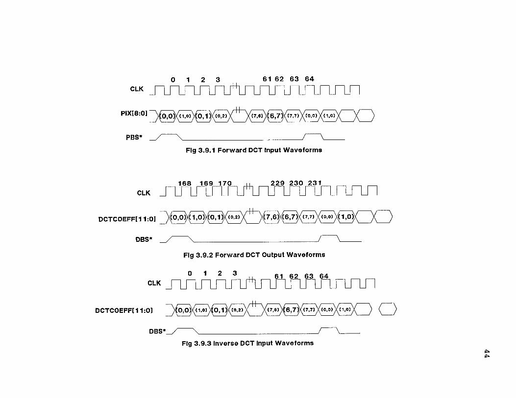
Fig 3.9.1 Forward DCT Input Waveforms
Fig 3.9.2 Forward DCT Output Waveforms
Fig 3.9.3 Inverse DCT Input Waveforms 44
45
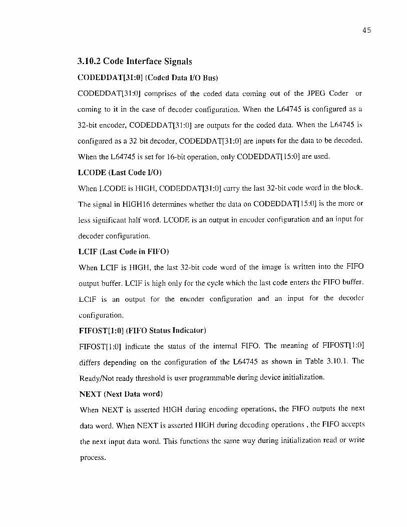
3.10.2 Code Interface Signals
CODEDDAT[31:0] (Coded Data I/O Bus)
CODEDDAT[31:0] comprises of the coded data coming out of the JPEG Coder or
coming to it in the case of decoder configuration. When the L64745 is configured as a
32-bit encoder, CODEDDAT[31:0] are outputs for the coded data. When the L64745 is
configured as a 32 bit decoder, CODEDDAT[31:0] are inputs for the data to be decoded.
When the L64745 is set for 16-bit operation, only CODEDDAT[15:0] are used.
LCODE (Last Code I/O)
When LCODE is HIGH, CODEDDAT[31:0] carry the last 32-bit code word in the block.
The signal in HIGH16 determines whether the data on CODEDDAT[15:0] is the more or
less significant half word. LCODE is an output in encoder configuration and an input for
decoder configuration.
LCIF (Last Code in FIFO)
When LCIF is HIGH, the last 32-bit code word of the image is written into the FIFO
output buffer. LCIF is high only for the cycle which the last code enters the FIFO buffer.
LCIF is an output for the encoder configuration and an input for the decoder
configuration.
FIFOST[1:0] (FIFO Status Indicator)
FIFOST[1:0] indicate the status of the internal FIFO. The meaning of FIFOST[1:0]
differs depending on the configuration of the L64745 as shown in Table 3.10.1. The
Ready/Not ready threshold is user programmable during device initialization.
NEXT (Next Data word)
When NEXT is asserted HIGH during encoding operations, the FIFO outputs the next
data word. When NEXT is asserted HIGH during decoding operations , the FIFO accepts
the next input data word. This functions the same way during initialization read or write
process.
46
3.10.3 Control Signals
These input signals control the initialization and certain operational aspects of the
L64745.
HIGH16 (Half word Location)
HIGH16 is only meaningful when the L64745 is set for 16-bit operation. When this is
asserted the CODEDDAT[ 15:0] is the more significant 16-bit half word of the 32-bit
coded data word. When HIGH16 is deasserted , CODEDDAT[15:0] is the less significant
16-bit half word. For 32 bit operation HIGH16 must be deasserted LOW.
INIT (Initialization)
When INIT is asserted (HIGH), the L64745 operating parameters can be read and written
as described in "Device Initialization". When the INIT is deasserted (LOW), the L64745
functions as configured by bits STAT,LL, and ENC bits in the Configuration Group.
RW (Read/Write Select)
RW is used only during device initialization. When RW is HIGH, the device parameters,
code tables, and quantization tables can be read on the CODEDDAT bus. When the RW
is low, the parameters and tables can be written from the CODEDDAT bus.
Reset (Device Reset)
RESET resets the L64745. Resetting the L64745 prepares it to process new image frame..
To reset, RESET must be asserted (HIGH) for at least 2 clock cycles and deasserted for
at least four clock cycles after device initialization. Resetting the L64745 clears the FIFO
buffer but does not affect the contents of the quantization or code tables.
CLK (System Clock)
CLK is the system clock that controls the internal state of the L64745. All input signals
to the L64745 are sampled at the rising edge of CLK.
47
OEN (Output Enable)
When OEN is HIGH, DCTCOEFF[10:0], CODEDDAT[31:01, LBS, LCODE, and BS are
enabled. When OEN is LOW, these signals are put in HIGH impedance state and the
internal memory elements are put in a low power state.
3.11 Configuration and Control
Internal data is written to and read from the L64745 during the initialization sequence via
the CODEDDAT bus. The internal data includes the functional configuration, operational
parameters, quantization tables, and code tables.
Input signals INIT and RW control the start and type of initialization
sequence(read or write). The initialization sequence begins when INIT is HIGH. RW is
HIGH for read and LOW for write sequences.
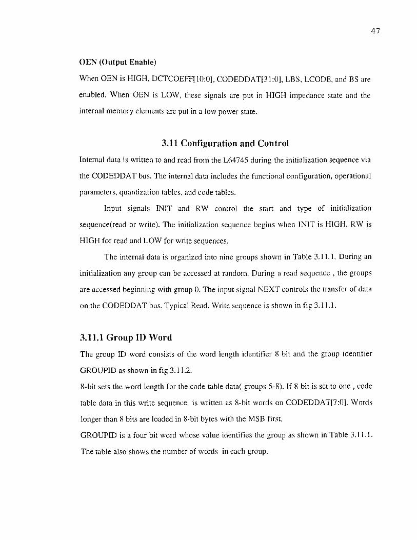
The internal data is organized into nine groups shown in Table 3.11.1. During an
initialization any group can be accessed at random. During a read sequence , the groups
are accessed beginning with group 0. The input signal NEXT controls the transfer of data
on the CODEDDAT bus. Typical Read, Write sequence is shown in fig 3.11.1.
3.11.1 Group ID Word
The group ID word consists of the word length identifier 8 bit and the group identifier
GROUPID as shown in fig 3.11.2.
8-bit sets the word length for the code table data( groups 5-8). If 8 bit is set to one , code
table data in this write sequence is written as 8-bit words on CODEDDAT[7:0]. Words
longer than 8 bits are loaded in 8-bit bytes with the MSB first.
GROUPID is a four bit word whose value identifies the group as shown in Table 3.11.1.
The table also shows the number of words in each group.
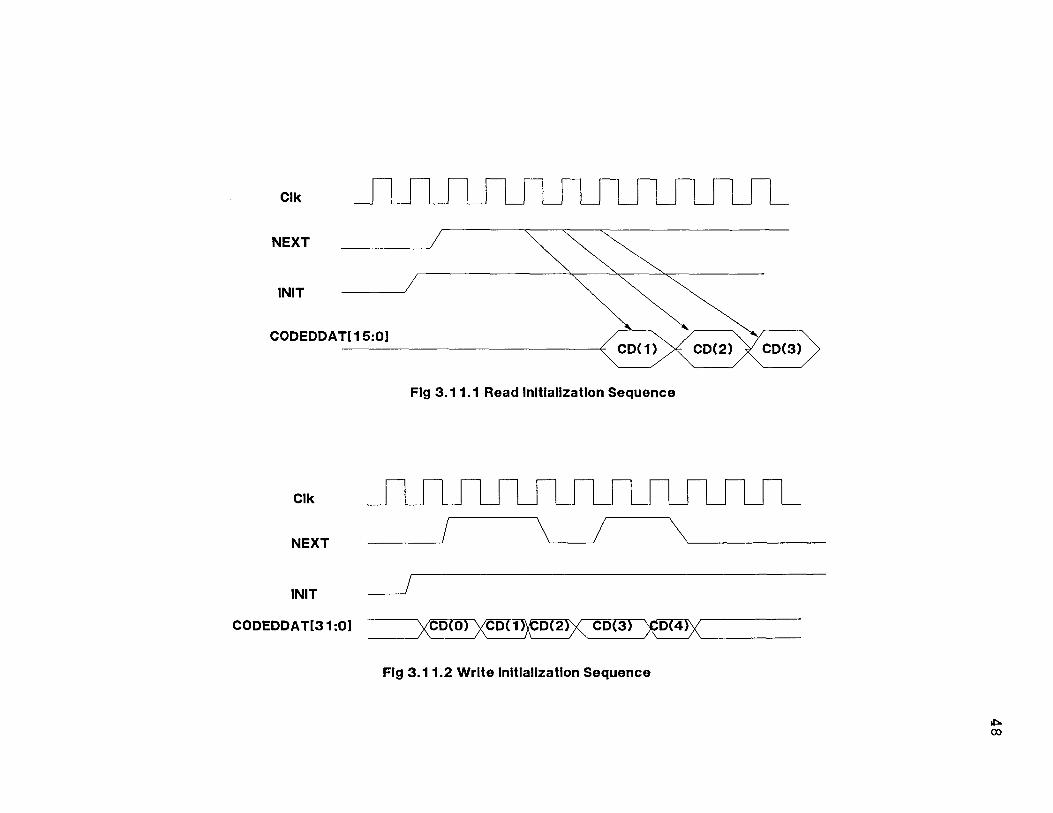
Fig 3.11.1 Read initialization Sequence
Fig 3.11.2 Write initialization Sequence
48
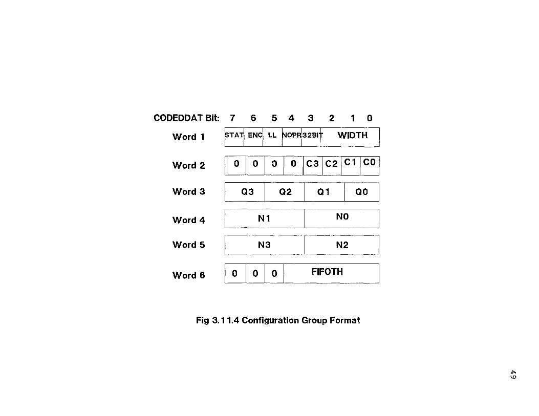
Fig 3.11.4 Configuration Group Format
49
50
Configuration Group
The Configuration Group must be written as the first step in the initialization sequence.
This group consists of six 8-bit control words. The data must be written in the order of
word 1 through word 6 as shown in Fig 3.11.2.
1) STAT (Statistics Configuration Selector)
When STAT is set to one, the L64745 is in statistics mode else it is in one of the
configurations set by ENC and LL.
2) ENC (Coder Configuration Selector)
When ENC is set to 1, the L64745 functions as an encoder. When ENC is set to 0, the
L64745 functions as a decoder.
3) LL (Lossless Configuration Selector)
When LL is set to 1, the L64745 functions as a lossless encoder. When ENC is set to 0,
the L64745 performs DCT-based coding.
4) NOPR (Internal Predictor Control)
When NOPR is set to 1, the internal predictor is disabled else it is used.
5) 32BIT (CODEDDAT Bus Width Selector)
When this is set to one , the full 32 bits of the coded data bus,CODEDDAT[31:0] are
used else only the lower 16 bits are used. When the L64745 is set to STAT mode (STAT
set to one), the lower 13 bits of the bus, CODEDDAT[12:0], are used.
6) WIDTH (Input data Width )
WIDTH is a 3-bit field whose value sets the width of the input data word in lossless
coding configuration. Bit 2 is the most significant bit. The number of bits in the input
data word is WIDTH + 4. The possible value ranges from 4 to 10 bits. WIDTH set 111 is
undefined and should not be used.
51
7) C3-CO (Code Table Selectors)
C3-CO select the code table to be used for each of the four components 3-0. When Cn is
set to 1, code table 1 is used for the nth component. When Cn is set to 0 , code table 0 is
used.
8) Q3-Q0 (Quantization Table Selectors)
Q3 through Q0 are 2 bit fields that select the quantization table to be used for each of the
four components 3-0. Each Qn selects one of the four quantization tables.
9) N3-N0 (Composite Sampling Ratio Selectors)
N3-NO are 4 bit fields that select the composite sampling ratio to be used for each of the
four components 3-0. A value of 0 indicates that the component is not used.
10) FIFOTH (FIFO threshold)
FIFOTH is a five-bit field whose value is the threshold for the Ready and Not Ready
state in the FIFO status report, FIFOST[1:0]. The value of FIFOTH is in the range from 0
to 31.
11) 0 (Zero value)
Bits marked with 0 in fig 4.14 must be written zero, and should be ignored when read.
3.12 Hardware description
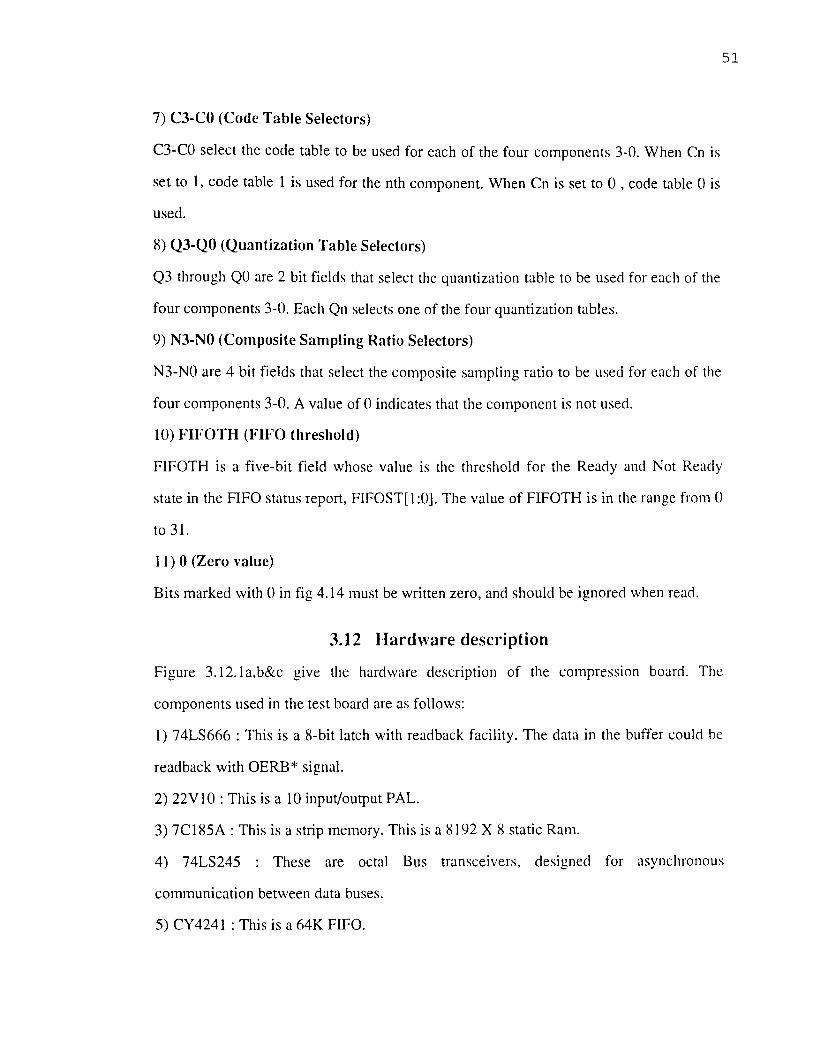
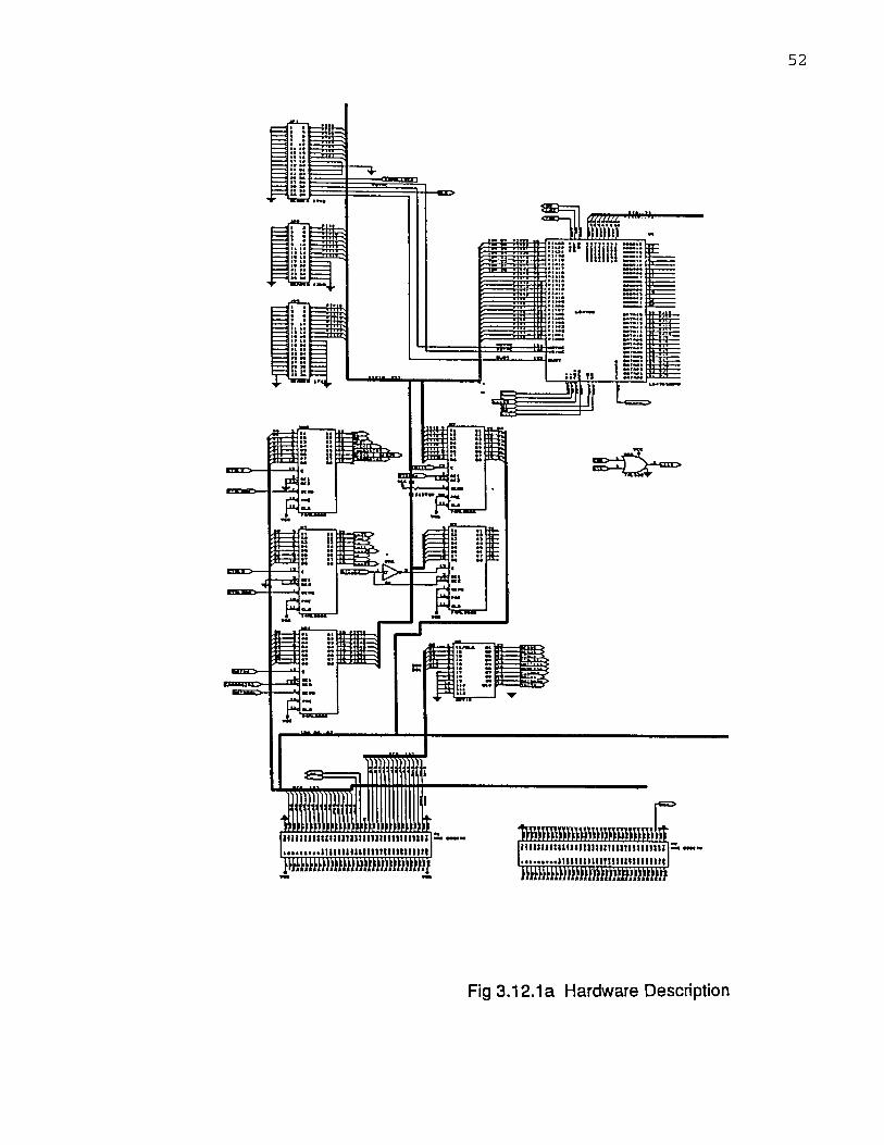
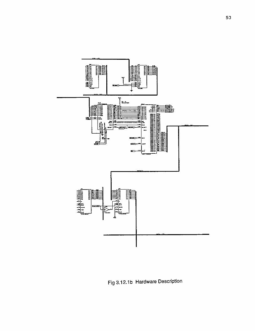
Figure 3.12.1a,b&c give the hardware description of the compression board. The
components used in the test board are as follows:
1) 74LS666 : This is a 8-bit latch with readback facility. The data in the buffer could be
readback with OERB* signal.
2) 22V10 : This is a 10 input/output PAL.
3) 7C185A : This is a strip memory. This is a 8192 X 8 static Ram.
4) 74LS245 : These are octal Bus transceivers, designed for asynchronous
communication between data buses.
5) CY4241 : This is a 64K FIFO.
52
Fig 3.12.1a Hardware Description
53
Fig 3.12.1b Hardware Description
54
Fig 3.12.1c Hardware Description
55
3.12.1 Operation
The operation of the circuit is explained here. The address and the data to the L64765 R
to B Converter is written through U21. This controls the initialization of the chip along
with the control registers U7 and U20. The PAL U8 supplies the necessary control
signals. U2 and U3 form the strip memory which enables the Raster to Block, or vice
versa conversion.
U9 supplies the initialization data to the Coder chip U13. The coded data from the
Coder chip is stored in the FIFOs until decompression.
The R to B converter gets the RGB or YUV data and does the necessary
conversion ie,0 raster to block or vice versa. DCT processor performs the DCT on these
blocks of data and passes them to the Coder chip which performs Huffman coding on the
DCT values obtained.
56
Chapter 4
MPEG STANDARD
4.1 MPEG Overview
MPEG stands for Moving Pictures Experts Group Committee. This International
Standard specifies the "Coding of Moving Pictures and Associated Audio for Digital
Storage Media at upto 1.5 Mbps" [1]. The standard is ISO 11172 for which the acronym
is MPEG.
The MPEG standard was developed in response to industry needs for an efficient
way of storing and retrieving video information on digital storage media (DSM). An
inexpensive medium was CD-Rom which could deliver data rates upto 1.2Mbps, and the
MPEG standard was accordingly aimed at approximately at this data rate. The committee
was instructed to develop a standard for data rates upto 1.5Mbps, and it was finally
decided that the MPEG decoders should be able to handle all data rates upto 1.856 Mbps.
This odd looking number was obtained by taking a telecommunications channel
bandwidth of 1984 kbps and subtracting 128kbps as an allowance for audio. The standard
allows much higher data rates to be specified, but it is expected that not all decoders will
be able to handle such higher data rates.
Two other relevant international standards were being developed prior to the
MPEG studies : H.261 by CCITT aimed at video-conferencing applications, and ISO
10918 by the ISO JPEG committee aimed at coding still pictures. Elements of both of
these standards were incorporated into the MPEG standard, but subsequent development
work by the committee resulted in coding elements found in neither.
ISO11172 specifies the bitstream in such a way that it is fairly straight forward to
design a conforming decoder. Decoders may differ considerably in architectural and
implementation details , but they have very few choices during the decoding process : the
methods and the results of the decoding process are closely specified by the ISO 11172.
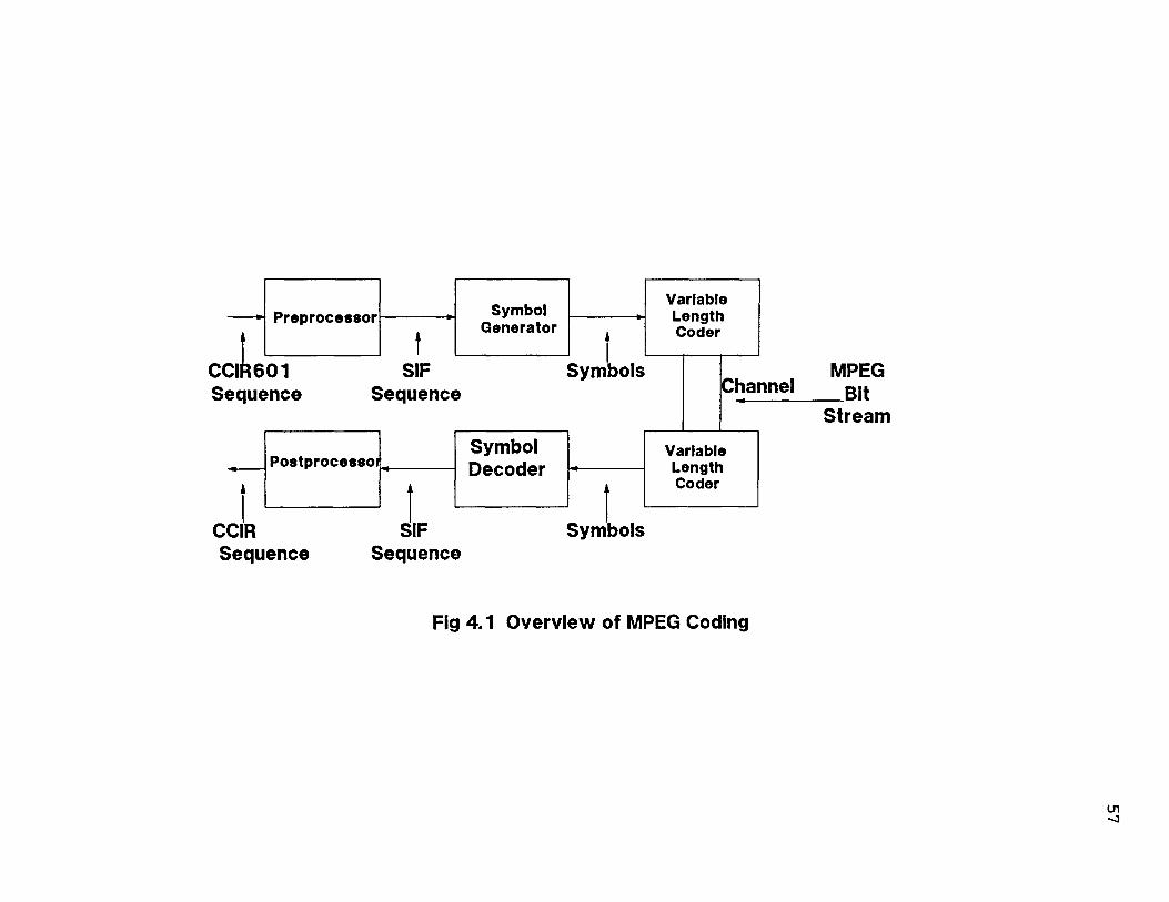
Fig 4.1 Overview of MPEG Coding
57
58
Decoders do have some freedom in methods of post processing and display, but the
results of such post processing cannot be used in subsequent decoding steps.
The situation is quite different for encoders. The encoders can make many
choices as they encode a picture: what quantization level to use , what block type to use,
what coding pattern to use, and so on.
4.2 Basic Concepts
The MPEG standard defines a format for compressed digital video [1]. Although the
MPEG standard is quite flexible, the basic algorithms have been tuned to work well at
data rates of about 1 to 1.5 Mbps, at spatial resolutions of about 350 pels horizontally by
250 pels vertically, and picture rates of about 24 to 30 frames per second. The use of the
word "picture" as opposed to "frame" is deliberate. MPEG codes progressively scans the
images and do not recognize the concept of interlace. Television frames are interlaced,
each frame is scanned twice with the scanning line offset by half a line in vertical
direction. Each scan produces a field containing half the scan lines of a full frame. Each
progressively scanned picture contains all the scan lines. Interlaced source video must be
converted to a non-interlaced format before coding. After decoding , the decoder may
optionally convert to an interlaced format before displaying the video.
The format of the coded video allows forward play and pause. Typical coding
methods allow random access and fast forward. Decoders can be built which permit
reverse play.
Compression of the digitized video comes from the use of several techniques :
subsampling of the chroma information to match the human visual system ( Human
vision is not very much perceptible to chroma information as luma information),
differential coding to exploit spatial redundancy, motion compensation (MC) to exploit
temporal redundancy, discrete cosine transform (DCT) to match typical image statistics,
uantization, variable length coding (VLC), and use of interpolated pictures.
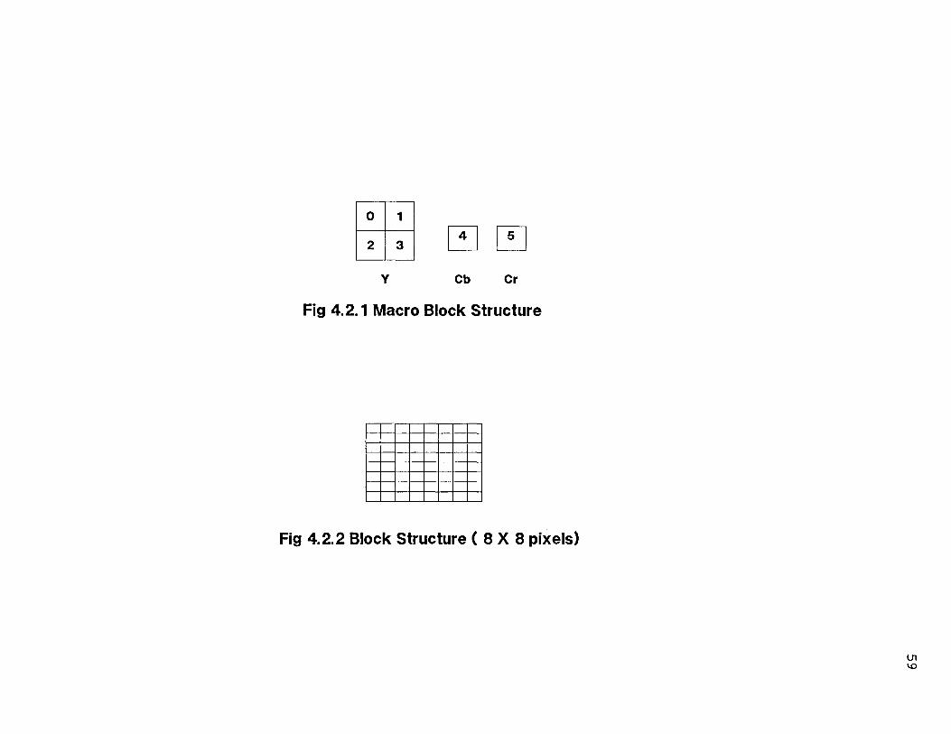
Fig 4.2.1 Macro Block Structure
Fig 4.2.2 Block Structure ( 8 X 8 pixels)
59
60
The coding scheme is arranged in layers corresponding to a hierarchical structure.
A picture corresponds to a single frame of motion video, or to a movie frame. Pictures
are collected into groups-of-pictures (GOP) for random access purposes, and a set of
groups of pictures forms a sequence which is the top coding layer. Pictures are divided
into slices to give some immunity to data corruption. Slices are divided into macro blocks
which are the units used for motion compensation and for changing the quantizer scale.
Macroblocks consist of an array of 16 X 16 pels ( a pel is sometimes called a pixel). Pels
are further divided into luma and chroma components. Each luma pel corresponds to one
picture pel, but since chroma information is subsampled with the 2:1 ratio both
horizontally and vertically, each chroma pel corresponds to 4 picture pels.
For convenience of coding, macro blocks are divided into six blocks of
component pels : four blocks of luma, one block of Cb chroma, and one block of Cr
chroma. This is shown in Fig 4.2.1.
Blocks are the basic coding units, and the DCT is applied at this block level. Each
block contains 64 component pels arranged in an 8 X 8 array as shown in Fig 4.2.2.
There are four picture types : I pictures, or intra pictures, which are coded without
any reference to any other pictures; P pictures, or predicted pictures, which are coded
using motion compensation from some previous and a future I or P picture, and B
pictures, or DC pictures, in which only the low frequency component (DC block average)
is coded and which are intended only for a fast forward search mode.
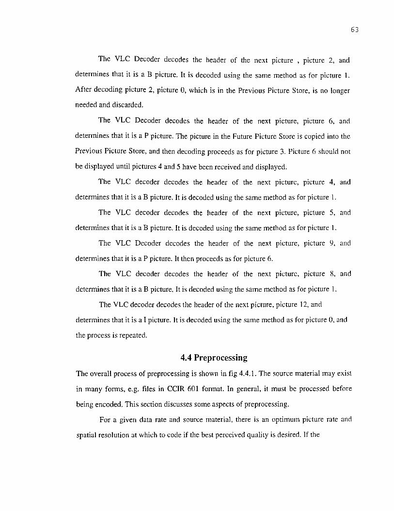
A typical coding scheme contains a mix of I,P, and B pictures. A typical scheme
may have an I picture about every 12 to 15 pictures, to give a reasonably fast random
access, and two B pictures inserted between each pair of I or P pictures. A typical
sequence of pictures, in display order, might be as shown in Fig 4.2.3.
The bitstream order, ie the order in which the pictures are transmitted , stored and
retrieved, is not the display order, but rather the order which the decoder requires them to
decode the bitstream. The bitstream order is shown in Fig 4.2.4.
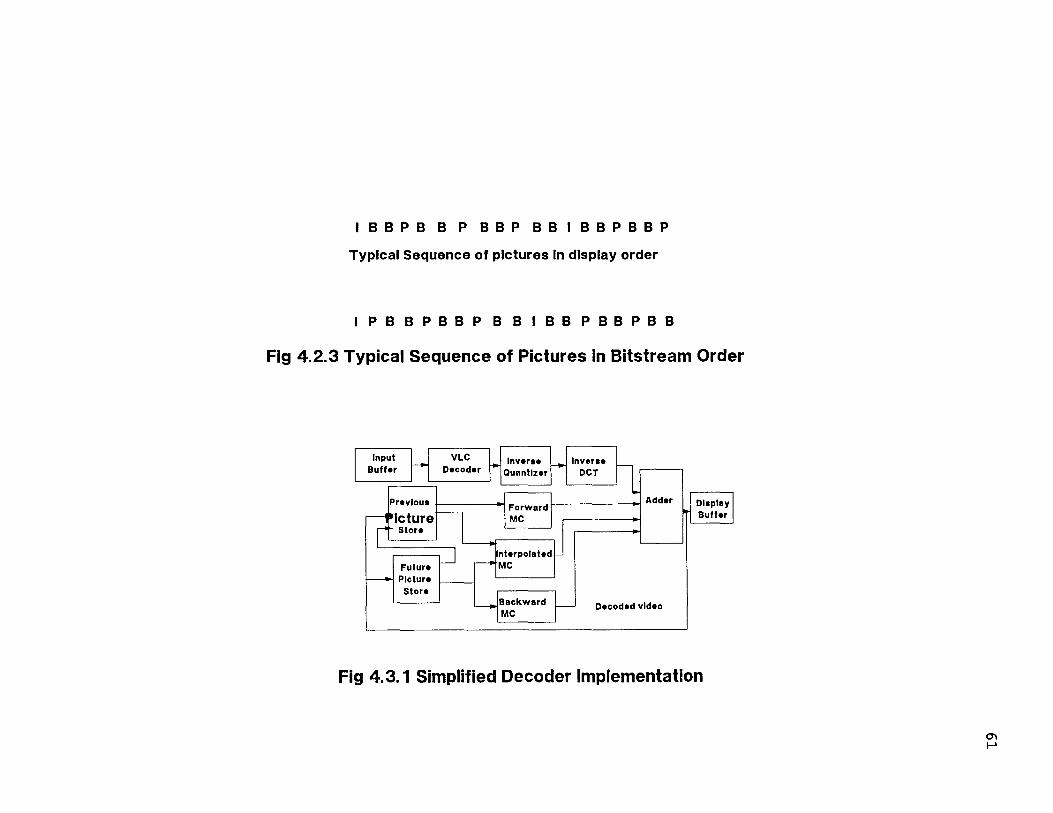
Fig 4.2.3 Typical Sequence of Pictures in Bitstream Order
Fig 4.3.1 Simplified Decoder Implementation
61
62
4.3 Simplified Decoder Model
A simplified block diagram of a possible decoder implementation is shown in Fig 4.3.1.
The input bitstream is accumulated in the Input Buffer until needed. The Variable
Length Code (VLC) Decoder decodes the header of the first picture, picture 0, and
determines that it is an I picture. The VLC Decoder produces indexes corresponding to
the quantized DCT coefficients using the appropriate quantization step size, which is
transmitted periodically . The coefficients are then transformed into pel values by the
Inverse DCT transformer and stored in the Previous Picture Store and the display buffer.
The picture may be displayed at the appropriate time.
The VLC Decoder decodes the head of the next picture, picture 3, and determines
that it is a P picture. For each block and the Inverse Quantizer produces the actual DCT
coefficients using the appropriate quantization step size.
The coefficients are then transformed into pel and added to the predicted block
produced by applying the motion vectors to the stored previous picture. The resultant
block is stored in the Future Picture Store and the Display Buffer. The picture cannot be
displayed until B pictures 1 and 2 have been received, decoded, and displayed.
The VLC Decoder decodes the header of the next picture, picture 1 , and
determines that it is a B picture. For each block, the VLC decoder produces motion
vectors giving the displacement from the stored previous or next pictures or both, and
indexes corresponding to the quantized DCT coefficients of the difference block. These
indices are then assembled for each block and the Inverse Quantizer produces the actual
DCT coefficients using the appropriate quantization step size. The coefficients are then
transformed into pel values and added to the predicted block produced by applying the
motion vectors to the stored pictures. The resultant block is then stored pictures. The
resultant block is then stored in the Display Buffer. It may be displayed at the appropriate
time.
63
The VLC Decoder decodes the header of the next picture , picture 2, and
determines that it is a B picture. It is decoded using the same method as for picture 1.
After decoding picture 2, picture 0, which is in the Previous Picture Store, is no longer
needed and discarded.
The VLC Decoder decodes the header of the next picture, picture 6, and
determines that it is a P picture. The picture in the Future Picture Store is copied into the
Previous Picture Store, and then decoding proceeds as for picture 3. Picture 6 should not
be displayed until pictures 4 and 5 have been received and displayed.
The VLC decoder decodes the header of the next picture, picture 4, and
determines that it is a B picture. It is decoded using the same method as for picture 1.
The VLC decoder decodes the header of the next picture, picture 5, and
determines that it is a B picture. It is decoded using the same method as for picture 1.
The VLC Decoder decodes the header of the next picture, picture 9, and
determines that it is a P picture. It then proceeds as for picture 6.
The VLC decoder decodes the header of the next picture, picture 8, and
determines that it is a B picture. It is decoded using the same method as for picture 1.
The VLC decoder decodes the header of the next picture, picture 12, and
determines that it is a I picture. It is decoded using the same method as for picture 0, and
the process is repeated.
4.4 Preprocessing
The overall process of preprocessing is shown in fig 4.4.1. The source material may exist
in many forms, e.g. files in CCIR 601 format. In general, it must be processed before
being encoded. This section discusses some aspects of preprocessing.
For a given data rate and source material, there is an optimum picture rate and
spatial resolution at which to code if the best perceived quality is desired. If the
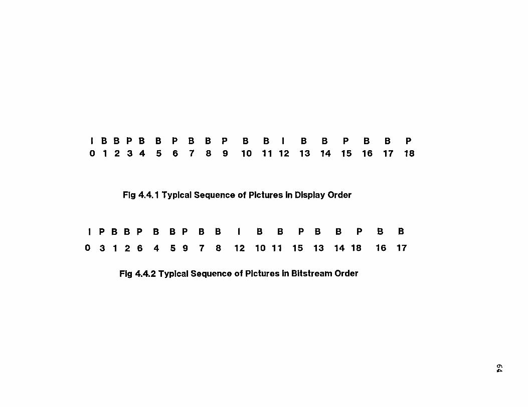
Fig 4.4.1 Typical Sequence of Pictures in Display Order
Fig 4.4.2 Typical Sequence of Pictures in Bitstream Order
64
65
resolution is too high, then too many bits will be expended on the overhead associated
with each block leaving too few to code the values of each pel accurately. If the
resolution is too high, then too many bits will be expanded on the overhead associated
with each block leaving too few to code the values of each pel accurately. If the
resolution is too high, then too many bits will be expanded on the overhead associated
with each block leaving too few to code the values of each pel accurately. If the
resolution is too low, the pel values will be rendered accurately, but high frequency
coding artifacts (e.g. noise and blockiness) and the perceived resolution and sharpness of
the image. This tradeoff is further complicated by the unknowns of the final viewing
conditions, eg screen brightness and the distance of the viewer from the screen.
At the data rates of 1 to 1.5 Mbps, a reasonable choice for the picture rate is 20 to
30 pps, for the horizontal resolution is between 250 and 400 pels, and for the vertical
resolution is between 200 and 300 pels.
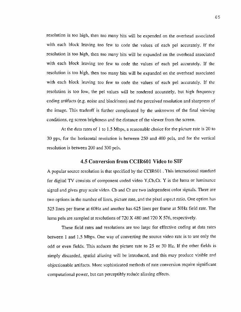
4.5 Conversion from CCIR601 Video to SIF
A popular source resolution is that specified by the CCIR601 . This international standard
for digital TV consists of component coded video Y,Cb,Cr. Y is the luma or luminance
signal and gives gray scale video. Cb and Cr are two independent color signals. There are
two options in the number of lines, picture rate, and the pixel aspect ratio. One option has
525 lines per frame at 60Hz and another has 625 lines per frame at 50Hz field rate. The
luma pels are sampled at resolutions of 720 X 480 and 720 X 576, respectively.
These field rates and resolutions are too large for effective coding at data rates
between 1 and 1.5 Mbps. One way of converting the source video rate is to use only the
odd or even fields. This reduces the picture rate to 25 or 30 Hz. If the other fields is
simply discarded, spatial aliasing will be introduced, and this may produce visible and
objectionable artifacts. More sophisticated methods of rate conversion require significant
computational power, but can perceptibly reduce aliasing effects.
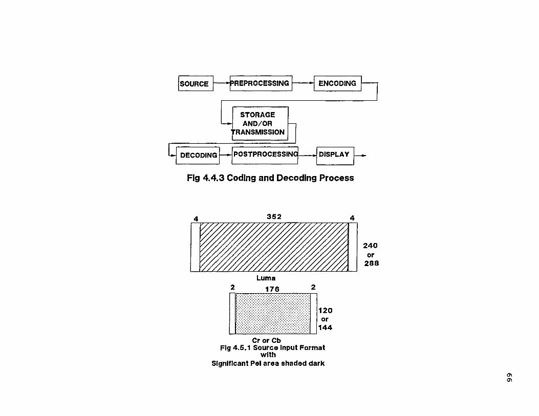
Fig 4.4.3 Coding and Decoding Process
Fig 4.5.1 Source Input Format with
Significant Pei area shaded dark
66
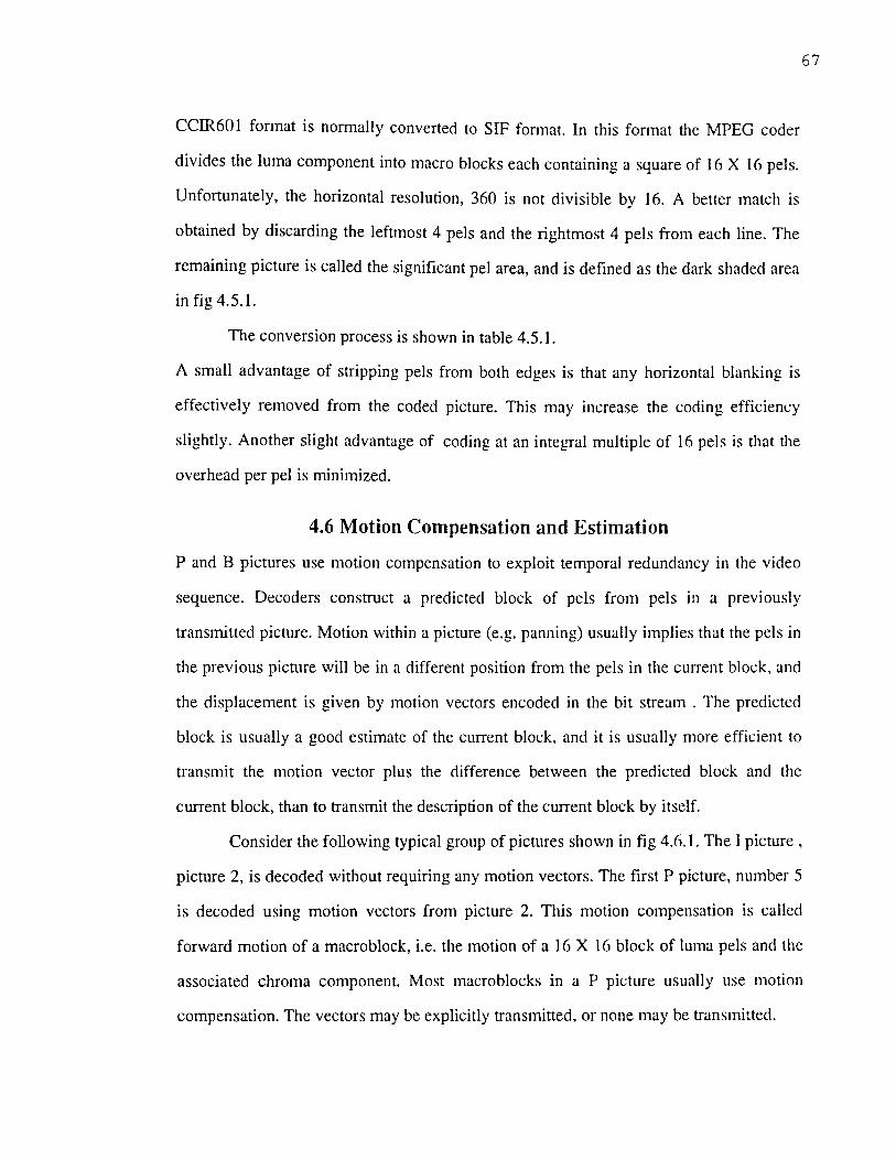
67
CCIR60 format is normally converted to SIF format. In this format the MPEG coder
divides the luma component into macro blocks each containing a square of 16 X 16 pels.
Unfortunately, the horizontal resolution, 360 is not divisible by 16. A better match is
obtained by discarding the leftmost 4 pels and the rightmost 4 pels from each line. The
remaining picture is called the significant pel area, and is defined as the dark shaded area
in fig 4.5.1.
The conversion process is shown in table 4.5.1.
A small advantage of stripping pels from both edges is that any horizontal blanking is
effectively removed from the coded picture. This may increase the coding efficiency
slightly. Another slight advantage of coding at an integral multiple of 16 pels is that the
overhead per pel is minimized.
4.6 Motion Compensation and Estimation
P and B pictures use motion compensation to exploit temporal redundancy in the video
sequence. Decoders construct a predicted block of pels from pels in a previously
transmitted picture. Motion within a picture (e.g. panning) usually implies that the pels in
the previous picture will be in a different position from the pels in the current block, and
the displacement is given by motion vectors encoded in the bit stream . The predicted
block is usually a good estimate of the current block, and it is usually more efficient to
transmit the motion vector plus the difference between the predicted block and the
current block, than to transmit the description of the current block by itself.
Consider the following typical group of pictures shown in fig 4.6.1. The I picture ,
picture 2, is decoded without requiring any motion vectors. The first P picture, number 5
is decoded using motion vectors from picture 2. This motion compensation is called
forward motion of a macroblock, i.e. the motion of a 16 X 16 block of luma pels and the
associated chroma component. Most macroblocks in a P picture usually use motion
compensation. The vectors may be explicitly transmitted, or none may be transmitted.
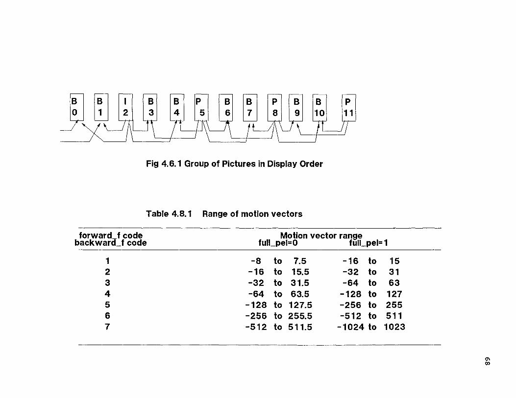
Fig 4.6.1 Group of Pictures in Display Order
Table 4.8.1 Range of motion vectors
68
69
The transmitted vectors usually have a precision of half a pel. The maximum
range of the vector is set by the forward_f parameter in the picture header. Sometimes, if
the motion is unusually large, the range may be doubled and the accuracy reduced to
integer pels, by the full_pel_forward_vector bit in the picture header.
A positive value of the horizontal or vertical component of the motion vector
signifies that the prediction is formed from the pixels in the referenced picture which are
spatially to the right or below the pixels predicted.
Not all the macroblocks in P picture use motion compensation. Some macro
blocks , as defined by the transmitted macroblock type, may be intra, and these are
reconstructed without motion compensation.
P picture number 8 uses forward motion compensation from picture 5. P picture
always use forward motion compensation from the last transmitted I or P picture.
The B pictures may use motion compensation from the previous I or P picture, or
from the next (in display order) I or P picture. This is equivalent to saying that they may
use motion compensation from the last two transmitted I or P pictures.
Prediction is called forward if reference is made to a picture in the past, and called
backward if reference is made to a picture in the future. For example, B picture 3 in fig
4.6.2 uses forward motion compensation from I picture 2, and backward motion
compensation from P picture 5. B pictures may use both forward and backward motion
compensation and average the result. This usage is called the interpolative motion
compensation.
All three types of motion compensation are useful, and are typically used in
coding B pictures. Interpolation prediction has the advantage of averaging any noise
present, and is frequently used if matching information is present in both previous and
future pictures. Forward or backward motion compensation may be more useful near the
edges of pictures, since the motion vectors cannot reference any pels that are outside the
edge of the picture, or where a foreground object is passing in front of a fixed or slow
70
moving background. The technique of coding with P or B pictures increases the coding
efficiency. B pictures can have greater errors of reconstruction than I or P pictures to
conserve coding bits, but since they are not used as the basis of motion compensation for
future pictures, these errors do not accumulate.
4.7 Motion Estimation
Motion compensation in a decoder is straight forward, but motion estimation in encoder,
presents a formidable computational challenge.
Various methods are available in the encoder. The more computationally
intensive methods tend to give better results, so there is a tradeoff to be made in the
encoder :computational power , and hence the cost, vs the video quality.
Using some search strategy the encoder attempts to match the pels in a
macroblock with those in a previous or future picture. The vector corresponding to the
best match is reported after the search is completed.
4.7.1 Block Matching Criterion
For matching, only the luma component is taken into consideration. Sufficient prediction
is obtained by matching only the luma component. The chroma vectors are only half the
amplitude of the luma vectors since the chroma bitmap resolution is one half that of the
luma.
In seeking a match , the encoder must decide whether to use the decoded past and
future pictures as the reference, or use the original past and future pictures. Note that the
decoder has no choice, it must use the decoded pictures since it does not have access to
the originals. Use of the decoded pictures by the encoder gives the smallest error in the
motion-compensated picture, whereas use of the original pictures gives the smallest error
in the motion vectors. The choice depends on whether the artifacts of increased noise,
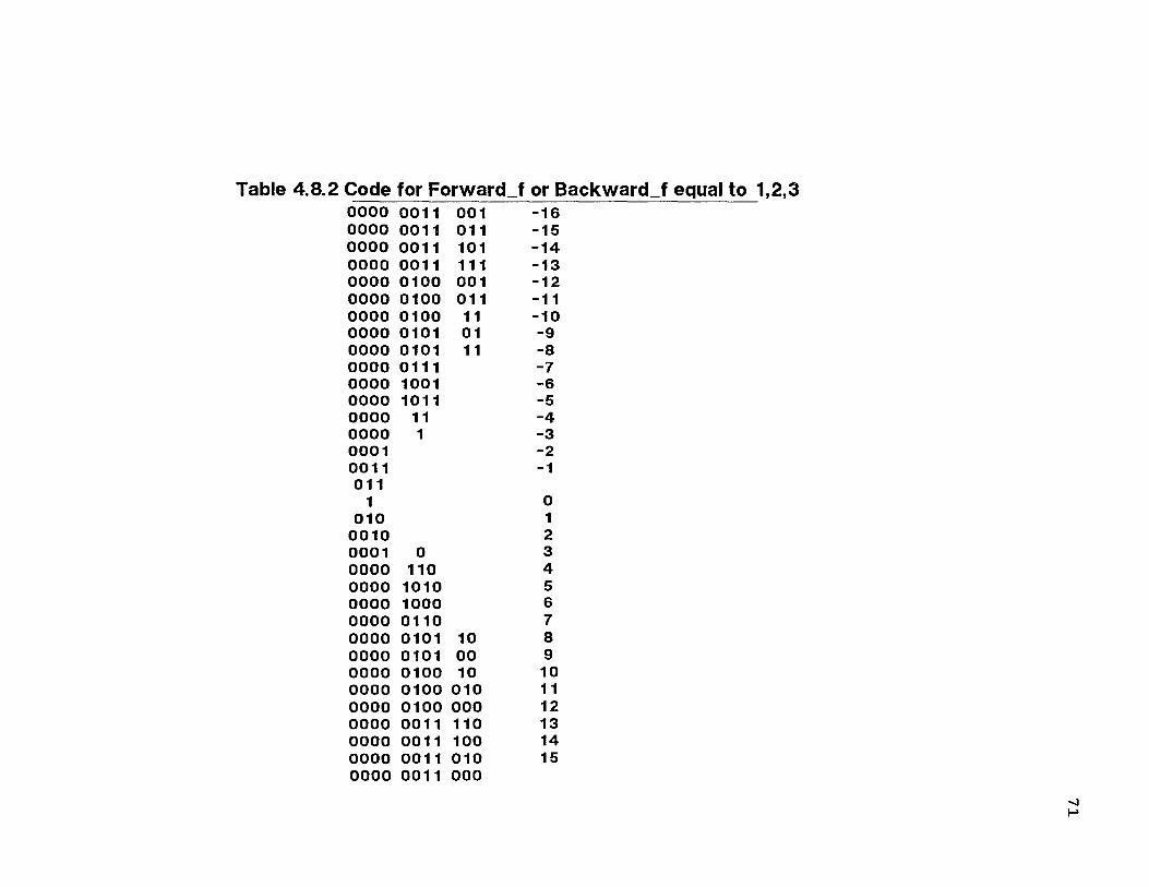
Table 4.8.2 Code for Forward_f or Backward_f equal to 1,2,3
71
72
or greater spurious motion are judged to be more objectional. There is usually little or no
difference in quality between the two methods, however the MPEG committee chose to
use the original pictures for the simulation results.
The mean square error of the difference between the motion compensated block
and the current block is one of the matching criterion. The other one being the mean
absolute difference between the motion-compensated block and the current block. This
method has been used for the simulation model since it is easier to compute using
software simulations.
4.8 Coding Of Motion Vectors
The motion vector of a macro block tends to be well correlated with the previous
macroblock. For example, in a pan all the vectors would be roughly the same. Motion
vectors are coded using a DPCM technique to make use of this correlation.
In P pictures the motion vectors used for DPCM, the prediction vector, is set to
zero at the start of each slice and at each intra coded macro block. Note that macro
blocks which are coded as predictive but which have no motion vector , also set the
prediction vector to zero i.e. when there is no motion associated.
In B pictures there are two prediction vectors, forward and backward. Each vector
is coded relative to the predicted vector of the same type . Both the prediction vectors are
set to zero at the start of each slice and at each intra-coded macro block. Note that
predictive macro blocks which have only forward vector do not affect the value of the
predicted backward vector. Similarly, predictive macro blocks which have only a
backward vector do not affect the value of the predicted forward vector.
The range of the vectors is set by two parameters- the full pel forward vector and
full pel backward vector flags in the picture header. These two parameters determine
whether the vectors are defined in half pel or integer pel units.
73
A second parameter, forward_f or backward_f, defines the number of bits
appended to the VLC codes in Table 4.8.1.
Advantage is taken of the fact that the range of displacement vector values is
constrained. Each VLC word will represent a pair of difference values. Only one of the
pair will yield a macro block vector falling within the permitted range. The range of the
vector is limited to the values shown in Table 4.8.2. The values obtained by decoding the
differential values must be kept within this range by adding or subtracting a modulus
which depends on the f value given in Table 4.8.3.
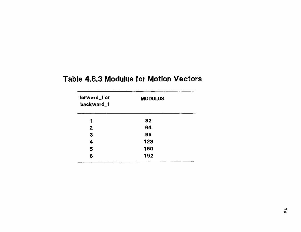
Table 4.8.3 Modulus for Motion Vectors
forward_f or
backward_f MODULUS
1 32
2 64
3 96
4 128
5 160
6 192
74
CHAPTER 5
RESULTS AND CONCLUSIONS
5.1 Hardware Implementation
The hardware designed for this project comprises of two boards- the interface to the
PC and the actual Compression board. The PC interface latches on the address and
the data from the address and the data bus of the PC. These are used by the
Compression board to generate the control signals.
Basically the PAL 22V10 gets activated by passing proper addresses to it.
This generates the control signals for the 74LS666 which generates the control
signals for the Compression chips and also latches on the initializing data.
I have been able to initialize and readback the initializing parameters to the 3
LSI Logic chips. The chips supplied to us was Engineering prototypes and not the
actual In-production chips. When I tried to pass the actual RGB data to the Raster to
Block Converter, it was not accepting anything as the BUSY signal, which should be
low while accepting data was always high. An order has been made to LSI Logic for
supplying us with the In-Production chips and we are awaiting the shipment.
CCUBE PC based JPEG hardware was used for simulations and comparative
study of JPEG and MPEG algorithms. For the MPEG algorithm , the simulation
software supplied by Bellcore was used. CCUBE card is a PC add-on card and accept
TARGA sequences as inputs. The outputs are also in the TARGA format.
TARGA format is explained here :
1) TARGA Header (18 bits)
2) Blue value (5 bits)
3) Green value (5 bits)
4) Red value (5bits).
5) Padding (1 bit)
It is actually 16 bits/pixel with RGB getting each 5 bits with 1 bit being unused.
75
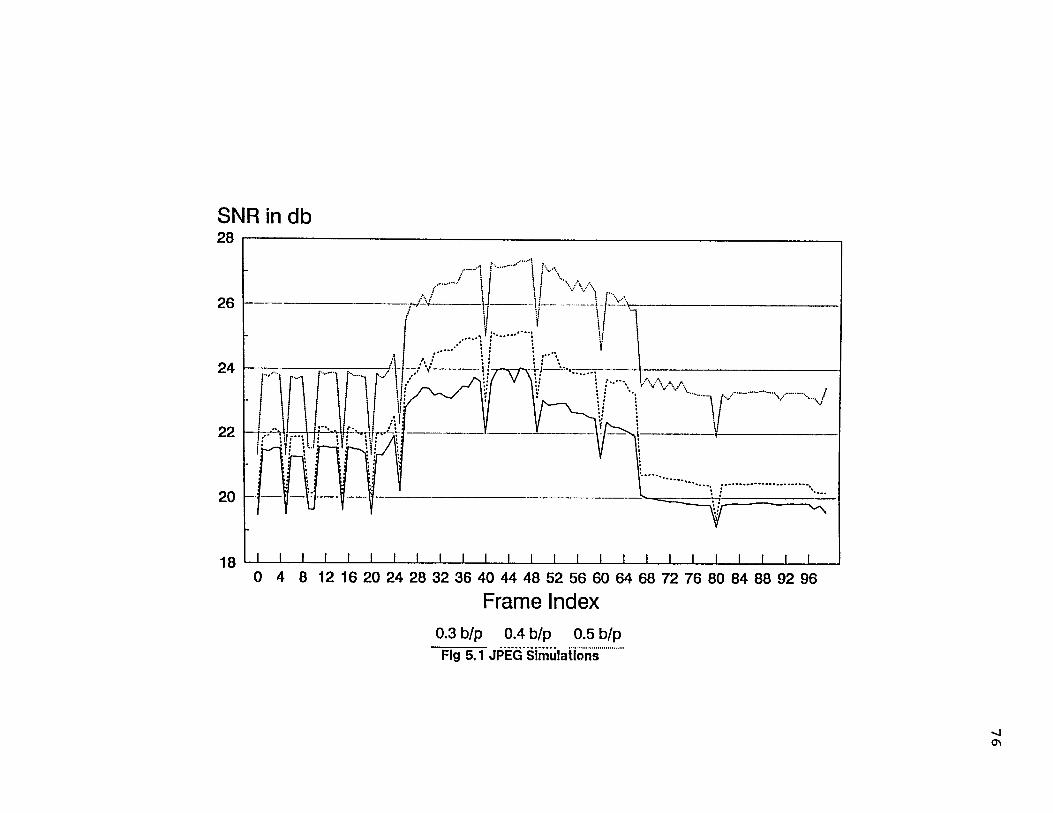
Fig 5.1 JPEG Simulations
76
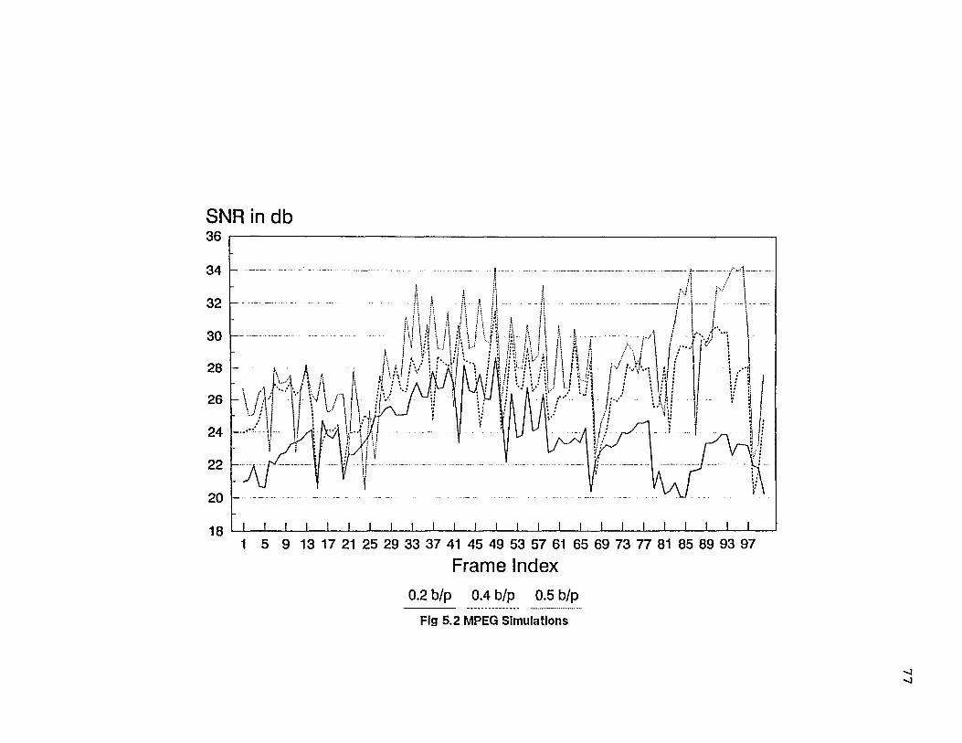
Fig 5.2 MPEG Simulations
77
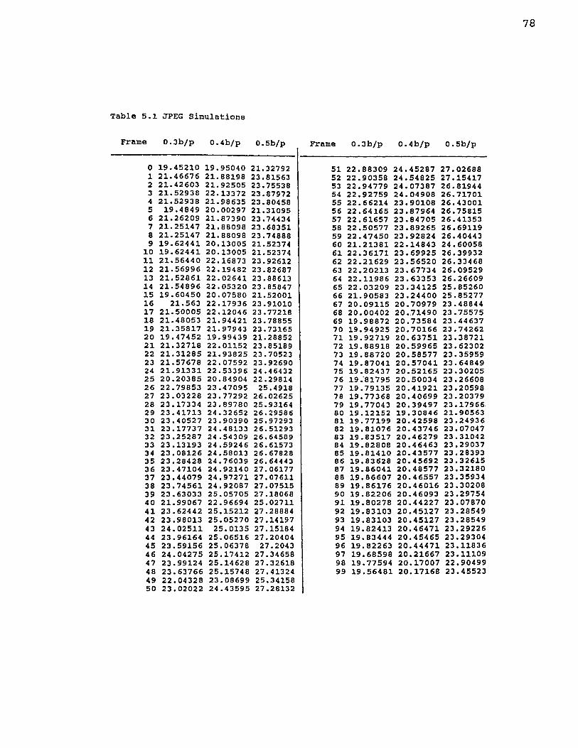
Table 5.1 JPEG Simulations
78
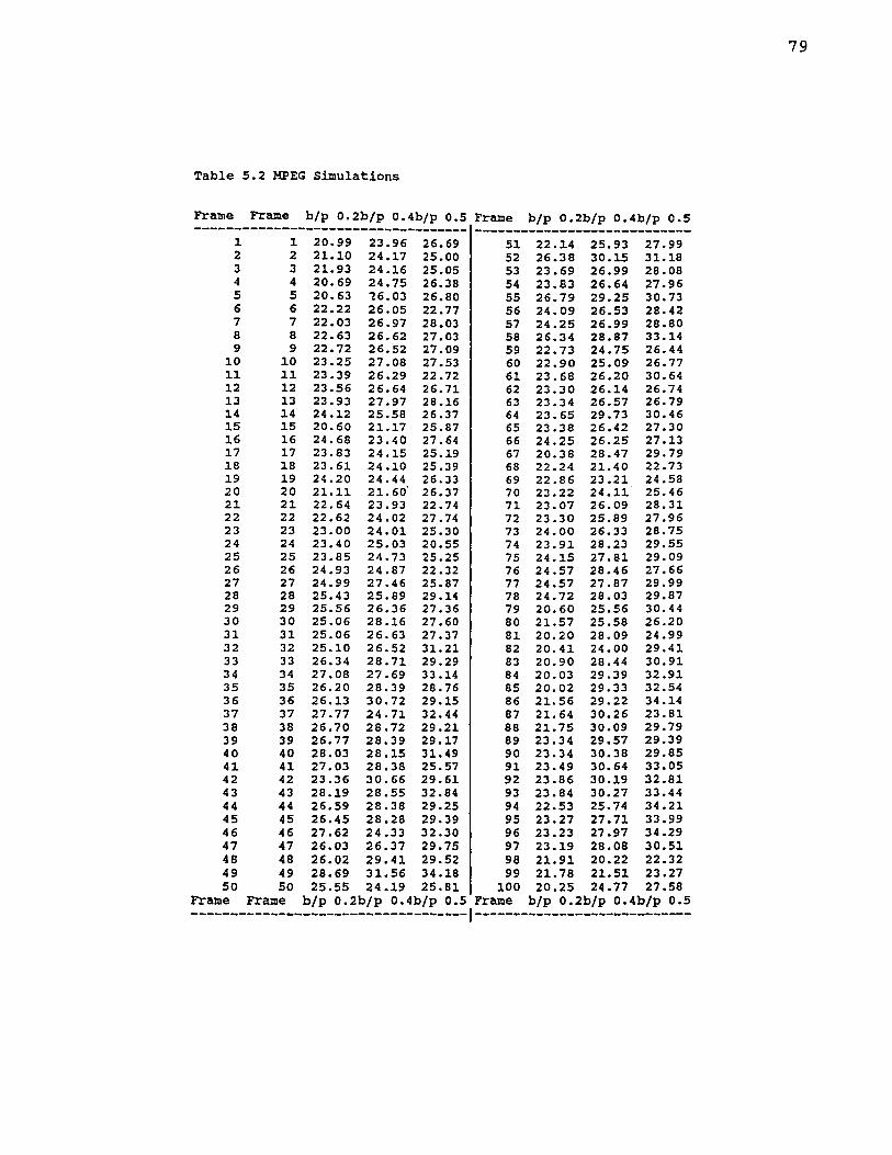
Table 5.2 MPEG Simulations
79
80
5.2 Simulations
Simulations were carried out with standard test sequence (table tennis) on the existing
CCUBE JPEG hardware and Optibase MPEG software. The resulting SNR for
various compression ratios were calculated. The output filesize was varied in the
JPEG hardware and hence the bits/pel was varied. The input files are in Targa format
which is explained in the next section. The output files are also created in Targa
format. The resulting SNR between the input and output Targa files were calculated
and tabulated. Table 5.1 gives the SNR for JPEG simulations for 0.2,0.3,0.4 bits/pel.
MPEG simulation software creates output SIF files. These were converted into Targa
files and the resulting SNR between the input and output Targa files were calculated.
Table 5.2 gives the results obtained for the MPEG simulation.
Fig 5.3 gives the plot for frame index vs SNR for JPEG and fig 5.4 gives the
plot for MPEG.
5.3 Conclusions and Future Directions
The results of the video codec simulation clearly indicate that for the same bit rate
and bits/pel MPEG gives a much higher SNR than JPEG. However for low bit rates
the performance of JPEG is commendable and much less complex than MPEG.
In the area of lossy compression the most obvious additional capability to add
to JPEG is adaptive quantization. For a given image quality it has been noted that
compression could be improved by as much as 30% by adaptive quantization.
Adaptive quantization is however not a cost free option, because the
determination of the quantization values that are used with a given DCT block can be
a computational burden, and provision for multiple quantization tables or scaling of
quantization table values in the encoder and decoder must be provided. The methods
adopted to select the actual quantization table to be used for a particular set of image
could be time consuming and the hardware could become more complex. Although
the JPEG committee's decision not to include adaptive quantization can be defended
81
on the basis of simplicity, there is no question that adaptive quantization would
significantly improve image quality at a given bit rate.
The most obvious way of introducing adaptive quantization would be to
encode a binary decision at the beginning of each MCU to tell the decoder when new
quantization tables ( or modification of tables) are needed. The arithmetic coder could
code this as a single binary decision, perhaps conditioned on the preceding adaptive
quantization decision. For best coding efficiency , the Huffman coder would probably
need to run-length encode the sequence of adaptive quantization decisions.
Alternatively, a "table switch " code could be defined for selecting from a predefined
tables.
MPEG encoder is highly complex. As of now MPEG decoders are floating in
the market with few encoders. Work is yet to be done to simplify MPEG encoder.
The most difficult part in an encoder is the motion estimation. The search methods
adopted by the encoder i.e, the logarithmic search and pixel recursive search are time
consuming when it comes to hardware implementation. Work has to be done in this
area for simplifying the hardware for this purpose.

APPENDIX
The appendix contains a listing of the software used for initializing and controlling the
LSI Logic chips and the conversion between YCbCr and RGB color space coordinates.
82
83
/ * This program initializes the L64765 */
#include<stdio.h> #include<conio.h> #include<stdlib.h> #include<dos.h> #include "init.h" #define BASE 0x2a0 #define ctrlw 0x2002 #define dataw 0x2004 #define datarb 0x2005 #define ctrlrb 0x2003 #define initw 0x2008 #define rw 0x0000 #define cw 0x0006 #define gw 0x0002 #define bw 0x0004
#define HSYNC 0x08 #define VSYNC 0x02 #define CLK 0x04
unsigned dat[]={0x30,0x00,0x30,0x00,0x00,0x00,0x00,0x00}; /* Window parameters */
unsigned data[48];
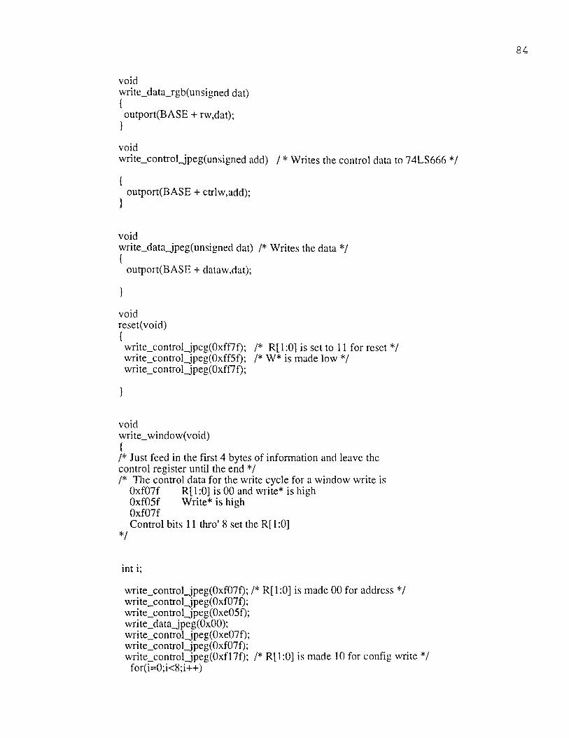
int i;
write_control_jpeg(0xf07f); /* R[1:0] is made 00 for address */ write_control_jpeg(0xf07f); write_control_jpeg(0xe05f); write_data_jpeg(0x00); write_control_jpeg(0xe070; write_control_jpeg(0xf07f); write_control_jpeg(0xf17f); /* R[1:0] is made 10 for config write */
for(i=0;i<8;i++)
84
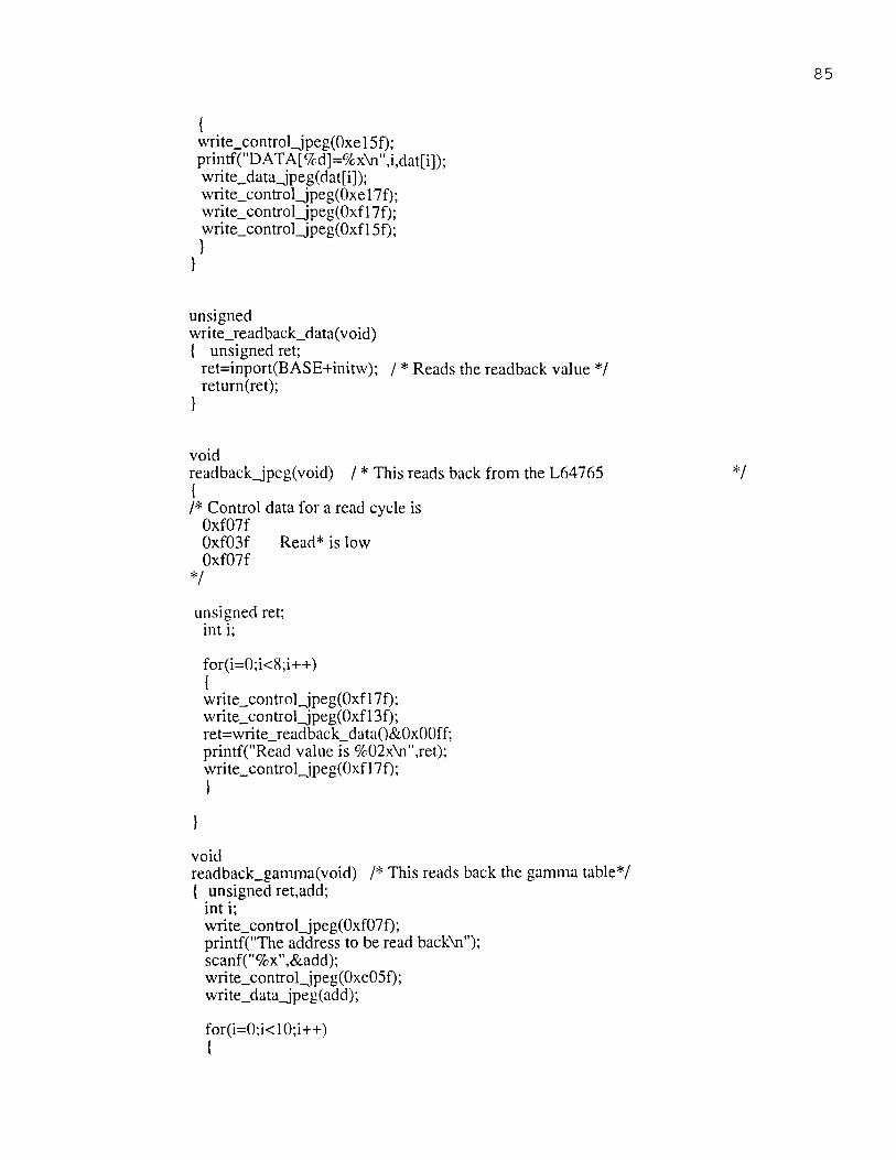
85

86
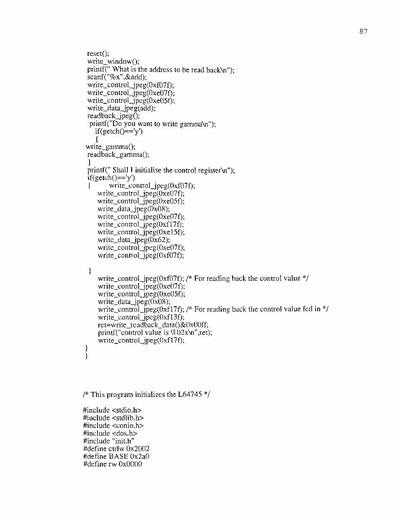
/* This program initializes the L64745 */
#include <stdio.h> #include <stdlib.h> #include <conio.h> #include <dos.h> #include "init.h" #define ctrlw 0x2002 #define BASE 0x2a0 #define rw 0x0000
87
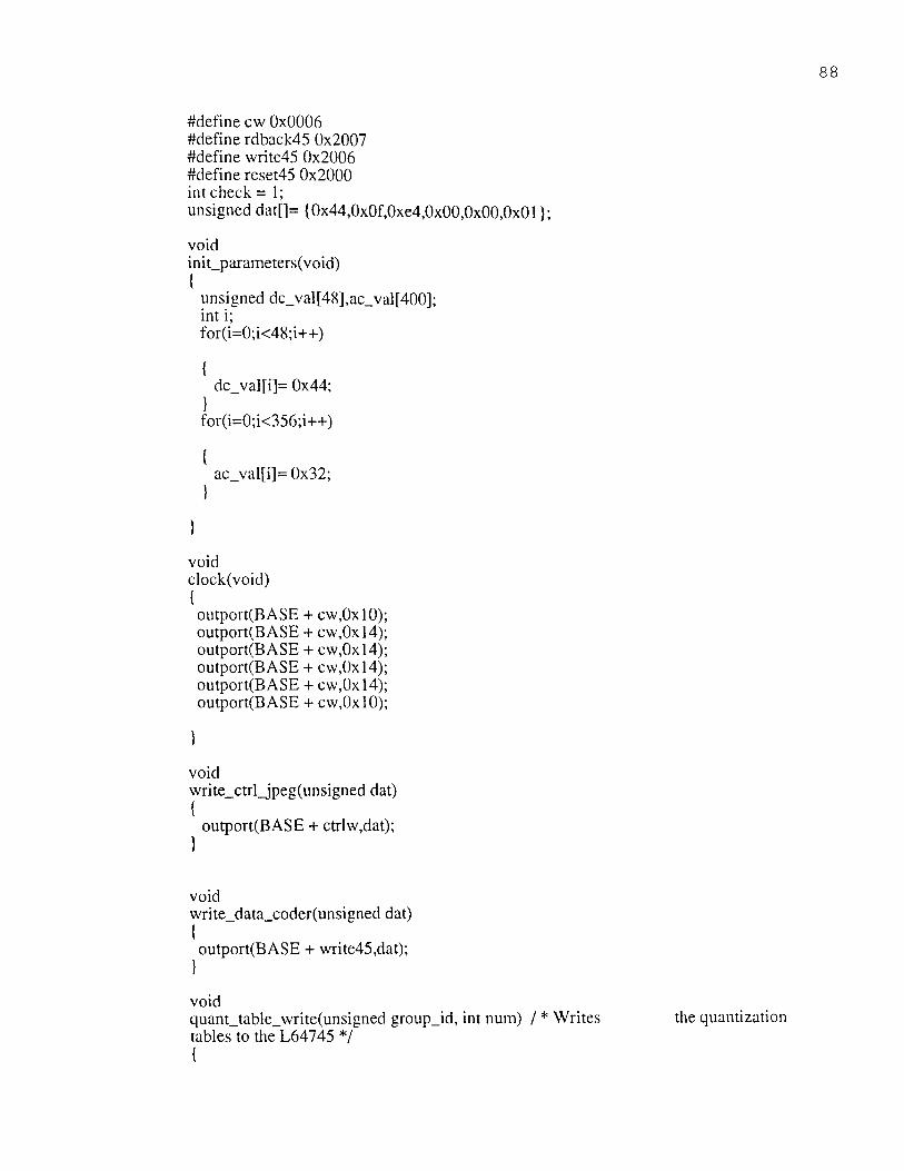
#define cw 0x0006 #define rdback45 0x2007 #define write45 0x2006 #define reset45 0x2000 int check = 1; unsigned dat[]= (0x44,0x0f,0xe4,0x00,0x00,0x01);
88
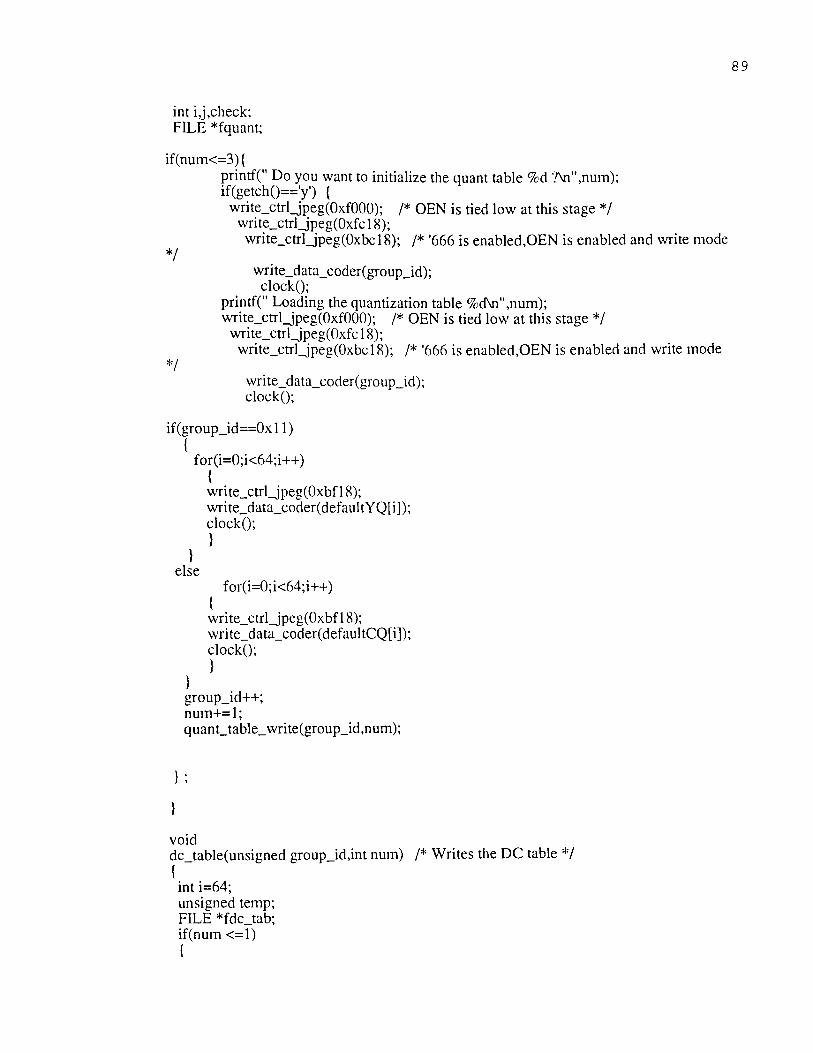
89
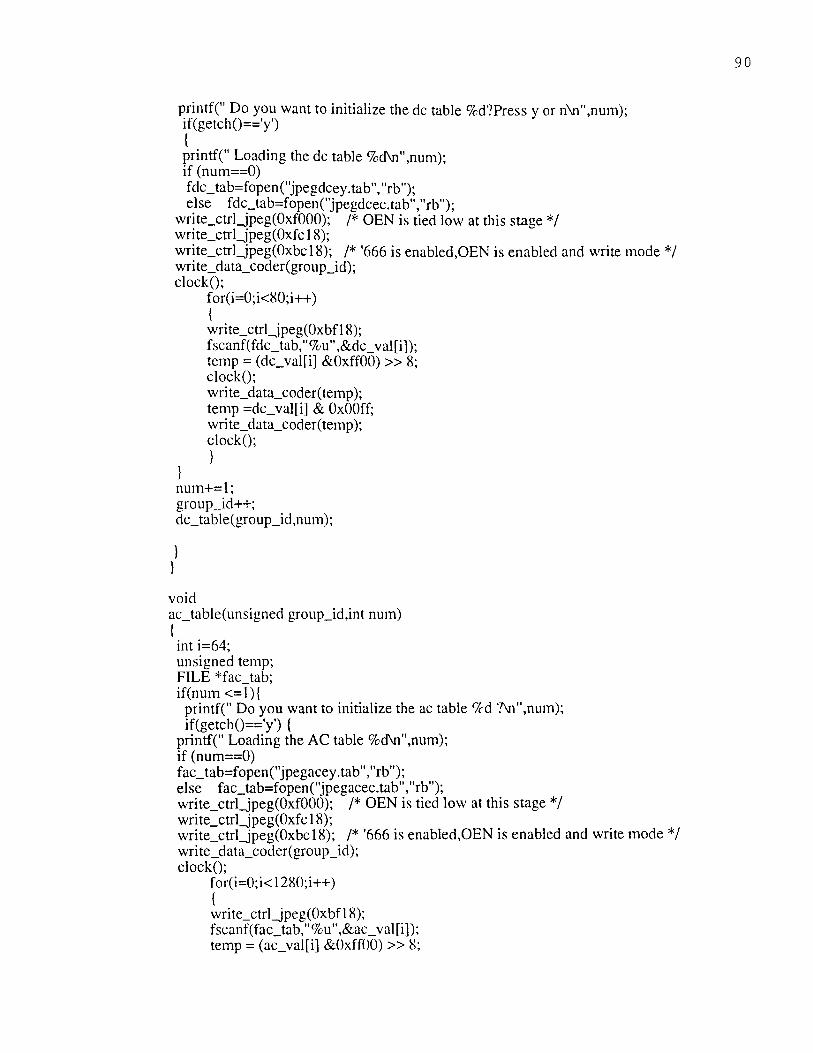
90
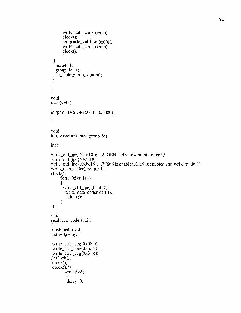
91
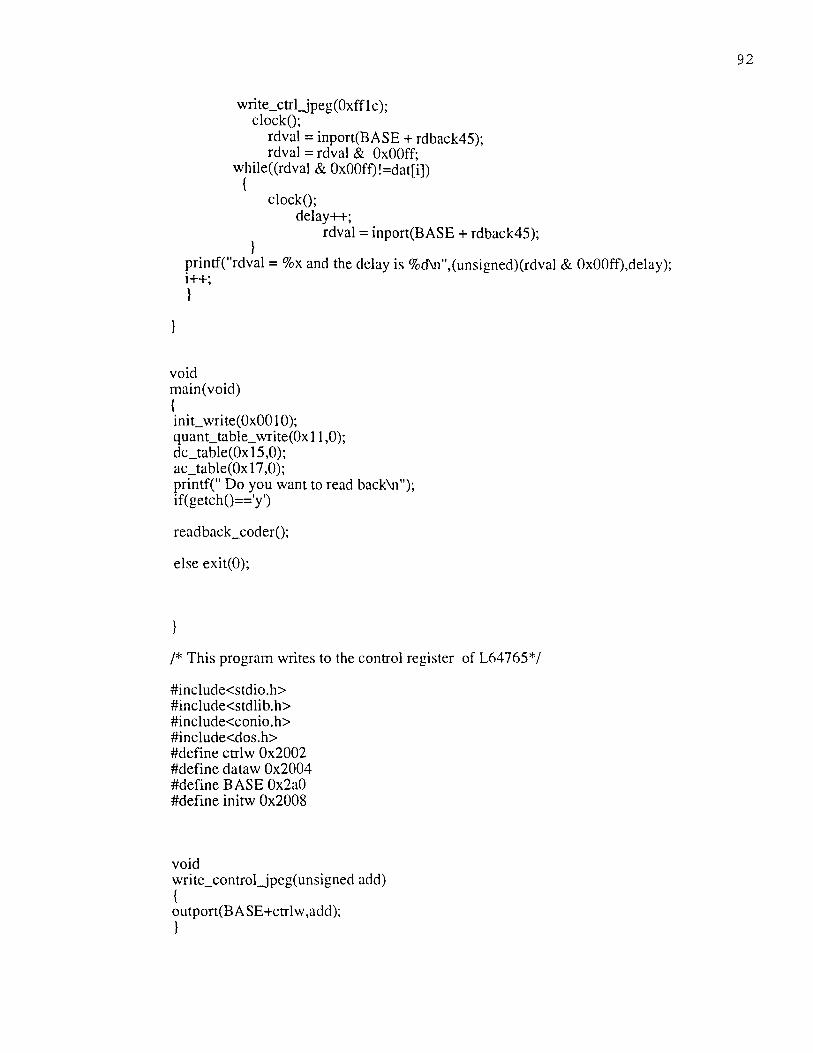
92
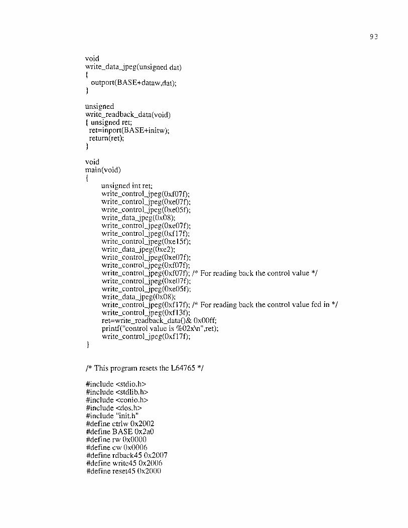
/* This program resets the L64765 */
#include <stdio.h> #include <stdlib.h> #include <conio.h> #include <dos.h> #include "init.h" #define ctrlw 0x2002 #define BASE 0x2a0 #define rw 0x0000 #define cw 0x0006 #define rdback45 0x2007 #define write45 0x2006 #define reset45 0x2000
93
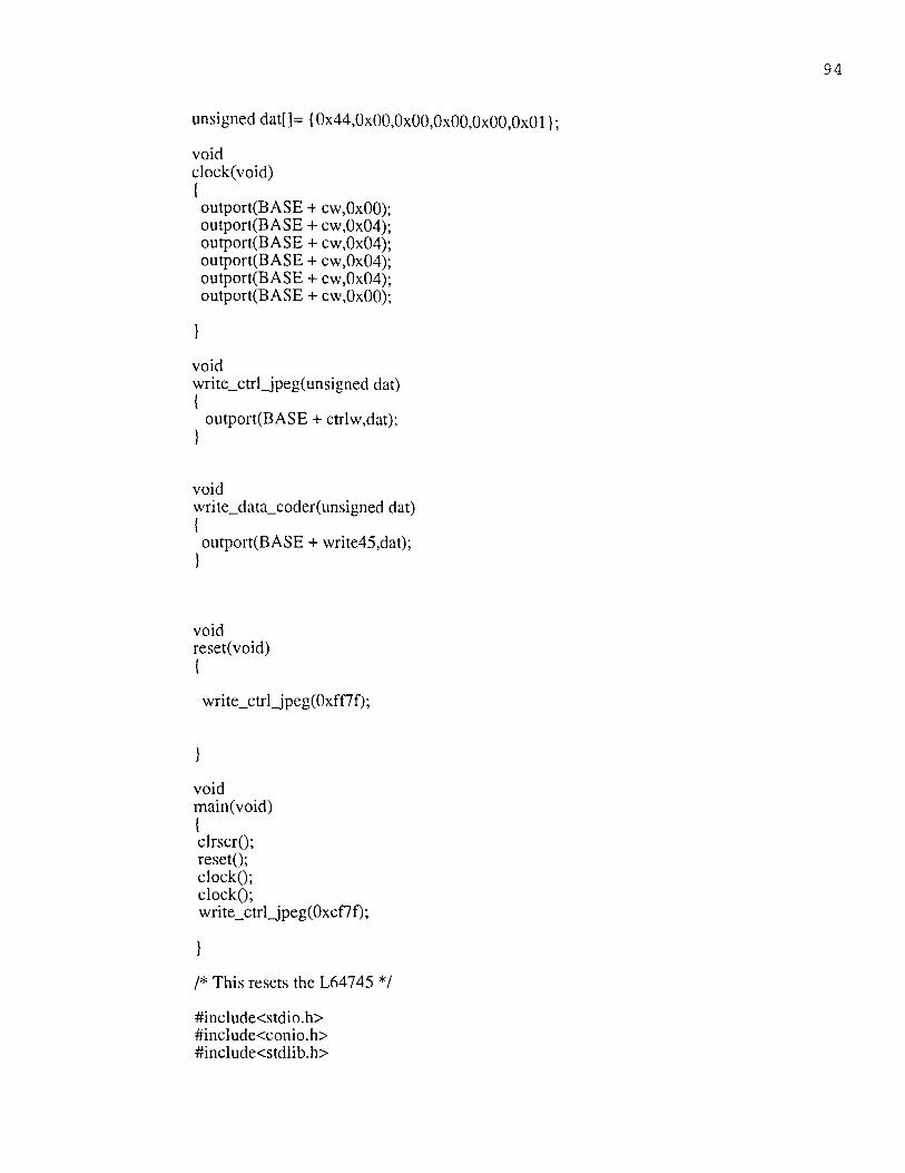
/* This resets the L64745 *I
#include<stdio.h> #include<conio.h> #include<stdlib.h>
94
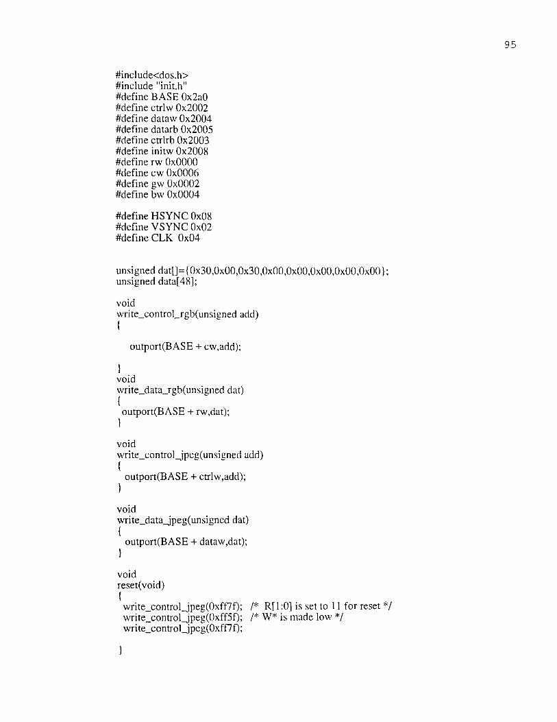
#include<dos.h> #include "init.h" #define BASE 0x2a0 #define ctrlw 0x2002 #define dataw 0x2004 #define datarb 0x2005 #define ctrlrb 0x2003 #define initw 0x2008 #define rw 0x0000 #define cw 0x0006 #define gw 0x0002 #define bw 0x0004
#define HSYNC 0x08 #define VSYNC 0x02 #define CLK 0x04
unsigned dat[]={0x30,0x00,0x30,0x00,0x00,0x00,0x00,0x00}; unsigned data[48];
95

96
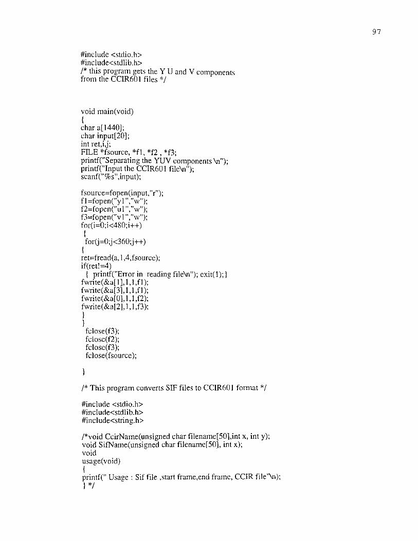
#include <stdio.h> #include<stdlib.h> /* this program gets the Y U and V components from the CCIR601 files */
/* This program converts SIF files to CCIR601 format */
#include <stdio.h> #include<stdlib.h> #include<string.h>
97
98
99
100
#include <stdio.h> #include <stdlib.h>
#include "tgarhb.h" TGAHeader th ={0,0,2,0,0,0,0,0,512,480,16,32};
101
102
103
104
105
106
112
REFERENCES
1. Dr Rashid Ansari, Fure Ching Jeng, Andria Wong. MPEG Simulation Manual,1990.
2. William Pennebaker, Joan L. Michell. JPEG Still Image Data Compression Standard , Van Nostrand Reinhold, NY, 1993.
3. LSI LOGIC: LSI Chipset manual for JPEG algorithm,1990.
4. F.Rocca and S. Zanoleth. Bandwidth reduction via movement compensation on a model of a random video process, IEEE trans. Comm, vol COM-20, pp 960-
-965, Oct 1972.
5. JPEG Committee. JPEG Draft .1989.
6. A.K. Jain. Fundamentals of Digital Image Processing, Englewood Cliffs, NJ: Prentice Hall,1989.
7. N.Ahmed, T.Natarajan, and K.R Rao. Discrete Cosine Transform. IEEE Transactions, Computers, C-2390-3 (Jan 1974).
8. P.Elias and N.Abramson. Information theory and Coding. New York: McGraw Hill Book Co, 1963.
9. M.Rabbani and P.W Jones. Digital Image Compression Techniques. Vol TT7. pp 1-221, Bellingham, WA:SPIE.
10. R.B Arps, T.K Truong, D.J Lu, R.0 Pasco, and T.D Friedman. A multi purpose VLSI chip for adaptive data compression techniques. IBM J.Res. Develop. 32(6):775-95 (Nov.1988).
11. J.G Cleary, I.H Witten, and R.M. Neal. Arithmetic Coding for Data Compression. Communic of the ACM. 30(6):520-40 (Jun 1987).
12. A.LigtenBerg, R.H Wright, and J.H.O'Neill. A VLSI Ortogonal Transform for Real time Image Compression. Visual Communication & Image Process. (Oct 1987).
13. B.D. Tseng and W.C Miller. On Computing the Discrete Cosine Transforms. IEEE Trans. on Computers. C27(10):1966-8.
14. D.A Huffman. A method for the construction of Minimum- Redundancy Codes. Proc. IRE. 40(9):1098-101 (Sept 1952).
15. D.S Thornton and K.L Anderson. A BNF for the JPEG Image Compression Header Structure. Proceedings Electronic Imaging '90 East, pp96-99. Boston, MA (Oct 29- Nov 1,1990).
16. G.G Langdon and J.J Rissanen . Compression of Black and White Images with Arithmetic coding. IEEE trans. on Commun. 29(6):858-67 (Jun. 1981).
113
17. C.B Jones. An Efficient Coding System for Long Source Sequences. IEEE Trans Info Theory. IT-27(3):280-91 ( May 1991).
18. JJ Rissanen and G.G Langdon. Arithmetic Coding. IBM J. Res. Develop. 23(2):149-62 (Mar. 1979).
19. J.G Cleary, I.H Witten, and R.M. Neal. Arithmetic Coding for Data Compression. Commu. of the ACM. 30(6):520-40 (Jun.1987).
Related Documents