Yale University Yale University EliScholar – A Digital Platform for Scholarly Publishing at Yale EliScholar – A Digital Platform for Scholarly Publishing at Yale Yale Graduate School of Arts and Sciences Dissertations Spring 2021 Hardware Architectures for Post-Quantum Cryptography Hardware Architectures for Post-Quantum Cryptography Wen Wang Yale University Graduate School of Arts and Sciences, [email protected] Follow this and additional works at: https://elischolar.library.yale.edu/gsas_dissertations Recommended Citation Recommended Citation Wang, Wen, "Hardware Architectures for Post-Quantum Cryptography" (2021). Yale Graduate School of Arts and Sciences Dissertations. 242. https://elischolar.library.yale.edu/gsas_dissertations/242 This Dissertation is brought to you for free and open access by EliScholar – A Digital Platform for Scholarly Publishing at Yale. It has been accepted for inclusion in Yale Graduate School of Arts and Sciences Dissertations by an authorized administrator of EliScholar – A Digital Platform for Scholarly Publishing at Yale. For more information, please contact [email protected].

Welcome message from author
This document is posted to help you gain knowledge. Please leave a comment to let me know what you think about it! Share it to your friends and learn new things together.
Transcript

Yale University Yale University
EliScholar – A Digital Platform for Scholarly Publishing at Yale EliScholar – A Digital Platform for Scholarly Publishing at Yale
Yale Graduate School of Arts and Sciences Dissertations
Spring 2021
Hardware Architectures for Post-Quantum Cryptography Hardware Architectures for Post-Quantum Cryptography
Wen Wang Yale University Graduate School of Arts and Sciences, [email protected]
Follow this and additional works at: https://elischolar.library.yale.edu/gsas_dissertations
Recommended Citation Recommended Citation Wang, Wen, "Hardware Architectures for Post-Quantum Cryptography" (2021). Yale Graduate School of Arts and Sciences Dissertations. 242. https://elischolar.library.yale.edu/gsas_dissertations/242
This Dissertation is brought to you for free and open access by EliScholar – A Digital Platform for Scholarly Publishing at Yale. It has been accepted for inclusion in Yale Graduate School of Arts and Sciences Dissertations by an authorized administrator of EliScholar – A Digital Platform for Scholarly Publishing at Yale. For more information, please contact [email protected].

Abstract
Hardware Architectures for
Post-Quantum Cryptography
Wen Wang
2021
The rapid development of quantum computers poses severe threats to many commonly-
used cryptographic algorithms that are embedded in different hardware devices to ensure
the security and privacy of data and communication. Seeking for new solutions that are po-
tentially resistant against attacks from quantum computers, a new research field called Post-
Quantum Cryptography (PQC) has emerged, that is, cryptosystems deployed in classical
computers conjectured to be secure against attacks utilizing large-scale quantum comput-
ers. In order to secure data during storage or communication, and many other applications
in the future, this dissertation focuses on the design, implementation, and evaluation of
efficient PQC schemes in hardware.
Four PQC algorithms, each from a different family, are studied in this dissertation.
The first hardware architecture presented in this dissertation is focused on the code-based
scheme Classic McEliece. The research presented in this dissertation is the first that builds
the hardware architecture for the Classic McEliece cryptosystem. This research successfully
demonstrated that complex code-based PQC algorithms can be run efficiently on hardware.
Furthermore, this dissertation shows that implementation of this scheme on hardware can
be easily tuned to different configurations by implementing support for flexible choices of
security parameters as well as configurable hardware performance parameters. The suc-
cessful prototype of the Classic McEliece scheme on hardware increased confidence in this
scheme, and helped Classic McEliece to get recognized as one of seven finalists in the third
round of the NIST PQC standardization process.
While Classic McEliece serves as a ready-to-use candidate for many high-end applica-
tions, PQC solutions are also needed for low-end embedded devices. Embedded devices
play an important role in our daily life. Despite their typically constrained resources, these

devices require strong security measures to protect them against cyber attacks. Towards
securing this type of devices, the second research presented in this dissertation focuses
on the hash-based digital signature scheme XMSS. This research is the first that explores
and presents practical hardware based XMSS solution for low-end embedded devices. In
the design of XMSS hardware, a heterogeneous software-hardware co-design approach was
adopted, which combined the flexibility of the soft-core with the acceleration from the
hard-core. The practicability and efficiency of the XMSS software-hardware co-design is
further demonstrated by providing a hardware prototype on an open-source RISC-V based
System-on-a-Chip (SoC) platform.
The third research direction covered in this dissertation focuses on lattice-based cryp-
tography, which represents one of the most promising and popular alternatives to today’s
widely adopted public key solutions. Prior research has presented hardware designs tar-
geting the computing blocks that are necessary for the implementation of lattice-based
systems. However, a recurrent issue in most existing designs is that these hardware designs
are not fully scalable or parameterized, hence limited to specific cryptographic primitives
and security parameter sets. The research presented in this dissertation is the first that
develops hardware accelerators that are designed to be fully parameterized to support dif-
ferent lattice-based schemes and parameters. Further, these accelerators are utilized to
realize the first software-harware co-design of provably-secure instances of qTESLA, which
is a lattice-based digital signature scheme. This dissertation demonstrates that even de-
manding, provably-secure schemes such as qTESLA can be realized efficiently with proper
use of software-hardware co-design.
The final research presented in this dissertation is focused on the isogeny-based scheme
SIKE, which recently made it to the final round of the PQC standardization process. This
research shows that hardware accelerators can be designed to offload compute-intensive
elliptic curve and isogeny computations to hardware in a versatile fashion. These hardware
accelerators are designed to be fully parameterized to support different security parameter
sets of SIKE as well as flexible hardware configurations targeting different user applications.
This research is the first that presents versatile hardware accelerators for SIKE that can
be mapped efficiently to both FPGA and ASIC platforms. Based on these accelerators,

an efficient software-hardware co-design is constructed for speeding up SIKE. In the end,
this dissertation demonstrates that, despite being embedded with expensive arithmetic, the
isogeny-based SIKE scheme can be run efficiently by exploiting specialized hardware.
These four research directions combined demonstrate the practicability of building effi-
cient hardware architectures for complex PQC algorithms. The exploration of efficient PQC
solutions for different hardware platforms will eventually help migrate high-end servers and
low-end embedded devices towards the post-quantum era.

Hardware Architectures for
Post-Quantum Cryptography
A DissertationPresented to the Faculty of the Graduate School
ofYale University
in Candidacy for the Degree ofDoctor of Philosophy
byWen Wang
Dissertation Director: Jakub Szefer
June 2021

c© 2021 by Wen Wang
All rights reserved.

Contents
Acknowledgements xv
1 Introduction 1
1.1 Post-Quantum Cryptography on Hardware . . . . . . . . . . . . . . . . . . 1
1.2 Dissertation Contributions . . . . . . . . . . . . . . . . . . . . . . . . . . . . 2
1.3 Dissertation Outline . . . . . . . . . . . . . . . . . . . . . . . . . . . . . . . 3
2 Preliminaries 6
2.1 Modern Cryptography . . . . . . . . . . . . . . . . . . . . . . . . . . . . . . 6
2.1.1 Symmetric-Key Cryptography . . . . . . . . . . . . . . . . . . . . . . 7
2.1.2 Public-Key Cryptography . . . . . . . . . . . . . . . . . . . . . . . . 8
2.2 Quantum Threats on Modern Cryptography . . . . . . . . . . . . . . . . . . 12
2.3 Families of Post-Quantum Cryptograhy . . . . . . . . . . . . . . . . . . . . 13
2.3.1 Code-Based Cryptography . . . . . . . . . . . . . . . . . . . . . . . . 14
2.3.2 Hash-Based Cryptography . . . . . . . . . . . . . . . . . . . . . . . . 15
2.3.3 Lattice-Based Cryptography . . . . . . . . . . . . . . . . . . . . . . . 16
2.3.4 Isogeny-Based Cryptography . . . . . . . . . . . . . . . . . . . . . . 17
2.4 Cryptographic Implementations . . . . . . . . . . . . . . . . . . . . . . . . . 18
2.4.1 Cryptography in Hardware . . . . . . . . . . . . . . . . . . . . . . . 19
2.4.2 Design Methodologies for Cryptographic Hardware . . . . . . . . . . 20
2.5 Hardware Platforms for Prototyping . . . . . . . . . . . . . . . . . . . . . . 21
2.5.1 Field Programmable Gate Arrays . . . . . . . . . . . . . . . . . . . . 22
2.5.2 Application Specific Integrated Circuits . . . . . . . . . . . . . . . . 23
iii

2.5.3 FPGA Designs vs. ASIC Designs . . . . . . . . . . . . . . . . . . . . 24
3 Code-based Cryptography: Classic McEliece Cryptosystem on Hardware 25
3.1 Background . . . . . . . . . . . . . . . . . . . . . . . . . . . . . . . . . . . . 25
3.1.1 Related Work . . . . . . . . . . . . . . . . . . . . . . . . . . . . . . . 26
3.1.2 Motivation for Our Work . . . . . . . . . . . . . . . . . . . . . . . . 27
3.2 Classic McEliece and the Niederreiter Cryptosystem . . . . . . . . . . . . . 28
3.2.1 Key Generation . . . . . . . . . . . . . . . . . . . . . . . . . . . . . . 30
3.2.2 Encryption . . . . . . . . . . . . . . . . . . . . . . . . . . . . . . . . 30
3.2.3 Decryption . . . . . . . . . . . . . . . . . . . . . . . . . . . . . . . . 30
3.2.4 Security Parameters . . . . . . . . . . . . . . . . . . . . . . . . . . . 31
3.3 Field Arithmetic . . . . . . . . . . . . . . . . . . . . . . . . . . . . . . . . . 32
3.3.1 GF(2m) Finite Field Arithmetic . . . . . . . . . . . . . . . . . . . . 32
3.3.2 GF(2m)[x]/f Polynomial Arithmetic . . . . . . . . . . . . . . . . . . 33
3.4 Gaussian Systemizer for Gaussian Elimination . . . . . . . . . . . . . . . . . 35
3.4.1 Gaussian Elimination . . . . . . . . . . . . . . . . . . . . . . . . . . 36
3.4.2 GF (2) Guassian Systemizer . . . . . . . . . . . . . . . . . . . . . . . 38
3.4.3 GF (2m) Gaussian Systemizer . . . . . . . . . . . . . . . . . . . . . . 43
3.5 Gao-Mateer Additive FFT Based Polynomial Multiplier . . . . . . . . . . . 44
3.5.1 Gao-Mateer Characteristic-2 Additive FFT Algorithm . . . . . . . . 44
3.5.2 Basic Hardware Design: A Non-recursive Implementation . . . . . . 49
3.5.3 Optimized Hardware Design: A Better Time-Area Tradeoff . . . . . 50
3.5.4 Basic Hardware Design vs. Optimized Hardware Design . . . . . . . 53
3.6 Random Permutation . . . . . . . . . . . . . . . . . . . . . . . . . . . . . . 54
3.6.1 Fisher-Yates Shuffle Based Random Permutation . . . . . . . . . . . 54
3.6.2 Merge Sort Based Random Permutation . . . . . . . . . . . . . . . . 55
3.6.3 Fisher-Yates Shuffle vs. Merge Sort . . . . . . . . . . . . . . . . . . . 58
3.7 Berlekamp-Massey Algorithm Based Decoding Unit . . . . . . . . . . . . . . 58
3.8 Full Niederreiter Cryptosystem on Hardware . . . . . . . . . . . . . . . . . 62
3.8.1 Key Generator Module . . . . . . . . . . . . . . . . . . . . . . . . . . 63
iv

3.8.2 Encryption Module . . . . . . . . . . . . . . . . . . . . . . . . . . . . 68
3.8.3 Decryption Module . . . . . . . . . . . . . . . . . . . . . . . . . . . . 69
3.9 Design Testing . . . . . . . . . . . . . . . . . . . . . . . . . . . . . . . . . . 70
3.9.1 Functional Correctness Verification . . . . . . . . . . . . . . . . . . . 70
3.9.2 FPGA Evaluation Platform . . . . . . . . . . . . . . . . . . . . . . . 71
3.9.3 Hardware Prototype Setup . . . . . . . . . . . . . . . . . . . . . . . 71
3.10 Performance Evaluation . . . . . . . . . . . . . . . . . . . . . . . . . . . . . 71
3.11 Comparison with Related Work . . . . . . . . . . . . . . . . . . . . . . . . . 73
3.12 Chapter Summary . . . . . . . . . . . . . . . . . . . . . . . . . . . . . . . . 74
4 Hash-based Cryptography: Software-Hardware Co-Design of XMSS 75
4.1 Background . . . . . . . . . . . . . . . . . . . . . . . . . . . . . . . . . . . . 76
4.1.1 Related Work . . . . . . . . . . . . . . . . . . . . . . . . . . . . . . . 77
4.1.2 Motivation for Our Work . . . . . . . . . . . . . . . . . . . . . . . . 77
4.2 The XMSS Scheme . . . . . . . . . . . . . . . . . . . . . . . . . . . . . . . . 79
4.2.1 Key Generation . . . . . . . . . . . . . . . . . . . . . . . . . . . . . . 82
4.2.2 Signature Generation and Verification . . . . . . . . . . . . . . . . . 83
4.2.3 Security Parameters . . . . . . . . . . . . . . . . . . . . . . . . . . . 84
4.3 The SHA-256 Hash Function . . . . . . . . . . . . . . . . . . . . . . . . . . 85
4.4 Software Implementation and Optimization . . . . . . . . . . . . . . . . . . 86
4.4.1 Fixed Input Length . . . . . . . . . . . . . . . . . . . . . . . . . . . 87
4.4.2 Pre-Computation . . . . . . . . . . . . . . . . . . . . . . . . . . . . . 90
4.5 Open-Source RISC-V Based Platform . . . . . . . . . . . . . . . . . . . . . 92
4.5.1 VexRiscv CPU . . . . . . . . . . . . . . . . . . . . . . . . . . . . . . 93
4.5.2 Murax SoC . . . . . . . . . . . . . . . . . . . . . . . . . . . . . . . . 93
4.6 Software-Hardware Co-Design of XMSS . . . . . . . . . . . . . . . . . . . . 94
4.6.1 Prototype Platform . . . . . . . . . . . . . . . . . . . . . . . . . . . 94
4.6.2 Interfaces Between Software and Hardware . . . . . . . . . . . . . . 95
4.7 General Purpose SHA-256 Accelerator . . . . . . . . . . . . . . . . . . . . . 97
4.7.1 Hardware Implementation . . . . . . . . . . . . . . . . . . . . . . . . 97
v

4.7.2 Evaluation . . . . . . . . . . . . . . . . . . . . . . . . . . . . . . . . 99
4.8 XMSS-specific SHA-256 Accelerator . . . . . . . . . . . . . . . . . . . . . . 100
4.8.1 Hardware Implementation . . . . . . . . . . . . . . . . . . . . . . . . 100
4.8.2 Evaluation . . . . . . . . . . . . . . . . . . . . . . . . . . . . . . . . 102
4.9 WOTS-chain Accelerator . . . . . . . . . . . . . . . . . . . . . . . . . . . . 103
4.9.1 Hardware Implementation . . . . . . . . . . . . . . . . . . . . . . . . 103
4.9.2 Evaluation . . . . . . . . . . . . . . . . . . . . . . . . . . . . . . . . 105
4.10 XMSS-leaf Generation Accelerator . . . . . . . . . . . . . . . . . . . . . . . 105
4.10.1 Hardware Implementation . . . . . . . . . . . . . . . . . . . . . . . . 106
4.10.2 Evaluation . . . . . . . . . . . . . . . . . . . . . . . . . . . . . . . . 108
4.11 Design Testing . . . . . . . . . . . . . . . . . . . . . . . . . . . . . . . . . . 109
4.11.1 FPGA Evaluation Platform . . . . . . . . . . . . . . . . . . . . . . . 109
4.11.2 Hardware Prototype Setup . . . . . . . . . . . . . . . . . . . . . . . 110
4.12 Performance Evaluation . . . . . . . . . . . . . . . . . . . . . . . . . . . . . 110
4.13 Comparison with Related Work . . . . . . . . . . . . . . . . . . . . . . . . . 112
4.13.1 Software-Hardware Co-Design of XMSS . . . . . . . . . . . . . . . . 112
4.13.2 Hash-Based Signature Schemes on FPGA . . . . . . . . . . . . . . . 114
4.13.3 XMSS on Other Platforms . . . . . . . . . . . . . . . . . . . . . . . . 115
4.14 XMSS Hardware Accelerators on ASIC . . . . . . . . . . . . . . . . . . . . . 115
4.15 Chapter Summary . . . . . . . . . . . . . . . . . . . . . . . . . . . . . . . . 116
5 Lattice-based Cryptography: Software-Hardware Co-Design of qTESLA117
5.1 Background . . . . . . . . . . . . . . . . . . . . . . . . . . . . . . . . . . . . 117
5.1.1 Related Work . . . . . . . . . . . . . . . . . . . . . . . . . . . . . . . 118
5.1.2 Motivation for Our Work . . . . . . . . . . . . . . . . . . . . . . . . 119
5.2 The qTESLA Scheme . . . . . . . . . . . . . . . . . . . . . . . . . . . . . . 120
5.2.1 Key Generation . . . . . . . . . . . . . . . . . . . . . . . . . . . . . . 121
5.2.2 Signature Generation and Verification . . . . . . . . . . . . . . . . . 123
5.2.3 Security Parameters . . . . . . . . . . . . . . . . . . . . . . . . . . . 124
5.3 Reference Software Implementation and Profiling . . . . . . . . . . . . . . . 125
vi

5.3.1 Basis Software Implementation . . . . . . . . . . . . . . . . . . . . . 125
5.3.2 Software Profiling . . . . . . . . . . . . . . . . . . . . . . . . . . . . 125
5.3.3 Functions Selected for Hardware Acceleration . . . . . . . . . . . . . 126
5.4 SHAKE . . . . . . . . . . . . . . . . . . . . . . . . . . . . . . . . . . . . . . 129
5.4.1 Communication Protocol . . . . . . . . . . . . . . . . . . . . . . . . 130
5.4.2 Hardware Implementation . . . . . . . . . . . . . . . . . . . . . . . . 130
5.4.3 Evaluation and Related Work . . . . . . . . . . . . . . . . . . . . . . 132
5.5 Gaussian Sampler . . . . . . . . . . . . . . . . . . . . . . . . . . . . . . . . . 134
5.5.1 Algorithm . . . . . . . . . . . . . . . . . . . . . . . . . . . . . . . . . 134
5.5.2 Hardware Implementation . . . . . . . . . . . . . . . . . . . . . . . . 135
5.5.3 Evaluation and Related Work . . . . . . . . . . . . . . . . . . . . . . 137
5.6 Polynomial Multiplier . . . . . . . . . . . . . . . . . . . . . . . . . . . . . . 139
5.6.1 Algorithm . . . . . . . . . . . . . . . . . . . . . . . . . . . . . . . . . 140
5.6.2 Hardware Implementation . . . . . . . . . . . . . . . . . . . . . . . . 141
5.6.3 Evaluation and Related Work . . . . . . . . . . . . . . . . . . . . . . 144
5.7 Sparse Polynomial Multiplier . . . . . . . . . . . . . . . . . . . . . . . . . . 146
5.7.1 Hardware Implementation . . . . . . . . . . . . . . . . . . . . . . . . 147
5.7.2 Evaluation . . . . . . . . . . . . . . . . . . . . . . . . . . . . . . . . 148
5.8 Hmax-Sum . . . . . . . . . . . . . . . . . . . . . . . . . . . . . . . . . . . . 149
5.8.1 Hardware Implementation . . . . . . . . . . . . . . . . . . . . . . . . 150
5.8.2 Evaluation . . . . . . . . . . . . . . . . . . . . . . . . . . . . . . . . 151
5.9 Software-Hardware Co-Design of qTESLA . . . . . . . . . . . . . . . . . . . 151
5.9.1 Prototype Platform . . . . . . . . . . . . . . . . . . . . . . . . . . . 152
5.9.2 Interface Between Software and Hardware . . . . . . . . . . . . . . . 152
5.10 Design Testing . . . . . . . . . . . . . . . . . . . . . . . . . . . . . . . . . . 152
5.10.1 FPGA Evaluation Platform . . . . . . . . . . . . . . . . . . . . . . . 153
5.10.2 Hardware Prototype Setup . . . . . . . . . . . . . . . . . . . . . . . 153
5.11 Performance Evaluation . . . . . . . . . . . . . . . . . . . . . . . . . . . . . 154
5.11.1 Speedup over Software Functions . . . . . . . . . . . . . . . . . . . . 154
5.11.2 Key Generation Evaluation . . . . . . . . . . . . . . . . . . . . . . . 156
vii
5.11.3 Signature Generation and Verification Evaluation . . . . . . . . . . . 159
5.12 Comparison with Related Work . . . . . . . . . . . . . . . . . . . . . . . . . 159
5.12.1 Comparison to Other NIST’s Candidates . . . . . . . . . . . . . . . 159
5.12.2 Comparison to Other Schemes . . . . . . . . . . . . . . . . . . . . . 162
5.13 Chapter Summary . . . . . . . . . . . . . . . . . . . . . . . . . . . . . . . . 163
6 Isogeny-based Cryptography: Software-Hardware Co-Design of SIKE 164
6.1 Background . . . . . . . . . . . . . . . . . . . . . . . . . . . . . . . . . . . . 165
6.1.1 Related Work . . . . . . . . . . . . . . . . . . . . . . . . . . . . . . . 165
6.1.2 Motivation for Our Work . . . . . . . . . . . . . . . . . . . . . . . . 166
6.2 SIDH and SIKE . . . . . . . . . . . . . . . . . . . . . . . . . . . . . . . . . . 167
6.2.1 Notation . . . . . . . . . . . . . . . . . . . . . . . . . . . . . . . . . . 168
6.2.2 The SIDH Protocol . . . . . . . . . . . . . . . . . . . . . . . . . . . . 169
6.2.3 The SIKE Protocol . . . . . . . . . . . . . . . . . . . . . . . . . . . . 170
6.3 Field Arithmetic . . . . . . . . . . . . . . . . . . . . . . . . . . . . . . . . . 171
6.3.1 Fp2 Addition . . . . . . . . . . . . . . . . . . . . . . . . . . . . . . . 171
6.3.2 Fp2 Multiplication . . . . . . . . . . . . . . . . . . . . . . . . . . . . 172
6.4 Elliptic Curve and Isogeny Accelerators . . . . . . . . . . . . . . . . . . . . 179
6.4.1 Finite State Machines for Functions . . . . . . . . . . . . . . . . . . 179
6.4.2 Isogeny Hardware Accelerator . . . . . . . . . . . . . . . . . . . . . . 181
6.4.3 Applicability to SIKE Cryptanalysis . . . . . . . . . . . . . . . . . . 182
6.5 Software-Hardware Co-Design of SIKE . . . . . . . . . . . . . . . . . . . . . 182
6.6 Performance Evaluation . . . . . . . . . . . . . . . . . . . . . . . . . . . . . 183
6.6.1 Speedup over Software Functions . . . . . . . . . . . . . . . . . . . . 184
6.6.2 Key Encapsulation Evaluation . . . . . . . . . . . . . . . . . . . . . 184
6.7 Comparison with Related Work . . . . . . . . . . . . . . . . . . . . . . . . . 185
6.7.1 Comparison with Related Work on FPGAs . . . . . . . . . . . . . . 186
6.7.2 Comparison with Related Work on ASICs . . . . . . . . . . . . . . . 187
6.8 Chapter Summary . . . . . . . . . . . . . . . . . . . . . . . . . . . . . . . . 188
viii

7 Conclusion and Future Research 189
7.1 Future Research Directions . . . . . . . . . . . . . . . . . . . . . . . . . . . 190
Appendices 192
A Acronyms 193
Bibliography 196
ix

List of Figures
3.1 Systolic array of processor elements. . . . . . . . . . . . . . . . . . . . . . . . . 36
3.2 Layout of module comb SA. . . . . . . . . . . . . . . . . . . . . . . . . . . . . . 39
3.3 Dual-pass systolic line approach vs. our single-pass systolic line approach. . . . . . 40
3.4 Fmax achieved for different choices of n. . . . . . . . . . . . . . . . . . . . . . . 41
3.5 Dataflow diagram of the hardware version of Gao-Mateer additive FFT. . . . . . . 49
3.6 Dataflow diagram of the Berlekamp-Massey module. . . . . . . . . . . . . . . . . 59
3.7 Dataflow diagrams of the three parts of the cryptosystem. . . . . . . . . . . . . . 62
3.8 Diagram of the hardware prototype setup. . . . . . . . . . . . . . . . . . . . . . 72
4.1 XMSS tree diagram. . . . . . . . . . . . . . . . . . . . . . . . . . . . . . . . . 79
4.2 Simplified XMSS call graph. . . . . . . . . . . . . . . . . . . . . . . . . . . . . 87
4.3 Fixed padding for hash768 and hash1024 . . . . . . . . . . . . . . . . . . . . 89
4.4 Schematic of the Murax SoC. . . . . . . . . . . . . . . . . . . . . . . . . . . . 96
4.5 Diagram of the Leaf accelerator wrapper including all the accelerator modules. . . 107
4.6 Schematic of the hardware prototype setup. . . . . . . . . . . . . . . . . . . . . 109
5.1 Dataflow diagram of the SHAKE hardware module. . . . . . . . . . . . . . . . . . 129
5.2 Dataflow diagram of the GaussSampler and HmaxSum hardware modules. . . . . . 136
5.3 Dataflow diagram of the PolyMul hardware module. . . . . . . . . . . . . . . . . 139
5.4 Dataflow diagram of the ModMul module. . . . . . . . . . . . . . . . . . . . . . . 143
5.5 Dataflow diagram of the SparseMul hardware module. . . . . . . . . . . . . 147
5.6 Detailed diagram of the connections between APB and hardware accelerators. . . 152
5.7 Evaluation setup with an Artix-7 AC701 FPGA and an FMC XM105 Debug Card. 153
x

6.1 Diagram of a supersingular isogeny graph, an isogeny, and the SIDH protocol. . . 168
6.2 Schoolbook and Karatsuba multiplication algorithms for Fp2 multiplication. . . . . 172
6.3 Diagram of the Fp2 Multiplier. . . . . . . . . . . . . . . . . . . . . . . . . . . 174
6.4 Hierarchy of the arithmetic in SIKE. . . . . . . . . . . . . . . . . . . . . . . . . 179
6.5 Reference pseudocode in Sage for xDBLADD. . . . . . . . . . . . . . . . . . . . . 180
6.6 Simplified diagram of the isogeny hardware accelerator. . . . . . . . . . . . . . . 181
6.7 Diagram of the software-hardware co-design for SIKE based on Murax SoC. . . . . 183
xi

List of Tables
2.1 Comparison of two hardware design methodologies for cryptosystems. . . . . . . . 20
3.1 Parameters and resulting configuration for the Niederreiter cryptosystem. . . . . . 31
3.2 Performance of different field multiplication algorithms for GF(213). . . . . . . . . 32
3.3 Performance of different multiplication algorithms for degree-118 polynomials. . . 34
3.4 Comparison with existing FPGA implementations of Gaussian elimination. . . . . 42
3.5 Performance of the basic hardware design of additive FFT. . . . . . . . . . . . . 49
3.6 Performance of the optimized radix-conversion module. . . . . . . . . . . . . . . 51
3.7 Performance of the optimized and parameterized reduction module. . . . . . . . . 53
3.8 Performance of the optimized additive-FFT module. . . . . . . . . . . . . . . . . 53
3.9 Performance of the Fisher-Yates shuffle module for 213 elements. . . . . . . . . . 55
3.10 Performance of computing a permutation on 213 = 8192 elements. . . . . . . . . . 58
3.11 Performance of the Berlekamp-Massey module. . . . . . . . . . . . . . . . . . . 61
3.12 Performance of the GF(2m) Gaussian systemizer for m = 13 and t = 119. . . . . . 65
3.13 Performance of the GF(2) Gaussian systemizer for a 1547× 6960 matrix. . . . . . 67
3.14 Performance of the key-generation module for parameters (m, t, n) = (13, 119, 6960). 68
3.15 Performance for the encryption module. . . . . . . . . . . . . . . . . . . . . . . 69
3.16 Performance for the decryption module. . . . . . . . . . . . . . . . . . . . . . . 70
3.17 Performance for the entire Niederreiter cryptosystem. . . . . . . . . . . . . . . . 73
3.18 Comparison with related work. . . . . . . . . . . . . . . . . . . . . . . . . . . . 73
4.1 Cycle count and speedup of the “fixed input length” and “pre-computation” software
optimizations. . . . . . . . . . . . . . . . . . . . . . . . . . . . . . . . . . . . 91
xii

4.2 Performance of the hardware module SHA256. . . . . . . . . . . . . . . . . . . . 98
4.3 Performance of hardware module SHA256XMSS. . . . . . . . . . . . . . . . . . . . 102
4.4 Performance of the hardware module Chain. . . . . . . . . . . . . . . . . . . . . 104
4.5 Performance of the hardware module Leaf. . . . . . . . . . . . . . . . . . . . . 108
4.6 Time and resource comparison for key generation, signing and verification. . . . . 111
4.7 Comparison with related work. . . . . . . . . . . . . . . . . . . . . . . . . . . . 113
5.1 Parameters of the two qTESLA parameter sets. . . . . . . . . . . . . . . . . . . 124
5.2 CDT parameters used in qTESLA’s Round 2 implementation. . . . . . . . . . . . 128
5.3 Performance of the proposed SHAKE hardware module. . . . . . . . . . . . . . . . 132
5.4 Performance of the GaussSampler module. . . . . . . . . . . . . . . . . . . . . . 138
5.5 Performance of the hardware modules ModMul and PolyMul. . . . . . . . . . . . . 145
5.6 Performance of the hardware module SparseMul. . . . . . . . . . . . . . . . . . 149
5.7 Performance of the GaussSampler and HmaxSum hardware modules. . . . . . . . . 151
5.8 Performance of different functions on software, hardware and software-hardware co-
designs. . . . . . . . . . . . . . . . . . . . . . . . . . . . . . . . . . . . . . . . 154
5.9 Performance of qTESLA key generation on different software-hardware co-designs. 157
5.10 Performance of qTESLA signature generation on different software-hardware co-
designs. . . . . . . . . . . . . . . . . . . . . . . . . . . . . . . . . . . . . . . . 157
5.11 Performance of qTESLA signature verification on different software-hardware co-
designs. . . . . . . . . . . . . . . . . . . . . . . . . . . . . . . . . . . . . . . . 158
5.12 Comparison with related work on lattice-based digital signature schemes. . . . . . 160
6.1 Performance of the hardware module Fp2 Multiplier for SIKEp434. . . . . . . . 176
6.2 Performance comparison of our hardware module Fp2 Multiplier with related work
for SIKEp434 and SIKEp751. . . . . . . . . . . . . . . . . . . . . . . . . . . . 177
6.3 Performance comparison of our hardware module Fp2 Multiplier with related work
for SIKEp434 and SIKEp751. . . . . . . . . . . . . . . . . . . . . . . . . . . . 178
6.4 Performance of different functions on software, hardware and software-hardware co-
design. . . . . . . . . . . . . . . . . . . . . . . . . . . . . . . . . . . . . . . . 184
6.5 Evaluation results of different SW/HW co-design implementations for SIKEp434. . 185
xiii

6.6 Comparison of SIKE implementations, synthesized with DSPs. . . . . . . . . . . 186
6.7 Comparison of SIKE implementations, synthesized without DSPs. . . . . . . . . . 187
xiv

Acknowledgements
I would like to thank my family, friends, and collaborators whose help, support, and en-
couragement made this dissertation possible.
First and foremost, I would like to express my deep gratitude towards Professor Jakub
Szefer, my Ph.D. advisor. One of the most crucial turning points in my life was the first
semester of the graduate program, when Jakub generously offered me an opportunity to join
his group and introduced me to the intriguing field of hardware security. Ever since then,
he has spent an enormous amount of time and energy guiding me through each step of my
study and research. Every time I got frustrated in my research or had concerns about next
steps, he was always ready to listen, discuss, and help. He also lit up many moments of my
personal life and turned them into heart-warming memories. Every now and then, he would
send us adorable gifts and write us cards with warm wishes during holiday seasons. His
optimism, encouragement, and care have made my Ph.D. journey fruitful and enjoyable.
I am sincerely grateful to Professor Ruben Niederhagen as well. He was and remains
my best role model for a scientist, mentor, and collaborator. Ruben has guided me, step
by step, on choosing the most suitable algorithm, on designing pipelined hardware in the
most efficient manner, and many times also on adding indentation and naming functions
in my code, throughout my Ph.D. studies. I hope that I could be as professional and
trustworthy as Ruben, and always stay truthful and committed as he does. I also want to
thank Professor Rajit Manohar for being my thesis committee member, for his continuous
support and kindness. His passion and excellence in teaching and research have inspired
me a lot.
I want to express my sincere gratitude to Marc Stottinger, my internship mentor during
xv

the summer of 2019. Marc has been a very caring and supportive mentor and collaborator
ever since. I want to thank everyone in the Security and Privacy group in Continental
AG, for being friendly and thoughtful, for relaxing coffee breaks, after-lunch walks, and
after-work gatherings.
I want to thank Patrick Longa, my internship mentor during the summer of 2020, who
is also my close collaborator. I always get impressed by his expertise and efficiency. He has
always been supportive and reliable, during the virtual internship, our collaborations, and
my job search period. I also want to express my gratitude to everyone in the Security and
Cryptography research group in Microsoft Research, for our fruitful technical discussions
and for sharing valuable life and work experience with me when I was uncertain about the
future career.
I feel privileged to have worked with my awesome collaborators: Professor Ruben Nieder-
hagen, Patrick Longa, Berhard Jungk, Nina Bindel, Shanquan Tian, Professor Ken Mai,
Prashanth Mohan, Marc Stottinger, Tung Chou, and Naina Gupta. This dissertation would
not be possible without their brilliant ideas and hard work. Thanks to all the members
of Professor Johannes Buchmann’s group in TU Darmstadt. I still think fondly of the ev-
eryday group lunch and the Irish pub quiz on Friday nights during my visit. I would like
to especially thank Giulia Traverso, for showing the freedom, confidence, sincerity, beauty,
and power that women can possess.
I feel fortunate to have worked with great people in CASLAB: Wenjie Xiong, Shuwen
Deng, Shanquan Tian, Ilias Giechaskiel, Ferhat Erata, Sanjay Deshpande, and Chuanqi Xu.
It was a joy to spend six years with their company. I would like to thank the staff at Yale
SEAS: Cara Gibilisco, Kevin Ryan, Annette Myers, Pamela DeFilippo, Vanessa Epps, and
Rebekka Blaha, for all the timely support they have offered me.
I want to thank my lovely friends, with whom I can freely share positive and negative
emotions. I would like to especially thank Fengjiao Liu, Wenmian Hua, Xiang Wu, and
Brittany Nkounkou, with whom I shared the office and had lots of support and comfort
during my down moments. I also want to thank Yuke Li, Xin Xu, Xiaoxiao Li, Mo Li,
Chang Liu, Chen Shao, Peizhen Guo, Bo Hu, Xiayuan Wen, Yu Guo, Wei Fu, Luyao Shi,
Sihao Wang, Ruslan Dashkin, Yihang Yang, Zhan Liu, Zhu Na, Jerry Zhang, Juanjuan Lu,
xvi

Jian Ding, and many others, for their company. Outside of Yale, I would thank Zongya
Zhao, Yun Zhu, and Shiyu Ge for being my oldest friends and sisters.
I would like to thank my best friend, soulmate, and boyfriend, Nikolay. Getting to meet
him, know him, and love him, is the luckiest thing that ever happened during my Ph.D.
journey. His unconditional love makes my heart soft and strong. Thanks to Cristian Staicu
and Agnes Kiss, who have been my boyfriend’s most supportive friends during his Ph.D.,
and later also cared for me equally. Thanks to their baby Anna, her innocent face and
bright smiles on Zoom have wiped away lots of dullness in my life during the pandemic.
I especially thank my family. My hard-working mom, dad, and grandparents have been
my lifelong role models, their love and care are unconditional. I would like to thank my
cousins Jun Feng and Kunchang Mu, with whom I spent the most time during my childhood.
I thank my beloved dog, Little Black, who has passed on. I still miss her, love her, for being
my most loyal friend for 15 years.
xvii

To my family, my boyfriend, and my beloved dog
for their constant support and unconditional love.
I love you all dearly.
xviii

Chapter 1
Introduction
1.1 Post-Quantum Cryptography on Hardware
We are currently living in a world where different forms of digital communications are be-
ing constantly used. The digital communication, relies heavily on hardware devices ranging
from high-end servers, to mid-end mobile phones, and to low-end embedded devices. To
ensure data privacy and authenticity when using these hardware devices, cryptographic
primitives need to be embedded as trustworthy security guards. However, the rapid de-
velopment of quantum computers poses severe threats to many of today’s commonly-used
cryptographic schemes, should a sufficiently large quantum computer be developed. These
threats have stimulated the emergence of a new research field called Post-Quantum Cryptog-
raphy (PQC), which represents a new type of cryptosystems deployed in classical computers
conjectured to be secure against attacks utilizing large-scale quantum computers. In 2017,
with the goal of choosing the next generation of cryptographic algorithms, National In-
stitute of Standards and Technology (NIST) initiated a PQC standardization process [1].
As the PQC standardization process now enters the final round, we are currently in a
race against time to deploy PQC algorithms before quantum computers arrive. However,
the migration towards a post-quantum era is not an easy task as PQC algorithms gener-
ally have more significant computation, memory, storage, and communication requirements
(e.g., more complicated algorithms or larger key sizes) compared to existing cryptographic
algorithms.
1

Within NIST’s process, the selection of PQC algorithms from different families involves
intense analysis efforts. First of all, a deep understanding of the security proofs and the
security levels of each of the proposals against classical and quantum attackers is required.
Once confidence is built up in the security, analysis of the performance of the PQC algo-
rithms on different platforms, the simplicity and flexibility of the implementation, as well
as the security properties when deployed in practical scenarios, e.g., issues of side-channels,
are needed. As the NIST PQC standardization process has now entered the third round,
the criterion for choosing schemes from the finalists and the alternate candidates [2] has
leaned more towards the analysis of the implementation metrics of PQC algorithms on both
software and hardware platforms. Since the NIST PQC standardization process requires
submissions of software reference implementations, the performance of PQC algorithms on
software platforms (i.e., high-end CPUs) is well understood.
Meanwhile, this dissertation advances the understanding of hardware implementations
for PQC algorithms. The deployment of complex PQC algorithms targeting different hard-
ware platforms incurs research challenges across the computing stack from theoretical post-
quantum cryptography to computer architecture. To tackle these challenges, this disserta-
tion focuses on the hardware design, implementation, and evaluation of efficient PQC solu-
tions on different hardware platforms. In the end, this dissertation successfully demonstrates
the practicability and efficiency of running different PQC algorithms purely on hardware
(e.g., on FPGAs or ASICs) and using software-hardware co-design (e.g., utilizing hardware
accelerators and a RISC-V processor).
1.2 Dissertation Contributions
The contributions of this dissertation are mainly composed of four parts, each based on
a separate research direction focused on a specific PQC algorithm chosen from a unique
PQC family. The first part is focused on the code-based scheme Classic McEliece [3], which
is currently one of seven finalists in the third round of the NIST PQC standardization
process [2]. Through leveraging the power of hardware specialization, this research has
successfully demonstrated the practicability of running novel and complex code-based PQC
2
algorithms on real hardware by providing a prototype of the Classic McEliece scheme on
FPGA platforms. The second part of this dissertation focuses on finding hardware PQC
solutions for low-end embedded devices [4]. In this part, we focus on the hash-based scheme
XMSS [5], which has been standardized by the Internet Engineering Task Force (IETF) in
2018. More recently, XMSS was also recommended by NIST for early use as a post-quantum
secure digital signature scheme [6]. Targeting resource-constraint embedded devices, we
adopt the software-hardware co-design approach and present an efficient and lightweight
hardware design prototyped on an open-source RISC-V based SoC platform [4]. This work
shows that it is feasible to build efficient hash-based PQC solutions on hardware for em-
bedded applications. The third component of this dissertation focuses on a lattice-based
signature scheme qTESLA [7], which features provable security in its parameter generation.
In this part, we intend to seek answers for the following research question: Is it possible
and practical to design hardware accelerators that can be used by different schemes? Our
research [8] gives an affirmative answer to this question by presenting hardware accelerators
that can be used to accelerate qTESLA, but could also be applied to other lattice-based
schemes. Especially, we demonstrate the efficiency of these hardware accelerators by pro-
viding a software-hardware co-design of qTESLA. The last part of the dissertation focuses
on the isogeny-based scheme SIKE [9], which recently made it to the final round of the PQC
standardization process. We adopt a similar approach in this project in developing efficient
hardware accelerators for the compute-intensive operations in SIKE, as well as in build-
ing software-hardware co-design architectures during the prototyping phase [10]. In this
research, the SIKE hardware accelerators are designed to be versatile and can be mapped
easily to both FPGA platforms and ASIC platforms.
1.3 Dissertation Outline
The details of the contributions and of each of the chapters are summarized as follows.
Chapter 1 – Introduction. This chapter gives the background and motivation for
this dissertation. Short summaries of the four main components of this dissertation are also
presented in this chapter.
3
Chapter 2 – Preliminaries. This chapter provides the relevant background knowledge
for this dissertation. This chapter begins with the introduction of the primitives of modern
cryptography. We then demonstrate the importance of hardware based cryptographic solu-
tions for different types of applications, which motivates two design methodologies that we
later adopt and discuss in detail in Chapters 3, 4, 5, and 6. Following descriptions of modern
cryptography, we dive into different families of PQC algorithms. We then describe the two
hardware platforms that are widely used nowadays for prototyping PQC algorithms.
Chapter 3 – Code-based Cryptography: Classic McEliece Cryptosystem on
Hardware. This chapter presents our research on the Niederreiter cryptosystem, a dual-
variant of the McEliece cryptosystem, which is a scheme based on binary Goppa codes.
This research is the first that presents an efficient hardware design for the full Niederreiter
cryptosystem, and has successfully demonstrated the practicability and efficiency of running
complex code-based PQC algorithms on hardware. We begin by introducing the algorithm
and arithmetic for the cryptosystem, then we gradually present how to construct the top-
level architecture for the full cryptosystem step by step. Features of the hardware design,
the prototype of the architecture on FPGA platforms, as well as the evaluation results are
provided in the end.
Chapter 4 – Hash-based Cryptography: Software-Hardware Co-Design of
XMSS. This chapter presents a software-hardware co-design for the XMSS scheme, which
is based on hash functions. This research is the first that applies the co-design methodology
for building an efficient hardware architecture for PQC targeting embedded applications.
We begin by introducing the algorithm and the hash function used in the XMSS scheme.
Then we present two algorithm-level optimizations on the XMSS software reference imple-
mentation. Following the software optimizations, we introduce the hierarchical design of
hardware accelerators crafted specifically for XMSS. These hardware accelerators are later
used in a prototype of the software-hardware co-design for XMSS. The evaluation results of
the co-design of XMSS on the open-source RISC-V based SoC platform is provided as well.
Chapter 5 – Lattice-based Cryptography: Software-Hardware Co-Design of
qTESLA. This chapter presents our work on lattice-based schemes. This chapter for
the first time shows that versatile hardware accelerators can be designed for accelerating
4
operations of different lattice-based schemes. In particular, we demonstrate the efficiency of
these lattice-based accelerators by providing a prototype of a software-hardware co-design
for the lattice-based digital signature scheme qTESLA. The algorithm for qTESLA and the
arithmetic underlying the scheme are presented, followed by descriptions on the design of
the hardware accelerators. Then, we present the construction of the software-hardware co-
design of qTESLA which is prototyped based on an open-source RISC-V based SoC platform
and demonstrated on an FPGA. We conclude this chapter by presenting evaluation results
of the software-hardware co-design of qTESLA developed during this research.
Chapter 6 – Isogeny-based Cryptography: Software-Hardware Co-Design of
SIKE. This chapter focuses on the SIKE scheme, which is an isogeny-based key encapsula-
tion mechanism. This chapter begins by providing the algorithm and the arithmetic under-
lying the SIKE scheme. Then we provide details about the dedicated hardware accelerators
developed for accelerating the most compute-intensive elliptic curve and isogeny operations
in SIKE. These hardware accelerators are designed to be versatile and parameterized to
support SIKE instances of different security parameter sets targeting diverse user applica-
tions. These SIKE hardware accelerators are further integrated to an open-source RISC-V
based SoC platform for constructing an efficient software-hardware co-design for SIKE. This
chapter is concluded with evaluation results and discussions of our SIKE software-hardware
co-design on both FPGA platforms and ASIC platforms.
Chapter 7 – Conclusion and Future Research. This chapter summarizes the
dissertation and discusses future research directions. Especially, the chapter discusses future
research directions towards the design of secure PQC hardware under real-world threats and
a more systematic approach for migrating from today’s widely adopted public key solutions
to PQC alternatives.
5

Chapter 2
Preliminaries
This chapter presents background information about modern cryptography, the quantum
threats, different families of schemes in Post-Quantum Cryptography (PQC), as well as the
platforms and design methodologies for implementing cryptographic algorithms on hard-
ware.
2.1 Modern Cryptography
The most basic problem of cryptography is to secure the communication between party A
(often referred to as “Alice”) and party B (often referred to as “Bob”) over an insecure chan-
nel where there may be an eavesdropping adversary (often referred to as “Eve”). The tradi-
tional solution to this problem is based on private key encryption. In private key encryption,
Alice and Bob would first agree on a pair of encryption and decryption algorithms E and
D, and a piece of information S to be kept secret. A good example to explain this process is
called one-time pad [11]. When using one-time pad, A and B agree on a fixed secret informa-
tion S = s1...sn ∈ {0, 1}n. To encrypt an n-bit message M = m1...mn ∈ {0, 1}n, Alice com-
putes E(M) = M ⊕S = m1...mn⊕s1...sn and sends the encrypted message to Bob. For de-
cryption, Bob computes D(M) = E(M)⊕S = (m1...mn⊕s1...sn)⊕s1...sn = m1...mn = M .
Without knowledge of the secret information S, by simply observing the encrypted mes-
sage E(M), the adversary Eve cannot gain any information about the message M , if S is
correctly selected and only used once.
6

This simple yet effective one-time pad example actually ensures “perfect secrecy”, which
is based on information theory developed by Shannon in 1948 [12]. This notion ensures that
given an encrypted message from a perfectly secure encryption system (e.g., one-time pad),
absolutely nothing will be revealed about the original message through the encrypted format
of the message. Here, the adversary is assumed to have infinite computation resources.
However, one constraint for building cryptographic systems of perfect secrecy is that, as
Shannon showed [12], secure encryption systems can exist only if the size of the secret
information S, that Alice and Bob agree on prior to the communication, is as large as the
size of the message M to be transmitted. This renders such systems impractical when the
size of the message is large, e.g., for transmitting a video file.
Modern cryptography abandons the assumption that the adversary has unbounded com-
puting power [11]. Instead it assumes that the adversary’s computation resources are
bounded in some reasonable way. More formally, as defined by Katz and Lindell in their
book [13], modern cryptography is “the scientific study of techniques for securing digital
information, transactions and distributed computation”. The construction of modern cryp-
tographic systems is usually based on publicly known mathematical algorithms where the
hardness of breaking the system relies on a specific, mathematically hard problem. These
mathematical problems are usually one-way functions [11]. The main characteristic of a
one-way function is that, it is easy to compute on every input but hard to invert given the
computation result on a random input. The development of modern cryptography enables
one to drop the requirement that the secret information S has to be of the same size as the
input message M . In fact, very small keys can be used for encrypting large messages by
use of cryptographic primitives that are commonly-used nowadays.
In the following text, two main branches in modern cryptography, namely symmetric-key
cryptography and public-key cryptography, are introduced.
2.1.1 Symmetric-Key Cryptography
Private key encryption described above can be more formally classified as symmetric-key
cryptography, which is a main branch in modern cryptography. A complete symmetric-key
encryption scheme [11] specifies an encryption algorithm, which instructs the sender to
7
process the plaintext by use of the shared secret key, K, thereby producing the ciphertext
that is later transmitted. This encryption scheme also specifies a decryption algorithm,
which tells the receiver how to retrieve the original plaintext from the ciphertext, by use of
the shared secret key. To generate the shared secret key that is shared between the sender
and receiver, a key generation algorithm is also needed. The formal description is below.
Definition 2.1.1. A symmetric-key encryption scheme consists of three algorithms:
• The key generation algorithm K returns a random string K, denoted as K ← K. K
needs to be kept secret as it is the shared secret key.
• The encryption algorithm E takes a key K and a plaintext M ∈ {0, 1}n, then returns
a ciphertext C ← EK(M).
• The decryption algorithm D takes the same key K, and recovers the plaintext by
decrypting the ciphertext, denoted as M ← DK(C).
Applications of Symmetric-Key Cryptography. Symmetric-key encryption schemes
usually have very efficient and lightweight constructions, and can run very fast on differ-
ent types of platforms, including both software and hardware. The Advanced Encryption
Standard (AES) [14] is one of the most popular symmetric-key encryption schemes. It
was standardized by NIST in 2001, and is now used worldwide for many different applica-
tions. For example, AES is widely used to ensure the data and communication security for
payment applications [15]. Since AES is very efficient, it is also used for encrypting large
volumes of information in bulk, e.g., full disk encryption [16]. Symmetric-key encryption
schemes such as AES are also widely used in wireless networks for wireless security [17].
2.1.2 Public-Key Cryptography
Public-key cryptography is another main branch of modern cryptography which was first
proposed by Diffie and Hellman in 1976 [18]. The revolutionary idea behind public-key
cryptography is to enable message exchange between the sender and receiver without the
requirement of sharing the secret key before the communication. Instead, a key pair is
distributed to the sender and receiver separately.
8

2.1.2.1 Public-Key Encryption
The first application of public-key cryptography is public-key encryption. In a public-key
encryption cryptosystem, a key pair containing a secret key S and a public key P is first
generated [11]. The sender uses the public key, which was previously publicly distributed
by the receiver, to encrypt the message and then sends the ciphertext to the receiver. The
receiver, on the other end, uses her own secret key (which is kept secret to herself) to
decrypt the ciphertext and retrieve the message. Note that in a public-key cryptosystem,
the communication is no longer bound to two users. Instead, there can be a network of
users u1, ..., un and each user has her own associated pair of keys (Sui , Pui) [11].
Similar to symmetric-key encryption schemes, a complete public-key encryption scheme
is composed of three algorithms, namely key generation algorithm, encryption algorithm,
and decryption algorithm. The formal description is provided as follows.
Definition 2.1.2. A public-key encryption scheme consists of three algorithms:
• The key generation algorithm K returns a random key pair (S, P ), where S denotes
the secret key and P denotes the public key. This process is denoted as (S, P )← K.
Here S needs to be kept secret while P can be publicly distributed to multiple users.
• The encryption algorithm E takes the public key P and a plaintext M ∈ {0, 1}n, then
returns a ciphertext C ← EP (M).
• The decryption algorithm D takes the secret key S, and recovers the plaintext by
decrypting the ciphertext, denoted as M ← DS(C).
As we can see from the algorithms above, public-key encryption schemes are useful tools
for transferring messages between users without exchanging secret key between the sender
and receiver beforehand. From the algorithms, we can also conclude that anyone who has
access to the receiver’s publicly distributed public key P can encrypt her own message and
send it to the receiver. Meanwhile, since only the receiver holds the secret key, no one
else should be able to recover the plaintext even if the ciphertext is intercepted during the
communication between the sender and the receiver.
Key Encapsulation Mechanisms. In practice, the use of public-key encryption in trans-
9

mitting long messages is not widely adopted due to the efficiency requirements. Instead,
public-key encryption algorithms are often used for exchanging a symmetric key which is
relatively short. This symmetric key is then used for encrypting longer messages by use
of symmetric-key encryption algorithms. The process described above presents a class of
encryption techniques called key encapsulation mechanisms (KEM). KEMs are designed for
exchanging symmetric cryptographic keys securely by use of asymmetric-key algorithms. By
combining symmetric-key encryption and public-key encryption algorithms, long messages
can be easily transmitted both securely and efficiently.
2.1.2.2 Digital Signatures
Digitial signature schemes [11] are another important application of public-key cryptog-
raphy. A signature scheme provides a useful tool for each user to sign messages so that
her signatures can later be verified by other people. Similar to the public-key encryption
schemes, each user can create a pair of secret and public key, and only the user herself
has access to the secret portion of the key and can create a valid signature for a message.
Everyone else who has the publicly available signer’s public key, can verify the signature.
Digital signatures are an important tool to help the verifier know that the message content
was not altered during the transmission since forging the signature for a modified message
without the signer’s secret key is very difficult. On the other hand, since only the signer can
compute valid signatures tied to her own secret key, she can not repudiate having signed
the message later. A complete digital signature scheme is composed of the key generation
algorithm, signing algorithm, and verification algorithm. The formal description is provided
as follows.
Definition 2.1.3. A digital signature scheme consists of three algorithms:
• The key generation algorithm K returns a random key pair (S, P ), where S denotes
the secret key and P denotes the public key. This process is denoted as (S, P )← K.
Here S needs to be kept secret while P can be publicly distributed to multiple users.
• The signing algorithm Σ takes the secret key S and a message M ∈ {0, 1}n, then
returns a signature for the message s← ΣS(M).
10
• The verification algorithm V takes the public key P , and verifies the signature by
checking if VP (s,M) = 1. If the check passes, the verification succeeds; otherwise the
verification fails.
Based on the algorithms above, we can see that only the signer can sign a message and
compute the signature while anyone else who has access to the signer’s publicly distributed
public key P can verify the signature. No one else should be able to forge signatures of
modified messages even if the signature is intercepted during the communication.
Applications of Public-Key Cryptography. Well-regarded public-key cryptosystems
such as Rivest–Shamir–Adleman (RSA) [19], Elliptic Curve Cryptography (ECC) [20], and
Diffie-Hellman (DH) [18] are commonly adopted for many important applications in our
daily life. As users are becoming more and more aware of their data privacy and communi-
cation security, they tend to use applications embedded with such security features nowa-
days. For example, for sending and receiving emails, users can use tools like OpenGPG [21]
for email encryption and decryption, in order to make sure that the plaintext of the emails
is not revealed to a third party. Similarly, for financial use cases that are usually security
sensitive, before issuing a transaction, we need to first verify the validity of the certificate
from the other party, e.g., banks [22]. Recently, emerging cryptocurrencies like Bitcoin [23]
also heavily rely on public-key cryptography to ensure the security of the transactions.
Apart from these applications where public-key cryptographic primitives are visibly em-
bedded for security, we also heavily rely on public-key cryptography in many other applica-
tions. For example, every time when we use “HTTPS” to establish a network connection,
secure communication channels are set up for web browsing. For automotive cars in which
many applications are safety-critical, cryptographic primitives are required and embedded
as the security guard. Secure boot, secure software updates, and secure diagnostics are all
important applications in the automotive domain [24]. Another important example is that,
when connecting to a remote server, we rely on the Secure Shell (SSH) protocol for estab-
lishing a trustworthy communication channel. All of these important applications widely
adopted in our daily life depend on public-key cryptography.
11
2.2 Quantum Threats on Modern Cryptography
The development of quantum computers has arguably been one of the most active research
topics nowadays. Quantum computers are built using physical systems where the basic unit
of memory is a quantum bit or qubit. One single qubit can have the configurations of 0
and 1 as well as a superposition of both 0 and 1 (a property known as “quantum super-
position” [25]). Qubits can also be tightly entangled through the “quantum entanglement”
phenomenon [25]. These two properties lead to a system that can be in many different
arrangements all at once. These intriguing properties of quantum computers have inspired
researchers to search for quantum algorithms to solve problems that are traditionally re-
garded as hard on classical computers.
Impacts on Symmetric-Key Cryptography. Grover’s algorithm [26], which was pro-
posed by Lov Grover in 1996, provides a quadratic speed-up for quantum search algorithms
in comparison with search algorithms on classical computers. This algorithm thus poses
threats to many symmetric-key cryptographic schemes and hash functions. However, as
NIST pointed out in a 2016 report on post-quantum cryptography [27]: “It has been shown
that an exponential speed up for search algorithms is impossible, suggesting that symmetric
algorithms and hash functions should be usable in a quantum era”. Therefore, we can safely
conclude that existing symmetric-key cryptosystems with increased security parameters are
still usable and secure for future use.
Impacts on Public-Key Cryptography. The impacts of quantum computers on public-
key cryptography are much more drastic compared to those posed to symmetric-key cryptog-
raphy. In 1994, Shor introduced an algorithm that can factor any RSA modulus efficiently
on a quantum computer. The proposal of this algorithm, namely Shor’s algorithm [28], has
rendered most of the commonly-deployed public-key cryptosystems insecure in the “quan-
tum era” where malicious attackers have access to large quantum computers. In 2019,
Google claimed the achievement of quantum supremacy by presenting their quantum pro-
cessor “Sycamore” of 54 qubits [29]. However, a full compromise of an existing public-key
cryptographic algorithm requires the use of very large quantum computers, e.g., recent re-
search has shown that 20 million noisy qubits are needed to factor 2048-bit RSA integers
12

within 8 hours [30]. Therefore, some people may argue that we can simply rely on the use
of modern cryptography until large quantum computers are available which may or even
may not become true in the distant future.
So, why should we worry about the threat of quantum computers now? Compared to
modern cryptosystems, PQC algorithms generally have more significant computation, mem-
ory, storage, and communication requirements due to the use of more complicated algo-
rithms and larger key sizes [31]. Research challenges posed by these constraints motivate us
to look for efficient and cost-effective solutions for PQC targeting different platforms, and
the process for improving the efficiency of these algorithms usually takes years. Another
important push behind the PQC research is that a thorough security analysis for a specific
scheme can only be achieved through years of cryptanalysis research [31]. Therefore, to
build confidence in new cryptographic proposals, the research community needs to reserve
enough time for cryptanalysts to search for attacks on the systems. Furthermore, even if
a secure cryptographic scheme has been defined and standardized, there is still a big gap
between the written specification and integrations into real-world applications [31]. To de-
velop trustworthy software and hardware implementations for new cryptographic schemes,
the implementor has to take many factors into account: Functional correctness, performance
requirements, memory budget, side-channel attacks, fault-injection attacks, and so on. An-
other pressing factor is that, an adversary could be recording encrypted internet traffic for
decryption later, when a sufficiently large quantum computer becomes available. Because of
this “capture-now-and-decrypt-later” [31] attack, future quantum computers are a threat to
the long-term security of today’s information, e.g., social security numbers, medical history,
credit records. Consequently, development of PQC software and hardware needs to begin
now, even if quantum computers are not yet an immediate threat.
2.3 Families of Post-Quantum Cryptograhy
There are five popular families of PQC algorithms: Code-based, hash-based, lattice-based,
multivariate, and isogeny-based cryptography. Each of the classes is based on a different
mathematical problem that is hard to be solved by both classical computers and quantum
13

computers. These schemes differ in the size of the keys and messages, the efficiency, as well
as the trust in their security analysis, etc. In this section, we present an overview of four
different PQC families studied in this dissertation, as follows.
2.3.1 Code-Based Cryptography
Code-based cryptography is a main branch of PQC in which the underlying one-way func-
tion uses an error correcting code C. The first code-based cryptosystem is a public-key
encryption scheme which was proposed by Robert J. McEliece in 1978 [32]. In the McEliece
cryptosystem, the private key is a random binary irreducible Goppa code and the public key
is a random generator matrix of a randomly permuted format of the code. The ciphertext
is computed by use of this random generator matrix, with some errors added to hide the
secret information. Without knowledge of the code, it is computationally hard to decrypt
the ciphertext. Therefore, only the person holding the private key (i.e., the Goppa code)
can remove the errors and recover the plaintext. In 1986, Niederreiter introduced a dual
variant of the McEliece cryptosystem [33] by using a parity check matrix for encryption in-
stead of a generator matrix. Niederreiter also introduced a trick to compress the public key
by computing the systemized form of the public key matrix [33]. This trick can be applied
to some variants of the McEliece cryptosystem as well. Later this proposal was shown to
have equivalent security as the McEliece cryptosystem [34]. Originally, Niederreiter used
Reed-Solomon codes for which the system has been broken [35]. However, the scheme is
believed to be secure when using binary Goppa codes.
Since the McEliece cryptosystem was proposed over 40 years ago, it is now one of the
most confidence-inspiring PQC schemes. Apart from the strong security properties, both
encryption and decryption procedures have low complexities and can run very fast on both
software and hardware platforms. However, the public key of this scheme can grow very large
for high security levels. For example, for 128-bit “post-quantum security”, a public key of
size 1 MB is needed [3]. Such a large public key may be hard or infeasible to manage in some
applications. To reduce the size of the keys, some work proposed variants of the McEliece
cryptosystem based on structured codes, e.g., Quasi-Cyclic Moderate Density Parity-Check
(QC-MDPC) codes [36]. However, QC-MDPC codes can have decoding errors [37], which
14

may be exploitable by an attacker. Therefore, binary Goppa codes are still considered
the more mature and secure choice. Until now, the best known attacks on the McEliece
and Niederreiter cryptosystems using binary Goppa codes are generic decoding attacks [38]
which can be warded off by a proper choice of parameters.
2.3.2 Hash-Based Cryptography
Hash-based digital signature schemes, as its name indicates, use a cryptographic hash func-
tion for the construction. In fact, the security of a hash-based scheme solely relies on the
security properties of the hash function [31]. Therefore, signature schemes based on hash
functions have minimal security assumptions. In comparison, common signature schemes
such as Rivest–Shamir–Adleman (RSA) [19] and the Elliptic Curve Digital Signature Al-
gorithm (ECDSA) [39] all additionally rely on the conjectured hardness of certain mathe-
matical problems. The first hash-based signature scheme was proposed by Ralph Merkle in
1990 [40] in which one-time signature schemes are used. One-time signature schemes can
be regarded as the fundamental type of digital signature schemes where a pair of secret and
public key can only be used once for signing and verification respectively. To lift this con-
straint, Merkle proposed the idea of chaining multiple one-time signatures in one structure
by use of a hash tree where each leaf node represents a one-time signature. In the Merkle
signature scheme (MSS), the set of all one-time signature secret keys become the secret key.
In MSS, the validity of many one-time verification keys (the leaves of the tree) is reduced
to the validity of one single root of the hash tree, which is the public key. By introducing
this tree structure, the hash-based MSS can be used for signing and verification for multiple
times. For signing, a leaf node of index i is chosen. The one-time signature on the message
using the corresponding secret key, together with the authentication path consisting of all
the sibling nodes of those nodes on the path from the i-th leaf to the root, the public key of
the i-th one-time signature instance, and the index i, compose the signature. To verify the
signature, the verifier first needs to validate the one-time signature on the message by use
of the public key of the i-th one-time signature. If this verification step passes, the i-th leaf
value is computed, which is further used to compute the root node by use of the values of
the nodes on the authentication path. If the computed root value matches the public key,
15

the signature is accepted; otherwise the verification fails.
Over the last decade, efficient constructions for hash-based digital signatures have been
proposed, including both stateful and stateless schemes. In 2020, NIST recommended two
stateful hash-based signature schemes for early use [6], namely the Leighton-Micali Signa-
ture (LMS) system [41] and the eXtended Merkle Signature Scheme (XMSS) [5]. However,
the use of these stateful hash-based signatures schemes are constrained to certain applica-
tions. This is due to the requirement that the states of the scheme have to be managed
properly to maintain the security. These constraints can be removed by using more expen-
sive stateless hash-based schemes, i.e., SPHINCS [42]. The stateless hash-based signature
scheme SPHINCS [42] is closely related to the stateful hash-based signature scheme XMSS.
SPHINCS uses many components from XMSS but works with larger keys and signatures to
eliminate the need to keep track of the state. There are several versions of SPHINCS, e.g.
the original SPHINCS-256 and the improved SPHINCS+ [43] from the NIST submission.
2.3.3 Lattice-Based Cryptography
Among the various post-quantum families, lattice-based cryptography represents one of
the most promising and popular alternatives. For instance, from the 15 NIST Round 3
candidates (7 finalists and 8 alternate candidates) that were selected [2], 7 belong to this
cryptographic family. Lattice-based cryptosystems are based on the presumed hardness
of lattice problems defined in a high-dimensional lattice. Shortest vector problem (SVP)
and learning with errors (LWE) are two basic lattice problems that are used widely for
constructing lattice-based schemes [44]. The first lattice-based public-key encryption scheme
was proposed by Ajtai and Dwork in 1997 [45]. As the first encryption scheme with a
security proof under a worst-case hardness assumption, this was a groundbreaking work.
However, this scheme [45] has very large key sizes and ciphertext size, leading to large
runtime for encryption and decryption, respectively. These significant limitations render
this scheme not usable for practical scenarios. Inspired by Ajtai and Dwork’s work, much
more practical lattice-based schemes were proposed in recent years. The first public-key
encryption scheme based on “general” lattices (i.e., non-structured lattices) was proposed
by Peikert in 2009 [46]. Similar schemes based on “algebraic” lattices (i.e., structured
16

lattices) were introduced shortly afterwards, and have shown improved efficiency without
compromising the security analysis.
Although many lattice-based cryptographic schemes are known to be secure assuming
the worst-case hardness of certain lattice problems, choosing security parameters for lattice-
based schemes has always been challenging as their security against classical-computer and
quantum-computer attacks is not yet well-understood nowadays. It has proven difficult to
give precise estimates of the security of lattice schemes against even known cryptanalysis
techniques [44]. However, lattice-based schemes have many good properties. Compared
to schemes from other PQC families, cryptosystems based on lattice problems have sim-
ple constructions, strong security proofs based on worst-case hardness, and very efficient
implementations on different platforms. In recent years, lattice problems have been success-
fully applied for constructing efficient public-key encryption [47, 48] and digital signature
schemes [49]. Furthermore, lattice problems can also be used to construct many other
cryptographic primitives, e.g., Identity Based Encryption (IBE) [50], Fully Homomorphic
Encryption (FHE) [51], and Attribute-Based Encryption (ABE) [52].
2.3.4 Isogeny-Based Cryptography
Among the third round candidates in the NIST PQC standardization process, the Su-
persingular Isogeny Key Encapsulation (SIKE) [9] protocol stands out by featuring the
smallest public key sizes of all of the encryption and KEM candidates and by being the
only isogeny-based submission. SIKE can be regarded as the actively-secure version of
Jao-De Feo’s Supersingular Isogeny Diffie-Hellman (SIDH) key exchange scheme which was
proposed in 2011 [53]. SIKE, in contrast to preceding public-key isogeny-based protocols,
bases its security on the difficulty of computing an isogeny between two isogenous supersin-
gular elliptic curves defined over a field of characteristic p. This problem, which was studied
by Kohel in 1996 [54] and by Galbraith in 1999 [55], continues to be considered hard, as no
algorithm is known to reduce its classical and quantum exponential-time complexity. More
precisely, SIDH and SIKE are based on a problem called the computational supersingular
isogeny (CSSI) problem [56] that is more special than the general problem of constructing
an isogeny between two supersingular curves. In these protocols, the degree of the isogeny
17
is smooth and public, and both parties in the key exchange each publish two images of some
fixed points under their corresponding secret isogenies. However, so far no attack has been
able to advantageously exploit this extra information.
Among all the candidates, SIKE is very unique as it is the only scheme from the isogeny
family and also partly inherits the Elliptic Curve Cryptography (ECC) arithmetic which has
been intensively studied in the past few decades. However, compared to ECC, the arithmetic
in SIKE is much more complicated. Furthermore, the field size defined by the characteristic
p is also much bigger [9]. The big field size as well as the complex constructions specified in
the SIKE proposal have made it less competitive in terms of performance, especially when
comparing it with lattice-based schemes. However, compared to lattice-based problems,
SIKE’s underlying hardness problem, namely the CSSI problem, has a relatively stable
history. This leads to strong confidence in this scheme, despite that the proposal is one of
the youngest among all the PQC candidates.
2.4 Cryptographic Implementations
As cryptography is the cornerstone for securing data privacy and communication security
in the digital world, a wide variety of cryptographic implementations on different types of
platforms are needed. Despite being relatively easy to implement in software, cryptographic
algorithms can be very expensive in terms of performance and power consumption when
performed in software. This is becoming more of an issue with the growing needs for
higher security which in turns urges designers to increase the size of the cryptographic keys
as well as the complexity of the cryptographic algorithms. Another related issue when
running compute-intensive operations on the software-based platform is the contention of
the system’s resources. Resources such as the CPU, bus, and memory will be partially
occupied by the cryptographic computations when cryptographic software is running. The
contention of resources between cryptographic software and the other applications running
on the system can lead to big delays in processing and longer computations. In the end,
these contentions can cause a degradation in the overall system performance.
Security Threats of Implementing Cryptography in Software. Running cryptog-
18
raphy in software can also raise security concerns. One threat that may affect the security
of cryptographic algorithms when implemented on software occurs when multiple processes
are running concurrently in the system. In this case, a malicious process shares the same
memory address space with the victim process (i.e., the cryptographic software), thus an
attacker may be able to extract the secret keys or data, e.g., by conducting the RAMBleed
attack [57] based on the Rowhammer-based attack [58] on DRAMs. Furthermore, in a
general-purpose system where software cryptography is implemented, there are many ways
to snoop and retrieve secret information from the system. An example that has gained
lots of research interest in recent years is timing-based cache side-channel attacks, e.g.,
Spectre [59] and Meltdown attacks [60].
2.4.1 Cryptography in Hardware
Hardware based cryptography represents another approach for implementing cryptographic
algorithms. By adopting this approach, cryptographic algorithms can be implemented us-
ing dedicated hardware resources. Compared to software implementations, dedicated cryp-
tographic hardware acts as a better solution for many applications, for various reasons
discussed as follows.
Performance Improvement. Expensive cryptographic operations can be delegated to
dedicated hardware accelerators. These accelerators can largely speed up these complex
operations and improve the overall performance of the full cryptosystem.
Elimination of Resource Contention. The resource contention existing in a system run-
ning concurrent processes with the cryptographic software on a general-purpose processor is
also eliminated in this case. This is due to the fact that the computation of cryptographic
operations mostly depends on the hardware accelerators, not the resources on the main
processor. Benefited from this, cryptographic computations can run in parallel with the
other applications running in the system without introducing performance degradation.
More Robust Security Properties. Implementing dedicated hardware units for secret-
dependent cryptographic computations can also improve the security properties of the over-
all design. In general, running cryptographic computations (especially those involving secret
19
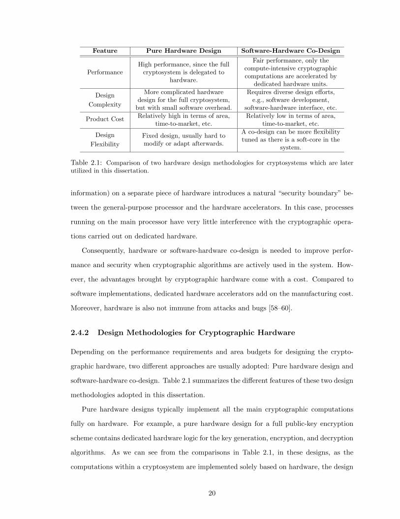
Feature Pure Hardware Design Software-Hardware Co-Design
PerformanceHigh performance, since the full
cryptosystem is delegated tohardware.
Fair performance, only thecompute-intensive cryptographiccomputations are accelerated by
dedicated hardware units.
Design
Complexity
More complicated hardwaredesign for the full cryptosystem,
but with small software overhead.
Requires diverse design efforts,e.g., software development,
software-hardware interface, etc.
Product Cost Relatively high in terms of area,time-to-market, etc.
Relatively low in terms of area,time-to-market, etc.
Design
Flexibility
Fixed design, usually hard tomodify or adapt afterwards.
A co-design can be more flexibilitytuned as there is a soft-core in the
system.
Table 2.1: Comparison of two hardware design methodologies for cryptosystems which are laterutilized in this dissertation.
information) on a separate piece of hardware introduces a natural “security boundary” be-
tween the general-purpose processor and the hardware accelerators. In this case, processes
running on the main processor have very little interference with the cryptographic opera-
tions carried out on dedicated hardware.
Consequently, hardware or software-hardware co-design is needed to improve perfor-
mance and security when cryptographic algorithms are actively used in the system. How-
ever, the advantages brought by cryptographic hardware come with a cost. Compared to
software implementations, dedicated hardware accelerators add on the manufacturing cost.
Moreover, hardware is also not immune from attacks and bugs [58–60].
2.4.2 Design Methodologies for Cryptographic Hardware
Depending on the performance requirements and area budgets for designing the crypto-
graphic hardware, two different approaches are usually adopted: Pure hardware design and
software-hardware co-design. Table 2.1 summarizes the different features of these two design
methodologies adopted in this dissertation.
Pure hardware designs typically implement all the main cryptographic computations
fully on hardware. For example, a pure hardware design for a full public-key encryption
scheme contains dedicated hardware logic for the key generation, encryption, and decryption
algorithms. As we can see from the comparisons in Table 2.1, in these designs, as the
computations within a cryptosystem are implemented solely based on hardware, the design
20

complexity, product cost, as well as time-to-market are relatively high. However, high costs,
on the other hand, bring us improved performance which may be desired in specific types
of applications. Nowadays, pure hardware designs are widely adopted in high-end cloud
server applications, e.g., machine learning accelerators implemented as a cloud service on
large servers.
Another approach that is also commonly adopted for designing cryptographic hardware
is software-hardware co-designs. For constructing software-hardware co-designs, the most
compute-intensive computations in the algorithm are first identified (e.g., by use of profil-
ing tools such as GNU gprof [61]). Once identified, dedicated hardware accelerators are
designed to speed up these operations. Apart from the hardware accelerators, a soft-core
is also needed in the system, which is usually a general-purpose processor such as an ARM
processor or a RISC-V CPU. Once the hardware accelerators are integrated into the sys-
tem, the workload of the cryptosystem can be divided into two parts: Compute-intensive
computations handled by dedicated hardware accelerators and the rest of the computations
remaining on the soft-core. Combining the flexibility of the soft-core and the performance
of dedicated hardware accelerators make the co-design an ideal design approach especially
for low-end embedded devices. These devices usually have very constrained resources; how-
ever, good performance is still desired when running cryptographic algorithms on these
platforms. In general, software-hardware co-designs bring a trade-off between performance
and hardware cost. Depending on the area budget, users can spend as much chip area as
they can afford in order to get the best performance out of the hardware constraints.
2.5 Hardware Platforms for Prototyping
After running simulation tests for cryptographic hardware, the functional correctness and
timing properties of the hardware design need to be further tested and verified on real hard-
ware platforms. In this section, we describe two hardware platforms used in this dissertation
that are widely used for prototyping hardware designs for cryptographic algorithms.
21

2.5.1 Field Programmable Gate Arrays
Field Programmable Gate Arrays (FPGAs) are semiconductor devices that are based around
an array of configurable logic blocks interconnected through programmable interconnects.
FPGAs can be reprogrammed for implementing desired functionalities or applications. The
reprogrammability feature distinguishes FPGAs from application specific integrated circuits
(described later in Section 2.5.2), which are customized for specific design tasks and cannot
be easily modified after being manufactured. The most common FPGA architecture con-
sists of an array of logic blocks, input and output pads, and interconnects. In general, a
logic block consists of a few logical cells in which each cell contains Look-Up-Tables (LUTs)
and Flip-Flops (FF). The detailed architecture of the logical cell depends on the manufac-
turer and the specific model of the FPGA. Apart from logic blocks, modern FPGA families
also contain hard blocks that provide efficient and ready-to-use embedded circuits in silicon.
These hard blocks can increase the speed and cost compared to building them from logical
primitives. For example, Digital Signal Processing (DSP) blocks can compute multiply-and-
add (MAC) operations efficiently and are used widely for multiplication-intensive applica-
tions. In addition to DSP blocks, in general FPGAs are also embedded with high-speed
input and output logic, memory blocks, PCI Express, DRAM controller, and so on.
For running hardware designs on an FPGA, the user first needs to provide her design
written in a hardware description language (HDL). The most common HDLs are Verilog,
VHDL and SystemVerilog. Before programming the FPGA with the hardware design, users
can first verify the functional correctness of the design by use of simulation tools. Once the
functional correctness of the hardware design is verified through simulation, the design is
further fed into an electronic design automation (EDA) tool. The EDA tool first generates
a netlist for the design, and then fits the design to the FPGA through the place-and-route
process. Further, a binary file is generated, typically using the FPGA vendor’s proprietary
software. The binary file is then used to configure or reconfigure the FPGA; afterwards,
user’s hardware design will be running on the FPGA.
Apart from the programmable logic in the FPGA fabric, many modern FPGAs also
have one or more hard processor cores in the system. For example, Xilinx Zynq-7000S
22

devices [62] feature a single-core ARM Cortex-A9 processor mated with 28nm Artix-7 based
programmable logic. The introduction of a hard processor core into the FPGA has made
the platform an ideal candidate in developing embedded applications. In addition to hard
processor cores, soft processor cores such as RISC-V can be instantiated in the FPGA fabric
to emulate a system on a chip where some computations are running on the soft processor
core and others are offloaded to the hardware accelerator.
In recent years, FPGAs have been applied for hardware acceleration, especially in ma-
chine learning applications where the computation workload is high. For accelerating ap-
plications in a larger scale, more and more FPGAs are being deployed in the cloud as well.
Nowadays, more and more companies are providing cloud FPGA services, e.g., Amazon
AWS F1, Microsoft Azure, and Huawei Cloud. The acceleration of applications by FPGA
and the unlimited capacities of the cloud are expected to be more and more pervasive in
the future.
2.5.2 Application Specific Integrated Circuits
Once hardware designs are verified and prototyped on FPGA platforms, these designs can
be further converted to Application Specific Integrated Circuits (ASICs). An ASIC is an
integrated circuit chip which is typically fabricated using metal-oxide-semiconductor (MOS)
technology, as a MOS integrated circuit chip. For smaller designs or lower production vol-
umes, FPGAs are usually more cost-effective; however, for very large production volumes,
ASICs are preferable despite the high non-recurring engineering cost. For manufacturing
ASICs, a hardware design written in HDL is first constructed, which is further verified to
ensure the functional correctness. Unlike most FPGAs, ASICs cannot be reprogrammed
once fabricated, thus ASIC designs need an intensive verification process for full test cov-
erage. The verified hardware design is then transformed through logic synthesis into a
large collection of lower-level constructs called standard cells. These cells are taken from a
standard-cell library consisting of pre-constructed logic gates performing specific functions.
The logic synthesis step generates a gate-level netlist containing the information of the re-
quired standard cells and the connections between them. This netlist file is then further fed
to the placement step, followed by the routing step.
23

2.5.3 FPGA Designs vs. ASIC Designs
Compared to FPGA designs, ASIC designs require a much higher fixed cost, namely the
non-recurring engineering cost. However, when produced in mass productions, this cost
is amortized, thus ASIC designs are commonly adopted when large volumes of production
is targeted. In terms of power consumption, ASIC designs are usually much more power
efficient than FPGAs. Further, ASIC designs fabricated using the same process can run
at much higher frequency compared to FPGAs since its circuit is optimized for its spe-
cific function. However, despite these performance and power advantages, ASIC designs
also have a few constraints. In general, the design complexity is much higher since ASIC
designers need to care for the back-end design (e.g., the reset tree, the clock tree, testing
constraints, etc) while FPGA designers do not need to. Another constraint lies in the flex-
ibility of the design. ASIC designs cannot be modified once it is taped-out into silicon. On
the contrary side, FPGAs are reconfigurable and users can reconfigurable the full circuit, or
part of the circuit, depending on the user needs. This feature makes FPGAs highly suited
for applications such as cell phone base stations [63] where the currently deployed algorithm
or hardware design needs to be upgraded frequently. Depending on the specific applications
and budgets, users can choose the best suited platform for their hardware designs.
24

Chapter 3
Code-based Cryptography: Classic
McEliece Cryptosystem on
Hardware
This chapter presents details of a pure hardware design for the Niederreiter cryptosystem
using binary Goppa codes, which is the equivalent of the Classic McEliece proposal sub-
mitted to the NIST PQC standardization process. The hardware design includes modules
for key generation, encryption, and decryption. This implementation is constant-time in
order to protect against timing based side-channel attacks. Further, the design is fully pa-
rameterized, using code-generation scripts, in order to support a wide range of parameter
choices for security, including binary field size, the degree of the Goppa polynomial, and the
code length. There are also performance related parameters that can be used to generate
different configurations for each security level. The parameterized design allows us to choose
design parameters for time-area trade-offs in order to support a wide variety of applications
ranging from smart cards to server accelerators.
3.1 Background
The first public-key encryption scheme based on coding theory was proposed in 1978 by
McEliece [32], known as the McEliece public-key cryptosystem. In 1986, Niederreiter pro-
25

posed a variant of the McEliece cryptosystem that uses a parity check matrix for encryption
instead of a generator matrix as used by McEliece. Furthermore, Niederreiter proposed to
use Reed-Solomon codes, which were later shown to be insecure [64]. However, the Nieder-
reiter cryptosystem using binary Goppa codes remains secure and the Niederreiter cryp-
tosystem has been shown to be equivalent (using corresponding security parameters) to the
McEliece cryptosystem [34].
The private key of the Niederreiter cryptosystem [33] is a binary Goppa code G that is
able to correct up to t errors in a n-bit codeword. It consists of two parts: A generator,
which is a monic irreducible polynomial g(x) of degree t over GF(2m), and a support, which
is a random sequence of n distinct elements from GF(2m). The public key is a binary parity
check matrix H ∈ GF(2)mt×n, which is uniquely defined by the binary Goppa code. To
reduce the size of the public key, the matrix H of size mt×n can be compressed to a matrix
K ∈ GF(2)mt×k of size mt × (n − mt) with k = (n − mt) by computing its systematic
form. This is often called “modern Niederreiter” [33] and can also be used for the McEliece
cryptosystem. For encryption, the sender encodes the message as a weight-t error vector e
of length n. Then e is multiplied with the public parity check matrix H and the resulting
syndrome is sent to the receiver as the ciphertext c. For decryption, the receiver uses the
secret support and the generator to decrypt the ciphertext in polynomial time using an
efficient syndrome decoding algorithm of G. If neither the support nor the generator is
known, it is computationally hard to decrypt the ciphertext, given only the public key H.
The Niederreiter cryptosystem with properly chosen parameters is believed to be secure
against attacks using quantum computers [3].
3.1.1 Related Work
Inspired by the confidence in the code-based cryptosystems, there are a few hardware imple-
mentations of different variants of these cryptosystems, e.g., [65–67]. Most of the work only
focuses on the encryption and decryption parts of the cryptosystem due to the complexity
of the key generation module. Moreover, none of the prior designs are fully configurable as
ours nor do they support the recommended “128-bit post-quantum security” level. We are
aware of only one publication [67] that provides the design of the McEliece cryptosystem
26

including key generation, encryption and decryption modules. However, their design only
provides a 103-bit classical security level, which does not meet the currently recommended
security level for defending against quantum computers. More importantly, the design
in [67] is not constant-time and has potential security flaws. For example, within their
key generation part, they generate non-uniform permutations, and within the decryption
part, they implement a non-constant-time decoding algorithm. Note that our work focuses
on a design that can defend against timing side-channel attacks due to its constant-time
implementation. However, other types of side-channel attacks are out of scope of this work.
3.1.2 Motivation for Our Work
The Niederreiter cryptosystem has proven to be one of the most confidence-inspiring can-
didates among all the NIST PQC candidates. However, the large security parameters of
the complex Niederreiter cryptosystem make it particularly troublesome for use in embed-
ded systems (due to strong restrictions on resource usage) and in server scenarios (given a
large number of simultaneous connections). In this chapter, we demonstrate that hardware
acceleration can help to improve the performance – either by providing a low-area, power
efficient cryptographic core in the embedded scenario or by providing a large, latency or
throughput optimized cryptographic accelerator for the server scenario. The hardware ac-
celeration is demonstrated using design realized on an FPGA. The FPGA implementation
can be tuned in regard to performance and resource usage for either low-resource usage in
embedded systems or high performance as accelerator for servers.
Furthermore, we provide a generic implementation that can be used for different perfor-
mance parameters. This enables us to synthesize our design for the different sets of security
parameters included in the third round submission of the “Classic McEliece” proposal to
the NIST process. For a given set of parameters, i.e. security level, the design can be
further configured to trade-off performance and area, by changing widths of data paths,
memories, and other parameters inside the design, without affecting the security level. All
of the parameters can be configured for key generation, encryption, and decryption.
This chapter is based on our publications [68–71] and our “Classic McEliece” submis-
sion [3] to the third round of the NIST PQC standardization process. The contributions
27

and organizations of this chapter are as follows:
• We explain the key generation, encryption, and decryption algorithms in the Nieder-
reiter cryptosystem in Section 3.2.
• We present efficient hardware implementations for the binary finite field arithmetic
and polynomial arithmetic in Section 3.3.
• Based on these arithmetic units, we further design, implement, and evaluate the fol-
lowing functional blocks that are used to accelerate the most compute-intensive op-
erations in the cryptosystem, including: A Gaussian systemizer which works for any
large-sized matrix over any binary field (described in Section 3.4), a novel polynomial
multiplier based on the Gao-Mateer additive FFT algorithm (described in Section 3.5),
two new random permutation units based on Fisher-Yates shuffle and merge sort re-
spectively (described in Section 3.6), as well as an efficient decoding unit based on the
Berlekamp-Massey algorithm (described in Section 3.7).
• Then in Section 3.8 these high-level functional blocks are used to build the complete
cryptosystem, including the key generation, encryption, and decryption units. Our
work is the first that presents a post-quantum secure, constant-time, efficient, and
tunable FPGA-based implementation of the Niederreiter cryptosystem using binary
Goppa codes.
• We present methods for thoroughly testing the hardware design in Section 3.9. The
evaluation results presented in in Section 3.10 and the comparison results with re-
lated work in Section 3.11 successfully demonstrate the practicability and efficiency
of running the complex Niederreiter cryptosystem on real FPGA platforms.
• In the end, a short summary for this chapter is given in Section 3.12.
3.2 Classic McEliece and the Niederreiter Cryptosystem
The Niederreiter cryptosystem consists of three operations: Key generation, encryption,
and decryption.
28
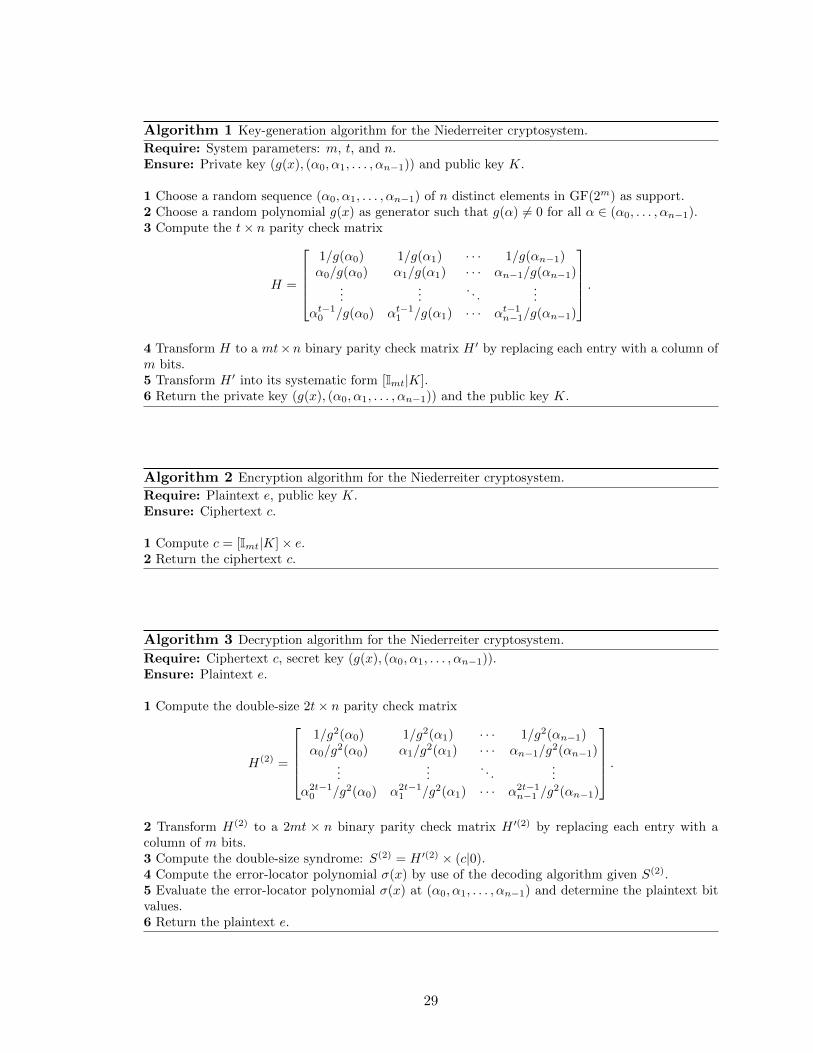
Algorithm 1 Key-generation algorithm for the Niederreiter cryptosystem.
Require: System parameters: m, t, and n.Ensure: Private key (g(x), (α0, α1, . . . , αn−1)) and public key K.
1 Choose a random sequence (α0, α1, . . . , αn−1) of n distinct elements in GF(2m) as support.2 Choose a random polynomial g(x) as generator such that g(α) 6= 0 for all α ∈ (α0, . . . , αn−1).3 Compute the t× n parity check matrix
H =
1/g(α0) 1/g(α1) · · · 1/g(αn−1)α0/g(α0) α1/g(α1) · · · αn−1/g(αn−1)
......
. . ....
αt−10 /g(α0) αt−11 /g(α1) · · · αt−1n−1/g(αn−1)
.
4 Transform H to a mt×n binary parity check matrix H ′ by replacing each entry with a column ofm bits.5 Transform H ′ into its systematic form [Imt|K].6 Return the private key (g(x), (α0, α1, . . . , αn−1)) and the public key K.
Algorithm 2 Encryption algorithm for the Niederreiter cryptosystem.
Require: Plaintext e, public key K.Ensure: Ciphertext c.
1 Compute c = [Imt|K]× e.2 Return the ciphertext c.
Algorithm 3 Decryption algorithm for the Niederreiter cryptosystem.
Require: Ciphertext c, secret key (g(x), (α0, α1, . . . , αn−1)).Ensure: Plaintext e.
1 Compute the double-size 2t× n parity check matrix
H(2) =
1/g2(α0) 1/g2(α1) · · · 1/g2(αn−1)α0/g
2(α0) α1/g2(α1) · · · αn−1/g
2(αn−1)...
.... . .
...α2t−10 /g2(α0) α2t−1
1 /g2(α1) · · · α2t−1n−1 /g
2(αn−1)
.
2 Transform H(2) to a 2mt × n binary parity check matrix H ′(2) by replacing each entry with acolumn of m bits.3 Compute the double-size syndrome: S(2) = H ′(2) × (c|0).4 Compute the error-locator polynomial σ(x) by use of the decoding algorithm given S(2).5 Evaluate the error-locator polynomial σ(x) at (α0, α1, . . . , αn−1) and determine the plaintext bitvalues.6 Return the plaintext e.
29

3.2.1 Key Generation
Key generation is the most expensive operation; it is described in Algorithm 1. The system
parameters are: m, the size of the binary field, t, the number of correctable errors, and n,
the code length. Code rank k is determined as k = n −mt. Step 2 of the key-generation
algorithm is implemented by computing an irreducible Goppa polynomial g(x) of degree t as
the minimal polynomial of a random element r from a polynomial ring over GF(2m) using a
power sequence 1, r, . . . , rt and Gaussian systemization in GF(2m) (see Section 3.8.1). Step 3
requires the evaluation of g(x) at points {α0, α1, . . . , αn−1}. To achieve high efficiency, we
follow the approach of [72] which evaluates g(x) at all elements of GF(2m) using a highly
efficient additive FFT algorithm (see Section 3.5). By use of this algorithm, we evaluate
g(x) at all α ∈ GF(2m) and then choose the required αi by computing a random sequence
(α0, α1, . . . , αn−1) from a permuted list of indices P . In Section 3.6, two different approaches
for generating a random permutation are presented. For Step 5, we use an efficient Gaussian
systemization module for matrices over GF(2) (see Section 3.4).
3.2.2 Encryption
Within the Niederreiter cryptosystem, the ciphertext is defined as a syndrome, which is the
product between the parity check matrix and the plaintext. As shown in Algorithm 2, the
encryption operation is very simple and maps to the multiplication between the extended
public key [Imt|K] and the plaintext e. In our work, we only focus on the core functionalities
of the Niederreiter cryptosystem, therefore we assume that the input plaintext e is an n-bit
error message of weight t.
3.2.3 Decryption
As shown in Algorithm 3, the decryption operation starts from extracting the error locator
polynomial out of the ciphertext using a decoding algorithm. Patterson’s algorithm [73] and
Berlekamp-Massey’s [74] algorithm are two of the most standard algorithms for decoding.
We use the Berlekamp-Massey’s (BM) algorithm [74] in our design since it generalizes to
algebraic list-decoding algorithms more easily than Patterson’s algorithm [73], and more
30

Param. Description Size (bits) Config. Description Size (bits)m Size of the binary field 13 g(x) Goppa polynomial 120× 13t Correctable errors 119 P Permutation indices 8192× 13n Code length 6960 H Parity check matrix 1547× 6960k Code rank 5413 K Public key 1547× 5413
Table 3.1: Parameters and resulting configuration for the Niederreiter cryptosystem.
importantly, it is easier to protect against timing side-channel attacks. A dedicated BM
module is designed for decoding, as described in Section 3.7. One problem within BM-
decoding is that it can only recover t2 errors. To solve this issue, we use the trick proposed
by Nicolas Sendrier [65]. We first compute the double-size parity check matrix H(2) cor-
responding to g2(x), then we append (n − mt) zeros to c. Based on the fact that e and
(c|0) belong to the same coset given H(2) × (c|0) = H × e, computing the new double-size
syndrome S(2) enables the BM algorithm to recover t errors. Once the error locator poly-
nomial is computed, it is evaluated at the secret random sequence (α0, α1, . . . , αn−1), and
finally the plaintext e is recovered.
3.2.4 Security Parameters
The PQCRYPTO project [75] gives “initial recommendations” for several PQC schemes.
For McEliece and Niederreiter using binary Goppa codes, they recommend to use a binary
field of size m = 13, adding t = 119 errors, code length n = 6960, and code rank k =
n−mt = 6960−13 ·119 = 5413 for “128-bit post-quantum security” [76]. These parameters
were chosen to provide maximum security for a public key size of at most 1 MB [77].
This parameter set (n, k, t) = (6960, 5413, 13) is also included and recommended for use
in the third round NIST submission of “Classic McEliece” [3], as one of the parameter
sets targeting the highest NIST security level (i.e., security level 5) [78]. We use these
recommended parameters shown in Table 3.1 as primary target for our implementation.
However, since our design is fully parameterized, we can synthesize our implementation for
any meaningful choice of m, t, n, and k for comparison with prior art (see Section 3.10).
31

Algorithm Logic Reg. Fmax (MHz)
Schoolbook Algorithm 90 78 6372-split Karatsuba Algorithm 99 78 6253-split Karatsuba Algorithm 101 78 529Bernstein 87 78 621
Table 3.2: Performance of different field multiplication algorithms for GF(213).
3.3 Field Arithmetic
The lowest-level building blocks in our implementation are GF(2m) finite field arithmetic
and on the next higher level GF(2m)[x]/f polynomial arithmetic.
3.3.1 GF(2m) Finite Field Arithmetic
GF(2m) represents the basic finite field in the Niederreiter cryptosystem. Our code for
all the hardware implementations of GF(2m) operations is generated by code-generation
scripts, which take in m as a parameter and then automatically generate the corresponding
Verilog HDL code.
GF(2m) Addition. In GF(2m), addition corresponds to a simple bitwise xor operation of
two m-bit vectors. Therefore, each addition has negligible cost and can often be combined
with other logic while still finishing within one clock cycle, e.g., a series of additions or
addition followed by multiplication or squaring.
GF(2m) Multiplication. Multiplication over GF(2m) is one of the most used opera-
tions in the Niederreiter cryptosystem. A field multiplication in GF(2m) is composed of
a multiplication in GF(2)[x] and a reduction modulo f , where f is a degree-m irreducible
polynomial. For the case of m = 13, we use the pentanomial f(x) = x13+x4+x3+x+1 since
there is no irreducible trinomial of degree 13. We are using plain schoolbook multiplication,
which turns out to deliver good performance. Table 3.2 shows that the schoolbook version
of GF(213) multiplication achieves a higher maximum frequency, Fmax, while requiring less
logic compared to several of our implementations using Karatsuba multiplication [79, 80].
We combine multiplication in GF(2)[x] and reduction modulo f such that one GF(2m)
multiplication only takes one clock cycle.
32

GF(2m) Squaring. Squaring over GF(2m) can be implemented using less logic than
multiplication and therefore an optimized squaring module is valuable for many applications.
However, in the case of the Niederreiter algorithm, we do not require a dedicated squaring
module since an idle multiplication module is available in all cases when we require squaring.
Squaring using GF(2m) multiplication takes one clock cycle.
GF(2m) Inversion. Inside the GF(2m) Gaussian systemizer, elements over GF(2m) need
to be inverted. An element a ∈ GF(2m) can be inverted by computing a−1 = a|GF(2m)|−2
following Fermat’s little theorem [81]. This can be done with a logarithmic amount of
squarings and multiplications. For example, inversion in GF(213) can be implemented using
twelve squarings and four multiplications. However, this approach requires at least one
multiplication circuit (repeatedly used for multiplications and squarings) plus some logic
overhead and has a latency of at least several cycles in order to achieve high frequency.
Therefore, we decided to use a pre-computed lookup table for the implementation of the
inversion module. For inverting an element α ∈ GF(2m), we interpret the bit-representation
of α as an integer value and use this value as the address into the lookup table. For
convenience, we added an additional bit to each value in the lookup table that is set high in
case the input element α can not be inverted, i.e., α = 0. This saves additional logic that
otherwise would be required to check the input value. Thus, the lookup table has a width
of m+1 and a depth of 2m, and each entry can be read in one clock cycle. The lookup table
is read-only and therefore can be stored in either read-only memory or logic resources.
3.3.2 GF(2m)[x]/f Polynomial Arithmetic
GF(2m)[x]/f is an extension field of GF(2m). Elements in this extension field are repre-
sented by polynomials with coefficients in GF(2m) modulo an irreducible polynomial f . We
are using a sparse polynomial for f , e.g., the trinomial x119 + x8 + 1, in order to reduce the
cost of polynomial reduction.
Polynomial Addition. The addition of two degree-d polynomials with d + 1 coefficients
is equivalent to pair-wise addition of the coefficients in GF(2m). Therefore, polynomial
33

Algorithm Mult. Cycles Logic Time×Area Fmax (MHz)
1-level Karatsuba 17×(20×20) 20 377 11, 860 4.47 · 106 3422-level Karatsuba 17×17×(4×4) 16 632 12, 706 8.03 · 106 1512-level Karatsuba 17×17×(4×4) 4 1788 11, 584 2.07 · 107 254
Table 3.3: Performance of different multiplication algorithms for degree-118 polynomials.
addition can be mapped to an xor operation on two m(d+ 1)-bit vectors and it can be
performed in one clock cycle.
Polynomial Multiplication. Due to the relatively high cost of GF(2m) multiplication
compared to GF(2m) addition, for polynomials over GF(2m) Karatsuba multiplication [79]
is more efficient than classical schoolbook multiplication in terms of logic cost when the
size of the polynomial is sufficiently large. Given two polynomials A(x) =∑5
i=0 aixi and
B(x) =∑5
i=0 bixi, schoolbook polynomial multiplication can be implemented in hardware
as follows: Calculate (a5b0, a4b0, . . . , a0b0) and store the result in a register. Then similarly
calculate (a5bi, a4bi, . . . , a0bi), shift the result left by i · m bits, and then add the shifted
result to the register contents, repeat for all i = 1, 2, . . . , 5. Finally, the result stored in
the register is the multiplication result (before polynomial reduction). One can see that
within this process, 6 × 6 GF(2m) multiplications are needed. Karatsuba polynomial mul-
tiplication requires fewer finite-field multiplications compared to schoolbook multiplication.
For the above example, Montgomery’s six-split Karatsuba multiplication [80] requires only
17 field element multiplications over GF(2m) at the cost of additional finite field additions
which are cheap for binary field arithmetic. For large polynomial multiplications, usually
several levels of Karatsuba are applied recursively and eventually on some low level school-
book multiplication is used. The goal is to achieve a trade-off between run-time and logic
overhead.
The multiplication of two polynomials of degree d = t − 1 is a key step in the key-
generation process for computing the Goppa polynomial g(x). Table 3.3 shows the results of
several versions of polynomial multiplication for t = 119, i.e., d = 118, using parameterized
six-split Karatsuba by adding zero-terms in order to obtain polynomials with 120 and 24 co-
efficients respectively. On the lowest level, we use parameterized schoolbook multiplication.
The most efficient approach for the implementation of degree-118 polynomial multiplica-
34

tion turned out to be one level of six-split Karatsuba followed by schoolbook multiplication,
parallelized using twenty GF(213) multipliers. Attempts using one more level of six-split
Karatsuba did not notably improve area consumption (or even worsened it) and resulted
in both more cycles and lower frequency. Other configurations, e.g., five-split Karatsuba
on the second level or seven-split Karatsuba on the first level, might improve performance,
but our experiments do not indicate that performance can be improved significantly. In
the final design, we implemented a one-level six-split Karatsuba multiplication approach,
which uses a size-dd+16 e schoolbook polynomial multiplication module as its building block.
It only requires 377 cycles to perform one multiplication of two degree-118 polynomials.
These arithmetic units are further used for constructing functional blocks, which are
main building blocks within the Niederreiter cryptosystem (as shown in Figure 3.7). In the
following sections, we will present the following functional blocks: Two Gaussian systemizers
for matrix systemization over GF(2) and GF(2m) respectively (in Section 3.4), Gao-Mateer
additive FFT for polynomial evaluations (in Section 3.5), two different random permutation
units for generating uniformly distributed permutations (in Section 3.6), and a Berlekamp-
Massey module for decoding (in Section 3.7).
3.4 Gaussian Systemizer for Gaussian Elimination
Solving systems of linear equations (SLEs) is an important computational task in many
scientific fields. Solving systems over binary fields is of particular interest in cryptography
and cryptanalysis. It is also an important step in the key generation of the Niederreiter
cryptosystem [33]. Building systolic architectures for Gaussian elimination is a standard ap-
proach for solving SLEs in hardware. Most of the existing publications [82–84] target small-
(about 10 × 10 elements) to medium-sized (about 50 × 50 elements) matrices by building
a large systolic architecture that matches the matrix size. Due to resource limitations on
FPGAs, such designs are not suitable for large matrices (over 200× 200 elements) as there
are not enough FPGA resources. In our work, we efficiently break the Gaussian elimination
process into a number of steps and phases that use a systolic architecture, which is smaller
than the matrix size, to perform operations on the original, large matrix.
35

P11 P12 P13. . . P1l
P22 P23. . . P2l
P33. . . .... . .
...
Pll
Figure 3.1: Systolic array of processor elements from [85].
3.4.1 Gaussian Elimination
Gaussian elimination is a basic method that can be extended and used for, among others,
solving systems of linear equations, bringing a matrix into its systematic form, or performing
matrix inversions. Consider solving a system of linear equations in the form A · x = b,
where A is a square matrix and b is a vector. First, Gaussian elimination is used to
transform the system into its equivalent form U ·x = b′, where U is an upper right triangular
matrix. The transformation is done by a sequence of elementary row operations. Once
U · x = b′ is obtained, the system is solved by using backward substitution, i.e., elementary
row operations are applied that convert the system to I · x = b′′, where I is an identity
matrix and b′′ is the solution to this system.
For matrix systemization, a rectangular matrix G (of size l×k, k > l) is divided into the
left square part G1 (of size l× l) and the right part G2 (of size l× (k − l)). By performing
Gaussian elimination and backward substitution on the whole matrix, its left part is reduced
to the identity matrix I while its right part is converted to a matrix P . Thus, G is brought
to its systematic form G = [I|P ].
3.4.1.1 Systolic Architectures for Gaussian Elimination
Hardware architectures for Gaussian elimination over finite fields can be divided into three
types: Systolic array, systolic network, and systolic line.
Systolic Array. In 1989, Hochet, Quinton, and Robert introduced a systolic array of
processors for doing Gaussian elimination on a matrix over GF(p) with partial pivoting [85].
36
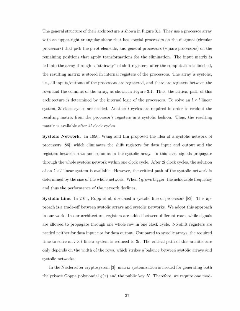
The general structure of their architecture is shown in Figure 3.1. They use a processor array
with an upper-right triangular shape that has special processors on the diagonal (circular
processors) that pick the pivot elements, and general processors (square processors) on the
remaining positions that apply transformations for the elimination. The input matrix is
fed into the array through a “stairway” of shift registers; after the computation is finished,
the resulting matrix is stored in internal registers of the processors. The array is systolic,
i.e., all inputs/outputs of the processors are registered, and there are registers between the
rows and the columns of the array, as shown in Figure 3.1. Thus, the critical path of this
architecture is determined by the internal logic of the processors. To solve an l × l linear
system, 3l clock cycles are needed. Another l cycles are required in order to readout the
resulting matrix from the processor’s registers in a systolic fashion. Thus, the resulting
matrix is available after 4l clock cycles.
Systolic Network. In 1990, Wang and Lin proposed the idea of a systolic network of
processors [86], which eliminates the shift registers for data input and output and the
registers between rows and columns in the systolic array. In this case, signals propagate
through the whole systolic network within one clock cycle. After 2l clock cycles, the solution
of an l × l linear system is available. However, the critical path of the systolic network is
determined by the size of the whole network. When l grows bigger, the achievable frequency
and thus the performance of the network declines.
Systolic Line. In 2011, Rupp et al. discussed a systolic line of processors [83]. This ap-
proach is a trade-off between systolic arrays and systolic networks. We adopt this approach
in our work. In our architecture, registers are added between different rows, while signals
are allowed to propagate through one whole row in one clock cycle. No shift registers are
needed neither for data input nor for data output. Compared to systolic arrays, the required
time to solve an l × l linear system is reduced to 3l. The critical path of this architecture
only depends on the width of the rows, which strikes a balance between systolic arrays and
systolic networks.
In the Niederreiter cryptosystem [3], matrix systemization is needed for generating both
the private Goppa polynomial g(x) and the public key K. Therefore, we require one mod-
37

ule for Gaussian systemization of matrices over GF(2) and one module for matrices over
GF(2m). In the following sections, we first present the Gaussian systemizer over GF(2),
then we show how to get a modified version for Gaussian systemizer over GF(2m).
3.4.2 GF (2) Guassian Systemizer
A key design and implementation detail is the size of the systolic architecture compared
to the size of the matrix. Most existing designs [82–84] focus on small- and medium-sized
matrices, as for those sizes the systolic architecture can fully fit on the FPGA. Meanwhile, as
mentioned in the text above, using one large systolic architecture to do Gaussian elimination
on large matrices is not practical due to the resource limitations of FPGAs.
Instead of processing the input matrix on the whole, prior work [87] proposes operating
on column blocks of the input matrix. Their design uses two systolic processor arrays, TRI-
SA and SQR-SA, to simulate the functionality of the original large array by storing and
replaying the outputs of the processor arrays accordingly. A classical (software) implemen-
tation of Gaussian elimination sequentially picks a single row as pivot row and eliminates
the entries in the corresponding column of the remaining rows. The design in [87] picks a
block of n rows at once and eliminates the corresponding columns all together.
The architecture in [87] is composed of two basic processor elements: processor A and
processor B, similar to the design in [85]. The processor array TRI-SA has an upper-
right diagonal shape similar to the original processor array from [85] (see Figure 3.1). It
contains processor A elements that are in charge of computing the pivot elements for
the elimination and processor B elements that apply (together with processor A) the
row transformations necessary for elimination. The processor array SQR-SA contains only
processor B elements. It is used to perform the row operations on the remaining column
blocks of the matrix, as defined by the outputs of TRI-SA.
The design in [87] divides the system-solving process into two passes of Gaussian elimina-
tion: One for triangularization (forward elimination) and one for systemization (backward
elimination). It iteratively uses the two processor arrays TRI-SA and SQR-SA to process
corresponding matrix column blocks. After the first pass, the left part of the matrix is
eliminated into an upper-right triangular matrix where the diagonal elements are all one.
38

ABr
Br
Br
. . .
Br
Br
ABr
Br
. . .
Br
Br
Br
ABr
. . .
Br
. . .
. . .
. . .
. . .
. . .
Br
Br
Br
. . .
ABr
Figure 3.2: Layout of module comb SA. Input function A to the processor AB s is not shown.Registers are shown as boxes on the wires connecting processors.
After the second pass, the partially eliminated matrix is flipped and then eliminated in a
similar way as during the first operation. After this second elimination, the left part of the
matrix is turned into the identity matrix and the linear system is completely solved.
Our design is based on [85] and improves upon [87]. We use a similar notation as [87]
whenever possible in order to simplify comparison. We improve the prior design by com-
bining TRI-SA and SQR-SA into one square module comb SA which has diagonal processor
elements that can be used either as processor A or processor B. These processor elements
are called processor AB. This approach allows us to save about 1/3 of the logic required
by [87] for TRI-SA and SQR-SA. Figure 3.2 shows the design details of our new comb SA
module. Similar to [87], our algorithm uses several phases where in each phase n pivoting
rows are picked at once. Each phase then requires several steps in order to perform the
required row operations on all column blocks. To simplify this process, we store the matrix
in a column-block format in the on-chip block memory. To enable a wide range of applica-
tions, our design is parameterized: The block size n can be freely chosen, e.g., small in order
to reduce resources, large in order to reduce computing time, or according to the memory
architecture in case the word size of the memory is fixed. Furthermore, the number of rows
(l) and columns (k, where k ≥ l) can be set as needed. For simplification, both l and k
must be multiples of n; otherwise l and k are simply rounded up to the next multiple of n.
Hardware Implementation. Our design of the GF (2) Gaussian systemizer is imple-
39

5 10 20 40 80 160 320 64012801
1.2
1.4
1.6
1.8
2
nQ
uoti
ent
ofC
ycl
eC
ou
nts k = l
k = 2lk = 4l
Figure 3.3: Quotient of the dual-pass systolic line approach divided by our single-pass systolic lineapproach (l = 1280).
mented in a hierarchical way: Processors of type processor AB and processor B consist
the core logic. These processors are organized in an n× n array structure within the mod-
ule comb SA. The module comb SA is instantiated in the module step that computes the
elimination on one column block of width n. In turn, step is instantiated in the module
phase that computes the elimination of a certain row block for all remaining column blocks.
Finally, phase is instantiated within the module systemize that uses phase repeatedly in
order to eliminate all row blocks.
Comparison of Single-Pass and Dual-Pass Variants. The algorithm in [87] computes
the reduced row echelon form of the input matrix by applying a systolic array design for
Gaussian elimination twice in two passes. In both passes, the number of processed rows
decreases by n in each phase. This approach is also possible for our systolic line design. We
now show that our single-pass approach that operates on all l rows in each phase is more
efficient than a dual-pass approach that operates on n rows less in each phase.
In the dual-pass case, the first phase of Gaussian elimination processes the whole matrix.
In this phase, each step takes l + 2n clock cycles to finish processing its corresponding n-
column block of l rows. After this phase, n rows are in the desired triangular form. For the
second phase, since there are n rows less to process, each step requires only (l−n)+2n = l+n
cycles. Iteratively, the steps in phase i each require n cycles less compared to steps in the
previous phase i− 1, i.e., (l − in) + 2n cycles. Phase i requires kn − i steps. Thus in total,
40

5 10 20 40 80 160
300
400
500
n
Fm
ax
(MH
z)
matrix size: 320× 640
Figure 3.4: Maximum clock frequency (Fmax) achieved for different choices of n.
it takes 2 ·∑ l
n−1
i=0 (l+ 2n− in)( kn − i) clock cycles to compute the reduced row echelon form
using two passes.
Our design performs both forward and backward elimination in one single pass. The first
phase processes l rows of data which takes l+ 2n clock cycles. In each phase, all l rows are
reduced with respect to the current pivot rows. Therefore, in the second phase (as well as all
following phases), we need all l rows of data as input. Thus, in our design, each step takes a
fixed number of l+ 2n cycles. The first phase requires kn steps; thereafter, each phase takes
one step less compared to the previous phase. In total, we require∑ l
n−1
i=0 (l+2n)( kn−i) clock
cycles (plus a few cycles of overhead due to pipelining) in order to compute the reduced
row echelon form.
Figure 3.3 shows the theoretical analysis of the cycle count for the two variants for
different sizes of n. Our single-pass systolic line approach is always better compared to a
dual-pass systolic line approach in terms of number of cycles, especially when the matrix is
almost square. However, the dual-pass approach detects if the matrix is invertible already
after its first pass of the Gaussian elimination. Our single-pass approach needs to finish the
whole process first. Therefore, the dual-pass approach is a better choice when the matrix
is not guaranteed or known to be invertible and when an early abort of the system solving
is beneficial.
Trade-off between Area and Time. In our systolic line design, there is a trade-off
between area and time, controlled by the width n of comb SA. Bigger n means higher
41

Design n l kClock Fmax Runtime
ALMsa Slicesa Reg. FPGACycles (MHz) (ms)
[83] 50 50 50 150 150 0.00100 (3,106) 3,713 2,574 Spartan 3[84] 50 50 50 50 –d –d (9,256) 11,065 –d Spartan 3[82] 50 50 50 100e 300 0.00033e (3,349) 4,004 –d Spartan 3our 50 50 50 150 178 0.00084 3,129 5,236 Spartan 3our 50 50 50 150 413 0.00003 2,618 5,725 Stratix V
[87] 11 550 2,048 5,323,450c –d –d –d –d –d Virtex 5our 11 550 2,048 4,624,100b 305 15b 246 538 Virtex 5our 11 550 2,048 4,624,100b 332 14b 437 613 Stratix V
a Conversion from Xilinx Spartan 3 Slices to Altera Stratix V ALMs: 1 ALM = 3,129 / 2,618 ≈ 1.2 Slices.b Theoretical calculation, does not take into account a few cycles of overhead.c Theoretical calculation based on design description. d Exact information not provided in reference.e Average depending on input matrix.
Table 3.4: Comparison with existing FPGA implementations of Gaussian elimination.
parallelism and less computing time, but at the same time more logic. As mentioned
before, the critical path in our architecture is determined by the width of the rows of
comb SA. Figure 3.4 shows that the maximum clock frequency (Fmax) drops as the size of
the systolic line architecture (n) grows because of the longer routing paths on the FPGA.
However, for moderately large n up to n ≤ 80, Fmax can be kept above 400MHz, while for
n = 160, a relatively high Fmax of 360MHz can be maintained as well. Since we are using
a small- to medium-sized systolic line architecture when processing large-sized matrices,
logic utilization is no longer a constraint compared to the standard designs discussed in
literature. Instead, the available on-chip memory determines the largest size of the matrix
that can be processed by our design. Even larger matrices can be processed when using
off-chip memory.
Performance Evaluation and Comparison with Related Work. Table 3.4 presents
a comparison of performance and resource usage of our design with the GSMITH design
in [83], the systolic network design in [84], and the SMITH design in [82]. These designs
perform Gaussian elimination for medium-sized matrices; their processor array has the same
size as the input matrix. Our design is not intended for matrices of this size but optimized
for iterative operation on large matrices. To achieve a fair comparison, we compare only
our comb SA module using a processor array of a similar size to their designs. The resource
usage of [84] and [82] is only provided for Spartan 3 FPGAs. Therefore, we synthesized
42

our comb SA design for this FPGA. Compared with these three designs, our design achieves
very good performance in terms of frequency, area, and total runtime.
Shoufan et al. in [87] compute on large matrices of size 550 × 2, 048. They implement
a complete cryptosystem and do not provide details on the performance of their system
solver. In order to compare our design with [87], we calculated the expected number of
clock cycles for their design based on their description. Since we use a single-pass systolic
line approach, while they use a dual-pass systolic array approach, our design takes less clock
cycles to finish the elimination process. Since no performance and resource usage data is
provided for this part in their paper, no detailed comparison can be made.
3.4.3 GF (2m) Gaussian Systemizer
The Gaussian systemizer design above only supports systemization of matrices over GF(2).
In the Niederreiter cryptosystem, Gaussian eliminations on matrices over GF(2m) are also
needed in the key generation operation. In terms of hardware implementations, the GF (2m)
Gaussian systemizer works in a very similar fashion as the one over GF (2). The only
complexity sits at the matrix element elimination step where eliminating elements over
GF (2) simply translates to single-bit xor operations while relatively complex binary-field
multiplication and inversion operations are needed for eliminating elements over GF (2m).
Therefore, to achieve a Gaussian systemizer that can be applied to general binary fields,
we apply an important modification to the GF (2) Gaussian systemizer: We add a binary-
field inverter to the diagonal “pivoting” elements of the processor array and binary-field
multipliers to all the processors. Here, we use the single-cycle GF (2m) field multiplier as
described in Section 3.3. For the inverter, we adopt the GF(2m) field inversion unit (also
as described in Section 3.3) which is based on a lookup table. As we can easily see, both
the binary-field multiplier and the binary-field inverter finish computations within one clock
cycle. Therefore, both the GF (2m) field multiplier and the GF (2m) field inverter can be
integrated easily to the architecture of the existing GF (2) Gaussian systemizer. On the
other hand, the introduction of a field multiplier as well as a field inverter to the Gaussian
Systemier results in a larger resource requirement compared to the GF(2) version. However,
the longest path of the design still remains within the memory module in the Gaussian
43

systemizer and not within the computational logic for computations on large matrices.
Therefore, both Gaussian systemizers are able to run at relatively high frequencies.
3.5 Gao-Mateer Additive FFT Based Polynomial Multiplier
Evaluating a polynomial g(x) =∑t
i=0 gixi at n data points over GF(2m) is an essential step
in both the key generation and the decryption processes in the Niederreiter cryptosystem.
In key generation, evaluation of the Goppa polynomial g(x) is needed for computing the
parity check matrix H; while for decryption, it is required by the computation of the double-
size parity check matrix H(2) as well as the evaluation of the error locator polynomial σ(x).
Therefore, having an efficient polynomial-evaluation module is very important for ensuring
the performance of the overall design.
Schoolbook Algorithm: Horner’s Rule. Applying Horner’s rule is a common approach
for polynomial evaluation. For example, a polynomial f(x) =∑7
i=0 fixi of degree 7 can be
evaluated at a point α ∈ GF(2m) using Horner’s rule as
f(α) = f7α7 + f6α
6 + · · ·+ f1α+ f0
= (((f7α+ f6)α+ f5)α+ f4) . . . )α+ f0
using 7 field additions and 7 field multiplications by α. More generically speaking, one
evaluation of a polynomial of degree d requires d additions and d multiplications. Evaluating
several points scales linearly and is easy to parallelize. The asymptotic time complexity of
polynomial evaluation of a degree-d polynomial at n points using Horner’s rule is O(n · d).
3.5.1 Gao-Mateer Characteristic-2 Additive FFT Algorithm
In order to reduce this cost, we use a characteristic-2 additive FFT algorithm introduced
in 2010 by Gao and Mateer [88], which was used for multipoint polynomial evaluation by
Chou in 2013 [72]. This algorithm evaluates a polynomial at all elements in the field GF(2m)
using a number of operations logarithmic in the length of the polynomial. Most of these
operations are additions, which makes this algorithm particularly suitable for hardware
implementations. The asymptotic time complexity of additive FFT is O(2m · log2 (d)
).
44

The basic idea of this algorithm is to write f in the form f(x) = f (0)(x2+x)+xf (1)(x2+
x), where f (0)(x) and f (1)(x) are two half-degree polynomials, using radix conversion. The
form of f shows a large overlap between evaluating f(α) and f(α + 1). Since (α + 1)2 +
(α+ 1) = α2 + α for α ∈ GF(2m), we have:
f(α) = f (0)(α2 + α) + αf (1)(α2 + α)
f(α+ 1) = f (0)(α2 + α) + (α+ 1)f (1)(α2 + α).
Once f (0) and f (1) are evaluated at α2 + α, it is easy to get f(α) by performing one field
multiplication and one field addition. Now, f(α+1) can be easily computed using one extra
field addition as f(α+ 1) = f(α) + f (1)(α2 +α). Additive FFT applies this idea recursively
until the resulting polynomials f (0) and f (1) are 1-coefficient polynomials (or in another
word, constants). During the recursive operations, in order to use the α and α + 1 trick,
a twisting operation is needed for all the subspaces, which is determined by the new basis
of f (0) and f (1). Finally, the 1-coefficient polynomials of the last recursion step are used to
recursively evaluate the polynomial at all the 2m data points over GF(2m) in a concluding
reduction operation.
Radix Conversion. Radix conversion converts a polynomial f(x) of coefficients in GF(2m)
into the form of f(x) = f (0)(x2 + x) + xf (1)(x2 + x). As a basic example, consider a
polynomial f(x) = f0 + f1x + f2x2 + f3x
3 of 4 coefficients with basis {1, x, x2, x3}. We
compute the radix conversion as follows: Write the coefficients as a list [f0, f1, f2, f3]. Add
the 4th element to the 3rd element and add the new 3rd element to the 2nd element to obtain
[f0, f1 + f2 + f3, f2 + f3, f3]. This transforms the basis to {1, x, (x2 +x), x(x2 +x)}, we have
f(x) = f0 + (f1 + f2 + f3)x+ (f2 + f3)(x2 + x) + f3x(x2 + x)
=(f0 + (f2 + f3)(x
2 + x))
+ x((f1 + f2 + f3) + f3(x
2 + x))
= f (0)(x2 + x) + xf (1)(x2 + x)
with f (0)(x) = f0 + (f2 + f3)x and f (1)(x) = (f1 + f2 + f3) + f3x.
For polynomials of larger degrees, this approach can be applied recursively: Consider
45

a polynomial g(x) = g0 + g1x + g2x2 + g3x
3 + g4x4 + g5x
5 + g6x6 + g7x
7 of 8 coefficients.
Write g(x) as a polynomial with 4 coefficients, i.e.,
g(x) = (g0 + g1x) + (g2 + g3x)x2 + (g4 + g5x)x4 + (g6 + g7x)x6.
Perform the same operations as above (hint: substitute x2 with y and re-substitute back in
the end) to obtain
g(x) = (g0 + g1x) +((g2 + g3x) + (g4 + g5x) + (g6 + g7x)
)x2
+((g4 + g5x) + (g6 + g7x)
)(x2 + x)2 + (g6 + g7x)x2(x2 + x)2
= (g0 + g1x) +((g2 + g4 + g6) + (g3 + g5 + g7)x
)x2
+((g4 + g6) + (g5 + g7)x
)(x2 + x)2 + (g6 + g7x)x2(x2 + x)2
with basis {1, x, x2, x3, (x2 + x)2, x(x2 + x)2, x2(x2 + x)2, x3(x2 + x)2}.
Now, recursively apply the same process to the 4-coefficient polynomials g(L)(x) =
g0+g1x+(g2+g4+g6)x2+(g3+g5+g7)x
3 and g(R)(x) = (g4+g6)+(g5+g7)x+g6x2+g7x
3.
This results in
g(L)(x) = g0 + (g1 + g2 + g3 + g4 + g5 + g6 + g7)x
+ (g2 + g3 + g4 + g5 + g6 + g7)(x2 + x) + (g3 + g5 + g7)x(x2 + x), and
g(R)(x) = (g4 + g6) + (g5 + g6)x+ (g6 + g7)(x2 + x) + g7x(x2 + x).
46

Substituting g(L)(x) and g(R)(x) back into g(x), we get
g(x) = g0
+ (g1 + g2 + g3 + g4 + g5 + g6 + g7)x
+ (g2 + g3 + g4 + g5 + g6 + g7)(x2 + x)
+ (g3 + g5 + g7)x(x2 + x)
+ (g4 + g6)(x2 + x)2
+ (g5 + g6)x(x2 + x)2
+ (g6 + g7)(x2 + x)3
+ (g7)x(x2 + x)3.
with basis {1, x, (x2 + x)1, x(x2 + x)1, . . . , (x2 + x)3, x(x2 + x)3}. This representation can
be easily transformed into the form of g(x) = g(0)(x2 + x) + xg(1)(x2 + x).
In general, to transform a polynomial f(x) of 2k coefficients into the form of f =
f (0)(x2+x)+xf (1)(x2+x), we need 2i size-2k−i, i = 0, 1, .., k radix conversion operations. We
will regard the whole process of transforming f(x) into the form of f (0)(x2+x)+xf (1)(x2+x)
as one complete radix conversion operation for later discussion.
Twisting. As mentioned above, additive FFT applies Gao and Mateer’s idea recursively.
Consider the problem of evaluating an 8-coefficient polynomial f(x) for all elements in
GF(24). The field GF(24) can be defined as: GF(24) = {0, a, . . . , a3+a2+a, 1, a+1, . . . , (a3+
a2 + a) + 1} with basis {1, a, a2, a3}. After applying the radix conversion process, we get
f(x) = f (0)(x2 + x) + xf (1)(x2 + x). As described earlier, the evaluation on the second half
of the elements (“...+1”) can be easily computed from the evaluation results of the first half
by using the α and α+1 trick (for α ∈ {0, a, . . . , a3 +a2 +a}). Now, the problem turns into
the evaluation of f (0)(x) and f (1)(x) at points {0, a2+a, . . . , (a3+a2+a)2+(a3+a2+a)}. In
order to apply Gao and Mateer’s idea again, we first need to twist the basis: By computing
f (0′)(x) = f (0)((a2 +a)x), evaluating f (0)(x) at {0, a2 +a, . . . , (a3 +a2 +a)2 + (a3 +a2 +a)}
is equivalent to evaluating f (0′)(x) at {0, a2 + a, a3 + a, a3 + a2, 1, a2 + a+ 1, a3 + a+ 1, a3 +
a2 + 1}. Similarly for f (1)(x), we can compute f (1′)(x) = f (1)((a2 +a)x). After the twisting
47

operation, f (0′) and f (1
′) have element 1 in their new basis. Therefore, this step equivalently
twists the basis that we are working with. Now, we can perform radix conversion and apply
the α and α+ 1 trick on f (0′)(x) and f (1
′)(x) recursively again.
The basis twisting for f (0)(x) and f (1)(x) can be mapped to a sequence of field multi-
plication operations on the coefficients. Let β = α2 + α. fi denotes the i-th coefficient of a
polynomial f(x). For a degree-7 polynomial f(x), we get
[f(1′)3 , f
(1′)2 , f
(1′)1 , f
(1′)0 , f
(0′)3 , f
(0′)2 , f
(0′)1 , f
(0′)0 ]
= [β3f(1)3 , β2f
(1)2 , βf
(1)1 , f
(1)0 , β3f
(0)3 , β2f
(0)2 , βf
(0)1 , f
(0)0 ].
When mapping to hardware, this step can be easily realized by an entry-wise multiplication
between the polynomial coefficients and powers of β, which are all independent and can be
performed in parallel. Given a polynomial of 2k coefficients from GF(2m), each twisting step
takes 2k GF(2m) multiplication operations. In our implementation, we use a parameterized
parallel multiplier module that is composed of multiple GF(2m) multipliers. The number
of GF(2m) multipliers is set as a parameter in this module, which can be easily adjusted to
achieve an area and running time trade-off, as shown in Table 3.8.
Reduction. Evaluating a polynomial f(x) ∈ GF(2m)[x] of 2k coefficients at all elements
in GF(2m) requires k twisting and k radix conversion operations. The last radix conversion
operation operates on 2k−1 polynomials of 2 coefficients of the form g(x) = a + bx. We
easily write g(x) as g(x) = g(0)(x2 + x) + xg(1)(x2 + x) using g(0)(x) = a, g(1)(x) = b.
At this point, we finish the recursive twist-then-radix-conversion process, and we get 2k
polynomials with only one coefficient. Now we are ready to perform the reduction step.
Evaluation of these 1-coefficient polynomials simply returns the constant values. Then by
using g(α) = g(0)(α2 + α) + αg(1)(α2 + α) and g(α + 1) = g(α) + g(1)(α2 + α), we can
recursively finish the evaluation of the polynomial f at all the 2m points using dlog2(t)e
recursion steps and 2m−1 multiplications in GF(2m) in each step.
48

g(x) Evaluation (Additive FFT)
g(x) = f(x)R
f(βx)Twisting
(f(0),f(1))RadixConversion
Reduction
datamemory
const.memory
to H
Gen
era
tor
Fro
m G
au
ss.
Sys
.
Figure 3.5: Dataflow diagram of the hardware version of Gao-Mateer additive FFT. Functionalunits are represented as white boxes and memory blocks are represented as grey boxes.
MultipliersTwist Reduction Cycles Logic Time×Area Mem. Reg. Fmax (MHz)
4 32 1188 11, 731 1.39 · 107 63 27, 450 3998 32 1092 12, 095 1.32 · 107 63 27, 470 386
16 32 1044 12, 653 1.32 · 107 63 27, 366 37332 32 1020 14, 049 1.43 · 107 63 26, 864 322
Table 3.5: Performance of the basic hardware design of additive FFT using different numbers ofmultipliers for twist.
3.5.2 Basic Hardware Design: A Non-recursive Implementation
We mapped the recursive algorithm to a non-recursive hardware implementation shown in
Figure 3.5. Given a polynomial of 2k coefficients, the twist-then-radix-conversion process is
repeated for k times, and an array containing the coefficients of the resulting 1-coefficient
polynomials is fed into the reduction module. Inside the reduction module, there are two
memory blocks: A data memory and a constants memory. The data memory is initialized
with the 1-coefficient polynomials and gets updated with intermediate reduction data during
the reduction process. The constants memory is initialized with elements in the subspace
of f (0) and f (1), which are pre-generated via Sage code. Intermediate reduction data is
read from the data memory while subspace elements are read from the constants memory.
Then the reduction step is performed using addition and multiplication submodules. The
computed intermediate reduction results are then written back to the data memory. The
reduction step is repeated until the evaluation process is finished and the final evaluation
results are stored in the data memory.
Performance. Table 3.8 shows performance and resource-usage for our additive FFT
implementation. For evaluating a degree-119 Goppa polynomial g(x) at all the data points
49
in GF(213), 32 finite filed multipliers are used in the reduction step of our additive FFT
design in order to achieve a small cycle count while maintaining a low logic overhead. The
twisting module is generated by a Sage script such that the number of multipliers can be
chosen as needed. Radix conversion and twisting have only a small impact in the total
cycle count; therefore, using only 4 binary filed multipliers for twisting results in good
performance, with best Fmax. The memory required for additive FFT is only a small
fraction of the overall memory consumption of the key generator.
3.5.3 Optimized Hardware Design: A Better Time-Area Tradeoff
The non-recursive hardware implementation described above has relatively low complex-
ity. However, the design has a few limitations that can be optimized. In this section, we
present the modifications and improvements applied to both parts (i.e., radix conversion
and twisting, reduction) of the additive FFT design .
Optimizing Radix Conversion and Twisting. The radix-conversion step, which in-
cludes both radix conversion and twist, consists of several rounds that iteratively compute
the new output coefficients of the converted input polynomial. The number of rounds is
the base-2 logarithm of the degree of the input polynomial. In each round, new temporary
coefficients are computed as the sum of some of the previous coefficients followed by a twist
operation, i.e., a multiplication of each coefficient with a pre-computed constant to obtain
a new basis for the respective round.
The radix-conversion module in the basic hardware design is using dedicated logic for
each round for summing up the required coefficients, computing all coefficients within one
cycle. Computing all coefficients with dedicated logic for each round requires a significant
amount of area although radix conversion only requires a very small amount of cycles
compared to the overall additive FFT process. Therefore, this results in a relatively high
time-area product and a poor usage of resources.
We improve the time-area product at the cost of additional cycles and additional mem-
ory requirements by using the same logic block for different coefficients and rounds. An
additional code-generation parameter is used to specify how many coefficients should be
50

Design Coeffs. Mult. Cycles Logic Time×Area Reg. Mem. Fmax
Optimized 120 2 385 1893 7.3 · 105 3541 6 305 MHz
Optimized 120 4 205 2679 5.5 · 105 3622 10 273 MHzBasic 128 4 211 5702 1.2 · 106 7752 0 407 MHz
Optimized 120 8 115 4302 4.9 · 105 3633 17 279 MHzBasic 128 8 115 5916 6.8 · 105 7717 0 400 MHz
Table 3.6: Performance of the optimized radix-conversion module compared to the basic hardwaredesign for GF(213).
computed in parallel, which equals to the number of multipliers (1 ≤ Mult. ≤ t+1) used in
twist when mapping to hardware implementations. Each round then requires several cycles
depending on the selected parameter. The computation of the new coefficients requires
to sum up some of the previous coefficients. The logic therefore must be able to add up
any selection of coefficients depending on the target coefficient. We are using round- and
coefficient-dependent masks to define which coefficients to sum up in each specific case.
These masks are stored in additional RAM modules.
Furthermore, in the basic hardware design, the length of the input polynomial is con-
strained to be a power of 2. For shorter polynomials, zero-coefficients need to be added,
which brings quite some logic overhead especially on some extreme cases. For example,
for a polynomial of 129 coefficients (t = 128), a size-256 radix conversion module will be
needed. Instead, the optimized design eliminates this constraint and allows an arbitrary
input length with low overhead. Therefore by use of the optimized design, we are able to
further reduce cycle count and area requirements.
Table 3.6 shows the performance improvements of the current radix-conversion module
compared to the basic hardware design. The numbers for the optimized design are given
for a polynomial of length 120. The basic hardware design requires the next larger power
of 2 as input length. Therefore, we give numbers for input length 128 for comparison. For
a processing width of four coefficients (multipliers), the optimized implementation gives a
substantial improvement in regard to the time-area product over the old implementation at
the cost of a few memory blocks.
Parameterizing Reduction. In the basic hardware design of the additive FFT, the
configuration of the reduction module is fixed and uniquely determined by the polynomial
51

size and the binary field size. Before the actual computation begins, the data memory is
initialized with the 2k 1-coefficient polynomials from the output of the last radix-conversion
round. The data memory D within the reduction module is configured as follows: The
depth of the memory equals to 2k, based on this, the width of the memory is determined
as m× 2m−k since in total m× 2m memory bits are needed to store the evaluation results
for all the elements in GF(2m). Each row of memory D is initialized with 2m−k identical
1-coefficient polynomials. The other piece of memory within the reduction module is the
constants memory C. It has the same configuration as the data memory and it stores all
the elements for evaluation of different reduction rounds. Once the initialization of data
memory and constants memory is finished, the actual computation starts, which consists of
the same amount of rounds as needed in the radix conversion process. Within each round,
two rows of values (f0 and f1) are read from the data memory and the corresponding
evaluation points from the constants memory, processed, and then the results are written
back to the data memory. Each round of the reduction takes 2k cycles to finish. In total,
the reduction process takes k × 2k cycles plus overhead for memory initialization.
In the optimized hardware design, we make the reduction module parameterized by
introducing a flexible memory configuration. The width of memories D and C can be ad-
justed to achieve a trade-off between logic and cycles. The algorithmic pattern for reduction
remains the same, while the computational pattern changes due to the flexible data reor-
ganization within the memories. Instead of fixing the memory width as m × 2m−k, it can
be configured as a wider memory of width m × 2m−k+i, 0 ≤ i ≤ k. In this way, we can
store multiple 1-coefficient polynomials at one memory address. The organization of the
constants memory needs to be adapted accordingly. Therefore, within each cycle, we can
either fetch, do computation on, or write back more data and therefore finish the whole
reduction process within much fewer cycles (k × 2k−i plus overhead of few initialization
cycles). However, the speedup of the running time is achieved at the price of increasing the
logic overhead, e.g., each time the width of the memory doubles, the number of multipliers
needed for computation also doubles.
Table 3.7 shows the performance of our parameterized reduction module. We can see
that doubling the memory width halves the cycles needed for the reduction process, but
52
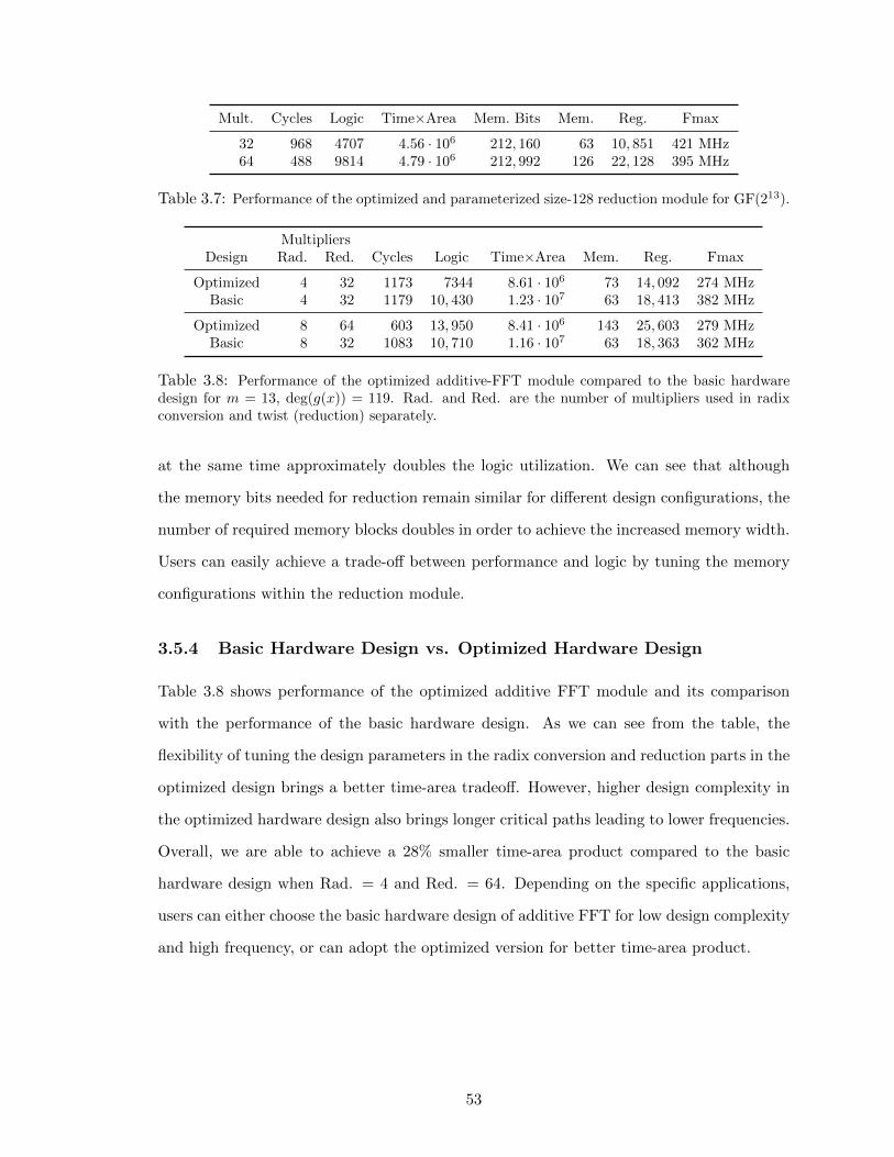
Mult. Cycles Logic Time×Area Mem. Bits Mem. Reg. Fmax
32 968 4707 4.56 · 106 212, 160 63 10, 851 421 MHz64 488 9814 4.79 · 106 212, 992 126 22, 128 395 MHz
Table 3.7: Performance of the optimized and parameterized size-128 reduction module for GF(213).
MultipliersDesign Rad. Red. Cycles Logic Time×Area Mem. Reg. Fmax
Optimized 4 32 1173 7344 8.61 · 106 73 14, 092 274 MHzBasic 4 32 1179 10, 430 1.23 · 107 63 18, 413 382 MHz
Optimized 8 64 603 13, 950 8.41 · 106 143 25, 603 279 MHzBasic 8 32 1083 10, 710 1.16 · 107 63 18, 363 362 MHz
Table 3.8: Performance of the optimized additive-FFT module compared to the basic hardwaredesign for m = 13, deg(g(x)) = 119. Rad. and Red. are the number of multipliers used in radixconversion and twist (reduction) separately.
at the same time approximately doubles the logic utilization. We can see that although
the memory bits needed for reduction remain similar for different design configurations, the
number of required memory blocks doubles in order to achieve the increased memory width.
Users can easily achieve a trade-off between performance and logic by tuning the memory
configurations within the reduction module.
3.5.4 Basic Hardware Design vs. Optimized Hardware Design
Table 3.8 shows performance of the optimized additive FFT module and its comparison
with the performance of the basic hardware design. As we can see from the table, the
flexibility of tuning the design parameters in the radix conversion and reduction parts in the
optimized design brings a better time-area tradeoff. However, higher design complexity in
the optimized hardware design also brings longer critical paths leading to lower frequencies.
Overall, we are able to achieve a 28% smaller time-area product compared to the basic
hardware design when Rad. = 4 and Red. = 64. Depending on the specific applications,
users can either choose the basic hardware design of additive FFT for low design complexity
and high frequency, or can adopt the optimized version for better time-area product.
53
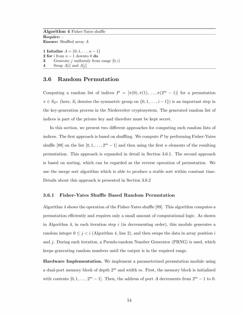
Algorithm 4 Fisher-Yates shuffle
Require: -Ensure: Shuffled array A
1 Initalize A = {0, 1, . . . , n− 1}2 for i from n− 1 downto 0 do3 Generate j uniformly from range [0, i)4 Swap A[i] and A[j]
3.6 Random Permutation
Computing a random list of indices P = [π(0), π(1), . . . , π(2m − 1)] for a permutation
π ∈ S2m (here, Si denotes the symmetric group on {0, 1, . . . , i− 1}) is an important step in
the key-generation process in the Niederreiter cryptosystem. The generated random list of
indices is part of the private key and therefore must be kept secret.
In this section, we present two different approaches for computing such random lists of
indices. The first approach is based on shuffling. We compute P by performing Fisher-Yates
shuffle [89] on the list [0, 1, . . . , 2m − 1] and then using the first n elements of the resulting
permutation. This approach is expanded in detail in Section 3.6.1. The second approach
is based on sorting, which can be regarded as the reverse operation of permutation. We
use the merge sort algorithm which is able to produce a stable sort within constant time.
Details about this approach is presented in Section 3.6.2
3.6.1 Fisher-Yates Shuffle Based Random Permutation
Algorithm 4 shows the operation of the Fisher-Yates shuffle [89]. This algorithm computes a
permutation efficiently and requires only a small amount of computational logic. As shown
in Algorithm 4, in each iteration step i (in decrementing order), this module generates a
random integer 0 ≤ j < i (Algorithm 4, line 2), and then swaps the data in array position i
and j. During each iteration, a Pseudo-random Number Generator (PRNG) is used, which
keeps generating random numbers until the output is in the required range.
Hardware Implementation. We implement a parameterized permutation module using
a dual-port memory block of depth 2m and width m. First, the memory block is initialized
with contents [0, 1, . . . , 2m − 1]. Then, the address of port A decrements from 2m − 1 to 0.
54

m Size (= 2m) Cycles (avg.) Logic Time×Area Mem. Reg. Fmax (MHz)
13 8192 23, 635 149 3.52 · 106 7 111 335
Table 3.9: Performance of the Fisher-Yates shuffle module for 213 elements.
For each address A, a PRNG keeps generating new random numbers as long as the output is
larger than address A. Therefore, our implementation produces a non-biased permutation
(under the condition that the PRNG has no bias) but it is not constant-time. Once the
PRNG output is smaller than address A, this output is used as the address for port B. Then
the contents of the cells addressed by A and B are swapped. We improve the probability of
finding a random index smaller than address A by using only dlog2(A)e bits of the PRNG
output. Therefore, the probability of finding a suitable B always is at least 50%.
Since we are using a dual-port memory in our implementation, the memory initialization
takes 2m−1 cycles. For the memory swapping operation, for each address A, first a valid
address B is generated and data stored in address A and B is read from the memory in
one clock cycle, then one more clock cycle is required for updating the memory contents.
On average, 2m−1 +∑m
i=1
∑2i−1−1j=0 ( 2i
2i−j + 1) cycles are needed for our Fisher-Yates shuffle
implementation. Table 3.9 shows performance data for the Fisher-Yates shuffle module.
3.6.2 Merge Sort Based Random Permutation
As we can easily see from Algorithm 4, different seeds for the PRNG will lead to different
cycle counts for the Fisher-Yates shuffle [89] based approach. This causes a potential risk
of timing side-channel attacks, which is hard to eliminate even if a larger PRNG is used.
To fully eliminate potential timing attacks using the Fisher-Yates shuffle approach,
in this section, we present a constant-time sorting module for permutation based on the
merge-sort algorithm. Sorting a random list can be regarded as the reverse operation
of a permutation: Sorting a randomly permuted list can be seen as applying swapping
operations on the elements until a sorted list is achieved. Applying the same swapping
operations in reverse order to a sorted list results in a randomly permuted list. Therefore,
given a constant-time sort algorithm, a constant-time algorithm for generating a random
permutation can easily be derived.
55

Algorithm 5 Merge sort algorithm.
Require: Random list A, of length 2k
Ensure: Sorted list A
1 Split A into 2k sublists.2 for i from 0 to k − 1 do3 Merge adjacent sublists.
Merge sort [90] is a comparison-based sorting algorithm which produces a stable sort, as
shown in Algorithm 5. For example, a given random list A = (92, 34, 18, 78, 91, 65, 80, 99)
can be sorted by using merge sort within three steps: Initially, list A is divided into eight
sublists (92), (34), (18), (78), (91), (65), (80), and (99) with granularity of one. Since there is
only one element in each sublist, these sublists are sorted. In the first step, all the adjacent
sublists are merged and sorted, into four sublists (34, 92), (18, 78), (65, 91), and (80, 99) of
size two. Merging of two sorted lists is simple: Iteratively, first elements of the lists are
compared and the smaller one is removed from its list and appended to the merged list,
until both lists are empty. In the second step, these lists are merged into two sublists
(18, 34, 78, 92) and (65, 80, 91, 99) of size four. Finally, these two sublists are merged to the
final sorted list Asorted = (18, 34, 65, 78, 80, 91, 92, 99).
In general, to sort a random list of n elements, merge sort needs log2(n) iterations, where
each step involves O(n) comparison-based merging operations. Therefore, merge sort has
an asymptotic complexity of O(n log2(n)).
Random Permutation. As mentioned above, sorting a random list can be regarded as
the reverse operation of permutation. When given a random list A, before the merge sort
process begins, we attach an index to each element in the list. Each element then has two
parts: value and index, where the value is used for comparison-based sorting, and the index
labels the original position of the element in list A. For the above example, to achieve a
permutation for list P = (0, 1, ..., 7), we first attach an index to each of the elements in A,
which gives us a new list A′ = ((92, 0), (34, 1), (18, 2), (78, 3), (91, 4), (65, 5), (80, 6), (99, 7)).
Then the merge sort process begins, which merges elements based on their value part, while
the index part remains unchanged. Finally, we get A′sorted = ((18, 2), (34, 1), (65, 5), (78, 3),
(80, 6), (91, 4), (92, 0), (99, 7)). By extracting the index part of the final result, we get a
56

random permutation of P , which is (2, 1, 5, 3, 6, 4, 0, 7). In general, to compute a random
permutation, we generate 2m random numbers and append each of them with an index.
The sorting result of these random numbers will uniquely determine the permutation.
In case there is a collision among the random values, the resulting permutation might
be slightly biased. Therefore, the bit-width of the randomly generated numbers needs to
be selected carefully to reduce the collision rate and thusly the bias. If the width of the
random numbers is b, then the probability that there are one or more collisions in 2m
randomly generated numbers is 1 −∏2m−1i=1
(2b−i)2b
due to the birthday paradox. Therefore,
for a given m, the collision rate can be reduced by using a larger b. However, increasing b
also increases the required logic and memory. Both m and b are parameters which can be
chosen at compile time in our implementation. The value for b can easily be chosen to fit
to the required m. For the parameters m = 13 and b = 32 the collision rate is 0.0078. We
further reduce the collision rate and thus the bias within merge sort by incorporating the
following trick in our design at low logic cost: In case the two random to-be-merged values
are equal, we do a conditional swap based on the least significant bit of the random value.
Since the least significant bit of the random value is random, this trick will make sure that
if some random numbers are generated twice, we can still get a non-biased permutation.
There still is going to be a bias in the permutation if some random values appear more
than two times. This case could be detected and the merge sort module could be restarted
repeatedly until no bias occurs. However, the probability of this is very low (prob ≈ 2−27.58
according to [91]) for m = 13 and b = 32.
Hardware Implementation. We implement a parameterized merge sort module using
two dual-port memory blocks P and P ′ of depth 2m and width (b + m). First, a PRNG
is used, which generates 2m random b-bit strings, each cell of memory block P then gets
initialized with one of the random b-bit strings concatenated with an m-bit index string
(corresponding to the memory address in this case). Once the initialization of P finishes,
the merge sort process starts. In our design, the merge sort algorithm is implemented in a
pipelined way. The basic three operations in the merge-sort module are: read values from
two sublists, compare the two values, and write down the smaller one to a new list. In our
57

Design Algorithm Const. Cycles Logic Time×Area Mem. Reg. Fmax
basic FY-shuffle × 23, 635 149 3.52 · 106 7 111 334 MHzOur merge-sort X 147, 505 448 6.61 · 107 46 615 365 MHz
Table 3.10: Performance of computing a permutation on 213 = 8192 elements with m = 13 andb = 32; Const. = Constant Time.
design, there are four pipeline stages: issue reads, fetch outputs from memory, compare the
outputs, and write back to the other memory. We build separate logic for these four stages
and time-multiplex these four stages by working on independent sublists in parallel whenever
possible. By having the four-stage pipelines, we achieve a high-performance merge-sort
design with a small logic overhead.
3.6.3 Fisher-Yates Shuffle vs. Merge Sort
Table 3.10 shows a comparison between the constant time, sort-based permutation module
with the non-constant time Fisher-Yates shuffle approach. Clearly, the constant-time per-
mutation implementation requires more time, area, and particularly memory. Therefore, a
trade-off needs to be made between the need for increased security due to the constant-time
implementation and resource utilization. In scenarios where timing side-channel protection
is not needed, the cheaper Fisher-Yates shuffle version might be sufficient.
3.7 Berlekamp-Massey Algorithm Based Decoding Unit
Finding a codeword at distance t from a vector v is the key step in the decryption operation.
We apply a decoding algorithm to solve this problem. Among different algorithms, the
Berlekamp-Massey (BM) algorithm [74] and Patterson’s algorithm [92] are the algorithms
most commonly used. Patterson’s algorithm takes advantage of certain properties present
in binary Goppa codes, and is able to correct up to t errors for binary Goppa codes with a
designated minimum distance dmin ≥ 2t+1. On the other hand, general decoding algorithms
like the BM algorithm can only correct t2 errors by default, which can be increased to t errors
using the trick proposed by Nicolas Sendrier [65]. However, the process of BM algorithm is
quite simple compared to Patterson’s algorithm. More importantly, it is easier to protect
58

entry_sum(Vector mult.)
Ϭ(x) = 1
β(x) = 1
l = 0
k = 0
δ-1
β'(x)
Ϭ'(x)
t, S(x)
GF(2m) inv.
δ = 0
d
GF(2m) mult.δ-1
dδ-1
Scalar mult.β(x)
dδ-1β(x) Vector add.
Ϭ(x)
Binary shiftIf condition
(d = 0 or k < 2l)
Add/Sub.
k' = k + 1
k
l
k
l'
k'
δ' = d or δ
δ-1
δ'
δ
Berlekamp-Massey Step
d
Figure 3.6: Dataflow diagram of the Berlekamp-Massey module.
the implementation of BM algorithm against timing attacks given the simplicity of the
decryption steps. Consequently, we use BM algorithm in our decryption module.
Our implementation follows the Berlekamp iterative algorithm as described in [74].
The algorithm begins with initializing polynomials σ(x) = 1 ∈ GF(2m)[x], β(x) = x ∈
GF(2m)[x], integers l = 0 and δ = 1 ∈ GF(2m). The input syndrome polynomial is denoted
as S(x) =∑2t−1
i=1 Sixi ∈ GF(2m)[x]. Then within each iteration step k (0 ≤ k ≤ 2t − 1),
the variables {σ(x), β(x), l, δ} are conditionally updated using operations described in Al-
gorithm 6. Note that updating polynomial β(x) only involves multiplying a polynomial by
x, which can be easily mapped to a binary shifting operation on its coefficients in hardware.
Similarly, the updates of integer l and field element δ only involve cheap operations includ-
ing subtraction and addition. These operations can be easily implemented in hardware as
well. Therefore the bottleneck of the algorithm lies in computing d and updating σ(x).
Hardware Implementation. The first step within each iteration is to calculate d (Alg. 6,
line 3). We built an entry sum module (as shown in Figure 3.6) for this computation, which
maps to a vector-multiplication operation. We use two registers σvec and βvec of m · (t+ 1)
59

Algorithm 6 Berlekamp-Massey algorithm for decryption.
Require: Public security parameter t, syndrome polynomial S(x).Ensure: Error locator polynomial σ(x).
1 Initialize: σ(x) = 1, β(x) = x, l = 0, δ = 1.2 for k from 0 to 2t− 1 do3 d =
∑ti=0 σiSk−i
4 if d = 0 or k < 2l:5 {σ(x), β(x), l, δ} =
{σ(x)− dδ−1β(x), xβ(x), l, δ
}.
6 else:7 {σ(x), β(x), l, δ} =
{σ(x)− dδ−1β(x), xσ(x), k − l + 1, d
}.
8 Return the error locator polynomial σ(x).
bits to store the coefficients of polynomials σ(x) and β(x), where the constant terms σ0 and
β0 are stored in the lowest m bits of the registers, σ1 and β1 are stored in the second lowest
m bits, and so on. We also use a register Svec of m ·(t+1) bits to store at most (t+1) coeffi-
cients of S(x). This register is updated within each iteration, where Sk is stored in the least
significant m bits of the register, Sk−1 is stored in the second least significant m bits, and
so on. The computation of d can then be regarded as an entry-wise vector multiplication
between register σvec and register Svec = (0, 0, ..., S0, S1, ..., Sk−1, Sk) for all 0 ≤ k ≤ 2t− 1.
Register σvec is initialized as (0, 0, ..., 1) for the first iteration, and then gets updated with
the new coefficients of σ(x) for the next iteration. Svec is initialized as all zeroes, and then
constructed gradually by reading from a piece of memory which stores coefficient Si of syn-
drome polynomial S(x) at address i for 0 ≤ i ≤ 2t − 1. Within the k-th iteration, a read
request for address k of the memory is issued. Once the corresponding coefficient Sk is read
out, it is inserted to the lowest m bits of Svec. After the computation of d, we start updating
variables {σ(x), β(x), l, δ}. To update σ(x), one field-element inversion, one field-element
multiplication, one scalar multiplication as well as one vector subtraction are needed. At
first, field element δ is inverted. As described in Section 3.3, the inversion of elements in
GF(2m) can be implemented by use of a pre-computed lookup table. Each entry of the table
can be read in one clock cycle. After reading out δ−1, a field-element multiplication between
d and δ−1 is performed, which makes use of the GF(2m) multiplication module as described
in Section 3.3. Once we get dδ−1, a scalar multiplication between field element dδ−1 and
polynomial β(x) starts, which can be mapped to an entry-wise vector multiplication be-
tween vector (dδ−1, dδ−1, ..., dδ−1) and (βt, βt−1, ..., β1, β0). The last step for updating σ(x)
60

mulBM mulBM step Cycles Logic Time×Area Mem. Reg. Fmax
10 10 7379 6285 4.64 · 107 7 13, 089 364 MHz20 20 4523 7052 3.19 · 107 7 13, 031 353 MHz30 30 3571 7889 2.82 · 107 7 12, 956 361 MHz40 40 3095 9047 2.8 · 107 7 13, 079 356 MHz60 60 2619 11, 400 2.99 · 107 7 13, 274 354 MHz
Table 3.11: Performance of the Berlekamp-Massey module for security parameters m = 13, t = 119,and deg(S(x)) = 237.
is to subtract dδ−1β(x) from σ(x). In a binary field GF(2m), subtraction and addition
operations are equivalent. Therefore, the subtraction between σ(x) and dδ−1β(x) can sim-
ply be mapped to bit-wise xor operations between vector (σt, σt−1, ..., σ1, σ0) and vector
(dδ−1βt, dδ−1βt−1, ..., dδ
−1β1, dδ−1β0). Updating polynomial β(x) is done by conditionally
replacing its coefficient register βvec with δvec, and then shift the resulting value leftwards
by m bits. Similarly, the updates of integer l and field element δ only involve simple and
cheap hardware operations.
The above iterations are repeated for a fixed number of 2t times, where t is the public
security parameter. After 2t iterations, the final output is determined as the error locator
polynomial σ(x). It is easy to see that within each iteration, the sequence of instructions is
fixed, as long as we make sure that the conditional updates of variables {σ(x), β(x), l, δ} are
constant time (which is easy to achieve due to its fixed computational mapping in hardware),
the run time of the whole design is fixed given the fixed iteration times. Therefore our BM
implementation is fully protected against existing timing side-channel attacks, e.g., [93,94].
We build a two-level design. The lower level is a BM step module, which maps to one
iteration, shown as “Berlekamp-Massey Step” in Figure 3.6. The higher-level BM module
then iteratively applies BM step and entry sum modules.
Performance Evaluation. Table 3.11 shows performance for the BM module. A time-
area trade-off can be achieved by adjusting the design parameters mulBM and mulBM step,
which are the number of multipliers used in the BM and BM step modules. mulBM and
mulBM step can be freely chosen as integers between 1 and t+ 1.
61

3.8 Full Niederreiter Cryptosystem on Hardware
H
R RGenerator
PRNG
GF(2m)Gaussian
Systemizer
g-portion
g(x)Evaluation(Additive FFT)
HGenerator
g_out
PGenerator(FYS or Sort)
P
P_out
GF(2)Gaussian
Systemizer
K_out
PRNG
Permutation Gen.
Goppa Polynomial Gen.
Public Key K Gen.
K-portionC
D
P'
I
I
M
(a) Key generation
(b) Encryption
g(x)Evaluation(Additive FFT)
C
DDoubled
Syndrome
SK_g(x)
SK_P
Berlekamp Massey
ErrorLocator
Ciphertext Recovered Message
I IM
(c) Decryption
Figure 3.7: Dataflow diagrams of the three parts of the cryptosystem: (a) key generation, (b)encryption, and (c) decryption. Dark gray boxes represent block memories, while white boxesrepresent major logic modules.
We design the Niederreiter cryptosystem by using the main building blocks shown in
Figure 3.7. Note that we are using two simple 64-bit Xorshift PRNGs in our design to
enable deterministic testing. For real deployment, these PRNGs must be replaced with a
cryptographically secure random-number generator, e.g., [95]. We require at most b random
bits per clock cycle per PRNG.
62
3.8.1 Key Generator Module
Using two Gaussian systemizers, Gao-Mateer additive FFT, and the permutation unit, we
present two similar key generators as shown in Figure 3.7a. The overall design of these two
key-generation modules are mostly identical except that the basic key generator is based on
the Fisher-Yates shuffling module and the basic hardware design of additive FFT while the
optimized key generator is based on the Merge-Sort module and the optimized hardware
design of additive FFT.
3.8.1.1 Secret Key Generation
The private key consists of an irreducible Goppa polynomial g(x) of degree t and a permuted
list of indices P .
Goppa Polynomial g(x). The common way for generating a degree-d irreducible polyno-
mial is to pick a polynomial g of degree d uniformly at random, and then to check whether
it is irreducible or not. If it is not, a new polynomial is randomly generated and checked,
until an irreducible one is found. The density of irreducible polynomials of degree d is
about 1/d [32]. When d = t = 119, the probability that a randomly generated degree-119
polynomial is irreducible gets quite low. On average, 119 trials are needed to generate a
degree-119 irreducible polynomial in this way. Moreover, irreducibility tests for polynomials
involve highly complex operations in extension fields, e.g., raising a polynomial to a power
and finding the greatest common divisor of two polynomials. In the hardware key generator
design in [67], the Goppa polynomial g(x) was generated in this way, which is inefficient in
terms of both time and area.
We decide to explicitly generate an irreducible polynomial g(x) by using a deterministic,
constructive approach. We compute the minimal (hence irreducible) polynomial of a random
element in GF(2m)[x]/h with deg(h) = deg(g) = t: Given a random element r from the
extension field GF(2m)[x]/h, the minimal polynomial g(x) of r is defined as the non-zero
monic polynomial of least degree with coefficients in GF(2m) having r as a root, i.e., g(r) =
0. The minimal polynomial of a degree-(t− 1) element from field GF(2m)[x]/h is always of
degree t and irreducible if it exists.
63

The process of generating the minimal polynomial g(x) = g0 + g1x+ · · ·+ gt−1xt−1 + xt
of a random element r(x) =∑t−1
i=0 rixi is as follows: Since g(r) = 0, we have g0 + g1r+ · · ·+
gt−1rt−1+rt = 0 which can be equivalently written using vectors as: (1T , rT , . . . , (rt−1)T , (rt)T )·
(g0, g1, . . . , gt−1, 1)T = 0. Note that since R = (1T , rT , . . . , (rt−1)T , (rt)T ) is a t × (t + 1)
matrix while g = (g0, g1, . . . , gt−1, 1)T is a size-(t+ 1) vector, we get
R · g =
0 rt−1 · · · (rt)t−1
0 rt−2 · · · (rt)t−2...
.... . .
...
0 r1 · · · (rt)1
1 r0 · · · (rt)0
g0
g1...
gt−1
1
= 0.
Now, we can find the minimal polynomial of r by treating g as variable and by solving
the resulting system of linear equations for g. By expanding this matrix-vector multi-
plication equation, we get t linear equations which uniquely determine the solution for
(g0, g1, . . . , gt−1). Solving systems of linear equations can be easily transformed into a ma-
trix systemization problem, which can be handled by performing Gaussian elimination on
the coefficient matrix R.
In our hardware implementation, first a PRNG is used, which generates t random m-bit
strings for the coefficients of r(x) =∑t−1
i=0 rixi. Then the coefficient matrix R is calculated
by computing the powers of 1, r, . . . , rt, which are stored in the memory of the GF(2m)
Gaussian systemizer. We repeatedly use the polynomial multiplier described in Section
3.3.2 to compute the powers of r. After each multiplication, the resulting polynomial of t
coefficients is written to the memory of the GF(2m) Gaussian systemizer. (Our Gaussian-
systemizer module operates on column-blocks of width NR. Therefore, the memory contents
are actually computed block-wise.) This multiply-then-write-to-memory cycle is repeated
until R is fully calculated. After this step is done, the memory of the GF(2m) Gaussian
systemizer has been initialized with the coefficient matrix R.
After the initialization, the Gaussian elimination process begins and the coefficient ma-
trix R is transformed into its reduced echelon form [It|g]. Now, the right part of the resulting
64
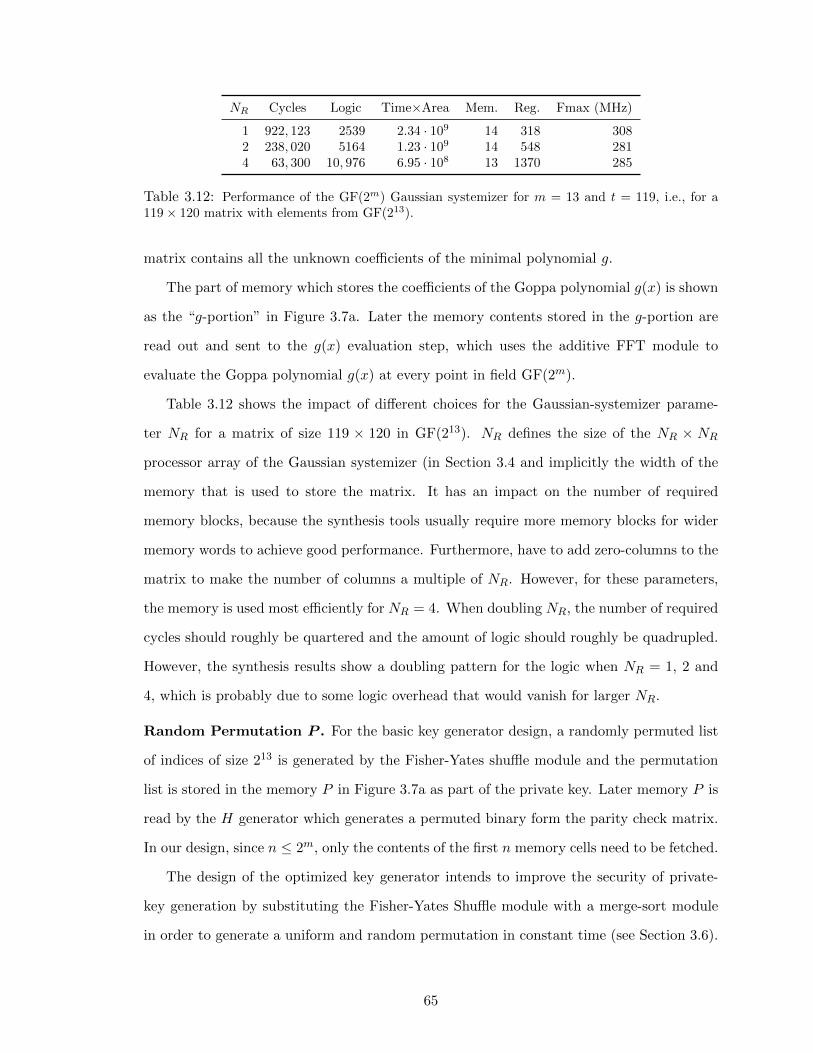
NR Cycles Logic Time×Area Mem. Reg. Fmax (MHz)
1 922, 123 2539 2.34 · 109 14 318 3082 238, 020 5164 1.23 · 109 14 548 2814 63, 300 10, 976 6.95 · 108 13 1370 285
Table 3.12: Performance of the GF(2m) Gaussian systemizer for m = 13 and t = 119, i.e., for a119× 120 matrix with elements from GF(213).
matrix contains all the unknown coefficients of the minimal polynomial g.
The part of memory which stores the coefficients of the Goppa polynomial g(x) is shown
as the “g-portion” in Figure 3.7a. Later the memory contents stored in the g-portion are
read out and sent to the g(x) evaluation step, which uses the additive FFT module to
evaluate the Goppa polynomial g(x) at every point in field GF(2m).
Table 3.12 shows the impact of different choices for the Gaussian-systemizer parame-
ter NR for a matrix of size 119 × 120 in GF(213). NR defines the size of the NR × NR
processor array of the Gaussian systemizer (in Section 3.4 and implicitly the width of the
memory that is used to store the matrix. It has an impact on the number of required
memory blocks, because the synthesis tools usually require more memory blocks for wider
memory words to achieve good performance. Furthermore, have to add zero-columns to the
matrix to make the number of columns a multiple of NR. However, for these parameters,
the memory is used most efficiently for NR = 4. When doubling NR, the number of required
cycles should roughly be quartered and the amount of logic should roughly be quadrupled.
However, the synthesis results show a doubling pattern for the logic when NR = 1, 2 and
4, which is probably due to some logic overhead that would vanish for larger NR.
Random Permutation P . For the basic key generator design, a randomly permuted list
of indices of size 213 is generated by the Fisher-Yates shuffle module and the permutation
list is stored in the memory P in Figure 3.7a as part of the private key. Later memory P is
read by the H generator which generates a permuted binary form the parity check matrix.
In our design, since n ≤ 2m, only the contents of the first n memory cells need to be fetched.
The design of the optimized key generator intends to improve the security of private-
key generation by substituting the Fisher-Yates Shuffle module with a merge-sort module
in order to generate a uniform and random permutation in constant time (see Section 3.6).
65

3.8.1.2 Public Key Generation
As described in Section 3.2, the public key K is the systemized form of the binary version of
the parity check matrix H. In [67], the generation of the binary version of H is divided into
two steps: first compute the non-permuted parity check matrix and store it in a memory
block A, then apply the permutation and write the binary form of the permuted parity-
check matrix to a new memory block B, which is of the same size as memory block A. This
approach requires simple logic but needs two large memory blocks A and B.
In order to achieve better memory efficiency, we omit the first step, and instead generate
a permuted binary form H ′ of the parity check matrix in one step. We start the generation
of the public key K by evaluating the Goppa polynomial g(x) at all α ∈ GF(2m) using the
Gao-Mateer additive FFT module. After the evaluation finishes, the results are stored in
the data memory of the additive FFT module.
Now, we generate the permuted binary parity check matrixH ′ and store it in the memory
of the GF(2) Gaussian systemizer. Suppose the permutation indices stored in memory P
are [p0, p1, . . . , pn−1, . . . , p2m−1], then
H ′ =
1/g(αp0) 1/g(αp1) · · · 1/g(αpn−1)
αp0/g(αp0) αp1/g(αp1) · · · αpn−1/g(αpn−1)
......
. . ....
αt−1p0 /g(αp0) αt−1p1 /g(αp1) · · · αt−1pn−1/g(αpn−1)
.
To generate the first column of H ′, the first element p0 from P is fetched and stored in
a register. Then, the corresponding polynomial evaluation value g(αp0) is read out from
the data memory of the additive FFT module. This value is then inverted using a GF(2m)
inverter. After inversion, we get 1/g(αp0) which is the first entry of the column. The second
entry is calculated by a multiplication of the first entry row and αp0 , the third entry again is
calculated by a multiplication of the previous row and αp0 and so on. Each time a new entry
is generated, it is written to the memory of the GF(2) Gaussian systemizer (bit-wise, one
bit per row). This computation pattern is repeated for all p0, p1, . . . , pn−1 until H ′ is fully
calculated. After this step, the memory of the GF(2) Gaussian systemizer contains H ′ and
66
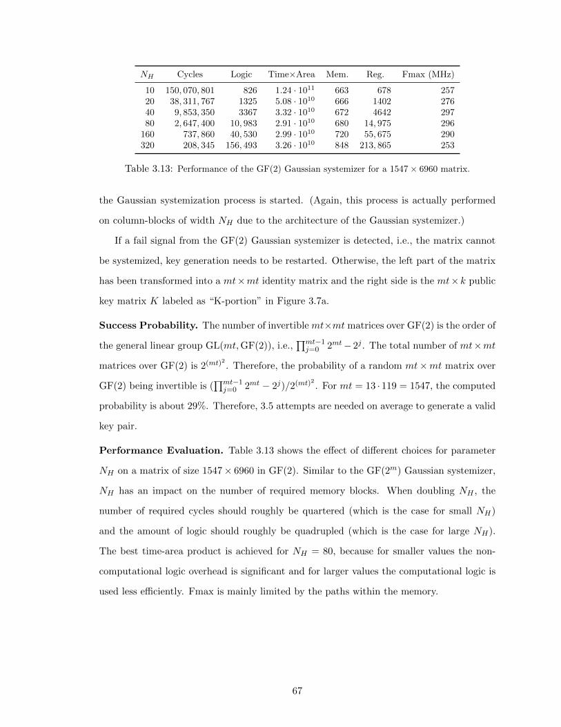
NH Cycles Logic Time×Area Mem. Reg. Fmax (MHz)
10 150, 070, 801 826 1.24 · 1011 663 678 25720 38, 311, 767 1325 5.08 · 1010 666 1402 27640 9, 853, 350 3367 3.32 · 1010 672 4642 29780 2, 647, 400 10, 983 2.91 · 1010 680 14, 975 296
160 737, 860 40, 530 2.99 · 1010 720 55, 675 290320 208, 345 156, 493 3.26 · 1010 848 213, 865 253
Table 3.13: Performance of the GF(2) Gaussian systemizer for a 1547× 6960 matrix.
the Gaussian systemization process is started. (Again, this process is actually performed
on column-blocks of width NH due to the architecture of the Gaussian systemizer.)
If a fail signal from the GF(2) Gaussian systemizer is detected, i.e., the matrix cannot
be systemized, key generation needs to be restarted. Otherwise, the left part of the matrix
has been transformed into a mt×mt identity matrix and the right side is the mt×k public
key matrix K labeled as “K-portion” in Figure 3.7a.
Success Probability. The number of invertible mt×mt matrices over GF(2) is the order of
the general linear group GL(mt,GF(2)), i.e.,∏mt−1j=0 2mt−2j . The total number of mt×mt
matrices over GF(2) is 2(mt)2. Therefore, the probability of a random mt×mt matrix over
GF(2) being invertible is (∏mt−1j=0 2mt − 2j)/2(mt)
2. For mt = 13 · 119 = 1547, the computed
probability is about 29%. Therefore, 3.5 attempts are needed on average to generate a valid
key pair.
Performance Evaluation. Table 3.13 shows the effect of different choices for parameter
NH on a matrix of size 1547× 6960 in GF(2). Similar to the GF(2m) Gaussian systemizer,
NH has an impact on the number of required memory blocks. When doubling NH , the
number of required cycles should roughly be quartered (which is the case for small NH)
and the amount of logic should roughly be quadrupled (which is the case for large NH).
The best time-area product is achieved for NH = 80, because for smaller values the non-
computational logic overhead is significant and for larger values the computational logic is
used less efficiently. Fmax is mainly limited by the paths within the memory.
67

Case NH NR Cycles Logic Time×Area Mem. Fmax Time
Basic Hardware Implementationlogic 40 1 11, 121, 220 29, 711 3.30 · 1011 756 240 MHz 46.43 msbal. 80 2 3, 062, 942 48, 354 1.48 · 1011 764 248 MHz 12.37 mstime 160 4 896, 052 101, 508 9.10 · 1010 803 244 MHz 3.68 ms
Optimized Hardware Implementationlogic 40 1 11, 121, 214 22, 716 2.53 · 1011 819 237 MHz 46.83 msbal. 80 2 3, 062, 936 39, 122 1.20 · 1011 827 230 MHz 13.34 mstime. 160 4 966, 400 88, 715 8.57 · 1010 873 251 MHz 3.85 ms
Table 3.14: Performance of the key-generation module for parameters m = 13, t = 119, andn = 6960. All the numbers in the table come from compilation reports of the Altera tool chain forStratix V FPGAs.
3.8.1.3 Basic vs. Optimized Key Generators
Table 3.14 shows a comparison of the performance of the basic implementation with the
optimized implementation of the key generator. As we can see from the table, these two
designs achieve similar cycles counts and time for the key generation operation. For the
optimized key generator design, despite the higher cost for the constant-time permutation
module, overall, it achieves an improvement in regard to area requirements and therefore
to the time-area product at roughly the same frequency on the price of a higher memory
demand. However, the overall memory increase is less than 10% can be justified by the
increased side-channel resistance due to the use of a constant-time permutation. Depending
on the specific application and resource budgets, users can choose from one of the designs.
3.8.2 Encryption Module
Figure 3.7b shows the interface of the encryption module. The encryption module as-
sumes that the public key K is fed in column by column. The matrix-vector multiplication
[Imt|K] × e is mapped to serial xor operations. Once the PK column valid signal is high,
indicating that a new public-key column (PK column) is available at the input port, the
module checks if the corresponding bit of plaintext e is 1 or 0. If the bit value is 1, then
an xor operation between the current output register (initialized as 0) and the new public-
key column is carried out. Otherwise, no operation is performed. After the xor operation
between K and the last (n−mt) bits of e is finished, we carry out one more xor operation
68
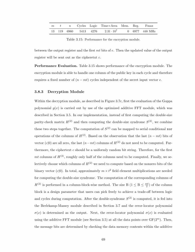
m t n Cycles Logic Time×Area Mem. Reg. Fmax
13 119 6960 5413 4276 2.31 · 107 0 6977 448 MHz
Table 3.15: Performance for the encryption module.
between the output register and the first mt bits of e. Then the updated value of the output
register will be sent out as the cipheretxt c.
Performance Evaluation. Table 3.15 shows performance of the encryption module. The
encryption module is able to handle one column of the public key in each cycle and therefore
requires a fixed number of (n−mt) cycles independent of the secret input vector e.
3.8.3 Decryption Module
Within the decryption module, as described in Figure 3.7c, first the evaluation of the Goppa
polynomial g(x) is carried out by use of the optimized additive FFT module, which was
described in Section 3.5. In our implementation, instead of first computing the double-size
parity-check matrix H(2) and then computing the double-size syndrome S(2), we combine
these two steps together. The computation of S(2) can be mapped to serial conditional xor
operations of the columns of H(2). Based on the observation that the last (n−mt) bits of
vector (c|0) are all zero, the last (n−mt) columns of H(2) do not need to be computed. Fur-
thermore, the ciphertext c should be a uniformly random bit string. Therefore, for the first
mt columns of H(2), roughly only half of the columns need to be computed. Finally, we se-
lectively choose which columns of H(2) we need to compute based on the nonzero bits of the
binary vector (c|0). In total, approximately m× t2 field element multiplications are needed
for computing the double-size syndrome. The computation of the corresponding columns of
H(2) is performed in a column-block-wise method. The size B (1 ≤ B ≤ mt2 ) of the column
block is a design parameter that users can pick freely to achieve a trade-off between logic
and cycles during computation. After the double-syndrome S(2) is computed, it is fed into
the Berlekamp-Massey module described in Section 3.7 and the error-locator polynomial
σ(x) is determined as the output. Next, the error-locator polynomial σ(x) is evaluated
using the additive FFT module (see Section 3.5) at all the data points over GF(2m). Then,
the message bits are determined by checking the data memory contents within the additive
69
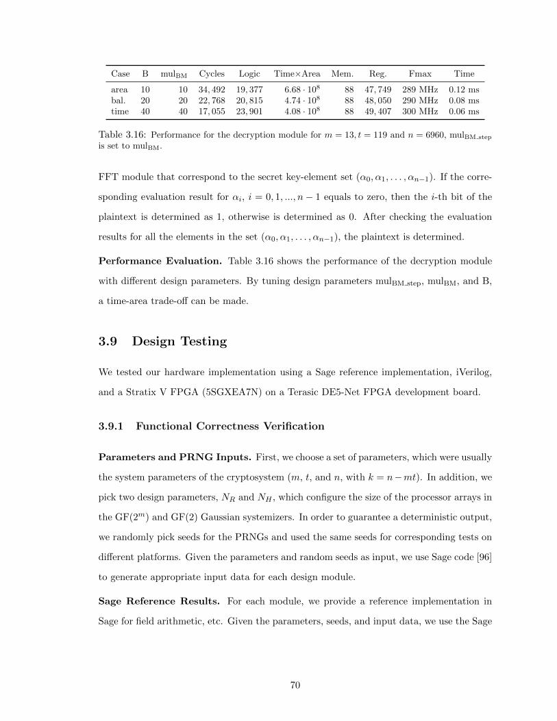
Case B mulBM Cycles Logic Time×Area Mem. Reg. Fmax Time
area 10 10 34, 492 19, 377 6.68 · 108 88 47, 749 289 MHz 0.12 msbal. 20 20 22, 768 20, 815 4.74 · 108 88 48, 050 290 MHz 0.08 mstime 40 40 17, 055 23, 901 4.08 · 108 88 49, 407 300 MHz 0.06 ms
Table 3.16: Performance for the decryption module for m = 13, t = 119 and n = 6960, mulBM step
is set to mulBM.
FFT module that correspond to the secret key-element set (α0, α1, . . . , αn−1). If the corre-
sponding evaluation result for αi, i = 0, 1, ..., n− 1 equals to zero, then the i-th bit of the
plaintext is determined as 1, otherwise is determined as 0. After checking the evaluation
results for all the elements in the set (α0, α1, . . . , αn−1), the plaintext is determined.
Performance Evaluation. Table 3.16 shows the performance of the decryption module
with different design parameters. By tuning design parameters mulBM step, mulBM, and B,
a time-area trade-off can be made.
3.9 Design Testing
We tested our hardware implementation using a Sage reference implementation, iVerilog,
and a Stratix V FPGA (5SGXEA7N) on a Terasic DE5-Net FPGA development board.
3.9.1 Functional Correctness Verification
Parameters and PRNG Inputs. First, we choose a set of parameters, which were usually
the system parameters of the cryptosystem (m, t, and n, with k = n−mt). In addition, we
pick two design parameters, NR and NH , which configure the size of the processor arrays in
the GF(2m) and GF(2) Gaussian systemizers. In order to guarantee a deterministic output,
we randomly pick seeds for the PRNGs and used the same seeds for corresponding tests on
different platforms. Given the parameters and random seeds as input, we use Sage code [96]
to generate appropriate input data for each design module.
Sage Reference Results. For each module, we provide a reference implementation in
Sage for field arithmetic, etc. Given the parameters, seeds, and input data, we use the Sage
70

reference implementation to generate reference results for each module.
iVerilog Simulation Results. We simulate the Verilog HDL code of each module using
a “testbench” top module and the iVerilog simulator [97]. At the end of the simulation, we
store the simulation result in a file. Finally, we compare the simulation result with the Sage
reference result. If these reference and simulation results matched repeatedly for different
inputs, we assume the Verilog HDL code to be correct.
3.9.2 FPGA Evaluation Platform
We evaluated our design on an Intel (formerly Altera) Stratix V FPGA (5SGXEA7N) on
a Terasic DE5-Net FPGA development board. This device has about 234,720 adaptive
logic modules (ALMs) and about 2,560 M20K blocks, which is the basic on-chip memory
resource unit available in Stratix V families. Each M20K is a synchronous, true dual-port
memory block, with 20,480 programmable bits. We used Intel Quartus Software Version
17.0 (Standard Edition) for synthesis.
3.9.3 Hardware Prototype Setup
To validate the FPGA implementation, in addition to simulations, we implement a serial IO
interface for communication between the host computer and the FPGA. A diagram showing
the complete testing setup is provided in Figure 3.8. The interface allows us to send data
and simple commands from the host to the FPGA and receive data, e.g., public and private
key, ciphertext, and plaintext, from the FPGA. We verified the correct operation of our
design by comparing the FPGA outputs with our Sage reference implementation (using the
same PRNG and random seeds).
3.10 Performance Evaluation
As explained in Section 3.2.4, our implementation of the Niederreiter cryptosystem is fully
parameterized and can be synthesized for any choice of reasonable security parameters.
However, the main target of our implementation is the 256-bit (classical) security level,
which corresponds to a level at least “128-bit post-quantum security”. For testing, we
71

Real-time Display
Send Commands&Data
Returned Results
Verification
CPU
DISPLAY FPGA POWER SUPPLY
RS422 CABLE
USB
FPGA Chip
workstation(verification of results) State
Machine
UART
KeyGeneration
Encryption
Decryption
Figure 3.8: Diagram of the hardware prototype setup, including the FPGA, a host computer, anda display.
use the parameters suggested in the PQCRYPTO recommendations [76] and the “Classic
McEliece” third round submission: m = 13, t = 119, n = 6960 and k = 5413 (k = n−mt).
The results are given in Table 3.17, with included logic overhead of the input and output
(IO) interface. We provide numbers for three performance parameter sets, one for small
area, one for small runtime, and one for balanced time and area. The parameters NR and
NH control the size of the systolic array in the Gaussian systemizer modules, which are
used for computing the private Goppa polynomial and the public key. Parameter B is
the matrix-block size used for computing the syndrome. Parameter mulBM determines the
number of multipliers used in the high-level BM decoding module. The number of multipliers
(mulBM step) used in the low-level BM step module is set to mulBM for the evaluation. The
memory requirement varies slightly due the differences in the memory word size based on the
design parameters. These design parameters can be freely chosen as long as the synthesized
result fits on the target FPGA. For security parameter set m = 13, t = 119, n = 6960, our
experiment shows that the largest design parameter set we can fit on Stratix V FPGA is:
NR = 250, NH = 6, mulBM = 60, mulBM step = 60, and B = 60.
72

Case NH NR B mulBM Logic Mem. Reg. Fmax
area 40 1 10 10 53, 447 (23%) 907 (35%) 118, 243 245 MHzbal. 80 2 20 20 70, 478 (30%) 915 (36%) 146, 648 251 MHztime 160 4 40 40 121, 806 (52%) 961 (38%) 223, 232 248 MHz
Table 3.17: Performance for the entire Niederreiter cryptosystem (i.e., key generation, encryption,and decryption) including the serial IO interface when synthesized for the Stratix V (5SGXEA7N)FPGA; mulBM step is set to mulBM.
Cycles Logic Freq. Mem. Time (ms)Gen. Dec. Enc. (MHz) Gen. Dec. Enc.
m = 11, t = 50, n = 2048, Virtex 5 LX110[67] 14, 670, 000 210, 300 81, 500 14, 537 163 75 90.00 1.29 0.50
Oura 1, 503, 927 5864 1498 6660 180 68 8.35 0.03 0.01
m = 12, t = 66, n = 3307, Virtex 6 LX240[66] — 28, 887 — 3307 162 15 — 0.18 —
Ourb — 10, 228 — 6571 267 23 — 0.04 —Ourc 4, 929, 400 10, 228 2515 17, 331 160 142 30.00 0.06 0.02
m = 13, t = 128, n = 8192, Haswell vs. StratixV[98] 1, 236, 054, 840 343, 344 289, 152 — 4000 — 309.01 0.09 0.07
Ourd 1, 173, 750 17, 140 6528 129, 059 231 1126 5.08 0.07 0.03
a (NH, NR, B, mulBM, mulBM step) = (20, 2, 20, 20, 20), entire Niederreiter cryptosystem.b (B, mulBM, mulBM step) = (20, 20, 20), decryption module.c (NH, NR, B, mulBM, mulBM step) = (20, 2, 20, 20, 20), entire Niederreiter cryptosystem.d (NH, NR, B, mulBM, mulBM step) = (160, 4, 80, 65, 65), entire Niederreiter cryptosystem.
Table 3.18: Comparison with related work. Logic is given in “Slices” for Xilinx Virtex FPGAs andin “ALMs” for Altera Stratix FPGAs.
3.11 Comparison with Related Work
First, we compare it with a 103-bit classical security-level hardware-design described in [67].
This work is the only previously existing hardware implementation for the whole code-based
cryptosystem, including a key generator, that we have found in literature. To compare with
their work, we synthesized our design with the Xilinx tool-chain version 14.7 for a Virtex-
5 XC5VLX110 FPGA. Note that the performance data of [67] in Table 3.18 includes a
CCA2 conversion for encryption and decryption, which adds some overhead compared to
our design. From Table 3.18, we can see that our design is much faster when comparing
cycles and time, and also much cheaper in regard to area and memory consumption.
Second, we compare our work with a hardware design from [66], which presents the pre-
viously fastest decryption module for a McEliece cryptosystem. Therefore the comparison
73

of our work with design [66] focuses on the decryption part. We synthesized our decryption
module with the parameters they used, which correspond to a 128-bit classical security
level, for a Virtex-6 XC6VLX240T FPGA. From Table 3.18, we can see that the time-area
product of our decryption module is 10228 · 6571 = 67, 208, 188, which is 30% smaller than
the time-area product of their design of 28887 ·3307 = 95, 529, 309 when comparing only the
decryption module. Moreover, our design is able to achieve a much higher frequency and a
smaller cycle counts compared to their design. Overall we are more than 4x faster than [66].
Apart from this, we also provide the performance of the entire Niederreiter cryptosystem
corresponding to security parameter set m = 12, t = 66, n = 3307 when synthesized for a
Virtex 6 XC6VLX240T FPGA.
Finally, we also compare the performance of our hardware design with the to-date fastest
CPU implementation of the Niederreiter cryptosystem [98]. In this case, we ran our im-
plementation on our Altera Stratix V FPGA and compare it to a Haswell CPU running at
4 GHz. Our implementation competes very well with the CPU implementation, despite the
over 10x slower clock of the FPGA.
3.12 Chapter Summary
In this chapter, we presented a complete hardware implementation of Niederreiter’s code-
based cryptosystem based on binary Goppa codes. Our hardware design of the complex
code-based Niederreiter cryptosystem is the first work that presents architectures for all the
key operations in the cryptosystem, including the most expensive key generator unit. The
presented design can be configured with tunable security parameter sets, as well as different
performance parameters targeting different applications. By designing novel and efficient
hardware accelerators, we successfully demonstrate the feasibility of running complex code-
based cryptosystems on hardware. our hardware design of the Niederreiter cryptosystem
can serve as an efficient and ready-to-deploy solution for many high-end applications, e.g.,
cloud servers.
74
Chapter 4
Hash-based Cryptography:
Software-Hardware Co-Design of
XMSS
While the pure hardware design for the Niederreiter cryptosystem serves as a ready-to-
use candidate for many high-end applications (e.g., cloud servers), PQC-based solutions
are also needed for low-end embedded devices. Embedded devices such as smart cards
and portable medical devices play an important role in our daily life. Despite their typi-
cally constrained resources, these devices require strong security measures to protect them
against cyber attacks. How to run PQC algorithms, which have relatively high resource
requirements, efficiently without incurring large logic and memory overhead on these em-
bedded devices is an open research question. This chapter tackles this research problem by
adopting a heterogenous software-hardware co-design approach combining the flexibility of
a soft processor with the acceleration from the dedicated hardware accelerators. Especially,
we present a software-hardware co-design based on an open-source RISC-V platform for the
stateful hash-based signature scheme XMSS on the FPGA platform, which has been stan-
dardized by IETF in 2018 and more recently was recommended by NIST for early use [6]
as a post-quantum secure digital signature scheme. The experimental results show a signif-
icant speedup of running XMSS on our software-hardware co-design compared to the pure
75
reference software version, and have successfully demonstrated the feasibility and efficiency
of deploying XMSS for embedded applications.
4.1 Background
Due to the continued computerization and automation of our society, more and more sys-
tems from consumer products and Internet-of-Things (IoT) devices to cars, high-speed
trains, and even nuclear power plants are controlled by embedded computers that often are
connected to the Internet. Such devices can have a severe impact not only on our informa-
tion security but increasingly also on our physical safety. Therefore, embedded devices must
provide a high level of protection against cyber attacks – despite their typically restricted
computing resources. If an attacker is able to disrupt the authenticity of transmitted data,
he or she can undermine the security of the system in many ways, e.g., malicious firmware
can be loaded or contents of a digital document can be changed without being detected.
Authenticity of the data is commonly ensured using digital signature schemes, often based
on the DSA and ECDSA algorithms [99]. Such currently used asymmetric cryptographic
algorithms, however, are vulnerable to attacks using quantum computers. In light of recent
advances in quantum-computer development and increased research interest in bringing
practical quantum computers to life, a new field of post-quantum cryptography (PQC)
has evolved [31], which provides cryptographic algorithms that are believed to be secure
against attacks using quantum computers. Among different PQC algorithms are a number
of algorithms for signing (and verification) of data. This chapter focuses on one of these
algorithms, the eXtended Merkle Signature Scheme (XMSS), which has been standardized
by the IETF [5]. In October 2020, XMSS was recommended by NIST for early use [6] as a
stateful hash-based signature scheme.
XMSS is a stateful hash-based signature scheme proposed in 2011 by Buchmann, Dah-
men and Hulsing [100]. It is based on the Merkle signature scheme [40] and proven to
be a forward-secure post-quantum signature scheme with minimal security assumptions:
Its security is solely based on the existence of a second pre-image resistant hash function
family and a pseudorandom function (PRF) family. Both of these function families can be
76

efficiently constructed even in the presence of large quantum computers [100]. Therefore,
XMSS is considered to be a practical post-quantum signature scheme. Due to its minimal
security assumptions and its well understood security properties, XMSS is regarded as one
of the most confidence-inspiring post-quantum signature schemes.
4.1.1 Related Work
The strong confidence in the security analysis of hash-based signature schemes has inspired
a few hardware-based implementations on both classical schemes and more modern ones.
For example, FPGA hardware implementations have been proposed for the chained Merkle
signature scheme in [101]. Another work focuses on the implementation of the stateless
hash-based signature scheme SPHINCS-256 [102]. More recently, Ghosh, Misoczki and
Sastry also proposed a software-hardware co-design of XMSS [103] based on a 32-bit Intel
Quark microcontroller and a Stratix IV FPGA. However, these designs all have constraints
on the configuration of the hardware architecture. Further, the source code of all these
works is not freely available and the prototype is based on closed source platforms.
4.1.2 Motivation for Our Work
Hash-based signature schemes such as XMSS have relatively high resource requirements.
They need to perform thousands of hash-computations for key generation, signing and veri-
fication and need sufficient memory for their relatively large signatures. Therefore, running
such post-quantum secure signature schemes efficiently on a resource-constrained embed-
ded system is a difficult task. This work tackles this challenge by introducing a number of
hardware accelerators that provide a good time-area trade-off for implementing XMSS on
a RISC-V based SoC which is one of the increasingly popular processor architectures for
embedded devices.
This chapter is based on our publication [4]. The contributions and organizations of
this chapter are as follows:
• We give an introduction in Section 4.2 to the relevant aspects of the XMSS signature
scheme, and give details of SHA-256, which is an integral part of XMSS, in Section 4.3.
77
• We propose two software optimizations in Section 4.4 targeting the most frequently
used SHA-256 function in XMSS. These two software optimizations together bring an
over 1.5× speedup to the XMSS reference software implementation. The hardware-
software co-design we present in the subsequent sections is built based on this opti-
mized software.
• Before discussing our hardware designs, in Section 4.5, we introduce the RISC-V based
System-on-a-Chip (SoC) platform that is used to develop the software-hardware co-
design. We also show how to integrate customized hardware accelerators into the SoC
in Section 4.6.
• We develop several hardware accelerators to speed up the most expensive operations
in XMSS, including a general-purpose SHA-256 accelerator (in Section 4.7) and an
XMSS-specific SHA-256 accelerator (in Section 4.8) that adapts the two software
optimizations proposed for the XMSS software implementation to hardware. This
XMSS-specific SHA-256 accelerator is then used as a building block for two more ac-
celerators each accelerating larger parts of the XMSS computations (in Section 4.9 and
Section 4.10). These hardware accelerators achieve a significant speedup compared to
running the corresponding functions in the optimized XMSS reference implementation
in software.
• We present the hardware prototype of the software-hardware co-design of XMSS on a
RISC-V embedded processor in Section 4.11 and successfully demonstrate the practi-
cability and efficiency of running the compute-intensive XMSS scheme on embedded
systems in Section 4.12 and Section 4.13.
• In Section 4.14 we also present a high-level overview of another line of our research
on XMSS focused on the ASIC designs of the XMSS hardware accelerators.
• In the end, a short summary for this chapter is given in Section 4.15.
78
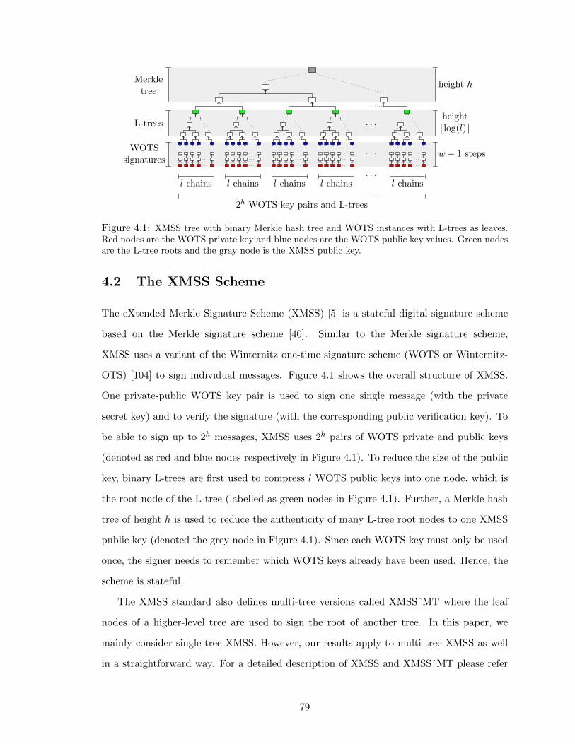
l chains l chains l chains l chains l chains
. . .
. . .
. . .
2h WOTS key pairs and L-trees
WOTSsignatures
L-trees
Merkletree
w − 1 steps
heightdlog(l)e
height h
Figure 4.1: XMSS tree with binary Merkle hash tree and WOTS instances with L-trees as leaves.Red nodes are the WOTS private key and blue nodes are the WOTS public key values. Green nodesare the L-tree roots and the gray node is the XMSS public key.
4.2 The XMSS Scheme
The eXtended Merkle Signature Scheme (XMSS) [5] is a stateful digital signature scheme
based on the Merkle signature scheme [40]. Similar to the Merkle signature scheme,
XMSS uses a variant of the Winternitz one-time signature scheme (WOTS or Winternitz-
OTS) [104] to sign individual messages. Figure 4.1 shows the overall structure of XMSS.
One private-public WOTS key pair is used to sign one single message (with the private
secret key) and to verify the signature (with the corresponding public verification key). To
be able to sign up to 2h messages, XMSS uses 2h pairs of WOTS private and public keys
(denoted as red and blue nodes respectively in Figure 4.1). To reduce the size of the public
key, binary L-trees are first used to compress l WOTS public keys into one node, which is
the root node of the L-tree (labelled as green nodes in Figure 4.1). Further, a Merkle hash
tree of height h is used to reduce the authenticity of many L-tree root nodes to one XMSS
public key (denoted the grey node in Figure 4.1). Since each WOTS key must only be used
once, the signer needs to remember which WOTS keys already have been used. Hence, the
scheme is stateful.
The XMSS standard also defines multi-tree versions called XMSSˆMT where the leaf
nodes of a higher-level tree are used to sign the root of another tree. In this paper, we
mainly consider single-tree XMSS. However, our results apply to multi-tree XMSS as well
in a straightforward way. For a detailed description of XMSS and XMSSˆMT please refer
79

to IETF RFC 8391 [5] and to [100].
In the following we briefly introduce the XMSS address scheme, WOTS, the L-tree con-
struction, and the procedure for constructing the Merkle tree. We also give an introduction
to XMSS key generation, signing, and verification.
Address Scheme. XMSS uses a hash-function address scheme throughout the Merkle
tree, L-tree, and WOTS computations to uniquely identify each individual step in the
overall graph. These addresses are used to derive keys for keyed hash functions that are
unique for each specific location in the tree. Each address is composed of eight 32-bit fields,
with fields for, e.g., the level within a tree and the leaf index. In total, an XMSS address
has a size of 256-bit. For more details about the hash function address scheme, please refer
to IETF RFC 8391 [5, Sect. 2.5].
Winternitz OTS. The WOTS scheme was first mentioned in [40]. For signing a message
digest D of n-byte length, WOTS uses a cryptographically secure hash function with n-
byte output strings to compute hash chains. The message digest is interpreted as binary
representation of an integer d. First, d is split into l1 = d8n/ log2(w)e base-w words di, 0 ≤
i < l1 and a checksum c =∑l1
i=0w−1−di is computed for these base-w words (w is called the
“Winternitz parameter”). The checksum c is split into l2 = blog2(l1(w − 1))/ log2(w)) + 1c
base-w words ci, 0 ≤ i < l2 as well. WOTS key generation, signing, and verification are
performed as follows:
• To create a private/public WOTS key pair, Alice computes l = l1 + l2 secret strings
s0,i for 0 ≤ i < l, each of n-byte length (for example using a secret seed and a PRF).
These l n-byte strings are the private WOTS key. Then, Alice uses a chaining function
to compute l hash chains of length w−1, hashing each s0,i iteratively w−1 times. The
resulting chain-head values sw−1,i, 0 ≤ i < l of n-byte length are the public WOTS
key of Alice.
• To sign a message digest, d is split into l1 base-w words together with l2 base-w check-
sum values computed as described above, Alice (re-)computes the intermediate chain
values (sd0,0, sd1,1, . . . , sdl1−1,l1−1, sc0,0, sc1,1, . . . , scl2−1,l2−1) starting from her private
key values. These l = l1 + l2 values are the signature.
80
• When Bob wants to verify the signature, he recomputes the remaining chain steps by
applying w− 1− di hash-function iterations to signature value sdi,0 and compares the
results with the corresponding public key values. If all chain-head values match the
public WOTS key, the signature is valid.
XMSS uses a modified WOTS scheme, sometimes referred to as WOTS+ or as W-OTS+ [105];
we use the term WOTS+ only when a explicit distinction from “original” WOTS is required
for clarification. WOTS+ uses a function chain() as chaining function that is a bit more
expensive than the simple hash-chain function described above. The function chain() uses
a keyed pseudo-random function prfk : {0, 1}256 7→ {0, 1}8n and a keyed hash-function
fk′ : {0, 1}8n 7→ {0, 1}8n. Within each chain step, the function chain() first computes a
unique n-byte key k′ and a unique n-byte mask using the prfk() function. The input to
prfk() is the hash function address of the current step (including the chain step and a
marker for the usage as key or as mask). The key k for prfk() is a seed that is part of the
XMSS public key. The mask is then XOR-ed with the n-byte output from the previous
chain-function call (or the initial WOTS+ chain n byte input string) and the result is used
as input for the hash-function f() under the key k′, which gives the n-byte output of the
chaining function chain() in the last iteration step.
The WOTS+ secret key consists of l (l is defined as described above for WOTS) pseudo-
random strings of n-bytes in length. The XMSS specification does not demand a certain
function to compute the WOTS+ private key. In the XMSS reference implementation, they
are generated using the prfk() function with the local address (including the chain index)
as input and keyed with the XMSS secret key seed. Each WOTS+ secret key maps to
one corresponding WOTS+ public key, which is computed by calling the chaining function
chain() with w − 1 iteration steps. Signing and verification in WOTS+ work as described
above for WOTS using the WOTS+ chaining function. The more complex structure of the
chaining function of WOTS+ compared to WOTS is required for multi-target resistance
and within the XMSS security proof.
L-Tree. The leaf nodes of an XMSS tree are computed from the WOTS+ public keys by
using an unbalanced binary tree of l leaf nodes (one leaf node for each WOTS+ public key
81

value), hence called L-tree. The nodes on each level of the L-tree are computed by hashing
together two nodes from the lower level. A tree hash function hashrand : {0, 1}8n×{0, 1}8n 7→
{0, 1}8n is used for this purpose.
The function hashrand() uses the keyed pseudo-random function prfk() and a keyed
hash-function hk′′ : {0, 1}16n 7→ {0, 1}8n. First, an n-byte key k′′ and two n-byte masks
are computed using the prfk() with the address (including the L-tree level and node index)
as input and the same public seed as used for WOTS+ as key. The masks are then each
XOR-ed to the two n-byte input strings representing the two lower-level nodes and the
results are concatenated and used as input for the hash-function h() keyed with k′′, which
gives the n-byte output of the tree hash function hashrand().
To be able to handle the pairwise hashing at levels with an odd number of nodes, the
last node on these levels is lifted to a higher level until another single node is available. The
root of the L-tree gives one single hash-value, combining the l WOTS+ public keys into one
WOTS+ public key.
XMSS Merkle Tree. In order to obtain a small public key, the authenticity of many
WOTS public keys (i.e., L-tree root keys) is reduced to one XMSS public key using a
binary Merkle tree. Similar to the L-tree construction described above, on each level of the
binary tree, neighbouring nodes are pairwise hashed together using the hashrand() function
to obtain one single root node that constitutes the XMSS public key (see Figure 4.1).
4.2.1 Key Generation
XMSS key generation is quite expensive: In order to compute the XMSS public key, i.e., the
root node of the Merkle tree, the entire XMSS tree needs to be computed. Depending on
the height h of the tree, thousands to millions of hash-function calls need to be performed.
As shown in Figure 4.1, XMSS key generation starts by generating 2h leaf nodes of the
Merkle tree. Each leaf node consists of an WOTS instance together with an L-tree. For
each WOTS instance, first l WOTS private keys are generated. These are then used to
compute the l WOTS chains to obtain l WOTS public keys and then the L-trees on top of
these. Once all 2h L-tree root nodes have been computed, the Merkle tree is computed to
82
obtain the XMSS public key.
The XMSS public key consists of the n-byte Merkle tree root node and the n-byte
public seed required by the verifier to compute masks and public hash-function keys using
the function prfk() within the WOTS-chain, L-tree, and Merkle tree computations. The
XMSS standard does not define a format for the XMSS private key. In the XMSS reference
implementation that accompanies the standard, an n-byte secret seed is used to generate
the WOTS secret keys using a pseudo random function (e.g., prfk()).
4.2.2 Signature Generation and Verification
XMSS is a stateful signature scheme: Each WOTS private/public key pair must be used
only once; otherwise, the scheme is not secure. To determine which WOTS key pair already
has been used, an n-byte leaf index (the state) is stored with the private key. The index
defines which WOTS key pair will be used for the next signature; after each signature
generation, the index must be increased.
Similar to most signature schemes, for signing an arbitrary-length message or a docu-
ment M , first a message digest of M is computed; details can be found in [5, Sect. 4.1.9].
The digest M ′ is then signed using the selected WOTS instance. This results in l n-byte
values corresponding to the base-w decomposition of M ′ including the corresponding check-
sum. Furthermore, in order to enable the verifier to recompute the XMSS public root key
from a leaf node of the Merkle tree, the signer needs to provide the verification path in the
Merkle tree, i.e., h n-byte nodes that are required for the pairwise hashing in the binary
Merkle tree, one node for each level in the Merkle tree.
Therefore, in the worst case, the signer needs to recompute the entire XMSS tree in
order to select the required nodes for the verification path. There are several optimization
strategies using time-memory trade-offs to speed up signature generation. For example,
the signer can store all nodes of the Merkle tree up to level h′ alongside the private key.
Then, when signing, the signer only needs to compute an (h−h′)-height sub-tree including
the WOTS leaves and can reproduce the signature path for the remaining h′ levels from
the stored data. Other algorithms with different trade-offs exist; for example the BDS tree
traversal algorithm [106] targets at reducing the worst case runtime of signature generation
83

by computing a certain amount of nodes in the Merkle tree at each signature computation
and storing them alongside the XMSS state.
Compared to key generation, XMSS signature verification is fairly inexpensive: An
XMSS public key contains the Merkle root node and the public seed. An XMSS signature
contains the WOTS leaf index, l WOTS-signature chain values, and the verification path
consisting of h Merkle-tree pair values, one for each level in the tree. The verifier computes
the message digest M ′ and then recomputes the WOTS public key by completing the
WOTS chains and computing the L-tree. The verifier then uses the Merkle-tree pair values
to compute the path through the Merkle tree and finally compares the Merkle tree root
node that was obtained with the root node of the sender’s public key. If the values are
equal, verification succeeds and the signature is sound; otherwise verification fails and the
signature is rejected.
4.2.3 Security Parameters
RFC 8391 [5] defines parameter sets for the hash functions SHA-2 and SHAKE targeting
classical security levels of 256-bit with n = 32 and 512-bit with n = 64 in order to provide
128-bit and 256-bit of security respectively against attackers in possession of a quantum
computer [5, Sect. 5]. The required parameter sets, as specified in [5, Sect. 5.2], all use
SHA-256 to instantiate the hash functions (SHA-512 and SHAKE are optional). Therefore,
for this work, we focus on the SHA-256 parameter sets with n = 32.
In this case, the keyed hash functions prfk : {0, 1}256 7→ {0, 1}256, fk′ : {0, 1}256 7→
{0, 1}256, and hk′′ : {0, 1}512 7→ {0, 1}256, are implemented by computing the input to
SHA-256 as concatenation of:
• a 256-bit hash-function specific domain-separator,
• the 256-bit hash-function key, and
• the 256-bit or 512-bit hash-function input.
For SHA-256, three different parameter sets are provided in RFC 8391 [5, Sect. 5.3], all
with n = 32 and w = 16 but with h = 10, h = 16, or h = 20. In general, a bigger tree height
h leads to an exponential growth in the run time of key generation. For verification the run
84

time is only linearly impacted. The naive approach for signing requires one to recompute
the entire tree and thus is as expensive as key generation. However, by use of the BDS
tree traversal algorithm [106], the tree height has only a modest impact on the run time.
Multi-tree versions of XMSS (XMSSˆMT) can be used to speed up the computations at
the cost of larger signature sizes (e.g., to improve key generation and signing performance
or to achieve a larger h). We are using h = 10 throughout our experiments; however, our
implementation is not restricted to this value.
4.3 The SHA-256 Hash Function
The hash function SHA-256 [107] computes a 256-bit hash value from a variable-length
input. SHA-256 uses a 256-bit internal state that is updated with 512-bit blocks of the
input. Therefore, SHA-256 defines a padding scheme for extending variable-length inputs
to a multiple of 512-bit. SHA-256 works as follows:
• Initialize the internal state with a well-defined Initialization Vector (IV) (see [107, Sect.
4.2.2] for details).
• Extend the `-bit input message with a padding to make the length of the padded
input a multiple of 512-bit:
– append a single 1-bit to the input message, then
– append 0 ≤ k 0-bit such that ` + 1 + k + 64 is minimized and is a multiple of
512, and finally
– append ` as a 64-bit big-endian integer.
• Iteratively apply a compression function to all 512-bit blocks of the padded input and
the current internal state to obtain the next updated internal state.
• Once all 512-bit blocks have been processed, output the current internal state as the
hash value.
The compression function uses the current internal state and a 512-bit input block and
outputs an updated internal state. For SHA-256, the compression function is composed of
64 rounds.
85

4.4 Software Implementation and Optimization
We use the official XMSS reference implementation1 as software-basis for this work. We
applied minor modifications to the XMSS reference code to link it against the mbed TLS
library2 instead of OpenSSL, because mbed TLS generally is more suitable for resource-
restricted embedded platforms such as the Murax SoC platform and its SHA-256 imple-
mentation has less library-internal dependencies than that of OpenSSL, which simplifies
stand-alone usage of SHA-256.
The tree-hash algorithm [5] used for computing the XMSS public key and the authenti-
cation path within the Merkle tree requires an exponential number of 2h WOTS operations
for computing tree leaves. However, key generation and signing are not memory intensive
when the tree is computed with a depth-first strategy.
The XMSS reference implementation provides two algorithms for signature generation.
The first approach (implemented in file “xmss core.c”) straightforwardly re-computes all
tree leaf nodes in order to compute the signature authentication path and therefore has
essentially the same cost as key-generation. This approach does not require to store any
further information. The second approach (implemented in file “xmss core fast.c”) uses the
BDS algorithm [106] to make a trade-off between computational and memory complexity.
It requires to additionally store a state along the private key. Both versions can be used
with our hardware accelerators. Our experiments show that both versions of the signature
generation algorithm run smoothly on the Murax SoC. Even with the additional storage
requirement, running all the operations of XMSS with the BDS-based signature algorithm
leads to reasonable memory usage, as shown in Section 4.12. Since the runtime of the basic
signature algorithm is almost identical to key generation, we are using the fast BDS version
of the signature algorithm [106] for our performance reports.
To have a fair reference point for the comparison of a pure software implementation with
our hardware accelerators, we implemented two software optimizations for the XMSS refer-
ence software implementation as described in the following paragraphs. These optimizations
1. https://github.com/joostrijneveld/xmss-reference/, commit 06281e057d9f5d
2. https://tls.mbed.org/
86

prf
sha256 compression
thash h
wots sign
hash1024 hash768
expand seed
treehash/bds
xmss keypair xmss verifyxmss sign
wots pkgen
SHA256
thash f
gen chain
wots pk from sigl tree
Figure 4.2: Simplified XMSS call graph. Function calls removed during software optimization (i.e.,calls to SHA-256 including init, update, and finish) are displayed with dotted nodes and arrows.Meanwhile, added calls are displayed with dashed nodes and arrows. The “fixed input length”optimization is marked in blue, the “pre-computation” optimization is marked in green.
are also helpful on other processor architectures but only work for SHA-256 parameter sets,
because they depend on the specific SHA-256 block size and padding scheme.
Figure 4.2 shows a simplified XMSS call graph for both the original source code version
and the changes that we applied for optimizations as described below.
4.4.1 Fixed Input Length
In the XMSS software reference implementation, around 90% of the time is spent inside the
hash-function calls. Therefore, the SHA-256 function is most promising for optimization
efforts. In particular for short-length inputs, a significant overhead is caused by computing
the SHA-256 padding. However, within the XMSS scheme, the inputs of almost all SHA-256
calls have a well-known, fixed length: A general, arbitrary-length SHA-256 computation is
only required when computing the actual hash digest of the input message, which is called
only once for signing and once for verifying. For all the other SHA-256 calls, the length of
the input data is either 768-bit or 1024-bit depending on where SHA-256 is called within
the XMSS scheme: An input length of 768-bit is required within the PRF and within the
WOTS-chain computation; an input length of 1024-bit is required within the Merkle tree
and the L-trees to hash two nodes together. Therefore, we can eliminate the overhead
87

for the padding computation of the SHA-256 function by “hardcoding” the two required
message paddings, given that their lengths are known beforehand.
We implemented two specialized SHA-256 functions: The function hash768 targeting
messages with a fixed length of 768-bit and hash1024 targeting messages with fixed length
of 1024-bit. Figure 4.3 shows the padding for hash768 and hash1024. Since SHA-256
has a block size of 512-bit, two blocks are required to hash a message of length 768-bit.
Therefore, we need to hardcode a 256-bit padding for hash768 to fill up the second block
to 512-bit. When a 768-bit message is fed to the hash768 function, the 256-bit padding is
appended to the message. Then, the new 1024-bit padded message is divided into two 512-
bit blocks and the compression function is performed on each of them one by one. Once the
compression function on the second message block has finished, the internal state is read out
and returned as the output. The SHA-256 standard always demands to append a padding
even if the input length is a multiple of 512-bit. Therefore, for the hash1024 function
a 512-bit padding is hardcoded similarly to hash768 and three calls to the compression
function are performed. The main interface to SHA-256 in mbed TLS has three functions,
mbedtls_sha256_init, mbedtls_sha256_update, and mbedtls_sha256_finish
(combined and simplified to SHA256 in Figure 4.2). The “init”-function initializes the
internal state of the SHA-256 implementation. The “update”-function allows to feed in
message chunks of arbitrary size and updates the internal state accordingly. The “finish”
function finally adds the padding and returns the message digest. Internally, these functions
need to adapt arbitrary-length message chunks to the SHA-256 input block size of 512-bit:
If the size of message-chunk input to the update function mbedtls_sha256_update is
not a multiple of 512-bit, the remaining data is buffered alongside the internal state and
used either in the next “update” or in the final “finish” call.
The SHA-256 implementation of mbed TLS is intended to hash messages of an arbitrary
length: When the “finish” function is called, the actual length of the entire message is
computed as sum over the lengths of all individual message chunks and the padding is
generated accordingly. However, within the XMSS scheme, the inputs of almost all SHA-
256 calls have a well-known, fixed length: A general, arbitrary-length SHA-256 computation
is only required when computing the actual hash digest of the input message, which is called
88

256-bit hash768-padding:
0x80 0x00 . . . 0x00 0x03 0x00
512-bit hash1024-padding:
0x80 0x00 . . . 0x00 0x00 0x00 0x00 . . . 0x00 0x04 0x00
7 0 15 8 239 232 247 240 255 248
7 0 15 8 239 232 247 240 255 248 263 256 495 448 503 496 511 504
Figure 4.3: Fixed padding for hash768 and hash1024.
only once for signing and once for verifying. For all the other SHA-256 calls, the length of
the input data is either 768-bit or 1024-bit depending on where SHA-256 is called within
the XMSS scheme: An input length of 768-bit is required within the PRF and within the
WOTS-chain computation; an input length of 1024-bit is required within the Merkle tree
and the L-trees to hash two nodes together. Therefore, we can eliminate the overhead
for the padding computation of the SHA-256 function by “hardcoding” the two required
message paddings, given that their lengths are known beforehand.
Software Implementation. We implemented two specialized SHA-256 functions: The
function hash768 targeting messages with a fixed length of 768-bit and function hash1024
targeting messages with fixed length of 1024-bit. Figure 4.3 shows the padding for hash768
and hash1024. Since SHA-256 has a block size of 512-bit, two blocks are required to hash a
message of length 768-bit. Therefore, we need to hardcode a 256-bit padding for hash768 to
fill up the second block to 512-bit. When a 768-bit message is fed to the hash768 function,
the 256-bit padding is appended to the message. Then, the new 1024-bit padded message
is divided into two 512-bit blocks and the compression function is performed on each of
them one by one. Once the compression function on the second message block has finished,
the internal state is read out and returned as the output. The SHA-256 standard always
demands to append a padding even if the input length is a multiple of 512-bit. Therefore,
for the hash1024 function a 512-bit padding is hardcoded similarly to hash768 and three
calls to the compression function are performed.
Evaluation. Table 4.1 shows a comparison of the original XMSS reference implementation
with an optimized version making use of the “fixed input length” optimization on the Murax
SoC with parameters n = 32, w = 16 and h = 10. The speedup for 768-bit inputs is about
89

1.07× and for 1024-bit inputs is about 1.04×. The use of 768-bit inputs is more common
during the XMSS computations. Therefore, we see an about 1.06× speedup for WOTS
computations as well as the key generation, signing, and verification operations in XMSS.
4.4.2 Pre-Computation
Pre-computation is commonly referred to as the act of performing an initial computation
before runtime to generate a lookup table to avoid repeated computations during runtime.
This technique is useful in improving real-time performance of algorithms at the expense of
extra memory and extra preparatory computations [108]. In XMSS, a variant of this idea
can be applied to improve the performance of the hash functions.
Within XMSS, SHA-256 is used to implement four different keyed hash-functions, the
function thash_f for computing f() in the WOTS-chains, the function thash_h for h()
in the tree hashing, and the function prf for computing the prf(), generating masks and
hash-function keys. Furthermore, SHA-256 is used to compute the message digest that is
signed using a WOTS private key. The domain separation and the keying for these four
functions are achieved by computing the input to SHA-256 as the concatenation of a 256-bit
domain separator value (distinct for these four functions), the 256-bit hash key, and the
hash-function input. Since SHA-256 operates on 512-bit blocks, one entire block is required
for domain separation and keying of the respective hash function.
In case of the prf, for all public-key operations when generating masks and hash-
function keys for the WOTS chain, the L-tree and Merkle tree operations, the key to the
prf is the 256-bit XMSS public seed. Thus, both the 256-bit domain separator and the
256-bit hash-function key are the same for all these calls for a given XMSS key pair. These
two parts fit exactly into one 512-bit SHA-256 block. Therefore, the internal SHA-256
state after processing the first 512-bit block is the same for all these calls to the prf and
based on this fact, we can save one SHA-256 compression function call per prf-call by pre-
computing and replaying this internal state. The internal state can either be computed once
and stored together with the XMSS key or each time an XMSS operation (key generation,
signing, verification) is performed. This saves the computation on one of the two input
blocks in hash768 used in the prf. For hash1024, this optimization is not applicable
90

“original” + “fixed input length” + “pre-computation”Cycles Cycle Speedup Cycles Speedup Speedup
(A) (B) (AB) (C) (BC) (AC)
hash768 11.5× 10³ 10.7× 10³ 1.07 5.87× 10³ 1.83 1.95hash1024 16.2× 10³ 15.6× 10³ 1.04 — — —
WOTS-chain 571 × 103 530 × 103 1.08 371 × 103 1.43 1.54XMSS-leaf 42.2× 10⁶ 39.8× 10⁶ 1.06 27.7 × 10⁶ 1.44 1.53
key generation 43.3× 10⁹ 40.8× 10⁹ 1.06 28.3 × 10⁹ 1.44 1.53signing 58.3× 10⁶ 55.0× 10⁶ 1.06 38.4 × 10⁶ 1.43 1.52verification 26.7× 10⁶ 25.2× 10⁶ 1.06 17.4 × 10⁶ 1.45 1.54
Table 4.1: Cycle count and speedup of the “fixed input length” optimization and for both, the“fixed input length” and the “pre-computation” optimizations, on the Murax SoC with parametersn = 32, w = 16 and h = 10.
since the fixed input block pattern does not exist.
Software Implementation. At the first call to prf, we store the SHA-256 context of
mbed TLS for later usage after the first compression function computation. The state in-
cludes the internal state and further information such as the length of the already processed
data. When the prf is called during XMSS operations, we first create a copy of the initially
stored prf SHA-256 context and then perform the following prf() operations based on this
state copy, skipping the first input block. The cost for the compression function call on
the first SHA-256 block within the prf is therefore reduced to a simple and inexpensive
memory-copy operation.
Evaluation. Performance measurements and speedup for our pre-computation optimiza-
tion are shown in Table 4.1. For hash768 we achieve a 1.83× speedup over the “fixed input
length” optimization (column “Speedup (BC)”), because only one SHA-256 block needs to
be processed instead of two. Compared to the original non-optimized version, with both
optimizations (including “fixed input length”) enabled we achieve an almost 2× speedup
(column “Speedup (AC)”).
The function thash_f for computing WOTS-chains requires two calls to the prf (each
on two SHA-256 blocks) for generating a key and a mask and one call to hash768 (on two
SHA-256 blocks). Without pre-computation, six calls to the SHA-256 compression function
are required. With a pre-computed initial state for the prf, only four calls to the SHA-
91
256 compression function are required, saving one third of the compression function calls.
This optimization leads to a 1.43× speedup for WOTS-chain computations (row “WOTS-
chain”, column “Speedup (BC)”). The overall speedup including both optimizations “pre-
computation” and “fixed input length” is 1.54×.
For L-tree computations within the randomized tree-hash function thash_h, there are
three calls to the prf (each on two SHA-256 blocks) for computing two masks and one
hash-function key and one call to hash1024 (on three SHA-256 blocks). Without pre-
computation, nine calls to the SHA-256 compression function are required. With a pre-
computed initial state for the prf, only six calls to the SHA-256 compression function are
required, again saving one third of the compression function calls. This optimization leads to
a 1.44× speedup for the overall XMSS leaf computations (see Table 4.1, row “XMSS-leaf”).
The speedup including both optimizations is around 1.53×.
The expected speedup for Merkle tree computations is about the same as for the L-tree
computations since the trees are constructed in a similar way. Table 4.1 shows that we
achieve an overall speedup of more than 1.5× including both optimizations also for the
complete XMSS operations, i.e., key generation, signing, and verification. We observed a
similar speedup on an Intel i5 CPU. Similar speedups can be achieved on other architectures
as well, e.g., ARM processors.
4.5 Open-Source RISC-V Based Platform
The RISC-V instruction set architecture (ISA) is a free and open architecture, overseen by
the RISC-V Foundation with more than 100 member organizations3. It is an open standard
instruction set architecture (ISA) based on established reduced instruction set computer
(RISC) principles. The most distinguishing feature of RISC-V, when compared to other
ISA designs, is that the RISC-V ISA is provided under open source licenses that are free for
use. It has a modular design, consisting of base sets of instructions with optional instruction
set extensions.
The RISC-V project began in 2010 at the University of California, Berkeley, with the
3. https://riscv.org/
92

initial goal of providing open-sourced and practical design for research and education. Over
the past decade, many volunteer contributors from both academia and industry have joined
the project, and now there are a wide range of available RISC-V CPU and SoC imple-
mentations. Many of these CPU/SoC designs are increasingly being used for commercial
designs. For example, different series of RISC-V SoCs developed by SiFive [109], Berkeley’s
Rocket Chip [110], Ibex RISC-V core based on LowRISC [111], XuanTie [112] developed
by Alibaba, and the VexRiscv CPU. All of these RISC-V architectures have been applied
successfully for practical use cases. For prototyping our hardware designs, the VexRiscv
CPU and the SoC platform extended based on it have been used intensively. The details of
the VexRiscv CPU and the SoC based on it are provided in the following text.
4.5.1 VexRiscv CPU
First-prize winner in the RISC-V Soft-Core CPU Contest of 20184, VexRiscv5 is a 32-bit
RISC-V CPU implementation written in SpinalHDL6, which is a Scala-based high-level
hardware description language. It supports the RV32IM instruction set and implements a
five-stage in-order pipeline. The design of VexRiscv is very modular: All complementary
and optional components are implemented as plugins and therefore can easily be integrated
and adapted into specific processor setups as needed. The VexRiscv ecosystem provides
memories, caches, IO peripherals, and buses, which can be optionally chosen and combined
as required.
4.5.2 Murax SoC
The VexRiscv ecosystem also provides a complete predefined processor setup called “Murax
SoC” that has a compact and simple design and aims at small resource usage. The Murax
SoC integrates the VexRiscv CPU with a shared on-chip instruction and data memory, an
Advanced Peripheral Bus (APB), a Joint Test Action Group (JTAG) programming inter-
4. https://riscv.org/2018/10/risc-v-contest/
5. https://github.com/SpinalHDL/VexRiscv/
6. https://spinalhdl.github.io/SpinalDoc/
93

face, and a Universal Asynchronous Receiver-Transmitter (UART) interface. It has very
low resource requirements (e.g., only 1350 ALMs on a Cyclone V FPGA) and can oper-
ate on its own without any further external components. The simple design and compact
size of Murax SoC have made this architecture an ideal candidate for resource-constrained
embedded applications.
Due to its modular design, the RISC-V ISA becomes an increasingly popular architecture
for embedded systems. It is used, e.g., as a control processor in GPUs and in storage
devices [113], for secure boot and as USB security dongle [114], and for building trusted
execution environments (TEE) with secure hardware enclaves [115]. Since the RISC-V ISA
is an open standard, researchers and industry can easily extend and adopt it in their designs
without IP constraints.
4.6 Software-Hardware Co-Design of XMSS
Software-hardware co-design has been adopted as a common discipline for designing embed-
ded system architectures since the 1990s [116]. By combining both software and hardware
in an embedded system, a trade-off between software flexibility and hardware performance
can be achieved depending on the user’s needs. To accelerate XMSS computations, we
developed a software-hardware co-design of XMSS by moving the most compute-intensive
operations to hardware while keeping the rest of the operations running in software.
4.6.1 Prototype Platform
In our work, we use the open-sourced Murax SoC as the prototype platform. Murax SoC
is the smallest open-source SoC that fits to our target of embedded applications. When
synthesized on an Artix 7 FPGA, only 1128 LUTs and 1219 FFs are needed. It even fits on
tiny FPGAs like the Lattice ICE40 FPGA. Other RISC-V SoCs have much larger resource
requirements, e.g., the Rocket Chip SoC [110], when synthesized on a Zynq ZC706 FPGA,
requires 36395 LUTs and 22199 FFs. We can expect a better performance on bigger RISC-V
platforms, however, the time-area product will be much worse.
Murax SoC vs. ARM Cortex-M3. The performance of the Murax SoC is comparable to
94

an ARM Cortex-M3: A multi-tree version of XMSS has been implemented on an embedded
ARM Cortex-M3 platform in [117] (see also Section 4.13.3). We compiled a pure C-version
of the code from [117] for both an ARM Cortex-M3 processor and the Murax SoC and
compared their performance (see the bottom lines of Table 4.7). In terms of cycle count,
the Cortex-M3 is only about 1.5× faster than the Murax SoC. Therefore, we conclude
that the Murax SoC is a good representative for an embedded system processor with low
resources. As opposed to an ARM Cortex-M3 platform, however, the Murax SoC is fully
free, open, and customizable and thus is an ideal platform for our work.
4.6.2 Interfaces Between Software and Hardware
Extending the Murax SoC with new hardware accelerators can be implemented easily in
a modular way using the APB bus. We used this feature for our XMSS accelerators.
Depending on different use cases, our open-source software-hardware co-design of XMSS
can be migrated to other RISC-V or embedded architectures with small changes to the
interface. The hardware accelerators are connected to the APB using a bridge module: The
Apb3Bridge module connects on one side to the 32-bit data bus and the control signals of
the APB and on the other side to the hardware accelerator. It provides a 32-bit control
register, which is mapped to the control and state ports of the hardware accelerator, and
data registers for buffering the input data, which are directly connected to the input ports of
the hardware accelerator. The control and data registers are mapped to the APB as 32-bit
words using a multiplexer, selected by the APB address port on APB write; the control
register and the output ports of the hardware accelerator are connected in the same way to
be accessed on APB read. This allows the software to communicate with the accelerators
via memory-mapped IO using simple load and store instructions.
Software Modifications. We modified the corresponding software functions in the op-
timized XMSS implementation to replace them with function calls to our hardware accel-
erators as follows: The function first sets control bits (e.g., RESET, INIT) to high in the
control register. When these bits are received as high by the Apb3Bridge module, it raises
the corresponding input signals of the hardware accelerator. Similarly, the input data is
95
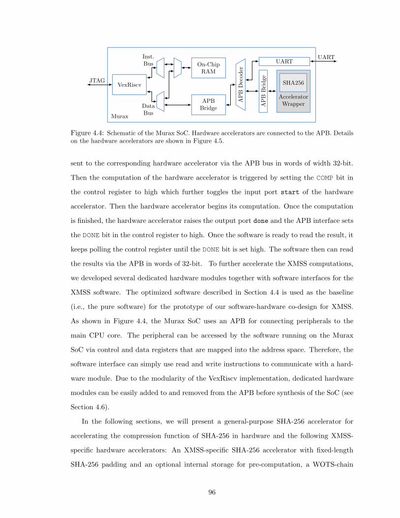
VexRiscv
On-ChipRAM
APBBridge
AP
BD
ecoder
UART
AP
BB
ridge
AcceleratorWrapper
SHA256
Inst.Bus
DataBus
JTAG
UART
Murax
Figure 4.4: Schematic of the Murax SoC. Hardware accelerators are connected to the APB. Detailson the hardware accelerators are shown in Figure 4.5.
sent to the corresponding hardware accelerator via the APB bus in words of width 32-bit.
Then the computation of the hardware accelerator is triggered by setting the COMP bit in
the control register to high which further toggles the input port start of the hardware
accelerator. Then the hardware accelerator begins its computation. Once the computation
is finished, the hardware accelerator raises the output port done and the APB interface sets
the DONE bit in the control register to high. Once the software is ready to read the result, it
keeps polling the control register until the DONE bit is set high. The software then can read
the results via the APB in words of 32-bit. To further accelerate the XMSS computations,
we developed several dedicated hardware modules together with software interfaces for the
XMSS software. The optimized software described in Section 4.4 is used as the baseline
(i.e., the pure software) for the prototype of our software-hardware co-design for XMSS.
As shown in Figure 4.4, the Murax SoC uses an APB for connecting peripherals to the
main CPU core. The peripheral can be accessed by the software running on the Murax
SoC via control and data registers that are mapped into the address space. Therefore, the
software interface can simply use read and write instructions to communicate with a hard-
ware module. Due to the modularity of the VexRiscv implementation, dedicated hardware
modules can be easily added to and removed from the APB before synthesis of the SoC (see
Section 4.6).
In the following sections, we will present a general-purpose SHA-256 accelerator for
accelerating the compression function of SHA-256 in hardware and the following XMSS-
specific hardware accelerators: An XMSS-specific SHA-256 accelerator with fixed-length
SHA-256 padding and an optional internal storage for pre-computation, a WOTS-chain
96

accelerator for the WOTS chaining computations, and an XMSS-leaf generation accelerator
combining WOTS and L-tree computations.
4.7 General Purpose SHA-256 Accelerator
Since around 90% of the time is spent performing the SHA-256 computations in the XMSS
reference implementation, the first hardware module we developed is the SHA256 module,
which is a general-purpose hash accelerator that accepts variable length inputs. The SHA256
module is used as the building block in the XMSS-specific hardware accelerators described
in the following sub-sections. It has a similar interface as the generic SHA-256 compression
function in software: It receives a 512-bit data block as input and computes the compression
function, updating an internal 256-bit state. This state can be read out as the 256-bit digest
when the SHA-256 computation is finished. Padding is performed in software as before.
4.7.1 Hardware Implementation
We developed the module SHA256 by implementing an iterative version of SHA-256 by
computing one round of SHA-256 in one clock cycle. Therefore, we require 64 clock cycles
to process one SHA-256 data block. This provides a good trade-off between throughput
and area consumption similar to [118]. The SHA256 module is a generic hash core without
platform-specific optimizations that runs on any FPGA platform. Users can easily use a
platform-optimized SHA-256 core within our hardware modules, e.g., [119–121].
The software optimization of SHA-256 exploiting fixed input lengths of the SHA-256
function described in Section 4.4.1 can be mapped in a straightforward way to the SHA256
module. The software prepares the SHA-256 input chunks with pre-defined paddings just as
before and then transfers each chunk to the SHA256 module for processing. Therefore, the
speedup achieved in the software version can also be exploited for this hardware accelerator.
In order to support the “pre-computation” optimization, (Section 4.4.2), we added an
interface to the SHA256 module that allows to set the internal state of the SHA256 module
from software. Reading the internal state is the same as reading the SHA-256 message
97

Design Cycles Area Reg. Fmax Time Time×Area Speedup(ALM) (MHz) (µs) (relative)
one 512-bit blockSHA256 64 1180 1550 100 0.639 — —
hash768 with pre-computation (one 512-bit block)Murax 4950 1350 1660 152 32.6 9.22 1.00+ SHA256 253 2860 3880 99.9 2.53 1.00 12.9
hash768 without pre-computation (two 512-bit blocks)Murax 10,700 1350 1660 152 70.4 8.76 1.00+ SHA256 576 2860 3880 99.9 5.77 1.00 12.2
hash1024 (three 512-bit blocks)Murax 15,600 1350 1660 152 102 10.5 1.00+ SHA256 700 2860 3880 99.9 7.01 1.00 14.6
Table 4.2: Performance of the hardware module SHA256 and comparisons of performing the SHA-256compression function on different numbers of 512-bit blocks when called from the RISC-V softwareon a Murax SoC and on a Murax SoC with a SHA256 accelerator (all using the “fixed input length”optimization in software, i.e., cost for SHA-256 padding is not included).
digest at the end of the hash computation.
Software Support for Hardware. We modified the function mbedtls_sha256_init
from mbed TLS to replace the software implementation of the SHA-256 compression func-
tion with a call to our hardware accelerator as follows: The function first sets the INIT
bit to high in the control register. When this bit is received as high by the Apb3Bridge
module, it raises the init message signal of the SHA256 module, which resets the value
of internal state register to the SHA-256 initialization value. In order to set the internal
state for the pre-computation optimization, the software writes a previously stored state to
the data register and then sets the control register bit LOAD_IV to high. Once the APB
interface sees this bit as high, it sets the init iv signal to high and the SHA256 module sets
the internal state to the 256 least significant bits of the input signal data in. When the
compression function is called in software, the 512-bit input message block is sent to the
SHA256 module via the APB bus in words of width 32-bit. Then, the SHA-256 computation
is triggered. While the hardware is performing the hash computation, the software can go
on transferring the next data block to the SHA256 module. This reduces the communication
overhead and increases the efficiency of the SHA256 module.
98

4.7.2 Evaluation
Table 4.2 shows performance, resource requirements, and maximum frequency of the SHA256
module. The module requires 64 cycles (one cycle per round) for computing the compression
function on one 512-bit input block. Table 4.2 also shows a comparison of computing one
SHA-256 compression function call in software (design Murax) with calling the hardware
module from the software (design “Murax + SHA256”). Transferring data to the SHA256
accelerator module and reading back the results contribute a significant overhead: The entire
computation on a 512-bit input block (without SHA-256 padding computation) requires
253 cycles. This overhead is due to the simple bus structure of the Murax SoC; a more
sophisticated bus (e.g., an AXI bus) may have a lower overhead – at a higher cost of
resources. However, we achieve an almost 13× speedup over the software implementation
of the SHA-256 compression function from the mbed TLS library which requires about 4950
cycles on the Murax SoC. For one regular hash768 function call, the SHA-256 compression
function needs to be performed on two 512-bit blocks, while for one hash1024 function
call, three 512-bit blocks are needed. When the “pre-computation” optimization is enabled
in the software, only one 512-bit block needs to be compressed in a hash768 function call.
Table 4.6 shows the performance impact of the SHA256 module on XMSS computations
(designs Murax and “Murax + SHA256”, including both “fixed input length” and “pre-
computation” software optimizations). For the key generation, signing and verification
operations, the SHA256 module accounts for an about 3.8× speedup in the XMSS scheme.
To further accelerate the XMSS computations in an efficient way, in the following we
describe the XMSS-specific hardware accelerators that we developed. We first describe an
XMSS-specific SHA-256 accelerator, which performs fixed-length SHA-256 padding and pro-
vides optional internal storage for one pre-computed state in hardware. Then, we describe
how we use this XMSS-specific SHA-256 accelerator as building-block for larger hardware
accelerators: An accelerator for WOTS-chain computations and an accelerator for XMSS-
leaf generation including WOTS and L-tree computations.
99

4.8 XMSS-specific SHA-256 Accelerator
In Section 4.4, we proposed two software optimizations for the XMSS scheme: “fixed in-
put length” for accelerating SHA-256 computations on 768-bit and 1024-bit inputs and
“pre-computation” for acceleration of the function prf(). For hardware acceleration, we
introduced a general-purpose SHA-256 hardware module in Section 4.7, which replaces the
SHA-256 compression function and thus naturally supports the “fixed input length” opti-
mization and the “pre-computation” optimization of the software implementation. How-
ever, both of the optimizations require to repeatedly transfer the same data, i.e., padding
or the pre-computed state, to the SHA256 module, e.g. the “pre-computation” optimiza-
tion requires to transfer the pre-computed internal state for each prf() computation. These
data transfers introduce an overhead. To eliminate this overhead and as building block for
the hardware accelerator modules described in the following sub-sections, we developed an
XMSS-specific SHA-256 accelerator, the SHA256XMSS module. It has a similar functionality
as the general SHA256 module; however, the SHA256XMSS module supports both of the soft-
ware optimizations internally: It only accepts complete input data blocks of size 768-bit or
1024-bit and adds the SHA-256 padding in hardware. In addition, it provides an optional
internal 256-bit register for storing and replaying a pre-computed state.
4.8.1 Hardware Implementation
We used the SHA256 module as building block for the implementation of the SHA256XMSS
module. All the SHA-256 compression computations in SHA256XMSS are done by interacting
with the SHA256 module. In order to handle larger input blocks, the data in port of the
SHA256XMSS module is 1024-bit wide. The SHA256XMSS module has an additional state
machine to autonomously perform two or three compression-function iterations (depending
on the input length). The state machine also takes care of appending the pre-computed
SHA-256 padding to the input data before the last compression function computation. To
select between different input lengths, the SHA256XMSS module has a message length input
signal (low for 768-bit, high for 1024-bit). To support the “pre-computation” optimization,
the SHA256XMSS module has a similar interface as described for the SHA256 module in
100
Section 4.7, which allows to set the internal state from software.
To further support the pre-computation functionality in hardware, a 256-bit register can
optionally be activated at synthesis time to the SHA256XMSS module for storing the fixed
internal state. An input signal store intermediate is added for requesting to store the
result of the first compression-function iteration in the internal 256-bit register. An input
signal continue intermediate is added for requesting to use the previously stored internal
state instead of the first compression iteration. The pre-computation functionality can be
enabled (marked as “+ PRECOMP” in the tables) or disabled at synthesis time in order to
save hardware resources for a time-area trade-off.
To reduce the latency of data transfer between the SHA256XMSS module and the soft-
ware, the SHA256XMSS module starts computation once the first input data block (512-
bit) is received. While the SHA256XMSS module is operating on the first input block,
the software sends the rest of the input data. An input signal second block available
is added which goes high when the rest of the input data is received. When a valid
second block available signal is received, the SHA256XMSS module starts the computation
on the rest of the input data once it finishes the previous computation.
When the SHA256XMSS module is added to the Murax SoC as a hardware accelerator, it
provides a SHA256 accelerator as well since the SHA256 module is used as its building block.
To achieve this, a hardware wrapper is designed (as shown in Figure 4.5) which includes
both the SHA256XMSS module and the SHA256 module. Apart from the control signals and
input data, the bridge module Apb3Bridge also takes care of forwarding a 3−bit cmd signal
from the software to the hardware wrapper. Depending on the value of cmd, the hardware
wrapper further dispatches the signals to the corresponding hardware module (SHA256XMSS
or SHA256) and triggers the computation. Similarly, based on the cmd value, the output
data from the corresponding module is returned. The design of the hardware wrapper brings
the flexibility that the SHA256XMSS module can not only accelerate XMSS-specific SHA-256
function calls, but also general SHA-256 function calls that accept variable length inputs,
which may be helpful for some other applications running in the system.
Software Support for Hardware. We replaced most of the SHA-256 function calls
101

Design Cycles Area Reg. Fmax Time Time×Area Speedup(ALM) (MHz) (µs) (relative)
two 512-bit blocksSHA256XMSS 128 1680 2070 89.7 1.43 1.77 1.00+ PRECOMP 64 1900 2320 98.3 0.651 1.00 2.19
three 512-bit blocksSHA256XMSS 192 1680 2070 89.7 2.14 — —
hash768Murax 10,700 1350 1660 152 70.4 16.0 1.00+ SHA256XMSS 274 3490 4890 97.8 2.80 1.06 25.1
+ PRECOMP 247 3660 5170 97.6 2.53 1.00 27.8
hash1024Murax 15,600 1350 1660 152 102 13.1 1.00+ SHA256XMSS 458 3490 4890 97.8 4.68 1.00 21.9
Table 4.3: Performance of hardware module SHA256XMSS and performance comparisons of SHA-256computations for 768-bit and 1024-bit (functions hash768 and hash1024) when called from theRISC-V software on a Murax SoC and on a Murax SoC with a SHA256XMSS accelerator.
in the XMSS reference implementation with calls to the SHA256XMSS module. The soft-
ware interface to SHA256XMSS is implemented in a function called sha256xmss. This
function takes a data_in pointer to the input data block, a message_length flag, a
store_intermediate flag, and a continue_intermediate flag as input and returns
the 256-bit result in a data_out buffer.
4.8.2 Evaluation
Table 4.3 shows the performance, resource requirements, and maximum frequency of the
SHA256XMSS module. When the pre-computation functionality is not enabled, it requires
128 cycles and 192 cycles respectively (one cycle per round) for computing the hash digests
for input messages of size 768-bit and 1024-bit. When the pre-computation functionality of
the SHA256XMSS module is enabled, the cycle count for computing the hash digests for input
messages of size 768-bit is halved, because only one 512-bit block needs to be compressed
instead of two. However, storing the pre-computed state to achieve this speedup increases
ALM and register requirements.
A comparison of the performance and resource requirements of the hash768 and
hash1024 function calls for the plain Murax design with the “Murax + SHA256XMSS” de-
102

sign is also shown in Table 4.3. When the pre-computation functionality of the SHA256XMSS
module is enabled, one hash768 call within design “Murax + SHA256XMSS + PRECOMP”
obtains a speedup of around 27.8× over the plain Murax design. However, the time-area
product only improves by a factor of about 16.0×.
Table 4.6 shows the performance impact of the SHA256XMSS module on XMSS key gen-
eration, signing, and verification (design Murax compared to “Murax + SHA256XMSS” and
“Murax + SHA256XMSS + PRECOMP”). For these operations, the SHA256XMSS module accounts
for an about 5.4× speedup with pre-computation enabled. Compared to adding a SHA256
module to the Murax SoC, this gives an over 1.4× speedup in accelerating XMSS.
4.9 WOTS-chain Accelerator
The SHA256XMSS module is further used as a building block for constructing the Chain
module, which computes a chain of hash computations in WOTS.
4.9.1 Hardware Implementation
One building block of the Chain module is the Step module, which implements the prf()
and the keyed hash-function f() (see Section 4.2) in hardware. The Step module takes in a
256-bit XMSS public seed, a 256-bit data string and a 256-bit address string as input and
returns a 256-bit output. Within Step, two prf() computations and one f() computation
are carried out in sequence using the hardware modules PRF and F. PRF and F are both
implemented by interfacing with a SHA256XMSS module described in Section 4.8. The result
generated by the first prf() computation is buffered in a 256-bit register and used later as
hash-function key. Similarly the second prf() computation result is buffered in a 256-bit
register MASK. The 256-bit input data then gets XOR-ed with MASK and sent to the final
f() computation together with the previously computed hash key. The result of the f()
computation is returned as the output of the Step module.
The hardware module Chain repeatedly uses the Step module. It has two input ports
chain start and chain end, defining the start and end step for the WOTS chain compu-
tation respectively, e.g., 0 and w − 1 when used in WOTS key generation. Each step in
103

Design Cycles Area Reg. Fmax Time Time×Area Speedup(ALM) (MHz) (µs) (relative)
Chain 5960 1940 3060 91.0 65.5 1.30 1.00+ PRECOMP 4100 2170 3320 96.0 42.7 1.00 1.53
Murax 530,000 1350 1660 152 3490 31.4 1.00+ Chain 6910 4350 6220 91.6 75.4 1.32 46.2
+ PRECOMP 4990 4560 6460 95.2 52.4 1.00 66.5
Table 4.4: Performance of the hardware module Chain and performance comparisons of calling thegen_chain function from the RISC-V software on a Murax SoC and on a Murax SoC with a Chain
accelerator, with parameters n = 32 and w = 16.
the Chain module uses its step index as its input address and the output from the previous
step as its input data. The last step’s result is returned as the result of the Chain module.
The “pre-computation” optimization (see Section 4.4.2) can be optionally enabled for the
SHA256XMSS module before synthesis. To enable the optimization, the store intermediate
port of the SHA256XMSS module is set to high for the very first prf() computation to
request the SHA256XMSS module to store the result of the first compression-function in
its internal 256-bit register. For all the following prf() computations, the input port
continue intermediate of the SHA256XMSS module is raised high to request the usage
of the previously stored internal state.
When the Chain module is added to the Murax SoC as a hardware accelerator, it
provides a SHA256XMSS and a SHA256 accelerator as well since these modules are used as
building blocks in Chain. A similar hardware wrapper as described for the SHA256XMSS
accelerator in Section 4.8 is used, which wraps the Chain module, the SHA256XMSS module,
and the SHA256 module.
Software Support for Hardware. We replaced all the WOTS-chain function calls in
function gen_chain of the XMSS reference implementation (see Figure 4.2) with calls to
the Chain module. The software interface is similar to the previously defined interfaces:
The function chain has as arguments a data pointer to the input data string, a key
pointer to the input key, and an address pointer to the address array for the inputs and
a data_out pointer to the output buffer for the results.
104
4.9.2 Evaluation
Table 4.4 shows performance, resource requirements, and maximum frequency of the Chain
module. Enabling the “pre-computation” optimization (“+ PRECOMP”) results in a 1.53×
speedup for the chain computations in hardware. A comparison between the pure software
and the software/hardware performance of the function gen_chain is also provided in
Table 4.4. When gen_chain is called in the design “Murax + Chain + PRECOMP”, a
speedup of around 66.5× is achieved compared to the pure software implementation using
the Murax design.
Table 4.6 shows the performance impact of the Chain module on XMSS key generation,
signing, and verification (Murax compared to “Murax + Chain” and “Murax + Chain +
PRECOMP”). Note that since the Chain accelerator provides a SHA256XMSS accelerator as well,
when a Chain module is added to the Murax SoC, apart from the function gen_chain,
the hash768 and hash1024 functions are also accelerated. The acceleration of the Chain
module leads to a 23.9× speedup for both key generation and signing and a 17.5× speedup
for verification when the pre-computation functionality is enabled. These speedups achieved
are much higher compared to those achieved in the design with a SHA256XMSS or a SHA256
accelerator, as shown in Table 4.6.
4.10 XMSS-leaf Generation Accelerator
When the Chain module is used to compute WOTS chains, the IO requirements are still
quite high: For each WOTS key generation, the 256-bit WOTS private key and a 256-bit
starting address need to be transferred to the Chain module for l times, although their
inputs only differ in a few bytes of the address, and l WOTS chain public keys each of
256-bit need to be transferred back.
To reduce this communication overhead, we implemented an XMSS-leaf accelerator
module, replacing the software function treehash (see Figure 4.2). The Leaf module only
requires a 256-bit address (leaf index), a 256-bit secret seed, and a 256-bit XMSS public
seed as input. After the Leaf module finishes computation, the 256-bit L-tree root hash
value is returned as the output.
105

4.10.1 Hardware Implementation
As shown in Figure 4.5, the Leaf module is built upon two sub-modules: a WOTS module
and an L-tree module. The WOTS module uses the Chain module described in Section 4.9
to compute the WOTS chains and returns l 256-bit strings as the WOTS public key. Then,
these l values are pairwise hashed together as described in Section 4.2 by the L-tree module.
Finally, the output of the L-tree module (the root of the L-tree) is returned as the output
of the Leaf module.
The WOTS module first computes the secret keys for each WOTS chain using a PRF priv
module iteratively for l times. As opposed to the prf() computations during the WOTS
chain, L-tree, and Merkle tree computations, the PRF priv module takes a private, not a
public seed as input. For each iteration, the corresponding address is computed and sent
to the PRF priv module as input as well. When the PRF priv module finishes, its output is
written to a dual-port memory mem, which has depth l and width 256-bit. Once the secret
keys for the l WOTS chains have been computed and written to mem, the WOTS public key
computation begins. This is done by iteratively using the Chain module (see Section 4.9)
for l times: First, a read request with the chain index as address is issued to mem, then the
output of the memory is sent to the input data port of the Chain module together with an
address (the chain index) and the XMSS public seed. The output of the Chain module is
written back to mem, overwriting the previously stored data.
Once the WOTS public key computation finishes, the L-tree module begins its work.
The building block of the L-tree module is a RAND HASH module which implements the tree-
hash function as described in Section 4.2. It takes in a 256-bit XMSS public seed, two 256-bit
data strings, and a 256-bit address string as input and returns a 256-bit output. Within
the hardware module RAND HASH, three prf() and one h() computations are carried out in
sequence using the modules PRF and H. The result generated by the first prf() computation
is buffered as the 256-bit key while the results from the following prf() computations are
buffered as the two 256-bit masks. The two 256-bit input data strings then get each XOR-ed
with a mask and sent to the final h() computation together with the previously computed
key. The result of the h() computation is returned as the output of the RAND HASH module.
106

SHA256
FSM iter.
SHA256XMSS
FSMPRECOMP reg.
Chain
FSMStep
F PRF
Leaf
FSM
mem
WOTS
FSM PRF priv
L-tree
FSMRAND HASH
H PRF
FSM (controll logic)
Wrapper
Apb3Bridge
Figure 4.5: Diagram of the Leaf accelerator wrapper including all the accelerator modules (controllogic is simplified). The SHA256XMSS module uses SHA256, the Chain module uses SHA256XMSS, andthe Leaf module uses Chain and SHA256XMSS. Dashed arrows represent the interactions and resourcesharing among different hardware modules.
The L-tree module constructs the nodes on the first level by first reading out two adja-
cent leaf nodes from the dual-port memory mem by issuing two simultaneous read requests
to adjacent memory addresses. The memory outputs are sent to the RAND HASH module as
input data. Once RAND HASH finishes computation, the result is written back to mem in order
(starting from memory address 0). Since the L-tree is not a complete binary hash tree, it
occasionally happens that there is a last node on one level that does not have a sibling
node. This node is read out from mem and immediately written back to the next available
memory address. This pattern of computation is repeated until the root of the L-tree is
reached. This root is returned as the output of the Leaf module.
In order to minimize the resource usage of the Leaf module, all the hash computations
are done by interfacing with the same SHA256XMSS module. Figure 4.5 shows a diagram
of the main building blocks of the Leaf module. The “pre-computation” optimization for
the prf() computations again can be enabled for the SHA256XMSS module before synthesis.
When the Leaf module is added to the Murax SoC as a hardware accelerator, it also
provides a Chain, a SHA256XMSS, and a SHA256 accelerator since these modules are all used
as building blocks in the Leaf module.
Software Support for Hardware. The Leaf module is called from treehash (or the
respective BDS functions [106]) instead of functions wots_pkgen and l_tree in the XMSS
107

Design Cycles Area Reg. Fmax Time Time×Area Speedup(ALM) (MHz) (ms) (relative)
Leaf 447 × 103 4060 6270 86.1 5.20 1.23 1.00+ PRECOMP 306 × 103 4820 6840 92.8 3.30 1.00 1.58
Murax 27.7× 10⁶ 1350 1660 152 182 18.5 1.00+ Leaf 450 × 103 6460 9270 86.6 5.19 1.45 35.0
+ PRECOMP 309 × 103 6500 9540 93.1 3.32 1.00 54.8
Table 4.5: Performance of the hardware module Leaf and performance comparisons of calling thetreehash function from the RISC-V software on a Murax SoC and on a Murax SoC with a Leaf
accelerator, with parameters n = 32 and w = 16.
reference implementation (see Figure 4.2). As interface to the Leaf module, we provide
the software function leaf. This function has as arguments a secret_seed pointer to
the secret key for PRF_priv, a public_seed pointer to the XMSS public seed, and a
address pointer to the address array for the inputs and a pointer data_out for the result.
4.10.2 Evaluation
Table 4.5 shows performance, resource requirements, and maximum frequency of the Leaf
module. Enabling the “pre-computation” optimization (“+ PRECOMP”) gives a 1.58× speedup
at the cost of a small area overhead. Calling the accelerator in function treehash in the
design “Murax + Leaf + PRECOMP” brings a 54.8× speedup over the pure software imple-
mentation on the plain Murax design. More importantly, as we can see from the Table
(row “Leaf + PRECOMP” and “Murax + Leaf + PRECOMP”), the IO overhead is no longer
impacting the performance of the hardware accelerator Leaf.
Table 4.6 shows the performance impact of the Leaf module on XMSS key generation,
signing and verification (Murax compared with “Murax + Leaf” and “Murax + Leaf +
PRECOMP”). When a Leaf module is added in the Murax SoC, it accelerates the functions
treehash, gen_chain, hash768 and hash1024 in XMSS. For the key-generation op-
eration, the Leaf module accounts for a 54.1× speedup with “PRECOMP” enabled. The Leaf
module is not used during verification and hence does not affect its execution time. The
BDS signing algorithm [106] does make use of the Leaf accelerator: For signing the first 16
XMSS leaves, on average a 42.8× speedup is achieved.
108

PQC// UART outputTest begins……Test passes!- Keygen takes A cycles- Sign takes B cycles- Verify takes C cycles
ü Murax SoC +HW Accelerators FPGA
Figure 4.6: Schematic of the hardware prototype setup, including the Murax SoC and a hostcomputer. Murax SoC and host computer are connected through USB-JTAG and USB-serial con-nections. A displayed is connected to the host computer.
4.11 Design Testing
For testing and verifying the functional correctness of the dedicated hardware accelerators
developed for XMSS, we adopt similar approaches as shown in Section 3.9.1.
4.11.1 FPGA Evaluation Platform
We evaluated our design using a DE1-SoC evaluation board from Terasic as test-platform.
This board has an Intel (formerly Altera) Cyclone V SoC 5CSEMA5F31C6 device with
about 32,000 adaptive logic modules (ALMs) and about 500 KB of on-chip memory re-
sources. (We do not use the DSP resources or the ARM Cortex-A9 CPU of the device.)
We used Intel Quartus Software Version 16.1 (Standard Edition) for synthesis. On the
DE1-SoC, we are running the Murax SoC described above with XMSS dedicated accelera-
tors. The DE1-SoC board is connected to a host computer by a USB-JTAG connection for
programming the FPGA, a USB-serial connection for IO of the Murax SoC, and a second
USB-JTAG connection for programming and debugging the software on the Murax SoC.
We configured the on-chip RAM size of the Murax SoC to 128kB, which is sufficient for
all our experiments. We tested our implementations on the DE1-SoC board at its default
clock frequency of 50MHz; however, to achieve a fair comparison, our speedup reports
presented in the following sections are based on the maximum frequency reported by the
synthesis tool. It is worth noting that our implementation is neither platform-specific nor
dependent on a specific FPGA vendor.
109
4.11.2 Hardware Prototype Setup
Further, to validate the design on FPGAs, we build a real-world prototype involving an
FPGA running the Murax SoC and the hardware accelerators, as well as a host computer.
Figure 4.6 shows a diagram of the hardware prototype that we built for evaluating the
software-hardware co-design of XMSS. As illustrated by the diagram, the Murax SoC and
the host computer (which has a display attached to it) are connected. A complete proto-
type involves the following steps: First, the generated bitstream of the software-hardware
co-design (i.e., Murax SoC integrated with customized hardware accelerators) is used to
program the FPGA. Once the FPGA is programmed and running the co-design, the host
can start compiling the testing software and then load the compiled software to the hard-
ware. After loading the software, the Murax SoC starts running the test. In parallel, the
host computer interacts with the FPGA by sending and receiving data through the UART
interface. These data are displayed at real time on the display attached to the host computer
and further get observed to help the user understand if the test succeeds or fails.
4.12 Performance Evaluation
We measured a peak stack memory usage of 10.7 kB while the total memory usage is below
110 kB (including the binary code with stdlib and the stack; we do not use a heap).
Table 4.6 shows performance, resource requirements, and maximum frequency of differ-
ent designs for the XMSS operations: Key generation, signing, and verification. Since the
runtime of the BDS signature algorithm [106] varies depending on the leaf index, we report
the average timing for the first 16 signature leaves of the XMSS tree.
To accelerate the key generation, signing and verification operations in the XMSS
scheme, our hardware accelerators (“SHA256”, “SHA256XMSS”, “Chain” and “Leaf”) can be
added to the Murax SoC, which leads to good speedups as shown in Table 4.6. In general,
the more computations we delegate to hardware accelerators, the more speedup we can
achieve in accelerating XMSS computations. However, at the same time, more overhead is
introduced in the hardware resource usage, which is a trade-off users can choose depend-
ing on their needs. The best time-area product for the expensive key generation and the
110
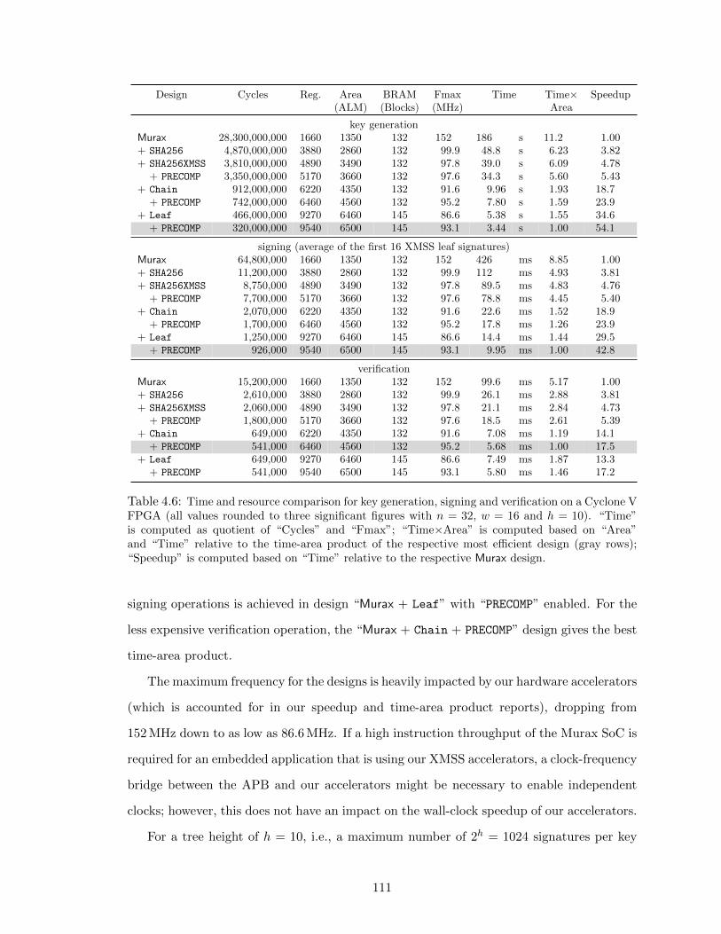
Design Cycles Reg. Area BRAM Fmax Time Time× Speedup(ALM) (Blocks) (MHz) Area
key generationMurax 28,300,000,000 1660 1350 132 152 186 s 11.2 1.00+ SHA256 4,870,000,000 3880 2860 132 99.9 48.8 s 6.23 3.82+ SHA256XMSS 3,810,000,000 4890 3490 132 97.8 39.0 s 6.09 4.78
+ PRECOMP 3,350,000,000 5170 3660 132 97.6 34.3 s 5.60 5.43+ Chain 912,000,000 6220 4350 132 91.6 9.96 s 1.93 18.7
+ PRECOMP 742,000,000 6460 4560 132 95.2 7.80 s 1.59 23.9+ Leaf 466,000,000 9270 6460 145 86.6 5.38 s 1.55 34.6
+ PRECOMP 320,000,000 9540 6500 145 93.1 3.44 s 1.00 54.1
signing (average of the first 16 XMSS leaf signatures)Murax 64,800,000 1660 1350 132 152 426 ms 8.85 1.00+ SHA256 11,200,000 3880 2860 132 99.9 112 ms 4.93 3.81+ SHA256XMSS 8,750,000 4890 3490 132 97.8 89.5 ms 4.83 4.76
+ PRECOMP 7,700,000 5170 3660 132 97.6 78.8 ms 4.45 5.40+ Chain 2,070,000 6220 4350 132 91.6 22.6 ms 1.52 18.9
+ PRECOMP 1,700,000 6460 4560 132 95.2 17.8 ms 1.26 23.9+ Leaf 1,250,000 9270 6460 145 86.6 14.4 ms 1.44 29.5
+ PRECOMP 926,000 9540 6500 145 93.1 9.95 ms 1.00 42.8
verificationMurax 15,200,000 1660 1350 132 152 99.6 ms 5.17 1.00+ SHA256 2,610,000 3880 2860 132 99.9 26.1 ms 2.88 3.81+ SHA256XMSS 2,060,000 4890 3490 132 97.8 21.1 ms 2.84 4.73
+ PRECOMP 1,800,000 5170 3660 132 97.6 18.5 ms 2.61 5.39+ Chain 649,000 6220 4350 132 91.6 7.08 ms 1.19 14.1
+ PRECOMP 541,000 6460 4560 132 95.2 5.68 ms 1.00 17.5+ Leaf 649,000 9270 6460 145 86.6 7.49 ms 1.87 13.3
+ PRECOMP 541,000 9540 6500 145 93.1 5.80 ms 1.46 17.2
Table 4.6: Time and resource comparison for key generation, signing and verification on a Cyclone VFPGA (all values rounded to three significant figures with n = 32, w = 16 and h = 10). “Time”is computed as quotient of “Cycles” and “Fmax”; “Time×Area” is computed based on “Area”and “Time” relative to the time-area product of the respective most efficient design (gray rows);“Speedup” is computed based on “Time” relative to the respective Murax design.
signing operations is achieved in design “Murax + Leaf” with “PRECOMP” enabled. For the
less expensive verification operation, the “Murax + Chain + PRECOMP” design gives the best
time-area product.
The maximum frequency for the designs is heavily impacted by our hardware accelerators
(which is accounted for in our speedup and time-area product reports), dropping from
152 MHz down to as low as 86.6 MHz. If a high instruction throughput of the Murax SoC is
required for an embedded application that is using our XMSS accelerators, a clock-frequency
bridge between the APB and our accelerators might be necessary to enable independent
clocks; however, this does not have an impact on the wall-clock speedup of our accelerators.
For a tree height of h = 10, i.e., a maximum number of 2h = 1024 signatures per key
111

pair, the time for XMSS key generation can be as short as only 3.44 s using our hardware
accelerators. Even more signatures per key pair are conceivably possible by use of multi-tree
XMSS, as shown in Table 4.7 (row “XMSSˆMTb”). By use of our hardware accelerators, we
can expect a similar speedup in accelerating XMSSˆMT as we achieved in XMSS. Signing
and verification computations are very efficient on our software-hardware co-design for all
the SHA-256 parameter sets, i.e., n = 32, w = 16, h = {10, 16, 20}: For h = 10, signing
takes only 9.95 ms and verification takes only 5.80 ms. For a bigger tree height, e.g., h =
20, signing and verification are only slightly more expensive: Signing takes 11.1 ms and
verification takes 6.25 ms, as shown in Table 4.7 (row “XMSSo with (n, h,w) = (32, 20, 16)”).
Our experiments show that running XMSS is very much feasible on a resource restricted
embedded device such as the Murax SoC with the help of efficient dedicated hardware
accelerators.
4.13 Comparison with Related Work
We first compare our work with a very recent work [103] which shows a similar software-
hardware co-design of XMSS. Then, we summarize all the existing FPGA-based implemen-
tations on other hash-based signature schemes. Finally, comparisons with implementations
of XMSS on other platforms are provided. Detailed comparison results are provided, as
shown in Table 4.7.
4.13.1 Software-Hardware Co-Design of XMSS
In 2019, Ghosh, Misoczki and Sastry [103] proposed a software-hardware co-design of XMSS
based on a 32-bit Intel Quark microcontroller and a Stratix IV FPGA. WOTS computations
are offloaded to a WOTS hardware engine which uses a general-purpose Keccak-400 hash
core as building block. In their design, generating one WOTS key pair takes 355,925 cycles,
consuming 2963 combinational logic cells and 2337 register cells. This hardware engine has
the same functionality as our WOTS module described in Section 4.9. In our design, the WOTS
module (with “+ PRECOMP”) takes 279,388 cycles for generating a key pair. The synthesis
result of our WOTS module on the same FPGA reports a usage of 2397 combinatorial logic
112
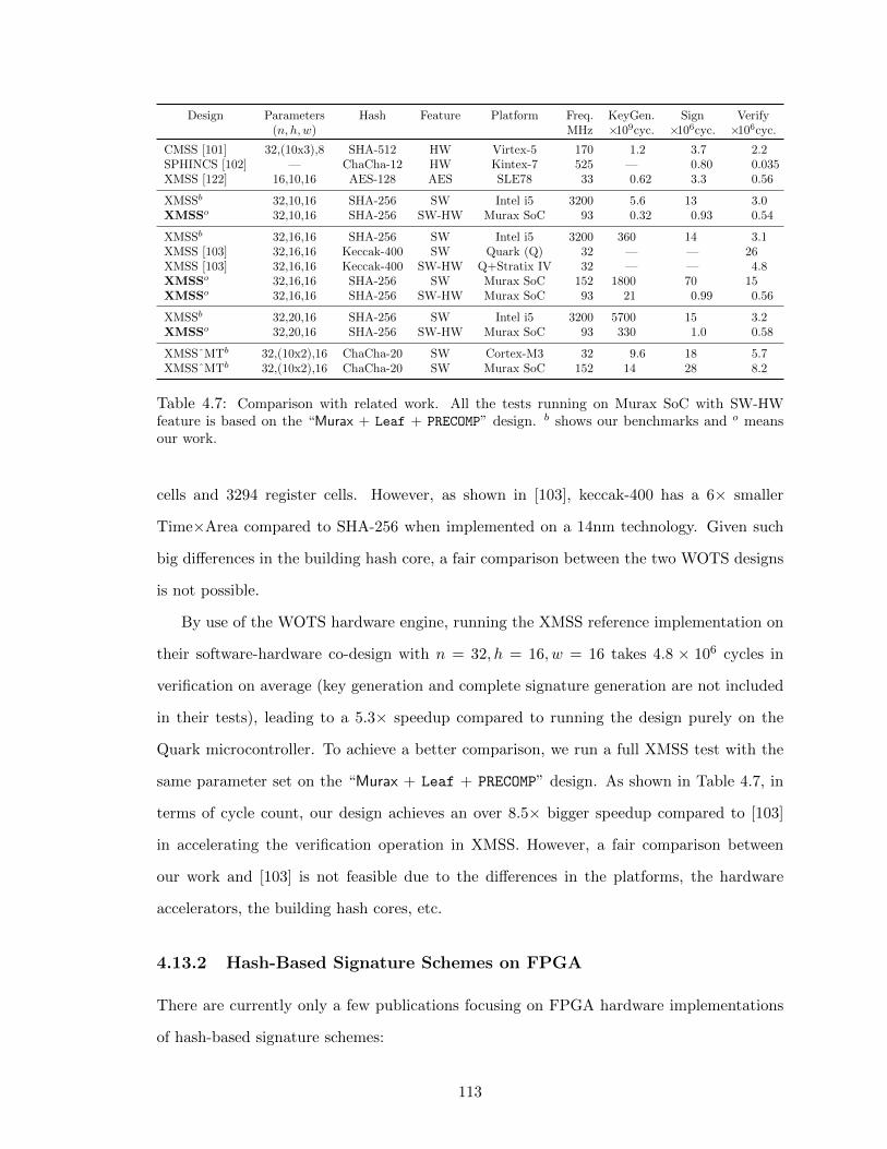
Design Parameters Hash Feature Platform Freq. KeyGen. Sign Verify(n, h,w) MHz ×109cyc. ×106cyc. ×106cyc.
CMSS [101] 32,(10x3),8 SHA-512 HW Virtex-5 170 1.2 3.7 2.2SPHINCS [102] — ChaCha-12 HW Kintex-7 525 — 0.80 0.035XMSS [122] 16,10,16 AES-128 AES SLE78 33 0.62 3.3 0.56
XMSSb 32,10,16 SHA-256 SW Intel i5 3200 5.6 13 3.0XMSSo 32,10,16 SHA-256 SW-HW Murax SoC 93 0.32 0.93 0.54
XMSSb 32,16,16 SHA-256 SW Intel i5 3200 360 14 3.1XMSS [103] 32,16,16 Keccak-400 SW Quark (Q) 32 — — 26XMSS [103] 32,16,16 Keccak-400 SW-HW Q+Stratix IV 32 — — 4.8XMSSo 32,16,16 SHA-256 SW Murax SoC 152 1800 70 15XMSSo 32,16,16 SHA-256 SW-HW Murax SoC 93 21 0.99 0.56
XMSSb 32,20,16 SHA-256 SW Intel i5 3200 5700 15 3.2XMSSo 32,20,16 SHA-256 SW-HW Murax SoC 93 330 1.0 0.58
XMSSˆMTb 32,(10x2),16 ChaCha-20 SW Cortex-M3 32 9.6 18 5.7XMSSˆMTb 32,(10x2),16 ChaCha-20 SW Murax SoC 152 14 28 8.2
Table 4.7: Comparison with related work. All the tests running on Murax SoC with SW-HWfeature is based on the “Murax + Leaf + PRECOMP” design. b shows our benchmarks and o meansour work.
cells and 3294 register cells. However, as shown in [103], keccak-400 has a 6× smaller
Time×Area compared to SHA-256 when implemented on a 14nm technology. Given such
big differences in the building hash core, a fair comparison between the two WOTS designs
is not possible.
By use of the WOTS hardware engine, running the XMSS reference implementation on
their software-hardware co-design with n = 32, h = 16, w = 16 takes 4.8 × 10⁶ cycles in
verification on average (key generation and complete signature generation are not included
in their tests), leading to a 5.3× speedup compared to running the design purely on the
Quark microcontroller. To achieve a better comparison, we run a full XMSS test with the
same parameter set on the “Murax + Leaf + PRECOMP” design. As shown in Table 4.7, in
terms of cycle count, our design achieves an over 8.5× bigger speedup compared to [103]
in accelerating the verification operation in XMSS. However, a fair comparison between
our work and [103] is not feasible due to the differences in the platforms, the hardware
accelerators, the building hash cores, etc.
4.13.2 Hash-Based Signature Schemes on FPGA
There are currently only a few publications focusing on FPGA hardware implementations
of hash-based signature schemes:
113

In 2011, Shoufan, Huber and Molter presented a cryptoprocessor architecture for the
chained Merkle signature scheme (CMSS) [101], which is a successor of the classic Merkle
signature scheme (MSS). All the operations, i.e., key generation, signing, and verification are
implemented on an FPGA platform. The performance of their design is shown in Table 4.7.
By use of these coprocessors, for parameters w = 8, tree height on a CMSS level h = 10 and
total CMSS levels T = 3, the authors report timings of 6.9 s for key generation, 21.5 ms for
signing and 13.2 ms for verification. In their design, twelve SHA-512 modules in total are
used to parallelize the design for better speedups.
Their implementation, however, is no longer state-of-the-art: They provide none of
the additional security features that have been developed for modern hash-based signature
schemes like XMSS, LMS [41], and the SPHINCS family [42]. The straightforward hash-
based operations are all replaced with more complex operations involving masks and keys
computed by pseudorandom functions. Therefore, direct comparisons between the hardware
modules among MSS and XMSS cannot be fairly done.
For modern hash-based signature schemes, an implementation of the stateless hash-based
signature scheme SPHINCS-256 [42] was proposed in [102] in 2018. This signature scheme
is closely related to XMSS and is a predecessor of the SPHINCS+ signature scheme [43],
which is one of the submissions in NIST’s PQC standardization process. SPHINCS-256
requires the cryptographic primitives BLAKE-256, BLAKE-512, and ChaCha-12. The au-
thors provide efficient hardware implementations for these primitives and control logic to
enable signing, key generation, and signature verification. They report timings of 1.53 ms
for signing and 65 µs for verification, but no timings for key generation.
The source code of all these works [101, 102] is not freely available. The detailed per-
formance data for the main hardware modules is not provided in the paper either. Lack of
access to the source code and detailed performance results make comparisons unfruitful.
4.13.3 XMSS on Other Platforms
We first benchmarked the original XMSS software implementation (linked against the
OpenSSL library) for all the SHA-256 parameter sets on an Intel i5-4570 CPU. The perfor-
mance results in Table 4.7 show that running the optimized XMSS software implementation
114

on our software-hardware co-design leads to an over 15× speedup in terms of clock cycles
compared to running the implementation on an off-the-shelf Intel i5 CPU. In 2012, Hulsing,
Busold, and Buchmann presented an XMSS-based implementation [122] on a 16-bit Infi-
neon SLE78 microcontroller, including key generation, signing and verification. The hash
functions are implemented by use of the embedded AES-128 co-processor. Performance
results for XMSS with n = 16, h = 10 and w = 16 maintaining a classical security level of
78-bit is provided. However, a fair comparison between our work and [122] is not feasible
since the security parameters used in [122] are already outdated.
The practicability of running SPHINCS [42] on a 32-bit ARM Cortex-M3 processor is
demonstrated in [117]. For comparison, they also implemented the multi-tree version of
XMSS (XMSSˆMT) on the same platform. Chacha-20 is used as the building hash function
in their design. To get a fair comparison between the performance of the Murax SoC and
a Cortex-M3 processor, we compiled a pure C-version of the code from [42] for both an
ARM Cortex-M3 processor and the Murax SoC and then measured the performance of
XMSSˆMT on these two platforms. As shown in Table 4.7, running the same test on the
Murax SoC gives a less than 50% slowdown in terms of cycle count compared to an off-
the-shelf ARM Cortex-M3 processor while the Murax SoC can run at an about 5× higher
clock frequency. This shows that the performance of the Murax SoC is comparable to the
Cortex-M3. Moreover, this test shows the feasibility of running the XMSSˆMT with a
bigger h = 20 on the Murax SoC.
4.14 XMSS Hardware Accelerators on ASIC
Over the last decade, active research has been focused on the software implementations and
FPGA designs of PQC schemes. However, today there is limited understanding on how
to implement these algorithms on an ASIC. There are only few publications that explore
ASIC designs of quantum-secure algorithms [123, 124]. To help expand understanding on
how to design ASIC accelerators for PQC algorithms, another line of our research on XMSS
focuses on developing efficient ASIC designs for the scheme.
In our work, we first implement the hardware design of a four stage-pipelined SHA-
115

256 accelerator, and demonstrate that the pipelined architecture improves the achievable
frequency of the SHA-256 core. Based on the pipelined SHA-256 core, we present the hard-
ware design of a pipelined XMSS Leaf accelerator, which achieves a much better frequency
compared to the existing non-pipelined XMSS Leaf accelerator. Both the non-pipelined
and the pipelined designs are then implemented on 28nm ASIC. By comparing the same
hardware designs on 28nm FPGAs and 28nm ASICs, we show that the XMSS Leaf accel-
erator is around an order of magnitude faster on the ASIC compared to an 28nm FPGA.
Further, the ASIC design design achieves a big power reduction: The ASIC consumes 10×
lower energy than the FPGA design for both the non-pipelined and the pipelined XMSS
Leaf accelerators. More details of our work on the ASIC designs of the XMSS scheme can
be found in [125].
4.15 Chapter Summary
In this chapter, we presented the first software-hardware co-design of XMSS on a RISC-V-
based embedded system. We first proposed two software optimizations targeting the most
frequently used SHA-256 function in XMSS. Based on the optimized XMSS software im-
plementation, we developed several hardware accelerators to speed up the most expensive
operations in XMSS, including a general-purpose SHA-256 accelerator, an XMSS-specific
SHA-256 accelerator, a WOTS-chain accelerator and an XMSS-leaf accelerator. The inte-
gration of these hardware accelerators to the RISC-V processor brings a significant speedup
in running XMSS on our software-hardware co-design compared to the pure software ver-
sion. Our work shows that embedded devices can remain future-proof by using algorithms
such as XMSS to ensure their security, even in the light of practical quantum computers.
116

Chapter 5
Lattice-based Cryptography:
Software-Hardware Co-Design of
qTESLA
This chapter presents a set of efficient and parameterized hardware accelerators that target
post-quantum lattice-based cryptographic schemes, including a versatile cSHAKE core, a
binary-search CDT-based Gaussian sampler, and a pipelined NTT-based polynomial multi-
plier, among others. Unlike much of prior work, the accelerators are fully open-sourced, are
designed to be constant-time, and can be parameterized at compile-time to support different
parameters without the need for re-writing the hardware implementation. These flexible,
publicly-available accelerators are leveraged to demonstrate the first software-hardware co-
design of the post-quantum lattice-based signature scheme qTESLA. The performance eval-
uation results on FPGAs successfully demonstrate the feasibility of running provably-secure
lattice-based schemes for embedded applications.
5.1 Background
Among the various post-quantum families, lattice-based cryptography [126, 127] repre-
sents one of the most promising and popular alternatives to today’s widely used public
key solutions. For instance, from the 9 NIST Round 2 digital signature candidates that
117

were selected, 3 belong to this cryptographic family: Dilithium [128], Falcon [129], and
qTESLA [130]. This chapter focuses on qTESLA, which is a signature scheme based on
the hardness of the ring learning with errors (R-LWE) problem that comes with built-in
defenses against some implementation attacks such as simple side-channel and fault attacks,
and against key substitution (KS) attacks [7]. Since instantiations of qTESLA are provably-
secure by construction, the signature scheme enjoys an important security guarantee: The
security hardness of a given instantiation is provably-guaranteed as long as its corresponding
R-LWE instance remains secure. This feature, however, comes at a price which is reflected
in the larger sizes, especially of public keys, and a slower performance.
5.1.1 Related Work
Due to the popularity of lattice-based schemes, there are many hardware designs in the
literature targeting the computing blocks that are necessary for the implementation of
lattice-based systems, such as the Gaussian sampler and the number theoretic transform
(NTT) [131, 132]. However, a recurrent issue is that most existing works, especially in the
case of the NTT, are not fully scalable or parameterized and are, hence, limited to specific
cryptographic schemes [131,133–135].
Banerjee et al. [123] proposed Sapphire, a configurable lattice crypto-processor closely
coupled with a customized RISC-V processor that has been tested on an ASIC using sev-
eral NIST candidates. Sapphire supports qTESLA, but their implementation correspond
to outdated parameters that are no longer part of the NIST PQC process. Another limita-
tion of this work is that, Banerjee et al.’s Gaussian sampler is based on a merge-sort CDT
algorithm that employs full-scan search for software implementations. The full-scan search
approach, despite being able to eliminate timing and cache attacks in software implemen-
tations, has been shown to be much more expensive when being mapped to hardware [136],
compared to hardware designs of Gaussian samplers based on other search algorithms [132].
Farahmand et al. [137] proposed a software-hardware co-design architecture to bench-
mark various lattice-based KEMs. To speed up the design process they use the popular
Zynq UltraScale+ SoC which contains hard ARM processor cores coupled to the FPGA
fabric. Thus, they benefit from the high clock frequencies of the ARM processor built into
118

the FPGA. However, their work only supports designs with modulus q being a power-of-
two or NTRU-based KEMs [138]. Hence, their arithmetic blocks do not support any of
the Round 2 nor Round 3 lattice-based digital signature candidate proposals. Furthermore,
they only include a simple schoolbook multiplier.
5.1.2 Motivation for Our Work
Post-quantum cryptography (PQC), including lattice-based cryptography, is still an active
research area and, as a consequence, there is a proliferation of schemes and a rapid evolution
in the parameters that are used in practical instantiations, as can be observed in the ongoing
NIST PQC standardization process. This issue is markedly problematic and expensive for
hardware. Hence, unlike much of prior work, the accelerators developed in this work are
designed to be fully parameterized at compile-time to help implement different parameters
and support different lattice-based schemes. These flexible accelerators are then used to
realize the first RISC-V based software-hardware co-design of qTESLA with the provably-
secure parameter sets. This successfully demonstrates the significant impact of offloading
complex functions from software to hardware accelerators. The modules are fully parame-
terized and, hence, allow us to quickly change parameters and re-synthesize the design. For
example, in our design, it is made easy to switch from qTESLA’s Round 2 provably-secure
parameters to prior heuristic parameters, if desired. Finally, a relevant feature of our design
is the use of a simple and standard 32-bit interconnect to the microcontroller. This design
feature aims at providing platform flexibility and showing that hardware accelerators can
achieve good performance even with this conservative choice.
This chapter is based on our publication [8]. The contributions and organizations of
this chapter are as follows:
• We give an introduction in Section 5.2 to the qTESLA signature scheme.
• We show the basic software implementation for qTESLA and present the software pro-
filing results that determine potential functions for promising speedups using hardware
acceleration in Section 5.3.
• We develop several hardware accelerators to speed up the most expensive operations
119

in qTESLA, which were selected based on the software profiling results. These accel-
erators include a unified and scalable SHAKE accelerator that can be easily configured
as SHAKE or cSHAKE of 128-bit or 256-bit security level (described in Section 5.4),
a novel and lightweight CDT-based Gaussian sampler (described in Section 5.5), a
fully parameterized and pipelined NTT-based polynomial multiplier (described in Sec-
tion 5.6), a parameterized sparse polynomial multiplier (described in Section 5.7) and
a lightweight Hmax-Sum module (described in Section 5.8). These hardware acceler-
ators achieve a significant speedup compared to running the corresponding functions
in the qTESLA reference implementation in software.
• In Section 5.9, we give a high-level view of the SoC platform we used to develop the
hardware architecture, and show how to integrate customized hardware accelerators
into the SoC.
• In the end, we present the hardware prototype of the software-hardware co-design of
qTESLA on a RISC-V embedded processor in Section 5.10.
• The evaluation results in Section 5.11 and comparison results with related work in
Section 5.12 successfully demonstrate the practicability and efficiency of running the
provably-secure qTESLA signature scheme on embedded systems.
• In the end, a short summary for this chapter is given in Section 5.13.
5.2 The qTESLA Scheme
qTESLA is a provably-secure post-quantum signature scheme, based on the hardness of the
decisional R-LWE problem [130]. The scheme is based on the “Fiat-Shamir with Aborts”
framework by Lyubashevsky [139] and is an efficient variant of the Bai-Galbraith signature
scheme [140] adapted to the setting of ideal lattices. A distinctive feature of qTESLA is
that its parameters are provably secure, i.e., they are generated according to the security
reduction from R-LWE.
Notation. We define the rings R = Z[x]/〈xn + 1〉 and Rq = Zq[x]/〈xn + 1〉, where n is
the dimension and Zq = Z/qZ for a prime modulus q ≡ 1 mod 2n. We further define the
120

sets Hn,h = {∑n−1
i=0 fixi ∈ R | fi ∈ {−1, 0, 1},
∑n−1i=0 |fi| = h} and Rq,[B] = {
∑n−1i=0 fix
i ∈
R | fi ∈ [−B,B]} for fixed system parameters h and B. For some even (odd) modulus m ∈
Z≥0 and an element c ∈ Z, c′ = c mod±m denotes the unique element −m/2 < c′ ≤ m/2
(resp., −bm/2c ≤ c′ ≤ bm/2c) with c′ = c mod m. We also define the rounding functions
[·]L : Z → Z, c 7→ (c mod±q) mod±2d, and [·]M : Z→ Z, c 7→ (c mod±q − [c]L)/2d for a
fixed system parameter d. These definitions are extended to polynomials by applying the
operators to each polynomial coefficient, i.e., [f ]L =∑n−1
i=0 [fi]L xi and [f ]M =
∑n−1i=0 [fi]M xi
for a given f =∑n−1
i=0 fixi ∈ R. Given f ∈ R, we define the function maxi(f) which returns
the i-th largest absolute coefficient of f . For an element c ∈ Z, we have that ‖c‖∞ =
|c mod±q|, and define the infinity norm for a polynomial f ∈ R as ‖f ‖∞ = maxi‖fi‖∞.
To denote sampling each coefficient of a polynomial f with centered discrete Gaussian
distribution Dσ with standard deviation σ, we write f ←σ R.
Besides the number of polynomial coefficients n and the modulus q, the R-LWE setup
also involves defining the number of R-LWE samples that are used by the scheme instantia-
tion, which we denote by k. The values E and S define the coefficient bounds for the error
and secret polynomials, B determines the interval from which the random coefficients of the
polynomial y are chosen during signing, and bGenA ∈ Z>0 represents the number of blocks
requested in the first cSHAKE call during generation of the so-called public polynomials
a1, . . . , ak [130]. Finally, we define two additional system parameters: λ, which denotes the
targeted bit-security of a given instantiation, and κ, which denotes the input and output
bit length of the hash and pseudo-random functions (PRFs).
qTESLA is parameterized by λ, κ, n, k, q, σ, E, S, B, d, h, and bGenA, discussed above.
The pseudo-code of qTESLA’s key generation, sign and verify algorithms are presented in
Algorithms 7, 8 and 9, respectively. A brief description of the algorithms, highlighting the
most important operations of the scheme, follows. For complete information and details
about the different qTESLA functions, readers are referred to [130].
5.2.1 Key Generation
Gaussian sampling is used to generate the secret and error polynomials in R with centered
discrete Gaussian distribution Dσ. The polynomials produced by the Gaussian sampler
121

Algorithm 7 qTESLA’s key generation [130]
Require: -Ensure: sk = (s, e1, . . . , ek, sa, sy, g) and pk =
(t1, . . . , tk, sa)
1: counter← 12: seed←$ {0, 1}κ3: ss, se1 , . . . , sek , sa, sy ← PRF1(seed)4: a1, . . . , ak ← GenA(sa)5: do6: s← GaussSampler(ss, counter)7: counter← counter + 18: while checkS(s) 6= 09: for i = 1, . . . , k do
10: do11: ei ← GaussSampler(sei , counter)12: counter← counter + 113: while checkE(ei) 6= 014: ti ← ais+ ei mod q
15: g ← G(t1, . . . , tk)16: sk ← (s, e1, . . . , ek, sa, sy, g)17: pk ← (t1, . . . , tk, sa)18: return sk, pk
(denoted by GaussSampler) have to pass two security checks, namely, checkE and checkS,
which make sure that∑h
i=1 maxi(f) (called Hmax-Sum in the remainder) is less than or
equal to the fixed bounds E and S, respectively. For the generation of the public keys, we
need to derive the public polynomials a1, . . . , ak ∈ Rq. This operation is denoted by the
function GenA : {0, 1}κ → Rkq . The random seed sa that is used to generate the public
polynomials is transmitted to the signing and verification algorithms through the secret
and public keys, respectively. We highlight that the fresh generation of a1, . . . , ak using
a random seed saves bandwidth, makes the introduction of backdoors more difficult and
minimizes the impact of all-for-the-price-of-one attacks [130]. We also point out that the
secret key includes a value denoted by g, which is the hash of the polynomials t1, . . . , tk
(which are part of the public key), computed via the function G : {0, 1}∗ → {0, 1}320 [7].
This is then used during the hashing operation to derive the challenge value c′ at signing.
This design feature protects against key substitution attacks [141], by guaranteeing that
any attempt by an attacker of modifying the public key will be detected during verification
when checking c′.
122

Algorithm 8 qTESLA’s signature generation [130]
Require: m, sk = (s, e1, . . . , ek, sa, sy, g)Ensure: (z, c′)
1: counter← 12: r ←$ {0, 1}κ3: rand← PRF2(sy, r,G(m))4: y ← ySampler(rand, counter)5: a1, . . . , ak ← GenA(sa)6: for i = 1, . . . , k do7: vi = aiy mod±q
8: c′ ← H(v1, . . . , vk,G(m), g)9: c , {pos list, sign list} ← Enc(c′)
10: z ← y + sc11: if z /∈ Rq,[B−S] then12: counter← counter + 113: Restart at step 4
14: for i = 1, . . . , k do15: wi ← vi − eic mod±q16: if ‖[wi]L‖∞ ≥ 2d−1 − E ∨ ‖wi‖∞ ≥ bq/2c − E then17: counter← counter + 118: Restart at step 4
19: return (z, c′)
Algorithm 9 qTESLA’s signature verification [130]
Require: m, (z, c′), pk = (t1, . . . , tk, sa)Ensure: {0,−1} . accept, reject signature
1: c , {pos list, sign list} ← Enc(c′)2: a1, . . . , ak ← GenA(sa)3: for i = 1, . . . , k do4: wi ← aiz − tic mod±q
5: if z /∈ Rq,[B−S] ∨ c′ 6= H(w1, . . . , wk,G(m),G(t1, . . . , tk)) then6: return −1
7: return 0
5.2.2 Signature Generation and Verification
During signing, the sampling function ySampler samples a polynomial y ∈ Rq,[B]. To pro-
duce the randomness rand used to generate y, one uses a secret-key value sy and some fresh
randomness r. The use of sy makes qTESLA resilient to fixed-randomness attacks such
as the one demonstrated against Sony’s Playstation 3 [142], and the random value r guar-
antees the use of a fresh y at each signing operation, which makes qTESLA’s signatures
probabilistic and, hence, more difficult to attack through side-channel analysis. In addition,
the fresh y protects against some powerful fault attacks against deterministic signature
schemes [143,144]. Signing and verification also require the generation of the challenge c′ by
123

λ κ n k q σ h E = S B d bGenAqTESLA-p-I 95 256 1024 4 343, 576, 577 8.5 25 554 219 − 1 22 108qTESLA-p-III 160 256 2048 5 856, 145, 921 8.5 40 901 221 − 1 24 180
Table 5.1: Parameters of the two qTESLA parameter sets (from Round 2 submission [130]).
using the hash-based function H, which computes [v1]M , . . . , [vk]M for some polynomials vi
(or wi during verification) and hashes these together with the digests G(m) and G(t1, ..., tk).
This value is then mapped deterministically (using the function Enc) to a pseudo-randomly
generated polynomial c ∈ Hn,h which is encoded as the two arrays pos list ∈ {0, . . . , n−1}h
and sign list ∈ {−1, 1}h representing the positions and signs of the nonzero coefficients of
c, respectively. At signing, in order for the potential signature (z ← sc+y, c′) to be returned
by the signing algorithm, it needs to pass a security check, which verifies that z /∈ Rq,[B−S],
and a correctness check, which verifies that ‖[wi]L‖∞ < 2d−1−E and ‖wi‖∞ < bq/2c −E.
At verification, if for a given signature (z, c′) it holds that z ∈ Rq,[B−S] and c′ matches
the value computed using the function H as described above, the signature is accepted;
otherwise, it is rejected.
Hashing and pseudo-random generation are required by several computations in the
scheme. This functionality is provided by the extendable output functions SHAKE [145],
in the realization of the functions G and H, and cSHAKE [146], in the realization of the
functions PRF1, PRF2, ySampler, GaussSampler, GenA and Enc. Although implementers are
free to pick a cryptographic PRF of their choice to implement PRF1, PRF2, ySampler, and
GaussSampler, we chose to reuse the same (c)SHAKE core to also support these functions
in order to save area. According to the specifications [130], the use of cSHAKE-128 is fixed
for GenA and Enc. For the remaining functions, level 1 and level 3 parameter sets use
(c)SHAKE-128 and (c)SHAKE-256, respectively.
5.2.3 Security Parameters
qTESLA’s NIST PQC submission for Round 2 includes two parameter sets: qTESLA-p-I
and qTESLA-p-III, which target NIST security levels 1 and 3, respectively, and are assumed
to provide post-quantum security equivalent to AES-128 and AES-192, respectively [147].
We show the instantiations with their relevant parameters in Table 5.1. The parameters
124

for qTESLA-p-I lead to a signature, public key and secret key of 2, 592 bytes, 14, 880 bytes
and 5, 224 bytes, respectively. The corresponding figures for qTESLA-p-III are 5, 664 bytes,
38, 432 bytes and 12, 392 bytes, respectively [1].
5.3 Reference Software Implementation and Profiling
This section provides background on software profiling used to identify most suitable func-
tions for hardware acceleration, and gives details about these functions.
5.3.1 Basis Software Implementation
In our design, we used qTESLA’s most recent portable C reference implementation that
was submitted to the NIST PQC standardization process (Round 2) as the basis software
implementation1. It is a state-of-the-art 32/64-bit software implementation of qTESLA,
targeting a low clock cycle count. This is the fastest reference software implementation of
qTESLA we are aware of. We chose the definitions of the targeted architecture and basic
data types to ensure that the code runs correctly on 32-bit architectures (i.e., on our RISC-
V target) and we used the available compiler flags to enable the highest optimization levels
of the GCC compiler.
5.3.2 Software Profiling
To determine potential functions for promising speedups using hardware acceleration, we
profiled qTESLA’s reference software implementation. We profiled the code with gprof on a
3.4GHz Intel Core i7-6700 (Skylake) CPU with TurboBoost disabled. As a result, we found
that the two most expensive operations are (c)SHAKE and the NTT-based polynomial
multiplication: About 39.4% of the computing time is spent by the Keccak function
performing cSHAKE and SHAKE computations, and about 27.9% of the time is spent by
the polynomial multiplier performing NTT computations. Other costly operations include
the sparse polynomial multiplications (6.3% of the total cost) and the Gaussian sampler
(4.5% of the total cost). Accordingly, these four functions were selected for hardware
1. The software is available at https://github.com/qtesla/qTesla, commit-id d8fd7a5.
125

acceleration. Interestingly, after acceleration, we discovered that the Hmax-Sum function
became a new bottleneck, and it was accelerated as well. This highlights the importance
of repeated profiling in order to reassess the performance of functions that are originally
considered inexpensive.
5.3.3 Functions Selected for Hardware Acceleration
Based on the profiling results in Section 5.3.2, we designed accelerators for (c)SHAKE, NTT-
based polynomial multiplier, Gaussian sampler, sparse multiplication and Hmax-Sum. The
first 3 of these functions are also targeted because they are commonly found in lattice-based
cryptography and can be used to accelerate other cryptographic schemes.
(c)SHAKE. SHAKE [145] and cSHAKE [146] are extendable output functions (XOF)
based on the Keccak algorithm [148,149], which is also the basis of NIST’s SHA-3 standard
[145]. XOFs are similar to hash functions, but while hash functions only produce a fixed
length output, XOFs produce a variable amount of output bits.
Keccak is a parameterizable sponge function, where b denotes the state size, r the
rate, and c the capacity and b = r + c. For current NIST algorithms based on Keccak,
the state is set to b = 25 × 26 = 1600, while c (and r) vary. Therefore, NIST’s algorithms
are usually described in the form Keccak[c](message, outputlength). For SHAKE128 and
cSHAKE128, c = 128 and for the other two variants c = 256. Based on Keccak, they can
be defined as:
SHAKE-c(M,d) =Keccak[c](M ||1111, d)
cSHAKE-c(M,N,S, d) =Keccak[c](bytepad(encode string(N)||
encode string(S), c/8)||M ||00, d).
N is a so-called function-name string, defined by NIST, and S a customization bit string.
It is further defined that, if N and S are empty strings, cSHAKE = SHAKE. Sponge
functions such as Keccak have an absorption and a squeezing phase. In the absorption
phase r bits are combined with the internal state using XOR, followed by a computation of
126
the internal Keccak permutation. Hence, if n bits have to be absorbed, dnr e absorptions
have to be performed. Similarly, in the squeezing phase r bits of output are produced,
followed by one or more executions of the Keccak permutation, if more than r bits are
requested. Due to this general design, it is possible to use the same implementation of the
internal permutation for all needed SHAKE and cSHAKE implementations, if the inputs
are properly prepared and padded.
Polynomial Multiplication. Setting q ≡ 1 mod 2n enables the use of the efficient NTT
for polynomial multiplication, which we define next.
Let ω and φ be primitive n-th and 2n-th roots of unity in Zq, respectively, where φ2 = ω.
Then, for a polynomial c =∑n−1
i=0 cixi the forward NTT transform is defined as
NTT : R = Zq[x]/〈xn + 1〉 → Rq, c 7→ c =
n−1∑i=0
n−1∑j=0
cjφjωij
xi.
Likewise, the inverse NTT transform is defined as
NTT−1 : Rq → R = Zq[x]/〈xn + 1〉, c 7→ c =n−1∑i=0
n−1φ−i n−1∑j=0
cjω−ij
xi.
In qTESLA, the NTT is used to carry out the polynomial multiplications in line 7 of
Algorithm 8 and in line 4 of Algorithm 9. In particular, given that public polynomials
a1, . . . , ak are assumed to be generated directly in the NTT domain, multiplications have
the form ai · b in Rq, for some b ∈ Rq, and can be computed as NTT−1(ai ◦NTT(b)), where
◦ is the coefficient-wise multiplication.
Sparse Polynomial Multiplication. In addition to standard polynomial multiplications
which are dealt with the NTT, qTESLA also performs polynomial multiplications with the
sparse polynomial c ∈ Hn,h, in lines 10 and 15 of Algorithm 8 and in line 4 of Algorithm 9.
Recall that c is encoded as two lists pos list and sign list ∈ {−1, 0, 1}h which represent
the positions and signs of its nonzero coefficients, respectively. These multiplications can
be specialized with an algorithm that exploits the sparseness; see [7, Alg. 11].
Discrete Gaussian Sampler. Discrete Gaussian samplers are parameterized by the pre-
127

Parameter setCDT parameters
targeted precision implemented precision number of rows table sizeβ (bits) t (bytes)
qTESLA-p-I 64 63: 78 624qTESLA-p-III 128 125 111 1776
Table 5.2: CDT parameters used in qTESLA’s Round 2 implementation.
cision of the samples (which we denote by β), the standard deviation σ of the Gaussian
distribution, and the tail-cut τ , such that the range of the samples is [−στ, στ ] ∩ Z. There
are several sampling techniques, such as rejection [150], Bernoulli [151], Ziggurat [152],
CDT [153], and Knuth-Yao [154]. Among them, the cumulative distribution table (CDT) of
the normal distribution [153] is one of the most efficient methods when σ is relatively small,
as is the case in, e.g., the R-LWE encryption schemes by Lyubashevsky et al. [155] and by
Linder and Peikert [156] and the NIST PQC candidates FrodoKEM [157] and qTESLA [130].
In addition, this method is also easy to implement securely in constant-time and avoids the
need for floating point operations, which are especially expensive in hardware.
The method consists of pre-computing a table CDT[i] := b2β Pr[c 6 i | c ←σ Z]c for
i ∈ [0, . . . , t − 1] offline, using the smallest t such that Pr[|c| > t | c ←σ Z] < 2−β. Then,
during the online computation one picks a uniform sample u ←$ Z/2βZ generated by a
PRNG, scans the table, and finally returns the value s such that CDT[s] 6 u < CDT[s + 1].
To cover the full sampling range, a random bit is used to assign the sign to the Gaussian
sample s. Table 5.2 includes the specific CDT parameters used in qTESLA implementations.
Hmax-Sum. In qTESLA, after sampling a secret polynomial ei or s during key generation,
the polynomial has to be checked to see if the sum of its largest h coefficients is smaller
than a pre-defined bound E or S. If the sum is smaller than the bound, then the sampled
polynomial is accepted as valid. Otherwise, it is rejected and the procedure is repeated
again. We denote this procedure as the Hmax-Sum function.
In the following sections, we describe the details of the proposed hardware modules.
128
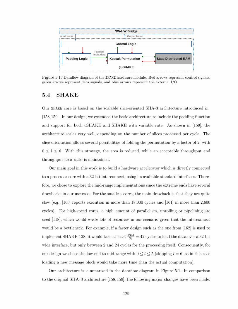
SW-HW Bridge
Control Logic
Padding Logic Keccak Permutation State Distributed RAM
(c)SHAKE
Padded input data
Input frame
Output frame
Figure 5.1: Dataflow diagram of the SHAKE hardware module. Red arrows represent control signals,green arrows represent data signals, and blue arrows represent the external I/O.
5.4 SHAKE
Our SHAKE core is based on the scalable slice-oriented SHA-3 architecture introduced in
[158,159]. In our design, we extended the basic architecture to include the padding function
and support for both cSHAKE and SHAKE with variable rate. As shown in [159], the
architecture scales very well, depending on the number of slices processed per cycle. The
slice-orientation allows several possibilities of folding the permutation by a factor of 2l with
0 ≤ l ≤ 6. With this strategy, the area is reduced, while an acceptable throughput and
throughput-area ratio is maintained.
Our main goal in this work is to build a hardware accelerator which is directly connected
to a processor core with a 32-bit interconnect, using its available standard interfaces. There-
fore, we chose to explore the mid-range implementations since the extreme ends have several
drawbacks in our use case. For the smallest cores, the main drawback is that they are quite
slow (e.g., [160] reports execution in more than 18,000 cycles and [161] in more than 2,600
cycles). For high-speed cores, a high amount of parallelism, unrolling or pipelining are
used [118], which would waste lots of resources in our scenario given that the interconnect
would be a bottleneck. For example, if a faster design such as the one from [162] is used to
implement SHAKE-128, it would take at least 134432 = 42 cycles to load the data over a 32-bit
wide interface, but only between 2 and 24 cycles for the processing itself. Consequently, for
our design we chose the low-end to mid-range with 0 ≤ l ≤ 5 (skipping l = 6, as in this case
loading a new message block would take more time than the actual computation).
Our architecture is summarized in the dataflow diagram in Figure 5.1. In comparison
to the original SHA-3 architecture [158,159], the following major changes have been made:
129

• Support for cSHAKE and SHAKE, instead of SHA-3.
• Support for both 128-bit and 256-bit parameter sets.
• Direct integration of the padding functionality into the core.
5.4.1 Communication Protocol
The processor communicates with our core using a new protocol with several different 32-bit
frames for data transmission:
• A command frame to distinguish between the four different operation modes cSHAKE-
128, cSHAKE-256, SHAKE-128, and SHAKE-256. This command frame also specifies
the output length generated by the SHAKE core.
• A customization frame to transfer the cSHAKE customization string to the core. Our
implementation follows the cSHAKE-simple strategy and supports a 16-bit customiza-
tion string [163].
• A length frame, which specifies the length of the input data block. This length infor-
mation has to be either equal to the rate of the selected function, or less. If the block
to be transferred is the last message block to be absorbed, an additional end flag in
this length frame is set.
• A message frame that contains the message block to be absorbed. For a message block
of length m ≤ r, dm32e frames have to be transmitted.
The interface uses a handshake mechanism borrowed from AXI4-Lite [164] to implement
the data transfer.
5.4.2 Hardware Implementation
Control Logic. The control logic uses the input frames to control the padding logic, the
permutation, and indirectly the distributed RAM used as state memory. If the core is idle
and a command frame is received, the control logic switches to the appropriate internal state
and expects as the next frame either the customization frame, if cSHAKE is requested, or
the length frame. The rate r for the relevant variant and the requested output length d
130

are stored internally. The rate r and the information, if SHAKE or cSHAKE has to be
performed, is later used to calculate the number of bits to absorb per message block and
the number of bits to squeeze. The information also controls the different encodings of the
customization string and the padding (since SHAKE and cSHAKE use slightly different
padding schemes).
If cSHAKE is requested, a customization frame is processed next. The necessary ab-
sorption phase for the customization string is faster than absorbing a full message block.
According to the cSHAKE encoding rules, the total length to be absorbed is only 64 bits for
a 16-bit customization string. Therefore, it is possible to absorb the customization string
in only 642l
cycles, independently of the actual rate, plus the time to execute the Keccak
permutation once. After absorbing the string, the length frame is expected. A length frame
describes how many message frames have to be transmitted to the SHAKE core and also if it
is the last message block. Each message frame is directly absorbed, needing r2l
cycles per
block, depending on the configuration of the core. If the last message frame is received,
the SHAKE or cSHAKE padding is applied. Afterwards, the core automatically starts to
squeeze out the requested amount of output data and sends it back to the processor. Each
step in the squeezing phase consists of transferring r bits over the communication link,
followed by one computation of the Keccak permutation, if more bits need to be squeezed.
Sending data back to the processor is much simpler, as it is only necessary to transfer the
data in 32-bit output frames over the interface without any additional protocol overhead.
Padding Logic. The padding needs to fill up a message block to a multiple of the rate r.
Since our core supports bit-wise input lengths, this leads to 25×2l multiplexers, depending
on the number of slices processed in parallel. These multiplexers switch between the input
data, ‘0’ and ‘1’, depending on the length of the message to be absorbed. Beside the length
of the message block, the output of the multiplexer also depends on the selected operation
mode of the SHAKE core, because the padding differs between SHAKE and cSHAKE func-
tions. Additionally, if the padding does not fit into the message block, an extra message
block needs to be absorbed.
Permutation. The implementation of the permutation follows the original slice-oriented
131

Design Features Platform Slices/LUTs/FFs TP/Area Fmax(Func./Pad./Standard IO) (MBit/s/slice) (MHz)
p=1 (c)SHAKE-128/256, X, X Artix-7 249/811/490 0.29 178p=2 (c)SHAKE-128/256, X, X Artix-7 273/908/450 0.48 163p=4 (c)SHAKE-128/256, X, X Artix-7 312/1069/361 0.81 158p=8 (c)SHAKE-128/256, X, X Artix-7 404/1466/270 1.31 164p=16 (c)SHAKE-128/256, X, X Artix-7 657/2401/226 1.62 165p=32 (c)SHAKE-128/256, X, X Artix-7 1149/4436/180 1.79 161
p=1 [165] SHA-3-256, —, X Artix-7 172/—/— 0.42 179p=2 [165] SHA-3-256, —, X Artix-7 207/—/— 0.62 159p=4 [165] SHA-3-256, —, X Artix-7 247/—/— 1.19 179p=8 [165] SHA-3-256, —, X Artix-7 293/—/— 1.61 145p=8 [165] SHA-3-256, X, X Artix-7 482/—/— 2.03 180p=16 [165] SHA-3-256, —, X Artix-7 463/—/— 2.1 150p=32 [165] SHA-3-256, —, X Artix-7 900/—/— 1.99 138[166] SHA-3-256, —, — Virtex-6 49/193/41 0.22 198[166] SHA-3-256, —, — Virtex-6 60/174/71 0.42 426[162] SHA-3-256, —, — Virtex-6 1432/—/— 10.33 327
Table 5.3: Performance of the proposed SHAKE hardware module and comparison with state-of-the-art related work.
design from [159]. In summary, the implementation uses the following ideas. Firstly, if 2l
slices are processed in parallel in each cycle, only a smaller part of the total Keccak permu-
tation – namely, 2l
64 of the combinational logic – must be implemented, but then reiterated
for 642l
cycles for a complete round. The required combinational logic is implemented in the
permutation module, while the required bit-shuffling is implemented using an addressing
scheme in the state RAM module.
One important complicating factor for the implementation is data dependencies between
consecutive slices. These dependencies require that the permutation keep some internal
state between consecutive clock cycles, and also between two consecutive rounds, which
adds some overhead to the otherwise straightforward implementation of the combinational
logic part.
5.4.3 Evaluation and Related Work
Table 5.3 shows the evaluation results for our SHAKE core and some state-of-the-art results
from the literature. The approximate number of clock cycles for SHAKE and cSHAKE is
132

calculated as follows:
cyclesSHAKE = 1 + dm1
re(1 +
r + 1600
2l) + dm2
re(r + 1600
2l)− 1600
2l
cyclescSHAKE =64 + 1600
2l+ cyclesSHAKE
where m1 is the length of the message to be absorbed, r is the rate, p = 2l is the number
of slices processed in parallel, and m2 is the output length. Both m1 and m2 are given in
bits. The number is only approximated, since it assumes that no extra message block for
the padding is needed.
For the purpose of comparing the throughput with previous works on SHA-3, we as-
sume that long messages are processed and only a short output with m2 < r is requested.
Also, Table 5.3 only includes results corresponding to SHA-3-256’s rate. As expected, the
area consumption of our core goes up compared to the implementation reported in [165].
However, the general trend is very similar, with an offset between 70 and 249 slices, which
is due to the increased feature set, i.e., the original core does not implement any padding
functionality, and only includes one fixed hash function, namely SHA-3-256.
As expected, our design cannot compete with the smallest design from [166], nor with
the high-throughput core from [162] in their respective benchmark categories. However, as
mentioned earlier, both design targets would lead to a sub-optimal performance in our use
case with a standard 32-bit interface, because either the processing time of a low-end core
would not provide sufficient speed or a high-speed core would waste resources since it would
spend most of the time waiting for new input. Overall, we can see that an extended feature
set of a Keccak core can be implemented with a reasonable overhead.
Applicability to Other Cryptographic Schemes. SHAKE and cSHAKE are versatile
cryptographic primitives with broad applications in cryptographic protocols. Importantly,
similar to our qTESLA’s profiling results in Section 5.3.2, SHAKE and cSHAKE have been
found to be responsible for significant portions of the computing cost of several of the
post-quantum schemes in the NIST PQC process, including FrodoKEM [157], Saber [167],
NewHope [168], Kyber [169], and others. Thus, our SHAKE core offers a flexible and efficient
architecture with different area and performance trade-offs that can be easily used to accel-
133

erate the hash and XOF computations of (post-quantum) schemes for different applications.
5.5 Gaussian Sampler
As discussed in Section 5.3.3, we chose a CDT-based Gaussian sampler for our design due
to its simplicity and efficiency in hardware when the standard deviation σ is relatively
small. This sampler can be implemented with different search algorithms, such as full-
scan search, binary search, and others. Since binary search does not run in constant-time
on general-purpose computers due to the presence of cache memory, qTESLA’s software
implementation [7] employs full-scan search to prevent timing and cache attacks. However,
for hardware implementations, by exploiting the fact that the memory access time is fixed
and constant, we can speed up the CDT-based Gaussian sampler by use of binary search.
5.5.1 Algorithm
We present our novel time-invariant CDT-based Gaussian sampling algorithm using binary
search in Algorithm 10. In the algorithm, CDT is a pre-computed table intended to be saved
into a memory block in hardware, the input to the Gaussian sampler is a random number
x of precision β generated by a PRNG, and the output is a signed Gaussian sample s of
width dlog2(t)e + 1, where t is the depth of CDT; see Table 5.2. The sign is determined by
the most significant bit of x. The basic idea of the algorithm is to use the CDT table to
fix two overlapping “power-of-two” sub-tables with the same size 2dlog2(t)e−1, and then run
a binary search in which the first, lower-address sub-table is given priority. For example,
for t = 624 the CDT table is split into the sub-tables of ranges [0, 511] and [112, 623]. The
former table is given priority and, hence, inputs falling in the overlapping range execute
binary search on it. Since memory access time is constant in our setting and the sampler
runs the same number of iterations for all possible inputs, the algorithm is protected against
timing attacks.
134
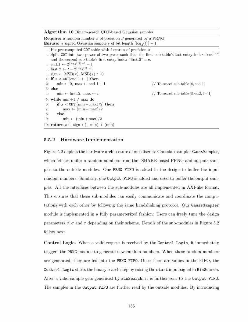
Algorithm 10 Binary-search CDT-based Gaussian sampler
Require: a random number x of precision β generated by a PRNG.Ensure: a signed Gaussian sample s of bit length dlog2(t)e+ 1.
. Fix pre-computed CDT table with t entries of precision β.
. Split CDT into two power-of-two parts such that the first sub-table’s last entry index “end 1”and the second sub-table’s first entry index “first 2” are:
. end 1 ← 2dlog2(t)e−1 − 1
. first 2 ← t− 2dlog2(t)e−1
. sign ← MSB(x), MSB(x)← 01: if x < CDT[end 1 + 1] then2: min← 0, max← end 1 + 1 // To search sub-table [0, end 1]
3: else4: min← first 2, max← t // To search sub-table [first 2, t− 1]
5: while min +1 6= max do6: if x < CDT[(min + max)/2] then7: max← (min + max)/28: else9: min← (min + max)/2
10: return s← sign ? (−min) : (min)
5.5.2 Hardware Implementation
Figure 5.2 depicts the hardware architecture of our discrete Gaussian sampler GaussSampler,
which fetches uniform random numbers from the cSHAKE-based PRNG and outputs sam-
ples to the outside modules. One PRNG FIFO is added in the design to buffer the input
random numbers. Similarly, one Output FIFO is added and used to buffer the output sam-
ples. All the interfaces between the sub-modules are all implemented in AXI-like format.
This ensures that these sub-modules can easily communicate and coordinate the compu-
tations with each other by following the same handshaking protocol. Our GaussSampler
module is implemented in a fully parameterized fashion: Users can freely tune the design
parameters β, σ and τ depending on their scheme. Details of the sub-modules in Figure 5.2
follow next.
Control Logic. When a valid request is received by the Control Logic, it immediately
triggers the PRNG module to generate new random numbers. When these random numbers
are generated, they are fed into the PRNG FIFO. Once there are values in the FIFO, the
Control Logic starts the binary search step by raising the start input signal in BinSearch.
After a valid sample gets generated by BinSearch, it is further sent to the Output FIFO.
The samples in the Output FIFO are further read by the outside modules. By introducing
135

cSHAKE I/O FSM
GaussSampler
BinSearchsize-β
Comparator
CDT Table
(βxd)BRAM/ROM
cur
min
HmaxSumsize-log
2d
Comparator
min_data
min_addr
Control Logic
SW-HW Bridge
PRNG
IO FSM
Figure 5.2: Dataflow diagram of the GaussSampler and HmaxSum hardware modules. The HmaxSum
module can be conditionally added in the design to accelerate the qTESLA computations.
the input and output FIFOs in the design, we can make sure that PRNG can keep generating
new pseudo-random numbers while BinSearch is working on the binary search computations
based on the previously generated random numbers. The computations of different sub-
modules are easily and well coordinated by handshaking with each other through their
AXI-like interfaces.
cSHAKE PRNG. The PRNG module uses the SHAKE module described in Section 5.4
to generate secure pseudo-random numbers. This module accepts a string seed as input
data, which is further fed to the SHAKE module together with a customization bit string for
cSHAKE computations. In order to generate random numbers of width β, β32 -bit outputs
from SHAKE are buffered and further sent out as a valid random number.
Binary Search. As shown in Figure 5.2, the BinSearch module stores the pre-computed
values of the CDT table in a BRAM block, which is configured as single-ported with width
β and depth t. The design of the binary search module closely follows Algorithm 10. Three
registers are defined in the design: cur stores the current address of the CDT memory
entry that is being read; min and max store the range of the memory section that need
to be searched for. Apart from these registers, a size-β Comparator is also needed for
the comparison between the input random number from PRNG and the actual CDT value
stored at memory address cur. Depending on the comparison result, the cur value is
updated accordingly. In order to eliminate the idle cycles in the computation unit and
at the same maintain a relatively short logic path in the design, we pre-computed all the
possible values of cur and stored them in two separate registers pred1 and pred2. One of
136
the values in these registers are then used to update the value of cur once the comparison
finishes. This design choice guarantees that the total runtime of one full binary search
reaches the theoretical computational complexity dlog2(t)e. More importantly, we achieve
a good maximum frequency in the final design, as shown in Table 5.4.
Input and Output FIFOs. The PRNG FIFO and Output FIFO are deployed in our de-
sign in order to flexibly adjust the overall performance of the GaussSampler module when
integrated with different outside modules. A larger PRNG FIFO allows the buffering of more
pseudo-random numbers from the PRNG while a larger Output FIFO makes sure that the
BinSearch module can generate more outputs even if the outside module is not fetching
the output on time. Depending on the input and output data rates, these two FIFOs can
adjust their sizes independently to make sure that the overall performance is optimal. A
series of experiments was carried out in our work in order to determine the best sizes for
these two FIFOs. We found that, given the software-hardware interface overhead, large
input and output FIFOs do not contribute to a better performance, and thus we pick 8 and
2 as the sizes for PRNG FIFO and Output FIFO, respectively. These two sizes are also used
for all the sampler-dependent evaluations in this work.
5.5.3 Evaluation and Related Work
Table 5.4 shows the performance and synthesis results of our GaussSampler module when
synthesized with the qTESLA-p-I and qTESLA-p-III parameters. The exact cycle count
of our GaussSampler design for generating n samples depends on the actual interface, and
in our case, we provide cycles in an ideal setting, i.e., the outside modules are always
holding valid inputs and are ready to read out outputs. Given the fixed interface delay, our
Gaussian sampler runs in constant-time. For lattice-based schemes, usually a relatively large
number of random samples are needed. For qTESLA-p-I and qTESLA-p-III, n = 1024 and
n = 2048 samples are needed in one Gaussian sampling function call. To get these samples,
GaussSampler can generate samples in batches of size b. For the cycle reports, we show
both the total cycle count, i.e., cycle counts for the whole Gaussian sampling operation,
as well as the cycle counts for running the standalone PRNG module in order to generate n
137

Design σ/β/τ Batch Device Total cycles PRNG Slices/LUTs Fmaxsize(b) (n samp.) cycles /FFs/BRAMs (MHz)
Ours,qTESLA-p-I
8.5/64/9.17 512 Artix-7 19,046 18,948 113/278/295/2.5 1318.5/64/9.17 1024 Artix-7 18,451 18,370 118/279/296/2.5 134
Ours,qTESLA-p-III
8.5/128/13.0 512 Artix-7 83,040 82,952 217/485/487/4.5 1288.5/128/13.0 1024 Artix-7 81,904 81,860 191/450/487/4.5 1238.5/128/13.0 2048 Artix-7 81,335 81,314 191/470/490/4.5 123
Ours 3.33/64/9.5 512 Artix-7∗ 9,506 9,474 114/268/283/2.5 101[132] 3.33/64/9.5 512 Virtex-6 2,560 (without PRNG) 15/53/17/1 193[136] 3.33/64/9.5 512 Artix-7∗ 50,700 (without PRNG) -/893/796/3 113
Table 5.4: Performance of the GaussSampler module and comparison with state-of-the-art relatedwork. The synthesis results for our and related work exclude the PRNG overhead. The “total cycles”in [132, 136] excludes the PRNG, whereas our work does include it. Results for Artix-7 with ∗ cor-respond to the device model XC7A100TCSG324, otherwise they correspond to XC7A200TFBG676.
pseudo-random numbers.
As shown in Table 5.4, the best cycle count is achieved when b = n, as each new Gaussian
sampling function call requires to absorb a new customization bit string during the cSHAKE
computation. Further, we can see that the total cycle count of the sampler is very close
to the PRNG cycle count. This shows that the computations of PRNG and BinSearch are
perfectly interleaved by use of the input and output FIFOs.
In Howe et al. [132], constant-time hardware designs of Gaussian samplers based on
different methods are presented, including a binary-search CDT sampler. While Howe
et al. demonstrate that the runtime for generating one Gaussian sample by use of their
CDT-based Gaussian sampler can reach the theoretical bound dlog2(t)e, it is hard to apply
their design to real-life applications since, in their case the PRNG and the binary search
steps are carried out in sequence and there is no architectural support for the data and
control signal synchronizations between different modules. Also, we note that they use
a significantly faster, but arguably less cryptographically secure [160], PRNG based on
Trivium. In contrast, our GaussSampler module uses the NIST-approved, cryptographically
strong cSHAKE primitive as the underlying PRNG. Moreover, our design is fully pipelined
and highly modular, and users can easily replace the SHAKE core with their own PRNG
design, if desired.
The authors in [136] presented a merge-sort based Gaussian sampler following an older
version of the qTESLA software implementation. Their design provides a fixed memory ac-
138

RAM
x x·y
CT-GSButterfly
Unit
mem_x
RAM mem_y
ROM
mem_zeta
ROM mem_zetainv
ROM
Controller Module
PolyMul
SW-HW Bridge
y
Figure 5.3: Dataflow diagram of the PolyMul hardware module.
cess pattern which eliminates some potential timing and power side-channel attacks. How-
ever, the merge-sort based sampling method is much more expensive compared to our binary
search based approach in terms of both cycle counts and area usage, as shown in Table 5.4.
Applicability to Other Lattice-Based Schemes. Our Gaussian sampler hardware
module is very flexible and can be directly used in many lattice-based constructions with
relatively small σ, as is the case of, for example, the NIST PQC key encapsulation candidate
FrodoKEM [157] and the binary variant of the lattice-based signature scheme Falcon [129].
5.6 Polynomial Multiplier
Figure 5.3 shows the dataflow of the hardware module PolyMul, including four main sub-
modules: Controller, NTT, ModMul, and PointwiseMul. The Controller module contains
all of the controlling logic while the other sub-modules serve different computation purposes:
NTT is used for forward or inverse NTT transformation, ModMul is the modular Montgomery
multiplier, and PointwiseMul is used for the coefficient-wise polynomial multiplications.
The core of PolyMul is the hardware implementation of the NTT algorithm. Hence, in
this section we first discuss and describe our memory efficient NTT algorithm that is suitable
for hardware implementations. Afterwards, we describe the other three sub-modules. At the
end of the section we evaluate the performance, explain the applicability of the accelerator
to other schemes, and discuss related work.
139

5.6.1 Algorithm
Most hardware implementations of the NTT-based polynomial multipliers are based on a
unified NTT algorithm [133,135,170] in which both the forward and inverse NTT transfor-
mations are performed using the Cooley-Tukey (CT) butterfly algorithm (denoted as CT-
NTT algorithm in what follows). Using the same algorithm, however, requires a pre-scaling
operation followed by a bit-reversal step on the input polynomials in NTT and NTT−1,
and one additional polynomial post-scaling operation after NTT−1. In recent years, the
CT-NTT algorithm has been greatly optimized, e.g., in [133, 170]. Unfortunately, these
optimizations increase the complexity of the hardware implementation.
In this work, we took a different direction: We unified the algorithms proposed by
Poppelmann, Oder and Guneysu in [171] for lattice-based schemes. In their software imple-
mentation, [171] adopted an NTT algorithm which relies on a CT butterfly for NTT and a
Gentlemen-Sande (GS) butterfly for NTT−1. By using the two butterfly algorithms, the bit-
reversal steps are naturally eliminated. Moreover, polynomial pre-scaling and post-scaling
operations can be merged into the twiddle factors by taking advantage of the different
structures within the CT and GS butterflies.
A direct implementation of the CT and GS algorithms to support polynomial multi-
plication is inexpensive in software. However, when mapping them to hardware, the two
separate algorithms would require two different hardware modules, leading to twice as much
hardware logic when compared to a CT-NTT based hardware implementation. In our work,
we unify the CT and GS butterflies based on the observation that both algorithms require
the same number of rounds and within each round, a fixed number of iterations are ap-
plied. This leads to a unified module that performs both NTT and NTT−1 computations
with reduced hardware resources while keeping the performance advantage of using the two
butterflies. Our unified algorithm, called CT-GS-NTT in the remainder, is depicted in Al-
gorithm 11. Depending on the operation type (NTT or NTT−1), the control indices m0,m1
and the coefficients a[j], a[j +m] are conditionally updated.
Roy et al. [133] presented a new memory access scheme by carefully storing polynomial
coefficients in pairs. Inspired by their idea, we incorporate a variant of their memory access
140

Algorithm 11 Memory-efficient and unified CT-GS-NTT
Require: a =∑n−1i=0 aix
i ∈ Rq, with ai ∈ Zq; pre-computed twiddle factors WEnsure: NTT(a) or NTT−1(a) ∈ Rq. Depending on NTT or NTT−1, n/2 or 1 is assigned to m0; similarly in the lines below. m0 ← n/2 or 1; m1 ← 1/2 or 2; n0 ← 1 or 0; n1 ← n or n/2. k ← 0, j ← 01: for m = m0;n0 < m < n1;m = m ·m1 do // First (log2(n) − 1) NTT rounds
2: for i = 0; i < n2 ; i = j + m
2 do3: w ←W [k]4: for j = i; j < i+ m
2 ; j = j + 1 do5: (t1, u1)← (a[j], a[j +m])6: (t2, u2)← (a[j +m ·m1], a[j +m+m ·m1])7: r1 ← w · u1 or w · (t1 − u1)8: r2 ← w · u2 or w · (t2 − u2)9: a[j]← t1 + r1 or t1 + u1
10: a[j +m]← t1 − r1 or r111: a[j +m ·m1]← t2 + r2 or t2 + u212: a[j +m+m ·m1]← t2 − r2 or r213: mem[j]← (a[j], a[j +m ·m1])14: mem[j +m ·m1]← (a[j +m], a[j +m+m ·m1])
15: k ← k + 1
16: for i = 0; i < n2 ; i = i+ 1 do // Last NTT round
17: w ←W [k]18: (t1, u1)← (a[i], a[i+m])19: r1 ← w · u1 or w · (t1 − u1)20: a[i]← t1 + r1 or t1 + u121: a[i+ 1]← t1 − r1 or r122: mem[i]← (a[i], a[i+m])23: k ← k + 1 or k ← k
24: return a
scheme in our unified CT-GS-NTT algorithm to reduce the required memory; see lines 3–14
of Algorithm 11.
5.6.2 Hardware Implementation
Apart from the logic units, four memory blocks are needed in our NTT design: mem x stores
the input polynomial a, which is already represented in the NTT domain, mem y stores
the input polynomial b, which later needs to be transformed by the NTT module, mem zeta
and mem zetainv store the pre-computed twiddle factors needed in the NTT and NTT−1
transformations, respectively. mem x and mem y are both configured as dual-port RAMs
with width 2 ·(dlog2(q)e+1) and depth n/2, while mem zeta and mem zetainv are configured
as single-port ROMs with width (dlog2(q)e + 1) and depth n. Details of the sub-modules
141
are expanded next.
Controller Module. The controller module in PolyMul is responsible for coordinating the
different sub-modules. For the execution of a polynomial multiplication of the form x · y =
NTT−1(x ◦ NTT(y)), the polynomial y is first received and written to mem y. Then, the
forward NTT transformation on y begins by use of the NTT module. The computation result
NTT(y) is written back to mem y. While the forward NTT transformation is ongoing, the
polynomial x can be sent and stored in mem x. Once mem x gets updated with polynomial
x and mem y gets updated with the result NTT(y), the PointwiseMul module is triggered.
The PointwiseMul module writes back its result to mem x, which is later used in computing
NTT−1. The final result of NTT−1 is kept in mem x, from which it can be sent in 32-bit
chunks over the interconnect bus.
NTT Module. The NTT module is designed according to our unified CT-GS-NTT algo-
rithm in Algorithm 11. It uses a Butterfly unit as a building block and interacts with two
memories: one stores the polynomial, and the other one stores the pre-computed twiddle
factors. The polynomial memory is organized in a way that each memory content contains
a coefficient pair, as defined in Algorithm 11. The organization of the polynomial memory
ensures that two concurrent memory reads prepare two pairs of the coefficients needed for
two butterfly operations. In this way, we can fully utilize the Butterfly unit. The archi-
tecture of NTT is fully pipelined. By use of our NTT module, one forward NTT or inverse
NTT operation takes around (n2 · log2(n)) cycles. In addition, there is a small fixed overhead
for filling the pipelines.
Modular Multiplier. Typically, integer multiplication is followed by modular reduction
in Zq in lattice-based implementations operating over the ring Rq (this, for example, is the
case of qTESLA’s software implementation). Hence, we designed a ModMul module that
combines both operations. Since our design does not exploit any special property of the
modulus q, our modular multiplier supports a configurable modulus. Figure 5.4 shows the
dataflow of the ModMul module.
For the reduction operation we use Montgomery reduction [172], as shown in Algo-
rithm 12. The input operands are two signed integers x, y ∈ Zq, and the modular multi-
142

X
X
x
y
X
� log2q� +1
qinv
� log
2q
inv�
q
z
t
+t >> >
b
b
^z z
ModMul� log
2q� +1
� log2q�
� log2q� +1
z
Figure 5.4: Dataflow diagram of the ModMul module. Register buffers are shown as small blueboxes in the diagram.
plication result is z = x · y mod q with output range (−q, q]. One modular multiplication
involves three integer multiplication operations, one bit-wise AND operation, one addition
operation, and one right shift operation. One final correction operation is also needed to
make sure that the result is in the range (−q, q].
To be able to do one modular multiplication within each clock cycle, while maintaining
a short logic path, we implemented a pipelined modular multiplier module in hardware.
As shown in Figure 5.4, three integer multipliers are instantiated in the ModMul module:
one multiplier accepting two input operands of bit length dlog2(q)e+ 1, one multiplier with
an operand fixed to the constant qinv, and one multiplier with inputs q and an operand
of some width b (typically, b is the multiple of the computer word-size immediately larger
than dlog2(q)e). The multiplication results of these multipliers are all buffered before being
used in the next step to make sure that the longest critical path stays within the multiplier.
The final result is also buffered. Therefore, one modular multiplication takes four cycles
to complete. However, since the ModMul module is fully pipelined, right after the inputs
are fed into the design, new inputs can always be sent in the very next clock cycle. This
ensures that within each clock cycle one modular multiplication operation can be finished
on average.
Pointwise Multiplication. The PointwiseMul module simply multiplies two polynomials
in an entry-wise fashion. Once the forward NTT transformation on input polynomial y
finishes, the memory contents in mem y are updated with NTT(y). Then the PointwiseMul
module is triggered: memory contents from mem y and mem x are read out, multiplied,
reduced, and finally get written back to mem x. This process is carried out repeatedly
143

Algorithm 12 Signed modular multiplication with Montgomery reduction
Require: x, y ∈ (−q, q] and qinv = −q−1 mod 2b for a suitable value bEnsure: z = x · y mod q with z ∈ (−q, q]1: z = x · y2: t = (z · qinv) ∧ (2b − 1)3: t = t · q4: z = z + t5: z = z � b6: if (z > q) then7: z = z − q8: return z
until all the memory contents are processed. For both NTT and PointwiseMul modules, the
modular multiplications are realized by interacting with the same ModMul.
5.6.3 Evaluation and Related Work
Table 5.5 provides the performance and synthesis results of our modular multiplier as well
as the polynomial multiplier. As we can see, when synthesized with the parameters (n, q)
required by qTESLA-p-I and qTESLA-p-III, the cycles achieved by the PolyMul module
are close to the theoretically estimated n · log2(n) + n2 cycles. The area utilization for the
qTESLA-p-III design only increases slightly when compared to that of qTESLA-p-I, and
both have similar maximum frequency.
Most of the existing designs of NTT-based polynomial multipliers are implemented
for fixed parameters. While this might lead to efficient hardware implementation, the
implementations are not easily reusable by other than the targeted schemes or as soon
as new parameters arise. To be able to discuss the differences of these works and our
fully parameterizable design, we first compare with a compact, state-of-the-art NTT-based
polynomial multiplier [170]. This design shares one butterfly operator for NTT and NTT−1
computations, thus is better suited for embedded systems, which fits to our design target.
The design [170] adopts a CT-NTT based approach, and exploits some optimizations,
such as the improved memory scheme [133]. However, their design is based on a fixed
modulus q, where q is the biggest Fermat prime q = 216+1 = 65537. The shape of q supports
very cheap reduction essentially using additions and shifts and, therefore, can be finished
within one clock cycle. In this case, the pipelines within the polynomial multiplier in [170]
144

Parameters Tunable Platform Cycles Slices/LUTs/FFs Fmax(n, q) (n, q) /DSPs/BRAMs (MHz)
ModMul
(—, 343576577) X,X Artix-7 1 102/212/313/0/11 151(—, 856145921) X,X Artix-7 1 96/219/243/0/11 147
PolyMul, without ModMul
(1024, 343576577) X,X Artix-7 11, 455 502/1735/758/6/0 126(2048, 856145921) X,X Artix-7 24, 785 506/1736/783/8/0 124
PolyMul, w/ ModMul
(1024, 343576577) X,X Artix-7 11, 455 582/1977/991/6/11 124(2048, 856145921) X,X Artix-7 24, 785 555/1981/1021/8/11 124
PolyMul, w/ ModMul, comparison with related work
(1024, 65537), Ours X,X Spartan-6 11, 455 545/1576/361/4/5 90(1024, 65537) [170] X,— Spartan-6 11, 826 251/—/—/4.5/1 241(2048, 65537), Ours X,X Spartan-6 24, 785 543/1601/368/8/5 90(2048, 65537) [170] X,— Spartan-6 25, 654 269—/—/9/1 207(1024, 12289), Ours X,X Artix-7 11, 455 271/944/467/3/3 141(1024, 12289) [135] —,— Artix-7 5494 —/2832/1381/8/10 150
Table 5.5: Performance of the hardware modules ModMul and PolyMul (with and without ModMul
included) and comparison with related state-of-the-art work.
are quite straightforward to design as the most expensive modular reduction operation gets
its result within the same clock cycle. This explains for the most part the synthesis results
gap observed in Table 5.5 between [170] and our design.
Another line of optimizations is to use multiple butterfly units to parallelize the NTT,
such as in [135] where four butterfly units are used to support the parameters (n, q) =
(1024, 12289). We synthesized our PolyMul module with the same parameters for compari-
son. As shown in Table 5.5, the use of multiple butterfly units working in parallel improves
the performance in terms of cycles, but increases significantly the area overhead.
Fair comparisons with these works [135,170] are hard to achieve as none of them support
flexible parameters (n, q). Our design does not pose any constraints on the polynomial size
n or the modulus q, given its fully pipelined architecture.
Applicability to Other Lattice-Based Schemes. Our NTT module is flexible in the sense
that it can support any NTT implementation with q ≡ 1 mod 2n over the ring Rq with n
being a power-of-two. Hence, it can be used to accelerate the NTT computations of, e.g.,
the lattice-based signature scheme Dilithium [128] and the KEM scheme NewHope [168].
145

Algorithm 13 Sparse polynomial multiplication
Require: polynomial a =∑n−1i=0 aix
i ∈ Rq with ai ∈ Zq, list arrays pos list ∈ {0, ..., n − 1}h andsign list ∈ {−1, 1}h containing the positions and signs of the nonzero elements of a polynomialc ∈ Hn,h respectively
Ensure: f = a · c ∈ Rq1: Set all coefficients of f to 02: for i = 0, ..., h− 1 do3: pos← pos list[i]4: for j = 0, ...,pos− 1 do5: fj ← fj − sign list[i] · aj+n−pos6: for j = pos, ..., n− 1 do7: fj ← fj + sign list[i] · aj−pos8: return f
5.7 Sparse Polynomial Multiplier
In qTESLA, the sparse polynomial multiplication involves a dense polynomial a =∑n−1
i=1 aixi ∈
Rq and a sparse polynomial c =∑n−1
i=1 cixi, where ci ∈ {−1, 0, 1} with exactly h coefficients
being non-zero. Two arrays pos list and sign list are used to store the information of the
indices and signs of the non-zero coefficients of c, respectively. In the software implemen-
tation of qTESLA, Algorithm 13 is used for sparse polynomial multiplications to improve
the efficiency by exploiting the sparseness of c.
Polynomial multiplication in Rq can be seen as the following matrix-vector product:
a · c =
a0 −an−1 · · · −a2 −a1
a1 −a0 · · · −a3 −a2...
.... . .
......
an−2 an−3 · · · a1 −an−1
an−1 an−2 · · · a0 a0
︸ ︷︷ ︸
=:A
c0
c1...
cn−2
cn−1
.
Since the polynomial c is very sparse, the sparse polynomial multiplication can be im-
plemented in a column-wise fashion. First, a non-zero coefficient ci is identified. Its index
i determines which column of the matrix A will be needed for the computation while the
value of ci ∈ {−1, 1} determines whether it is a column-wise subtraction or addition. Once
ci is chosen, the ith column of A needs to be constructed based on the non-sparse polynomial
146

ROM
c(x)
mem_sparse
ROM mem_dense
ROM
ROM
Controller Module
SparseMul
mem_dense
...
a(x)
mem_resRAM
f(x)
Controller Module
DataProcessing
Module
accumulate& correct
SW-HW Bridge
Figure 5.5: Dataflow diagram of the SparseMul hardware module.
a and the index i. While constructing the ith column of A, the column-wise computation
between the intermediate result and the newly constructed column Ai can happen in par-
allel. Computations above are repeated until the columns of A mapping to the h non-zero
entries in c are all reconstructed and processed.
In the software implementation of qTESLA, two sparse polynomial functions are defined:
SparseMul8 and SparseMul32, depending on the size of the coefficients of a. For our hardware
implementation it is advantageous to implement one unified module where all coefficients
are assumed to be in [−q, q).
5.7.1 Hardware Implementation
For the implementation of our hardware module SparseMul, we followed the idea above but
added more flexibility in the design. Moreover, our sparse polynomial multiplier is pipelined
and fully parameterized. In particular, users can choose the following two parameters: The
size of the polynomial n and the number of non-zero coefficients h in the sparse polynomial
c. In addition, the performance parameter p can be used to achieve a trade-off between
performance and area where p ∈ {2, 4, . . . , h2}. Essentially, p determines the number of
columns of the matrix A that are to be processed and computed in parallel.
To enable such parallelism, p2 dual-port memory blocks (denoted by mem dense in Fig-
ure 5.5) each keeping a copy of a’s coefficients are needed. Note that since mem dense
are of dual ports, two memory reads can be issued in parallel and thus two columns of
A can be constructed in parallel. mem dense are instantiated with ROMs configured with
width (dlog2 qe + 1) and depth n. To store the information of the sparse polynomial c,
147

given its sparsity, we allocated a much smaller memory chunk mem sparse which is of width
p · (log2 n + 1) and depth dhp e. Each entry of mem sparse contains p {index, sign} tuples
mapping to p non-zero coefficients in c. To be able to read and update the intermediate
results in parallel during computation, mem res is allocated for storing the intermediate
results and it has the same configuration as mem dense.
Apart from the memory blocks, one controller module and one data processing module
are needed. The controller module issues read and write requests to all the memory modules
and passes data through the rest of the modules. Once the SparseMul module starts, the
controller module issues a read request to mem sparse. The output of mem sparse contains
p tuples of {index, sign}. Based on these index values, the controller module starts issuing
separate reads continuously to each mem dense. In parallel, the controller issues continuous
read requests to mem res (initialized with zeroes) starting from memory address 0. The
data processing unit keeps taking p memory outputs from the mem dense memories as
input. These values first get conditionally negated based on the construction of matrix
A and later get further accumulated based on the sign values. The accumulation result
later gets corrected to range [−q, q) through log2(p) comparisons. The corrected result then
gets added to the intermediate result (the output of the mem res memory), corrected to
range [−q, q) and finally written back to mem res in order. Once all the memory contents
of mem res get updated, a new memory read request is issued to mem sparse whose output
then specifies the next p columns of A to be processed. This process repeats for dhp e times.
When SparseMul finishes, the resulting polynomial f = a · c is stored in mem res memory.
5.7.2 Evaluation
In total, it takes around n · dhp e cycles to finish the sparse polynomial multiplication by
use of the SparseMul hardware module. As shown in Table 5.6, the achieved cycle counts
for one sparse polynomial multiplication operation with different performance parameters
are close to the theoretical bound. As we can see from the table, when the performance
parameter p is doubled, the achieved cycle count halves, approximately. However, the area
overhead of the design also increases as the number of parallelism within the SparseMul
hardware module increases, especially for cases when p ≥ 8. Depending on the specific user
148
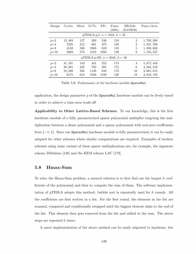
Design Cycles Slices LUTs FFs Fmax BRAMs Time×Area(MHz) (RAMB36)
qTESLA-p-I, n = 1024, h = 25
p=2 13, 404 127 393 240 134 2 1, 702, 308p=4 7225 212 661 375 138 3 1, 531, 700p=8 4133 336 1063 610 135 5 1, 388, 688p=16 2069 573 1819 1050 139 9 1, 185, 537
qTESLA-p-III, n = 2048, h = 40
p=2 41, 101 143 431 252 174 4 5, 877, 444p=4 20, 561 222 702 391 175 6 4, 564, 542p=8 10, 286 356 1138 643 173 10 3, 661, 815p=16 6175 618 1926 1109 138 18 3, 816, 150
Table 5.6: Performance of the hardware module SparseMul.
application, the design parameter p of the SparseMul hardware module can be freely tuned
in order to achieve a time-area trade-off.
Applicability to Other Lattice-Based Schemes. To our knowledge, this is the first
hardware module of a fully parameterized sparse polynomial multiplier targeting the mul-
tiplication between a dense polynomial and a sparse polynomial with non-zero coefficients
from {−1, 1}. Since our SparseMul hardware module is fully parameterized, it can be easily
adapted for other schemes where similar computations are required. Examples of modern
schemes using some variant of these sparse multiplications are, for example, the signature
scheme Dilithium [128] and the KEM scheme LAC [173].
5.8 Hmax-Sum
To solve the Hmax-Sum problem, a natural solution is to first find out the largest h coef-
ficients of the polynomial and then to compute the sum of them. The software implemen-
tation of qTESLA adopts this method: bubble sort is repeatedly used for h rounds. All
the coefficients are first written in a list. For the first round, the elements in the list are
scanned, compared and conditionally swapped until the biggest element sinks to the end of
the list. This element then gets removed from the list and added to the sum. The above
steps are repeated h times.
A naive implementation of the above method can be easily migrated to hardware, but
149
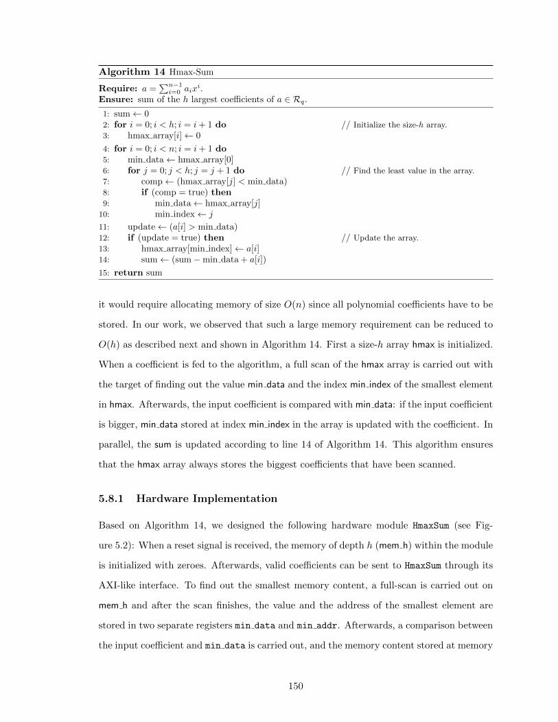
Algorithm 14 Hmax-Sum
Require: a =∑n−1i=0 aix
i.Ensure: sum of the h largest coefficients of a ∈ Rq.1: sum← 02: for i = 0; i < h; i = i+ 1 do // Initialize the size-h array.
3: hmax array[i]← 0
4: for i = 0; i < n; i = i+ 1 do5: min data← hmax array[0]6: for j = 0; j < h; j = j + 1 do // Find the least value in the array.
7: comp← (hmax array[j] < min data)8: if (comp = true) then9: min data← hmax array[j]
10: min index← j
11: update← (a[i] > min data)12: if (update = true) then // Update the array.
13: hmax array[min index]← a[i]14: sum← (sum−min data + a[i])
15: return sum
it would require allocating memory of size O(n) since all polynomial coefficients have to be
stored. In our work, we observed that such a large memory requirement can be reduced to
O(h) as described next and shown in Algorithm 14. First a size-h array hmax is initialized.
When a coefficient is fed to the algorithm, a full scan of the hmax array is carried out with
the target of finding out the value min data and the index min index of the smallest element
in hmax. Afterwards, the input coefficient is compared with min data: if the input coefficient
is bigger, min data stored at index min index in the array is updated with the coefficient. In
parallel, the sum is updated according to line 14 of Algorithm 14. This algorithm ensures
that the hmax array always stores the biggest coefficients that have been scanned.
5.8.1 Hardware Implementation
Based on Algorithm 14, we designed the following hardware module HmaxSum (see Fig-
ure 5.2): When a reset signal is received, the memory of depth h (mem h) within the module
is initialized with zeroes. Afterwards, valid coefficients can be sent to HmaxSum through its
AXI-like interface. To find out the smallest memory content, a full-scan is carried out on
mem h and after the scan finishes, the value and the address of the smallest element are
stored in two separate registers min data and min addr. Afterwards, a comparison between
the input coefficient and min data is carried out, and the memory content stored at memory
150

Module Cycles Slices LUTs FFs Memory Fmax(PRNG Incld.) (RAMB36) (MHz)
qTESLA-p-I
GaussSampler 18, 451 118 279 296 2.5 134HmaxSum 28, 686 27 83 66 0 356GaussSampler + HmaxSum 29, 293 144 362 360 2.5 130
qTESLA-p-III
GaussSampler 81, 335 191 470 490 4.5 123HmaxSum 88, 093 40 94 70 0 389GaussSampler + HmaxSum 88, 676 236 560 558 4.5 125
Table 5.7: Performance of the GaussSampler, HmaxSum, and GaussSampler + HmaxSum hardwaremodules; the last combination of modules gives the best performance due to parallelized execution.
address min addr is conditionally updated: If the input coefficient is larger, the memory
content stored at address min addr is overwritten with the coefficient value. In parallel, the
sum register is conditionally updated. After all the input coefficients of a polynomial are
processed by HmaxSum, the value of sum is returned as the result.
5.8.2 Evaluation
Apart from low memory requirements, another advantage of adopting Algorithm 14 is that
the HmaxSum module can run in parallel with the GaussSampler module. Once a valid
sample is generated by GaussSampler, HmaxSum can immediately start processing it. As
shown in Table 5.7, when running the HmaxSum module alone, it is quite expensive in terms
of cycles as the complexity of Algorithm 14 is O(n ·h). However, parallelizing the execution
of GaussSampler and HmaxSum leads to almost the same cycle count as running HmaxSum
alone. In terms of area utilization, the HmaxSum module is quite lightweight and, hence,
introduces a very small overhead.
5.9 Software-Hardware Co-Design of qTESLA
Based on the flexible hardware accelerators, we implemented a software-hardware co-design
of the qTESLA algorithm with provably secure parameter sets.
151

APB Decoder
Apb3GaussSamplerHmaxSum
Apb3GaussSampler
Apb3SHAKE
Apb3PolyMul
Apb3SparseMul
SHAKE
Wrapper
SHAKE
GaussSampler
Wrapper
SHAKE
GaussSampler
HmaxSum
Wrapper
ModMul
PolyMul
SparseMul
0x3000 0x3000 0x3000 0x4000 0x5000
Select one of the three modules dependingthe amount of acceleration desired
Figure 5.6: Detailed diagram of the connections between the APB Decoder, APB bridge modulesand hardware accelerators. Dotted squares all contain a SHAKE module and thus one peripheral fromthese three can be chosen depending on user’s requirements when a SHAKE accelerator is needed inthe design.
5.9.1 Prototype Platform
To demonstrate the effectiveness of the hardware accelerators, while targeting SoC type
designs with standard 32-bit interfaces, we prototyped the software-hardware co-design on
a RISC-V based Murax SoC, which was also used for prototyping the hash-based signature
scheme XMSS, as shown in Section 4.6.1.
5.9.2 Interface Between Software and Hardware
To accelerate the compute-intensive operations in qTESLA, the dedicated hardware accel-
erators described in the previous sections are added to the SoC as peripherals. The SoC
uses an 32-bit APB bus for connecting its peripherals to the main processor core. Our
hardware modules are connected to this APB bus, as shown in Figure 5.6.
5.10 Design Testing
For testing and verifying the functional correctness of the dedicated hardware accelerators
developed for lattice-based schemes, we adopt similar approaches as shown in Section 3.9.1.
152

USB-JTAG connection
to PC
USB-serial connection
to PC
Power SupplyTo FPGA
FMC Card
Artix 7 AC701 FPGA
Figure 5.7: Evaluation setup with an Artix-7 AC701 FPGA and an FMC XM105 Debug Card.
5.10.1 FPGA Evaluation Platform
We evaluated our design using an Artix-7 AC701 FPGA as test-platform which is a platform
recommended by NIST for PQC hardware evaluations. This board has a Xilinx XC7A200T-
2FBG676C device. We used Vivado Software Version 2018.3 for synthesis. Figure 5.7 shows
the evaluation setup for our experiments. Since the AC701 board has very limited number
of GPIOs pins, we connected an FMC XM105 Debug Card to the FMC connector on
the FPGA. This allows for sufficient GPIO pins to connect JTAG and UART to the SoC
instantiated in the FPGA (in addition to the usual JTAG used to program the FPGA itself).
We tested our implementations on the AC701 board at its default clock of 90 MHz. However,
to achieve a fair comparison, our speedup reports presented in the following sections are
based on the maximum frequency reported by the synthesis tools.
5.10.2 Hardware Prototype Setup
Further, to valid the design on FPGAs, we build a real-world prototype involving an FPGA
running the Murax SoC and the hardware accelerators, as well as a host computer. As
illustrated by Figure 5.7, the Murax SoC and the hardware accelerators run on the Artix-
7 FPGA which is connected to a host computer through the USB-JTAG and USB-serial
connections. Apart from the different FPGA models, this prototype setup is very similar
to the one that is used for evaluating the software-hardware co-design of XMSS (details are
available in Section 4.11.2).
153
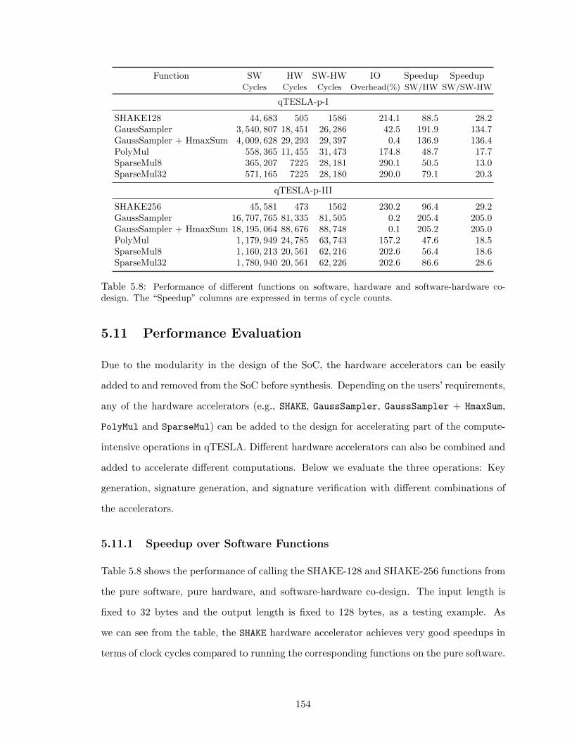
Function SW HW SW-HW IO Speedup SpeedupCycles Cycles Cycles Overhead(%) SW/HW SW/SW-HW
qTESLA-p-I
SHAKE128 44, 683 505 1586 214.1 88.5 28.2GaussSampler 3, 540, 807 18, 451 26, 286 42.5 191.9 134.7GaussSampler + HmaxSum 4, 009, 628 29, 293 29, 397 0.4 136.9 136.4PolyMul 558, 365 11, 455 31, 473 174.8 48.7 17.7SparseMul8 365, 207 7225 28, 181 290.1 50.5 13.0SparseMul32 571, 165 7225 28, 180 290.0 79.1 20.3
qTESLA-p-III
SHAKE256 45, 581 473 1562 230.2 96.4 29.2GaussSampler 16, 707, 765 81, 335 81, 505 0.2 205.4 205.0GaussSampler + HmaxSum 18, 195, 064 88, 676 88, 748 0.1 205.2 205.0PolyMul 1, 179, 949 24, 785 63, 743 157.2 47.6 18.5SparseMul8 1, 160, 213 20, 561 62, 216 202.6 56.4 18.6SparseMul32 1, 780, 940 20, 561 62, 226 202.6 86.6 28.6
Table 5.8: Performance of different functions on software, hardware and software-hardware co-design. The “Speedup” columns are expressed in terms of cycle counts.
5.11 Performance Evaluation
Due to the modularity in the design of the SoC, the hardware accelerators can be easily
added to and removed from the SoC before synthesis. Depending on the users’ requirements,
any of the hardware accelerators (e.g., SHAKE, GaussSampler, GaussSampler + HmaxSum,
PolyMul and SparseMul) can be added to the design for accelerating part of the compute-
intensive operations in qTESLA. Different hardware accelerators can also be combined and
added to accelerate different computations. Below we evaluate the three operations: Key
generation, signature generation, and signature verification with different combinations of
the accelerators.
5.11.1 Speedup over Software Functions
Table 5.8 shows the performance of calling the SHAKE-128 and SHAKE-256 functions from
the pure software, pure hardware, and software-hardware co-design. The input length is
fixed to 32 bytes and the output length is fixed to 128 bytes, as a testing example. As
we can see from the table, the SHAKE hardware accelerator achieves very good speedups in
terms of clock cycles compared to running the corresponding functions on the pure software.
154
Smaller speedups are achieved when the SHAKE module is added to the Murax SoC as an
accelerator due to the IO overhead for sending the inputs and returning the outputs between
the software and the hardware. With the IO overhead taken into account, function calls
to the SHAKE function in the “Murax + SHAKE” design still leads to an over 28× speedup
over the pure software implementation.
Table 5.8 also shows the performance of calling the Gaussian Sampler function from the
pure software, pure hardware, and software-hardware co-design. The input seed is fixed to
32 bytes and the output length is fixed to 1024 and 2048 for qTESLA-p-I and qTESLA-p-III,
respectively, as is the case in the qTESLA software reference implementation. As we can
see, when the Gaussian Sampler function is called in the design “Murax + GaussSampler”,
over 134× and 205× speedups are achieved compared to calling the functions on the pure
software for qTESLA-p-I and qTESLA-p-III, respectively. The reason for achieving such
high speedups is threefold: From the algorithm level, we adopted a binary-search based CDT
sampling algorithm in our design while the qTESLA software reference implementation uses
a more conservative full-scan based CDT sampling algorithm. In terms of implementation,
our fully pipelined hardware design brings a very good hardware acceleration over a pure
software-based implementation. Moreover, when the GaussSampler module is added as
an accelerator to the Murax SoC, the valid outputs from the hardware accelerator are
returned to the software in parallel with the hardware computation phase. In this case, the
IO overhead is very well hidden and the speedups brought by the hardware accelerator can
be well exploited.
Table 5.8 then shows the performance of calling the Gaussian Sampler and Hmax-Sum
functions from the pure software, pure hardware, and software-hardware co-design. As
we can see, when these two functions are called in the design “Murax + GaussSampler +
HmaxSum”, over 136× and 205× speedups are achieved compared to calling the functions
on the pure Murax SoC for qTESLA-p-I and qTESLA-p-III, respectively. We find it in-
teresting to note that by introducing a lightweight HmaxSum accelerator to the “Murax +
GaussSampler” design, the IO overhead for calling the Gaussian sampling function is almost
negligible as the output returning phase is perfectly overlapped with the computations of
the HmaxSum module.
155

Next, Table 5.8 shows the performance of calling the polynomial multiplication function
from the pure software, pure hardware, and software-hardware co-design. As shown in the
table, running one polynomial multiplication operation by use of the PolyMul accelerator
takes more than 47× less cycles compared to the pure software implementation. However,
when the function is called from the “Murax + PolyMul” design, two polynomials with large
coefficients have to be sent to the hardware and one polynomial has to be returned to the
software, leading to a rather big IO overhead. Therefore, only 17× and 18× speedups are
achieved for qTESLA-p-I and qTESLA-p-III, respectively.
Table 5.8 finally shows the performance of calling the sparse polynomial multiplication
functions SparseMul8 and SparseMul32 from the pure software, pure hardware, and software-
hardware co-design. As we can see, running one SparseMul8 operation by use of the hardware
accelerator takes the same number of cycles as running one SparseMul32 operation since the
same SparseMul module is used. When calling the sparse polynomial functions in the
“Murax + SparseMul” design, one polynomial with large coefficients and two small arrays
have to be sent to the hardware and one big polynomial has to be returned to the software,
yielding a big IO overhead. With these IO overhead taken into account, when the SparseMul8
and SparseMul32 functions are called in the “Murax + SparseMul” design, over 20× and
28× speedups are achieved compared to running the same function in pure software for
qTESLA-p-I and qTESLA-p-III, respectively.
5.11.2 Key Generation Evaluation
Table 5.9 shows the performance and maximum frequency of running qTESLA’s key gen-
eration on different designs. The cycles are reported as the average cycle counts for 100
executions. The column “speedup” reports the speedup of the time when adding the hard-
ware module(s) of the corresponding row compared to running on the pure Murax SoC
(first row). As we can see, adding a SHAKE accelerator gives over 2.4× and 2.2× speedups
compared to running the key generation operation on the pure Murax SoC for qTESLA-p-I
and qTESLA-p-III, respectively. Larger speedups are achieved when the GaussSampler
accelerator is added to the design as Gaussian sampling is the most compute-intensive op-
eration in the key generation step. By adding an extra lightweight HmaxSum accelerator into
156

Design Cycles Fmax Time Time×Area Speedup(MHz) (ms) (slice×ms)
qTESLA-p-I Key Generation
Murax 48, 529, 602 156 310.9 328, 299 1.00+ SHAKE 18, 214, 784 145 125.5 164, 472 2.48+ GaussSampler (incl. SHAKE) 6, 653, 608 137 48.7 73, 436 6.38+ GaussSampler + HmaxSum 2, 525, 853 126 20.1 30, 792 15.47+ PolyMul (incl. ModMul) 46, 933, 182 126 373.8 602, 596 0.83+ SparseMul 48, 529, 602 134 361.8 424, 795 0.86+ All 925, 431 121 7.7 18, 651 40.64
qTESLA-p-III Key Generation
Murax 297, 103, 198 156 1903.3 2, 009, 841 1.00+ SHAKE 120, 731, 265 145 831.5 1, 090, 134 2.29+ GaussSampler (incl. SHAKE) 28, 394, 350 126 224.8 350, 687 8.47+GaussSampler + HmaxSum 6, 494, 464 126 51.7 83, 606 36.79+ PolyMul (incl. ModMul) 292, 924, 220 125 2340.8 3, 829, 482 0.81+ SparseMul 297, 103, 153 161 1849.8 2, 199, 459 1.03+ All 2, 305, 220 121 19.0 47, 001 100.14
Table 5.9: Performance of qTESLA key generation on software and different software-hardwareco-designs. All = GaussSampler + HmaxSum + PolyMul + SparseMul. The “Speedup” column isprovided in terms of time.
Design Cycles Fmax Time Time×Area Speedup(MHz) (ms) (slice×ms)
qTESLA-p-I Signature Generation
Murax 47, 180, 534 156 302.2 319, 171 1.00+ SHAKE 22, 914, 215 145 157.8 206, 905 1.91+ GaussSampler (incl. SHAKE) 23, 348, 731 137 171.0 257, 697 1.77+ GaussSampler + HmaxSum 24, 580, 234 126 195.6 299, 647 1.55+ PolyMul (incl. ModMul) 34, 013, 026 126 270.9 436, 707 1.12+ SparseMul 41, 356, 497 134 308.4 362, 007 0.98+ All 4, 165, 160 121 34.4 83, 944 8.78
qTESLA-p-III Signature Generation
Murax 105, 525, 187 156 676.0 713, 865 1.00+ SHAKE 54, 013, 152 145 372.0 487, 710 1.82+ GaussSampler (incl. SHAKE) 55, 308, 030 126 437.9 683, 084 1.54+ GaussSampler + HmaxSum 53, 024, 762 126 422.4 682, 611 1.60+ PolyMul (incl. ModMul) 78, 377, 348 125 626.3 1, 024, 655 1.08+ SparseMul 86, 540, 888 161 538.8 640, 664 1.25+ All 7, 745, 088 121 63.9 157, 916 10.59
Table 5.10: Performance of qTESLA signature generation on software and different software-hardware co-designs. All = GaussSampler + HmaxSum + PolyMul + SparseMul. The “Speedup”column is provided in terms of time.
157

Design Cycles Fmax Time Time×Area Speedup(MHz) (ms) (slice×ms)
qTESLA-p-I Signature Verification
Murax 17, 871, 157 156 114.5 120, 895 1.00+ SHAKE 4, 625, 094 145 31.9 41, 763 3.59+ GaussSampler (incl. SHAKE) 4, 625, 505 137 33.9 51, 052 3.38+ GaussSampler + HmaxSum 4, 623, 861 126 36.8 56, 368 3.11+ PolyMul (incl. ModMul) 16, 274, 763 126 129.6 208, 960 0.88+ SparseMul 15, 793, 283 134 117.8 138, 243 0.97+ All 946, 520 121 7.8 19, 076 14.63
qTESLA-p-III Signature Verification
Murax 48, 309, 625 156 309.5 326, 810 1.00+ SHAKE 14, 899, 621 145 102.6 134, 535 3.02+ GaussSampler (incl. SHAKE) 14, 892, 149 126 117.9 183, 927 2.63+ GaussSampler + HmaxSum 14, 889, 776 126 118.6 191, 684 2.61+ PolyMul (incl. ModMul) 44, 130, 687 125 352.6 576, 934 0.88+ SparseMul 39, 915, 065 161 248.5 295, 490 1.25+ All 2, 315, 950 121 19.1 47, 220 16.21
Table 5.11: Performance of qTESLA signature verification on software and different software-hardware co-designs. All = GaussSampler + HmaxSum + PolyMul + SparseMul. The “Speedup”column is provided in terms of time.
the “Murax + GaussSampler” design, around 16× and 37× speedups are achieved which
is a larger improvement compared to adding a standalone GaussSampler accelerator in the
design. This is due to the fact that when the GaussSampler accelerator is added, the most
expensive Gaussian Sampler function gets greatly sped up and this in turn leaves the less
expensive Hmax-Sum function costly in the “Murax + GaussSampler” design. Interestingly,
while adding the PolyMul accelerator improves the cycle counts, the speedup compared to
running on the pure Murax SoC is 0.83, i.e., adding (only) PolyMul slows down the runtime.
This is due to the fact that the maximum frequency of the design drops when a hardware
accelerator is integrated. Adding a SparseMul accelerator to the Murax SoC does not bring
any speedup in terms of cycles as there is no sparse polynomial multiplication during key
generation. The best speedups are achieved when all the available hardware accelerators
are added (“Murax + All”): an around 40× speedup is achieved for qTESLA-p-I and an
around 100× speedup is achieved for qTESLA-p-III. The best time-area product for key
generation is also achieved in the “Murax + All” design.
158
5.11.3 Signature Generation and Verification Evaluation
Table 5.10 and Table 5.11 show the performance and maximum frequency of running the
qTESLA sign and verify operations on different designs. We report the average cycle counts
for 100 executions. The column “speedup” reports the speedup of the time when adding
the hardware module(s) of the corresponding row compared to running on the pure Murax
SoC (first row). As the signing and verification steps in qTESLA do not involve Gaussian
sampling, adding a GaussSampler accelerator to the design is equivalent to adding a SHAKE
accelerator. The small difference in the cycle counts comes from the wrapper function
that embeds SHAKE in the GaussSampler accelerator. Thus, the clock cycles achieved on a
“Murax + GaussSampler” design for signing and verification are similar to those achieved
on a “Murax + SHAKE” design. Apart from SHAKE computations, NTT-based polynomial
multiplication and sparse polynomial multiplication are two of the most compute-intensive
computations in signature generation and verification. As we can see from the tables,
adding a PolyMul accelerator to the design brings a good reduction in clock cycles (and a
speedup of 1.12) for signature generation compared to the pure software, while adding a
SparseMul accelerator improves the cycle counts for verification (leading to a speedup of
1.25). The best speedups are achieved when all available hardware accelerators are added
to the design (“Murax + All”): for qTESLA-p-III, speedups of 10.59× and 16.21× are
achieved for signing and verification operations, respectively. The best time-area product
for the signature generation and verification is also achieved in the “Murax + All” design.
5.12 Comparison with Related Work
In this section, we provide a detailed comparison with related work, including both software
and hardware implementations for digital signature schemes within the NIST standardiza-
tion process as well as digital signature schemes beyond NIST’s candidates.
5.12.1 Comparison to Other NIST’s Candidates
Table 5.12 provides a detailed comparison of our design with other designs targeting mod-
ern lattice-based digital signature schemes running on embedded systems. A thorough
159
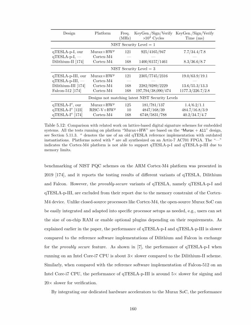
Design Platform Freq. KeyGen./Sign/Verify KeyGen./Sign/Verify(MHz) ×103 Cycles Time (ms)
NIST Security Level = 1
qTESLA-p-I, our Murax+HWp 121 925/4165/947 7.7/34.4/7.8qTESLA-p-I, — Cortex-M4 — — —Dilithium-II [174] Cortex-M4 168 1400/6157/1461 8.3/36.6/8.7
NIST Security Level = 3
qTESLA-p-III, our Murax+HWp 121 2305/7745/2316 19.0/63.9/19.1qTESLA-p-III, — Cortex-M4 — — —Dilithium-III [174] Cortex-M4 168 2282/9289/2229 13.6/55.3/13.3Falcon-512 [174] Cortex-M4 168 197,794/38,090/474 1177.3/226.7/2.8
Designs not matching latest NIST Security Levels
qTESLA-Io, our Murax+HWp 125 181/781/137 1.4/6.2/1.1qTESLA-Io [123] RISC-V+HWp 10 4847/168/39 484.7/16.8/3.9qTESLA-Io [174] Cortex-M4 168 6748/5831/788 40.2/34.7/4.7
Table 5.12: Comparison with related work on lattice-based digital signature schemes for embeddedsystems. All the tests running on platform “Murax+HW” are based on the “Murax + All” design,see Section 5.11.3. o denotes the use of an old qTESLA reference implementation with outdatedinstantiations. Platforms noted with p are all synthesized on an Artix-7 AC701 FPGA. The “—”indicates the Cortex-M4 platform is not able to support qTESLA-p-I and qTESLA-p-III due tomemory limits.
benchmarking of NIST PQC schemes on the ARM Cortex-M4 platform was presented in
2019 [174], and it reports the testing results of different variants of qTESLA, Dilithium
and Falcon. However, the provably-secure variants of qTESLA, namely qTESLA-p-I and
qTESLA-p-III, are excluded from their report due to the memory constraint of the Cortex-
M4 device. Unlike closed-source processors like Cortex-M4, the open-source Murax SoC can
be easily integrated and adapted into specific processor setups as needed, e.g., users can set
the size of on-chip RAM or enable optional plugins depending on their requirements. As
explained earlier in the paper, the performance of qTESLA-p-I and qTESLA-p-III is slower
compared to the reference software implementations of Dilithium and Falcon in exchange
for the provably secure feature. As shown in [7], the performance of qTESLA-p-I when
running on an Intel Core-i7 CPU is about 3× slower compared to the Dilithium-II scheme.
Similarly, when compared with the reference software implementation of Falcon-512 on an
Intel Core-i7 CPU, the performance of qTESLA-p-III is around 5× slower for signing and
20× slower for verification.
By integrating our dedicated hardware accelerators to the Murax SoC, the performance
160

of qTESLA-p-I on the “Murax +All” platform achieves a big improvement compared to
the pure software implementation, as shown in Table 5.12. As there is no existing work
on hardware designs of Dilithium, an apples-to-apples comparison between qTESLA on
hardware and Dilithium on hardware is currently not possible. However, if we regard the
performance of Dilithium-II running on the ARM Cortex-M4 device as being efficient, then
we can conclude that, with proper use of hardware accelerators, provably-secure schemes
like qTESLA can also be considered practical and that these schemes can be competitive
in terms of efficiency when running on embedded systems. In particular, running qTESLA-
p-III on “Murax +All” achieves a comparable efficiency to the Cortex-M4 benchmarking
result for Dilithium-III. When compared to the Falcon-512 scheme, qTESLA-p-III running
on our “Murax +All” platform is around 62× and 3.5× faster in terms of key generation
and signing time, respectively. Again, a fair comparison between qTESLA on hardware
and Falcon on hardware is currently not possible, as there is no publicly-available hardware
implementation of Falcon. However, we emphasize again that the proposed hardware ac-
celerators are not restricted to use in qTESLA and, hence, can benefit other schemes such
as Dilithium and Falcon. In summary, by taking advantage of the hardware acceleration,
the practical feasibility of running the provably-secure qTESLA variants qTESLA-p-I and
qTESLA-p-III on resource-constrained embedded systems is successfully demonstrated in
the present paper.
In 2019, a RISC-V based software-hardware co-design [123] focused on lattice-based
schemes was proposed and demonstrated the performance of some qTESLA variants with
prior heuristic parameters. As we can see in Table 5.12, as the design in [123] focuses on
low-power and low-cycles ASIC applications, their work presents very small clock cycles for
qTESLA-I signing and verification operations by packing more computations into one clock
cycle. However, such a design choice leads to a very low frequency; e.g., their software-
hardware co-design [123] can only run at 10MHz on an Artix-7 FPGA. Moreover, [123]
only partly accelerated qTESLA’s key generation since they followed the merge-sort based
CDT algorithm for Gaussian sampling as used in the reference software implementation.
To better compare our results with this design, we synthesized the “Murax +All” design for
161

qTESLA-I 2, modified the software reference implementation of qTESLA-I, and successfully
demonstrated its performance by running it on an Artix-7 FPGA. Given the much higher
frequency achieved in our design, as shown in Table 5.12, running qTESLA-I on our design
is 346×, 2.7×, and 3.5× faster for key generation, signature generation, and verification,
respectively, when compared to the results achieved in [123].
Hardware evaluations for other qTESLA instantiations using a High-Level Synthesis
(HLS)-based hardware design methodology have been also explored [175]. However, the
hardware designs generated by the HLS tool are too inefficient for embedded systems, e.g.,
for the smallest qTESLA-I parameters, it takes over 16× more LUTs compared to our
“Murax +All” design when synthesized on the same Artix-7 FPGA.
5.12.2 Comparison to Other Schemes
When comparing with hardware acceleration for schemes not submitted to NIST’s PQC
standardization effort, arguably the most important work is the RISC-V based software-
hardware co-design of XMSS [8] — a stateful hash-based scheme that was published as
Request for Comments (RFC) 8931 in 2018. Several hardware accelerators based on the
SHA256 hash function were provided in their work for accelerating the computations in
XMSS. Comparing performance of [8] with our qTESLA design paints about the same pic-
ture as for the original software implementations: While qTESLA’s key generation is much
faster, qTESLA’s sign and verification algorithms are slower compared to the corresponding
XMSS algorithms. Interestingly the speedup from SW to SW-HW is larger for qTESLA
than the speedup achieved for XMSS due to the efficient design of our GaussSampler ac-
celerator.
A few publications [131,176] also focused on the pure FPGA based implementation tar-
geting a specific lattice-based digital signature scheme. Their implementation only focuses
on the signing and verification operations. More importantly, their design only supports
fixed parameter set of (n, q) and this renders their hardware based designs not usable nowa-
days as the parameters and the construction of the schemes evolve.
2. We would like to emphasize that this result should only be used for comparison purposes since qTESLA-Iis outdated and withdrawn from the NIST submission.
162

5.13 Chapter Summary
This chapter presented a set of efficient and constant-time hardware accelerators for lattice-
based operations. All of the accelerators can be fully parameterized at compile-time for
different lattice-based schemes and security parameter sets. These flexible accelerators were
then used to implement the first software-hardware co-design of the provably-secure lattice-
based signature scheme qTESLA, namely qTESLA-p-I and qTESLA-p-III. The software-
hardware co-design demonstrated that with the hardware acceleration, the computationally
intensive qTESLA-p-I and qTESLA-p-III can run as fast or faster than other lattice-based
signature schemes (with smaller parameters or without provable parameters).
163

Chapter 6
Isogeny-based Cryptography:
Software-Hardware Co-Design of
SIKE
In this chapter, we focus on the post-quantum supersingular isogeny key encapsulation
(SIKE) scheme. SIKE, among various candidates in the NIST PQC standardization pro-
cess, is the only scheme from the isogeny-based family. Its uniqueness and the arithmetic
inherited from the popular ECC scheme have made SIKE a popular proposal. However, the
performance metrics of SIKE are not competitive when compared to other post-quantum
key encapsulation proposals. This chapter explores the potential of specialized hardware in
speeding up the compute-intensive operations in SIKE with the goal to make the hardware-
accelerated design more competitive with other schemes. Various elliptic curve and isogeny
hardware accelerators are designed to be versatile and parameterized in order to acceler-
ate the most compute-intensive operations in SIKE. We then present software-hardware
co-designs to demonstrate the efficiency of these hardware accelerators. In the end, we
successfully demonstrate the feasibility and efficiency of constructing hardware designs for
SIKE that is both FPGA-friendly and ASIC-friendly.
164

6.1 Background
In 2011, Jao and De Feo proposed a key exchange proposal called Supersingular Isogeny
Diffie-Hellman (SIDH) [53]. SIDH, in contrast to preceding public-key isogeny-based pro-
tocols [177–179], bases its security on the difficulty of computing an isogeny between two
isogenous supersingular elliptic curves defined over a field of characteristic p. However,
Galbraith et al. [180] showed that if one of the key exchange parties, e.g., Alice or Bob,
reuses a secret key for many protocol instances, a malicious attacker can then learn the
secret information through limited number of interactions. To defend against such attacks,
one of the solution is to force both parties in the SIDH protocol to use ephemeral secret
keys, e.g., each secret key is used only once, then gets discarded. Another solution is to
apply a generic passive-to-active transformation (e.g., the Fujisaki-Okamoto (FO) transfor-
mation [181]) to the protocol, and this will allow one of the two parties to use a long-term
secret key. This idea brings the Supersingular Isogeny Key Encapsulation (SIKE) proto-
col [182], which is the actively-secure version of Jao-De Feo’s SIDH key exchange proposal.
Among the third round candidates in the NIST PQC standardization process [183], the
SIKE protocol stands out by featuring the smallest public key sizes of all of the encryp-
tion and KEM candidates and by being the only isogeny-based submission. In its second
round status report, NIST highlighted that it sees SIKE “as a strong candidate for future
standardization with continued improvements” [184].
6.1.1 Related Work
Despite its relatively short security history, a few hardware designs have been proposed in re-
cent years targeting speeding up the popular SIKE scheme. In 2020, a performance-oriented
hardware design was proposed in [185]. This work presented a fast parallel architecture to
exploit the inherent parallelism of multiplication and addition operations within higher-level
elliptic curve and isogeny computations. As a pure hardware design, [185] achieved very
good performance in accelerating SIKE. However, on the contrary side, fixed architecture
also brings little flexibility in the design configuration. This issue can be problematic and
expensive for young and evolving cryptographic proposals such as SIKE. Another limitation
165

of this work is the heavy exploitation of the DSP architecture on specific FPGA models.
While this optimization improves the performance of the overall design on specific FPGAs,
it makes the hardware architecture less friendly when ported to ASIC.
A more compact design for SIKE [186] adopted the more flexible software-hardware
co-design approach. This design was presented in 2020 and used a customized 16-bit signed
and unsigned integer processor, and a wide multiplier accumulator (MAC) unit is added as
a closely-coupled coprocessor in the co-design. Compared to the high-performance design
in [185], this work is better suited for embedded applications and achieves a good time-area
trade-off. However, since the hardware accelerator (i.e., the MAC unit) was integrated into
the design in a closely-coupled fashion, porting these accelerators to another software or SoC
platform (e.g., RISC-V based SoCs or ARM based SoCs) becomes challenging. Furthermore,
similar to the design in [185], the design of the hardware accelerator in [186] relied heavily
on the configuration of the DSP blocks on a specific FPGA model. This feature makes
porting the design to ASIC platforms difficult.
6.1.2 Motivation for Our Work
In this work, we focus on the design and implementation of efficient and flexible hardware
accelerators for isogeny-based cryptography. Apart from good performance and compact
area, the design of these accelerators also takes a few other features into account. The
first feature enabled in our design is portability since standard interfaces are required to
make sure that the accelerators can be ported among standard platforms with minimal
modifications. This design feature is important for exploring the performance of hardware
designs for young cryptographic proposals on different platforms. Another feature taken
into account in the design is flexibility since the use of SIKE hardware will be required
in many different applications. Usually different applications require different trade-offs
between time and area when choosing the specific hardware design. Therefore, unlike much
of prior work, the accelerators developed in this work are designed to be fully parameterized
at compile-time to help implement different security parameters and support flexible design
configurations targeting different user applications. Furthermore, the final target of these
accelerators are ASIC platforms, therefore, we do not exploit the structures of DSP blocks
166

nor any other available hard blocks on FPGA platforms. These isogeny-based cryptography
accelerators are then used to build an efficient software-hardware co-design for speeding up
the computations of SIKE.
This chapter is partly based on our work [10]. The contributions and organizations of
this chapter are as follows:
• We give an introduction in Section 6.2 to the relevant aspects of the SIKE scheme.
• We present efficient hardware implementations for the prime field arithmetic and
extension field arithmetic in Section 6.3.
• We develop several hardware accelerators to speed up the most expensive elliptic curve
and isogeny operations in SIKE, details are presented in Section 6.4. These hardware
accelerators achieve a significant speedup compared to running the corresponding
functions on pure software.
• In Section 6.5, we show how to integrate SIKE hardware accelerators into the SoC
and present an efficient software-hardware co-design of SIKE based on the SoC.
• The evaluation results and the comparison results with related work in Section 6.6
and Section 6.7, respectively, successfully demonstrate the efficiency of our customized
hardware accelerators through the speedups achieved by the software-hardware co-
design of SIKE.
• In the end, a short summary for this chapter is given in Section 6.8.
6.2 SIDH and SIKE
SIDH and SIKE are based on a problem – called the computational supersingular isogeny
(CSSI) problem in [56] – that is more special than the general problem of constructing an
isogeny between two supersingular curves. In these protocols, the degree of the isogeny is
smooth and public, and both parties in the key exchange each publish two images of some
fixed points under their corresponding secret isogenies. However, so far no attack has been
able to advantageously exploit this extra information.
167

!
"#
"(a) Isogeny.
!"
!#$
%&
%&
%'
%'
%'
%'
%&
%&
!$#
PKAPKB!$
!#
(b) The SIDH protocol.
Figure 6.1: Diagram of a supersingular isogeny graph, an isogeny, and the SIDH protocol.
6.2.1 Notation
SIDH is defined in the quadratic extensions of large prime fields Fp. Typically, the most
convenient representation is adopted as Fp2 = Fp(i) with i2 + 1 = 0 and elements from the
extension field accordingly have form a0 + a1 · i where a0, a1 ∈ Fp.
Before introducing the SIDH and the SIKE protocols, a few terminologies are described
from the high-level as follows. For more formal and detailed descriptions on SIDH and
SIKE, please refer to the SIKE specification [9] and tutorial [187].
j-invariant. Every elliptic curve has a unique j-invariant, which can be regarded as the
unique property of a curve. For example, Montgomery form [188]
Ea : y2 = x3 + ax2 + x (6.1)
have j-invariant
j(Ea) =256(a2 − 3)3
(a2 − 4)(6.2)
Isomorphism Class. An isomorphism class contains a set of elliptic curves and these
curves all have the same j-invariant. In another word, two elliptic curves are isomorphic to
each other if and only if they have the same j-invariant.
Isogeny. An isogeny defines the mapping from one elliptic curve to another (as shown in
Figure 6.1a):
φ : E1 → E (6.3)
168
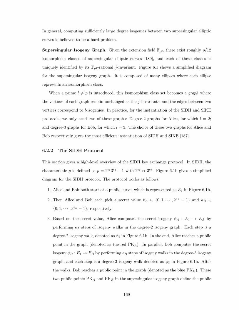
In general, computing sufficiently large degree isogenies between two supersingular elliptic
curves is believed to be a hard problem.
Supersingular Isogeny Graph. Given the extension field Fp2 , there exist roughly p/12
isomorphism classes of supersingular elliptic curves [189], and each of these classes is
uniquely identified by its Fp2-rational j-invariant. Figure 6.1 shows a simplified diagram
for the supersingular isogeny graph. It is composed of many ellipses where each ellipse
represents an isomorphism class.
When a prime l 6= p is introduced, this isomorphism class set becomes a graph where
the vertices of each graph remain unchanged as the j-invariants, and the edges between two
vertices correspond to l-isogenies. In practice, for the instantiation of the SIDH and SIKE
protocols, we only need two of these graphs: Degree-2 graphs for Alice, for which l = 2;
and degree-3 graphs for Bob, for which l = 3. The choice of these two graphs for Alice and
Bob respectively gives the most efficient instantiation of SIDH and SIKE [187].
6.2.2 The SIDH Protocol
This section gives a high-level overview of the SIDH key exchange protocol. In SIDH, the
characteristic p is defined as p = 2e23e3 − 1 with 2e2 ≈ 3e3 . Figure 6.1b gives a simplified
diagram for the SIDH protocol. The protocol works as follows:
1. Alice and Bob both start at a public curve, which is represented as E1 in Figure 6.1b.
2. Then Alice and Bob each pick a secret value kA ∈ {0, 1, · · · , 2eA − 1} and kB ∈
{0, 1, · · · , 3eB − 1}, respectively.
3. Based on the secret value, Alice computes the secret isogeny φA : E1 → EA by
performing eA steps of isogeny walks in the degree-2 isogeny graph. Each step is a
degree-2 isogeny walk, denoted as φ2 in Figure 6.1b. In the end, Alice reaches a public
point in the graph (denoted as the red PKA). In parallel, Bob computes the secret
isogeny φB : E1 → EB by performing eB steps of isogeny walks in the degree-3 isogeny
graph, and each step is a degree-3 isogeny walk denoted as φ3 in Figure 6.1b. After
the walks, Bob reaches a public point in the graph (denoted as the blue PKB). These
two public points PKA and PKB in the supersingular isogeny graph define the public
169

keys of Alice and Bob, respectively.
4. Once the public keys are computed, Alice and Bob exchange their public keys.
5. Afterwards, given Bob’s public key and her own secret value kA, Alice computes
another secret isogeny φ′A : EB → EAB. Similarly, Bob also computes a new secret
isogeny as φ′B : EA → EBA.
6. At this point, Alice and Bob each computes the shared key as jAB = j(EAB) and
jBA = j(EBA) where jAB = jBA. In another word, the j-invariant of the final landed
isomorphism class is computed as the shared secret between Alice and Bob. The SIDH
protocol ensures that after performing the rest of the isogeny walks, Alice and Bob
land in the same point, or the same isomorphism class in the graph.
Note that the protocol descriptions above are simplified and omit the details such as the
exchange of the images of Alice’s and Bob’s public basis points. A complete explanation of
the protocol is available from [187].
6.2.3 The SIKE Protocol
SIKE [9] applies a generic transformation to SIDH in order to allow one party to safely use
a long-term secret key. For example, in order to allow Alice to use a long-term secret key
kA, Bob first needs to compute his secret key kB as the output of a cryptographic hash
function given Alice’s public key PKA and a randomly chosen value m:
kB = H(PKA,m) (6.4)
Afterwards, Bob needs to use Alice’s fixed public key PKA and his own secret key kB to
compute the shared secret j following the regular procedures. Once this shared secret is
computed, Bob can start sending the following information
(PKB, H′(j)⊕m) (6.5)
to Alice where PKB is his public key, m is the previously chosen random value, and H ′(j)
computes the hash digest of the shared secret key.
170
On Alice’s side, once she receives this message, she can use Bob’s public key and her
secret key to compute j and then H(j), and this will help her recover Bob’s random value m.
Afterwards, she can use m and her own public key to recover Bob’s secret key kB following
Equation 6.4. Then she can recompute Bob’s public key and check if the computed result
matches the value of PKB contained in Bob’s message. If this check succeeds, Alice can
be assured that Bob is not acting maliciously, and she can perform the rest of the steps.
Otherwise, she can simply output garbage and send it to Bob. In this case, Bob still receives
messages, but he is not able to learn anything about Alice’s secrets.
6.3 Field Arithmetic
The computations in SIKE are based on finite field arithmetic on the extension field Fp2 .
In this section, we introduce the basic arithmetic on this field, further, we present efficient
hardware implementation for the Fp2 multiplication building block.
6.3.1 Fp2 Addition
As explained in Section 6.2.1, elements from the extension field have the form a = a0+a1 ·i ∈
Fp2 with a0, a1 ∈ Fp and i2 + 1 = 0. If we fix the basis {1, i} of Fp2 as a 2-dimensional
vector space over Fp, we can further represent the above element a as a vector (a0, a1). In
this case, the addition of two elements a = (a0, a1) and b = (b0, b1) in Fp2 can be simply
computed as follows:
a+ b = (a0, a1) + (b0, b1) = (a0 + a1, b0 + b1) (6.6)
Subtraction operations on Fp2 can be computed in a similar fashion:
a− b = (a0, a1)− (b0, b1) = (a0 − a1, b0 − b1) (6.7)
Therefore, an addition (or subtraction) operation on Fp2 can be simply realized by carrying
out two addition (or subtraction) operations on Fp.
171

Figure 6.2: Schoolbook and Karatsuba multiplication algorithms for Fp2 multiplication.
6.3.2 Fp2 Multiplication
A multiplication operation on Fp2 is given as follows:
a · b = (a0, a1) · (b0, b1) = (a0 · a1 − a1 · b1, a0 · b1 + a1 · b0) (6.8)
As shown in Equation 6.8, when following the schoolbook algorithm, each Fp2 multiplication
operation costs four Fp multiplications and two Fp additions (or subtractions). Another
typical approach is to adopt the Karatsuba algorithm [80]. The main goal of this algorithm
is to reduce the number of multiplications by trading with adding a few more addition
and subtraction operations. When using this method, the multiplication operation can be
realized with three Fp multiplications and five Fp additions (or subtractions) as follows:
a · b = (a0, a1) · (b0, b1) = ((a0 · b0)− (a1 · b1)), ((a0 +a1) · (b0 + b1)− (a0 · b0)− (a1 · b1)) (6.9)
Compared to the schoolbook approach, the Karatsuba method eliminates one Fp multi-
plication operation while adding few extra Fp addition and subtraction operations. Since
multiplications are the most expensive operation in Fp, the Karatsuba method is more com-
monly adopted for Fp2 multiplications. However, as depicted in Figure 6.2, the dataflow in
the Karatsuba method has more dependent operations which also leads to slightly longer
latency. This data dependency can become an issue when designing a pipelined architecture
for the Fp2 multiplication unit; further, data scheduling becomes much more complex in this
approach. Therefore, in our hardware design, we adopt the simpler schoolbook approach.
172

Algorithm 15 Modified FIOS algorithm for Montgomery Multiplier in Fp2[for computing: c0 = (a0 · b0 − a1 · b1) mod p]
Require: operands a0, a1, b0, b1, each of n digits, each digits ∈ [0, 2r) for radix of r bits.m = p+ 1, λ: number of 0 digits in m.
Ensure: [t0, · · · , tn−1]← MontRed(a0 · b0 − a1 · b1)
1: for i = 1, . . . , n− 1 do2: (C, S) = a0,0 · b0,i − a1,0 · b1,i + t03: mm = S4: for j = 1, . . . , n− 1 do5: if j < λ then // optimizations for 0 digits in m
6: (C, S) = a0,j · b0,i − a1,j · b1,i + tj + C7: else // mult. integrated with reduction
8: (C, S) = a0,j · b0,i − a1,j · b1,i +mm ·mj + tj + C
9: tj−1 = S
10: tn−1 = C
11: return [t0, · · · , tn−1]
Algorithm 16 Modified FIOS algorithm for Montgomery Multiplier in Fp2[for computing: c1 = (a0 · b1 + a1 · b0) mod p]
Require: operands a0, a1, b0, b1, each of n digits, each digits ∈ [0, 2r) for radix of r bits.m = p+ 1, λ: number of 0 digits in m.
Ensure: [t0, · · · , tn−1]← MontRed(a0 · b1 + a1 · b0)
1: for i = 1, . . . , n− 1 do2: (C, S) = a0,0 · b1,i + a1,0 · b0,i + t03: mm = S4: for j = 1, . . . , n− 1 do5: if j < λ then // optimizations for 0 digits in m
6: (C, S) = a0,j · b1,i + a1,j · b0,i + tj + C7: else // mult. integrated with reduction
8: (C, S) = a0,j · b1,i + a1,j · b0,i +mm ·mj + tj + C
9: tj−1 = S
10: tn−1 = C
11: return [t0, · · · , tn−1]
6.3.2.1 Optimized Schoolbook Approach for Fp2 Multiplication
As shown in Section 6.3.2, Fp2 multiplications can be further decomposed into multiplica-
tions, additions, and subtractions on the prime field Fp. To be more specific, Fp multipli-
cations are modular multiplications (a0 · b0) mod p where a0, b0 ∈ Fp. Montgomery multi-
plication [172] is commonly adopted for performing fast modular multiplications. Within
one Montgomery multiplication, one integer multiplication is first carried out, followed by
a Montgomery reduction operation which can be implemented by use of one integer multi-
plication and a few other much cheaper computations.
Since the characteristic p of the field used in SIKE is pretty large, e.g., the smallest
173

Controller
+–
+–
step_sub step_add
mem mem
mem mem mem mem mem
a0 a1 b0 b1 m
sub result
add result
input data
output data
Multiplier core
Figure 6.3: Diagram of the Fp2 Multiplier. Light grey boxes represent input data memory blocks,and dark grey boxes represent output result memory blocks.
parameter set SIKEp434 is defined with p of 434 bits [9]. In this case, a direct multiplication
on the wide input operands is hard to carry out.
For our design, for the extension field multiplication, we propose a modified Finely
Integrated Operand Scanning (FIOS) algorithm [190] which is a multi-precision schoolbook
based Montgomery multiplication algorithm. In this algorithm, input operands a0, a1, b0,
and b1 are divided into n = d log2pt e digits and each digit ∈ [0, 2r) is of radix of r bits. m is a
constant value determined by p, and λ is the number of zero digits in m. Algorithm 15 shows
the computation result for the left half of the Fp2 multiplication while Algorithm 16 shows
the right half of the result. An important optimization is applied based on our observation
that each half of the Fp2 multiplication computes two modular Fp multiplications before the
results are sent further for the final Fp addition (or subtraction). Inspired by this, we merge
the two reduction operations (required by the two Fp multiplications) into one. This simple
yet effective optimization helps eliminate one integer multiplication within each half of the
Fp2 multiplication (see line 8 of Algorithm 15 and line 8 of Algorithm 16). Compared to the
Karatsuba algorithm, our optimized schoolbook approach for Fp2 multiplication takes the
same number of integer multiplication operations; however, without introducing complex
data depencies in the data flow. This optimization is integrated to the inner loop of the
algorithm where multiplication and reduction operations are integrated. The inner loop is
then repeated for n2 times by scanning each digit of operand a and b, respectively.
174

6.3.2.2 Hardware Implementation
The hardware design of the Montgomery multiplier is based on the modified FIOS algorithm.
A simplified diagram demonstrating the architecture of the Fp2 Multiplier is presented in
Figure 6.3. The input operands a0, a1, b0, b1 and the constant value m are all stored in
memory blocks of width r and depth n where r is the size of the radix and n is the number
of digits. Two separate modules step sub and step add are implemented for realizing the
innerloop computations in Algorithm 15 and Algorithm 16 respectively. As shown in line 8
of Algorithm 15, the innerloop involves three integer multiplications and a few addition and
subtraction operations. In our design, in the step sub module, three integer multipliers are
instantiated to realize these multiplications in parallel. The design of the step add module is
very similar to the step sub module, despite that the input operands are different and that
the inner subtraction operations are replaced with additions. Apart from the step sub and
step add modules, a controller module is also needed to coordinate the memory accesses
as well as the interactions between the memory blocks and the computation units. Built up
on these computational units, input data memory blocks, as well as output result memory
blocks, we present an efficient module Fp2 Multiplier for the Montgomery multiplier.
The Fp2 Montgomery multiplier is very flexible: Depending on the SIKE security pa-
rameters and performance requirements of a specific application, users can choose the pa-
rameters, namely the number of digitis n and the radix r. Further, the hardware design of
the multiplier is very lightweight. Apart from the 6 integer multipliers arranged to enable
parallel computations of the subtraction and addition parts of the multiplication result, we
only need a small amount of control logic to handle the loops of the FIOS algorithm. In the
end, since our design is fully pipelined, in total it takes around n2 cycles for one complete
Fp2 multiplication.
6.3.2.3 Performance Evaluation
Table 6.1 shows the performance of the hardware module Fp2 Multiplier for the SIKEp434
parameter set. The synthesis results are collected from a Virtex-7 690T FPGA. When DSP
units are enabled during synthesis, we can easily see that the Montgomery multiplier is very
175

Radix Digits Cycles Slices/LUTs/FFs DSPs Fmax Time×Arear n (MHz)
SIKEp434, with DSPs
16 28 872 143/436/396 6 260 0.47932 14 242 361/1060/1078 24 193 0.45364 7 82 859/2593/2228 96 123 0.57524 19 442 227/612/690 12 249 0.40434 13 224 388/1222/1210 24 195 0.44551 9 120 573/1700/1680 54 138 0.500
SIKEp434, without DSPs
16 28 872 667/2200/684 0 222 2.6232 14 242 2076/7260/1301 0 171 2.9364 7 82 7464/27757/3186 0 118 5.1924 19 442 1295/4350/996 0 196 2.9234 13 224 2398/8392/1448 0 160 3.3551 9 120 4765/17057/2288 0 130 4.41
Table 6.1: Performance of the hardware module Fp2 Multiplier for SIKEp434 (synthesized withand without DSPs on a Virtex-7 690T FPGA).
lightweight in terms of area consumption while a good performance is achieved. As shown
in the table, radix r can be freely tuned to achieve a tradeoff between time and area. In
general, as radix r grows, the cycle counts get reduced; however, the improved performance
comes with a big cost in area and longer logical paths. Note that in our hardware design
of the Montgomery multiplier, the value of the radix r is not constrained to a power of 2.
In general, if the targeted platform is FPGA, users can choose radix in a way that is better
tailored to the structure of the DSP units on the specific FPGA model. For example, radix
r ∈ {24, 34, 51} can be chosen as FPGA-friendly configurations targeting an Virtex-7 690T
FPGA which has DSP blocks of size 18× 25 [191]. Based on the evaluation results, we can
see that these FPGA-friendly radix values lead to better time-area products.
As illustrated in Section 6.1.2, one of the main motivation behind this work is to provide
efficient hardware accelerators for SIKE that are both FPGA-friendly and ASIC-friendly.
Therefore we also present results for the Montgomery multiplier with DSP units disabled
during the synthesis to gain a good understanding about the best-achievable performance
on ASIC platforms. Compared to the results achieved with DSP units enabled, our eval-
uation results show that the area consumption of the Montgomery multiplier increases a
lot especially for big radix values as dedicated logic is needed for synthesizing expensive
176
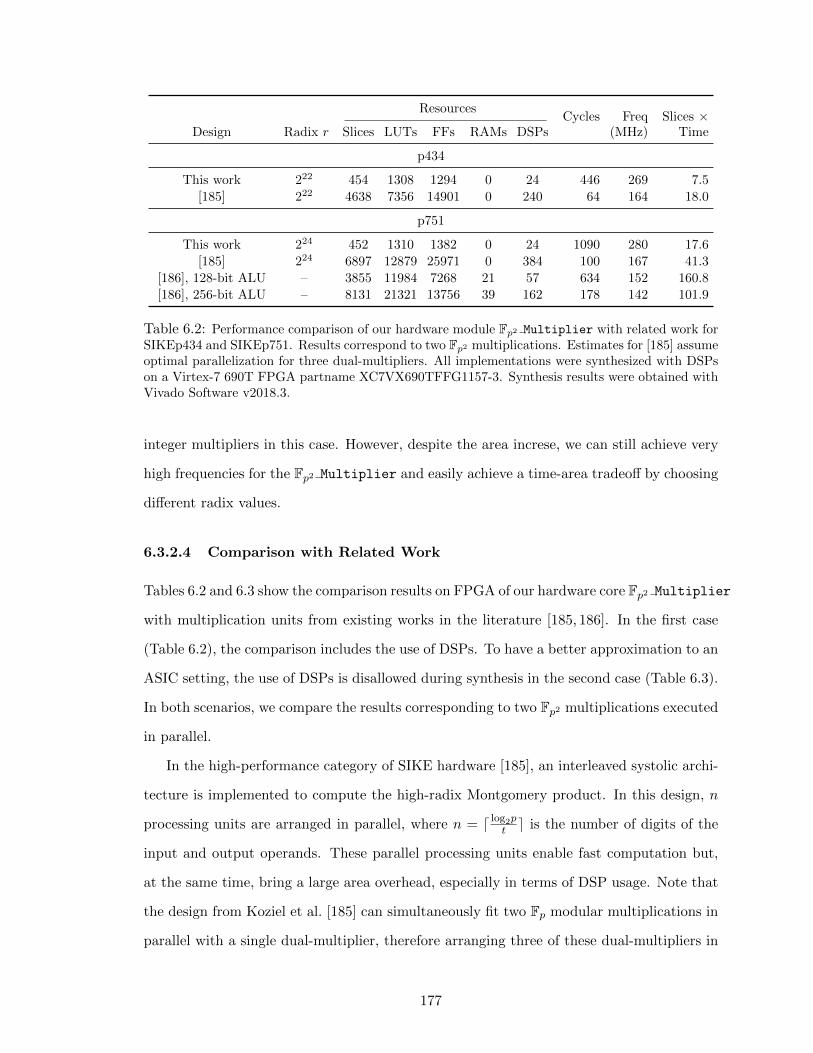
ResourcesCycles Freq Slices ×
Design Radix r Slices LUTs FFs RAMs DSPs (MHz) Time
p434
This work 222 454 1308 1294 0 24 446 269 7.5
[185] 222 4638 7356 14901 0 240 64 164 18.0
p751
This work 224 452 1310 1382 0 24 1090 280 17.6
[185] 224 6897 12879 25971 0 384 100 167 41.3
[186], 128-bit ALU – 3855 11984 7268 21 57 634 152 160.8
[186], 256-bit ALU – 8131 21321 13756 39 162 178 142 101.9
Table 6.2: Performance comparison of our hardware module Fp2 Multiplier with related work forSIKEp434 and SIKEp751. Results correspond to two Fp2 multiplications. Estimates for [185] assumeoptimal parallelization for three dual-multipliers. All implementations were synthesized with DSPson a Virtex-7 690T FPGA partname XC7VX690TFFG1157-3. Synthesis results were obtained withVivado Software v2018.3.
integer multipliers in this case. However, despite the area increse, we can still achieve very
high frequencies for the Fp2 Multiplier and easily achieve a time-area tradeoff by choosing
different radix values.
6.3.2.4 Comparison with Related Work
Tables 6.2 and 6.3 show the comparison results on FPGA of our hardware core Fp2 Multiplier
with multiplication units from existing works in the literature [185, 186]. In the first case
(Table 6.2), the comparison includes the use of DSPs. To have a better approximation to an
ASIC setting, the use of DSPs is disallowed during synthesis in the second case (Table 6.3).
In both scenarios, we compare the results corresponding to two Fp2 multiplications executed
in parallel.
In the high-performance category of SIKE hardware [185], an interleaved systolic archi-
tecture is implemented to compute the high-radix Montgomery product. In this design, n
processing units are arranged in parallel, where n = d log2pt e is the number of digits of the
input and output operands. These parallel processing units enable fast computation but,
at the same time, bring a large area overhead, especially in terms of DSP usage. Note that
the design from Koziel et al. [185] can simultaneously fit two Fp modular multiplications in
parallel with a single dual-multiplier, therefore arranging three of these dual-multipliers in
177

ResourcesCycles Freq Slices ×
Design Radix r Slices LUTs FFs RAMs (MHz) Time
p434
This work 222 2302 7882 1838 0 446 205 50.1
[185] 222 18669 55188 15033 0 64 122 98.0
p751
This work 224 2526 8776 1994 0 1090 195 141.2
[185] 224 34794 101898 26115 0 100 123 283.0
[186], 128-bit ALU – 7131 23417 8080 6 634 161 281.2
[186], 256-bit ALU – 24188 81503 18004 0 178 159 270.3
Table 6.3: Performance comparison of our hardware module Fp2 Multiplier with related workfor SIKEp434 and SIKEp751. Results correspond to two Fp2 multiplications. Estimates for [185]assume optimal parallelization for three dual-multipliers. All implementations were synthesizedwithout DSPs on a Virtex-7 690T FPGA partname XC7VX690TFFG1157-3. Synthesis results wereobtained with Vivado Software v2018.3.
parallel can enable the computation of two parallel Fp2 multiplications (assuming the use
of Karatsuba algorithm). As shown in Table 6.2, our implementation takes less than 8×
and 13× the number of slices and DSPs that Koziel et al. [185] require, respectively, which
translates to much smaller time-area products. This is achieved even considering that our
estimates for [185] assume optimal parallelization of multiplications in their implementation,
which is not always achieved due to their complex scheduling design.
The comparison results with the compact SIKE hardware design by Massolino et al. [186]
are also included in the tables. Since the multiplier accumulator (MAC) unit from [186]
is designed to be unified for all the Round 3 SIKE parameter sets, for a fair comparison
we only consider the largest SIKE parameter set, namely SIKEp751. Their MAC unit can
be configured as either 128-bit or 256-bit to provide different time-area trade-offs. Note
that in both cases the MAC unit features an 8-stage pipeline architecture, thus, it is able
to perform 8 Fp multiplications in parallel corresponding to two Fp2 multiplications. The
results show that our hardware multiplier is significantly more lightweight in terms of slices,
memory usage and DSP blocks, while it also achieves much better time-area products.
178
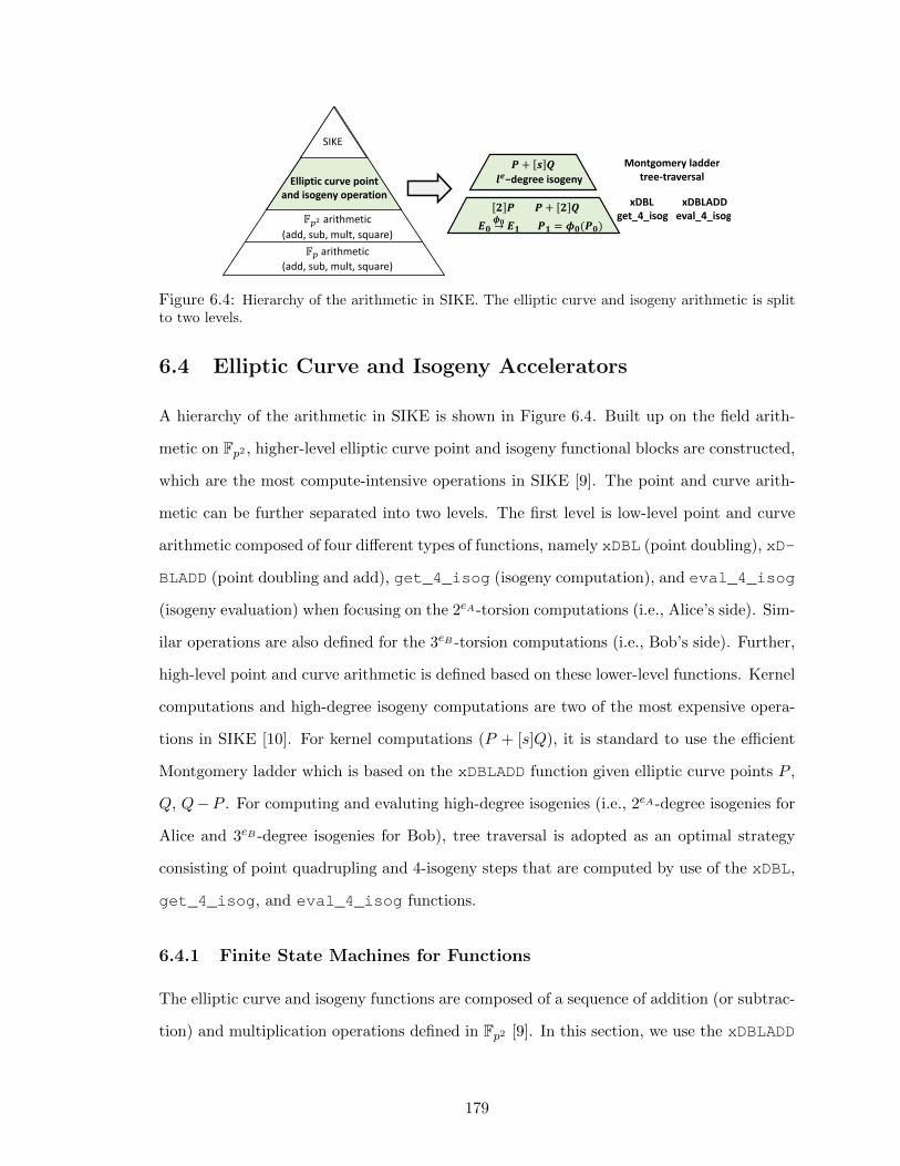
!" arithmetic(add, sub, mult, square)
!"# arithmetic(add, sub, mult, square)
Elliptic curve point and isogeny operation
SIKE
$ + & '()−degree isogeny
* $ $ + * '+, → +. $. = 0,($,)0,
Montgomery laddertree-traversal
xDBL xDBLADDget_4_isog eval_4_isog
Figure 6.4: Hierarchy of the arithmetic in SIKE. The elliptic curve and isogeny arithmetic is splitto two levels.
6.4 Elliptic Curve and Isogeny Accelerators
A hierarchy of the arithmetic in SIKE is shown in Figure 6.4. Built up on the field arith-
metic on Fp2 , higher-level elliptic curve point and isogeny functional blocks are constructed,
which are the most compute-intensive operations in SIKE [9]. The point and curve arith-
metic can be further separated into two levels. The first level is low-level point and curve
arithmetic composed of four different types of functions, namely xDBL (point doubling), xD-
BLADD (point doubling and add), get_4_isog (isogeny computation), and eval_4_isog
(isogeny evaluation) when focusing on the 2eA-torsion computations (i.e., Alice’s side). Sim-
ilar operations are also defined for the 3eB -torsion computations (i.e., Bob’s side). Further,
high-level point and curve arithmetic is defined based on these lower-level functions. Kernel
computations and high-degree isogeny computations are two of the most expensive opera-
tions in SIKE [10]. For kernel computations (P + [s]Q), it is standard to use the efficient
Montgomery ladder which is based on the xDBLADD function given elliptic curve points P ,
Q, Q−P . For computing and evaluting high-degree isogenies (i.e., 2eA-degree isogenies for
Alice and 3eB -degree isogenies for Bob), tree traversal is adopted as an optimal strategy
consisting of point quadrupling and 4-isogeny steps that are computed by use of the xDBL,
get_4_isog, and eval_4_isog functions.
6.4.1 Finite State Machines for Functions
The elliptic curve and isogeny functions are composed of a sequence of addition (or subtrac-
tion) and multiplication operations defined in Fp2 [9]. In this section, we use the xDBLADD
179

def xDBLADD(XP,ZP,XQ,ZQ,xPQ,A24):t0 = XP+ZPt1 = XP-ZPt2 = XQ+ZQt3 = XQ-ZQt6 = t0*t3 t7 = t1*t2 t2 = t0^2 t3 = t1^2 t0 = t2-t3t1 = t6-t7t4 = A24*t0 t5 = t2*t3 t2 = t4+t3t8 = t6+t7t3 = t1^2 t4 = t8^2 t1 = t2*t0 t6 = xPQ*t3 return t5,t1,t4,t6
(a) Software-friendlyversion.
def xDBLADD_FSM(XP,ZP,XQ,ZQ,xPQ,zPQ,A24):t0 = XP+ZPt1 = XP-ZP t4 = t0t5 = t1 t0 = XQ+ZQt1 = XQ-ZQt2 = t1*t4 t3 = t0*t5 t6 = t2t7 = t3t2 = t4^2 t3 = t5^2 t4 = t2 t5 = t3 t0 = t2-t3t1 = t6-t7t8 = t0 t9 = t1
t2 = t4*t5 t3 = t0*A24 t10 = t2 t4 = t3t0 = t5+t3 t1 = t6+t7 t2 = t1^2 t3 = t9^2 t4 = t2 t5 = t3t2 = t0*t8 t3 = xPQ*t5 t5 = t2 t2 = t4*zPQXP = t10ZP = t5XQ = t2ZQ = t3return XP,ZP,XQ,ZQ
(b) Hardware-friendly ver-sion.
def xDBLADD_FSM(XP,ZP,XQ,ZQ,xPQ,zPQ,A24):t0 = XP+ZPt1 = XP-ZP t4 = t0t5 = t1 t0 = XQ+ZQt1 = XQ-ZQt2 = t1*t4 t3 = t0*t5 t6 = t2t7 = t3t2 = t4^2 t3 = t5^2 t4 = t2 t5 = t3 t0 = t2-t3t1 = t6-t7t8 = t0 t9 = t1
t2 = t4*t5 t3 = t0*A24 t10 = t2 t4 = t3t0 = t5+t3 t1 = t6+t7 t2 = t1^2 t3 = t9^2 t4 = t2 t5 = t3t2 = t0*t8 t3 = xPQ*t5 t5 = t2 t2 = t4*zPQXP = t10ZP = t5XQ = t2ZQ = t3return XP,ZP,XQ,ZQ
(c) Pseudocode split intostates.
Figure 6.5: Reference pseudocode in Sage for xDBLADD.
function as an example to demonstrate how to construct efficient hardware architectures
for these functions.
Figure 6.5 shows the software reference code for the xDBLADD function. One of the
key observation we made based on the pseudocode is that two addition (or subtraction)
operations or two multiplication (or squaring) operations oftentimes happen in parallel.
Therefore, in our hardware design, we arrange two Fp2 adders and two Fp2 multipliers in
parallel. Based on the pseudocode, we can easily build a Finite State Machine (FSM) [192]
by splitting the computation steps into chunks where each chunk is handled by one state
in the FSM. Mapping the ideas above to hardware can be realized in a straightforward
way, as follows: Initially, input operands P, Q, PQ and A24 are all initialized and stored
in memory blocks. First, two adders are triggered to compute the t0 = XP + ZP and t1
= XP - ZP steps in parallel. Once the computations are finished, the result memories of
adders are updated with t0 and t1. In the next state, these two adders are used again for
computing t2 = XQ + ZQ and t3 = XQ - ZQ. Note that since the same adders are used for
computations in a new state, the computation results t2 and t3 will again get written into
the result memories of the adders. In another world, the previous values for t0 and t1 will
get overwritten with t2 and t3 in this case. This becomes an issue as the input operands
for the following multiplication steps t6 = t0 × t3 and t7 = t1 × t2, before the computations
begin, already get overwritten and are no longer available.
180

Top_Controller
xDBL_FSM
xADD_FSM
get_4_isog_FSM
eval_4_isog_FSM
Fp2_multiplier
Fp2_multiplier
Fp2_Adder
Fp2_Adder
cmd = 1/2/3/4cmd = 5
curve and isogeny operations(2-torsion)
Fp2 field arithmetic
Isogeny Hardware Accelerator
Figure 6.6: Simplified diagram of the isogeny hardware accelerator.
To fix this issue, in our work, we present a hardware-friendly version of the pseudocode
as reference for building the FSM hardware architectures for the isogeny operations. Fig-
ure 6.5b gives an example which defines a function denoted as xDBLADD_FSM. Compared
to the xDBLADD function, temporary variables are added to prevent the result memories
within the adders and multipliers from getting overwritten during consecutive computations.
Once we get the hardware-friendly reference code, as shown in Figure 6.5c, we further split
the code into chunks where each chunk represents a state in the hardware design. Within
each state, the computation steps run in parallel. In the end, a FSM that jumps over all
the different states and interacts with the two parallel Fp2 multipliers and Fp2 adders is
constructed.
6.4.2 Isogeny Hardware Accelerator
Similar design methodologies are applied for constructing hardware architectures for the rest
of the elliptic curve and isogeny functions. In the end, separate compact state machines
including xDBL FSM, xDBLADD FSM, get 4 isog FSM, and eval 4 isog FSM are designed for
accelerating the point doubling, point doubling and add, 4-isogeny computation, and 4-
isogeny evaluation operations, respectively. Figure 6.6 shows the diagram of our isogeny
hardware accelerator. A lightweight Top Controller module sitting at the top of the design
contains a state machine that implements the kernel and isogeny computations described
above. It supports all the necessary elliptic curve and small-degree isogeny computations
for the 2-power torsion case by triggering the computations of separate state machines.
181

As shown in the figure, these computations are carried out by the accelerator depending
on the value of the cmd signal. In our design, the Fp2-level arithmetic underlying these
sub-modules is supported by two parallel Fp2 Multiplier blocks, as well as two parallel
Fp2 Adder blocks. This setup is optimal to minimize the time-area product when using
the Montgomery formulas for the small-degree isogeny and elliptic curve operations. As
shown in Figure 6.6, the Top Controller can also directly trigger Fp2 multiplications and
additions using the cmd signal. This is done in order to accelerate these functions when
invoked outside the elliptic curve and isogeny computations.
6.4.3 Applicability to SIKE Cryptanalysis
These versatile accelerators, in parallel, can be used for accelerating SIKE cryptanalysis.
In our work [10], we develop a realistic budget-based cost model that considers the actual
computing and memory costs that are needed for cryptanalysis. The main motivation
behind this work is to deploy hardware-assisted SIKE cryptanalysis by building efficient,
dedicated hardware to break the SIKE cryptosystem within the shortest period of time.
Towards this research direction, we use these elliptic curve and isogeny hardware accelerators
to model an ASIC-powered instance of the van Oorschot-Wiener (vOW) parallel collision
search algorithm [193]. This analysis, together with the state-of-the-art quantum security
analysis [194] of SIKE, indicates that the current SIKE parameters offer a wide security
margin, which in turn opens up the possibility of using significantly smaller primes that
would enable more efficient and compact implementations with reduced bandwidth. Our
improved cost model and analysis can be applied widely to other cryptographic settings
and primitives, and can have implications for other post-quantum candidates in the NIST
process [147]. More details about our work in this direction can be found from [10].
6.5 Software-Hardware Co-Design of SIKE
A hardware prototype of SIKE is devised using software-hardware co-design based on the
popular RISC-V based Murax SoC platform. The design uses as basis the software reference
implementation of SIKE from [9]. For testing and verifying the functional correctness of
182

VexRiscVRV32IM
On-Chip RAM
APB
APB Decoder APB
BridgeIsogeny
Accelerator
UART
JTAG
UART
Murax SoC
user defined
Figure 6.7: Diagram of the software-hardware co-design for SIKE based on Murax SoC. Blue boxrepresents the user-defined logic, including the the dedicated isogeny hardware accelerator and theAPB bridge module ApbController.
the dedicated hardware accelerators developed for isogeny-based cryptography, we adopt
similar approaches as adopted in Section 3.9.1. Figure 6.7 depicts the high-level view of
the software-hardware co-design. As we can see, the dedicated isogeny hardware accel-
erator was integrated to the Murax SoC as an APB peripheral, and the communication
between the two was realized by implementing a dedicated memory-mapped bridge mod-
ule ApbController. As shown in the figure, different computations can be carried out by
the accelerator depending on the input cmd value from the software. The elliptic curve
and small-degree isogeny computations are handled directly by the Top Controller mod-
ule. Apart from this, Fp2 multiplication functions can also be accelerated by triggering the
underlying Fp2 Multiplier blocks. This design approach fully leverages the acceleration
capabilities of the Top Controller by enabling the acceleration of Fp2 multiplications not
covered by the elliptic curve and isogeny computations.
6.6 Performance Evaluation
In this section, we present the evaluation results of separate functions running on differ-
ent platforms (including pure software, pure hardware, and software-hardware co-designs),
followed by performance and synthesis results of running the SIKE scheme on the software-
hardware co-design. The software-hardware co-design is prototyped based on an Artix-7
AC701 FPGA. However, for easier comparisons with related work, we used the Xilinx Virtex
7 690T FPGA of partname XC7VX690TFFG1157-3 and Vivado Software Version 2018.3
for synthesis.
183

Function SW HW SW-HW IO Speedup SpeedupCycles Cycles Cycles Overhead(%) SW/HW SW/SW-HW
Fp2_Multiplier 57, 987 242 851 251.7 239.6 68.1xDBL_loop 5, 174, 517 13, 456 14, 927 10.9 384.6 346.7xDBLADD_loop 127, 166, 902 367, 848 370, 460 0.7 345.7 343.3get_4_isog+eval_4_isog 3, 265, 595 5707 10, 203 78.8 572.2 320.1
Table 6.4: Performance of different functions on software, hardware and software-hardware co-design. The “Speedup” columns are expressed in terms of cycle counts.
6.6.1 Speedup over Software Functions
Table 6.4 shows the performance of running different functions on the pure software (i.e.,
the Murax SoC), the pure hardware (i.e., the dedicated isogeny hardware accelerator),
as well as the software-hardware co-design (i.e., “Murax + Fp2 Multiplier” or “Murax
+ Top Controller”). In our design, we first identify a computation block within the
SIKE software implementation in which one or several curve and isogeny functions are
repeatedly called. Based on the computation patterns, we further devise software func-
tions to replace these computation blocks. Within these customized software functions,
optimizations are applied to hide the interface communication latency by carefully over-
lapping the computation phase and the data transmission phase, whenever applicable.
Benefited from these optimizations, as we can see from Table 6.4, computation blocks
xDBL_loop (repeated function calls to xDBL), xDBLADD_loop (repeated function calls
to xDBLADD), and get_4_isog+eval_4_isog (get_4_isog function calls followed by
several eval_4_isog functions calls) all have relatively low communication overhead. For
all the functions, compared to the pure software, very high speedups are achieved when
running the design on our software-hardware co-design.
6.6.2 Key Encapsulation Evaluation
Table 6.5 presents the evaluation results of our software-hardware co-design of SIKEp434.
Note that the evaluation focuses on the key encapsulation operation in the SIKE scheme as
this is the only high-level function in SIKE that fully works on the 2eA-torsion subgroup. To
fully accelerate the key generation and key decapsulation operations in SIKE, apart from
our 2eA-torsion SIKE hardware accelerators, 3eB -torsion SIKE hardware accelerators need
184

Design Cycles Slices/LUTs/FFs DSPs Fmax Time×Area(Enc) (MHz)
SIKEp434, pure software
Murax 1, 261, 611, 760 827/2321/1891 4 233 4, 484, 325
SIKEp434, r = 32
Murax+Fp2 Multiplier 33, 896, 430 1277/3801/3234 28 196 220, 362Murax+Top Controller 5, 835, 987 3903/12555/7011 52 175 130, 494
SIKEp434, r = 64
Murax+Fp2 Multiplier 30, 341, 768 1788/5455/4613 100 121 448, 690Murax+Top Controller 3, 898, 737 6933/23738/9314 196 115 235, 451
Table 6.5: Evaluation results of different software-hardware co-design implementations forSIKEp434 (encapsulation function Enc only, without SHAKE) on a Xilinx Virtex 7 690T FPGA.
to be designed as well. Similar methodologies as adopted in Section 6.4 can be applied for
designing these hardware accelerators.
Compared to running SIKE on the pure software (i.e., Design = “Murax”), when the
radix value r is set as 32, adding an Fp2 multiplier in the design brings an over 37× re-
duction in cycle counts with a small cost in area increase and frequency impact. When
the top-level Top Controller module is integrated into the Murax SoC, the cycle count
is furthered reduced and an over 215× speedup is achieved compared to the pure software
design. In this case, the encapsulation function only takes around 30 ms when running
on the “Murax+Top Controller” co-design. To achieve a better performance in terms of
cycle count, bigger radix values can be used. As can be seen from Table 6.5, when radix
r = 64, the cycle counts can be further reduced. However, the improved performance comes
with a relatively big cost in terms of area increase, DSP increase, as well as longer criti-
cal paths in the design. Depending on the user applications, one can easily configure the
software-hardware co-design by choosing different radix values.
6.7 Comparison with Related Work
In this section, we present a thorough comparison of our software-hardawre co-design of
SIKE with existing SIKE hardware designs. We first point out that the design of SIKE
implementations in our work and the related work [185,186] are based on radically different
185

Design Cycles Slices/LUTs/FFs DSPs Fmax Time Time×Area(MHz) (ms)
SIKEp434
This work (r = 32) 5, 835, 987 3903/12555/7011 52 175 33.43 130, 494This work (r = 64) 3, 898, 737 6933/23738/9314 196 115 33.96 235, 451[185] 930, 000 7352/16045/20915 240 169 5.50 40, 410[186], 128-bit 3, 711, 255 2036/6631/4624 57 161 23.05 46, 924[186], 256-bit 1, 672, 151 4885/16649/10416 162 164 10.17 49, 665
SIKEp751
This work (r = 32) 24, 805, 917 3532/12069/5352 52 176 140.65 496, 790This work (r = 64) 14, 650, 215 6402/21927/7252 196 119 122.91 786, 889[185] 2, 210, 000 15986/34101/45922 512 160 13.79 220, 447[186], 128-bit 13, 152, 312 2036/6631/4624 57 161 81.68 166, 292[186], 256-bit 4, 158, 492 4885/16649/10416 162 164 25.28 123, 512
Table 6.6: Comparison of SIKE implementations, synthesized with DSPs (encapsulation functionEnc only, without SHAKE) on a Xilinx Virtex 7 690T FPGA.
platforms and setups. Therefore, a fair comparison is hard to achieve. In order to achieve a
relatively fair comparison, we synthesized our design targeting FPGA platforms (with DSP
units) and ASIC platforms (without DSP units), and compared with the synthesis results
achieved for related work, respectively.
6.7.1 Comparison with Related Work on FPGAs
We first compare the performance and synthesis results of our hardware design directly
with these works. In Table 6.6, we only compare the encapsulation operation as this is
the only high-level function in SIKE that can be fully accelerated by our 2eA-torsion SIKE
hardware accelerators. To achieve a more fair comparison, we eliminated the SHAKE [145]
circuitry from the existing works. As shown in the table, compared to the high-performance
hardware design [185], our software-hardware co-design consumes much less resources, es-
pecially in terms of the consumption of DSP blocks. However, our design takes more clock
cycles for the encapsulation function and this also leads to a longer runtime. Compar-
isons with the area-efficient implementation by Massolino et al. [186] is also included in
the table. Compared to their software-hardware co-design, our design achieves comparable
performance and similar area consumption despite that our design is based on a 32-bit
standard platform supporting standard interface communications while their design [186] is
186

Design Cycles Slices/LUTs/FFs DSPs Fmax Time Time×Area(MHz) (ms)
SIKEp434
This work (r = 32) 5, 835, 987 6641/23352/4181 0 164 35.48 235, 647This work (r = 64) 3, 898, 737 19842/71895/9079 0 164 23.70 470, 348[185] 930, 000 20620/64553/21064 0 147 6.33 130, 595
MAC-128 [186] 3, 711, 255 7472/24855/8477 0 162 22.90 171, 090MAC-256 [186] 1, 672, 151 24400/82143/18509 0 164 10.20 248, 885
SIKEp751
This work (r = 32) 24, 805, 917 6381/22565/3300 0 160 154.78 987, 676This work (r = 64) 14, 650, 215 19327/70138/6949 0 115 127.89 2, 471, 789[185] 2, 210, 000 52941/151411/46095 0 117 18.92 1, 001, 522
MAC-128 [186] 13, 152, 312 7472/24855/8477 0 162 81.15 606, 323MAC-256 [186] 4, 158, 492 24400/82143/18509 0 164 25.37 618, 962
Table 6.7: Comparison of SIKE implementations, synthesized without DSPs (encapsulation func-tion Enc only, without SHAKE) on a Xilinx Virtex 7 690T FPGA.
based on a customized platform where the hardware accelerators are closely-coupled with
their 16-bit customized processor. Note that different from these existing designs [185,186],
our software-hardware co-design of SIKE can be flexibly configured depending on the user
application. When targeting specific FPGA platforms, we can also choose DSP-friendly val-
ues for the Radix parameter which should lead to better time-area products for the overall
design.
6.7.2 Comparison with Related Work on ASICs
It is worth noting that both of these two hardware implementations are specialized for
FPGAs, for which significant effort goes into optimizing the design for the use of the in-
ternal DSP blocks. To partially eliminate this bias, we have synthesized the open-source
implementations from both works without DSPs. The synthesis results eliminating the
use of dedicated hard DSP blocks are presented in Table 6.7, results shown in this table
give a more fair comparison of different SIKE hardware designs when targeting ASIC plat-
forms. As we can see from Table 6.7, when the hardware designs are synthesized without
the use of dedicated hard blocks on FPGA platforms (e.g., DSPs), our design achieves the
smallest area consumption when compared to the existing work [185, 186]. Further, when
compared to the high-performance implementation [185], our design achieves a smaller time-
187
area product for SIKEp751 [9], which is the SIKE variant of the highest security level. We
also achieve similar time-area products for both SIKEp434 and SIKEp751 when compared
with the more compact design [186]. However, this first-order comparison is still not fair
because it ignores some costly resources like Block RAMs. On the other hand, the use
of dedicated ASIC synthesis tools may give us a better understanding of the trade-offs of
different hardware designs for SIKE.
6.8 Chapter Summary
In this chapter, we presented an efficient software-hardware co-design of SIKE which is
the only scheme from the isogeny family. We first proposed an optimized schoolbook ap-
proach for multiplication operations on the extension field Fp2 . Based on this optimized
algorithm, we implemented an efficient Fp2 Montgomery multiplier which can be configured
easily by tuning the radix values. Further, we developed several hardware accelerators to
speed up the most expensive operations in SIKE, namely the kernel computation as well
as the large-degree isogeny computations. The integration of these hardware accelerators
to the RISC-V processor brings a significant speedup in running SIKE on our software-
hardware co-design compared to the pure software version. Our work shows that efficient
hardware architectures for post-quantum cryptographic algorithms can be built to be both
FPGA-friendly and ASIC-friendly. For future applications, despite the rapid development
of quantum computers, embedded devices can remain secure by using algorithms such as
SIKE to ensure their security.
188

Chapter 7
Conclusion and Future Research
This dissertation studied four PQC algorithms, each chosen from a unique PQC family and
presented the hardware architectures for these algorithms on different hardware platforms.
In Chapter 3, we studied the code-based public-key encryption scheme Classic McEliece
and its dual variant Niederreiter, and showed that through leveraging the power of hardware
specialization, it is practical to run complex code-based PQC algorithms on real hardware.
For building hardware architecture for the Classic McEliece cryptosystem, efficient building
blocks for the finite field and polynomial arithmetic were first presented. These arithmetic
units were further used for constructing the main functional blocks within the cryptosystem.
Based on these functional blocks, we presented the first hardware architecture for the Classic
McEliece cryptosystem, including the most expensive key generator unit. The evaluation
results showed that our hardware design of the Classic McEliece cryptosystem can serve as
an efficient and ready-to-deploy solution for many high-end applications.
In Chapter 4, we studied the applicability of the hash-based digital signature scheme
XMSS to resource-constraint embedded devices. Despite their typically constrained re-
sources, these devices require strong security measures to protect them against cyber at-
tacks. We adopted the software-hardware co-design approach and presented an efficient and
lightweight hardware design prototyped on an open-source RISC-V based SoC on FPGA
platforms. For constructing the efficient software-hardware co-design, we first proposed two
algorithm-level software optimizations. These optimizations are then integrated to the de-
sign of the hardware accelerators for XMSS. The integration of these hardware accelerators
189
to the RISC-V processor brings a significant speedup in running XMSS on our software-
hardware co-design compared to the pure software version. Our work demonstrated that
embedded devices can remain future-proof by using algorithms such as XMSS to ensure
their security, even in the light of practical quantum computers.
In Chapter 5, we studied lattice-based cryptography, which represents one of the most
promising and popular alternatives to today’s widely used public key solutions. A recurrent
issue in most existing designs is that these hardware designs are not fully scalable or param-
eterized, hence limited to specific cryptographic primitives and security parameter sets. Our
work showed for the first time that hardware accelerators can be designed to support differ-
ent lattice-based schemes and parameters. These flexible accelerators were then used to im-
plement the first software-hardware co-design of the provably-secure lattice-based signature
scheme qTESLA. The performance evaluation results on FPGAs successfully demonstrated
the feasibility of running provably-secure lattice-based schemes for embedded applications.
In Chapter 6, we studied the only scheme from the isogeny-based family, namely SIKE
scheme. Despite being a unique and popular proposal, the performance metrics of SIKE
are not competitive when compared to other proposals. In our work, we showed that this
research challenge can be tackled through utilizing the power of specialized hardware to
speed up the compute-intensive operations in SIKE. The integration of these hardware
accelerators to the RISC-V processor brings a significant speedup in running SIKE on our
software-hardware co-design compared to the pure software version. Further, we showed
that efficient hardware architectures for post-quantum cryptographic algorithms can be
built to be both FPGA-friendly and ASIC-friendly. Our work showed that, despite the
rapid development of quantum computers, embedded devices can remain secure in the
future by using algorithms such as SIKE to ensure their security.
7.1 Future Research Directions
Bringing agile and cost-effective PQC solutions to hardware in our everyday life requires
efforts from different research directions. The research contained in this dissertation, which
focused on the exploration of efficient hardware architectures for post-quantum secure cryp-
190
tosystems, is one step towards this direction. Moving forward, a broader range of research
problems are worth exploring, as follows:
1. As the NIST PQC standardization process moves to the final round, more attention is
being paid to the remaining candidates, as few of them will eventually be standardized
in the near future. Therefore, the line of research work covered in this dissertation can
be extended to cover the third round candidates, in order to gain better understanding
of the practicability and efficiency of running these candidates on real hardware.
2. Note that the research work covered in this dissertation only focused on constructing
constant-time hardware designs for PQC. For the future PQC hardware designs, tak-
ing into account the potential real-world threats such as their resistance to physical
attacks (e.g., differential power side-channel attacks and fault-injection attacks) is re-
quired. Once the potential threats are identified, lightweight countermeasures against
side-channel attacks must be implemented to ensure that these hardware designs can
remain secure against malicious attackers in real-world environments.
3. Following the research work included in this dissertation on prototyping different PQC
algorithms on hardware platforms, a more systematic approach is needed to help us
migrate from today’s widely adopted public key solutions to PQC alternatives. To-
wards this direction, an agile framework can be designed to automatically select and
apply optimal PQC hardware solutions for a wide variety of deployment contexts. Dif-
ferent research directions need to be investigated to provide the optimal PQC solution,
including benchmarking of performance requirements of different applications (e.g.,
cycle counts, throughput), security analysis concerning algorithm selections, choices
of security parameters, as well as defenses against side-channel attacks. Moreover,
the actual hardware budgets also need to be taken into account, for example, the
computational power, memory, storage, logic, and battery life constraints.
191

192

Appendix A
Acronyms
ABE Attribute-Based Encryption.
AES Advanced Encryption Standard.
ALM Adaptive Logic Modules.
APB Advanced Peripheral Bus.
ASIC Application Specific Integrated Circuits.
BM Berlekamp-Massey.
BRAM Block Random-Access Memory.
CDT Cumulative Distribution Table.
CPU Central Processing Unit.
CSSI Computational Supersingular Isogeny.
DH Diffie-Hellman.
DRAM Dynamic Random-Access Memory.
DSA Digital Signature Algorithms.
DSP Digital Signal Processing.
ECC Elliptic Curve Cryptography.
ECDSA Elliptic Curve Digital Signature Algorithm.
193
EDA Electronic Design Automation.
FF Flip-Flops.
FFT Fast Fourier Transform.
FHE Fully Homomorphic Encryption.
FIFO First-In First-Out.
FIOS Finely Integrated Operand Scanning.
FPGA Field Programmable Gate Arrays.
FSM Finite State Machine.
GPIO General-Purpose Input-Output.
HDL Hardware Description Language.
IBE Identity Based Encryption.
IC Integrated Circuit.
IETF Internet Engineering Task Force.
IO Input-Output.
IoT Internet-of-Things.
IP Intellectual Property.
ISA Instruction Set Architecture.
IV Initialization Vector.
JTAG Joint Test Action Group.
KEM Key Encapsulation Mechanism.
LMS Leighton-Micali Signature.
LUT Look-Up-Tables.
LWE Learning With Errors.
194

MAC Multiplier Accumulator.
MSS Merkle Signature Scheme.
NIST National Institute of Standards and Technology.
PQC Post-Quantum Cryptography.
PRF Pseudo-random Function.
PRNG Pseudo-random Number Generator.
QC-MDPC Quasi-Cyclic Moderate Density Parity-Check.
RISC Reduced Instruction Set Computing.
ROM Read-Only Memory.
RSA Rivest–Shamir–Adleman.
SHA Secure Hashing Algorithm.
SIDH Supersingular Isogeny Diffie-Hellman.
SIKE Supersingular Isogeny Key Encapsulation.
SoC System on a Chip.
SSH Secure Shell.
SVP Shortest Vector Problem.
UART Universal Asynchronous Receiver-Transmitter.
USB Universal Serial Bus.
WOTS Winternitz One-Time Signature.
XMSS eXtended Merkle Signature Scheme.
195

Bibliography
[1] National Institute of Standards and Technology (NIST). Post-Quantum Cryptog-
raphy Standardization, 2017. https://csrc.nist.gov/projects/post-quantum-
cryptography.
[2] National Institute of Standards and Technology (NIST). PQC Standardization Pro-
cess: Third Round Candidate Announcement, 2020. https://csrc.nist.gov/News/
2020/pqc-third-round-candidate-announcement.
[3] D. J. Bernstein, T. Chou, T. Lange, I. von Maurich, R. Misoczki, R. Niederhagen,
E. Persichetti, C. Peters, P. Schwabe, N. Sendrier, J. Szefer, W. Wang, M. Albrecht,
C. Cid, K. G. Paterson, C. J. Tjhai, and M. Tomlinson. Classic McEliece – submission
to round 3 of NIST’s post-quantum cryptography standardization process, 2020.
https://csrc.nist.gov/CSRC/media/Projects/post-quantum-cryptography/
documents/round-3/submissions/Classic-McEliece-Round3.zip.
[4] W. Wang, B. Jungk, J. Walde, S. Deng, N. Gupta, J. Szefer, and R. Niederhagen.
XMSS and Embedded Systems: XMSS Hardware Accelerators for RISC-V. In Selected
Areas in Cryptography, SAC, pages 523–550, 2019.
[5] A. Hulsing, D. Butin, S. Gazdag, J. Rijneveld, and A. Mohaisen. XMSS: eXtended
Merkle Signature Scheme. RFC, 8391:1–74, 2018.
[6] National Institute of Standards and Technology (NIST). Recommendation for State-
ful Hash-Based Signature Schemes, 2020. https://www.nist.gov/publications/
recommendation-stateful-hash-Based-signature-schemes.
196

[7] E. Alkim, P. S. Barreto, N. Bindel, J. Kramer, P. Longa, and J. E. Ricardini. The
Lattice-Based Digital Signature Scheme qTESLA. In International Conference on
Applied Cryptography and Network Security, ACNS, pages 441–460, 2020.
[8] W. Wang, S. Tian, B. Jungk, N. Bindel, P. Longa, and J. Szefer. Parameterized
Hardware Accelerators for Lattice-Based Cryptography and Their Application to the
HW/SW Co-Design of qTESLA. In IACR Transactions on Cryptographic Hardware
and Embedded Systems, TCHES, pages 269–306, 2020.
[9] R. Azarderakhsh, M. Campagna, C. Costello, L. D. Feo, B. Hess, A. Jalali, D. Jao,
B. Koziel, B. LaMacchia, P. Longa, M. Naehrig, G. Pereira, J. Renes, V. Soukharev,
D. Urbanik, K. Karabina, and A. Hutchinson. Supersingular Isogeny Key En-
capsulation – submission to round 3 of NIST’s post-quantum cryptography stan-
dardization process, 2020. https://csrc.nist.gov/CSRC/media/Projects/post-
quantum-cryptography/documents/round-3/submissions/SIKE-Round3.zip.
[10] P. Longa, W. Wang, and J. Szefer. The Cost to Break SIKE: A Comparative
Hardware-Based Analysis with AES and SHA-3. Cryptology ePrint Archive, Report
2020/1457, 2020. http://eprint.iacr.org/2020/1457.
[11] D. Boneh and V. Shoup. A Graduate Course in Applied Cryptography. 2017. https:
//crypto.stanford.edu/~dabo/cryptobook/BonehShoup_0_4.pdf.
[12] C. E. Shannon. A Mathematical Theory of Communication. In The Bell System
Technical Journal, pages 379–423. IEEE, 1948.
[13] J. Katz and Y. Lindell. Introduction to Modern Cryptography. CRC Press, 2020.
[14] National Institute of Standards and Technology (NIST). Advanced Encryption Stan-
dard (AES), 2001. https://www.nist.gov/publications/advanced-encryption-
standard-aes.
[15] M. Rasmussen. Practicality of Using AES in the Payment Industry, 2019. https:
//www.cryptera.com/practicality-of-using-aes-in-the-payment-industry/,
accessed 2021-03-10.
197

[16] N. Ferguson. AES-CBC+ Elephant Diffuser: A Disk Encryption Algorithm
for Windows Vista, 2006. https://css.csail.mit.edu/6.858/2012/readings/
bitlocker.pdf, accessed 2021-03-10.
[17] P. Prasithsangaree and P. Krishnamurthy. Analysis of Energy Consumption of RC4
and AES Algorithms in Wireless LANs. In Global Telecommunications Conference,
GLOBECOM, pages 1445–1449, 2003.
[18] W. Diffie and M. Hellman. New Directions in Cryptography. In Transactions on
Information Theory, pages 644–654. IEEE, 1976.
[19] K. Moriarty, B. Kaliski, J. Jonsson, and A. Rusch. PKCS# 1: RSA Cryptography
Specifications Version 2.2. Internet Engineering Task Force, 2016.
[20] V. S. Miller. Use of Elliptic Curves in Cryptography. In Advances in Cryptology,
EUROCRYPT, pages 417–426, 1985.
[21] Openpgp. https://www.openpgp.org/, accessed 2021-03-10.
[22] The Benefits of Digital Signatures for Reducing Bank Fraud Losses – An Overview of
the Certicom Security Architecture for Check 21, 2005. https://www.certicom.com/
content/dam/certicom/images/pdfs/WP-CSA-check21_login.pdf, accessed 2021-
03-10.
[23] Bitcoin. https://bitcoin.org/en/, accessed 2021-03-10.
[24] W. Wang and M. Stottinger. Post-Quantum Secure Architectures for Automotive
Hardware Secure Modules. Cryptology ePrint Archive, Report 2020/026, 2020. http:
//eprint.iacr.org/2020/026.
[25] P. Kaye, R. Laflamme, and M. Mosca. An Introduction to Quantum Computing. 2007.
[26] L. K. Grover. A Fast Quantum Mechanical Algorithm for Database Search. In Sym-
posium on the Theory of Computing, STOC, pages 212–219, 1996.
198
[27] National Institute of Standards and Technology (NIST). Report on Post-Quantum
Cryptography, 2016. https://nvlpubs.nist.gov/nistpubs/ir/2016/NIST.IR.
8105.pdf.
[28] P. W. Shor. Algorithms for Quantum Computation: Discrete Logarithms and Fac-
toring. In Foundations of Computer Science, FOCS, pages 124–134, 1994.
[29] F. Arute, K. Arya, et al. Quantum Supremacy Using a Programmable Superconduct-
ing Processor. In Nature, pages 505–510. Nature Publishing Group, 2019.
[30] C. Gidney and M. Ekera. How to Factor 2048 Bit RSA Integers in 8 hours Using 20
Million Noisy Qubits. arXiv preprint arXiv:1905.09749, 2019. https://arxiv.org/
abs/1905.09749.
[31] D. J. Bernstein, J. Buchmann, and E. Dahmen, editors. Post-Quantum Cryptography
(PQCrypto). Springer, 2009.
[32] R. J. McEliece. A Public-Key Cryptosystem Based On Algebraic Coding Theory.
DSN Progress Report, pages 114–116, 1978.
[33] H. Niederreiter. Knapsack-Type Cryptosystems and Algebraic Coding Theory. In
Problems of Control and Information Theory, pages 19–34, 1986.
[34] Y. X. Li, R. H. Deng, and X. M. Wang. On the Equivalence of McEliece’s and
Niederreiter’s Public-Key Cryptosystems. In Transactions on Information Theory,
pages 271–273. IEEE, 1994.
[35] V. M. Sidelnikov and S. O. Shestakov. On Insecurity of Cryptosystems Based on
Generalized Reed-Solomon Codes. In Discrete Mathematics and Applications, pages
439–444. De Gruyter, 1992.
[36] S. Heyse, I. Von Maurich, and T. Guneysu. Smaller Keys for Code-Based Cryptogra-
phy: QC-MDPC McEliece Implementations on Embedded Devices. In International
Conference on Cryptographic Hardware and Embedded Systems, CHES, pages 273–
292, 2013.
199
[37] Q. Guo, T. Johansson, and P. Stankovski. A Key Recovery Attack on MDPC with
CCA Security Using Decoding Errors. In Advances in Cryptology, ASIACRYPT,
pages 789–815, 2016.
[38] C. Peters, D. Bernstein, T. Lange, and H. van Tilborg. Explicit Bounds for Generic
Decoding Algorithms for Code-Based Cryptography. In International Workshop on
Coding and Cryptography, WCC, pages 68–180, 2009.
[39] D. Johnson, A. Menezes, and S. Vanstone. The Elliptic Curve Digital Signature
Algorithm (ECDSA). In International Journal of Information Security, pages 36–63.
Springer, 2001.
[40] R. C. Merkle. A Certified Digital Signature. In Advances in Cryptology, CRYPTO,
pages 218–238, 1990.
[41] D. McGrew, M. Curcio, and S. Fluhrer. Leighton-Micali Hash-Based Signatures. RFC,
8554:1–61, 2019.
[42] D. J. Bernstein, D. Hopwood, A. Hulsing, T. Lange, R. Niederhagen, L. Pa-
pachristodoulou, M. Schneider, P. Schwabe, and Z. Wilcox-O’Hearn. SPHINCS: Prac-
tical Stateless Hash-Based Signatures. In Advances in Cryptology, EUROCRYPT,
pages 368–397, 2015.
[43] J.-P. Aumasson, D. J. Bernstein, C. Dobraunig, M. Eichlseder, S. Fluhrer, S.-L.
Gazdag, A. Hulsing, P. Kampanakis, S. Kolbl, T. Lange, M. M. Lauridsen, F. Mendel,
R. Niederhagen, C. Rechberger, J. Rijneveld, and P. Schwabe. SPHINCS+ – Sub-
mission to Round 3 of NIST’s Post-Quantum Cryptography Standardization Pro-
cess. Technical report, 2020. https://csrc.nist.gov/CSRC/media/Projects/post-
quantum-cryptography/documents/round-3/submissions/SPHINCS-Round3.zip.
[44] C. Peikert. A Decade of Lattice Cryptography. Cryptology ePrint Archive, Report
2015/939, 2015. http://eprint.iacr.org/2015/939.
[45] M. Ajtai and C. Dwork. A Public-Key Cryptosystem with Worst-Case/Average-Case
Equivalence. In Symposium on Theory of Computing, STOC, pages 284–293, 1997.
200

[46] C. Peikert. Public-Key Cryptosystems from the Worst-Case Shortest Vector Problem:
Extended Abstract. In Symposium on Theory of Computing, STOC, pages 333–342,
2009.
[47] V. Lyubashevsky, L. Ducas, E. Kiltz, T. Lepoint, P. Schwabe, G. Seiler,
D. Stehle, R. Avanzi, J. Bos, and J. M. Schanck. CRYSTALS-KYBER –
Submission to Round 3 of NIST’s Post-Quantum Cryptography Standardiza-
tion Process. Technical report, National Institute of Standards and Tech-
nology, 2020. https://csrc.nist.gov/CSRC/media/Projects/post-quantum-
cryptography/documents/round-3/submissions/Kyber-Round3.zip.
[48] M. Naehrig, E. Alkim, J. Bos, L. Ducas, K. Easterbrook, B. LaMacchia,
P. Longa, I. Mironov, V. Nikolaenko, C. Peikert, A. Raghunathan, and D. Ste-
bila. FrodoKEM – Submission to Round 3 of NIST’s Post-Quantum Cryptogra-
phy Standardization Process. Technical report, National Institute of Standards and
Technology, 2020. https://csrc.nist.gov/CSRC/media/Projects/post-quantum-
cryptography/documents/round-3/submissions/FrodoKEM-Round3.zip.
[49] V. Lyubashevsky, L. Ducas, E. Kiltz, T. Lepoint, P. Schwabe, G. Seiler, and D. Stehle.
CRYSTALS-DILITHIUM – Submission to Round 3 of NIST’s Post-Quantum Cryp-
tography Standardization Process. Technical report, National Institute of Standards
and Technology, 2020. https://csrc.nist.gov/CSRC/media/Projects/post-
quantum-cryptography/documents/round-3/submissions/Dilithium-
Round3.zip.
[50] J. Chen, H. W. Lim, S. Ling, H. Wang, and K. Nguyen. Revocable Identity-Based
Encryption from Lattices. In Australasian Conference on Information Security and
Privacy, ACISP, pages 390–403, 2012.
[51] C. Gentry. Fully Homomorphic Encryption Using Ideal Lattices. In Symposium on
Theory of Computing, STOC, pages 169–178, 2009.
[52] X. Boyen. Attribute-Based Functional Encryption on Lattices. In Theory of Cryptog-
raphy Conference, pages 122–142. TCC, 2013.
201

[53] D. Jao and L. De Feo. Towards Quantum-Resistant Cryptosystems from Supersingular
Elliptic Curve Isogenies. In International Conference on Post-Quantum Cryptography,
PQCrypto, pages 19–34, 2011.
[54] D. Kohel. Endomorphism Rings of Elliptic Curves over Finite Fields. PhD Thesis,
University of California, Berkeley, 1996.
[55] S. D. Galbraith. Constructing Isogenies Between Elliptic Curves over Finite Fields. In
LMS Journal of Computation and Mathematics, pages 118–138. Cambridge University
Press, 1999.
[56] L. De Feo, D. Jao, and J. Plut. Towards Quantum-Resistant Cryptosystems from
Supersingular Elliptic Curve Isogenies. In Journal of Mathematical Cryptology, pages
209–247. Walter de Gruyter GmbH, 2014.
[57] A. Kwong, D. Genkin, D. Gruss, and Y. Yarom. RAMBleed: Reading Bits in Memory
Without Accessing Them. In Symposium on Security and Privacy, S & P, pages 695–
711, 2020.
[58] O. Mutlu and J. S. Kim. RowHammer: A Retrospective. In Transactions on
Computer-Aided Design of Integrated Circuits and Systems, pages 1555–1571. IEEE,
2019.
[59] P. Kocher, J. Horn, A. Fogh, D. Genkin, D. Gruss, W. Haas, M. Hamburg, M. Lipp,
S. Mangard, T. Prescher, M. Schwarz, and Y. Yarom. Spectre Attacks: Exploiting
Speculative Execution. In Symposium on Security and Privacy, S & P, pages 1–19,
2019.
[60] M. Lipp, M. Schwarz, D. Gruss, T. Prescher, W. Haas, A. Fogh, J. Horn, S. Mangard,
P. Kocher, D. Genkin, Y. Yarom, and M. Hamburg. Meltdown: Reading Kernel
Memory From User Space. In USENIX Security Symposium, USENIX Security, pages
973–990, 2018.
[61] Gnu gprof. https://sourceware.org/binutils/docs/gprof/, accessed 2021-03-10.
202

[62] Zynq-7000 SoC Data Sheet: Overview, 2018. https://www.xilinx.com/support/
documentation/data_sheets/ds190-Zynq-7000-Overview.pdf.
[63] Y. Zhang, J. Strydom, M. de Rooij, and D. Maksimovic. Envelope Tracking GaN
Power Supply for 4G Cell Phone Base Stations. In Applied Power Electronics Con-
ference and Exposition, APEC, pages 2292–2297, 2016.
[64] V. M. Sidelnikov and S. O. Shestakov. On Insecurity of Cryptosystems Based on
Generalized Reed-Solomon Codes. In Discrete Mathematics and Applications, pages
439–444. De Gruyter, 1992.
[65] S. Heyse and T. Guneysu. Code-Based Cryptography on Reconfigurable Hardware:
Tweaking Niederreiter Encryption for Performance. In Journal of Cryptographic En-
gineering, pages 29–43. Springer, 2013.
[66] P. M. C. Massolino, P. S. L. M. Barreto, and W. V. Ruggiero. Optimized and Scalable
Co-Processor for McEliece with Binary Goppa Codes. In Transactions on Embedded
Computing Systems, pages 1–32. ACM, 2015.
[67] A. Shoufan, T. Wink, G. Molter, S. Huss, and F. Strentzke. A Novel Processor
Architecture for McEliece Cryptosystem and FPGA Platforms. In Transactions on
Computers, pages 1533–1546. IEEE, 2010.
[68] W. Wang, J. Szefer, and R. Niederhagen. Solving Large Systems of Linear Equations
over GF(2) on FPGAs. In International Conference on ReConFigurable Computing
and FPGAs, ReConFig, pages 1–7, 2016.
[69] W. Wang, J. Szefer, and R. Niederhagen. FPGA-Based Key Generator for the Nieder-
reiter Cryptosystem using Binary Goppa Codes. In International Conference on Cryp-
tographic Hardware and Embedded Systems, CHES, pages 253–274, 2017.
[70] W. Wang, J. Szefer, and R. Niederhagen. FPGA-Based Niederreiter Cryptosystem
using Binary Goppa Codes. In International Conference on Post-Quantum Cryptog-
raphy, PQCrypto, pages 77–98, 2018.
203

[71] W. Wang, J. Szefer, and R. Niederhagen. Post-Quantum Cryptography on FPGAs:
The Niederreiter Cryptosystem. In International Conference on Great Lakes Sympo-
sium on VLSI, GLSVLSI, page 371, 2018.
[72] D. J. Bernstein, T. Chou, and P. Schwabe. McBits: Fast Constant-Time Code-Based
Cryptography. In International Conference on Cryptographic Hardware and Embedded
Systems, CHES, pages 250–272, 2013.
[73] N. Patterson. The Algebraic Decoding of Goppa Codes. In Transactions on Informa-
tion Theory, pages 203–207. IEEE, 1975.
[74] J. Massey. Shift-Register Synthesis and BCH Decoding. In Transactions on Informa-
tion Theory, pages 122–127. IEEE, 1969.
[75] Post-Quantum Cryptography for Long-Term Security. https://pqcrypto.eu.org/,
accessed 2021-03-10.
[76] D. Augot, L. Batina, D. J. Bernstein, J. Bos, J. Buchmann, W. Castryck, O. Dunkel-
man, T. Guneysu, S. Gueron, A. Hulsing, T. Lange, M. S. E. Mohamed, C. Rech-
berger, P. Schwabe, N. Sendrier, F. Vercauteren, and B.-Y. Yang. Initial Recommen-
dations of Long-Term Secure Post-Quantum Systems. Technical report, PQCRYPTO
ICT-645622, 2015. https://pqcrypto.eu.org/docs/initial-recommendations.
pdf, accessed 2021-03-10.
[77] D. J. Bernstein, T. Lange, and C. Peters. Attacking and Defending the McEliece
Cryptosystem. In J. Buchmann and J. Ding, editors, International Conference on
Post-Quantum Cryptography, PQCrypto, pages 31–46, 2008.
[78] National Institute of Standards and Technology (NIST). Post-Quantum Cryptogra-
phy – Security Evaluation Criteria, 2017. https://csrc.nist.gov/projects/post-
quantum-cryptography/post-quantum-cryptography-standardization/
evaluation-criteria/security-(evaluation-criteria).
[79] A. Karatsuba and Y. Ofman. Multiplication of Multidigit Numbers on Automata.
Soviet Physics Doklady, pages 595–596, 1963.
204

[80] P. L. Montgomery. Five, Six, and Seven-Term Karatsuba-Like Formulae. In Trans-
actions on Computers, pages 362–369. IEEE, 2005.
[81] M. B. Nathanson. Elementary Methods in Number Theory. Springer Science and
Business Media, 2008.
[82] A. Bogdanov, M. Mertens, C. Paar, J. Pelzl, and A. Rupp. SMITH – A Parallel
Hardware Architecture for Fast Gaussian Elimination over GF(2). In Workshop on
Special-Purpose Hardware for Attacking Cryptographic Systems, SHARCS, 2006.
[83] A. Rupp, T. Eisenbarth, A. Bogdanov, and O. Grieb. Hardware SLE Solvers: Efficient
Building Blocks for Cryptographic and Cryptanalytic Applications. In The VLSI
Journal Integration, pages 290–304. Elsevier, 2011.
[84] R. P. Jasinski, V. A. Pedroni, A. Gortan, and W. Godoy Jr. An Improved GF(2)
Matrix Inverter with Linear Time Complexity. In International Conference on Re-
configurable Computing and FPGAs, ReConFig, pages 322–327, 2010.
[85] B. Hochet, P. Quinton, and Y. Robert. Systolic Gaussian Elimination over GF(p)
with Partial Pivoting. In Transactions on Computers, pages 1321–1324. IEEE, 1989.
[86] C.-L. Wang and J.-L. Lin. A Systolic Architecture for Computing Inverses and Di-
visions in Finite Fields GF(2m). In Transactions on Computers, pages 1141–1146.
IEEE, 1993.
[87] A. Shoufan, T. Wink, H. G. Molter, S. A. Huss, and E. Kohnert. A Novel Crypto-
processor Architecture for the McEliece Public-Key Cryptosystem. In Transactions
on Computers, pages 1533–1546. IEEE, 2010.
[88] S. Gao and T. Mateer. Additive Fast Fourier Transforms over Finite Fields. In
Transactions on Information Theory, pages 6265–6272. IEEE, 2010.
[89] R. A. Fisher and F. Yates. In Statistical Tables for Biological, Agricultural and Medical
Research. Oliver and Boyd, 1948.
205

[90] D. Knuth. Sorting and Searching. In The Art of Computer Programming, pages
158–168. Pearson Education, 1968.
[91] A. DasGupta. The Matching, Birthday and the Strong Birthday Problem: A Con-
temporary Review. In Journal of Statistical Planning and Inference, pages 377–389.
Elsevier, 2005.
[92] N. Patterson. The Algebraic Decoding of Goppa Codes. In Transactions on Informa-
tion Theory, pages 203–207. IEEE, 1975.
[93] R. Avanzi, S. Hoerder, D. Page, and M. Tunstall. Side-Channel Attacks on the
McEliece and Niederreiter Public-Key Cryptosystems. In Journal of Cryptographic
Engineering, pages 271–281. Springer, 2011.
[94] A. Shoufan, F. Strenzke, H. G. Molter, and M. Stottinger. A Timing Attack Against
Patterson Algorithm in the McEliece PKC. In International Conference on Informa-
tion Security and Cryptology, ICISC, pages 161–175, 2009.
[95] A. Cherkaoui, V. Fischer, L. Fesquet, and A. Aubert. A Very High Speed True
Random Number Generator with Entropy Assessment. In International Conference
on Cryptographic Hardware and Embedded Systems, CHES, pages 179–196, 2013.
[96] P. Zimmermann, A. Casamayou, et al. Computational Mathematics with SageMath.
2018.
[97] Icarus Verilog. http://iverilog.icarus.com/, accessed 2021-03-10.
[98] T. Chou. McBits Revisited. In International Conference on Cryptographic Hardware
and Embedded Systems, CHES, pages 213–231, 2017.
[99] NIST. FIPS PUB 186-4: Digital Signature Standard. National Institute of Standards
and Technology, 2013.
[100] J. Buchmann, E. Dahmen, and A. Hulsing. XMSS – A Practical Forward Secure Sig-
nature Scheme Based on Minimal Security Assumptions. In International Conference
on Post-Quantum Cryptography, PQCrypto, pages 117–129, 2011.
206
[101] A. Shoufan, N. Huber, and H. G. Molter. A Novel Cryptoprocessor Architecture
for Chained Merkle Signature Scheme. In Microprocessors and Microsystems, pages
34–47. Elsevier, 2011.
[102] D. Amiet, A. Curiger, and P. Zbinden. FPGA-Based Accelerator for Post-Quantum
Signature Scheme SPHINCS-256. In International Conference on Cryptographic Hard-
ware and Embedded Systems, CHES, pages 18–39, 2018.
[103] S. Ghosh, R. Misoczki, and M. R. Sastry. Lightweight Post-Quantum-Secure Digital
Signature Approach for IoT Motes. IACR ePrint Archive, Report 2019/122, 2019.
https://eprint.iacr.org/2019/122.
[104] R. C. Merkle. A Certified Digital Signature. In Advances in Cryptology, ASIACRYPT,
pages 218–238, 1989.
[105] A. Hulsing. W-OTS+ – Shorter Signatures for Hash-Based Signature Schemes. In
Progress in Cryptology, AFRICACRYPT, pages 173–188, 2013.
[106] J. Buchmann, E. Dahmen, and M. Schneider. Merkle Tree Traversal Revisited. In
J. Buchmann and J. Ding, editors, Post-Quantum Cryptography (PQCrypto), pages
63–78, 2008.
[107] NIST. FIPS PUB 180-4: Secure Hash Standard. National Institute of Standards and
Technology, 2012. https://nvlpubs.nist.gov/nistpubs/FIPS/NIST.FIPS.180-4.
pdf.
[108] A. Aysu and P. Schaumont. Precomputation Methods for Faster and Greener Post-
Quantum Cryptography on Emerging Embedded Platforms. IACR ePrint Archive,
Report 2015/288, 2015. https://eprint.iacr.org/2015/288.
[109] SiFive Core IP. https://www.sifive.com/risc-v-core-ip, accessed 2021-03-10.
[110] Rocket Chip Overview. https://www.openpgp.org/, accessed 2021-03-10.
[111] Ibex: An Embedded 32 bit RISC-V CPU Core. https://ibex-core.readthedocs.
io/en/latest/, accessed 2021-03-10.
207

[112] C. Chen, X. Xiang, et al. Xuantie-910. In International Symposium on Computer
Architecture, ISCA, pages 52–64, 2020.
[113] Stacey Higginbotham. The Rise of RISC. Spectrum, page 18, 2018.
[114] R. Merritt. Microsoft and Google Planning Silicon-Level Security. EE Times
Asia, 2018. https://www.eetasia.com/news/article/18082202-microsoft-and-
google-planning-silicon-level-security.
[115] D. Lee, D. Kohlbrenner, S. Shinde, K. Asanovic, and D. Song. Keystone: An Open
Framework for Architecting Trusted Execution Environments. In European Confer-
ence on Computer Systems, EuroSys, pages 1–16, 2020.
[116] J. Teich. Hardware/Software Codesign: The Past, the Present, and Predicting the
Future. In Proceedings of the IEEE, pages 1411–1430. IEEE, 2012.
[117] A. Hulsing, J. Rijneveld, and P. Schwabe. ARMed SPHINCS. In International Con-
ference on Practice and Theory of Public-Key Cryptography, PKC, 2016.
[118] E. Homsirikamol, M. Rogawski, and K. Gaj. Throughput vs. Area Trade-offs in High-
Speed Architectures of Five Round 3 SHA-3 Candidates Implemented Using Xilinx
and Altera FPGAs. In International Conference on Cryptographic Hardware and
Embedded Systems, CHES, pages 491–506, 2011.
[119] R. Garcıa, I. Algredo-Badillo, M. Morales-Sandoval, C. Feregrino-Uribe, and
R. Cumplido. A Compact FPGA-Based Processor for the Secure Hash Algorithm
SHA-256. Computers and Electrical Engineering, pages 194–202, 2014.
[120] F. Kahri, H. Mestiri, B. Bouallegue, and M. Machhout. Efficient FPGA Hardware
Implementation of Secure Hash Function SHA-256/Blake-256. In International Multi-
Conference on Systems, Signals and Devices, SSD, pages 1–5, 2015.
[121] M. Padhi and R. Chaudhari. An Optimized Pipelined Architecture of SHA-256 Hash
Function. In International Symposium on Embedded Computing and System Design,
ISED, pages 1–4, 2017.
208

[122] A. Hulsing, C. Busold, and J. Buchmann. Forward Secure Signatures on Smart Cards.
In Selected Areas in Cryptography, SAC, pages 66–80, 2012.
[123] U. Banerjee, T. S. Ukyab, and nantha P Chandrakasan. Sapphire: A Configurable
Crypto-Processor for Post-Quantum Lattice-Based Protocols. In IACR Transactions
on Cryptographic Hardware and Embedded Systems, TCHES, pages 17–61, 2019.
[124] U. Banerjee, A. Pathak, and A. P. Chandrakasan. An Energy-Efficient Configurable
Lattice Cryptography Processor for the Quantum-Secure Internet of Things. In In-
ternational Solid-State Circuits Conference, ISSCC, pages 46–48, 2019.
[125] P. Mohan, W. Wang, B. Jungk, R. Niederhagen, J. Szefer, and K. Mai. ASIC Acceler-
ator in 28 nm for the Post-Quantum Digital Signature Scheme XMSS. In International
Conference on Computer Design, ICCD, pages 656–662, 2020.
[126] M. Ajtai. Generating Hard Instances of Lattice Problems (Extended Abstract). In
Symposium on the Theory of Computing, STOC, pages 99–108, 1996.
[127] O. Regev. On Lattices, Learning With Errors, Random Linear Codes, and Cryptog-
raphy. In Symposium on Theory of Computing, STOC, pages 84–93, 2005.
[128] V. Lyubashevsky, L. Ducas, E. Kiltz, T. Lepoint, P. Schwabe, G. Seiler, and D. Stehle.
CRYSTALS-DILITHIUM. Technical report, National Institute of Standards and
Technology, 2019. Available at https://csrc.nist.gov/projects/post-quantum-
cryptography/round-2-submissions.
[129] T. Prest, P.-A. Fouque, J. Hoffstein, P. Kirchner, V. Lyubashevsky, T. Pornin, T. Ri-
cosset, G. Seiler, W. Whyte, and Z. Zhang. FALCON. Technical report, National
Institute of Standards and Technology, 2019. Available at https://csrc.nist.gov/
projects/post-quantum-cryptography/round-2-submissions.
[130] N. Bindel, S. Akleylek, E. Alkim, P. S. L. M. Barreto, J. Buchmann, E. Eaton,
G. Gutoski, J. Kramer, P. Longa, H. Polat, J. E. Ricardini, and G. Zanon. qTESLA.
Technical report, National Institute of Standards and Technology, 2019. Avail-
209

able at https://csrc.nist.gov/projects/post-quantum-cryptography/round-
2-submissions.
[131] T. Poppelmann, L. Ducas, and T. Guneysu. Enhanced Lattice-Based Signatures on
Reconfigurable Hardware. In International Conference on Cryptographic Hardware
and Embedded Systems, CHES, pages 353–370, 2014.
[132] J. Howe, A. Khalid, C. Rafferty, F. Regazzoni, and M. O’Neill. On Practical Discrete
Gaussian Samplers for Lattice-Based Cryptography. In Transactions on Computers,
pages 322–334. IEEE, 2016.
[133] S. S. Roy, F. Vercauteren, N. Mentens, D. D. Chen, and I. Verbauwhede. Compact
Ring-LWE Cryptoprocessor. In International Conference on Cryptographic Hardware
and Embedded Systems, CHES, pages 371–391, 2014.
[134] T. Oder and T. Guneysu. Implementing the NewHope-Simple Key Exchange on Low-
Cost FPGAs. In Progress in Cryptology, LATINCRYPT, pages 128–142, 2017.
[135] P.-C. Kuo, W.-D. Li, Y.-W. Chen, Y.-C. Hsu, B.-Y. Peng, C.-M. Cheng, and B.-Y.
Yang. High Performance Post-Quantum Key Exchange on FPGAs. Cryptology ePrint
Archive, Report 2017/690, 2017. https://eprint.iacr.org/2017/690.
[136] S. Tian, W. Wang, and J. Szefer. Merge-Exchange Sort Based Discrete Gaussian
Sampler with Fixed Memory Access Pattern. In International Conference on Field-
Programmable Technology, FPT, pages 126–134, 2019.
[137] F. Farahmand, V. B. Dang, M. Andrzejczak, and K. Gaj. Implementing
and Benchmarking Seven Round 2 Lattice-Based Key Encapsulation Mecha-
nisms Using a Software/Hardware Codesign Approach. Second PQC Standard-
ization Conference, 2019. https://csrc.nist.gov/Events/2019/second-pqc-
standardization-conference.
[138] C. Chen, O. Danba, J. Hoffstein, A. Hulsing, J. Rijneveld, J. M. Schanck, P. Schwabe,
W. Whyte, and Z. Zhang. NTRU. NIST Post-Quantum Cryptography Standardiza-
tion, 2019. https://ntru.org/.
210

[139] V. Lyubashevsky. Fiat-Shamir With Aborts: Applications to Lattice and Factoring-
Based Signatures. In Advances in Cryptology, ASIACRYPT, pages 598–616, 2009.
[140] S. Bai and S. D. Galbraith. An Improved Compression Technique for Signatures Based
on Learning with Errors. In The Cryptographer’s Track at the RSA Conference, CT-
RSA, pages 28–47, 2014.
[141] S. Blake-Wilson and A. Menezes. Unknown Key-Share Attacks on the Station-to-
Station (STS) Protocol. In International Conference on Practice and Theory of Public-
Key Cryptography, PKC, pages 154–170, 1999.
[142] H. M. Cantero, S. Peter, Bushing, and Segher. Console Hacking 2010 – PS3 Epic Fail.
27th Chaos Communication Congress, 2010. https://events.ccc.de/congress/
2010/Fahrplan/attachments/1780_27c3_console_hacking_2010.pdf.
[143] D. Poddebniak, J. Somorovsky, S. Schinzel, M. Lochter, and P. Rosler. Attacking
Deterministic Signature Schemes Using Fault Attacks. Cryptology ePrint Archive,
Report 2017/1014, 2017. http://eprint.iacr.org/2017/1014.
[144] L. G. Bruinderink and P. Pessl. Differential Fault Attacks on Deterministic Lattice
Signatures. Cryptology ePrint Archive, Report 2018/355, 2018. https://eprint.
iacr.org/2018/355.
[145] M. J. Dworkin. SHA-3 Standard: Permutation-Based Hash and Extendable-Output
Functions. Technical report, NIST, 2015. https://nvlpubs.nist.gov/nistpubs/
FIPS/NIST.FIPS.202.pdf.
[146] J. Kelsey, S.-j. Chang, and R. Perlner. SHA-3 Derived Functions: cSHAKE, KMAC,
TupleHash, and ParallelHash. Technical report, National Institute of Standards
and Technology, 2016. https://csrc.nist.gov/publications/detail/sp/800-
185/final.
[147] National Institute of Standards and Technology (NIST). Submission Require-
ments and Evaluation Criteria for the Post-Quantum Cryptography Standardization
211

Process, December, 2016. https://csrc.nist.gov/CSRC/media/Projects/Post-
Quantum-Cryptography/documents/call-for-proposals-final-dec-2016.pdf.
[148] G. Bertoni, J. Daemen, M. Peeters, and G. Van Assche. Keccak. In Advances in
Cryptology, EUROCRYPT, pages 313–314, 2013.
[149] G. Bertoni, J. Daemen, M. Peeters, and G. Van Assche. The Keccak Reference, 2011.
http://keccak.noekeon.org/Keccak-reference-3.0.pdf.
[150] G. Casella, C. P. Robert, and M. T. Wells. Generalized Accept-Reject Sampling
Schemes. In A Festschrift For Ferman Rubin, pages 342–347. 2004.
[151] D. Micciancio and M. Walter. Gaussian Sampling Over the Integers: Efficient,
Generic, Constant-time. In Advances in Cryptology, CRYPTO, pages 455–485, 2017.
[152] G. Marsaglia and W. W. Tsang. The Ziggurat Method for Generating Random Vari-
ables. Journal of Statistical Software, pages 1–7, 2000.
[153] C. Peikert. An Efficient and Parallel Gaussian Sampler for Lattices. In Advances in
Cryptology, CRYPTO, pages 80–97, 2010.
[154] D. Knuth and A. Yao. The Complexity of Nonuniform Random Number Generation.
In Algorithms and Complexity: New Directions and Recent Results, 1976.
[155] V. Lyubashevsky, C. Peikert, and O. Regev. On Ideal Lattices and Learning with
Errors over Rings. In Advances in Cryptology, EUROCRYPT, pages 1–23, 2010.
[156] R. Lindner and C. Peikert. Better Key Sizes (and Attacks) for LWE-Based Encryption.
In The Cryptographer’s Track at the RSA Conference, CT-RSA, pages 319–339, 2011.
[157] M. Naehrig, E. Alkim, J. Bos, L. Ducas, K. Easterbrook, B. LaMacchia, P. Longa,
I. Mironov, V. Nikolaenko, C. Peikert, A. Raghunathan, and D. Stebila. FrodoKEM.
Technical report, National Institute of Standards and Technology, 2019. Avail-
able at https://csrc.nist.gov/projects/post-quantum-cryptography/round-
2-submissions.
212

[158] B. Jungk and J. Apfelbeck. Area-Efficient FPGA Implementations of the SHA-3
Finalists. In International Conference on Reconfigurable Computing and FPGAs,
ReConFig, pages 235–241, 2011.
[159] B. Jungk and M. Stottinger. Among Slow Dwarfs and Fast Giants: A Systematic
Design Space Exploration of KECCAK. In International Workshop on Reconfigurable
and Communication-Centric Systems-on-Chip, ReCoSoC, pages 1–8, 2013.
[160] P. Fouque and T. Vannet. Improving Key Recovery to 784 and 799 rounds of Trivium
using Optimized Cube Attacks. Cryptology ePrint Archive, Report 2015/312, 2015.
http://eprint.iacr.org/2015/312.
[161] B. Jungk and M. Stottinger. Serialized Lightweight SHA-3 FPGA Implementations.
In Microprocessors and Microsystems, page 102857. Elsevier, 2019.
[162] A. T. Soufiane El Moumni, Mohamed Fettach. High Throughput Implementation of
SHA3 Hash Algorithm on Field Programmable Gate Array (FPGA). In Microelec-
tronics Journal, page 104615. Elsevier, 2019.
[163] S. Akleylek, E. Alkim, P. S. L. M. Barreto, P. Longa, H. Polat, J. E. Ricardini,
and G. Zanon. qTESLA’s Reference Implementation. https://github.com/qtesla/
qTesla, commit-id d8fd7a5.
[164] A. Ltd. AMBA AXI and ACE Protocol Specification AXI3, AXI4, and AXI4-Lite,
ACE and ACE-Lite, 2019. https://developer.arm.com/docs/ihi0022/d.
[165] B. Jungk. FPGA-Based Evaluation of Cryptographic Algorithms. PhD thesis, Johann
Wolfgang Goethe-Universitat Frankfurt am Main, 2016. http://publikationen.ub.
uni-frankfurt.de/files/39388/dissertation.pdf.
[166] V. Arribas. Beyond the Limits: SHA-3 in Just 49 Slices. In International Conference
on Field Programmable Logic and Applications, FPL, pages 239–245, 2019.
[167] J.-P. D’Anvers, A. Karmakar, S. S. Roy, and F. Vercauteren. SABER. Technical
report, National Institute of Standards and Technology, 2019. Available at https://
csrc.nist.gov/projects/post-quantum-cryptography/round-2-submissions.
213
[168] T. Poppelmann, E. Alkim, R. Avanzi, J. Bos, L. Ducas, A. de la Piedra, P. Schwabe,
D. Stebila, M. R. Albrecht, E. Orsini, V. Osheter, K. G. Paterson, G. Peer, and
N. P. Smart. NewHope. Technical report, National Institute of Standards and
Technology, 2019. Available at https://csrc.nist.gov/projects/post-quantum-
cryptography/round-2-submissions.
[169] P. Schwabe, R. Avanzi, J. Bos, L. Ducas, E. Kiltz, T. Lepoint, V. Lyubashevsky, J. M.
Schanck, G. Seiler, and D. Stehle. CRYSTALS-KYBER. Technical report, National
Institute of Standards and Technology, 2019. Available at https://csrc.nist.gov/
projects/post-quantum-cryptography/round-2-submissions.
[170] C. Du and G. Bai. Efficient Polynomial Multiplier Architecture for Ring-LWE Based
Public Key Cryptosystems. In International Symposium on Circuits and Systems,
ISCAS, pages 1162–1165, 2016.
[171] T. Poppelmann, T. Oder, and T. Guneysu. High-Performance Ideal Lattice-Based
Cryptography on 8-bit ATxmega Microcontrollers. In Progress in Cryptology, LAT-
INCRYPT, pages 346–365, 2015.
[172] P. L. Montgomery. Modular Multiplication Without Trial Division. In Mathematics
of Computation, pages 519–521. American Mathematical Society, 1985.
[173] X. Lu, Y. Liu, D. Jia, H. Xue, J. He, Z. Zhang, Z. Liu, H. Yang, B. Li, and K. Wang.
LAC. Technical report, National Institute of Standards and Technology, 2019. Avail-
able at https://csrc.nist.gov/projects/post-quantum-cryptography/round-
2-submissions.
[174] M. J. Kannwischer, J. Rijneveld, P. Schwabe, and K. Stoffelen. pqm4: Testing
and Benchmarking NIST PQC on ARM Cortex-M4. Second NIST PQC Stan-
dardization Conference, 2019. https://csrc.nist.gov/Events/2019/second-pqc-
standardization-conference.
[175] D. Soni, K. Basu, M. Nabeel, and R. Karri. A Hardware Evaluation Study of
NIST Post-Quantum Cryptographic Signature Schemes. Second NIST PQC Stan-
214

dardization Conference, 2019. https://csrc.nist.gov/Events/2019/second-pqc-
standardization-conference.
[176] T. Guneysu, V. Lyubashevsky, and T. Poppelmann. Lattice-Based Signatures: Opti-
mization and Implementation on Reconfigurable Hardware. In Transactions on Com-
puters, pages 1954–1967. IEEE, 2014.
[177] J.-M. Couveignes. Hard Homogeneous Spaces. Cryptology ePrint Archive, Report
2006/291, 2006. http://eprint.iacr.org/2006/291.
[178] A. Rostovtsev and A. Stolbunov. Public-Key Cryptosystem Based on Isogenies. Cryp-
tology ePrint Archive, Report 2006/145, 2006. http://eprint.iacr.org/2006/145.
[179] A. Stolbunov. Constructing Public-Key Cryptographic Schemes Based on Class Group
Action on a Set of Isogenous Elliptic Curves. In Advances in Mathematics of Com-
munications, pages 215–235. American Institute of Mathematical Sciences, 2010.
[180] S. D. Galbraith, C. Petit, B. Shani, and Y. B. Ti. On the Security of Supersingular
Isogeny Cryptosystems. In Advances in Cryptology, ASIACRYPT, pages 63–91, 2016.
[181] E. Fujisaki and T. Okamoto. Secure Integration of Asymmetric and Symmetric En-
cryption Schemes. In Advances in Cryptology, CRYPTO, pages 537–554, 1999.
[182] R. Azarderakhsh, M. Campagna, C. Costello, L. D. Feo, B. Hess, A. Jalali, D. Jao,
B. Koziel, B. LaMacchia, P. Longa, M. Naehrig, G. Pereira, J. Renes, V. Soukharev,
and D. Urbanik. Supersingular Isogeny Key Encapsulation (SIKE), 2020. https:
//sike.org.
[183] National Institute of Standards and Technology (NIST). Post-Quantum Cryptography
Standardization – Round 3 Submissions, 2020. https://csrc.nist.gov/Projects/
Post-Quantum-Cryptography/Round-3-Submissions.
[184] National Institute of Standards and Technology (NIST). Status Report on the Sec-
ond Round of the NIST Post-Quantum Cryptography Standardization Process, 2020.
https://nvlpubs.nist.gov/nistpubs/ir/2020/NIST.IR.8309.pdf.
215

[185] B. Koziel, A. Ackie, R. E. Khatib, R. Azarderakhsh, and M. M. Kermani. SIKE’d Up:
Fast and Secure Hardware Architectures for Supersingular Isogeny Key Encapsulation.
In Transactions on Circuits and Systems, pages 4842–4854. IEEE, 2020.
[186] P. M. C. Massolino, P. Longa, J. Renes, and L. Batina. A Compact and Scalable Hard-
ware/Software Co-design of SIKE. In IACR Transactions on Cryptographic Hardware
and Embedded Systems, TCHES, pages 245–271, 2020.
[187] C. Costello. Supersingular Isogeny Key Exchange for Beginners. In Selected Areas in
Cryptography, SAC, pages 21–50, 2019.
[188] P. L. Montgomery. Speeding the Pollard and Elliptic Curve Methods of Factoriza-
tion. In Mathematics of Computation, pages 243–264. American Mathematical Soci-
ety, 1987.
[189] J. H. Silverman. The Arithmetic of Elliptic Curves. Springer Science and Business
Media, 2009.
[190] C. K. Koc, T. Acar, and B. S. Kaliski Jr. Analyzing and Comparing Montgomery
Multiplication Algorithms. In IEEE Micro, pages 26–33. IEEE, 1996.
[191] T. Hill. Accelerating Design Productivity with 7 Series FPGAs and DSP Platforms,
2013. https://www.xilinx.com/support/documentation/white_papers/wp406-
DSP-Design-Productivity.pdf.
[192] V. A. Pedroni. Finite State Machines in Hardware: Theory and Design (with VHDL
and SystemVerilog). 2013.
[193] P. C. van Oorschot and M. J. Wiener. Parallel Collision Search with Cryptanalytic
Applications. In Journal of Cryptology, pages 1–28. Springer, 1999.
[194] S. Jaques and A. Schrottenloher. Low-Gate Quantum Golden Collision Finding. In
Selected Areas in Cryptography, SAC, 2020.
216

ProQuest Number:
INFORMATION TO ALL USERS The quality and completeness of this reproduction is dependent on the quality
and completeness of the copy made available to ProQuest.
Distributed by ProQuest LLC ( ). Copyright of the Dissertation is held by the Author unless otherwise noted.
This work may be used in accordance with the terms of the Creative Commons license or other rights statement, as indicated in the copyright statement or in the metadata
associated with this work. Unless otherwise specified in the copyright statement or the metadata, all rights are reserved by the copyright holder.
This work is protected against unauthorized copying under Title 17, United States Code and other applicable copyright laws.
Microform Edition where available © ProQuest LLC. No reproduction or digitization of the Microform Edition is authorized without permission of ProQuest LLC.
ProQuest LLC 789 East Eisenhower Parkway
P.O. Box 1346 Ann Arbor, MI 48106 - 1346 USA
28321034
2021
Related Documents