1. General description The HITAG product line is well known and established in the contactless identification market. Due to the open marketing strategy of NXP Semiconductors there are various manufacturers well established for both the transponders/cards as well as the read/write devices. All of them supporting HITAG 1, HITAG 2 and HITAG S transponder ICs. With the new HITAG μ family, this existing infrastructure is extended with the next generation of ICs being substantially smaller in mechanical size, lower in cost, offering more operation distance and speed, but still being operated with the same reader infrastructure and transponder manufacturing equipment. The protocol and command structure for HITAG μ ISO 18000 is design to support Reader Talks First (RTF) operation, including anti-collision algorithm. 2. Features and benefits 2.1 Features Integrated circuit for contactless identification transponders and cards Integrated resonance capacitor of 210 pF with ± 3% tolerance or 280 pF with ± 5% tolerance over full production Frequency range 100 kHz to 150 kHz 2.2 Protocol Modulation read/write device → transponder: 100 % ASK and binary pulse length coding Modulation transponder → read/write device: Strong ASK modulation with anti-collision, Manchester coding Fast anti-collision protocol Data integrity check (CRC) Reader Talks First (RTF) Mode Data rate read/write device to transponder: 5.2 kbit/s Data rates transponder to read/write device: 4 kbit/s HITAG μ ISO 18000 transponder IC Rev. 3.0 — 18 March 2010 184430 Product data sheet PUBLIC

Welcome message from author
This document is posted to help you gain knowledge. Please leave a comment to let me know what you think about it! Share it to your friends and learn new things together.
Transcript

1. General description
The HITAG product line is well known and established in the contactless identification market.
Due to the open marketing strategy of NXP Semiconductors there are various manufacturers well established for both the transponders/cards as well as the read/write devices. All of them supporting HITAG 1, HITAG 2 and HITAG S transponder ICs.
With the new HITAG µ family, this existing infrastructure is extended with the next generation of ICs being substantially smaller in mechanical size, lower in cost, offering more operation distance and speed, but still being operated with the same reader infrastructure and transponder manufacturing equipment.
The protocol and command structure for HITAG µ ISO 18000 is design to support Reader Talks First (RTF) operation, including anti-collision algorithm.
2. Features and benefits
2.1 FeaturesIntegrated circuit for contactless identification transponders and cardsIntegrated resonance capacitor of 210 pF with ± 3% tolerance or 280 pF with ± 5% tolerance over full productionFrequency range 100 kHz to 150 kHz
2.2 ProtocolModulation read/write device → transponder: 100 % ASK and binary pulse length codingModulation transponder → read/write device: Strong ASK modulation with anti-collision, Manchester codingFast anti-collision protocol Data integrity check (CRC)Reader Talks First (RTF) ModeData rate read/write device to transponder: 5.2 kbit/sData rates transponder to read/write device: 4 kbit/s
HITAG µISO 18000 transponder ICRev. 3.0 — 18 March 2010184430
Product data sheetPUBLIC

NXP Semiconductors HITAG µISO 18000 transponder IC
2.3 Memory1760 bitUp to 10 000 erase/write cycles10 years non-volatile data retentionMemory Lock functionality32-bit password feature
2.4 Supported standardsFull compliant to ISO 18000-2
2.5 Security features48-bit Unique Item Identification (UII)
2.6 Delivery typesSawn, gold-bumped 8” waferHVSON2SOT-1122
3. Applications
Industrial applicationsCasino gambling
4. Ordering information
Table 1. Ordering informationType number Package
Name Description Type VersionHTMS1301FUG/AM Wafer sawn, megabumped wafer, 150 µm, 8 inch, UV HITAG μ ISO 18000,
210pF-
HTMS8301FUG/AM Wafer sawn, megabumped wafer, 150 µm, 8 inch, UV HITAG μ ISO 18000, 280pF
-
HTMS1301FTB/AF XSON3 plastic extremely thin small outline package; no leads; 4 terminals; body 1 x 1.45 x 0.5 mm
HITAG μ ISO 18000, 210pF
SOT1122
HTMS8301FTB/AF XSON3 plastic extremely thin small outline package; no leads; 4 terminals; body 1 x 1.45 x 0.5 mm
HITAG μ ISO 18000, 280pF
SOT1122
HTMS1301FTK/AF HVSON2 plastic thermal enhanced very thin small outline package; no leads; 2 terminals; body 3 x 2 x 0.85 mm
HITAG μ ISO 18000, 210pF
SOT899-1
HTMS8301FTK/AF HVSON2 plastic thermal enhanced very thin small outline package; no leads; 2 terminals; body 3 x 2 x 0.85 mm
HITAG μ ISO 18000, 280pF
SOT899-1
184430 All information provided in this document is subject to legal disclaimers. © NXP B.V. 2010. All rights reserved.
Product data sheetPUBLIC
Rev. 3.0 — 18 March 2010184430 2 of 44

NXP Semiconductors HITAG µISO 18000 transponder IC
5. Block diagram
The HITAG µ ISO 18000 transponder IC require no external power supply. The contactless interface generates the power supply and the system clock via the resonant circuitry by inductive coupling to the read/write device (RWD). The interface also demodulates data transmitted from the RWD to the HITAG µ ISO 18000 transponder IC, and modulates the magnetic field for data transmission from the HITAG µ ISO 18000 transponder IC to the RWD.
Data are stored in a non-volatile memory (EEPROM). The EEPROM has a capacity of 1760 bit and is organized in blocks.
Fig 1. Block diagram of HITAG µ ISO 18000 transponder IC
001aai334
CLK
MOD
DEMOD
VREG
VDD
datain
dataout
clock
R/W
ANALOGUERF INTERFACE
PAD
PAD
RECT
Cres
DIGITAL CONTROL
TRANSPONDER
ANTICOLLISION
READ/WRITECONTROL
ACCESS CONTROL
EEPROM INTERFACECONTROL
RF INTERFACECONTROL
EEPROM
SEQUENCERCHARGE PUMP
184430 All information provided in this document is subject to legal disclaimers. © NXP B.V. 2010. All rights reserved.
Product data sheetPUBLIC
Rev. 3.0 — 18 March 2010184430 3 of 44

NXP Semiconductors HITAG µISO 18000 transponder IC
6. Pinning information
Note: All pads except LA and LB are electrically disconnected after dicing.
Fig 2. HITAG µ ISO 1800 - Mega bumps bondpad locations
Table 2. HITAG µ ISO 18000 - Mega bumps dimensionsDescription Dimension(X) chip size 550 µm
(Y) chip size 550 µm
(1) pad center to chip edge 100.5 µm
(2) pad center to chip edge 48.708 µm
(3) pad center to chip edge 180.5 µm
(4) pad center to chip edge 55.5 µm
(5) pad center to chip edge 48.508 µm
(6) pad center to chip edge 165.5 µm
Bump Size:LA, LB 294 x 164 µm
Remaining pads 60 x 60 µm
001aaj823
(4) (4)
(3)
(Y)
(X)
(2) (5)
(6) (6)
(1)(1)
LA LB
184430 All information provided in this document is subject to legal disclaimers. © NXP B.V. 2010. All rights reserved.
Product data sheetPUBLIC
Rev. 3.0 — 18 March 2010184430 4 of 44

NXP Semiconductors HITAG µISO 18000 transponder IC
7. Mechanical specification
7.1 Wafer specificationSee Ref. 2 “General specification for 8” wafer on UV-tape with electronic fail die marking”.
7.1.1 Wafer
• Designation: each wafer is scribed with batch number and wafer number
• Diameter: 200 mm (8”)• Thickness: 150 μm ± 15 μm• Process: CMOS 0.14 µm• Batch size: 25 wafers• PGDW: 91981
7.1.2 Wafer backside
• Material: Si
• Treatment: ground and stress release• Roughness: Ra max. 0.5 μm, Rt max. 5 μm
7.1.3 Chip dimensions• Die size without scribe: 550 μm x 550 μm = 302500 μm2
• Scribe line width:X-dimension: 15 μm (scribe line width is measured between
nitride edges)Y-dimension: 15 μm (scribe line width is measured between
nitride edges)• Number of pads: 5
7.1.4 Passivation on front
• Type: sandwich structure• Material: PE-Nitride (on top)• Thickness: 1.75 μm total thickness of passivation
184430 All information provided in this document is subject to legal disclaimers. © NXP B.V. 2010. All rights reserved.
Product data sheetPUBLIC
Rev. 3.0 — 18 March 2010184430 5 of 44

NXP Semiconductors HITAG µISO 18000 transponder IC
7.1.5 Au bump
• Bump material: > 99.9% pure Au• Bump hardness: 35 – 80 HV 0.005• Bump shear strength: > 70 MPa• Bump height: 18 μm• Bump height uniformity:
– within a die: ± 2 μm– within a wafer: ± 3 μm– wafer to wafer: ± 4 μm
• Bump flatness: ± 1.5 μm• Bump size:
– LA, LB 294 x 164 μm– TEST, GND, VDD 60 x 60 μm – Bump size variation: ± 5 μm
• Under bump metallization: sputtered TiW
7.1.6 Fail die identification No inkdots are applied to the wafer.
Electronic wafer mapping (SECS II format) covers the electrical test results and additionally the results of mechanical/visual inspection.
See Ref. 2 “General specification for 8” wafer on UV-tape with electronic fail die marking”.
7.1.7 Map file distributionSee Ref. 2 “General specification for 8” wafer on UV-tape with electronic fail die marking”.
184430 All information provided in this document is subject to legal disclaimers. © NXP B.V. 2010. All rights reserved.
Product data sheetPUBLIC
Rev. 3.0 — 18 March 2010184430 6 of 44

NXP Semiconductors HITAG µISO 18000 transponder IC
8. Functional description
8.1 Memory organizationThe EEPROM has a capacity of 1760 bit and is organized in blocks of 4 bytes each (1 block = 32 bits). A block is the smallest access unit.
The HITAG µ ISO 18000 transponder IC memory organization is shown in Table 3 “Memory organization”.
For permanent lock of blocks please refer to Section 14.8 “LOCK BLOCK”.
8.1.1 Memory organization
[1] RO: Read without password, write with password
[2] R/W: Read and write without password
[3] R/W(P): Read and write with password
Table 3. Memory organization Block address Content Password AccessFFh User Config
FEh PWD
36h
User Memorybit6=0 bit5=0 R/W[2]
bit6=0 bit5=1 RO[1]
bit6=1 bit5=0 R/W(P)[3]
bit6=1 bit5=1 R/W(P)[3]
35h
...
14h
13h
12h
11h
10h
0Fh
User Memory bit4=0 R/W[2] bit4=1 RO[1]
0Eh
0Dh
0Ch
0Bh
0Ah
09h
08h
07h
06h
05h
04h
03h
bit3=0 R/W[2] bit3=1 RO[1]
02h
01h
00h
184430 All information provided in this document is subject to legal disclaimers. © NXP B.V. 2010. All rights reserved.
Product data sheetPUBLIC
Rev. 3.0 — 18 March 2010184430 7 of 44

NXP Semiconductors HITAG µISO 18000 transponder IC
8.2 Memory configurationThe User Configuration Bock consists of one configurable byte (Byte0) and three reserved bytes (Byte1 to Byte3)
The bits in the User Configuration Block enable a customized memory configuration of the HITAG µ ISO 18000 transponder ICs.
Three areas (1 to 127bit, 1 to 511 bits and upper memory) can be restricted to read/write access.
The User Configuration Block (User Config) is programmable by using WRITE SINGLE BLOCK command at address FFh. Bits 7 to 31 (Byte1 to Byte3) are reserved for further usage.
The user configuration block (block address FFh) and the password block (block address FEh) can be locked with the LOCK BLOCK command.
Attention: The lock of the blocks is permanently and therefore irreversible!
[1] PWD(w)=1: read without password and write with password
[2] PWD(r/w)=1: read and write with password
9. General requirements
The HITAG μ ISO 18000 transponder IC is compatible with the ISO 18000-2 standard.
At the time a HITAG μ ISO 18000 based transponder is in the interrogator field it doesn’t respond until it receives a request from the RWD.
All communication from reader to HITAG µ ISO 18000 transponder ICs and vice versa and the CRC error detection bits (if applicable) are transmitted starting with LSB first.
In the case that multiple HITAG µ ISO 18000 based transponders are in the interrogation field which cause collisions the RWD has to start the anticollision procedure as described in this document.
Table 4. User configuration block to Byte0Byte0 Description
bit6 bit5 bit4 bit3 bit2 bit1 bit 0 Bit-no.
PWD (r/w) [2] Bit512… Max
PWD (w) [1] Bit512… Max
PWD (w) [1] Bit128… 511
PWD (w) [1]
Bit0… 127RFU RFU RFU
Value/meaning
184430 All information provided in this document is subject to legal disclaimers. © NXP B.V. 2010. All rights reserved.
Product data sheetPUBLIC
Rev. 3.0 — 18 March 2010184430 8 of 44

NXP Semiconductors HITAG µISO 18000 transponder IC
10. HITAG μ ISO 18000 transponder IC air interface
10.1 Downlink communication signal interface - RWD to HITAG μ ISO 18000 transponder IC
10.1.1 Modulation parametersCommunications between RWD and HITAG µ ISO 18000 transponder IC takes place using ASK modulation with a modulation index of m > 90%.
[1] TFd0 > TF1 + TF3 + 3 × Tc
[2] TC...Carrier period time (1/125kHz = 8 μs nominal)
Fig 3. Modulation details of data transmission from RWD to HITAG µ transponder IC
Table 5. Modulation coding times[1][2]
Symbol Min Maxm = (a-b)/(a+b) 90% 100%
TF1 4 × Tc 10 × Tc
TF2 0 0.5 × TF1
TF3 0 0.5 × TFd0
x 0 0.05 × a
y 0 0.05 × a
001aaj826
TF2
TF1
TF3
bx
a
envelope of transceiver field
y
184430 All information provided in this document is subject to legal disclaimers. © NXP B.V. 2010. All rights reserved.
Product data sheetPUBLIC
Rev. 3.0 — 18 March 2010184430 9 of 44

NXP Semiconductors HITAG µISO 18000 transponder IC
10.1.2 Data rate and data codingThe RWD to HITAG µ ISO 18000 transponder IC communication uses Pulse Interval Encoding. The RWD creates pulses by switching the carrier off as described in Figure 4. The time between the falling edges of the pulses determines either the value of the data bit ’0’, the data bit ’1’, a code violation or a stop condition.
Assuming equal distributed data bits ’0’ and ’1’, the data rate is in the range of about 5.2 kbit/s.
[1] TC...Carrier period time (1/125kHz = 8 μs nominal)
Fig 4. Reader to HITAG µ ISO 18000 transponder IC: Pulse Interval Encoding
Table 6. Data coding times [1]
Meaning Symbol Min MaxCarrier off time TF1 4 × Tc 10 × Tc
Data “0” time TFd0 18 × Tc 22 × Tc
Data “1” time TFd1 26 × Tc 30 × Tc
Code violation time TFcv 34 × Tc 38 × Tc
Stop condition time TFsc ≥ 42 × Tc n/a
001aaj827
carrier on
TF1
carrier off
TFsc
"stop condition''
carrier on
TF1
carrier off
TF1
TFcv
"code violation''
carrier on
TF1
carrier off
TF1
TFd1
data "1''
carrier on
TF1
carrier off
TF1
TFd0
data "0''
184430 All information provided in this document is subject to legal disclaimers. © NXP B.V. 2010. All rights reserved.
Product data sheetPUBLIC
Rev. 3.0 — 18 March 2010184430 10 of 44

NXP Semiconductors HITAG µISO 18000 transponder IC
10.1.3 RWD - Start of frame patternA RWD request always starts with a SOF pattern for ease of synchronization. The SOF pattern consists of an encoded data bit ’0’ and a ’code violation’.
The HITAG µ ISO 18000 transponder IC shall be ready to receive a SOF from the RWD within 1.2 ms after having sent a response to the RWD.
The HITAG µ ISO 18000 transponder IC shall be ready to receive a SOF from the RWD within 2.5 ms after the RWD has established the powering field.
10.1.4 RWD - End of frame patternFor slot switching during a multi-slot anticollision sequence, the RWD request is an EOF pattern. The EOF pattern is represented by a RWD ’Stop condition’.
Fig 5. Start of frame pattern
001aaj828
carrier on
TFd0
TFpSOF
TF1
carrier off
TF1 TF1
TFcv
data "0" "code violation"
Fig 6. End of frame pattern
001aaj829
carrier on
TFpEOF
TF1
carrier off
TFsc
"stop condition''
184430 All information provided in this document is subject to legal disclaimers. © NXP B.V. 2010. All rights reserved.
Product data sheetPUBLIC
Rev. 3.0 — 18 March 2010184430 11 of 44

NXP Semiconductors HITAG µISO 18000 transponder IC
10.2 Communication signal interface - HITAG µ ISO 18000 transponder IC to RWD
10.2.1 Data rate and data codingThe HITAG µ ISO 18000 transponder IC accepts the following data rate and encoding scheme:
• 1/TFd Manchester coded data signal on the response to the HITAG µ ISO 18000 transponder IC
• 1/(2 ×TFd) dual pattern data coding when responding within the inventory process
TFd = 32 / fc = 32 × Tc
Remark: The slower data rate used during the inventory process allows for improving the collision detection when several HITAG µ ISO 18000 transponder ICs are present in the RWD field, especially if some transponder ICs are in the near field and others in the far field.
Fig 7. HITAG µ ISO 18000 transponder IC - Load modulation coding
001aaj830
TFd
load offdata "0"
load on
TFd TFd
load off
load on
TFd
load offdata "1"
load on
TFd
load off
load on
TFd
response encoding inINVENTORY mode
response encoding to a RWDrequest in data exchange mode
dataelement
184430 All information provided in this document is subject to legal disclaimers. © NXP B.V. 2010. All rights reserved.
Product data sheetPUBLIC
Rev. 3.0 — 18 March 2010184430 12 of 44

NXP Semiconductors HITAG µISO 18000 transponder IC
10.2.2 Start of frame patternThe HITAG µ ISO 18000 transponder IC response always starts with a SOF pattern. The SOF is a Manchester encoded bit sequence of ’110’.
10.2.3 End of frame patternA specific EOF pattern is neither used nor specified for the HITAG µ ISO 18000 transponder IC response. An EOF is detected by the RWD if there is no load modulation for more than two data bit periods (TFd).
Fig 8. Start of fame pattern
001aaj832
TFd TFd TFd
load off
data "1" data "1" data "0"
load on
184430 All information provided in this document is subject to legal disclaimers. © NXP B.V. 2010. All rights reserved.
Product data sheetPUBLIC
Rev. 3.0 — 18 March 2010184430 13 of 44

NXP Semiconductors HITAG µISO 18000 transponder IC
11. General protocol timing specification
For requests where an EEPROM erase and/or programming operation is required, the transponder IC returns its response when it has completed the write/lock operation. This will be latest after 20 ms upon detection of the last falling edge of the RWD request or after the RWD has switched off the field.
11.1 Waiting time before transmitting a response after an EOF from the RWDWhen the HITAG µ ISO 18000 transponder IC has detected an EOF of a valid RWD request or when this EOF is in the normal sequence of a valid RWD request, it shall wait for TFp1 before starting to transmit its response to a RWD request or when switching to the next slot in an inventory process.
TFp1 starts from the detection of the falling edge of the EOF received from the RWD.
Remark: The synchronization on the falling edge from the RWD to the EOF of the HITAG µ ISO 18000 transponder IC is necessary to ensure the required synchronization of the response.
The minimum value of TFp1 is TFp1min = 204 × TC
The typical value of TFp1 is TFp1typ = 209 × TC
The maximum value of TFp1 is TFp1max = 213 × TC
If the HITAG µ ISO 18000 transponder IC detects a carrier modulation during this time (TFp1), it shall reset its TFp1-timer and wait for a further time (TFp1) before starting to transmit its response to a RWD request or to switch to the next slot when in an inventory process.
Fig 9. General protocol timing diagram
001aaj833
carrier onrequest
response
request (or EOF)
carrier off
load off
load onHITAG μ
transceiver
TNRTTFp1 TFp2
184430 All information provided in this document is subject to legal disclaimers. © NXP B.V. 2010. All rights reserved.
Product data sheetPUBLIC
Rev. 3.0 — 18 March 2010184430 14 of 44

NXP Semiconductors HITAG µISO 18000 transponder IC
11.2 RWD waiting time before sending a subsequent request
• When the RWD has received a HITAG µ ISO 18000 response to a previous request other than inventory or quiet, it needs to wait TFp2 before sending a subsequent request. TFp2 starts from the time the last bit has been received from the HITAG µ ISO 18000.
• When the RWD has sent a quiet request, it needs to wait TFp2 before sending a subsequent request. TFp2 starts from the end of the quiet request's EOF (falling edge of EOF pulse + 42 × TC). This results in a waiting time of (150 × TC + 42 × TC) before the next request.
The minimum value of TFp2 is TFp2min = 150 × TC ensures that the HITAG µ ISO 18000 ICs are ready to receive a subsequent request.
Remark: The RWD needs to wait at least 2.5 ms after it has activated the electromagnetic field before sending the first request, to ensure that the HITAG µ ISO 18000 transponder ICs are ready to receive a request.
• When the RWD has sent an inventory request, it is in an inventory process.
11.3 RWD waiting time before switching to next inventory slotAn inventory process is started when the RWD sends an inventory request. For a detailed explanation of the inventory process refer to Section 14.3 and Section 14.4.
To switch to the next slot, the RWD sends an EOF after waiting a time period specified in the following sub-clauses.
11.3.1 RWD started to receive one or more HITAG µ ISO 18000 transponder IC responsesDuring an inventory process, when the RWD has started to receive one or more HITAG µ a ISO 18000 transponder IC responses (i.e. it has detected a transponder IC SOF and/or a collision), it shall
• wait for the complete reception of the HITAG µ ISO 18000 transponder IC responses (i.e. when a last bit has been received or when the nominal response time TNRT has elapsed),
• wait an additional time TFp2 and then send an EOF to switch to the next slot, if a 16 slot anticollision request is processed, or send a subsequent request (which could be again an inventory request).
TFp2 starts from the time the last bit has been received from the HITAG µ ISO 18000 transponder IC.
The minimum value of TFp2 is TFp2min = 150 × TC.
TNRT is dependant on the anticollisions current mask value and on the setting of the CRCT flag.
184430 All information provided in this document is subject to legal disclaimers. © NXP B.V. 2010. All rights reserved.
Product data sheetPUBLIC
Rev. 3.0 — 18 March 2010184430 15 of 44

NXP Semiconductors HITAG µISO 18000 transponder IC
11.3.2 RWD receives no HITAG µ ISO 18000 transponder IC responseDuring an inventory process, when the RWD has received no HITAG µ ISO 18000 transponder IC response, it needs to wait TFp3 before sending a subsequent EOF to switch to the next slot, if a 16 slot anticollision request is processed, or sending a subsequent request (which could be again an inventory request).
TFp3 starts from the time the RWD has generated the falling edge of the last sent EOF.
The minimum value of TFp3 is TFp3min = TFp1max + TFpSOF.
TFpSOF is the time duration for a HITAG µ ISO 18000 transponder IC to transmit an SOF to the RWD.
[1] TC...Carrier period time (1/125kHz = 8 μs nominal)
Fig 10. Protocol timing diagram without HITAG µ ISO 18000 transponder IC response
Table 7. Overview timing parameters [1]
Symbol Min MaxTFpSOF 3 × TFd 3 × TFd
TFp1 204 × TC 213 × TC
TFp2 150 × TC -
TFp3 TFp1max + TFpSOF -
001aaj834
carrier onrequest
no response
request (or EOF)
carrier off
load off
load onHITAG μ
reader
TFpSOF
TFp3
TFp1MAX
184430 All information provided in this document is subject to legal disclaimers. © NXP B.V. 2010. All rights reserved.
Product data sheetPUBLIC
Rev. 3.0 — 18 March 2010184430 16 of 44

NXP Semiconductors HITAG µISO 18000 transponder IC
12. State diagram
12.1 General description of statesRF Off
The powering magnetic field is switched off or the HITAG µ ISO 18000 transponder IC is out of the field.
READY
The HITAG µ ISO 18000 transponder IC enters this state when it is activated by the RWD.
SELECTED
The HITAG µ ISO 18000 transponder IC enters the Selected state after receiving the SELECT command with a matching UII. In the Selected state the respective commands with SEL=1 are valid only for selected transponder.
Only one HITAG µ transponder IC should be in the selected state at one time. If one transponder is selected and a second transponder receives the SELECT Command, the first transponder will automatically change to Quiet state.
QUIET
The HITAG µ ISO 18000 transponder IC enters this state after receiving a STAY QUIET command or when he was in selected state and receives a SELECT command addressed to another transponder.
In this state, the HITAG µ transponder IC reacts to any request commandos where the ADR flag is set.
Remark:
In case of an invalid command the transponder will remain in his actual state.
184430 All information provided in this document is subject to legal disclaimers. © NXP B.V. 2010. All rights reserved.
Product data sheetPUBLIC
Rev. 3.0 — 18 March 2010184430 17 of 44

NXP Semiconductors HITAG µISO 18000 transponder IC
12.2 State diagram HITAG µ ISO 18000
Fig 11. State diagram of HITAG µ ISO18000 transponder ICs
out of fieldor RF off
out of fieldor RF off
READY
RF Off
out of field or RF off
RF on
„read UII“ orany other request
with SEL flag not set
QUIET SELECTED
„STAY QUIET“(UII)
„SELECT“ (UII)
„STAY QUIET“ or„SELECT“ (non-matching-UII)
any other requestwith ADR flag set
any other requestwith ADR flag set or
SEL flag set
Anticollision„INVENTORY“
„READ MULTIPLE BLOCK in inventory mode“
„SELECT“ (UII)
184430 All information provided in this document is subject to legal disclaimers. © NXP B.V. 2010. All rights reserved.
Product data sheetPUBLIC
Rev. 3.0 — 18 March 2010184430 18 of 44

NXP Semiconductors HITAG µISO 18000 transponder IC
13. Modes
13.1 AnticollisionThe RWD is the master of the communication with one or multiple transponder ICs. It starts the anticollision sequence by issuing the inventory request (see Section 14.3). Within the RWD command the NOS flag must be set to the desired setting (1 or 16 slots) and add the mask length and the mask value after the command field.
The mask length n indicates the number of significant bits of the mask value. It can have any value between 0 and 44 when 16 slots are used and any value between 0 and 48 when 1 slot is used.
The next two subsections summarize the actions done by the transponder IC during an inventory round.
13.1.1 Anticollision with 1 slotThe transponder IC will receive one ore more inventory commands with NOS = '1'. Every time the transponder ICs fractional or whole UII matches the mask value of RWD's request it responses with remaining UII without mask value.
Transponder ICs responses are modulated by dual pattern data coding as described in Section 10.2.
13.1.2 Anticollision with 16 slotsThe transponder IC will receive several inventory commands with NOS = '0' defining an amount of 16 slots. Within the request there is the mask specified by length and value (sent LSB first).
In case of mask length = '0' the four least significant bits of transponder ICs UII become the starting value of transponder IC's slot counter.
In case of mask length ≠ '0' the received fractional mask is compared to transponder IC's UII. If it matches the starting value for transponder IC's slot number will be calculated. Starting at last significant bit of the sent mask the next four less significant bits of UII are used for this value. At the same time transponder IC's slot counter is reset to '0'.
Now the RWD begins its anticollision algorithm. Every time the transponder IC receives an EOF it increments slot-counter. Now if mask value and slot-counter value are matching the transponder IC responses with the remaining UII without mask value but with slot number
In case of collision within one slot the RWD changes the mask value and starts again running its algorithm.
184430 All information provided in this document is subject to legal disclaimers. © NXP B.V. 2010. All rights reserved.
Product data sheetPUBLIC
Rev. 3.0 — 18 March 2010184430 19 of 44

NXP Semiconductors HITAG µISO 18000 transponder IC
14. Command set
The first part of this section (Section 14.1) describes the flags used in every RWD command. The following subsections (Section 14.3 until Section 14.11) explain all implemented commands and their suitable transponder IC responses which are done with tables showing the command itself and suitable responses.
Within tables flags, parameter bits and parts of a response written in braces are optional. That means if the suitable flag is set resulting transponder IC's action will be performed according to Section 14.1.
Every command is embedded in SOF and EOF pattern. As described in Table 8 and Table 9 sending and receiving data is done with the least significant bit of every field on first position.
Important information:
In this document the fields (i.e. command codes) are written with most significant bit first.
[1] Values in braces are optional.
[2] Data is sent with least significant bit first.
[1] Values in braces are optional.
[2] Data is sent with least significant bit first.
Table 8. Reader - Transponder IC transmission [1][2]
SOF Flags Commands Parameters Data CRC-16 EOF- 5 6 var. var. (16) -
- LSB ... MSB LSB ... MSB LSB ... MSB LSB ... MSB LSB ... MSB -
Table 9. Transponder IC - Reader transmission [1][2]
SOF Error flag Data/Error code CRC-16 EOF- 1 var. (16) -
- - LSB ... MSB LSB ... MSB -
184430 All information provided in this document is subject to legal disclaimers. © NXP B.V. 2010. All rights reserved.
Product data sheetPUBLIC
Rev. 3.0 — 18 March 2010184430 20 of 44

NXP Semiconductors HITAG µISO 18000 transponder IC
14.1 FlagsEvery request command contains five flags which are sent in order Bit 1 (LSB) to Bit 5 (MSB). The specific meaning depends on the context.
Table 10. Command FlagsBit Flag Full name Value Description1 PEXT Protocol EXTension 0
1No protocol format extensionRFU
2 INV INVentory 01
Flag 4 and Flag 5 are ’SEL’ and ’ADR’ Flag Flag 4 and Flag 5 are ’RFU’ and ’NOS’ Flag
3 CRCT CRC-Transponder 01
Transponder IC respond without CRCTransponder IC respond contains CRC
4 SEL (INV==0)
SELect in combination with ADR (see Table 12)
5 ADR (INV==0)
ADdRess in combination with SEL (see Table 12)
4 AFI (INV==1)
Reserved for future use
01
AFI field is not presentAFI field is present
5 NOS (INV==1)
01
16 slots while performing anti-collision1 slot while performing anti-collision
Table 11. Command Flags - Bit orderMSBbit5 bit4 bit3 bit2
LSBbit1
INV==0 ADR SEL CRCT INV PEXT
INV==1 NOS AFI CRCT INV PEXT
Table 12. Meaning of ADR and SEL flagADR SEL Meaning0 0 Request without UII, all transponder ICs in READY state shall respond
1 0 Request contains UII, one transponder IC (with corresponding UII) shall respond
0 1 Request without UII, the transponder IC in SELECTED state shall respond
1 1 Reserved for future use
184430 All information provided in this document is subject to legal disclaimers. © NXP B.V. 2010. All rights reserved.
Product data sheetPUBLIC
Rev. 3.0 — 18 March 2010184430 21 of 44

NXP Semiconductors HITAG µISO 18000 transponder IC
14.2 Error handlingIn case an error has been occurred the transponder IC responses with the set error flag and the three bit code ’111’ (meaning ’unknown error’).
The general response format in case of an error response is shown in Table 13 whereas commands not supporting error responses are excluded. In case of an unsupported command there will be no response. The format is embedded into SOF and EOF.
Table 13. Response format in error caseError flag Error code CRC-16 Description1 3 (16) No. of bits
1 111
Fig 12. HITAG µ ISO 18000 transponder IC response - in case of no error
Fig 13. HITAG µ ISO 18000 transponder IC response - in error case
001aak260
SOF Error Flag''0''
Data (CRC) EOF
001aak262
SOF Error Flag''1''
Error Code''111''
(CRC) EOF
184430 All information provided in this document is subject to legal disclaimers. © NXP B.V. 2010. All rights reserved.
Product data sheetPUBLIC
Rev. 3.0 — 18 March 2010184430 22 of 44

NXP Semiconductors HITAG µISO 18000 transponder IC
14.3 INVENTORYUpon reception of this command without error, all transponder ICs in the ready state shall perform the anticollision sequence. The inventory (INV) flag shall be set to '1'. The NOS flag determines whether 1 or 16 slots are used.If AFI flag is set to ’1’ the transponder handles the request as error.
If a transponder IC detects any error, it shall remain silent.
[1] Error and CRC are Manchester coded, UII is dual pattern coded.
[2] Response within the according time slot.
Error Flag set to ’0’ indicates no error.
14.4 STAY QUIET Upon reception of this command without error, a transponder IC in either ready state or selected state enters the quiet state and shall not send back a response.
The STAY QUIET command with both SEL and ADR flag set to '0' or both set to '1' is not allowed.
There is no response to the STAY QUIET request, even if the transponder detects an error.
Table 14. INVENTORY - Request format (00h)Flags Command Mask length Mask value CRC-16 Description5 6 6 n (16) No. of bits
10(1)10 000000 0 ≤ n ≤ UII length UII Mask AC with 1 timeslot
00(1)10 000000 0 ≤ n ≤ UII length UII Mask AC with 16 timeslot
Table 15. Response to a successful INVENTORY request [1][2]
Error Flag Data CRC-16 Description1 48 - n (16) No. of bits
0 Remaining UII without mask value
Table 16. STAY QUIET - request format(01h)Flags Command Data CRC-16 Description5 6 (48) (16) No. of bits:
01(1)00 000001 - without UII
10(1)00 000001 UII with UII
184430 All information provided in this document is subject to legal disclaimers. © NXP B.V. 2010. All rights reserved.
Product data sheetPUBLIC
Rev. 3.0 — 18 March 2010184430 23 of 44

NXP Semiconductors HITAG µISO 18000 transponder IC
14.5 READ UII Upon reception of this command without error all transponder ICs in the ready state are sending their UII.
The addressed (ADR), the select (SEL), the inventory (INV) and the (PEXT) flag are set to '0'.
Error flag set to ’0’ indicates no error.
Table 17. READ UII - request format (02h)Flags Command CRC-16 Description5 6 (16) No. of bits
00(1)00 000010
Table 18. Response to a successful READ UII request Error flag Data CRC-16 Description1 48 (16) No. of bits
0 UII
184430 All information provided in this document is subject to legal disclaimers. © NXP B.V. 2010. All rights reserved.
Product data sheetPUBLIC
Rev. 3.0 — 18 March 2010184430 24 of 44

NXP Semiconductors HITAG µISO 18000 transponder IC
14.6 READ MULTIPLE BLOCK Upon reception of this command without error, the transponder reads the requested block(s) and sends back their value in the response. The blocks are numbered from 0 to 255.
The number of blocks in the request is one less than the number of blocks that the transponder returns in its response i.e. a value of '6' in the ’Number of blocks’ field requests to read 7 blocks. A value '0' requests to read a single block.
Error Flag set to ’0’ indicates no error.
Table 19. READ MULTIPLE BLOCKS - request format (12h) Flags Command Data 1 Data 2 Data 3 CRC-16 Description5 6 (48) 8 8 (16) No. of bits
00(1)00 010010 - First block number
Number of blocks
without UII in READY state
10(1)00 010010 UII First block number
Number of blocks
with UII
01(1)00 010010 - First block number
Number of blocks
without UII in SELECTED state
Table 20. Response to a successful READ MULTIPLE BLOCKS requestError Flag Data CRC-16 Description1 32 x Number of blocks (16) No. of bits
0 User memory block data
184430 All information provided in this document is subject to legal disclaimers. © NXP B.V. 2010. All rights reserved.
Product data sheetPUBLIC
Rev. 3.0 — 18 March 2010184430 25 of 44

NXP Semiconductors HITAG µISO 18000 transponder IC
14.6.1 READ MULTIPLE BLOCKS in INVENTORY modeThe READ MULTIPLE BLOCK command can also be sent in inventory mode (which is marked by INV-Flag = '1' within the request). Here request and response will change as shown in following tables.
If the transponder detects an error during the inventory sequence, it shall remain silent.
After receiving RWD's command without error the transponder IC transmits the remaining section of the UID in dual pattern code. The following data (Error Flag, Data 2, optional CRC in no error case; Error Flag, Error Code, optional CRC in error case) is transmitted in Manchester Code.
[1] Error, CRC and Data are Manchester coded, UID is dual pattern coded.
Table 21. READ MULTIPLE BLOCKS - request format (12h)Flags Command Mask
lengthMask value
Parameter 1 Parameter 2 CRC-16 Description
5 6 6 n 8 8 (16) No. of bits
10(1)10 010010 0 ≤ n ≤ UID length
First block number
Number of blocks
AC with 1 timeslot
00(1)10 010010 0 ≤ n ≤ UID length
First block number
Number of blocks
AC with 16 timeslot
Table 22. READ MULTIPLE BLOCKS in INVENTORY mode Response format [1]
Error Flag Data 1 Data 2 CRC-16 Description1 48 - n 32 x number of blocks (16) No.of bits
0 Remaining section of UID (without mask value)
User memory block data
184430 All information provided in this document is subject to legal disclaimers. © NXP B.V. 2010. All rights reserved.
Product data sheetPUBLIC
Rev. 3.0 — 18 March 2010184430 26 of 44

NXP Semiconductors HITAG µISO 18000 transponder IC
14.7 WRITE SINGLE BLOCKUpon reception of this command without error, the transponder IC writes 32-bit of data into the requested user memory block and report the success of the operation in the response.
Error Flag set to ’0’ indicates no error.
Table 23. WRITE SINGLE BLOCK - request format (14h)Flags Command Data 1 Data 2 Data 3 CRC-16 Description5 6 (48) 8 32 (16) No. of bits
00(1)00 010100 - block number block data without UII in READY state
10(1)00 010100 UII block number block data with UII
01(1)00 010100 - block number block data without UII in SELECTED state
Table 24. Response to a successful WRITE SINGLE BLOCK requestError Flag CRC-16 Description1 (16) No. of bits
0
184430 All information provided in this document is subject to legal disclaimers. © NXP B.V. 2010. All rights reserved.
Product data sheetPUBLIC
Rev. 3.0 — 18 March 2010184430 27 of 44

NXP Semiconductors HITAG µISO 18000 transponder IC
14.8 LOCK BLOCK Upon reception of this command without error, the transponder IC is write locking the requested block (block size = 32-bit) permanently.Blocks within the block address range from 00h to 18h as well as FEh and FFh can be locked individually.A LOCK BLOCK command with a block number value between 19h to 36h will lock all blocks within the block address range 19h to 36h.
In case a password is applied to the memory a lock is only possible after a successful login.
Error Flag set to ’0’ indicates no error.
Table 25. LOCK BLOCK - request format (16h)Flags Command Data 1 Data 2 CRC-16 Description5 6 (48) 8 (16) No. of bits
00(1)00 010110 - block number without UII in READY state
10(1)00 010110 UII block number with UII
01(1)00 010110 - block number without UII in SELECTED state
Table 26. Response to a successful LOCK BLOCK requestError flag CRC-16 Description1 (16) No. of bits
0
184430 All information provided in this document is subject to legal disclaimers. © NXP B.V. 2010. All rights reserved.
Product data sheetPUBLIC
Rev. 3.0 — 18 March 2010184430 28 of 44

NXP Semiconductors HITAG µISO 18000 transponder IC
14.9 SELECTThe SELECT command is always be executed with SEL flag set to '0' and ADR flag set to '1'. There are several possibilities upon reception of this command without error:
• If the UII, received by the transponder IC, is equal to its own UII, the transponder IC enters the Selected state and shall send a response.
• If the received UII is different there are two possibilities– A transponder IC in a non-selected state (QUIET or READY) is keeping its state
and not sending a response.– The transponder IC in the Selected state enters the Quiet state and does not send
a response.
Error Flag set to ’0’ indicates no error.
Table 27. SELECT - request format (18h)Flags Command Data 1 CRC-16 Description5 6 48 (16) No. of bits
10(1)00 011000 UII
Table 28. Response to a successful SELECT requestError flag CRC-16 Description1 (16-bit) No. of bits
0
184430 All information provided in this document is subject to legal disclaimers. © NXP B.V. 2010. All rights reserved.
Product data sheetPUBLIC
Rev. 3.0 — 18 March 2010184430 29 of 44

NXP Semiconductors HITAG µISO 18000 transponder IC
14.10 GET SYSTEM INFORMATIONUpon reception of this command without error, the transponder IC reads the requested system memory block(s) and sends back their values in the response.
Error Flag set to ’0’ indicates no error.
Table 29. GET SYSTEM INFORMATION - request format (17h)Flags Command Data 1 CRC-16 Description5 6 (48) (16) No. of bits
00(1)00 010111 without UII
10(1)00 010111 UII with UII
Table 30. GET SYSTEM INFORMATION - response formatError flag
Data CRC-16 Description
1 40 8 8 8 8 8 8 8 8 (16) No. of bits
0 system memory block data
MSN MFC ICR 0 0 0 0 0 0
184430 All information provided in this document is subject to legal disclaimers. © NXP B.V. 2010. All rights reserved.
Product data sheetPUBLIC
Rev. 3.0 — 18 March 2010184430 30 of 44

NXP Semiconductors HITAG µISO 18000 transponder IC
14.11 LOGINUpon reception of this command without error, the transponder IC compares received password with PWD in memory block (FEh) and if correct it permits write (opt. read) access to the protected memory area (defined in User config, see Table 4) and reports the success of the operation in the response. In case a wrong password is issued in a further login request no access to protected memory blocks will be granted.Default password: FFFFFFFFh
Table 31. LOGIN - request formatFlags Command IC MFC Parameter 1 Password CRC-16 Description5 6 8 (48) 32 (16) No. of bits
00(1)00 101000 MFC - password without UII in READY state
10(1)00 101000 MFC UII password with UII
01(1)00 101000 MFC - password without UII in SELECTED state
Table 32. Response to a successful LOGIN requestError flag CRC-16 Description1 (16) No. of bits
0
184430 All information provided in this document is subject to legal disclaimers. © NXP B.V. 2010. All rights reserved.
Product data sheetPUBLIC
Rev. 3.0 — 18 March 2010184430 31 of 44

NXP Semiconductors HITAG µISO 18000 transponder IC
15. Data integrity/calculation of CRC
The following explanations show the features of the HITAG µ protocol to protect read and write access to transponders from undetected errors. The CRC is an 16-bit CRC according to ISO 11784/11785.
15.1 Data transmission: RWD to HITAG µ ISO 18000 transponder ICData stream transmitted by the RWD to the HITAG µ ISO 18000 transponder may include an optional 16-bit Cyclic Redundancy Check (CRC-16).
The data stream is first verified for data errors by the HITAG µ ISO 18000 transponder IC and then executed.
The generator polynomial for the CRC-16 is:
u16 + u12 + u5+ 1 = 1021h
The CRC pre set value is: 0000h
15.2 Data transmission: HITAG µ ISO 18000 transponder IC to RWDThe HITAG µ ISO 18000 transponder IC calculates the CRC on all received bits of the request. Whether the HITAG µ ISO 18000 transponder IC calculated CRC is appended to the response depends on the setting of the CRCT flag.
184430 All information provided in this document is subject to legal disclaimers. © NXP B.V. 2010. All rights reserved.
Product data sheetPUBLIC
Rev. 3.0 — 18 March 2010184430 32 of 44

NXP Semiconductors HITAG µISO 18000 transponder IC
16. Limiting values
[1] Stresses above those listed under Absolute Maximum Ratings may cause permanent damage to the device. This is a stress rating only and functional operation of the device at these or any conditions other than those described in the Operating Conditions and Electrical Characteristics section of this specification is not implied.
[2] This product includes circuitry specifically designed for the protection of its internal devices from the damaging effects of excessive static charge. Nonetheless, it is suggested that conventional precautions should be taken to avoid applying values greater than the rated maxima
17. Characteristics
[1] Typical ratings are not guaranteed. Values are at 25 °C.[2] Measured with an HP4285A LCR meter at 125 kHz/room temperature (25 °C)
[3] Integrated Resonance Capacitor: 210pF ±3%
[4] Integrated Resonance Capacitor: 280pF ±5%
Table 33. Limiting values[1][2]
In accordance with the Absolute Maximum Rating System (IEC 60134).
Symbol Parameter Conditions Min Max UnitTstg storage temperature −55 +125 °C
VESD electrostatic discharge voltage JEDEC JESD 22-A114-AB Human Body Model
±2 - kV
Ii(max) maximum input current IN1-IN2 − ±20 mApeak
Tj junction temperature −40 +85 °C
Table 34. CharacteristicsSymbol Parameter Conditions Min Typ Max Unitfoper operating frequency 100 125 150 kHz
VIN1-IN2 input voltage 4 5 6 Vpeak
II input current IN1-IN2 - - ±10 mApeak
Ci input capacitance between IN1-IN2
VIN1-IN2 = 0.5 Vrms [2][3] 203.7 210 216.3 pF
Ci input capacitance between IN1-IN2
VIN1-IN2 = 0.5 Vrms [2][4] 266 280 294 pF
184430 All information provided in this document is subject to legal disclaimers. © NXP B.V. 2010. All rights reserved.
Product data sheetPUBLIC
Rev. 3.0 — 18 March 2010184430 33 of 44
NXP Semiconductors HITAG µISO 18000 transponder IC
18. Marking
18.1 Marking SOT1122
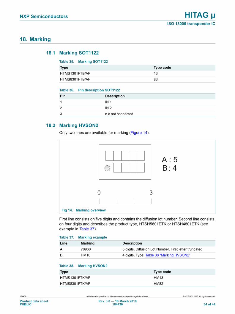
18.2 Marking HVSON2Only two lines are available for marking (Figure 14).
First line consists on five digits and contains the diffusion lot number. Second line consists on four digits and describes the product type, HTSH5601ETK or HTSH4801ETK (see example in Table 37).
Table 35. Marking SOT1122Type Type codeHTMS1301FTB/AF 13
HTMS8301FTB/AF 83
Table 36. Pin description SOT1122Pin Description1 IN 1
2 IN 2
3 n.c not connected
Fig 14. Marking overview
Table 37. Marking exampleLine Marking DescriptionA 70960 5 digits, Diffusion Lot Number, First letter truncated
B HM10 4 digits, Type: Table 38 “Marking HVSON2”
Table 38. Marking HVSON2Type Type codeHTMS1301FTK/AF HM13
HTMS8301FTK/AF HM82
0 3
A : 5B : 4
184430 All information provided in this document is subject to legal disclaimers. © NXP B.V. 2010. All rights reserved.
Product data sheetPUBLIC
Rev. 3.0 — 18 March 2010184430 34 of 44

NXP Semiconductors HITAG µISO 18000 transponder IC
19. Package outline
Fig 15. Package outline SOT1122
ReferencesOutlineversion
Europeanprojection
Issue dateIEC JEDEC JEITA
sot1122
Unit
mmaxnommin
0.50 0.040.55 0.425
0.300.250.22
0.350.300.27
A(1)
mensions
tesDimension A is including plating thickness.Can be visible in some manufacturing processes.
A1 D
1.501.451.40
1.051.000.95
E e e1
0.550.500.47
0.450.400.37
b b1 L L1
D
E
e1
e
A1
b1
L1
L
e1
0 1 2 mm
scale
3
1
2
b
4×(2)
4×(2)
A
pin 1 indication
type code
terminal 1index area
184430 All information provided in this document is subject to legal disclaimers. © NXP B.V. 2010. All rights reserved.
Product data sheetPUBLIC
Rev. 3.0 — 18 March 2010184430 35 of 44

NXP Semiconductors HITAG µISO 18000 transponder IC
Fig 16. Package outline HVSON2
REFERENCESOUTLINEVERSION
EUROPEANPROJECTION
ISSUE DATEIEC JEDEC JEITA
SOT899-1
SOT899-1
05-02-2505-05-09
Note1. Plastic or metal protrusions of 0.75 mm maximum per side are not included
UNIT Amax
mm 1 0.050
2.11.9
1.351.05
3.12.9
1.351.05
0.50.3
A1
DIMENSIONS (mm are the original dimensions)
HVSON2: plastic thermal enhanced very thin small outline package; no leads;2 terminals; body 3 × 2 × 0.85 mm
D
0.90.7
b Dh E Eh e
2.5
L y1
0.1
v
0.1
w
0.05
y
0.05
0 1 2 mm
scale
C
yCy1
X
detail X
A
A1
B AD
E
terminal 1index area
b
e
AC B∅ v M
C∅ w M
Dh
1
2
L
Eh
terminal 1index area
184430 All information provided in this document is subject to legal disclaimers. © NXP B.V. 2010. All rights reserved.
Product data sheetPUBLIC
Rev. 3.0 — 18 March 2010184430 36 of 44

NXP Semiconductors HITAG µISO 18000 transponder IC
20. Abbreviations
Table 39. AbbreviationsAbbreviation DefinitionAC Anticollision Code
AFI Application Family Identifier
ASK Amplitude Shift Keying
BC Bi-phase Code
BPLC Binary Pulse Length Coding
CRC Cyclic Redundancy Check
DSFID Data Storage Format Identifier
EEPROM Electrically Erasable Programmable Memory
EOF End Of Frame
ICR Integrated Circuit Reference number
LSB Least Significant Bit
LSByte Least Significant Byte
m Modulation Index
MC Manchester Code
MFC integrated circuit Manufacturer Code
MSB Most Significant Bit
MSByte Most Significant Byte
MSN Manufacturer Serial Number
NA No Access
NOB Number Of Block
NOP Number Of Pages
NOS Number Of Slots
NSS Number Of Sensors
OTP One Time Programmable
PID Product Identifier
PWD Password
RFU Reserved for Future Use
RND Random Number
RO Read Only
RTF Reader Talks First
R/W Read/Write
RWD Read/Write Device
SOF Start of Frame
UII Unique Item Identifier
184430 All information provided in this document is subject to legal disclaimers. © NXP B.V. 2010. All rights reserved.
Product data sheetPUBLIC
Rev. 3.0 — 18 March 2010184430 37 of 44

NXP Semiconductors HITAG µISO 18000 transponder IC
21. References
[1] Application note — AN10214, HITAG Coil Design Guide, Transponder IC BL-ID Doc.No.: 0814**1
[2] General specification for 8” wafer on UV-tape with electronic fail die marking — Delivery type description, BL-ID Doc.No.: 1093**1
1. ** ... document version number
184430 All information provided in this document is subject to legal disclaimers. © NXP B.V. 2010. All rights reserved.
Product data sheetPUBLIC
Rev. 3.0 — 18 March 2010184430 38 of 44

NXP Semiconductors HITAG µISO 18000 transponder IC
22. Revision history
Table 40: Revision historyDocument ID Release date Data sheet status Change notice Supersedes184430 20100318 Product data sheet - -
184430 All information provided in this document is subject to legal disclaimers. © NXP B.V. 2010. All rights reserved.
Product data sheetPUBLIC
Rev. 3.0 — 18 March 2010184430 39 of 44

NXP Semiconductors HITAG µISO 18000 transponder IC
23. Legal information
23.1 Data sheet status
[1] Please consult the most recently issued document before initiating or completing a design.
[2] The term ‘short data sheet’ is explained in section “Definitions”.
[3] The product status of device(s) described in this document may have changed since this document was published and may differ in case of multiple devices. The latest product status information is available on the Internet at URL http://www.nxp.com.
23.2 DefinitionsDraft — The document is a draft version only. The content is still under internal review and subject to formal approval, which may result in modifications or additions. NXP Semiconductors does not give any representations or warranties as to the accuracy or completeness of information included herein and shall have no liability for the consequences of use of such information.
Short data sheet — A short data sheet is an extract from a full data sheet with the same product type number(s) and title. A short data sheet is intended for quick reference only and should not be relied upon to contain detailed and full information. For detailed and full information see the relevant full data sheet, which is available on request via the local NXP Semiconductors sales office. In case of any inconsistency or conflict with the short data sheet, the full data sheet shall prevail.
Product specification — The information and data provided in a Product data sheet shall define the specification of the product as agreed between NXP Semiconductors and its customer, unless NXP Semiconductors and customer have explicitly agreed otherwise in writing. In no event however, shall an agreement be valid in which the NXP Semiconductors product is deemed to offer functions and qualities beyond those described in the Product data sheet.
23.3 DisclaimersLimited warranty and liability — Information in this document is believed to be accurate and reliable. However, NXP Semiconductors does not give any representations or warranties, expressed or implied, as to the accuracy or completeness of such information and shall have no liability for the consequences of use of such information.
In no event shall NXP Semiconductors be liable for any indirect, incidental, punitive, special or consequential damages (including - without limitation - lost profits, lost savings, business interruption, costs related to the removal or replacement of any products or rework charges) whether or not such damages are based on tort (including negligence), warranty, breach of contract or any other legal theory.
Notwithstanding any damages that customer might incur for any reason whatsoever, NXP Semiconductors’ aggregate and cumulative liability towards customer for the products described herein shall be limited in accordance with the Terms and conditions of commercial sale of NXP Semiconductors.
Right to make changes — NXP Semiconductors reserves the right to make changes to information published in this document, including without limitation specifications and product descriptions, at any time and without notice. This document supersedes and replaces all information supplied prior to the publication hereof.
Suitability for use — NXP Semiconductors products are not designed, authorized or warranted to be suitable for use in medical, military, aircraft, space or life support equipment, nor in applications where failure or
malfunction of an NXP Semiconductors product can reasonably be expected to result in personal injury, death or severe property or environmental damage. NXP Semiconductors accepts no liability for inclusion and/or use of NXP Semiconductors products in such equipment or applications and therefore such inclusion and/or use is at the customer’s own risk.
Applications — Applications that are described herein for any of these products are for illustrative purposes only. NXP Semiconductors makes no representation or warranty that such applications will be suitable for the specified use without further testing or modification.
NXP Semiconductors does not accept any liability related to any default, damage, costs or problem which is based on a weakness or default in the customer application/use or the application/use of customer’s third party customer(s) (hereinafter both referred to as “Application”). It is customer’s sole responsibility to check whether the NXP Semiconductors product is suitable and fit for the Application planned. Customer has to do all necessary testing for the Application in order to avoid a default of the Application and the product. NXP Semiconductors does not accept any liability in this respect.
Limiting values — Stress above one or more limiting values (as defined in the Absolute Maximum Ratings System of IEC 60134) will cause permanent damage to the device. Limiting values are stress ratings only and (proper) operation of the device at these or any other conditions above those given in the Recommended operating conditions section (if present) or the Characteristics sections of this document is not warranted. Constant or repeated exposure to limiting values will permanently and irreversibly affect the quality and reliability of the device.
Terms and conditions of commercial sale — NXP Semiconductors products are sold subject to the general terms and conditions of commercial sale, as published at http://www.nxp.com/profile/terms, unless otherwise agreed in a valid written individual agreement. In case an individual agreement is concluded only the terms and conditions of the respective agreement shall apply. NXP Semiconductors hereby expressly objects to applying the customer’s general terms and conditions with regard to the purchase of NXP Semiconductors products by customer.
No offer to sell or license — Nothing in this document may be interpreted or construed as an offer to sell products that is open for acceptance or the grant, conveyance or implication of any license under any copyrights, patents or other industrial or intellectual property rights.
Export control — This document as well as the item(s) described herein may be subject to export control regulations. Export might require a prior authorization from national authorities.
Quick reference data — The Quick reference data is an extract of the product data given in the Limiting values and Characteristics sections of this document, and as such is not complete, exhaustive or legally binding.
Non-automotive qualified products — Unless this data sheet expressly states that this specific NXP Semiconductors product is automotive qualified, the product is not suitable for automotive use. It is neither qualified nor tested in accordance with automotive testing or application requirements. NXP Semiconductors accepts no liability for inclusion and/or use of non-automotive qualified products in automotive equipment or applications.
Document status[1][2] Product status[3] Definition
Objective [short] data sheet Development This document contains data from the objective specification for product development.
Preliminary [short] data sheet Qualification This document contains data from the preliminary specification.
Product [short] data sheet Production This document contains the product specification.
184430 All information provided in this document is subject to legal disclaimers. © NXP B.V. 2010. All rights reserved.
Product data sheetPUBLIC
Rev. 3.0 — 18 March 2010184430 40 of 44

NXP Semiconductors HITAG µISO 18000 transponder IC
In the event that customer uses the product for design-in and use in automotive applications to automotive specifications and standards, customer (a) shall use the product without NXP Semiconductors’ warranty of the product for such automotive applications, use and specifications, and (b) whenever customer uses the product for automotive applications beyond NXP Semiconductors’ specifications such use shall be solely at customer’s own risk, and (c) customer fully indemnifies NXP Semiconductors for any liability, damages or failed product claims resulting from customer design and use of the product for automotive applications beyond NXP Semiconductors’ standard warranty and NXP Semiconductors’ product specifications.
23.4 Licenses
23.5 TrademarksNotice: All referenced brands, product names, service names and trademarks are the property of their respective owners.
HITAG — is a trademark of NXP B.V.
24. Contact information
For more information, please visit: http://www.nxp.com
For sales office addresses, please send an email to: [email protected]
ICs with HITAG functionality
NXP Semiconductors owns a worldwide perpetual license for the patents US 5214409, US 5499017, US 5235326 and for any foreign counterparts or equivalents of these patents. The license is granted for the Field-of-Use covering: (a) all non-animal applications, and (b) any application for animals raised for human consumption (including but not limited to dairy animals), including without limitation livestock and fish.
Please note that the license does not include rights outside the specified Field-of-Use, and that NXP Semiconductors does not provide indemnity for the foregoing patents outside the Field-of-Use.
184430 All information provided in this document is subject to legal disclaimers. © NXP B.V. 2010. All rights reserved.
Product data sheetPUBLIC
Rev. 3.0 — 18 March 2010184430 41 of 44

NXP Semiconductors HITAG µISO 18000 transponder IC
25. Tables
Table 1. Ordering information. . . . . . . . . . . . . . . . . . . . . .2Table 2. HITAG µ ISO 18000 - Mega bumps dimensions.4Table 3. Memory organization . . . . . . . . . . . . . . . . . . . . .7Table 4. User configuration block to Byte0. . . . . . . . . . . .8Table 5. Modulation coding times[1][2] . . . . . . . . . . . . . . . .9Table 6. Data coding times [1] . . . . . . . . . . . . . . . . . . . . .10Table 7. Overview timing parameters [1] . . . . . . . . . . . . .16Table 8. Reader - Transponder IC transmission [1][2] . . .20Table 9. Transponder IC - Reader transmission [1][2] . . .20Table 10. Command Flags . . . . . . . . . . . . . . . . . . . . . . . .21Table 11. Command Flags - Bit order. . . . . . . . . . . . . . . .21Table 12. Meaning of ADR and SEL flag . . . . . . . . . . . . .21Table 13. Response format in error case . . . . . . . . . . . . .22Table 14. INVENTORY - Request format (00h) . . . . . . . .23Table 15. Response to a successful INVENTORY request
[1][2] . . . . . . . . . . . . . . . . . . . . . . . . . . . . . . . . . .23Table 16. STAY QUIET - request format(01h) . . . . . . . . .23Table 17. READ UII - request format (02h) . . . . . . . . . . .24Table 18. Response to a successful READ UII request .24Table 19. READ MULTIPLE BLOCKS - request format
(12h) . . . . . . . . . . . . . . . . . . . . . . . . . . . . . . . .25Table 20. Response to a successful READ MULTIPLE
BLOCKS request . . . . . . . . . . . . . . . . . . . . . . .25Table 21. READ MULTIPLE BLOCKS - request format
(12h) . . . . . . . . . . . . . . . . . . . . . . . . . . . . . . . . .26
Table 22. READ MULTIPLE BLOCKS in INVENTORY mode Response format [1] . . . . . . . . . . . . . . . . . . . . . 26
Table 23. WRITE SINGLE BLOCK - request format(14h). . . . . . . . . . . . . . . . . . . . . . . . . . . . . . . . . 27
Table 24. Response to a successful WRITE SINGLE BLOCK request . . . . . . . . . . . . . . . . . . . . . . . . 27
Table 25. LOCK BLOCK - request format (16h) . . . . . . . 28Table 26. Response to a successful LOCK BLOCK
request . . . . . . . . . . . . . . . . . . . . . . . . . . . . . . . 28Table 27. SELECT - request format (18h) . . . . . . . . . . . . 29Table 28. Response to a successful SELECT request . . 29Table 29. GET SYSTEM INFORMATION - request format
(17h). . . . . . . . . . . . . . . . . . . . . . . . . . . . . . . . . 30Table 30. GET SYSTEM INFORMATION - response
format. . . . . . . . . . . . . . . . . . . . . . . . . . . . . . . . 30Table 31. LOGIN - request format . . . . . . . . . . . . . . . . . . 31Table 32. Response to a successful LOGIN request. . . . 31Table 33. Limiting values[1][2] . . . . . . . . . . . . . . . . . . . . . . 33Table 34. Characteristics . . . . . . . . . . . . . . . . . . . . . . . . . 33Table 35. Marking SOT1122 . . . . . . . . . . . . . . . . . . . . . . 34Table 36. Pin description SOT1122 . . . . . . . . . . . . . . . . . 34Table 37. Marking example . . . . . . . . . . . . . . . . . . . . . . . 34Table 38. Marking HVSON2 . . . . . . . . . . . . . . . . . . . . . . 34Table 39. Abbreviations . . . . . . . . . . . . . . . . . . . . . . . . . . 37Table 40: Revision history . . . . . . . . . . . . . . . . . . . . . . . . 39
26. Figures
Fig 1. Block diagram of HITAG µ ISO 18000 transponder IC . . . . . . . . . . . . . . . . . . . . . . . . . . . . . . . . . . . . . .3
Fig 2. HITAG µ ISO 1800 - Mega bumps bondpad locations. . . . . . . . . . . . . . . . . . . . . . . . . . . . . . . . .4
Fig 3. Modulation details of data transmission from RWD to HITAG µ transponder IC . . . . . . . . . . . . . . . . . .9
Fig 4. Reader to HITAG µ ISO 18000 transponder IC: Pulse Interval Encoding . . . . . . . . . . . . . . . . . . . .10
Fig 5. Start of frame pattern . . . . . . . . . . . . . . . . . . . . . . 11Fig 6. End of frame pattern . . . . . . . . . . . . . . . . . . . . . . 11Fig 7. HITAG µ ISO 18000 transponder IC - Load
modulation coding . . . . . . . . . . . . . . . . . . . . . . . .12Fig 8. Start of fame pattern . . . . . . . . . . . . . . . . . . . . . .13Fig 9. General protocol timing diagram . . . . . . . . . . . . .14Fig 10. Protocol timing diagram without HITAG µ ISO 18000
transponder IC response . . . . . . . . . . . . . . . . . . .16Fig 11. State diagram of HITAG µ ISO18000 transponder
ICs . . . . . . . . . . . . . . . . . . . . . . . . . . . . . . . . . . . .18Fig 12. HITAG µ ISO 18000 transponder IC response - in
case of no error . . . . . . . . . . . . . . . . . . . . . . . . . .22Fig 13. HITAG µ ISO 18000 transponder IC response - in
error case. . . . . . . . . . . . . . . . . . . . . . . . . . . . . . .22Fig 14. Marking overview. . . . . . . . . . . . . . . . . . . . . . . . .34Fig 15. Package outline SOT1122 . . . . . . . . . . . . . . . . . .35Fig 16. Package outline HVSON2 . . . . . . . . . . . . . . . . . .36
184430 All information provided in this document is subject to legal disclaimers. © NXP B.V. 2010. All rights reserved.
Product data sheetPUBLIC
Rev. 3.0 — 18 March 2010184430 42 of 44

NXP Semiconductors HITAG µISO 18000 transponder IC
27. Contents
1 General description . . . . . . . . . . . . . . . . . . . . . . 12 Features and benefits . . . . . . . . . . . . . . . . . . . . 12.1 Features . . . . . . . . . . . . . . . . . . . . . . . . . . . . . . 12.2 Protocol . . . . . . . . . . . . . . . . . . . . . . . . . . . . . . 12.3 Memory. . . . . . . . . . . . . . . . . . . . . . . . . . . . . . . 22.4 Supported standards . . . . . . . . . . . . . . . . . . . . 22.5 Security features. . . . . . . . . . . . . . . . . . . . . . . . 22.6 Delivery types . . . . . . . . . . . . . . . . . . . . . . . . . . 23 Applications . . . . . . . . . . . . . . . . . . . . . . . . . . . . 24 Ordering information. . . . . . . . . . . . . . . . . . . . . 25 Block diagram . . . . . . . . . . . . . . . . . . . . . . . . . . 36 Pinning information. . . . . . . . . . . . . . . . . . . . . . 47 Mechanical specification . . . . . . . . . . . . . . . . . 57.1 Wafer specification . . . . . . . . . . . . . . . . . . . . . . 57.1.1 Wafer . . . . . . . . . . . . . . . . . . . . . . . . . . . . . . . . 57.1.2 Wafer backside . . . . . . . . . . . . . . . . . . . . . . . . . 57.1.3 Chip dimensions . . . . . . . . . . . . . . . . . . . . . . . . 57.1.4 Passivation on front . . . . . . . . . . . . . . . . . . . . . 57.1.5 Au bump . . . . . . . . . . . . . . . . . . . . . . . . . . . . . . 67.1.6 Fail die identification . . . . . . . . . . . . . . . . . . . . 67.1.7 Map file distribution. . . . . . . . . . . . . . . . . . . . . . 68 Functional description . . . . . . . . . . . . . . . . . . . 78.1 Memory organization . . . . . . . . . . . . . . . . . . . . 78.1.1 Memory organization . . . . . . . . . . . . . . . . . . . . 78.2 Memory configuration . . . . . . . . . . . . . . . . . . . . 89 General requirements . . . . . . . . . . . . . . . . . . . . 810 HITAG m ISO 18000 transponder IC air
interface . . . . . . . . . . . . . . . . . . . . . . . . . . . . . . . 910.1 Downlink communication signal interface - RWD
to HITAG m ISO 18000 transponder IC . . . . . . 910.1.1 Modulation parameters . . . . . . . . . . . . . . . . . . . 910.1.2 Data rate and data coding . . . . . . . . . . . . . . . 1010.1.3 RWD - Start of frame pattern . . . . . . . . . . . . . 1110.1.4 RWD - End of frame pattern . . . . . . . . . . . . . . 1110.2 Communication signal interface -
HITAG µ ISO 18000 transponder IC to RWD . 1210.2.1 Data rate and data coding . . . . . . . . . . . . . . . 1210.2.2 Start of frame pattern . . . . . . . . . . . . . . . . . . . 1310.2.3 End of frame pattern . . . . . . . . . . . . . . . . . . . . 1311 General protocol timing specification . . . . . . 1411.1 Waiting time before transmitting a response after
an EOF from the RWD . . . . . . . . . . . . . . . . . . 1411.2 RWD waiting time before sending a subsequent
request . . . . . . . . . . . . . . . . . . . . . . . . . . . . . . 1511.3 RWD waiting time before switching to next
inventory slot . . . . . . . . . . . . . . . . . . . . . . . . . 15
11.3.1 RWD started to receive one or more HITAG µ ISO 18000 transponder IC responses . . . . . . 15
11.3.2 RWD receives no HITAG µ ISO 18000 transponder IC response . . . . . . . . . . . . . . . . 16
12 State diagram. . . . . . . . . . . . . . . . . . . . . . . . . . 1712.1 General description of states . . . . . . . . . . . . . 1712.2 State diagram HITAG µ ISO 18000 . . . . . . . . 1813 Modes. . . . . . . . . . . . . . . . . . . . . . . . . . . . . . . . 1913.1 Anticollision . . . . . . . . . . . . . . . . . . . . . . . . . . 1913.1.1 Anticollision with 1 slot . . . . . . . . . . . . . . . . . . 1913.1.2 Anticollision with 16 slots . . . . . . . . . . . . . . . . 1914 Command set . . . . . . . . . . . . . . . . . . . . . . . . . 2014.1 Flags . . . . . . . . . . . . . . . . . . . . . . . . . . . . . . . 2114.2 Error handling . . . . . . . . . . . . . . . . . . . . . . . . 2214.3 INVENTORY . . . . . . . . . . . . . . . . . . . . . . . . . 2314.4 STAY QUIET . . . . . . . . . . . . . . . . . . . . . . . . . 2314.5 READ UII . . . . . . . . . . . . . . . . . . . . . . . . . . . 2414.6 READ MULTIPLE BLOCK . . . . . . . . . . . . . . . 2514.6.1 READ MULTIPLE BLOCKS in INVENTORY
mode . . . . . . . . . . . . . . . . . . . . . . . . . . . . . . . 2614.7 WRITE SINGLE BLOCK . . . . . . . . . . . . . . . . 2714.8 LOCK BLOCK . . . . . . . . . . . . . . . . . . . . . . . . 2814.9 SELECT. . . . . . . . . . . . . . . . . . . . . . . . . . . . . 2914.10 GET SYSTEM INFORMATION . . . . . . . . . . . 3014.11 LOGIN . . . . . . . . . . . . . . . . . . . . . . . . . . . . . . 3115 Data integrity/calculation of CRC . . . . . . . . . 3215.1 Data transmission: RWD to HITAG µ ISO 18000
transponder IC . . . . . . . . . . . . . . . . . . . . . . . . 3215.2 Data transmission: HITAG µ ISO 18000
transponder IC to RWD . . . . . . . . . . . . . . . . . 3216 Limiting values . . . . . . . . . . . . . . . . . . . . . . . . 3317 Characteristics . . . . . . . . . . . . . . . . . . . . . . . . 3318 Marking . . . . . . . . . . . . . . . . . . . . . . . . . . . . . . 3418.1 Marking SOT1122 . . . . . . . . . . . . . . . . . . . . . 3418.2 Marking HVSON2 . . . . . . . . . . . . . . . . . . . . . 3419 Package outline. . . . . . . . . . . . . . . . . . . . . . . . 3520 Abbreviations . . . . . . . . . . . . . . . . . . . . . . . . . 3721 References. . . . . . . . . . . . . . . . . . . . . . . . . . . . 3822 Revision history . . . . . . . . . . . . . . . . . . . . . . . 3923 Legal information . . . . . . . . . . . . . . . . . . . . . . 4023.1 Data sheet status . . . . . . . . . . . . . . . . . . . . . . 4023.2 Definitions . . . . . . . . . . . . . . . . . . . . . . . . . . . 4023.3 Disclaimers . . . . . . . . . . . . . . . . . . . . . . . . . . 4023.4 Licenses. . . . . . . . . . . . . . . . . . . . . . . . . . . . . 4123.5 Trademarks . . . . . . . . . . . . . . . . . . . . . . . . . . 41
184430 All information provided in this document is subject to legal disclaimers. © NXP B.V. 2010. All rights reserved.
Product data sheetPUBLIC
Rev. 3.0 — 18 March 2010184430 43 of 44
continued >>

NXP Semiconductors HITAG µISO 18000 transponder IC
24 Contact information. . . . . . . . . . . . . . . . . . . . . 4125 Tables . . . . . . . . . . . . . . . . . . . . . . . . . . . . . . . . 4226 Figures . . . . . . . . . . . . . . . . . . . . . . . . . . . . . . . 4227 Contents . . . . . . . . . . . . . . . . . . . . . . . . . . . . . . 43
© NXP B.V. 2010. All rights reserved.For more information, please visit: http://www.nxp.comFor sales office addresses, please send an email to: [email protected]
Date of release: 18 March 2010184430
Please be aware that important notices concerning this document and the product(s)described herein, have been included in section ‘Legal information’.
Related Documents