TN90002 H-bridge motor controller design using Nexperia discrete semiconductors and logic ICs Rev. 3 — 14 February 2020 Technical note Document information Information Content Keywords H-bridge, MOSFET, motor controller Abstract An example of a H-bridge motor controller designed with Nexperia discrete and Nexperia logic IC components.

Welcome message from author
This document is posted to help you gain knowledge. Please leave a comment to let me know what you think about it! Share it to your friends and learn new things together.
Transcript
TN90002H-bridge motor controller design using Nexperia discretesemiconductors and logic ICsRev. 3 — 14 February 2020 Technical note
Document informationInformation Content
Keywords H-bridge, MOSFET, motor controller
Abstract An example of a H-bridge motor controller designed with Nexperia discrete and Nexperia logic ICcomponents.
Nexperia TN90002H-bridge motor controller design using Nexperia discrete semiconductors and logic ICs
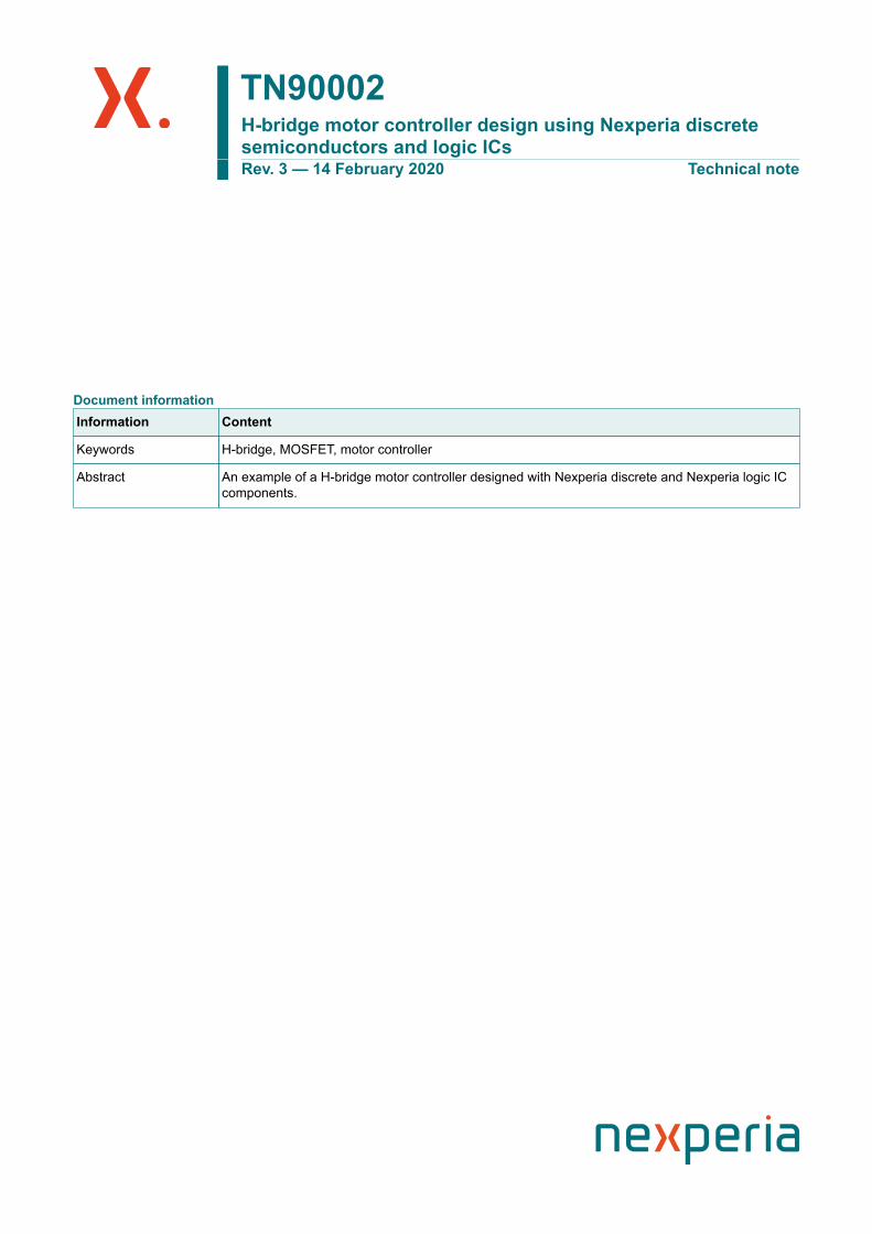
1. IntroductionThis technical note demonstrates a H-bridge motor controller PCB, built using Nexperia discretesemiconductors and logic ICs.
The H-bridge circuit is a full bridge DC-to-DC converter allowing operation of a brushed DC motor(48 V max, 12 V min, 5 A max). The key feature of this design is that all electronic functions aredesigned with Nexperia discrete and logic IC components (low cost, no micro-controller or softwareneeded).
M
Q1 Q2
Q3 Q4
+V +V
aaa-030956
Fig. 1. Simplified MOSFET H-bridge motor control
The left MOSFETs of the full bridge (Q1 and Q3 in the simplified diagram above) are the switchingMOSFETs (see the PCB top view in Fig. 26), the right MOSFETs (Q2 and Q4 in the simplifieddiagram above) select the motor rotation direction:
• right high side MOSFET fully ON = Forward• right low side MOSFET fully ON = Reverse
A switch selects the motor rotation direction.
Jumpers select one of 3 switching frequencies: 7.8 kHz, 15.6 kHz or 31.3 kHz.
Two tactile push buttons allow the duty cycle (motor speed) to be increased or decreased. Thereare 8 steps from 0 to 100% duty cycle. A current limitation protection avoids over current in themotor and MOSFETs (set at approximately 6.5 A).
This H-bridge motor controller PCB allows the user to choose between 3 Nexperia MOSFETpackages (LFPAK33, LFPAK56D or LFPAK56), jumpers are used to connect the MOSFETs chosenby the user.
This technical note describes each of the main functions used in the design.
TN90002 All information provided in this document is subject to legal disclaimers. © Nexperia B.V. 2020. All rights reserved
Technical note Rev. 3 — 14 February 2020 2 / 38
Nexperia TN90002H-bridge motor controller design using Nexperia discrete semiconductors and logic ICs
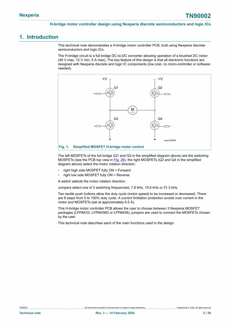
2. Block diagram and system functionality
Over-current
Detection
aaa-030969
Clock PWM DrivingCircuitry H-bridge Motor
PowerSupply
Fig. 2. H-bridge motor controller block diagram
2.1. Subsystems overview1. Power Supply
• Accepts 12 V to 48 V DC input• Transient overvoltage protection• Reverse polarity protection• Buck converter (12 V)• Linear regulator (5 V) for logic devices
2. Clock and duty cycle generator• 4 MHz crystal oscillator and frequency divider to create 3 different switching frequencies• Duty cycle sets by push button inputs to select the duty cycle (0% to 100%)• 62.5 kHz output is used to supply the charge pump on the driving circuitry block
3. PWM• Reset function to activate other function when VCC 5 V supply is stable• Dead-time function and PWM enable (over current protection disabling)• Level shifter• Direction selection
4. Driver circuit• High-side and low-side drivers to drive 4 MOSFETs of the full bridge• Charge pump to supply the high-side MOSFETs
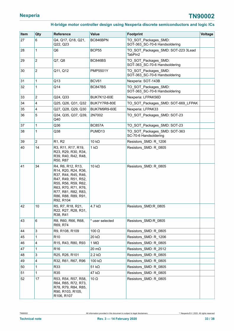
5. H-bridge• Reservoir and decoupling capacitors• Snubber on the left MOSFETs (switching MOSFETs)• Jumper to connect the selected MOSFETs• Gate drive resistors• Low-side current measurement
6. Overcurrent detection• Comparator, with voltage reference setting current limit• PWM reset function reactivating PWM if fault disappears
TN90002 All information provided in this document is subject to legal disclaimers. © Nexperia B.V. 2020. All rights reserved
Technical note Rev. 3 — 14 February 2020 3 / 38
Nexperia TN90002H-bridge motor controller design using Nexperia discrete semiconductors and logic ICs
3. Subsystem descriptions
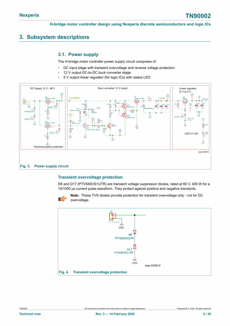
3.1. Power supplyThe H-bridge motor controller power supply circuit comprises of:
• DC input stage with transient overvoltage and reverse voltage protection• 12 V output DC-to-DC buck converter stage• 5 V output linear regulator (for logic ICs) with status LED
Reverse polarity protection
Buck converter 12 V outputDC Supply 12 V - 48 V Linear regulator
, ,
, ,
LED 5 V OK
12 V to 5 V
aaa-030910
Fig. 3. Power supply circuit
Transient overvoltage protectionD8 and D17 (PTVS60VS1UTR) are transient voltage suppressor diodes, rated at 60 V, 400 W for a10/1000 μs current pulse waveform. They protect against positive and negative transients.
Note: These TVS diodes provide protection for transient overvoltage only - not for DCovervoltage.
aaa-030914
Fig. 4. Transient overvoltage protection
TN90002 All information provided in this document is subject to legal disclaimers. © Nexperia B.V. 2020. All rights reserved
Technical note Rev. 3 — 14 February 2020 4 / 38
Nexperia TN90002H-bridge motor controller design using Nexperia discrete semiconductors and logic ICs
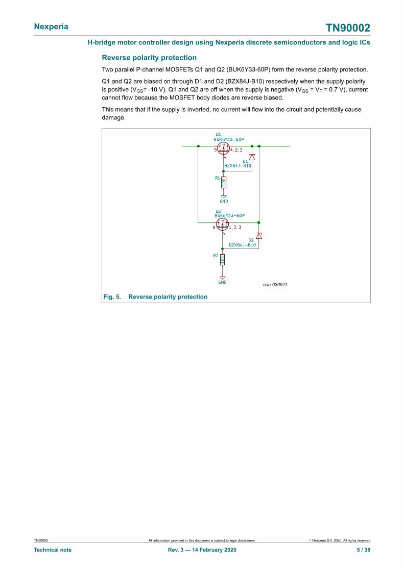
Reverse polarity protectionTwo parallel P-channel MOSFETs Q1 and Q2 (BUK6Y33-60P) form the reverse polarity protection.
Q1 and Q2 are biased on through D1 and D2 (BZX84J-B10) respectively when the supply polarityis positive (VGS= -10 V). Q1 and Q2 are off when the supply is negative (VGS = VF = 0.7 V), currentcannot flow because the MOSFET body diodes are reverse biased.
This means that if the supply is inverted, no current will flow into the circuit and potentially causedamage.
, ,
, ,
aaa-030911
Fig. 5. Reverse polarity protection
TN90002 All information provided in this document is subject to legal disclaimers. © Nexperia B.V. 2020. All rights reserved
Technical note Rev. 3 — 14 February 2020 5 / 38

Nexperia TN90002H-bridge motor controller design using Nexperia discrete semiconductors and logic ICs
Buck converter (12 V)The next stage is a switching regulator that outputs 12 V. To start the switching regulator a start-up circuit is used consisting of: Zener diode D18 (BZX84J-B5V6), R10, and C14. This provides a5 V supply for inverting Schmitt trigger U21 (74HC1G14) before VCC (5 V) is available through D19(BAS316). U21 can then start the switching regulation.
The buck converter consists of: Q5 (BUK6Y33-60P), Schottky diode D6 (PMEG10030ELP) andinductor L1. The output of the buck converter supplies the 12 V rail.
When the output of U21 is high it turns on Q5 via the NPN transistor Q3 (BC846) and the NPN/PNP dual transistor pair Q4 (BC846BPN). The voltage on node “V_12” will then increase. When“V_12” reaches 12 V, D3 ( BZX84J-B10) is conducting and there is enough voltage on U21 input toforce U21 output low. Then Q5 is switched off and the voltage at “V_12” decreases until U21 inputis low enough to restart a new cycle.
aaa-030912
Fig. 6. Buck converter
Linear regulator (5 V) for logic ICsA linear regulator comprising NPN transistor Q6 (BCP55), Zener diode D7 (BZX84J-B5V6) and R11provides a regulated VCC (5 V) rail for the logic ICs.
aaa-030913
Fig. 7. Linear regulator
TN90002 All information provided in this document is subject to legal disclaimers. © Nexperia B.V. 2020. All rights reserved
Technical note Rev. 3 — 14 February 2020 6 / 38
Nexperia TN90002H-bridge motor controller design using Nexperia discrete semiconductors and logic ICs
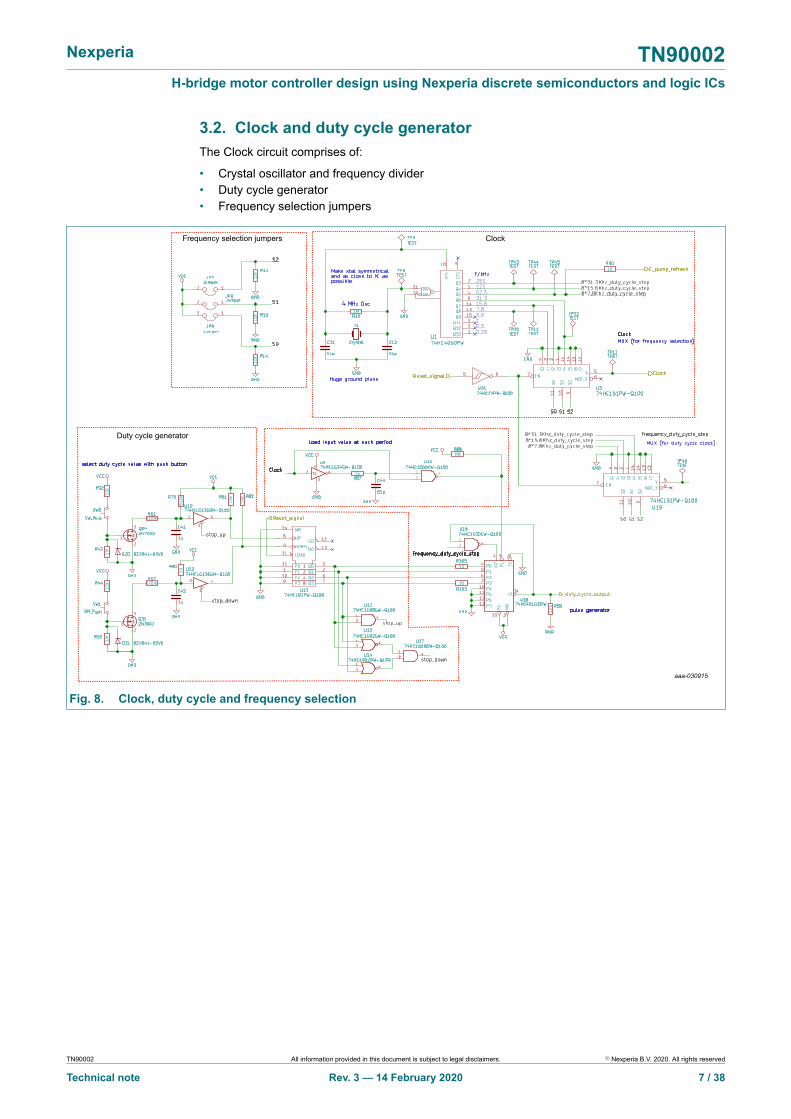
3.2. Clock and duty cycle generatorThe Clock circuit comprises of:
• Crystal oscillator and frequency divider• Duty cycle generator• Frequency selection jumpers
Duty cycle generator
Frequency selection jumpers Clock
aaa-030915
Fig. 8. Clock, duty cycle and frequency selection
TN90002 All information provided in this document is subject to legal disclaimers. © Nexperia B.V. 2020. All rights reserved
Technical note Rev. 3 — 14 February 2020 7 / 38

Nexperia TN90002H-bridge motor controller design using Nexperia discrete semiconductors and logic ICs
Crystal oscillator and frequency dividerA crystal oscillator is used for accuracy and stability. The oscillator frequency is 4 MHz.
U1 (74HCT4060) is a frequency divider, used to obtain different frequencies from the 4 MHz. Itprovides outputs at:
• 62.5 kHz to drive the charge pump circuit (see Fig. 19)• 31.3 kHz, 15.6 kHz and 7.8 kHz for the switching frequency (user selectable)
The switching frequency is selected by the multiplexer U3 (74HCT151) according to the jumpersettings of JP7, JP8 and JP9.
Note: Only one jumper should be fitted at the same time.
The switching frequency output is labeled “Clock”.
A reset signal enables both multiplexer U3 and U19 (see next section for U19 explanation) whenVCC is 5 V.
Frequency selection jumpers Clock
aaa-030937
Fig. 9. Oscillator and frequency divider
TN90002 All information provided in this document is subject to legal disclaimers. © Nexperia B.V. 2020. All rights reserved
Technical note Rev. 3 — 14 February 2020 8 / 38
Nexperia TN90002H-bridge motor controller design using Nexperia discrete semiconductors and logic ICs
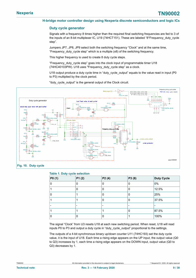
Duty cycle generatorSignals with a frequency 8 times higher than the required final switching frequencies are fed to 3 ofthe inputs of an 8-bit multiplexer IC, U19 (74HCT151). These are labeled “8*Frequency_duty_cyclestep”.
Jumpers JP7, JP8, JP9 select both the switching frequency “Clock” and at the same time,“Frequency_duty_cycle step” which is a multiple (x8) of the switching frequency.
This higher frequency is used to create 8 duty cycle steps.
“Frequency_duty_cycle step” goes into the clock input of programmable timer U18(74HC40103PW). U18 uses "Frequency_duty_cycle step” as a clock.
U18 output produce a duty cycle time in “duty_cycle_output” equals to the value read in input (P0to P3) multiplied by the clock period.
"duty_cycle_output” is the general output of the Clock circuit.
Duty cycle generator
aaa-030938
Fig. 10. Duty cycle
Table 1. Duty cycle selectionP0 (1) P1 (2) P2 (4) P3 (8) Duty Cycle
0 0 0 0 0%
1 0 0 0 12.5%
0 1 0 0 25%
1 1 0 0 37.5%
- - - - -
1 1 1 0 87.5%
0 0 0 1 100%
The signal “Clock” from U3 resets U18 at each new switching period. When reset, U18 will readinputs P0 to P3 and output a duty cycle in “duty_cycle_output” proportional to the settings.
The outputs of a 4-bit synchronous binary up/down counter U11 (74HC193) set the duty cyclevalue, it is the input of U18. Each time a rising edge appears on the UP input, the output value (Q0to Q3) increases by 1, each time a rising edge appears on the DOWN input, output value (Q0 toQ3) decreases by 1.
TN90002 All information provided in this document is subject to legal disclaimers. © Nexperia B.V. 2020. All rights reserved
Technical note Rev. 3 — 14 February 2020 9 / 38
Nexperia TN90002H-bridge motor controller design using Nexperia discrete semiconductors and logic ICs
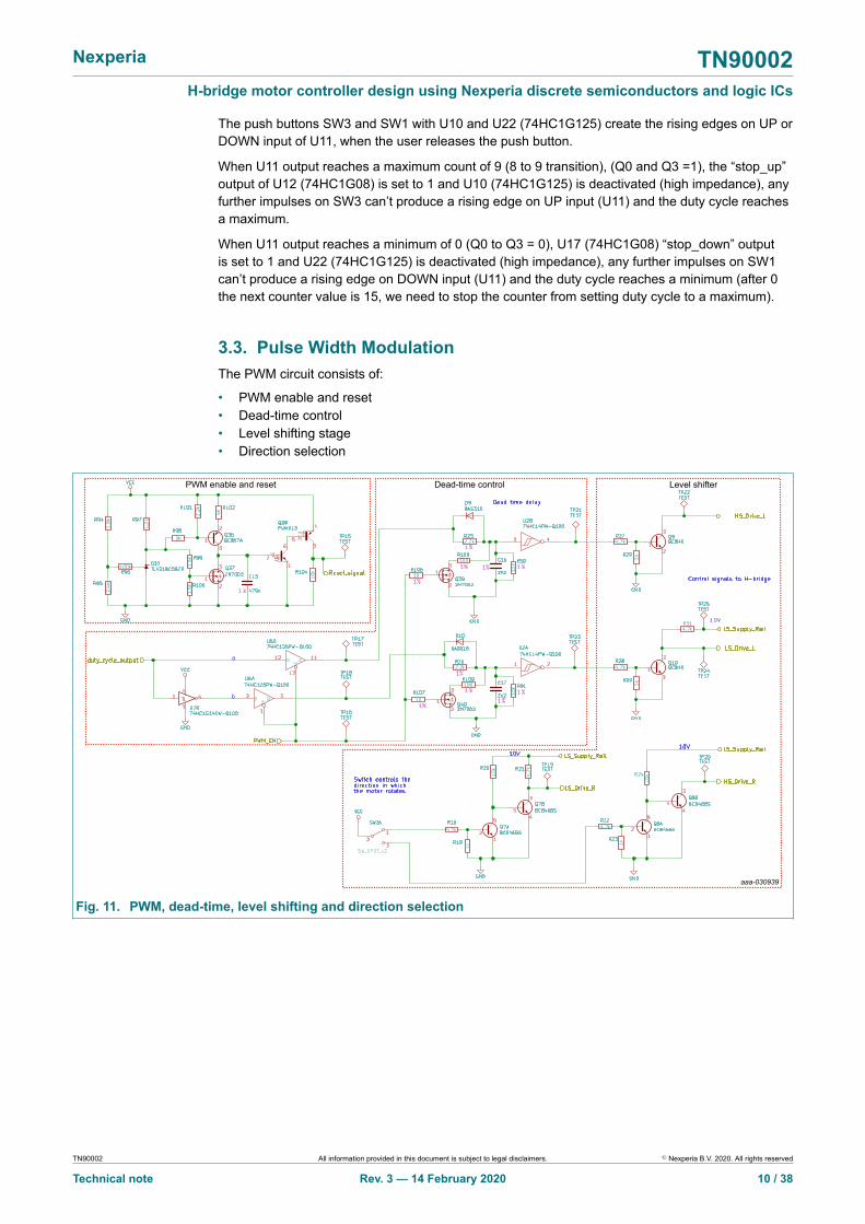
The push buttons SW3 and SW1 with U10 and U22 (74HC1G125) create the rising edges on UP orDOWN input of U11, when the user releases the push button.
When U11 output reaches a maximum count of 9 (8 to 9 transition), (Q0 and Q3 =1), the “stop_up”output of U12 (74HC1G08) is set to 1 and U10 (74HC1G125) is deactivated (high impedance), anyfurther impulses on SW3 can’t produce a rising edge on UP input (U11) and the duty cycle reachesa maximum.
When U11 output reaches a minimum of 0 (Q0 to Q3 = 0), U17 (74HC1G08) “stop_down” outputis set to 1 and U22 (74HC1G125) is deactivated (high impedance), any further impulses on SW1can’t produce a rising edge on DOWN input (U11) and the duty cycle reaches a minimum (after 0the next counter value is 15, we need to stop the counter from setting duty cycle to a maximum).
3.3. Pulse Width ModulationThe PWM circuit consists of:
• PWM enable and reset• Dead-time control• Level shifting stage• Direction selection
PWM enable and reset Dead-time control Level shifter
aaa-030939
Fig. 11. PWM, dead-time, level shifting and direction selection
TN90002 All information provided in this document is subject to legal disclaimers. © Nexperia B.V. 2020. All rights reserved
Technical note Rev. 3 — 14 February 2020 10 / 38
Nexperia TN90002H-bridge motor controller design using Nexperia discrete semiconductors and logic ICs
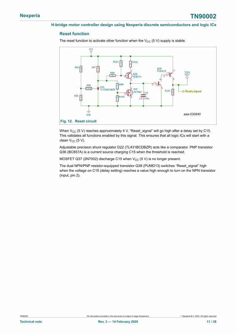
Reset functionThe reset function to activate other function when the VCC (5 V) supply is stable.
aaa-030940
Fig. 12. Reset circuit
When VCC (5 V) reaches approximately 4 V, “Reset_signal” will go high after a delay set by C15.This validates all functions enabled by this signal. This ensures that all logic ICs will start with aclean VCC (5 V).
Adjustable precision shunt regulator D22 (TL431BCDBZR) acts like a comparator. PNP transistorQ36 (BC857A) is a current source charging C15 when the threshold is reached.
MOSFET Q37 (2N7002) discharge C15 when VCC (5 V) is no longer present.
The dual NPN/PNP resistor-equipped transistor Q38 (PUMD13) switches “Reset_signal” highwhen the voltage on C15 (delay setting) reaches a value high enough to turn on the NPN transistor(input, pin 2).
TN90002 All information provided in this document is subject to legal disclaimers. © Nexperia B.V. 2020. All rights reserved
Technical note Rev. 3 — 14 February 2020 11 / 38
Nexperia TN90002H-bridge motor controller design using Nexperia discrete semiconductors and logic ICs
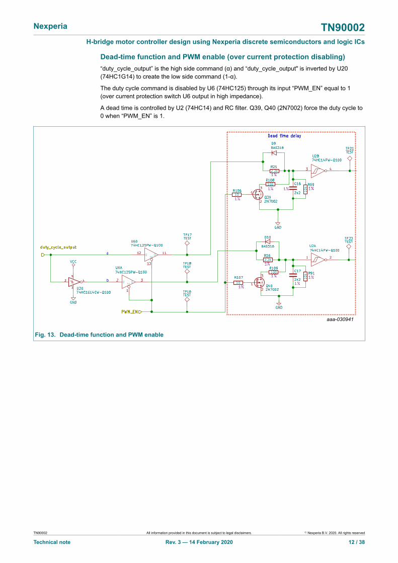
Dead-time function and PWM enable (over current protection disabling)“duty_cycle_output” is the high side command (α) and “duty_cycle_output" is inverted by U20(74HC1G14) to create the low side command (1-α).
The duty cycle command is disabled by U6 (74HC125) through its input “PWM_EN” equal to 1(over current protection switch U6 output in high impedance).
A dead time is controlled by U2 (74HC14) and RC filter. Q39, Q40 (2N7002) force the duty cycle to0 when “PWM_EN” is 1.
aaa-030941
Fig. 13. Dead-time function and PWM enable
TN90002 All information provided in this document is subject to legal disclaimers. © Nexperia B.V. 2020. All rights reserved
Technical note Rev. 3 — 14 February 2020 12 / 38
Nexperia TN90002H-bridge motor controller design using Nexperia discrete semiconductors and logic ICs
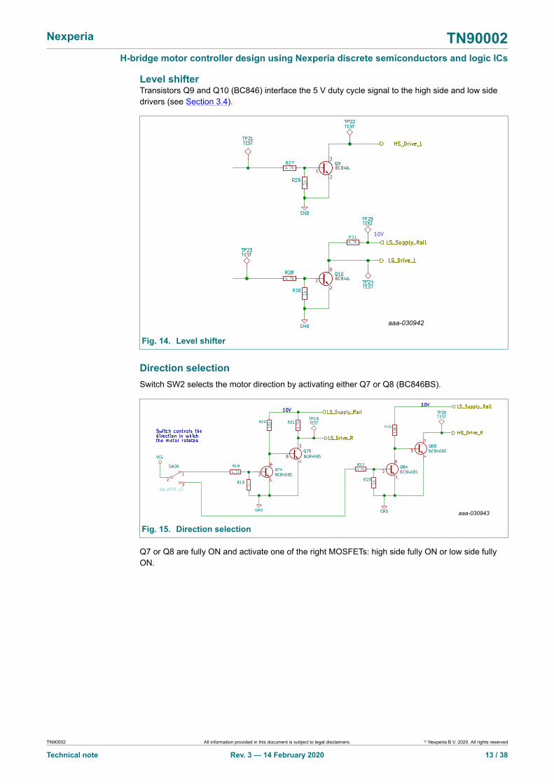
Level shifterTransistors Q9 and Q10 (BC846) interface the 5 V duty cycle signal to the high side and low sidedrivers (see Section 3.4).
aaa-030942
Fig. 14. Level shifter
Direction selectionSwitch SW2 selects the motor direction by activating either Q7 or Q8 (BC846BS).
aaa-030943
Fig. 15. Direction selection
Q7 or Q8 are fully ON and activate one of the right MOSFETs: high side fully ON or low side fullyON.
TN90002 All information provided in this document is subject to legal disclaimers. © Nexperia B.V. 2020. All rights reserved
Technical note Rev. 3 — 14 February 2020 13 / 38

Nexperia TN90002H-bridge motor controller design using Nexperia discrete semiconductors and logic ICs
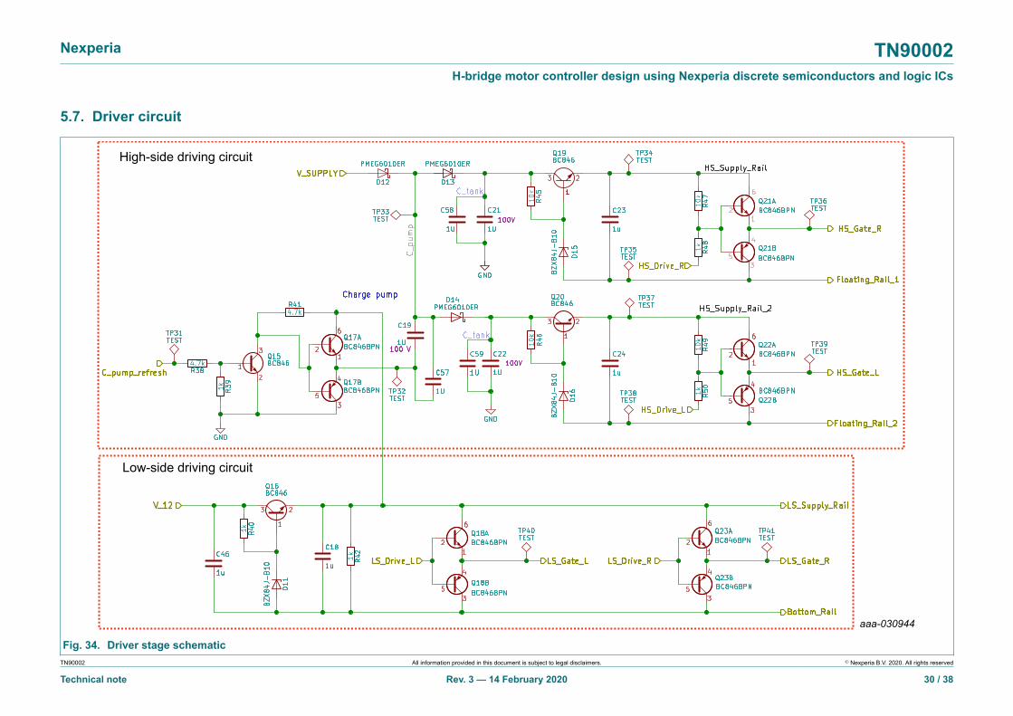
3.4. Drive circuitThe drive circuit comprises of high-side and low-side drivers to drive the 4 power MOSFETs thatform the full bridge.
High-side driving circuit
Low-side driving circuit
aaa-030944
Fig. 16. Driver circuit
TN90002 All information provided in this document is subject to legal disclaimers. © Nexperia B.V. 2020. All rights reserved
Technical note Rev. 3 — 14 February 2020 14 / 38

Nexperia TN90002H-bridge motor controller design using Nexperia discrete semiconductors and logic ICs
High-side and low-side driversTwo high side drivers supplied by the charge pump function and regulated at 9 V:
• Q19 (BC846), D15 (BZX84J-B10), C23, R45, Q21(BC846BPN) driven by “HS_Drive_R” for theright high side
• Q20 (BC846), D16(BZX84J-B10), C24, R46, Q22(BC846BPN) driven by “HS_Drive_L” for theleft high side
aaa-030945
Fig. 17. High side driver circuit
Two Low side drivers supplied by the 12 V from the buck converter and regulated at 9 V
• Q16 (BC846), D11(BZX84J-B10), C18, R40 for the supply:• Q18(BC846BPN) driven by “LS_Drive_L” for the left low side• Q23 (BC846BPN) driven by “LS_Drive_R” for the right low side
aaa-030946
Fig. 18. Low side driver circuit
TN90002 All information provided in this document is subject to legal disclaimers. © Nexperia B.V. 2020. All rights reserved
Technical note Rev. 3 — 14 February 2020 15 / 38
Nexperia TN90002H-bridge motor controller design using Nexperia discrete semiconductors and logic ICs
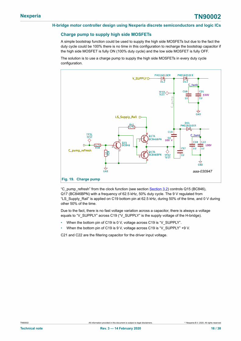
Charge pump to supply high side MOSFETsA simple bootstrap function could be used to supply the high side MOSFETs but due to the fact theduty cycle could be 100% there is no time in this configuration to recharge the bootstrap capacitor ifthe high side MOSFET is fully ON (100% duty cycle) and the low side MOSFET is fully OFF.
The solution is to use a charge pump to supply the high side MOSFETs in every duty cycleconfiguration.
aaa-030947
Fig. 19. Charge pump
“C_pump_refresh” from the clock function (see section Section 3.2) controls Q15 (BC846),Q17 (BC846BPN) with a frequency of 62.5 kHz, 50% duty cycle. The 9 V regulated from“LS_Supply_Rail” is applied on C19 bottom pin at 62.5 kHz, during 50% of the time, and 0 V duringother 50% of the time.
Due to the fact, there is no fast voltage variation across a capacitor, there is always a voltageequals to “V_SUPPLY” across C19 (“V_SUPPLY” is the supply voltage of the H-bridge).
• When the bottom pin of C19 is 0 V, voltage across C19 is “V_SUPPLY”.• When the bottom pin of C19 is 9 V, voltage across C19 is “V_SUPPLY” +9 V.
C21 and C22 are the filtering capacitor for the driver input voltage.
TN90002 All information provided in this document is subject to legal disclaimers. © Nexperia B.V. 2020. All rights reserved
Technical note Rev. 3 — 14 February 2020 16 / 38
Nexperia TN90002H-bridge motor controller design using Nexperia discrete semiconductors and logic ICs
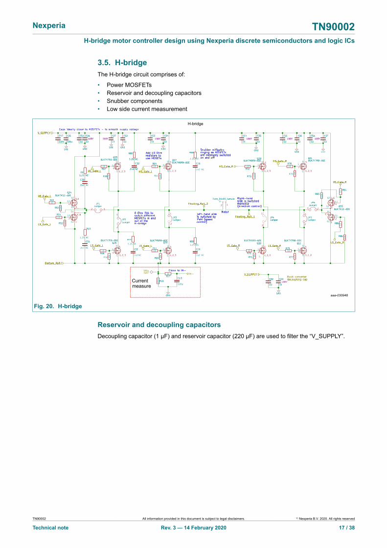
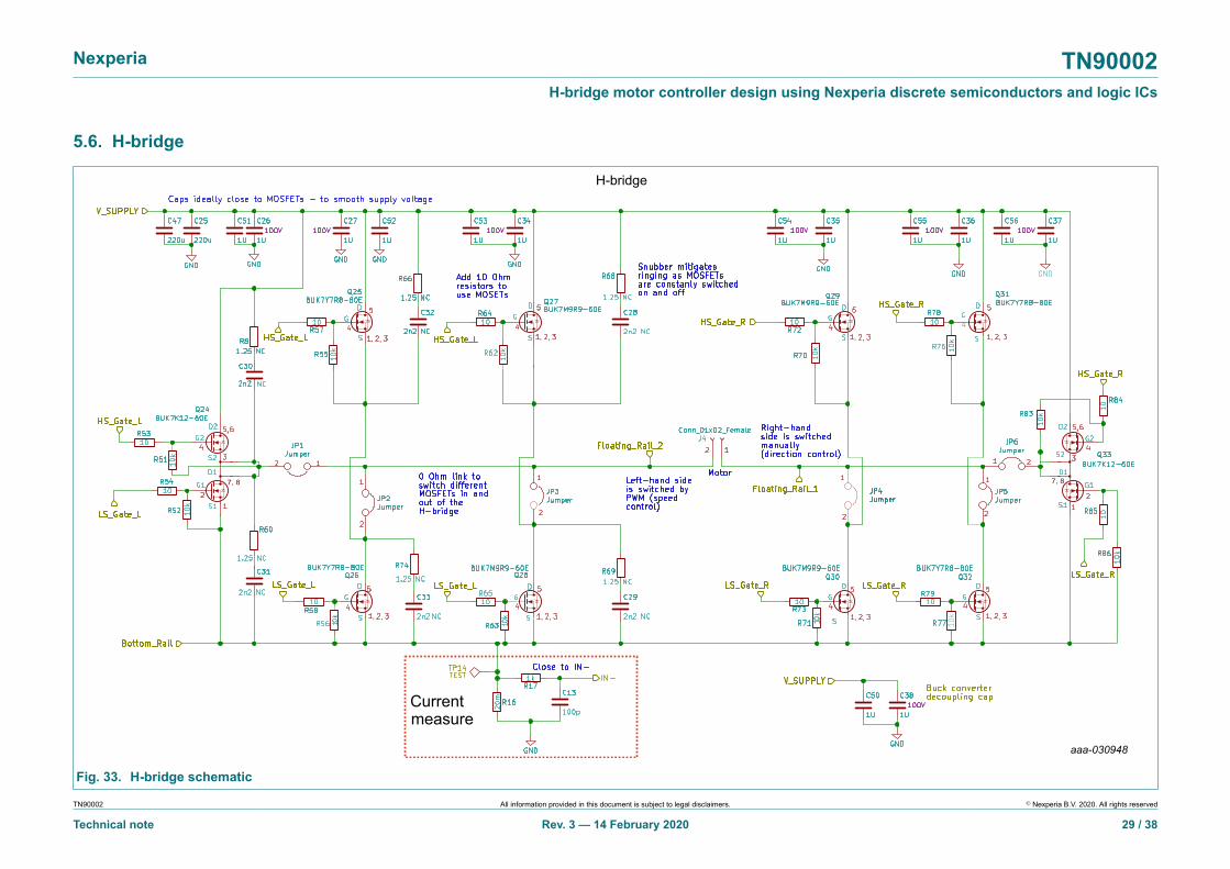
3.5. H-bridgeThe H-bridge circuit comprises of:
• Power MOSFETs• Reservoir and decoupling capacitors• Snubber components• Low side current measurement
,
7, 8
, , , ,
, , , , , , , ,
, ,, ,
,
7, 8
H-bridge
Currentmeasure
aaa-030948
Fig. 20. H-bridge
Reservoir and decoupling capacitorsDecoupling capacitor (1 μF) and reservoir capacitor (220 μF) are used to filter the “V_SUPPLY”.
TN90002 All information provided in this document is subject to legal disclaimers. © Nexperia B.V. 2020. All rights reserved
Technical note Rev. 3 — 14 February 2020 17 / 38
Nexperia TN90002H-bridge motor controller design using Nexperia discrete semiconductors and logic ICs
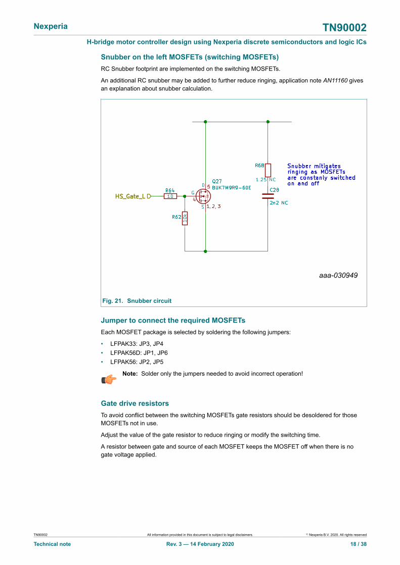
Snubber on the left MOSFETs (switching MOSFETs)RC Snubber footprint are implemented on the switching MOSFETs.
An additional RC snubber may be added to further reduce ringing, application note AN11160 givesan explanation about snubber calculation.
, ,
aaa-030949
Fig. 21. Snubber circuit
Jumper to connect the required MOSFETsEach MOSFET package is selected by soldering the following jumpers:
• LFPAK33: JP3, JP4• LFPAK56D: JP1, JP6• LFPAK56: JP2, JP5
Note: Solder only the jumpers needed to avoid incorrect operation!
Gate drive resistorsTo avoid conflict between the switching MOSFETs gate resistors should be desoldered for thoseMOSFETs not in use.
Adjust the value of the gate resistor to reduce ringing or modify the switching time.
A resistor between gate and source of each MOSFET keeps the MOSFET off when there is nogate voltage applied.
TN90002 All information provided in this document is subject to legal disclaimers. © Nexperia B.V. 2020. All rights reserved
Technical note Rev. 3 — 14 February 2020 18 / 38
Nexperia TN90002H-bridge motor controller design using Nexperia discrete semiconductors and logic ICs
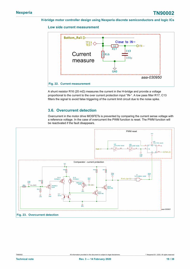
Low side current measurement
Currentmeasure
aaa-030950Fig. 22. Current measurement
A shunt resistor R16 (20 mΩ) measures the current in the H-bridge and provide a voltageproportional to the current to the over current protection input ”IN-“. A low pass filter R17, C13filters the signal to avoid false triggering of the current limit circuit due to the noise spike.
3.6. Overcurrent detectionOvercurrent in the motor drive MOSFETs is prevented by comparing the current sense voltage witha reference voltage. In the case of overcurrent the PWM function is reset. The PWM function willbe reactivated if the fault disappears.
PWM reset
Comparator - current protection
aaa-030951
Fig. 23. Overcurrent detection
TN90002 All information provided in this document is subject to legal disclaimers. © Nexperia B.V. 2020. All rights reserved
Technical note Rev. 3 — 14 February 2020 19 / 38
Nexperia TN90002H-bridge motor controller design using Nexperia discrete semiconductors and logic ICs
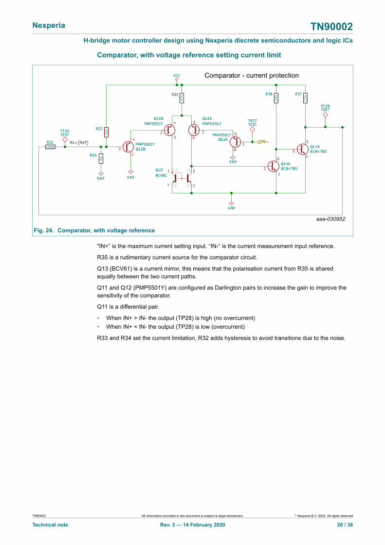
Comparator, with voltage reference setting current limit
Comparator - current protection
aaa-030952
Fig. 24. Comparator, with voltage reference
"IN+” is the maximum current setting input. “IN-“ is the current measurement input reference.
R35 is a rudimentary current source for the comparator circuit.
Q13 (BCV61) is a current mirror, this means that the polarisation current from R35 is sharedequally between the two current paths.
Q11 and Q12 (PMP5501Y) are configured as Darlington pairs to increase the gain to improve thesensitivity of the comparator.
Q11 is a differential pair.
• When IN+ > IN- the output (TP28) is high (no overcurrent)• When IN+ < IN- the output (TP28) is low (overcurrent)
R33 and R34 set the current limitation, R32 adds hysteresis to avoid transitions due to the noise.
TN90002 All information provided in this document is subject to legal disclaimers. © Nexperia B.V. 2020. All rights reserved
Technical note Rev. 3 — 14 February 2020 20 / 38
Nexperia TN90002H-bridge motor controller design using Nexperia discrete semiconductors and logic ICs
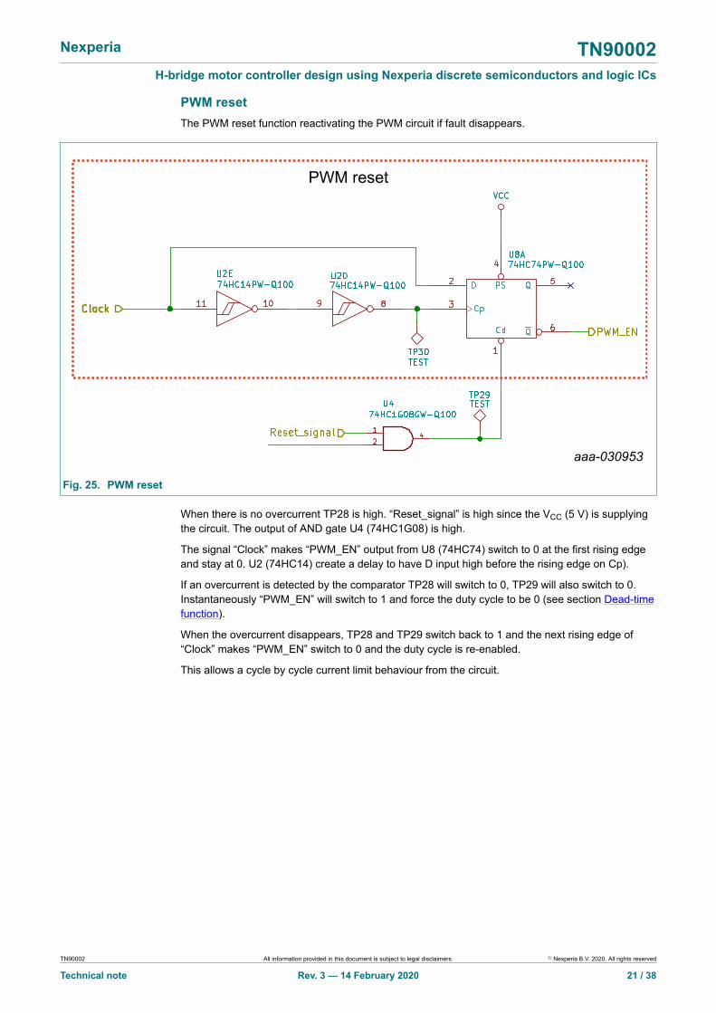
PWM resetThe PWM reset function reactivating the PWM circuit if fault disappears.
PWM reset
aaa-030953
Fig. 25. PWM reset
When there is no overcurrent TP28 is high. “Reset_signal” is high since the VCC (5 V) is supplyingthe circuit. The output of AND gate U4 (74HC1G08) is high.
The signal “Clock” makes “PWM_EN” output from U8 (74HC74) switch to 0 at the first rising edgeand stay at 0. U2 (74HC14) create a delay to have D input high before the rising edge on Cp).
If an overcurrent is detected by the comparator TP28 will switch to 0, TP29 will also switch to 0.Instantaneously “PWM_EN” will switch to 1 and force the duty cycle to be 0 (see section Dead-timefunction).
When the overcurrent disappears, TP28 and TP29 switch back to 1 and the next rising edge of“Clock” makes “PWM_EN” switch to 0 and the duty cycle is re-enabled.
This allows a cycle by cycle current limit behaviour from the circuit.
TN90002 All information provided in this document is subject to legal disclaimers. © Nexperia B.V. 2020. All rights reserved
Technical note Rev. 3 — 14 February 2020 21 / 38
Nexperia TN90002H-bridge motor controller design using Nexperia discrete semiconductors and logic ICs
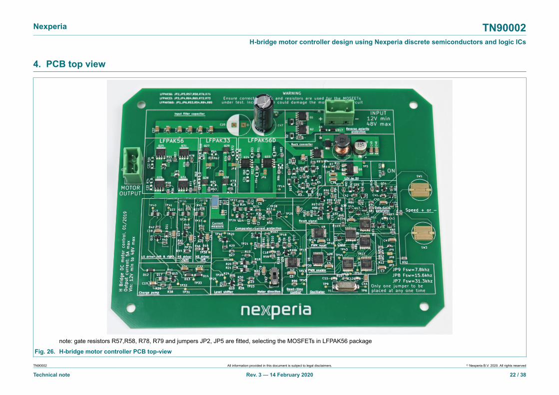
4. PCB top view
note: gate resistors R57,R58, R78, R79 and jumpers JP2, JP5 are fitted, selecting the MOSFETs in LFPAK56 package
Fig. 26. H-bridge motor controller PCB top-view
TN90002 All information provided in this document is subject to legal disclaimers. © Nexperia B.V. 2020. All rights reserved
Technical note Rev. 3 — 14 February 2020 22 / 38
Nexperia TN90002H-bridge motor controller design using Nexperia discrete semiconductors and logic ICs
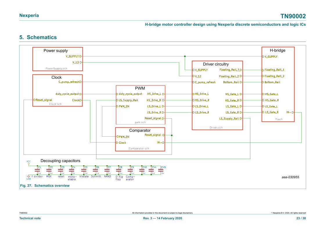
5. Schematics
Power supply
Clock
Driver circuitry
PWM
H-bridge
Comparator
Decoupling capacitors
aaa-030955
Fig. 27. Schematics overview
TN90002 All information provided in this document is subject to legal disclaimers. © Nexperia B.V. 2020. All rights reserved
Technical note Rev. 3 — 14 February 2020 23 / 38
Nexperia TN90002H-bridge motor controller design using Nexperia discrete semiconductors and logic ICs
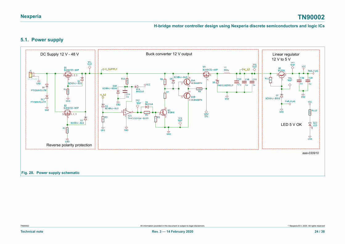
5.1. Power supply
Reverse polarity protection
Buck converter 12 V outputDC Supply 12 V - 48 V Linear regulator
, ,
, ,
LED 5 V OK
12 V to 5 V
aaa-030910
Fig. 28. Power supply schematic
TN90002 All information provided in this document is subject to legal disclaimers. © Nexperia B.V. 2020. All rights reserved
Technical note Rev. 3 — 14 February 2020 24 / 38

Nexperia TN90002H-bridge motor controller design using Nexperia discrete semiconductors and logic ICs
5.2. Clock
Frequency selection jumpers Clock
aaa-030937
Fig. 29. Clock schematic
TN90002 All information provided in this document is subject to legal disclaimers. © Nexperia B.V. 2020. All rights reserved
Technical note Rev. 3 — 14 February 2020 25 / 38
Nexperia TN90002H-bridge motor controller design using Nexperia discrete semiconductors and logic ICs
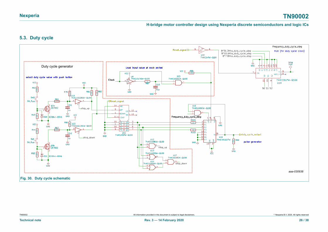
5.3. Duty cycle
Duty cycle generator
aaa-030938
Fig. 30. Duty cycle schematic
TN90002 All information provided in this document is subject to legal disclaimers. © Nexperia B.V. 2020. All rights reserved
Technical note Rev. 3 — 14 February 2020 26 / 38
Nexperia TN90002H-bridge motor controller design using Nexperia discrete semiconductors and logic ICs
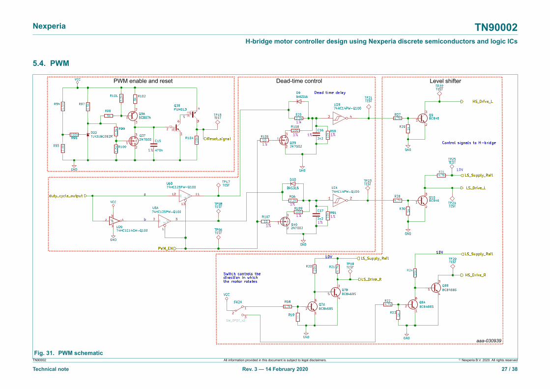
5.4. PWM
PWM enable and reset Dead-time control Level shifter
aaa-030939
Fig. 31. PWM schematicTN90002 All information provided in this document is subject to legal disclaimers. © Nexperia B.V. 2020. All rights reserved
Technical note Rev. 3 — 14 February 2020 27 / 38
Nexperia TN90002H-bridge motor controller design using Nexperia discrete semiconductors and logic ICs
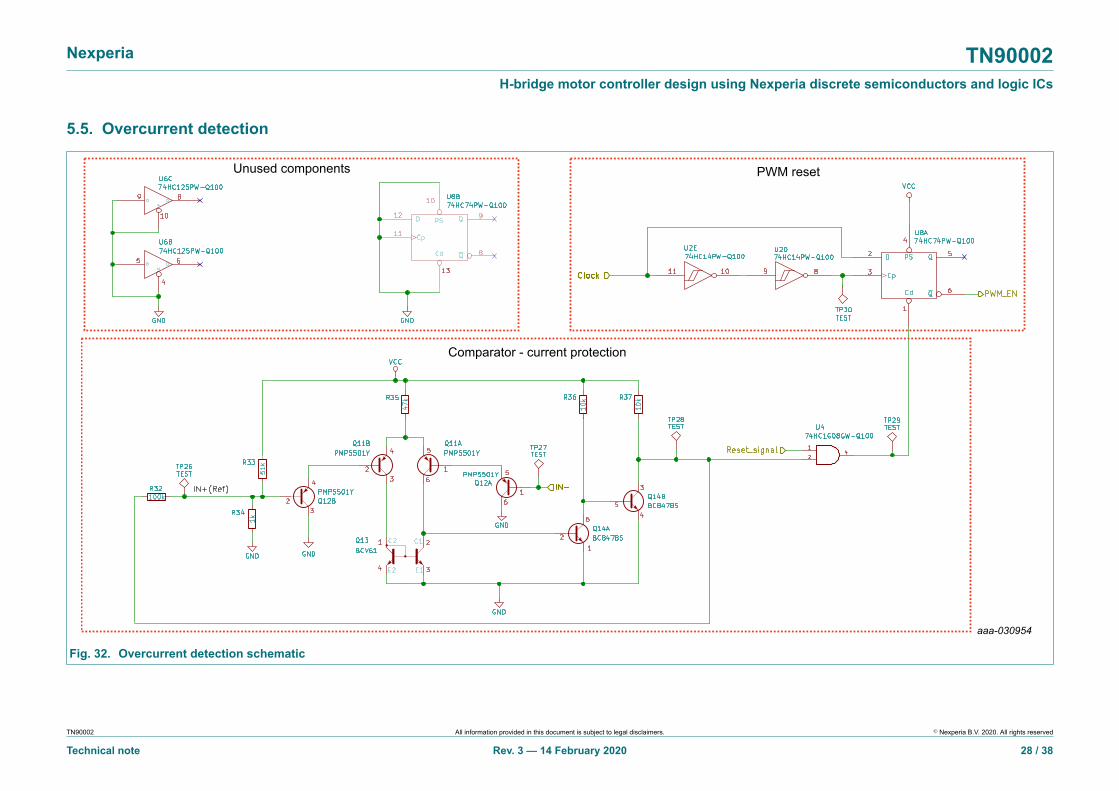
5.5. Overcurrent detection
PWM reset
Comparator - current protection
Unused components
aaa-030954
Fig. 32. Overcurrent detection schematic
TN90002 All information provided in this document is subject to legal disclaimers. © Nexperia B.V. 2020. All rights reserved
Technical note Rev. 3 — 14 February 2020 28 / 38
Nexperia TN90002H-bridge motor controller design using Nexperia discrete semiconductors and logic ICs
5.6. H-bridge
,
7, 8
, , , ,
, , , , , , , ,
, ,, ,
,
7, 8
H-bridge
Currentmeasure
aaa-030948
Fig. 33. H-bridge schematic
TN90002 All information provided in this document is subject to legal disclaimers. © Nexperia B.V. 2020. All rights reserved
Technical note Rev. 3 — 14 February 2020 29 / 38
Nexperia TN90002H-bridge motor controller design using Nexperia discrete semiconductors and logic ICs
5.7. Driver circuit
High-side driving circuit
Low-side driving circuit
aaa-030944
Fig. 34. Driver stage schematicTN90002 All information provided in this document is subject to legal disclaimers. © Nexperia B.V. 2020. All rights reserved
Technical note Rev. 3 — 14 February 2020 30 / 38
Nexperia TN90002H-bridge motor controller design using Nexperia discrete semiconductors and logic ICs
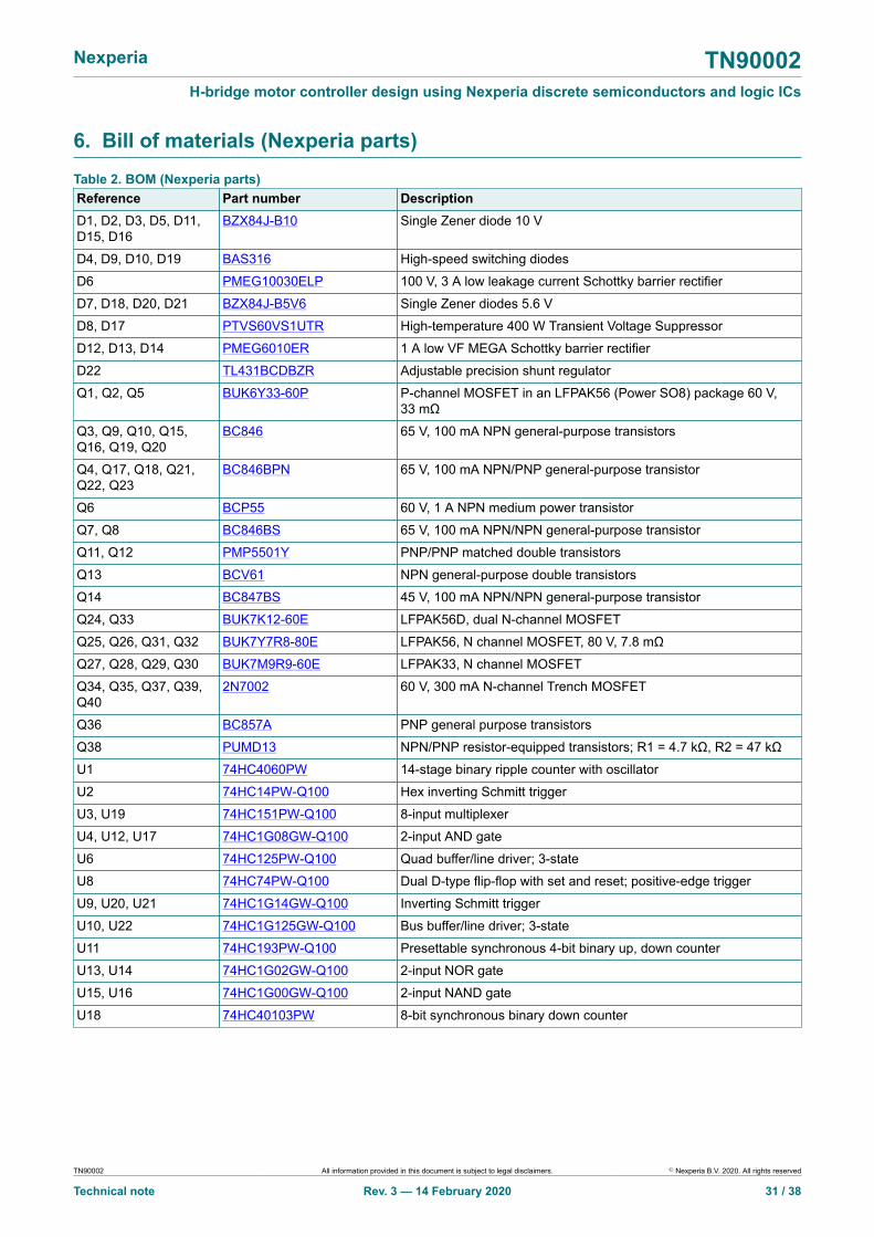
6. Bill of materials (Nexperia parts)Table 2. BOM (Nexperia parts)Reference Part number DescriptionD1, D2, D3, D5, D11,D15, D16
BZX84J-B10 Single Zener diode 10 V
D4, D9, D10, D19 BAS316 High-speed switching diodesD6 PMEG10030ELP 100 V, 3 A low leakage current Schottky barrier rectifierD7, D18, D20, D21 BZX84J-B5V6 Single Zener diodes 5.6 VD8, D17 PTVS60VS1UTR High-temperature 400 W Transient Voltage SuppressorD12, D13, D14 PMEG6010ER 1 A low VF MEGA Schottky barrier rectifierD22 TL431BCDBZR Adjustable precision shunt regulatorQ1, Q2, Q5 BUK6Y33-60P P-channel MOSFET in an LFPAK56 (Power SO8) package 60 V,
33 mΩQ3, Q9, Q10, Q15,Q16, Q19, Q20
BC846 65 V, 100 mA NPN general-purpose transistors
Q4, Q17, Q18, Q21,Q22, Q23
BC846BPN 65 V, 100 mA NPN/PNP general-purpose transistor
Q6 BCP55 60 V, 1 A NPN medium power transistorQ7, Q8 BC846BS 65 V, 100 mA NPN/NPN general-purpose transistorQ11, Q12 PMP5501Y PNP/PNP matched double transistorsQ13 BCV61 NPN general-purpose double transistorsQ14 BC847BS 45 V, 100 mA NPN/NPN general-purpose transistorQ24, Q33 BUK7K12-60E LFPAK56D, dual N-channel MOSFETQ25, Q26, Q31, Q32 BUK7Y7R8-80E LFPAK56, N channel MOSFET, 80 V, 7.8 mΩQ27, Q28, Q29, Q30 BUK7M9R9-60E LFPAK33, N channel MOSFETQ34, Q35, Q37, Q39,Q40
2N7002 60 V, 300 mA N-channel Trench MOSFET
Q36 BC857A PNP general purpose transistorsQ38 PUMD13 NPN/PNP resistor-equipped transistors; R1 = 4.7 kΩ, R2 = 47 kΩU1 74HC4060PW 14-stage binary ripple counter with oscillatorU2 74HC14PW-Q100 Hex inverting Schmitt triggerU3, U19 74HC151PW-Q100 8-input multiplexerU4, U12, U17 74HC1G08GW-Q100 2-input AND gateU6 74HC125PW-Q100 Quad buffer/line driver; 3-stateU8 74HC74PW-Q100 Dual D-type flip-flop with set and reset; positive-edge triggerU9, U20, U21 74HC1G14GW-Q100 Inverting Schmitt triggerU10, U22 74HC1G125GW-Q100 Bus buffer/line driver; 3-stateU11 74HC193PW-Q100 Presettable synchronous 4-bit binary up, down counterU13, U14 74HC1G02GW-Q100 2-input NOR gateU15, U16 74HC1G00GW-Q100 2-input NAND gateU18 74HC40103PW 8-bit synchronous binary down counter
TN90002 All information provided in this document is subject to legal disclaimers. © Nexperia B.V. 2020. All rights reserved
Technical note Rev. 3 — 14 February 2020 31 / 38
Nexperia TN90002H-bridge motor controller design using Nexperia discrete semiconductors and logic ICs
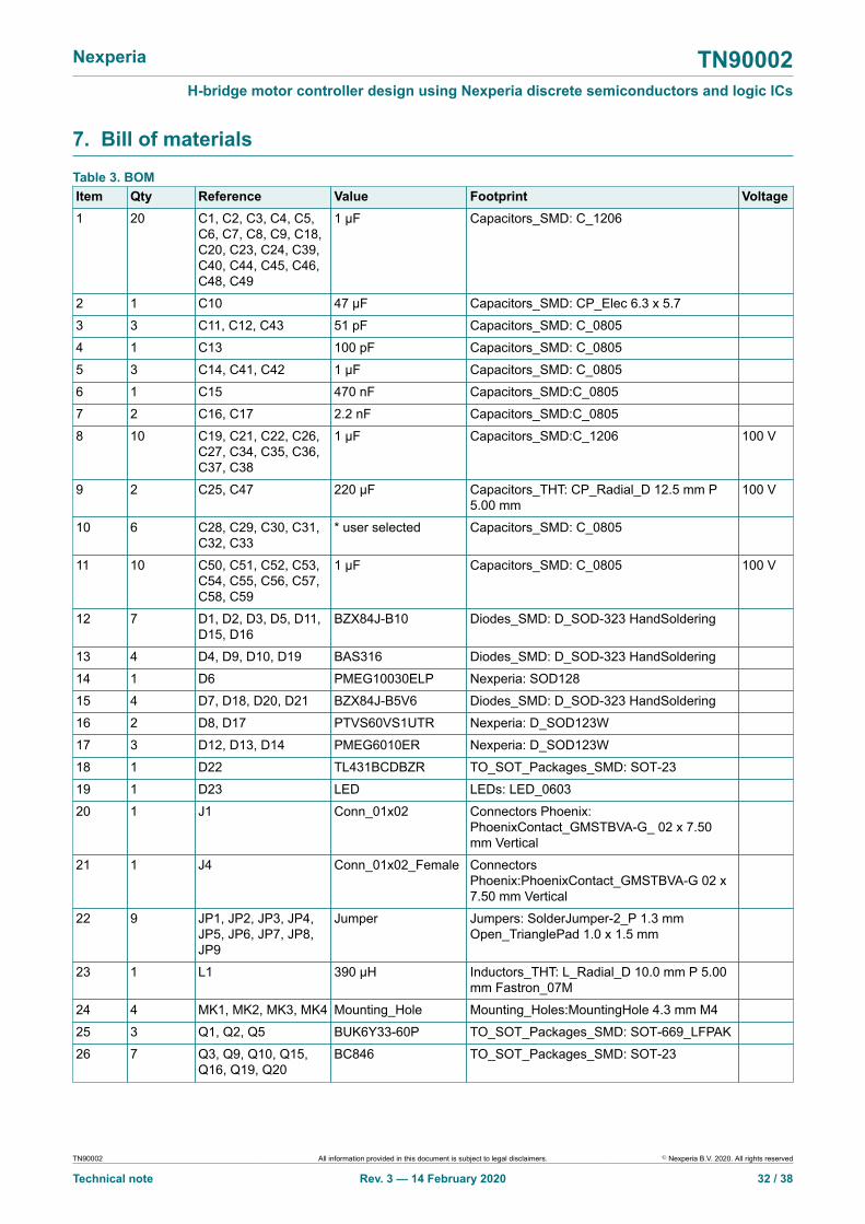
7. Bill of materialsTable 3. BOMItem Qty Reference Value Footprint Voltage1 20 C1, C2, C3, C4, C5,
C6, C7, C8, C9, C18,C20, C23, C24, C39,C40, C44, C45, C46,C48, C49
1 µF Capacitors_SMD: C_1206
2 1 C10 47 µF Capacitors_SMD: CP_Elec 6.3 x 5.73 3 C11, C12, C43 51 pF Capacitors_SMD: C_08054 1 C13 100 pF Capacitors_SMD: C_08055 3 C14, C41, C42 1 µF Capacitors_SMD: C_08056 1 C15 470 nF Capacitors_SMD:C_08057 2 C16, C17 2.2 nF Capacitors_SMD:C_08058 10 C19, C21, C22, C26,
C27, C34, C35, C36,C37, C38
1 µF Capacitors_SMD:C_1206 100 V
9 2 C25, C47 220 µF Capacitors_THT: CP_Radial_D 12.5 mm P5.00 mm
100 V
10 6 C28, C29, C30, C31,C32, C33
* user selected Capacitors_SMD: C_0805
11 10 C50, C51, C52, C53,C54, C55, C56, C57,C58, C59
1 µF Capacitors_SMD: C_0805 100 V
12 7 D1, D2, D3, D5, D11,D15, D16
BZX84J-B10 Diodes_SMD: D_SOD-323 HandSoldering
13 4 D4, D9, D10, D19 BAS316 Diodes_SMD: D_SOD-323 HandSoldering14 1 D6 PMEG10030ELP Nexperia: SOD12815 4 D7, D18, D20, D21 BZX84J-B5V6 Diodes_SMD: D_SOD-323 HandSoldering16 2 D8, D17 PTVS60VS1UTR Nexperia: D_SOD123W17 3 D12, D13, D14 PMEG6010ER Nexperia: D_SOD123W18 1 D22 TL431BCDBZR TO_SOT_Packages_SMD: SOT-2319 1 D23 LED LEDs: LED_060320 1 J1 Conn_01x02 Connectors Phoenix:
PhoenixContact_GMSTBVA-G_ 02 x 7.50mm Vertical
21 1 J4 Conn_01x02_Female ConnectorsPhoenix:PhoenixContact_GMSTBVA-G 02 x7.50 mm Vertical
22 9 JP1, JP2, JP3, JP4,JP5, JP6, JP7, JP8,JP9
Jumper Jumpers: SolderJumper-2_P 1.3 mmOpen_TrianglePad 1.0 x 1.5 mm
23 1 L1 390 µH Inductors_THT: L_Radial_D 10.0 mm P 5.00mm Fastron_07M
24 4 MK1, MK2, MK3, MK4 Mounting_Hole Mounting_Holes:MountingHole 4.3 mm M425 3 Q1, Q2, Q5 BUK6Y33-60P TO_SOT_Packages_SMD: SOT-669_LFPAK26 7 Q3, Q9, Q10, Q15,
Q16, Q19, Q20BC846 TO_SOT_Packages_SMD: SOT-23
TN90002 All information provided in this document is subject to legal disclaimers. © Nexperia B.V. 2020. All rights reserved
Technical note Rev. 3 — 14 February 2020 32 / 38
Nexperia TN90002H-bridge motor controller design using Nexperia discrete semiconductors and logic ICs
Item Qty Reference Value Footprint Voltage27 6 Q4, Q17, Q18, Q21,
Q22, Q23BC846BPN TO_SOT_Packages_SMD:
SOT-363_SC-70-6 Handsoldering28 1 Q6 BCP55 TO_SOT_Packages_SMD: SOT-223 3Lead
TabPin229 2 Q7, Q8 BC846BS TO_SOT_Packages_SMD:
SOT-363_SC-70-6 Handsoldering30 2 Q11, Q12 PMP5501Y TO_SOT_Packages_SMD:
SOT-363_SC-70-6 Handsoldering31 1 Q13 BCV61 Nexperia: SOT-143B32 1 Q14 BC847BS TO_SOT_Packages_SMD:
SOT-363_SC-70-6 Handsoldering33 2 Q24, Q33 BUK7K12-60E Nexperia: LFPAK56D34 4 Q25, Q26, Q31, Q32 BUK7Y7R8-80E TO_SOT_Packages_SMD: SOT-669_LFPAK35 4 Q27, Q28, Q29, Q30 BUK7M9R9-60E Nexperia: LFPAK3336 5 Q34, Q35, Q37, Q39,
Q402N7002 TO_SOT_Packages_SMD: SOT-23
37 1 Q36 BC857A TO_SOT_Packages_SMD: SOT-2338 1 Q38 PUMD13 TO_SOT_Packages_SMD: SOT-363
SC-70-6 Handsoldering39 2 R1, R2 10 kΩ Resistors_SMD: R_120640 14 R3, R11, R17, R19,
R23, R29, R30, R34,R39, R40, R42, R48,R50, R87
1 kΩ Resistors_SMD: R_0805
41 34 R4, R6, R12, R13,R14, R20, R24, R36,R37, R44, R45, R46,R47, R49, R51, R52,R55, R56, R59, R62,R63, R70, R71, R76,R77, R81, R82, R83,R86, R88, R89, R91,R92, R104
10 kΩ Resistors_SMD: R_0805
42 10 R5, R7, R18, R21,R22, R27, R28, R31,R38, R41
4.7 kΩ Resistors_SMD:R_0805
43 6 R8, R60, R66, R68,R69, R74
* user selected Resistors_SMD:R_0805
44 3 R9, R108, R109 100 Ω Resistors_SMD: R_080545 1 R10 20 kΩ Resistors_SMD: R_120646 4 R15, R43, R80, R93 1 MΩ Resistors_SMD: R_080547 1 R16 20 mΩ Resistors_SMD: R_251248 3 R25, R26, R101 2.2 kΩ Resistors_SMD: R_080549 4 R32, R61, R67, R96 100 kΩ Resistors_SMD: R_080550 1 R33 51 kΩ Resistors_SMD: R_080551 1 R35 47 kΩ Resistors_SMD: R_080552 17 R53, R54, R57, R58,
R64, R65, R72, R73,R78, R79, R84, R85,R90, R103, R105,R106, R107
10 Ω Resistors_SMD: R_0805
TN90002 All information provided in this document is subject to legal disclaimers. © Nexperia B.V. 2020. All rights reserved
Technical note Rev. 3 — 14 February 2020 33 / 38

Nexperia TN90002H-bridge motor controller design using Nexperia discrete semiconductors and logic ICs
Item Qty Reference Value Footprint Voltage53 1 R75 510 kΩ Resistors_SMD: R_080554 4 R94, R97, R99, R100 1.5 kΩ Resistors_SMD: R_080555 1 R95 2.4 kΩ Resistors_SMD: R_080556 2 R98, R102 5 kΩ Resistors_SMD: R_080557 1 R110 500 Ω Resistors_SMD: R_080558 2 SW1, SW3 SW_Push Buttons_Switches_SMD: SW_DIP_x1_W
8.61 mm_Slide_LowProfile59 1 SW2 SW_DPDT_x2 Buttons_Switches_THT:
SW_CuK_JS202011CQN_DPDT_Straight60 1 U1 74HC4060PW Housings_SSOP: TSSOP-16 4.4 x 5 mm
Pitch 0.65 mm61 1 U2 74HC14PW-Q100 Housings_SSOP: TSSOP-14 4.4 x 5
mm_Pitch 0.65mm62 2 U3, U19 74HC151PW-Q100 Housings_SSOP: TSSOP-16 4.4 x 5 mm
Pitch 0.65 mm63 3 U4, U12, U17 74HC1G08GW-Q100 TO_SOT_Packages_SMD:
SOT-353_SC-70-564 1 U6 74HC125PW-Q100 Housings_SSOP: TSSOP-14 4.4 x 5mm
Pitch 0.65 mm65 1 U8 74HC74PW-Q100 Housings_SSOP: TSSOP-14 4.4 x 5 mm
Pitch 0.65 mm66 3 U9, U20, U21 74HC1G14GW-Q100 TO_SOT_Packages_SMD:
SOT-353_SC-70-567 2 U10, U22 74HC1G125GW-
Q100TO_SOT_Packages_SMD:SOT-353_SC-70-5
68 1 U11 74HC193PW-Q100 Housings_SSOP: TSSOP-16 4.4 x 5mmPitch 0.65 mm
69 2 U13, U14 74HC1G02GW-Q100 TO_SOT_Packages_SMD:SOT-353_SC-70-5
70 2 U15, U16 74HC1G00GW-Q100 TO_SOT_Packages_SMD:SOT-353_SC-70-5
71 1 U18 74HC40103PW Housings_SSOP: TSSOP-16 4.4 x 5 mmPitch 0.65 mm
72 1 Y1 Crystal Crystals: Crystal_SMD_HC49-SD
8. Revision historyTable 4. Revision historyRevisionnumber
Date Description
3.0 20200214 Schematic diagrams, text and BOMs updated to latest type numbers for Q1,Q2 and Q52.0 20190422 Schematic diagrams updated to correct IC type numbers1.0 20190215 Initial version of the document
TN90002 All information provided in this document is subject to legal disclaimers. © Nexperia B.V. 2020. All rights reserved
Technical note Rev. 3 — 14 February 2020 34 / 38
Nexperia TN90002H-bridge motor controller design using Nexperia discrete semiconductors and logic ICs
9. Legal information
DefinitionsDraft — The document is a draft version only. The content is still underinternal review and subject to formal approval, which may result inmodifications or additions. Nexperia does not give any representations orwarranties as to the accuracy or completeness of information included hereinand shall have no liability for the consequences of use of such information.
DisclaimersLimited warranty and liability — Information in this document is believedto be accurate and reliable. However, Nexperia does not give anyrepresentations or warranties, expressed or implied, as to the accuracyor completeness of such information and shall have no liability for theconsequences of use of such information. Nexperia takes no responsibilityfor the content in this document if provided by an information source outsideof Nexperia.
In no event shall Nexperia be liable for any indirect, incidental, punitive,special or consequential damages (including - without limitation - lostprofits, lost savings, business interruption, costs related to the removalor replacement of any products or rework charges) whether or not suchdamages are based on tort (including negligence), warranty, breach ofcontract or any other legal theory.
Notwithstanding any damages that customer might incur for any reasonwhatsoever, Nexperia’s aggregate and cumulative liability towards customerfor the products described herein shall be limited in accordance with theTerms and conditions of commercial sale of Nexperia.
Right to make changes — Nexperia reserves the right to make changesto information published in this document, including without limitationspecifications and product descriptions, at any time and without notice. Thisdocument supersedes and replaces all information supplied prior to thepublication hereof.
Suitability for use — Nexperia products are not designed, authorized orwarranted to be suitable for use in life support, life-critical or safety-criticalsystems or equipment, nor in applications where failure or malfunctionof an Nexperia product can reasonably be expected to result in personalinjury, death or severe property or environmental damage. Nexperia and itssuppliers accept no liability for inclusion and/or use of Nexperia products insuch equipment or applications and therefore such inclusion and/or use is atthe customer’s own risk.
Applications — Applications that are described herein for any of theseproducts are for illustrative purposes only. Nexperia makes no representationor warranty that such applications will be suitable for the specified usewithout further testing or modification.
Customers are responsible for the design and operation of their applicationsand products using Nexperia products, and Nexperia accepts no liability forany assistance with applications or customer product design. It is customer’ssole responsibility to determine whether the Nexperia product is suitableand fit for the customer’s applications and products planned, as well asfor the planned application and use of customer’s third party customer(s).Customers should provide appropriate design and operating safeguards tominimize the risks associated with their applications and products.
Nexperia does not accept any liability related to any default, damage, costsor problem which is based on any weakness or default in the customer’sapplications or products, or the application or use by customer’s third partycustomer(s). Customer is responsible for doing all necessary testing for thecustomer’s applications and products using Nexperia products in order toavoid a default of the applications and the products or of the application oruse by customer’s third party customer(s). Nexperia does not accept anyliability in this respect.
Export control — This document as well as the item(s) described hereinmay be subject to export control regulations. Export might require a priorauthorization from competent authorities.
Translations — A non-English (translated) version of a document is forreference only. The English version shall prevail in case of any discrepancybetween the translated and English versions.
TrademarksNotice: All referenced brands, product names, service names andtrademarks are the property of their respective owners.
TN90002 All information provided in this document is subject to legal disclaimers. © Nexperia B.V. 2020. All rights reserved
Technical note Rev. 3 — 14 February 2020 35 / 38

Nexperia TN90002H-bridge motor controller design using Nexperia discrete semiconductors and logic ICs
List of TablesTable 1. Duty cycle selection............................................... 9Table 2. BOM (Nexperia parts).......................................... 31Table 3. BOM..................................................................... 32Table 4. Revision history....................................................34
TN90002 All information provided in this document is subject to legal disclaimers. © Nexperia B.V. 2020. All rights reserved
Technical note Rev. 3 — 14 February 2020 36 / 38
Nexperia TN90002H-bridge motor controller design using Nexperia discrete semiconductors and logic ICs
List of FiguresFig. 1. Simplified MOSFET H-bridge motor control..............2Fig. 2. H-bridge motor controller block diagram...................3Fig. 3. Power supply circuit..................................................4Fig. 4. Transient overvoltage protection...............................4Fig. 5. Reverse polarity protection....................................... 5Fig. 6. Buck converter.......................................................... 6Fig. 7. Linear regulator.........................................................6Fig. 8. Clock, duty cycle and frequency selection................ 7Fig. 9. Oscillator and frequency divider............................... 8Fig. 10. Duty cycle............................................................... 9Fig. 11. PWM, dead-time, level shifting and directionselection............................................................................. 10Fig. 12. Reset circuit.......................................................... 11Fig. 13. Dead-time function and PWM enable................... 12Fig. 14. Level shifter...........................................................13Fig. 15. Direction selection.................................................13Fig. 16. Driver circuit.......................................................... 14Fig. 17. High side driver circuit.......................................... 15Fig. 18. Low side driver circuit........................................... 15Fig. 19. Charge pump........................................................ 16Fig. 20. H-bridge................................................................ 17Fig. 21. Snubber circuit...................................................... 18Fig. 22. Current measurement........................................... 19Fig. 23. Overcurrent detection........................................... 19Fig. 24. Comparator, with voltage reference...................... 20Fig. 25. PWM reset............................................................ 21Fig. 26. H-bridge motor controller PCB top-view................22Fig. 27. Schematics overview............................................ 23Fig. 28. Power supply schematic....................................... 24Fig. 29. Clock schematic....................................................25Fig. 30. Duty cycle schematic............................................ 26Fig. 31. PWM schematic.................................................... 27Fig. 32. Overcurrent detection schematic.......................... 28Fig. 33. H-bridge schematic............................................... 29Fig. 34. Driver stage schematic......................................... 30
TN90002 All information provided in this document is subject to legal disclaimers. © Nexperia B.V. 2020. All rights reserved
Technical note Rev. 3 — 14 February 2020 37 / 38
Nexperia TN90002H-bridge motor controller design using Nexperia discrete semiconductors and logic ICs
Contents1. Introduction...................................................................22. Block diagram and system functionality.................... 32.1. Subsystems overview............................................... 33. Subsystem descriptions.............................................. 43.1. Power supply............................................................... 43.2. Clock and duty cycle generator................................... 73.3. Pulse Width Modulation.............................................103.4. Drive circuit................................................................143.5. H-bridge..................................................................... 173.6. Overcurrent detection................................................ 194. PCB top view.............................................................. 225. Schematics..................................................................235.1. Power supply............................................................. 245.2. Clock..........................................................................255.3. Duty cycle..................................................................265.4. PWM.......................................................................... 275.5. Overcurrent detection................................................ 285.6. H-bridge..................................................................... 295.7. Driver circuit...............................................................306. Bill of materials (Nexperia parts).............................. 317. Bill of materials...........................................................328. Revision history..........................................................349. Legal information........................................................35
© Nexperia B.V. 2020. All rights reservedFor more information, please visit: http://www.nexperia.comFor sales office addresses, please send an email to: [email protected] of release: 14 February 2020
TN90002 All information provided in this document is subject to legal disclaimers. © Nexperia B.V. 2020. All rights reserved
Technical note Rev. 3 — 14 February 2020 38 / 38
Related Documents


![Discrete-Time Fractional-Order PID Controller: Definition ... · arXiv:1405.0144v1 [math.OC] 1 May 2014 Discrete-Time Fractional-Order PID Controller: Definition, Tuning, Digital](https://static.cupdf.com/doc/110x72/6040056c21c2e7483c0cd8e3/discrete-time-fractional-order-pid-controller-deinition-arxiv14050144v1.jpg)