1 of 109 Semtech Proprietary & Confidential GS12070 Final Data Sheet Rev.6 PDS-061012 February 2018 GS12070 UHD-SDI Gearbox www.semtech.com Key Features • Fully standards compliant turnkey solution enabling a simplified UHD-SDI interface • Converts between HD-SDI, 3G-SDI, 6G UHD-SDI, and 12G UHD-SDI using MUX (Multiplex) and DeMUX (Demultiplex) modes • Quad Link 3G-SDI Single Link 12G UHD-SDI • Quad Link (1.5Gb/s x 4) HD-SDI Single Link 6Gb/s • Quad Link 6G UHD-SDI Dual Link 12G UHD-SDI • Quad Link 3G-SDI (ST 425-5/6) Dual Link 6G UHD-SDI • Dual Link 6G UHD-SDI Single Link 12G UHD-SDI • Dual Link 3G-SDI (ST 425-3) Single Link 6G UHD-SDI • Dual Link (1.5Gb/s x 2) HD-SDI Single Link 3Gb/s • Bypass modes for all supported rates, including SD • Automatic skew compensation for multi-link inputs • Automatic input link order handling for multi-link 3Gb/s input • Configurable Serial Output assignment • Configurable multi-link output delay • 100Ω Differential Inputs • Input trace equalization up to 12dB • Four 100Ω Differential Outputs • Individually selectable output swing • Reference Clock/Crystal Input — 27MHz • GSPI Serial Control and Monitoring Interface • Automatic and manual SMPTE ST 352M handling • 12mm x 12mm 196-Ball BGA (0.8mm pitch) • Pb-free/Halogen-free/RoHS/WEEE compliant package Applications • Next Generation 3D/2D HFR HDTV and 2K D-Cinema, UHDTV1 and 4K D-Cinema end-equipment: Cameras, Monitors, Switchers, etc. • Next Generation 3G-SDI, 6G UHD-SDI, and 12G UHD-SDI infrastructures designed in support of UHDTV1, UHDTV2, 4K D-Cinema and 3D HFR, HDR production image formats, and 6G UHD-SDI/12G UHD-SDI multiplexing and de-multiplexing for integration into legacy infrastructure. Description The GS12070 is a highly configurable UHD-SDI Gearbox which performs multiplexing and de-multiplexing necessary to facilitate conversions between SMPTE ST 425-3 and/or ST 425-5 (multi-link 3G-SDI) Interface and SMPTE ST 2081-1 (6G UHD-SDI) and/or ST 2082-1 (12G UHD-SDI) Interfaces. The Gearbox also supports conversion between 4 x HD-SDI and 6Gb/s SDI. Example of Multiplexing ST 425-5 into ST 2081-1 (6Gb/s) and ST 2082-1 (12Gb/s) For the supported SMPTE conversions, the SMPTE ST 352 payload identification will be automatically detected and replaced based on the user selected conversion mode. This can be bypassed for proprietary multiplexing and demultiplexing links. The device incorporates the ability to reorder the output serial stream and duplicate outputs to unused output channels or route any input channel. The GS12070 has the ability to automatically compensate for up to 400ns of skew between QL 6Gb/s or DL 12Gb/s inputs and 800ns of skew between DL 6Gb/s and QL 3Gb/s inputs. This aids in any lane-to-lane variance introduced by cable mismatch or upstream routing and distribution equipment. 3840 x 2160 p60 4:2:2 10-bit ST 425-5 Quad-link 3G ST 2081-11 Dual-link 6G ST 2082-10 Single-link 12G 4 x 3G ↔ 12G 4 x 3G ↔ 2 x 6G 2 x 6G ↔ 12G

Welcome message from author
This document is posted to help you gain knowledge. Please leave a comment to let me know what you think about it! Share it to your friends and learn new things together.
Transcript

1 of 109Semtech
Proprietary & Confidential
GS12070Final Data Sheet Rev.6PDS-061012 February 2018
GS12070
UHD-SDI Gearbox
www.semtech.com
Key Features• Fully standards compliant turnkey solution enabling a
simplified UHD-SDI interface• Converts between HD-SDI, 3G-SDI, 6G UHD-SDI, and
12G UHD-SDI using MUX (Multiplex) and DeMUX (Demultiplex) modes
• Quad Link 3G-SDI Single Link 12G UHD-SDI• Quad Link (1.5Gb/s x 4) HD-SDI Single Link 6Gb/s• Quad Link 6G UHD-SDI Dual Link 12G UHD-SDI• Quad Link 3G-SDI (ST 425-5/6) Dual Link 6G
UHD-SDI• Dual Link 6G UHD-SDI Single Link 12G UHD-SDI• Dual Link 3G-SDI (ST 425-3) Single Link 6G
UHD-SDI• Dual Link (1.5Gb/s x 2) HD-SDI Single Link 3Gb/s
• Bypass modes for all supported rates, including SD• Automatic skew compensation for multi-link inputs• Automatic input link order handling for multi-link
3Gb/s input • Configurable Serial Output assignment• Configurable multi-link output delay• 100Ω Differential Inputs
• Input trace equalization up to 12dB• Four 100Ω Differential Outputs
• Individually selectable output swing• Reference Clock/Crystal Input — 27MHz• GSPI Serial Control and Monitoring Interface• Automatic and manual SMPTE ST 352M handling• 12mm x 12mm 196-Ball BGA (0.8mm pitch)• Pb-free/Halogen-free/RoHS/WEEE compliant package
Applications• Next Generation 3D/2D HFR HDTV and 2K D-Cinema,
UHDTV1 and 4K D-Cinema end-equipment: Cameras, Monitors, Switchers, etc.
• Next Generation 3G-SDI, 6G UHD-SDI, and 12G UHD-SDI infrastructures designed in support of UHDTV1, UHDTV2, 4K D-Cinema and 3D HFR, HDR production image formats, and 6G UHD-SDI/12G UHD-SDI multiplexing and de-multiplexing for integration into legacy infrastructure.
DescriptionThe GS12070 is a highly configurable UHD-SDI Gearbox which performs multiplexing and de-multiplexing necessary to facilitate conversions between SMPTE ST 425-3 and/or ST 425-5 (multi-link 3G-SDI) Interface and SMPTE ST 2081-1 (6G UHD-SDI) and/or ST 2082-1 (12G UHD-SDI) Interfaces. The Gearbox also supports conversion between 4 x HD-SDI and 6Gb/s SDI.
Example of Multiplexing ST 425-5 into ST 2081-1 (6Gb/s) and ST 2082-1 (12Gb/s)
For the supported SMPTE conversions, the SMPTE ST 352 payload identification will be automatically detected and replaced based on the user selected conversion mode. This can be bypassed for proprietary multiplexing and demultiplexing links.
The device incorporates the ability to reorder the output serial stream and duplicate outputs to unused output channels or route any input channel.
The GS12070 has the ability to automatically compensate for up to 400ns of skew between QL 6Gb/s or DL 12Gb/s inputs and 800ns of skew between DL 6Gb/s and QL 3Gb/s inputs. This aids in any lane-to-lane variance introduced by cable mismatch or upstream routing and distribution equipment.
3840 x 2160 p60 4:2:2 10-bit
ST 425-5Quad-link 3G
ST 2081-11Dual-link 6G
ST 2082-10Single-link 12G
4 x 3G ↔ 12G
4 x 3G ↔ 2 x 6G 2 x 6G ↔ 12G

GS12070 Block Diagram
Control,GSPI
XTAL_IN
XTAL_OUT
TxDDO0
TxDDO1
TxDDO2
CS
TxDDO3
DDI3Rx
DDI2Rx
DDI1Rx
DDI0Rx
MUX/DEMUX
ST 352 &CRC
insertion
ChannelReassignment
DDI0
DDI1
DDI2
DDI3
DDO0
DDO1
DDO2
DDO3
Input Video Detection and Status
Input Video Detection and Status
Input Video Detection and Status
Input Video Detection and Status
ISP[3:0]
REFCLK_SEL[1:0]
RESET
BYPA
SS
JTAGController
SD_B
YPAS
S[3:
0]
SCLK
SDIN
SDO
UT
TMS
TRST
TDO
TCK
MU
X/D
EMU
X
MO
DE_
SEL[
2:0]
PID
_MO
DE[
1:0]
REXT
_TX
REXT
_RX
TIM_OUT[3:0]
STAT[15:0]
RX_CLK_[3:0]
VCC_IO VCC_A_1V8 VCC_A_1V1 VCC_CORE VSS
TX_P
CLK[
1:0]
LIN
K_AS
GM
T SE
C_LI
NK_
ENAB
LE
DEM
UX_
INPU
T_SE
LECT
SYS_RESET
TD1
GS12070Final Data Sheet Rev.6PDS-061012 February 2018
2 of 109Semtech
Proprietary & Confidential
www.semtech.com

Revision History
Contents
1. Pin Out .................................................................................................................................................................6
1.1 Pin Assignment ...................................................................................................................................6
1.2 Pin Descriptions ..................................................................................................................................7
2. Electrical Characteristics............................................................................................................................. 11
2.1 Absolute Maximum Ratings ........................................................................................................ 11
2.2 DC Electrical Characteristics ........................................................................................................ 11
2.3 AC Electrical Characteristics ......................................................................................................... 14
2.4 Latency ................................................................................................................................................ 15
3. Detailed Description.................................................................................................................................... 16
3.1 Power Supply Considerations ..................................................................................................... 16
3.1.1 Power Connections ............................................................................................................ 16
3.1.2 Power On Sequence........................................................................................................... 16
3.1.3 Device Initialization ............................................................................................................ 17
3.2 Power On Reset ................................................................................................................................ 17
3.3 Serial Data Inputs ............................................................................................................................. 18
3.3.1 Input Signal Interface Levels ........................................................................................... 18
3.3.2 Input Trace Equalization ................................................................................................... 18
Version ECO Date Changes and/or Modifications
6 040676 February 2018Added Section 3.12.3, PRBS Data Bypass.Added Section 3.5.1, DDI CDR Reference Clock Configuration.
5 035260 January 2017
Added Section 2.4, Latency.Added Section 3.9.3, Input Tx Clock Selection.Added Section 3.14, Embedded Video Pattern Generator.Added Host Interface Register Map, Section 4.Added Figure 3-12 GL12G-SL6G Output Link Assignment.Added Figure 6-4 GS12070 Marking DiagramUpdated Section 2.2, Section 2.3, Table 6-1
4 034133 November 2016
Added Section 3.3.4 on output power down.Added Section 3.2 on device reset.Updated Figure , Table 2-1, Table 2-2, Table 2-3, Table 3-35
3 034034 October 2016 Updates to add information to Section 3.
2 028141 October 2015Updated pin names in Figure 1-1, Table 1-1, Table 3-7, and Table 3-8.
1 026325 June 2015 Minor correction on Page 1.
0 025710 June 2015 New document.
GS12070Final Data Sheet Rev.6PDS-061012 February 2018
3 of 109Semtech
Proprietary & Confidential
www.semtech.com

3.3.3 Input Signal Present ........................................................................................................... 19
3.3.4 Input Power-Down ............................................................................................................. 19
3.4 Serial Data Outputs ......................................................................................................................... 19
3.4.1 DDO Output Swing............................................................................................................. 19
3.4.2 Output Idle............................................................................................................................. 20
3.4.3 Output Power-Down.......................................................................................................... 20
3.4.4 Output Driver Disable........................................................................................................ 22
3.5 Reference Clock ................................................................................................................................ 22
3.5.1 DDI CDR Reference Clock Configuration .................................................................... 22
3.6 Digital I/O ........................................................................................................................................... 23
3.7 Modes of Operation ........................................................................................................................ 23
3.7.1 Operating Mode Selection............................................................................................... 23
3.8 Input Serial Receiver and Input Processing Operation ...................................................... 24
3.8.1 Input Data Rate .................................................................................................................... 24
3.8.2 Input Loop Bandwidth ...................................................................................................... 25
3.8.3 Automatic Skew Tolerance .............................................................................................. 26
3.8.4 Status Reporting .................................................................................................................. 26
3.9 Serial Transmitter Operation ....................................................................................................... 28
3.9.1 Output Assignment ............................................................................................................ 28
3.9.2 Output Loop Bandwidth................................................................................................... 29
3.9.3 Transmitter Input Clock Selection................................................................................. 30
3.10 Multiplex Mode .............................................................................................................................. 30
3.10.1 Conversion Selection....................................................................................................... 30
3.10.2 Multiplexing Paths............................................................................................................ 32
3.10.3 SMPTE Compatibility ....................................................................................................... 33
3.10.4 Lost Input............................................................................................................................. 33
3.10.5 Automatic Input Link Ordering.................................................................................... 34
3.10.6 MUX Manual Input Channel Assignment................................................................. 34
3.11 Demultiplex Mode ........................................................................................................................ 35
3.11.1 Conversion Selection....................................................................................................... 35
3.11.2 Demultiplexing Paths...................................................................................................... 37
3.11.3 SMPTE Compatibility ....................................................................................................... 39
3.11.4 Lane Delay ........................................................................................................................... 39
3.11.5 DeMUX Output Link Assignment................................................................................ 40
3.12 Bypass Mode ................................................................................................................................... 42
3.12.1 Input Stream Data Rate Detection.............................................................................. 42
3.12.2 SD Bypass Mode ................................................................................................................ 42
3.12.3 PRBS Data Bypass.............................................................................................................. 42
3.13 Payload ID Handling .................................................................................................................... 43
3.13.1 Detection of Payload ID.................................................................................................. 43
3.13.2 Automatic Insertion of Payload ID.............................................................................. 46
3.13.3 Manual Insertion of Payload ID.................................................................................... 49
3.14 Embedded Video Pattern Generator ..................................................................................... 52
3.15 GSPI Host Interface ....................................................................................................................... 54
3.15.1 CS Pin..................................................................................................................................... 54
3.15.2 SDIN Pin................................................................................................................................ 55
3.15.3 SDOUT Pin ........................................................................................................................... 55
GS12070Final Data Sheet Rev.6PDS-061012 February 2018
4 of 109Semtech
Proprietary & Confidential
www.semtech.com

3.15.4 SCLK Pin................................................................................................................................ 56
3.15.5 Command Word 1 Description .................................................................................... 57
3.15.6 GSPI Transaction Timing ................................................................................................ 59
3.15.7 Single Read/Write Access............................................................................................... 61
3.15.8 Auto-increment Read/Write Access ........................................................................... 62
3.15.9 Setting a Device Unit Address...................................................................................... 62
3.15.10 Default GSPI Operation ................................................................................................ 63
4. Host Interface Register Map...................................................................................................................... 64
4.1 Control Registers ............................................................................................................................. 64
4.2 Register Descriptions ..................................................................................................................... 67
4.2.1 GS12070 Control and Status Register .......................................................................... 67
4.2.2 Rx Control and Status Register ....................................................................................... 93
4.2.3 Tx Control and Status Registers ..................................................................................... 95
4.2.4 Video Pattern Generator Control Registers ............................................................... 99
5. Application Information...........................................................................................................................103
5.1 Typical Application Circuit .........................................................................................................103
6. Package & Ordering Information ..........................................................................................................105
6.1 Package Dimensions ....................................................................................................................105
6.2 Recommended PCB Footprint ..................................................................................................106
6.3 Packaging Data ..............................................................................................................................106
6.4 Solder Reflow Profile ....................................................................................................................107
6.5 Marking Diagram ...........................................................................................................................107
6.6 Ordering Information ...................................................................................................................108
GS12070Final Data Sheet Rev.6PDS-061012 February 2018
5 of 109Semtech
Proprietary & Confidential
www.semtech.com

1. Pin Out
1.1 Pin Assignment
Figure 1-1: Pin Out
VSS DDO1 DDO0 STAT0 STAT1 STAT2 STAT3
STAT4 STAT5 RX_CLK_0
VCC_IO RSVD RSVD RSVD STAT6 STAT7 RX_CLK_1
DDO3 VCC_IO RSVD RSVD VCC_IO STAT8 STAT9 RX_CLK_2
VCC_A_1V8
VSS
VSS VSS VSS VSS
VSS
VSS
VSS
VSS
VSS
VSS
VSS
VSS
VSS
VSS
VSSVSSVSSVSS
VSS
VSSVSSVSS
VSS
VSS
VSSVSS
VSS
VSS
VSS
VSS
VSS
VSS
RSVD RSVD
NC
RSVDRSVD
RSVD
RSVD
RSVD
RSVD
RSVD
RSVD
RSVD
RSVD
RSVD
RSVD
RSVD
RSVD
RSVD
RSVD
NCNC
NCNC
VSS
VSS
DDI3
DDI2
DDI1 DDI0
VCC_IO
REXT_RX
TDI
TMS
TDO
TRST
VCC_A_1V8 VCC_A_1V1
VCC_A_1V8
VCC_A_1V8
VCC_A_1V1
VCC_A_1V1 VSS
VSS
REXT_TX
NC
VCC_CORE
VCC_CORE
VCC_CORE
VCC_CORE
VCC_CORE
VCC_CORE
VCC_IO
TCK REFCLK_SEL0
ISP0 ISP1 ISP2
SDIN
ISP3
SDOUT
RSVD
RSVD
VSS
SCLK
TIM_OUT3
TIM_OUT2
STAT14 STAT15 TIM_OUT1
STAT12 STAT13 TIM_OUT0
STAT10 STAT11 RX_CLK_3
LINK_ASGMTRSVD
RSVD
VCC_CORE
VCC_IO
VCC_IO
VCC_IO
RSVD RSVD
RSVD
REFCLK_SEL1
TX_PCLK0 TX_PCLK1
RSVD
REF_IN
PID_MODE1
PID_MODE0
SD_BYPASS0
SD_BYPASS1
SD_BYPASS2
SD_BYPASS3
MODE_SEL1
MODE_SEL2
BYPASSMODE_
SEL0
XTAL_IN
XTAL_OUT
A
B
C
D
E
F
G
H
J
K
L
M
NRSVD
RSVD
DDO1 DDO0MUX/
DEMUX
DDO3
DDI3
DDI2
DDI1
Legend:
CS
P
VSS
VSS
VSSVSS
VSS VSS
VSS VSS
VSS
VSSVSSVSS
VSS
DDI0
RESET
1 2 3 4 5 6 7 8 9 10 11 12 13 14
VSS
RESET
Clock and Timing — Output
High-speed differential inputs
High-speed differential outputs
Reference clock
Digital control and status — Input
VCC
1.8V supply
1.1V supply
I/O supply
GND
RSVD
RSVD
REF_OUT
Low-speed digital control and status (static) — Output
SYS_RESET
SEC_LINK_ENABLE
DEMUX_INPUT_SELECT
DDO2
DDO2
VCC_A_1V1
GS12070Final Data Sheet Rev.6PDS-061012 February 2018
6 of 109Semtech
Proprietary & Confidential
www.semtech.com

1.2 Pin Descriptions
Table 1-1: Pin Descriptions
Pin Number Name Type Description
A1, A6, A14, B2, B3, B4, B5, C2, C9, C10, D2, D9, E2, E7, E8, F1, F2, F8, F9, F10, G2, G5, G7, G9, H2, H5, H7, H9, J1, J2, J8, J9, J10, K2, K7, K8, L2, L7, L8, L9, M2, M9, M10, N2,
N3, N4, N5, N7, N8, N9, P1, P9, P14
VSS Power Device ground. Connect to GND.
A7 MUX/DEMUX Digital Input
Selects between Multiplex and Demultiplex mode.
This pin has an internal pull-down resistor.
This function can be overridden by the CSR.
A8 BYPASS Digital Input
When HIGH, BYPASS is active and all inputs pass data directly to the outputs.
When LOW, multiplexing/demultiplexing occurs as programmed by the MODE_SEL and PID_MODE pins.
This pin has an internal pull-down resistor.
This function can be overridden by the CSR.
B9, B8, B7, B6 SD_BYPASS[3:0] Digital Input
Selects the SD data rate per channel when in Bypass mode.
When HIGH, SD_BYPASS is active.
SD_BYPASS is only available when BYPASS is set to 1.
These pins have an internal pull-down resistor.
This function can be overridden by the CSR.
B11, B10, A9 MODE_SEL[2:0] Digital Input
Multiplex or Demultiplex conversion mode selection. See Table 3-16: MUX Mode Up Conversion and Table 3-19: DeMUX Mode Down Conversion.
These pins have internal pull-up resistors.
This function can be overridden by the CSR.
C3, D3, D6, D10, H10, L6, L10, M3
VCC_IO Power Power supply connection for the I/O. Connect to 1.8V.
C4, C5, C6, C7, C8, C11, D4, D5, D7,
D8, D11, E5, E6, E9, E10, E11, F3, F11, G11, H11, H12, J4, J11, J12, K9, K10,
K11, K12, L11, L12, M11, M12, M14, P6
RSVD — These pins are reserved, do not connect.
GS12070Final Data Sheet Rev.6PDS-061012 February 2018
7 of 109Semtech
Proprietary & Confidential
www.semtech.com

D1, E1B1, C1A3, A2A5, A4
DDO3, DDO3DDO2, DDO2DDO1, DDO1DDO0, DDO0
Output Differential serial digital outputs.
E3, G3, H3, K3 VCC_A_1V8 Power Power supply connection for Analog 1V8. Connect to 1.8V.
E4, G4, H4, K4 VCC_A_1V1 Power Power supply connection for Analog 1V1. Connect to 1.1V.
E14, D14, C14, B14 RX_CLK_[3:0] OutputThe extracted parallel clock from the respective DDI/DDI input data.
F5, F6, J5, J6, K5, K6 NC — No connect. Pins are not connected internally.
F4 SYS_RESET Input
Restarts the power-on initialization sequence.
When asserting, the device state goes to reset.
When de-asserted, the power-on initialization will restart.
When asserting this function, the power supplies must be at their final stable values.
This pin is active LOW and has an internal pull-up resistor.
The minimum reset pulse duration is 1ms.
F7, G6, G8, G10, H6, H8, J7
VCC_CORE Power Power supply connection for the core. Connect to 1.1V.
G1H1
XTAL_INXTAL_OUT
AnalogDevice reference clock connection.
Note: Connection of an external clock or crystal is dependent on the configuration of REFCLK_SEL pins.
G13, G12, F13, F12, E13, E12, D13, D12, C13, C12, B13, B12, A13, A12, A11, A10
STAT[15:0] Digital OutputMulti-function status outputs. Please refer to the CSR document, registers STAT_CH0 through STAT_CH3 for selection description.
J13, H13 PID_MODE[1:0] Digital Input
SMPTE compliant Multiplex/Demultiplex mode.
When LOW, the input signal’s ST 352 payload identifier, in combination with the setting of MODE_SEL will be used to determine the output signal’s ST 352 payload identifier values.
When HIGH, the input signal’s ST 352 payload identifier is not used.
These pins are active LOW and have internal pull-down resistors.
This function can be overridden by the CSR.
J3, L3REXT_TXREXT_RX
AnalogCalibration resistors for high-speed inputs and outputs. Connect 1.0kΩ±1% resistor to GND.
J14, H14, G14, F14 TIM_OUT[3:0] OutputExtracted horizontal timing – Rx H blanking from the corresponding input.
K1, L1M1, N1P2, P3P4, P5
DDI3, DDI3DDI2, DDI2DDI1, DDI1DDI0, DDI0
InputSerial digital differential input.
Unused Inputs should be left unconnected. In order to save power it is recommended to power down unused inputs.
Table 1-1: Pin Descriptions (Continued)
Pin Number Name Type Description
GS12070Final Data Sheet Rev.6PDS-061012 February 2018
8 of 109Semtech
Proprietary & Confidential
www.semtech.com

K13 LINK_ASGMT Digital Input
Multi-link input order handling.
When HIGH the input order is independent of the input connection order (based on ST 352 embedded PID).
When LOW, the output is multiplexed based on the physical input connection order.
This pin has an internal pull-down resistor.
This function can be overridden by the CSR.
K14 RESET Input
Device reset signal.
When asserting, the device state goes to reset.
When de-asserted, the device will be set to its default values.
This pin is active LOW and has an internal pull-up resistor.
The minimum reset pulse duration is 400ns.
L4 TMS Digital InputJTAG interface Test Mode Select input. This signal is decoded by the internal TAP controller to control test operations.
This pin has an internal pull-down resistor.
L5 TRST Digital Input
JTAG interface reset. Digital active-low reset input. Used to reset the JTAG test sequence.
When LOW, the JTAG test sequence is reset.
When HIGH, normal operation of the JTAG test sequence resumes.
This pin is active LOW and has an internal pull-down resistor.
L13 SEC_LINK_ENABLE Digital Input
When HIGH the M1/DM1 paths will be enabled.
This function can be overridden by the CSR.
This pin has an internal pull-down resistor.
L14DEMUX_
INPUT_SELECTInput
Select between DDI0 and DDI2 in the single link input DeMUX modes.
Set LOW (default) to select DDI0 as the input.
Set HIGH to select DDI2 as the input.
This function can be overridden by the CSR.
The selected input must not be powered down and the M1 path must be enabled. (See pin L13, SEC_LINK_ENABLE).
Note: This pin should be tied to GND if not used.
M4 TDI Digital InputJTAG interface Test Data Input. Serial instructions and data are received on this pin.
This pin has an internal pull-down resistor.
M5 TDO Digital OutputJTAG interface Test Data Output. TDO is the serial output for test instructions and data.
M6 TCK Digital InputJTAG interface Test Clock input. The test clock input provides the clock for the test logic of this device.
This pin has an internal pull-down resistor.
Table 1-1: Pin Descriptions (Continued)
Pin Number Name Type Description
GS12070Final Data Sheet Rev.6PDS-061012 February 2018
9 of 109Semtech
Proprietary & Confidential
www.semtech.com

M8, M7 REFCLK_SEL[1:0] Input
Reference Clock Selection input. Configures the reference clock input type and frequency.
Set to 00 for 27MHz crystal.
Set to 01 for 27MHz differential clock input.
These pins have an internal pull-down resistor.
Note: REFCLK_SEL must be set correctly at power-up.
M13 CS Digital InputChip Select input for the Gennum Serial Peripheral Interface (GSPI) host control/status port. Active-low input.
This pin has an internal pull-up resistor.
N6 RSVD — This pin has an internal pull-down resistor.
N13, N12, N11, N10
ISP[3:0] Digital Input
Input Signal Present.
Set LOW when the input signal is valid.
Set HIGH when the input signal is not present or invalid. In this mode the input section is in standby mode in order to minimize power consumption.
These pins are active LOW and have internal pull-down resistors.
This function can be overridden by the CSR.
N14 SCLK Digital InputGSPI Data Clock input. Burst-mode clock input for the GSPI host control/status port.
P7, P8
REF_INREF_OUT
Digital Input Do not connect these pins.
P11, P10 TX_PCLK[1:0] Input
Tx input PCLK. These pins are optional and only accept a clock synchronized to the extracted Rx clock.
Unused pins should be left unconnected.
Please refer to the CSR document for selection setting.
P12 SDIN Digital Input GSPI Digital Data Input for the GSPI host control/status port.
P13 SDOUT Digital Output GSPI Digital Data Output for the GSPI host control/status port. Active-high output.
Table 1-1: Pin Descriptions (Continued)
Pin Number Name Type Description
GS12070Final Data Sheet Rev.6PDS-061012 February 2018
10 of 109Semtech
Proprietary & Confidential
www.semtech.com

2. Electrical Characteristics
2.1 Absolute Maximum Ratings
2.2 DC Electrical Characteristics
Table 2-1: Absolute Maximum Ratings
Parameter Value
Supply Voltage (VCC_CORE, VCC_A_1V1) -0.5V to 1.54V
Supply Voltage (VCC_IO, VCC_A_1V8) -0.5V to 1.98V
Input ESD Voltage (HBM) 1kV
Input ESD Voltage (CDM) 250V
Storage Temperature Range (Ts) -50°C to +125°C
Operating Temperature Range (TA) -40°C to +85°C
Input Voltage Range (1.8V logic inputs) -0.5V to VCC_IO + 0.5V
Solder Reflow Temperature 260°C
Note: Absolute Maximum Ratings are those values beyond which damage may occur.
Table 2-2: DC Electrical Characteristics
TA = -40°C to +85°C, unless otherwise shown
Parameter Symbol Conditions Min Typ Max Units Notes
Supply Voltage
VCC_A_1V8 1.71 1.8 1.89 V —
VCC_A_1V1 1.05 1.1 1.16 V —
VCC_CORE 1.05 1.1 1.16 V —
VCC_IO 1.71 1.8 1.89 V —
Supply Current
ICC_A_1V8 1.8V operation — 704 826 mA —
ICC_A_1V1 1.1V operation — 211 316 mA —
ICC_CORE 1.1V operation — 456 608 mA —
ICC_IO 1.8V operation — 32 63 mA —
Power PD
QL 3G SL 12G
DDI0, DDI1, DDI2, DDI3 enabledDDO0 enabled
— 1767 1962 mW —
GS12070Final Data Sheet Rev.6PDS-061012 February 2018
11 of 109Semtech
Proprietary & Confidential
www.semtech.com

Power PD
QL 1.5G SL 6G
DDI0, DDI1, DDI2, DDI3 enabledDDO0 enabled
— 1492 1641 mW —
QL 6G DL 12G
DDI0, DDI1, DDI2, DDI3 enabledDDO0, DDO2 enabled
— 1979 2190 mW —
QL 3G DL 6G
DDI0, DDI1, DDI2, DDI3 enabledDDO0, DDO2 enabled
— 1774 1972 mW —
DL 6G SL 12G
DDI0, DDI2 enabledDDO0 enabled
— 1318 1793 mW —
DL 3G SL 6G
DDI0, DDI2 enabledDDO0 enabled
— 1231 1395 mW —
DL 1.5G SL 3G
DDI0, DDI2 enabledDDO0 enabled
— 1384 1520 mW —
SL 12G QL 3G
DDI0 enabledDDO0, DDO1, DDO2, DDO3 enabled
— 1231 1250 mW —
SL 6G QL 1.5G
DDI0 enabledDDO0, DDO1, DDO2, DDO3 enabled
— 907 1020 mW —
DL 12G QL 6G
DDI0, DDI2 enabledDDO0, DDO1, DDO2, DDO3 enabled
— 1594 1711 mW —
DL 6G QL 3G
DDI0, DDI2 enabledDDO0, DDO1, DDO2, DDO3 enabled
— 1322 1479 mW —
SL 12G DL 6G
DDI0 enabledDDO0, DDO2 enabled
— 1117 1275 mW —
Table 2-2: DC Electrical Characteristics (Continued)
TA = -40°C to +85°C, unless otherwise shown
Parameter Symbol Conditions Min Typ Max Units Notes
GS12070Final Data Sheet Rev.6PDS-061012 February 2018
12 of 109Semtech
Proprietary & Confidential
www.semtech.com

Power PD
SL 6G DL 3G
DDI0 enabledDDO0, DDO2 enabled
— 1006 1144 mW —
SL 3G DL 1.5G
DDI0 enabledDDO0, DDO2 enabled
— 860 985 mW —
Serial Input Common
Mode VoltageVCMIN — — 0 — V —
Serial Output Common
Mode VoltageVCMOUT — — ΔVDDO/2 — V —
Serial Input Termination Differential — 95.5 100 104 Ω —
Serial Output Termination Differential — 85 100 115 Ω —
Input Voltage - Digital Pins
VIH 1.8V operation0.65 x VCC_IO
—VCC_IO +0.3
V —
VIL 1.8V operation -0.3 —0.35 x VCC_IO
V —
Output Voltage - Digital PinsVOH 1.8V operation
VCC_IO -0.45
— — V —
VOL 1.8V operation — — 0.45 V —
Table 2-2: DC Electrical Characteristics (Continued)
TA = -40°C to +85°C, unless otherwise shown
Parameter Symbol Conditions Min Typ Max Units Notes
GS12070Final Data Sheet Rev.6PDS-061012 February 2018
13 of 109Semtech
Proprietary & Confidential
www.semtech.com

2.3 AC Electrical Characteristics
Table 2-3: AC Electrical Characteristics
TA = -40°C to +85°C, unless otherwise shown
Parameter Symbol Conditions Min Typ Max Units Notes
Serial Input/Output Data Rate
DRDDI /DRDDO — 0.27 — 11.88 Gb/s —
Upstream Voltage Swing VSDI — 400 — 1000 mVppd —
Output Voltage Swing VDDOMinimum Swing Setting — 400 — mVppd 3
Maximum Swing Setting — 1000 — mVppd —
Lock Time - Video tLOCK — —2 video
lines— — —
DDO<n> Rise/Fall Time triseDDO<n>20% to 80% rising edge into 50Ω load (on-chip)
36 50 64 ps —
Intrinsic Input Jitter Tolerance
IIJT
12G 0.2 — — UIpp —
6G 0.4 — — UIpp —
3G 0.5 — — UIpp —
1.5G 0.6 — — UIpp —
Intrinsic SerialOutput Jitter
tOJ
12G — 0.35 0.50 UIpp 1,2
12G (QL6G-DL12G) — 0.45 0.55 UIpp 1
6G — 0.20 0.30 UIpp 1
3G — 0.10 0.15 UIpp 1
1.5G — 0.04 0.05 UIpp 1
1. Measured with a 100kHz filter.2. Applies to QL3G-SL12G, DL6G-SL12G, and Bypass modes.3. This is the default swing setting for the GS12070.
GS12070Final Data Sheet Rev.6PDS-061012 February 2018
14 of 109Semtech
Proprietary & Confidential
www.semtech.com

2.4 LatencyDevice latency depends on the mode of operation. Table 2-4 lists latencies per mode measured in PCLK periods.
Table 2-4: Latencies Per Mode
Mode PCLK [MHz] Min Latency [# PCLK Periods]
Typ Latency [# PCLK Periods]
Max Latency [# PCLK Periods]
MUX
QL3GSL12G 148.5 36 46 56
QLHDSL6G 74.25 36 46 56
QL6GDL12G 148.5 45 59 73
QL3GDL6G 148.5 41 55 69
DL6GSL12G 148.5 36 46 56
DL3GSL6G 148.5 41 51 61
DLHDSL3G 74.25 36 46 56
DeMUX
SL12GQL3G 148.5 33 43 53
SL6GQLHD 74.25 33 43 53
DL12GQL6G 148.5 39 53 67
DL6GQL3G 148.5 38 48 58
SL12GDL6G 148.5 33 43 53
SL6GDL3G 148.5 36 46 56
SL3GDLHD 74.25 33 43 53
GS12070Final Data Sheet Rev.6PDS-061012 February 2018
15 of 109Semtech
Proprietary & Confidential
www.semtech.com

3. Detailed Description
3.1 Power Supply Considerations
3.1.1 Power Connections
3.1.2 Power On SequenceThe GS12070 does not require power supply sequencing; however the following power up conditions must be met:
1. The ramp up time of each supply must be within 10μs and 200ms. Note: To prevent a latch-up condition the power supplies must not ramp faster than 10μs.
2. The time from the first power supply starting point to the last power supply end point must be less than 200ms. See Figure 3-1: Power Ramp Up Time PRAMP.
3. The ramp of each power supply should not have any plateaus or dips. See Figure 3-2: Acceptable Power Supply Ramp.
Figure 3-1: Power Ramp Up Time PRAMP
Table 3-1: Power Connections
Parameter Description
VCC_A_1V8 Power supply connection for Analog 1V8
VCC_A_1V1 Power supply connection for Analog 1V1
VCC_CORE Power supply connection for Digital core 1V1
VCC_IO Power supply connection for Digital I/O 1V8
VSS Device common ground
3.0
2.5
2.0
1.5
1.0
0.5
0.0
V
PRAMP (200ms) t
>10μs
>10μs
GS12070Final Data Sheet Rev.6PDS-061012 February 2018
16 of 109Semtech
Proprietary & Confidential
www.semtech.com

Figure 3-2: Acceptable Power Supply Ramp
3.1.3 Device InitializationAfter power-up the device requires a 900ms delay before GSPI transactions can begin.
3.2 Power On ResetThe GS12070 has a built-in power on reset. After the point of stable power supply levels have been achieved (Point A in Figure 3-3), device initialization will start. The Device Initialization phase calibrates and trims the analog portions of the device.
Completion of Device Initialization will take 900ms and the GS12070 CSRs will be automatically reset (Point B) internally. After the internal reset (Point C) the device will enter Normal Operation.
Figure 3-3: Device Power Up and Reset Sequencing
The pin SYS_RESET can be used to restart the GS12070 from point A. This can be helpful if the devices needs a cold restart as this eliminates the need for a power cycle.
When the pin RESET is asserted and released, the Device Reset phase will initiate and will be ready for normal operation (Point C) after 400ns.
V
t
PRAMP
Ideal Ramp
Acceptable Ramp
Not Acceptable Ramp
OperatingVoltage
Normal OperationDevice ResetDevice InitializationPower-up
Power On
Power Supplies Stable
A
Reset
Device Ready
B
C900ms
400ns
GS12070Final Data Sheet Rev.6PDS-061012 February 2018
17 of 109Semtech
Proprietary & Confidential
www.semtech.com
3.3 Serial Data Inputs
3.3.1 Input Signal Interface LevelsThe balanced input circuit is compatible with industry standard LVPECL, PECL, CML, and LVDS.
Input signals must be AC-coupled. A 4.7μF capacitor is recommended.
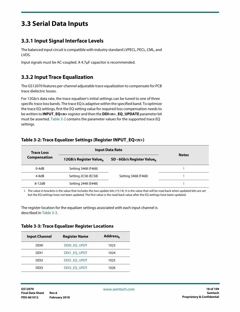
3.3.2 Input Trace EqualizationThe GS12070 features per-channel adjustable trace equalization to compensate for PCB trace dielectric losses.
For 12Gb/s data rate, the trace equalizer's initial settings can be tuned to one of three specific trace loss bands. The trace EQ is adaptive within the specified band. To optimize the trace EQ settings, first the EQ setting value for required loss compensation needs to be written to INPUT_EQ<n> register and then the DDI<n>_EQ_UPDATE parameter bit must be asserted. Table 3-2 contains the parameter values for the supported trace EQ settings.
The register location for the equalizer settings associated with each input channel is described in Table 3-3.
Table 3-2: Trace Equalizer Settings (Register INPUT_EQ<n>)
Trace Loss Compensation
Input Data RateNotes
12GB/s Register Valueh SD - 6Gb/s Register Valueh
0-4dB Setting 3468 (F468)
Setting 3468 (F468)
1
4-8dB Setting 2C58 (EC58) 1
8-12dB Setting 2448 (E448) 1
1. The value in brackets is the value that includes the two update bits (15:14). It is the value that will be read back when updated bits are set but the EQ settings have not been updated. The first value is the read-back value after the EQ settings have been updated.
Table 3-3: Trace Equalizer Register Locations
Input Channel Register Name Addressh
DDI0 DDI0_EQ_UPDT 1023
DDI1 DDI1_EQ_UPDT 1024
DDI2 DDI2_EQ_UPDT 1025
DDI3 DDI3_EQ_UPDT 1026
GS12070Final Data Sheet Rev.6PDS-061012 February 2018
18 of 109Semtech
Proprietary & Confidential
www.semtech.com

3.3.3 Input Signal PresentEach input has an associated active LOW control input pin called ISP which needs to be driven LOW when a valid input signal is applied. When a valid input signal is not present, this signal is to be driven HIGH.
The ISP_REG register can also be used to control this signal as well as change its polarity and report on the state of the ISP[3:0] input pin.
An example of how to use this pin in the application is to connect it to the lock pin of a reclocker that drives the respective serial input.
In the DeMUX mode, it is recommended to leave the associated ISP<n> HIGH for inputs that are not used.
3.3.4 Input Power-DownInputs that are not intended to be used can be powered down through the host interface. The DDI_PWR_DOWN registers provide per-lane control of the power down options.
3.4 Serial Data OutputsThe GS12070 has four serial digital differential data outputs capable of operating at SDI nominal rates of:
• 12G (11.88Gb/s, and 11.88/1.001Gb/s)
• 6G (5.94Gb/s and 5.94/1.001Gb/s)
• 3G (2.97Gb/s and 2.97/1.001Gb/s)
• HD (1.485Gb/s and 1.485/1.001Gb/s,)
• SD (270MHz)
Each output has a driver capable of driving a 100Ω differential load.
3.4.1 DDO Output SwingThe output swing is set to 400mVpp differential by default.
The swing can be changed by setting the DDO<n>_AMP parameter in the DDO_DRV_AMP register, as shown in Table 3-4. Once the value is set to the desired amplitude value for the selected output, set the DDO<n>_DRV_AMP_UPDATE parameter HIGH for this value to be loaded into the GS12070.
GS12070Final Data Sheet Rev.6PDS-061012 February 2018
19 of 109Semtech
Proprietary & Confidential
www.semtech.com

3.4.2 Output IdleSerial outputs can be individually set to Idle. When an output is set to Idle, its voltage will be set to the common mode voltage. These functions are programmed through DDO_IDLE register.
3.4.3 Output Power-DownOutputs that are not intended to be used can be powered down through the host interface. The OUTPUT_PWR_DOWN register provides per-lane control of the power down options.
The OUTPUT_PWR_DOWN register contains 16 bits, which can be broken down into four groups of four bits each. Each bit in the group of four bits is assigned to a DDO<n> output. Thus there are multiple bits required to power down a particular DDO<n> output. The power-down bit assigned to a DDO<n> output in each four-bit group must be the same.
Shown in Table 3-6 is an example of the value that is written to enable DDO0 and DDO2, but disable DDO1 and DDO3. For convenience, Table 3-5 is showing the HEX register value for all possible combinations of output power down.
Table 3-4: Output Swing Settings
DDO<n>_AMP Valueh
Nominal DDO Amplitude (mVpp diff )
0 400
1 500
2 600
3 700
4 800
5 900
6 1000
7 400
GS12070Final Data Sheet Rev.6PDS-061012 February 2018
20 of 109Semtech
Proprietary & Confidential
www.semtech.com

DDO3
1
f
Table 3-5: DDO<n> Power-Down ControlNote: Powered down output lanes denoted as PD.
Register Value
DDO Lane 0
DDO Lane 1
DDO Lane 2
DDO Lane 3
0000 Active Active Active Active
1111 Active Active Active PD
2222 Active Active PD Active
3333 Active Active PD PD
4444 Active PD Active Active
5555 Active PD Active PD
6666 Active PD PD PD
7777 Active PD PD PD
8888 PD Active Active Active
9999 PD Active Active PD
AAAA PD Active PD Active
BBBB PD Active PD PD
CCCC PD PD Active Active
DDDD PD PD Active PD
EEEE PD PD PD Active
FFFF PD PD PD PD
Table 3-6: Example of Register Value Required to Power Down DDO1 and DDO3
OUTPUT_PWR_DOWN
Bit Slice[15:12] [11:8] [7:4] [3:0]
DDO<n> Power Down
Bit AssignmentDDO0 DDO1 DDO2 DDO3 DDO0 DDO1 DDO2 DDO3 DDO0 DDO1 DDO2 DDO3 DDO0 DDO1 DDO2
Register Bit Value 0 1 0 1 0 1 0 1 0 1 0 1 0 1 0
Register Hex Value 5 5 5 5
GS12070Final Data Sheet Rev.6PDS-061012 February 2018
21 of 109Semtech
Proprietary & Confidential
www.semtech.com

3.4.4 Output Driver DisableThe serial output driver can be disabled. This feature can be used in combination with Output Power Down to realize additional power savings as the output driver is shut down.
This function can be programmed through the DDO_DRIVER_DISABLE Register.
3.5 Reference ClockThe GS12070 operates from a single reference clock. It is recommended to use a crystal with ±30ppm frequency tolerance and has a -40°C to +85°C temperature rating or better.
Please see 5.1 Typical Application Circuit for recommended crystal connection.
A differential clock can also be connected in place of the crystal. The quality of this reference clock must be equivalent or better than the crystal as it will impact output jitter. The differential clock must be AC coupled using a 10nF capacitor.
3.5.1 DDI CDR Reference Clock Configuration The GS12070 DDI CDR quad has two configuration options for high-speed clock generation from the reference clock.
The default DDI CDR configuration (on power-up) has slightly lower power consumption than the alternative CDR configuration, but the alternative CDR configuration is superior in jitter performance, IJT and power noise immunity to the default one.
The alternative CDR configuration can be selected in the initialization process after the power-up by writing a few registers. For more information please see the Application Note “GS12070 - Reducing jitter with different DDI CDR clocking configurations.”
Table 3-7: Reference Clock Configuration Selection
Reference Clock Configuration
Selection REFCLK_SEL[1:0]
XTAL_IN/OUT Reference Clock Frequency
00 Crystal 27MHz
01 Differential Clock 27MHz
10Not Supported
11
GS12070Final Data Sheet Rev.6PDS-061012 February 2018
22 of 109Semtech
Proprietary & Confidential
www.semtech.com

3.6 Digital I/OThe digital I/O pins must be interfaced at 1.8V LVCMOS logic levels.
3.7 Modes of OperationThe GS12070 operates in three distinctive modes:
• MUX (Multiplex)
• DeMUX (De-Multiplex)
• Bypass (Input to Output)
3.7.1 Operating Mode SelectionThe pins, MUX/DEMUX, and BYPASS configure the operating mode of the device.
In BYPASS mode, the device automatically searches for the data-rates, 12G, 6G, 3G, and HD at the input. Operation at SD (270Mb/s) must be manually set using the SD_BYPASS pin. This selection is available per lane and only active when the device is in BYPASS mode. When BYPASS mode is selected, the MUX/DEMUX pin is ignored.
The settings for mode selection are described in Table 3-8. The default pin settings for the GS12070 mode selection is set to DeMUX mode through a pull-down resistor. Alternatively, mode selection can be set through the OPEARTING_MODE_SEL_REG registers in the CSR.
Note: Register control of the MUX_DEMUX, MODE_SEL, PID_MODE and BYPASS parameters are grouped. All three functions must either be pin controlled or register controlled through REG_CTRL_OP_MODE_EN.
Table 3-8: Operating Mode Selection
PinMode
MUX/DEMUX BYPASS SD_BYPASS
0 0 0 DeMUX
1 0 0 MUX
X 1 0 Bypass
X 1 1SD Bypass (only available
when BYPASS = 1)
GS12070Final Data Sheet Rev.6PDS-061012 February 2018
23 of 109Semtech
Proprietary & Confidential
www.semtech.com

3.8 Input Serial Receiver and Input Processing Operation
3.8.1 Input Data RateThe data rate at the input is automatically configured when a specified MUX or DeMUX mode is selected. The maximum data rate supported for each DDI<n> input is shown in Table 3-9.
In the case of the BYPASS mode, the device by default searches for the data-rates, 12G, 6G, 3G, and HD at the input. If a valid SDI signal is found, and lock is achieved, the data rate will be reported (per input) in the parameters within the DATA_RATE_REPORT register as a two bit value. Table 3-10 describes the reported data rates and their parameter values. Note that SD is not reported as it must be set manually.
In BYPASS mode, the SD rate is not automatically detected and must be manually set for each individual input. This can be achieved by asserting the SD_BYPASS[3:0] pins or through the host interface using the SD_BYPASS_SEL_REG register.
The automatic data rate detection can be overridden and can be manually set through the MANUAL_RATE register. A parameter is available for each individual input. Table 3-10 applies for both reported data rate and the manual setting of the data rate.
Table 3-9: Serial Data Input Supported Data Rates
InputMODE
MUX DEMUX BYPASS
DDI0
—
6Gb/s
3Gb/s
1.5Gb/s
—
12Gb/s
6Gb/s
3Gb/s
—
—
12Gb/s
6Gb/s
3Gb/s
1.5Gb/s
270Mb/s
DDI1
—
6Gb/s
3Gb/s
1.5Gb/s
—
—
—
—
—
—
12Gb/s
6Gb/s
3Gb/s
1.5Gb/s
270Mb/s
DDI2
—
6Gb/s
3Gb/s
1.5Gb/s
—
12Gb/s
6Gb/s
3Gb/s
—
—
12Gb/s
6Gb/s
3Gb/s
1.5Gb/s
270Mb/s
DDI3
—
6Gb/s
3Gb/s
1.5Gb/s
—
—
—
—
—
—
12Gb/s
6Gb/s
3Gb/s
1.5Gb/s
270Mb/s
GS12070Final Data Sheet Rev.6PDS-061012 February 2018
24 of 109Semtech
Proprietary & Confidential
www.semtech.com

3.8.2 Input Loop BandwidthThe loop bandwidth of the input is individually configured on a per channel basis. The default loop bandwidth is optimized and it is not recommended that this value be changed.
There may be specific cases where the input loop bandwidth needs adjustment. This can be set through the DDI_CDR_LBW.
SeeTable 3-11 for CDR LBW settings.
Table 3-10: Data Rate Register Values for Setting and Reporting
Nominal Data Rate
Register Valueb
12G 11
6G 10
3G 01
HD 00
Table 3-11: CDR Bandwidth Settings
Data Rate CDR Bandwidth Bandwidth (MHz) CDR Lock to Data Time (μs)
12Gb/s
Low 3.26 5.2
Recommended 4.88 4.4
High 5.58 4.1
6Gb/s
Low 1.22 9.3
Recommended 1.63 7.6
High 4.88 4.4
3Gb/s
Low 0.61 18.6
Recommended 0.81 15.3
High 2.44 8.7
1.5Gb/s
Low 0.31 37.1
Recommended 0.41 30.6
High 1.22 17.5
GS12070Final Data Sheet Rev.6PDS-061012 February 2018
25 of 109Semtech
Proprietary & Confidential
www.semtech.com

3.8.3 Automatic Skew ToleranceThe GS12070 automatically adjusts for skew between multi-link inputs. Table 3-12 lists the maximum skew supported for the various MUX/DeMUX modes.
3.8.4 Status ReportingThe GS12070 has status monitoring of the following parameters
• LOCK
• PID ERROR
• PID DETECTED
• TRS ERROR
• CRC ERROR
• DATA RATE
• INTERLEAVED INPUT STREAM
Table 3-13 describes the parameter and the register that reports that parameter.
Table 3-12: Input Skew Compensation
Mode Conversion Time of Skew
DL 6Gb/s SL 12Gb/s
DL 3Gb/s SL 6Gb/s
DL 1.5Gb/s SL 3Gb/s
800ns
800ns
1600ns
QL 3Gb/s SL 12Gb/s
QL 3Gb/s SL 6Gb/s
QL 1.5Gb/s SL 6Gb/s
800ns
800ns
1600ns
DL 6Gb/s QL 3Gb/s 800ns
DL 12Gb/s QL 6Gb/s
QL 6Gb/s DL 12Gb/s
400ns
400ns
GS12070Final Data Sheet Rev.6PDS-061012 February 2018
26 of 109Semtech
Proprietary & Confidential
www.semtech.com

Figure 3-4: Input Data Stream Paths
Table 3-13: Input Status Reporting Parameters
Reporting Parameter
Register Name Description STAT Output Pin Availability
LOCKINPUT_
LOCK_REG
Asserts when the input has locked to the input data rate and detect three TRS sequences within a 2.5 line window.
LOCK is available for each individual input
STAT[15:12] - DDI 3
STAT[11:8] - DDI 2
STAT[7:4] - DDI 1
STAT[3:0] - DDI 0
Assignment to STAT pin is set through STAT_CH[3:0] registers
PID ERROR PID_ERROR
Asserts when the PID embedded in the input stream does not match the expected PID value.
PID ERROR Indication is available for each of the individual data streams and for each individual input.
PID DETECTEDPID_
DETECTED
Asserts when the PID is inserted in the input stream.
PID DETECTED Indication is available for each of the individual data streams and for each individual input.
TRS ERROR NA
Asserts when the received TRS's protection bit is incorrect.
TRS_PERR indication is available or each of the individual data streams and for each individual input.
CRC ERROR CRC_ERRORAsserts when a CRC error has been detected at inputs. This register is a logical OR of each DDI CRC error, if detected.
NADATA RATE
DATA_RATE_REPORT
Indicates the data rate on the DDI[3:0] inputs, two bits per input.
INTERLEAVED INPUT STREAM
VID_STREAM_INTERLEAVED_
STAT
Indicates that the input video stream is interleaved when HIGH.
One bit per stream, two streams per input.
Note: See Figure 3-4: Input Data Stream Paths.
VideoProcessing
Rx
Rx
Rx
Rx
DDI0
DDI1
DDI2
DDI3
DDI0_DS1
DDI0_DS2
DDI1_DS1
DDI1_DS2
DDI2_DS1
DDI2_DS2
DDI3_DS1
DDI3_DS2
GS12070Final Data Sheet Rev.6PDS-061012 February 2018
27 of 109Semtech
Proprietary & Confidential
www.semtech.com

3.9 Serial Transmitter Operation
3.9.1 Output Assignment
3.9.1.1 Default Output Assignments
Default output assignments are configured per mode as listed in Table 3-14.
3.9.1.2 Manual Output Assignment
Each output can be assigned to:
• Multiplexed streams in MUX mode (M0 or M1 processed output)
• Demultiplexed streams in DeMUX mode (DM0 or DM1 processed output)
• Any of the four input channels
This feature is available in any mode, regardless of the default assignment of the serial output. Assignment of the output is configured through the OUTPUT_ASGMT_ DDO<n> and enabled through the REG_CTRL_OUTPUT_ASGMT_EN register.
Table 3-14: Serial Tx Output Assignment
Mode Tx0 Tx1 Tx2 Tx3 Notes
MUX
QL3GSL12G M0 M0 (DDO idle) M0 (DDO idle) M0 (DDO idle) —
QLHDSL6G M0 M0 (DDO idle) M0 (DDO idle) M0 (DDO idle) —
QL6GDL12G M0 M0 (DDO idle) M1 M1 (DDO idle) —
QL3GDL6G M0 M0 (DDO idle) M1 M1 (DDO idle) —
DL6GSL12G M0 M0 (DDO idle) M1 M1 (DDO idle) 1
DL3GSL6G M0 M0 (DDO idle) M1 M1 (DDO idle) 1
DLHDSL3G M0 M0 (DDO idle) N/A N/A —
DeMUX
SL12GQL3G DM0 DM0 DM0 DM0 —
SL6GQLHD DM0 DM0 DM0 DM0 —
DL12GQL6G DM0 DM0 DM1 DM1 —
DL6GQL3G DM0 DM0 DM0 DM0 —
SL12GDL6G DM0 DM0 DM1 DM1 2
SL6GDL3G DM0 DM0 DM1 DM1 2
SL3GDLHD DM0 DM0 N/A N/A —
1. Tx2(M1path) is powered down by default. To use Tx2(M1 path) as a secondary link it must be enabled manually via SEC_LINK_ENABLE pin or through the CSR. See Figure 3-7 and Section 3.10.2 for further details.
2. Tx2(DM1 path) and Tx3(DM1path) are powered down by default. To use Tx2(DM1 path) and Tx3(DM1 path) as a secondary link they must be enabled manually via SEC_LINK_ENABLE pin or through the CSR. See Figure 3-10 and Section 3.11.2 for further details.
GS12070Final Data Sheet Rev.6PDS-061012 February 2018
28 of 109Semtech
Proprietary & Confidential
www.semtech.com

Note: Custom output assignments will be retained, even if the mode is changed. To return to the default output assignment, the register REG_CTRL_OUTPUT_ASGMT_EN should be set back to “0”.
Figure 3-5: Output Assignment Selection
3.9.2 Output Loop BandwidthThe loop bandwidth of the output is individually configured on a per output basis. The default loop bandwidth should be configured based on the requirements of the device connected to the DDO[3:0] serial outputs.
The loop bandwidth can be set through the DDO_LBW register and will take effect when the DDO_LBW_UPDT register has been written to. Please refer to Table 3-15.
M0 Processed Output
M1 Processed Output
DDO<n>
000
111
DM0_DDO<n>
DM1_DDO<n>
DDI0
DDI1
DDI2
DDI3
OUTPUT_ASGMT_DDO<n>
Table 3-15: DDO Loop Bandwidth Setting
DDO_LBW_SETTINGSh
12G LBW (MHz)
6G LBW (MHz)
3G LBW (MHz)
1.5G LBW (MHz)
0 RSVD
1 0.13 0.13 0.13 0.13
2 0.25 0.25 0.25 0.25
3 0.5 0.5 0.5 0.5
4 1.01 1.01 1.01 1.01
5 2.01 2.01 2.01 2.01
6 4.03 4.03 4.03 2.01
7 8.06 8.06 8.06 2.01
8 16.11 16.11 8.06 2.01
9 32.33 16.11 8.06 2.01
A to F RSVD
GS12070Final Data Sheet Rev.6PDS-061012 February 2018
29 of 109Semtech
Proprietary & Confidential
www.semtech.com

3.9.3 Transmitter Input Clock SelectionBy default, the Tx PLL input clock is selected by the internal control block from the receiver's extracted clocks.
In the MUX or DeMUX mode of operation, the following receiver's clocks will be selected:
• RX0_CLK (from DDI0 input) — if M0 or DM0 data are selected as input to the transmitter (all QLSL, QLDL muxing/demuxing modes and DLSL modes for M0/DM0 paths)
• RX2_CLK (from DDI2 input) — if M1 or DM1 data are selected as input to the transmitter (DLSL modes for M1/DM1 paths)
In Bypass Mode, the Tx PLL input clock is taken from the receiver (DDI input) which is connected to the transmitter.
Tx<n> PLL clock selection can be changed through TX_REF_CLK_SEL register. Selection is enabled by TX_REF_CLK_CTLR[n] parameter and a clock source is selected through TX<n>_REF_CLK_SEL parameter.
Additionally an external clock from the pins TX_PCLK0 and TX_PCLK01 can be selected as the Tx<n> PLL clock input through the register TX_EXT_REF_CLK_SEL. The external clock is selected through TX<n>_EXT_REF_CLK_EN and the parameter TX0_EXT_REF_CLK_SEL selects between clocks from and TX_PCLK0 and TX_PCLK1.
Note: The external clock has to be frequency locked to the input data.
Figure 3-6: Tx PLL Input Clock Selection Block
3.10 Multiplex Mode
3.10.1 Conversion SelectionIn MUX mode, conversion modes are illustrated in Figure 3-7.
The conversion mode can be set through the MODE_SEL[2:0] pins.
TX_REF_CLK_CTLR[n]
TX<n>_REF_CLK_INTERNAL_SEL[1:0]
TX<n>_REF_CLK_SEL[1:0]
TX<n>_EXT_REF_CLK_EN
TX<n>_PCLK
TX<n>_EXT_REF_CLK_SEL
TX<n>_PCLK_EXT
TX<n>_PCLK_INT
RX0_CLK
RX1_CLKRX2_CLKRX3_CLK
TC_PCLK0pin
TC_PCLK1pin
0
1
00
11
0
1
0
1
GS12070Final Data Sheet Rev.6PDS-061012 February 2018
30 of 109Semtech
Proprietary & Confidential
www.semtech.com

The OPERATING _MODE_SEL _REG register can also be used to select the conversion mode and override the pin settings. The MODE_SEL parameter is used to set the mode and the REG_CTRL_MODE_SEL_EN parameter is used to enable the pin override.
The mode selection settings are listed in Table 3-16.
Figure 3-7: Multiplex Conversion Modes
Table 3-16: MUX Mode Up Conversion
Pins MUX Mode Notes(Refer to
Figure 3-7)MUX/DEMUX MODE_SEL2 MODE_SEL1 MODE_SEL0 Input Output
1 1 1 1 QL 3Gb/s SL 12Gb/s (a)
1 1 1 0 QL 1.5Gb/s SL 6Gb/s (b)
1 1 0 1 QL 6Gb/s DL 12Gb/s (c)
1 1 0 0 QL 3Gb/s DL 6Gb/s (d)
1 0 1 1 DL 6Gb/s SL 12Gb/s (e)
1 0 1 0 DL 3Gb/s SL 6Gb/s (f )
1 0 0 1 DL 1.5Gb/s SL 3Gb/s (g)
1 0 0 0 RSVD RSVD —
(b)
(d)
(f)
(g)
(c)
(e)
(a)
3Gb/s 12Gb/s
3Gb/s
3Gb/s
3Gb/s
6Gb/s1.5Gb/s
1.5Gb/s
1.5Gb/s
1.5Gb/s
6Gb/s
6Gb/s
6Gb/s
6Gb/s
12Gb/s
12Gb/s
3Gb/s
3Gb/s
3Gb/s
3Gb/s
6Gb/s
6Gb/s
6Gb/s
6Gb/s
6Gb/s
12Gb/s
12Gb/s
6Gb/s3Gb/s
3Gb/s
1.5Gb/s
1.5Gb/s
3Gb/s
The system accepts quad 3Gb/s input signals and drives a single link 12Gb/s output signal. The 12Gb/s signal is outputted from DDO0 by default but can be set to output from any pin.
The system accepts quad 1.5Gb/s input signals and drives a single link 6Gb/s output signal. The 6Gb/s signal is outputted from DDO0 by default but can be set to output from any pin.
The system accepts quad 6Gb/s input signals and drives 12Gb/s dual link output signals.The 12Gb/s signals are outputted from DDO0 and DDO2 by default, but can be set to output from any pin.
The system accepts quad 3Gb/s input signals and drives dual link 6Gb/s output signals. The 6Gb/s signals are outputted from DDO0 and DDO2 by default, but can be set to output from any pin.
The system accepts two independent dual link 6Gb/s input signals and drives two single link 12Gb/s output signals. The 12Gb/s signals are outputted from DDO0 and DDO2 by default, but can be set to output from any pins.
The system accepts two independent dual link 3Gb/sinput signals and drives two single link 6Gb/s output signals. The 6Gb/s signals are outputted from DDO0 and DDO2 by default, but can be set to output from any pins.
The system accepts dual link 1.5Gb/s input signals on DDI0 and DDI1 inputs and drives single link 3Gb/s output signals. The 3Gb/s signals is outputtedfrom DDO0 by default , but can be set to output from any pins.
QL3G → SL12G
QL6G → DL12G
2x DL6G → 2x SL12G
6Gb/s 6Gb/s3Gb/s
3Gb/s
QLHD → SL6G
QL3G → DL6G
2x DL3G → 2x SL6G
DLHD → SL3G
GS12070Final Data Sheet Rev.6PDS-061012 February 2018
31 of 109Semtech
Proprietary & Confidential
www.semtech.com

Note:
• In Figure 3-7 e) and f ), solid coloured inputs use path M0 and gradient coloured inputs use path M1. See Section 3.10.2 for further details.
• In order to enable DL 1.5Gb/s to SL 3Gb/s conversion, it is required to set additional registers (See Table 3-17).
3.10.2 Multiplexing PathsThe MUX modes will enable one of two paths based on the selected conversion mode.
For quad link inputs the M0 path is used.
For dual link inputs both M0 and M1can be used based on the application requirement. By default M1 is powered down. To enable the M1 path, the pin SEC_LINK_ENABLE should be driven HIGH.
Alternatively, the parameter SEC_LINK_REG within the OPERATING_MODE_SEL_REG register can be used. The parameter REG_CTRL_SEC_LINK_EN is used to override the pin control and enable the register selection of this feature.
Figure 3-8: Multiplexing Paths
Table 3-17: DL 1.5Gb/s to SL 3Gb/s conversion
Addressh Datah
16 3
13 1
65 92
64 2D48
DDI0
DDI1 M0PROCESSEDOUTPUT
VirtualInterface UHD
MUX
Mux M0
Mux M1
M1PROCESSEDOUTPUT
V0DDI2DDI3
VirtualInterface UHD
MUXV1
GS12070Final Data Sheet Rev.6PDS-061012 February 2018
32 of 109Semtech
Proprietary & Confidential
www.semtech.com

3.10.3 SMPTE CompatibilityTable 3-18 outlines the conversion mappings that are compatible to the SMPTE UHD standards.
If PID_MODE pin is set to ‘1’ the input streams will be multiplexed according to the mappings defined by the SMPTE UHDTV standards. The payload identifiers will be passed to the output unchanged, as received. The Payload ID can be inserted manually, if required.
The Payload ID will not be inserted for the DL 1.5Gb/s to SL 3Gb/s conversion regardless of the PID_MODE pin setting. For the DL 1.5Gb/s to SL 3Gb/s conversion, the user needs to manually insert PIDs.
Note: For QL Level B mapping, the device will not convert input from Level B mapping to a Level A mapping. QL Level B streams will be multiplexed as DS8-DS4-DS6-DS2-DS7-DS3-DS5-DS1. The SL12G output will not be compatible with a SL12G input that has been mapped per ST2081-11 2160-line Mode 1. A second GS12070 can be used to demultiplex SL12G mapped data streams in QL3G Level B mapping.
3.10.4 Lost InputIn MUX mode, if the GS12070 fails to detect LOCK on an input, the primary input is copied to the missing input(s). By default, DDI0 is the primary channel. This function is enabled on all inputs.
The LOST_INPUT _IGNORE_CTRL register allows for customization of this feature.
Table 3-18: MUX Mode SMPTE Compatibility
MUX Mode Supported SMPTE Mapping
Input Output Input Mapping Output Mapping
QL 1.5Gb/s SL 6Gb/s ST274 – 30/25/24 FR, progressive ST2081-10 2160-line Mode 1
DL 3Gb/s SL 6Gb/s
ST425-3 1080-line Level A Mapping
ST425-3 1080-line Level B DL Mapping
ST425-3 2160-line Mapping
ST2081-10 1080-line Mode 2
—
ST2081-10 2160-line Mode 1
QL 3Gb/s DL 6Gb/sST425-5 2160-line Level A Mapping
ST425-5 2160-line Level B Mapping
ST2081-11 2160-line Mode 1
See Note below
QL 3Gb/s SL 12Gb/sST425-5 2160-line Level A Mapping
ST425-5 2160-line Level B Mapping
ST2082-10 2160-line Mode 1
See Note below
DL 6Gb/s SL 12Gb/sST2081-11 2160-line Mode 1
ST2081-11 1080-line Mode 2
ST2082-10 2160-line Mode 1
ST2082-10 1080-line Mode 2
QL 6Gb/s DL 12Gb/sST2081-12 4320-line Mode 1
ST2081-12 2160-line Mode 2
ST2082-11 4320-line Mode 1
ST2082-11 2160-line Mode 2
GS12070Final Data Sheet Rev.6PDS-061012 February 2018
33 of 109Semtech
Proprietary & Confidential
www.semtech.com

The primary input to be re-defined, can be configured through the M0_PRIM_CH parameter for Quad-Link inputs and Dual-Link inputs appearing on DDI1:0]. For Dual-Link inputs appearing on DDI[3:2] this feature is not supported.
The feature can be disabled on a per-input basis through the IGNORE_LOST_INPUT parameter.
3.10.5 Automatic Input Link OrderingThe SMPTE multi-link standards, define the Link numbers within Byte 4 of the SMPTE ST 352M Payload ID.
By default, the GS12070 will associate the Link number with the respective DDI<n> input:
• Input on DDI0 is treated as Link 1
• Input on DDI1 is treated as Link 2
• Input on DDI2 is treated as Link 3
• Input on DDI3 is treated as Link 4
The GS12070 can use the Payload ID to identify the Link number and disassociate the Link number with the DDI<n> inputs and multiplex the Input in the correct SMPTE defined order. To enable this function, the LINK_ASGMT pin must be set to logic HIGH. Alternatively this can be set through the VI_ASGMT_0 register using the LNK_ASGMT_SEL parameter. The parameter REG_CTRL_LNK _ASGMT_SEL_EN can be used to override the pin setting.
3.10.6 MUX Manual Input Channel AssignmentIn cases where the PID is not defined, incorrect, or missing, the input can be manually rearranged into the UHD multiplexer. The virtual interface allows manual reassignment of an input.
Manual input assignment can be enabled through the parameter MANUAL_CTRL_LNK_ASGMT parameter in the VI_ASGMT_0 register for M0 and M1 path.
For the M0 path, VI0_CH<n>_SEL parameter can be used to select which input is assigned to each channel container.
For the M1 path, VI1_CH<n>_SEL parameter can be used to select which input is assigned to each channel container.
GS12070Final Data Sheet Rev.6PDS-061012 February 2018
34 of 109Semtech
Proprietary & Confidential
www.semtech.com

Figure 3-9: Virtual Interface
3.11 Demultiplex Mode
3.11.1 Conversion SelectionIn DeMUX mode, conversion modes are illustrated in Figure 3-10.
The conversion mode can be set through the MODE_SEL[2:0] pins. The OPERATING _MODE_SEL _REG register can also be used to select the conversion mode and override the pin settings. The MODE_SEL parameter is used to set the mode and the REG_CTRL_MODE_SEL_EN parameter is used to enable the pin override.
The mode selection settings are listed in Table 3-19.
DDI0DDI1
To UHDMUX0
DDI2DDI3
VI0_CH0_SEL
CH0_DS1
CH0_DS2
CH1_DS1
CH1_DS2
CH2_DS1
CH2_DS2
CH3_DS1
CH3_DS2
DDI0DDI1DDI2DDI3
VI0_CH1_SEL
DDI0DDI1DDI2DDI3
VI0_CH2_SEL
DDI0DDI1DDI2DDI3
VI0_CH3_SEL
VI_DS1
VI_DS2
VI_DS3
VI_DS4
VI_DS5
VI_DS6
VI_DS7
VI_DS8
InputProcessing
InputProcessing
InputProcessing
InputProcessing
DDI1
DDI2
DDI0
DDI3
CH2_DS1
CH2_DS2
CH3_DS1
CH3_DS2
VI_DS1
VI_DS2
VI_DS3
VI_DS4
DDI2DDI3
DDI2DDI3
VI1_CH0_SEL
VI1_CH1_SELTo UHDMUX1
Virtual Interface V0
Virtual Interface V1
GS12070Final Data Sheet Rev.6PDS-061012 February 2018
35 of 109Semtech
Proprietary & Confidential
www.semtech.com

Figure 3-10: DeMUX Conversion Modes
Note: In Figure 3-10 e) and f), solid coloured inputs use path DM0 and gradient coloured inputs use path DM1. See Section 3.11.2 for further details.
Table 3-19: DeMUX Mode Down Conversion
Pins DeMUX Mode Notes(Refer to
Figure 3-10)MUX/DEMUX MODE_SEL2 MODE_SEL1 MODE_SEL0 Input Output
0 1 1 1 SL 12Gb/s QL 3Gb/s (a)
0 1 1 0 SL 6Gb/s QL 1.5Gb/s (b)
0 1 0 1 DL 12Gb/s QL 6Gb/s (c)
0 1 0 0 DL 6Gb/s QL 3Gb/s (d)
0 0 1 1 SL 12Gb/s DL 6Gb/s (e)
0 0 1 0 SL 6Gb/s DL 3Gb/s (f )
0 0 0 1 SL 3Gb/s DL 1.5Gb/s (g)
0 0 0 0 RSVD RSVD —
(a)
12Gb/s
3Gb/s
3Gb/s
3Gb/s
3Gb/s
(b)
1.5Gb/s
1.5Gb/s
1.5Gb/s
1.5Gb/s
6Gb/s
(c)
6Gb/s
6Gb/s
6Gb/s
6Gb/s
12Gb/s
12Gb/s
(d)
3Gb/s
3Gb/s
3Gb/s
3Gb/s6Gb/s
6Gb/s
(e)
12Gb/s
12Gb/s
6Gb/s
6Gb/s
(g)
3Gb/s 1.5Gb/s
1.5Gb/s
3Gb/s
3Gb/s
6Gb/s
(f)
The system accepts a single link 12Gb/s inputsignal and drives quad link 3Gb/s output signals.The 12Gb/s signal is input into DDI0 by default. This can be changed to DDI2 through the secondary link assignment feature.
The system accepts a single link 6Gb/s inputsignal and drives quad link 1.5Gb/s output signals.The 6Gb/s signal can only be inputted into DDI0.
The system accepts dual link 12Gb/s inputsignals and drives quad link 6Gb/s output signals.The 12Gb/s signals can only be inputted into DDI0 and DDI2.
The system accepts dual link 6Gb/s inputsignals and drives quad link 3Gb/s output signals.The 6Gb/s signals can only be inputted into DDI0 and DDI2.
The system accepts two independent single link 12Gb/s input signals and drives two dual link 6Gb/s output signals. The 12Gb/s signals can only be inputted into DDI0 and DDI2.
The system accepts two independent single link 6Gb/s input signals and drives two dual link 3Gb/s output signals. The 6Gb/s signals can only be inputted into DDI0 and DDI2.
The system accepts a single link 3Gb/s input signal anddrives two dual link 1.5Gb/s output signals. The 1.5Gb/sare assigned to DDO0 and DDO1 by default but can beassigned to other two outputs as well.
6Gb/s
6Gb/s 6Gb/s
3Gb/s
3Gb/s
SL12G → QL3G
DL12G → QL6G
12Gb/s
SL6G → QLHD
2x SL12G → 2x DL6G
DL6G → QL3G
2x SL6G → 2x DL3G
SL3G → DLHD
GS12070Final Data Sheet Rev.6PDS-061012 February 2018
36 of 109Semtech
Proprietary & Confidential
www.semtech.com

3.11.2 Demultiplexing PathsThe DeMUX modes will enable one of two paths based on the selected conversion mode.
For quad link outputs the DM0 path is used.
For dual link outputs both DM0 and DM1can be used based on the application requirement. By default DM1 is powered down. To enable DM1, the pin SEC_LINK_ENABLE should be driven HIGH.
Alternatively, the parameter SEC_LINK_REG within the OPERATING_MODE_SEL_REG register can be used. The parameter REG_CTRL_SEC_LINK_EN is used to override the pin control and enable the register selection of this feature.
Figure 3-11: Demultiplexing Paths
DDI0DDI2
DM0PROCESSEDOUTPUT
UHDDeMUX
Prog.Delay
OutputLink
Assignment
UHDDeMUX
OutputLink
Assignment
DeMux DM0
DeMux DM1
DM1PROCESSEDOUTPUT
GS12070Final Data Sheet Rev.6PDS-061012 February 2018
37 of 109Semtech
Proprietary & Confidential
www.semtech.com

Figure 3-12: DL12G-QL6G Output Link Assignment
Note: Default setting for SEL_DM_DL12_VIR is "10" so that output assignment is:
DDO0 - Link3
DDO1 - Link4
DDO2 - Link1
DDO3 - Link2
Setting register 65h (DM_DL12_VIR) to 55h (SEL_DM_DL12_VIR to 01) will remap the output order to:
DDO0 - Link1
DDO1 - Link2
DDO2 - Link3
DDO3 - Link4
Inputprocessing,UHD DM1,
Output delay
DM1
Inputprocessing,UHD DM0,
Output delay
DM0
DM1_DS1DM1_DS3DM1_DS2DM1_DS4DM1_DS5DM1_DS7DM1_DS6DM1_DS8
DM0_DS1DM0_DS3DM0_DS2DM0_DS4DM0_DS5DM0_DS7DM0_DS6DM0_DS8
DDI0
DDI2
DM0_DS1DM0_DS3DM0_DS2DM0_DS4DM0_DS5DM0_DS7DM0_DS6DM0_DS8
DM1_DS1DM1_DS3DM1_DS2DM1_DS4DM1_DS5DM1_DS7DM1_DS6DM1_DS8
SEL_DM_DL12_VIR[0]
1
0
SEL_DM_DL12_VIR[1]
0
1 DM1_VIR
DM0_VIR
DM0_Link2
DM0_Link1
DM1_Link2
DM1_Link1
SEL_DM0_VIRT0
DM0_DDO0DM0_Link1
DM0_Link2
SEL_DM0_VIRT1
DM0_DDO1DM0_Link1
DM0_Link2
SEL_DM1_VIRT0
DM1_DDO2DM1_Link1
DM1_Link2
SEL_DM1_VIRT1
DM1_DDO3DM1_Link1
DM1_Link2
GS12070Final Data Sheet Rev.6PDS-061012 February 2018
38 of 109Semtech
Proprietary & Confidential
www.semtech.com

3.11.3 SMPTE CompatibilityTable 3-20 outlines the conversion mappings that are compatible to the SMPTE UHD standards.
If PID_MODE pin is set to ‘1’ the input streams will be demultiplexed according to the mappings defined by the SMPTE UHDTV standards. The payload identifiers will be passed to the output unchanged, as received. The Payload ID can be inserted manually, if required.
3.11.4 Lane DelayIn DeMUX mode, the delay between each output channel can be manually adjusted for up to:
• 6.8μs in 6.7ns increments for 3G and 6G outputs
• 13.8μs in 13.47ns increments for HD Outputs
The output delay can be enabled through the DM0_DELAY_EN register. Each of the delay increment steps can be set through the DM0_DELAY_LINK[3:0] parameters.
Note: When the delay block has been enabled, the latency is increased by two PCLK.
By default, each of the links appear on the respective DDO outputs:
• LINK0 appears on DDO0
• LINK1 appears on DDO1
• LINK2 appears on DDO2
• LINK3 appears on DDO3
Note: The DM0_delay block is located before the DeMUX Output Link Assignment block. If the manual output link assignment feature is used together with the lane delay, the link with the added delay will be remapped to the selected DDO.
Table 3-20: DeMUX Mode SMPTE Compatibility
DeMUX Mode Supported SMPTE Mapping
Input Output Input Mapping Output Mapping
SL 6Gb/s QL 1.5Gb/s ST2081-10 2160-line Mode 1 ST274 – 30/25/24 FR, progressive
SL 6Gb/s DL 3Gb/s
ST2081-10 1080-line Mode 2
ST2081-10 2160-line Mode 1
ST425-3 1080-line Level A Mapping
ST425-3 1080-line Level B DL Mapping
ST425-3 2160-line Mapping
SL 12Gb/s DL 6Gb/sST2082-10 2160-line Mode 1
ST2082-10 1080-line Mode 2
ST2081-11 2160-line Mode 1
ST2081-11 1080-line Mode 2
DL 12Gb/s QL 6Gb/s
ST2082-11 4320-line Mode 1
ST2082-11 2160-line Mode 2
ST-2082-11 2160-line Mode 3
ST2081-12 4320-line Mode 1
ST2081-12 2160-line Mode 2
ST2081-12 2160-line Mode 3
GS12070Final Data Sheet Rev.6PDS-061012 February 2018
39 of 109Semtech
Proprietary & Confidential
www.semtech.com

3.11.5 DeMUX Output Link AssignmentBy default, the SMPTE multilink outputs are mapped as follows:
The default output assignment can be custom defined. Manual output link assignment can be enabled through the parameter REG_CTRL_SEL_DM0_VIRT in the SEL_DM0_VIRT register for DM0 path.
For the DM1 path, the parameter REG_CTRL_SEL_DM1_VIRT in the SEL_DM1_VIRT register should be used.
For the DM0 path, SEL_DM0_VIRT<n> parameter can be used to select which link is assigned to each DDO Output.
For the DM1 path, SEL_DM1_VIRT<n> parameter can be used to select which input is assigned to each DDO Output.
Table 3-21: Default Output Assignment of Multilink Standards
Output Quad Link Outputs Dual Link Outputs
DDO0 Link 1 DM0 Link 1
DDO1 Link 2 DM0 Link 2
DDO2 Link 3 DM1 Link 1
DDO3 Link 4 DM1 Link 2
GS12070Final Data Sheet Rev.6PDS-061012 February 2018
40 of 109Semtech
Proprietary & Confidential
www.semtech.com

Figure 3-13: Output Link Assignment Selection
LINK1LINK2LINK3LINK4
SEL_DM0_VIRT0
LINK1LINK2LINK3LINK4
LINK1LINK2LINK3LINK4
LINK1LINK2LINK3LINK4
DM0_DS1
DM0_DS2
DM0_DS3
DM0_DS4
DM0_DS5
DM0_DS6
DM0_DS7
DM0_DS8
LINK1LINK2
LINK1LINK2
SEL_DM1_VIRT[0]
SEL_DM1_VIRT[1]
UHD_DM0,Prog. Delay
SEL_DM0_VIRT1
SEL_DM0_VIRT2
SEL_DM0_VIRT3
LINK1
LINK2
LINK3
LINK4
DM0_DDO0
DM0_DDO1
DM0_DDO2
DM0_DDO3
DM1_DS1
DM1_DS2
DM1_DS3
DM1_DS4
UHD_DM1
LINK1
LINK2
LINK1LINK2
LINK1LINK2
SEL_DM1_VIRT[2]
SEL_DM1_VIRT[3]
DM1_DDO0
DM1_DDO1
DM1_DDO2
DM1_DDO3
GS12070Final Data Sheet Rev.6PDS-061012 February 2018
41 of 109Semtech
Proprietary & Confidential
www.semtech.com

3.12 Bypass ModeIn bypass mode the GS12070 automatically bypasses 12Gb/s, 6Gb/s, 3Gb/s, and 1.5Gb/s video data from the input to the output.
The input to output assignment by default:
• DDI0 is assigned to DDO0
• DDI1 is assigned to DDO1
• DDI2 is assigned to DDO2
• DDI3 is assigned to DDO3
If required, any of the inputs can be assigned to any of the output using Output Assignment feature, Section 3.9.1.
Note: When the mode of operation is switched from the BYPASS mode to MUX/DeMUX mode and vice versa, the CORE_RESET (register RESET_1, 79h) bit has to be toggled. Alternatively, all the ISP pins can be toggled if there is no GSPI access or if preferred by the user.
3.12.1 Input Stream Data Rate DetectionIn bypass mode, when the input is 1.5G, 3G, 6G, or 12G, the GS12070 is able to automatically determine each input data rate and reported in DATA_RATE_REPORT register, in the parameters DATA_RATE_RX<n>.
The data rate can be set manually through the parameter REG_CTRL_MANUAL_RATE in the MANUAL_RATE register.
3.12.2 SD Bypass ModeThe device is capable of passing through signals serialized as per SMPTE 259 at 270Mb/s rate in SD Bypass mode only. SD Bypass mode is manually selectable on a per-channel basis and only available when BYPASS is set HIGH.
The SD_ BYPASS pin can be overwritten via the controls found in the SD_BYPASS_SEL_REG register.
When in the SD bypass mode, input data is oversampled. The default oversampling data rate is 3Gb/s. The oversampling introduces periodic jitter, with the p-p value proportional to the oversampling rate. The jitter can be reduced by increasing the oversampling rate to 6Gb/s. The oversampling rate can be set to 6Gb/s by setting SD_BYPASS_ RATE_6G_3Gb, parameter, register SD_BYPASS_ SEL_REG to 1.
3.12.3 PRBS Data BypassIn the data rate detection process, the data rate detection block searches for TRS data words in the input data stream. Hence, the GS12070 is able to automatically determine input data rate only if the input is SDI video. If the input is PRBS data, the GS12070 data rate has to be set manually to pass data.
GS12070Final Data Sheet Rev.6PDS-061012 February 2018
42 of 109Semtech
Proprietary & Confidential
www.semtech.com

In order to pass PRBS data, the following GS12070 registers need to be set:
• address = 6h (MANUAL_RATE) data = depends on the data rate (should always be written first)
The register MANUAL_RATE should be set as the following for the different data rates:
12G - FFFh
6G - AAFh
3G - 55Fh
HD - Fh
• address = 3h (INPUT_ LOCK_REG) data = FF0h - Input lock overwrite
• address = Ah (DDO_IDLE) data = F00h - Tx power down overwrite
• address = 8h (RSVD) data = F0h - Set internal ready signal HIGH (should always be written last)
3.13 Payload ID HandlingThe GS12070 will automatically detect and replace the appropriate PID based on the selected mode. PID handling can be disabled through the PID_MODE Pin or the PID_MODE parameter in the OPERATING _MODE_SEL _REG register.
Note: Register control of the MUX_DEMUX, PID_MODE and BYPASS are grouped. All three functions must either be Register controlled or pin controlled.
Note: PID handling is not available when the device is in the bypass mode.
3.13.1 Detection of Payload IDIf a Payload ID is detected in the incoming video input, it can be read through the CSR. Based on the input format,Table 3-22 through Table 3-25 describe the registers where the Payload ID is stored.
GS12070Final Data Sheet Rev.6PDS-061012 February 2018
43 of 109Semtech
Proprietary & Confidential
www.semtech.com

Table 3-22: DeMUX Mode DM0 Payload ID Detected Registers
Input Register SL12QL3 SL6QLHD DL12QL6 SL12DL6 DL6QL3 SL6DL3 SL6DLHD
DDI0
PID_DET_CH0A_DS1_* DDI0_DS1 DDI0_DS1 DDI0_DS1 DDI0_DS1 DDI0_DS1 DDI0_DS1 NA
PID_DET_CH0A_DS2_* DDI0_DS5 DDI0_DS3 DDI0_DS5 DDI0_DS5 DDI0_DS3 DDI0_DS3 NA
PID_DET_CH0B_DS1_* DDI0_DS3 DDI0_DS2 DDI0_DS3 DDI0_DS3 DDI0_DS2 DDI0_DS2 DDI0_DS1
PID_DET_CH0B_DS2_* DDI0_DS7 DDI0_DS4 DDI0_DS7 DDI0_DS7 DDI0_DS4 DDI0_DS4 DDI0_DS2
DDI1
PID_DET_CH1A_DS1_* DDI0_DS2 NA DDI0_DS2 DDI0_DS2 NA NA NA
PID_DET_CH1A_DS2_* DDI0_DS6 NA DDI0_DS6 DDI0_DS6 NA NA NA
PID_DET_CH1B_DS1_* DDI0_DS4 NA DDI0_DS4 DDI0_DS4 NA NA NA
PID_DET_CH1B_DS2_* DDI0_DS8 NA DDI0_DS8 DDI0_DS8 NA NA NA
DDI2
PID_DET_CH2A_DS1_* NA NA DDI2_DS1 NA DDI2_DS1 NA NA
PID_DET_CH2A_DS2_* NA NA DDI2_DS5 NA DDI2_DS3 NA NA
PID_DET_CH2B_DS1_* NA NA DDI2_DS3 NA DDI2_DS2 NA NA
PID_DET_CH2B_DS2_* NA NA DDI2_DS7 NA DDI2_DS4 NA NA
DDI3
PID_DET_CH3A_DS1_* NA NA DDI2_DS2 NA NA NA NA
PID_DET_CH3A_DS2_* NA NA DDI2_DS6 NA NA NA NA
PID_DET_CH3B_DS1_* NA NA DDI2_DS4 NA NA NA NA
PID_DET_CH3B_DS2_* NA NA DDI2_DS8 NA NA NA NA
Table 3-23: DeMUX Mode DM1 Payload ID Detected Registers
Input Register SL12QL3 SL6DL3
DDI2
PID_DET_CH2A_DS1_* DDI2_DS1 DDI2_DS1
PID_DET_CH2A_DS2_* DDI2_DS5 DDI2_DS3
PID_DET_CH2B_DS1_* DDI2_DS3 DDI2_DS2
PID_DET_CH2B_DS2_* DDI2_DS7 DDI2_DS4
DDI3
PID_DET_CH3A_DS1_* DDI2_DS2 NA
PID_DET_CH3A_DS2_* DDI2_DS6 NA
PID_DET_CH3B_DS1_* DDI2_DS4 NA
PID_DET_CH3B_DS2_* DDI2_DS8 NA
GS12070Final Data Sheet Rev.6PDS-061012 February 2018
44 of 109Semtech
Proprietary & Confidential
www.semtech.com

Table 3-24: MUX Mode M0 Payload ID Detected Registers
Input Register QL3SL12 QLHDSL6 QL6DL12 DL6SL12 QL3DL6 DL3SL6 DLHDSL3
DDI0
PID_DET_CH0A_DS1_* DDI0_DS1 DDI0_DS1 DDI0_DS1 DDI0_DS1 DDI0_DS1 DDI0_DS1 DDI0_DS1
PID_DET_CH0A_DS2_* DDI0_DS2 NA DDI0_DS3 DDI0_DS3 DDI0_DS1 DDI0_DS1 NA
PID_DET_CH0B_DS1_* NA NA DDI0_DS2 DDI0_DS2 NA NA NA
PID_DET_CH0B_DS2_* NA NA DDI0_DS4 DDI0_DS4 NA NA NA
DDI1
PID_DET_CH1A_DS1_* DDI1_DS1 DDI1_DS1 DDI1_DS1 DDI1_DS1 DDI1_DS1 DDI1_DS1 DDI1_DS1
PID_DET_CH1A_DS2_* DDI1_DS2 NA DDI1_DS3 DDI1_DS3 DDI1_DS2 DDI1_DS2 NA
PID_DET_CH1B_DS1_* NA NA DDI1_DS2 DDI1_DS2 NA NA NA
PID_DET_CH1B_DS2_* NA NA DDI1_DS4 DDI1_DS4 NA NA NA
DDI2
PID_DET_CH2A_DS1_* DDI2_DS1 DDI2_DS1 DDI2_DS1 NA DDI2_DS1 NA NA
PID_DET_CH2A_DS2_* DDI2_DS2 NA DDI2_DS3 NA DDI2_DS2 NA NA
PID_DET_CH2B_DS1_* NA NA DDI2_DS2 NA NA NA NA
PID_DET_CH2B_DS2_* NA NA DDI2_DS4 NA NA NA NA
DDI3
PID_DET_CH3A_DS1_* DDI3_DS1 DDI3_DS1 DDI3_DS1 NA DDI3_DS1 NA NA
PID_DET_CH3A_DS2_* DDI3_DS2 NA DDI3_DS3 NA DDI3_DS2 NA NA
PID_DET_CH3B_DS1_* NA NA DDI3_DS2 NA NA NA NA
PID_DET_CH3B_DS2_* NA NA DDI3_DS4 NA NA NA NA
Table 3-25: MUX Mode M1 Payload ID Detected Registers
Input Register DL6SL12 DL3SL6
DDI2
PID_DET_CH2A_DS1_* DDI2_DS1 DDI2_DS1
PID_DET_CH2A_DS2_* DDI2_DS3 DDI2_DS2
PID_DET_CH2B_DS1_* DDI2_DS2 NA
PID_DET_CH2B_DS2_* DDI2_DS4 NA
DDI3
PID_DET_CH3A_DS1_* DDI3_DS1 DDI3_DS1
PID_DET_CH3A_DS2_* DDI3_DS3 DDI3_DS2
PID_DET_CH3B_DS1_* DDI3_DS2 NA
PID_DET_CH3B_DS2_* DDI3_DS4 NA
GS12070Final Data Sheet Rev.6PDS-061012 February 2018
45 of 109Semtech
Proprietary & Confidential
www.semtech.com

3.13.2 Automatic Insertion of Payload IDAutomatic insertion of SMPTE ST 352 Payload ID by the GS12070 involves the replacement of PID Byte 1 and modification of the Link number bits in PID Byte 4.
The structure of the inserted Payload ID is shown in Table 3-26 for DeMUX mode and Table 3-27 for MUX mode.
If the detected Payload ID (Byte 1) is valid for the selected conversion mode, the GS12070 will replace the outgoing Payload ID with the appropriate value.
If the detected Payload ID does not match the expected value for the selected conversion mode or if it is missing, the GS12070 will insert a default Payload ID value.
The Payload ID will be inserted in every data stream of the Virtual Interface. If the data stream carries a full 4:2:2 sub image with multiplexed Luma (Y) and Chroma (C) data, the payload ID will be inserted in the Y channel only. The Payload ID will be inserted once per frame in the Line 10, immediately following an EAV word sequence as defined in ST352, ST2082-10(11 and12), ST2081-10 (and 11) and ST425-5.
If there are any other data already in the ancillary space in the Line 10 immediately after the last EAV word (CRC1), they will be overwritten by the Payload ID words. In such a case, the user can select one of manual PID insertion modes, e.g. Manual-Fast Mode with DS Selection or Full Manual Mode, see Section 3.13.3.
GS12070Final Data Sheet Rev.6PDS-061012 February 2018
46 of 109Semtech
Proprietary & Confidential
www.semtech.com

Table 3-26: DeMUX Mode PID Auto Replacement Definition
Mode Input OutputPID Byte 1 detected
PID inserted
BYTE1 BYTE2 BYTE3 BYTE4
SL12QL3
2160 Mode 1
2160Level A
CEh 97h BYTE2_DET BYTE3_DETLINK#&0&
BYTE4_DET[4:0]
All others 97h C0h 80h LINK#&000001
SL6QL1.5
2160 Mode 1
1080 30/29.94
C0h 85h BYTE2_DET0 & BYTE3_DET[6:7] &
BYTE3_DET[3:0]010&BYTE4_
DET[4:0]
All others 85h C0h 80h 41h
DL12QL6
4320 Mode 1
4320 Mode 1
D0h C4h BYTE2_DET BYTE3_DET0&LINK#&
BYTE4_DET[4:0]
2160 Mode 2
2160 Mode 2
D1h C5h BYTE2_DET BYTE3_DET0&LINK#&
BYTE4_DET[4:0]
All othersC4h(data interleaved)
or C5hC0h 80h 0&LINK#&00001
SL12DL6
2160 Mode 1
2160 Mode 1
CEh C2h BYTE2_DET BYTE3_DET0&LINK#&
BYTE4_DET[4:0]
1080 Mode 2
1080 Mode 2
CFh C3h BYTE2_DET BYTE3_DET0&LINK#&
BYTE4_DET[4:0]
All others C2h C0h 80h 0&LINK#&00001
DL6QL3
2160 Mode 1
2160Level A
C2h 97h BYTE2_DET BYTE3_DETLINK#&0&
BYTE4_DET[4:0]
All others 97h C0h 80h LINK#&000001
SL6DL3
2160 Mode 1
2160 on DL 3G
C0h 96h BYTE2_DETBYTE3_DET[5:7] & BYTE3_DET[4:0]
LINK#&0& BYTE4_DET[4:0]
1080 Mode 2
1080 Level A
C1h 94h BYTE2_DETBYTE3_DET[7:6] & 00 &
BYTE3_DET[3:0]LINK#&0&
BYTE4_DET[4:0]
All others96h(data interleaved)
or 94hC0h 80h LINK#&000001
SL3Dl1.5 No PID insertion. User should manually insert PIDs if needed
GS12070Final Data Sheet Rev.6PDS-061012 February 2018
47 of 109Semtech
Proprietary & Confidential
www.semtech.com

Table 3-27: MUX Mode PID Auto Replacement Definition
Mode Input OutputPID Byte 1 detected
PID inserted
BYTE1 BYTE2 BYTE3 BYTE4
QL3SL12
2160Level A
2160 Mode 1
97h CEh BYTE2_DET BYTE3_DET000 &
BYTE4_DET[4:0]
All others CEh C0h B0h 01h
QL1.5SL6
1080 30/29.94
2160 Mode 1
85h C0h IN_BYTE2BYTE3_DET[5:6] & 11 &
BYTE3_DET[3:0]000 &
BYTE4_DET[4:0]
All others C0h C0h B0h 01h
QL6DL12
4320 Mode 1
4320 Mode 1
C4h D0h BYTE2_DET BYTE3_DET0&LINK# &
BYTE4_DET[4:0]
2160 Mode 2
2160 Mode 2
C5h D1h BYTE2_DET BYTE3_DET0&LINK# &
BYTE4_DET[4:0]
All othersD0h (data
interleaved) or D1h C0h 80h 0&LINK# & 00001
DL6SL12
2160 Mode 1
2160 Mode 1
C2h CEh BYTE2_DET BYTE3_DET000 &
BYTE4_DET[4:0]
1080 Mode 2
1080 Mode 2
C3h CFh BYTE2_DET BYTE3_DET000 &
BYTE4_DET[4:0]
All others CEh C0h B0h 01h
QL3DL6
2160 Level A
2160 Mode 1
97h C2h BYTE2_DET BYTE3_DET0&LINK# &
BYTE4_DET[4:0]
All others C2h C0h B0h 0&LINK# & 00001
DL3SL6
2160 on DL 3G
2160 Mode 1
96h C0h BYTE2_DETBYTE3_DET[5:7] & BYTE3_DET[4:0]
000 & BYTE4_DET[4:0]
1080 Level A
1080 Mode 2
94h C1h BYTE2_DET BYTE3_DET000 &
BYTE4_DET[4:0]
All others C0h (data interleaved)
or C1hC0h B0h 01h
DL1.5SL3 No PID insertion. User should manually insert PIDs if needed
GS12070Final Data Sheet Rev.6PDS-061012 February 2018
48 of 109Semtech
Proprietary & Confidential
www.semtech.com

3.13.3 Manual Insertion of Payload IDPayload ID values can be inserted manually through the PID_INS <n> registers.
In addition, specific bytes of Payload ID can be masked so they are not overwritten. The bytes to be masked are defined within the PID_BYTE_OVERRIDE parameter in the PID_PROGRAM_CTRL register.
For convenience, there are three methods in which this can be accomplished. Table 3-28 shows the register settings for these three modes of operation.
In Fast Mode, one Payload ID is defined and inserted in all of the outgoing data streams. The PID values to be inserted must be written to the PID_INS_CH0A_DS1_BYTE_1_2 and PID_INS_CH0A_DS1_BYTE_3_4.
In Fast Mode with Data Stream Selection, one Payload ID is defined and inserted in all of the outgoing data streams. The data stream in which the PID is to be inserted is defined by the PID_PROGRAM_STREAM_MASK register.
In Full Manual Mode Payload ID for each stream must be set, according to stream mapping defined in Table 3-29 to Table 3-32.
The data stream in which the PID is to be inserted is defined by the PID_PROGRAM_STREAM_MASK registers.
Table 3-29 to Table 3-32 define the PID insertion registers for all streams and operating modes.
• Table 3-29: DeMUX Mode DM0 Payload ID Insertion Registers
• Table 3-30: DeMUX Mode DM1 Payload ID Insertion Registers
• Table 3-31: MUX Mode M0 Payload ID Insertion Registers
• Table 3-32: MUX Mode M1 Payload ID Insertion Registers
Table 3-28: PID Insertion Mode
PID_PROGRAM_CTRL Register
PID_WR_FAST_MODE bit
PID_OVERRIDE bit
Automatic PID Insertion 0 0
Manual-Fast Mode 1 0
Manual-Fast Mode with DS Selection 1 1
Full Manual Mode 0 1
GS12070Final Data Sheet Rev.6PDS-061012 February 2018
49 of 109Semtech
Proprietary & Confidential
www.semtech.com

Table 3-29: DeMUX Mode DM0 Payload ID Insertion Registers
Register SLQL3 SL6QL1.5 DL12QL6 SL12DL6 DL6QL3 SL6DL3 SL3DL1.5
PID_INS_CH0A_DS1_* DDO0_DS1 DDO0_DS1 DDO0_DS1 DDO0_DS1 DDO0_DS1 DDO0_DS1 DDO0_DS1
PID_INS_CH0A_DS2_* DDO2_DS1 DDO2_DS1 DDO1_DS1 DDO1_DS1 DDO1_DS1 DDO1_DS1 DDO1_DS1
PID_INS_CH0B_DS1_* DDO1_DS1 DDO1_DS1 DDO0_DS3 DDO0_DS3 DDO0_DS2 DDO0_DS2 DDO0_DS2
PID_INS_CH0B_DS2_* DDO3_DS1 DDO3_DS1 DDO1_DS3 DDO1_DS3 DDO1_DS2 DDO1_DS2 DDO1_DS2
PID_INS_CH1A_DS1_* DDO0_DS2 NA DDO0_DS2 DDO0_DS2 NA NA NA
PID_INS_CH1A_DS2_* DDO2_DS2 NA DDO1_DS2 DDO1_DS2 NA NA NA
PID_INS_CH1B_DS1_* DDO1_DS2 NA DDO0_DS4 DDO0_DS4 NA NA NA
PID_INS_CH1B_DS2_* DDO3_DS2 NA DDO1_DS4 DDO1_DS4 NA NA NA
PID_INS_CH2A_DS1_* NA NA DDO2_DS1 NA DDO2_DS1 NA NA
PID_INS_CH2A_DS2_* NA NA DDO3_DS1 NA DDO3_DS1 NA NA
PID_INS_CH2B_DS1_* NA NA DDO2_DS3 NA DDO2_DS2 NA NA
PID_INS_CH2B_DS2_* NA NA DDO3_DS3 NA DDO3_DS2 NA NA
PID_INS_CH3A_DS1_* NA NA DDO2_DS2 NA NA NA NA
PID_INS_CH3A_DS2_* NA NA DDO3_DS2 NA NA NA NA
PID_INS_CH3B_DS1_* NA NA DDO2_DS4 NA NA NA NA
PID_INS_CH3B_DS2_* NA NA DDO3_DS4 NA NA NA NA
Table 3-30: DeMUX Mode DM1 Payload ID Insertion Registers
Register SL12DL6 SL6DL3
PID_INS_CH2A_DS1_* DDO2_DS1 DDO2_DS1
PID_INS_CH2A_DS2_* DDO3_DS1 DDO3_DS1
PID_INS_CH2B_DS1_* DDO2_DS3 DDO2_DS2
PID_INS_CH2B_DS2_* DDO3_DS3 DDO3_DS2
PID_INS_CH3A_DS1_* DDO2_DS2 NA
PID_INS_CH3A_DS2_* DDO3_DS2 NA
PID_INS_CH3B_DS1_* DDO2_DS4 NA
PID_INS_CH3B_DS2_* DDO3_DS4 NA
GS12070Final Data Sheet Rev.6PDS-061012 February 2018
50 of 109Semtech
Proprietary & Confidential
www.semtech.com

Table 3-31: MUX Mode M0 Payload ID Insertion Registers
Register QL3SL12 QL1.5SL6 QL6DL12 DL6SL12 QL3DL6 DL3SL6 DL1.5SL3
PID_INS_CH0A_DS1_* DDO0_DS1 DDO0_DS1 DDO0_DS1 DDO0_DS1 DDO0_DS1 DDO0_DS1 DDO0_DS1
PID_INS_CH0A_DS2_* DDO0_DS2 NA DDO0_DS3 DDO0_DS3 DDO0_DS2 DDO0_DS2 NA
PID_INS_CH0B_DS1_* NA NA DDO0_DS2 DDO0_DS2 NA NA NA
PID_INS_CH0B_DS2_* NA NA DDO0_DS4 DDO0_DS4 NA NA NA
PID_INS_CH1A_DS1_* DDO0_DS3 DDO0_DS2 DDO0_DS5 DDO0_DS5 DDO0_DS3 DDO0_DS3 DDO0_DS2
PID_INS_CH1A_DS2_* DDO0_DS4 NA DDO0_DS7 DDO0_DS7 DDO0_DS4 DDO0_DS4 NA
PID_INS_CH1B_DS1_* NA NA DDO0_DS6 DDO0_DS6 NA NA NA
PID_INS_CH1B_DS2_* NA NA DDO0_DS8 DDO0_DS8 NA NA NA
PID_INS_CH2A_DS1_* DDO0_DS5 DDO0_DS3 DDO2_DS1 NA DDO2_DS1 NA NA
PID_INS_CH2A_DS2_* DDO0_DS6 NA DDO2_DS3 NA DDO2_DS2 NA NA
PID_INS_CH2B_DS1_* NA NA DDO2_DS2 NA NA NA NA
PID_INS_CH2B_DS2_* NA NA DDO2_DS4 NA NA NA NA
PID_INS_CH3A_DS1_* DDO0_DS7 DDO0_DS4 DDO2_DS5 NA DDO2_DS3 NA NA
PID_INS_CH3A_DS2_* DDO0_DS8 NA DDO2_DS7 NA DDO2_DS4 NA NA
PID_INS_CH3B_DS1_* NA NA DDO2_DS6 NA NA NA NA
PID_INS_CH3B_DS2_* NA NA DDO2_DS8 NA NA NA NA
Table 3-32: MUX Mode M1 Payload ID Insertion Registers
Register DL6SL12 DL3SL6
PID_INS_CH2A_DS1_* DDO2_DS1 DDO2_DS1
PID_INS_CH2A_DS2_* DDO2_DS3 DDO2_DS2
PID_INS_CH2B_DS1_* DDO2_DS2 NA
PID_INS_CH2B_DS2_* DDO2_DS4 NA
PID_INS_CH3A_DS1_* DDO2_DS5 DDO2_DS3
PID_INS_CH3A_DS2_* DDO2_DS7 DDO2_DS4
PID_INS_CH3B_DS1_* DDO2_DS6 NA
PID_INS_CH3B_DS2_* DDO2_DS8 NA
GS12070Final Data Sheet Rev.6PDS-061012 February 2018
51 of 109Semtech
Proprietary & Confidential
www.semtech.com

3.14 Embedded Video Pattern GeneratorGS12070 contains a video pattern generator (PG) capable of generating various 4K video patterns on DL6G and 12GUHD interfaces for video system debug, design bring up, and optimization. The PG does not utilize any shaping (rise and fall times) for individual bars or for custom patterns.
PG can be enabled via OPERATING_MODE_SEL_REG register, address 0001h, by setting bits 13 to 12 to "01" (parameters PG_REF_INT_EXTB and SEL_PG). The device must then be set to MUX operating mode, and the gearbox mode should be set to desired output standard (ie. QL3GSL12G, QL3GDL6G or QL1.5SL6G).
Timing signals used to generate patterns are extracted from a video stream via DDI0. A valid SDI signal must be connected to the DDI0 input and its data rate must match the input data rate of the selected gearbox mode (ie. 3G input for QL3GSL12G mode).
The default pattern after reset or power up is Colour Bars 75%, but there are additional patterns that can be selected through register 3000h: Colour Bars 100%, several flat field patterns, Luma/Chroma ramp, and custom pattern mode. Predefined patterns are listed in Table 3-33: Predefined Pattern Selection.
For more information on Pattern Generator, please refer to the “Generating Video Patterns with GS12070 UHD-SDI Gearbox Application Note” (PDS-061505).
Table 3-33: Predefined Pattern Selection
PG_PATTERN_SEL Pattern Visual Representation
0000 Colour bars 70%
0001 Colour bars 100%
0010 Checkfield
0011 Luma/Chroma (Y/C) ramp
GS12070Final Data Sheet Rev.6PDS-061012 February 2018
52 of 109Semtech
Proprietary & Confidential
www.semtech.com

0100 EQ test signal
0101 PLL test signal
0110 Custom
0111 Reserved
1000 White
1001 Yellow
1010 Cyan
1011 Green
1100 Magenta
1101 Red
Table 3-33: Predefined Pattern Selection (Continued)
PG_PATTERN_SEL Pattern Visual Representation
GS12070Final Data Sheet Rev.6PDS-061012 February 2018
53 of 109Semtech
Proprietary & Confidential
www.semtech.com

3.15 GSPI Host InterfaceThe GS12070 is configured via the Gennum Serial Peripheral Interface (GSPI).
The GSPI host interface is comprised of a serial data input signal (SDIN pin), serial data output signal (SDOUT pin), an active-LOW chip select (CS pin) and a burst clock (SCLK pin).
The GS12070 is a slave device, so the SCLK, SDIN and CS signals must be sourced by the application host processor.
All read and write access to the device is initiated and terminated by the application host processor.
3.15.1 CS PinThe Chip Select pin (CS) is an active-LOW signal provided by the host processor to the GS12070.
The HIGH-to-LOW transition of this pin marks the start of serial communication to the GS12070.
The LOW-to-HIGH transition of this pin marks the end of serial communication to the GS12070.
Each device may use its own separate Chip Select signal from the host processor or up to 32 devices may be connected to a single Chip Select when making use of the Unit Address feature.
Only those devices whose Unit Address matches the UNIT ADDRESS in GSPI Command Word 1 will respond to communication from the host processor (unless the B’CAST ALL bit in GSPI Command Word 1 is set to 1).
1110 Blue
1111 Black
Table 3-33: Predefined Pattern Selection (Continued)
PG_PATTERN_SEL Pattern Visual Representation
GS12070Final Data Sheet Rev.6PDS-061012 February 2018
54 of 109Semtech
Proprietary & Confidential
www.semtech.com

3.15.2 SDIN PinThe SDIN pin is the GSPI serial data input pin of the GS12070.
The 32-bit Command and 16-bit Data Words from the host processor or from the SDOUT pin of other devices are shifted into the device on the rising edge of SCLK when the CS pin is LOW.
3.15.3 SDOUT PinThe SDOUT pin is the GSPI serial data output of the GS12070.
All data transfers out of the GS12070 to the host processor or to the SDIN pin of other connected devices occur from this pin.
By default at power up or after system reset, the SDOUT pin provides a non-clocked path directly from the SDIN pin, regardless of the CS pin state, except during the GSPI Data Word portion for read operations from the device. This allows multiple devices to be connected in Loop-Through configuration.
For read operations, the SDOUT pin is used to output data read from an internal Configuration and Status Register (CSR) when CS is LOW. Data is shifted out of the device on the falling edge of SCLK, so that it can be read by the host processor or other downstream connected device on the subsequent SCLK rising edge.
3.15.3.1 GSPI Link Disable Operation
It is possible to disable the direct SDIN to SDOUT (Loop-Through) connection by writing a value of 1 to the GSPI_LINK_DISABLE bit in HOST_CONFIG. When disabled, any data appearing at the SDIN pin will not appear at the SDOUT pin and the SDOUT pin is HIGH.
Note: Disabling the Loop-Through operation is temporarily required when initializing the Unit Address for up to 32 connected devices.
The time required to enable/disable the Loop-Through operation from assertion of the register bit is less than the GSPI configuration command delay as defined by the parameter tcmd_GSPI_config (4 SCLK cycles).
Table 3-34: GSPI_LINK_DISABLE Bit Operation
Bit State Description
0 SDIN pin is looped through to the SDOUT pin
1 Data appearing at SDIN does not appear at SDOUT, and SDOUT pin is HIGH.
GS12070Final Data Sheet Rev.6PDS-061012 February 2018
55 of 109Semtech
Proprietary & Confidential
www.semtech.com

Figure 3-14: GSPI_LINK_DISABLE Operation
3.15.3.2 GSPI Bus-Through Operation
Using GSPI Bus-Through operation, the GS12070 can share a common PCB trace with other GSPI devices for SDOUT output.
When configured for Bus-Through operation, by setting GSPI_BUS_THROUGH_ENABLE bit to 1, the SDOUT pin will be high-impedance when the CS pin is HIGH.
When the CS pin is LOW, the SDOUT pin will be driven and will follow regular read and write operation as described in Section 3.15.3.
Multiple chains of GS12070 devices can share a single SDOUT bus connection to host by configuring the devices for Bus-Through operation. In such configuration, each chain requires a separate Chip Select (CS).
Figure 3-15: GSPI_BUS_THROUGH_ENABLE Operation
3.15.4 SCLK PinThe SCLK pin is the GSPI serial data shift clock input to the device, and must be provided by the host processor.
Serial data is clocked into the GS12070 SDIN pin on the rising edge of SCLK. Serial data is clocked out of the device from the SDOUT pin on the falling edge of SCLK (read operation). SCLK is ignored when CS is HIGH.
The maximum interface clock rate is 27MHz.
SDIN pin
SDOUT pin
GSPI_LINK_DISABLE
BUS_THROUGH
High-Z
CS pin
Configuration andStatus Register
SDIN pin
SDOUT pin
GSPI_LINK_DISABLE
BUS_THROUGH
High-Z
CS pin
Configuration andStatus Register
GS12070Final Data Sheet Rev.6PDS-061012 February 2018
56 of 109Semtech
Proprietary & Confidential
www.semtech.com

3.15.5 Command Word 1 DescriptionAll GSPI accesses are a minimum of 48 bits in length (two 16-bit Command Words followed by a 16-bit Data Word) and the start of each access is indicated by the HIGH-to-LOW transition of the chip select (CS) pin of the GS12070.
The format of the Command Words and Data Word are shown in Figure 3-16.
Data received immediately following this HIGH-to-LOW transition will be interpreted as a new Command Word.
3.15.5.1 R/W bit—B15 Command Word 1
This bit indicates a read or write operation.
When R/W is set to 1, a read operation is indicated, and data is read from the register specified by the ADDRESS field of the Command Word.
When R/W is set to 0, a write operation is indicated, and data is written to the register specified by the ADDRESS field of the Command Word.
3.15.5.2 B'CAST ALL—B14 Command Word 1
This bit is used in write operations to configure all devices connected in Loop-Through and Bus-Through configuration with a single command.
When B’CAST ALL is set to 1, the following Data Word is written to the register specified by the ADDRESS field of the Command Words, regardless of the setting of the UNIT ADDRESS(es).
When B’CAST ALL is set to 0, a normal write operation is indicated. Only those devices that have a Unit Address matching the UNIT ADDRESS field of Command Word 1 write the Data Word to the register specified by the ADDRESS field of the Command Words.
3.15.5.3 EMEM—B13 Command Word 1
The EMEM bit must be set to 1 in Command Word 1. When EMEM is set to 1, a 23-bit address split between Command Word 1 and Command Word 2 is used to access the registers in this device.
3.15.5.4 AUTOINC—B12 Command Word 1
Auto Increment is not supported. The AUTOINC must be set to 0.
GS12070Final Data Sheet Rev.6PDS-061012 February 2018
57 of 109Semtech
Proprietary & Confidential
www.semtech.com

3.15.5.5 UNIT ADDRESS—B11:B7 Command Word 1
The 5 bits of the UNIT ADDRESS field of the Command Word are used to select one of 32 devices connected on a single chip select in Loop-Through or Bus-Through configurations.
Read and write accesses are only accepted if the UNIT ADDRESS field matches the programmed DEVICE_UNIT_ADDRESS in HOST_CONFIG.
By default at power-up or after a device reset, the DEVICE_UNIT_ADDRESS is set to 00h.
3.15.5.6 ADDRESS—B6:B0 Command Word 1 and B15:B0 Command Word 2
The Command and Data Word formats are shown in Figure 3-16 and Figure 3-17 below.
Figure 3-16: Command and Data Word Format
Figure 3-17: Command Word 1 and Command Word 2 Details
MSB LSB
R / W EMEM AUTOINC UA0UA1UA2UA4 UA3
Command WordUNIT ADDRESS ADDRESS[22:16]
B’CASTALL
D15 D14 D13 D12 D0D1D2D3D4D5D6D7D8D9D11 D10
Data Word
ADDRESS[15:0]
A16A17A18A19A20A21A22
A0A1A2A3A4A5A6A7A8A9A10A11A12A13A14A15
Command Word 1
Command Word 2
23-bit CSR address field.
5-bit UNIT ADDRESS field providing up to32 devices to be connected on a single CS.
Auto increment read/write access when set.Single read write access when reset.
Extended memory mode. When set, the extended memory mode isenabled. When reset, normal GSPI addressing is enabled.
Read access when this bit is set.Write access when this bit is reset.
When set, the UNIT ADDRESS field is ignored andall data accesses are actioned by the device.When reset, the Unit Address is used tomanage data accesses in the device.
MSB LSB
R / W EMEM AUTOINC UA0UA1UA2UA4 UA3
UNIT ADDRESS ADDRESS[22:16]
B’CASTALL A16A17A18A19A20A21A22
ADDRESS[15:0]
A0A1A2A3A4A5A6A7A8A9A10A11A12A13A14A15
GS12070Final Data Sheet Rev.6PDS-061012 February 2018
58 of 109Semtech
Proprietary & Confidential
www.semtech.com

3.15.6 GSPI Transaction Timing
Figure 3-18: GSPI External Interface Timing
X
ttcmd
t99
SCLK
SDOUT
SDIN
X
CS
Write Mode
SDI signal is looped out on SDO
A4 A3 A2 A1 A0
Read Mode
SDI signal is looped out on SDO
A4 A3 A2 A1 A0
Read Data is output on SDO
D0
A4 A3 A2 A1 A0 D15 D14 D13 D12 D11 D10 D9 D8
A4 A3 A2 A1 A0
D7 D6 D5 D4 D3 D2 D1 D0
D7 D6 D5 D4 D3 D2 D1 D0
D15 D14 D13 D12 D11 D10 D9 D8
D7 D6 D5 D4 D3 D2 D1D15 D14 D13 D12 D11 D10 D9 D8
SCLK
CSb
t00
t88
t2
t3
t1
t9
t6
t5
t7t4
R/W BCSTSDIN EMEM Auto_Inc UA4 UA3 UA2 UA1 UA0 A6 A5
R/W BCSTSDOUT EMEM Auto_Inc UA4 UA3 UA2 UA1 UA0 A6 A5
A6 A5
A6 A5RSV EMEM Auto_Inc
RSV EMEM Auto_Inc UA4 UA3 UA2 UA1 UA0
UA4 UA3 UA2 UA1 UA0
SCLK
CSb
SDOUT
SDIN
A11 A10 A9 A8 A7
A11 A10 A9 A8 A7A13 A12
A13 A12A18 A17 A16 A15 A14
A18 A17 A16 A15 A14A20 A19
A20 A19A22 A21
A22 A21
A11 A10 A9 A8 A7
A11 A10 A9 A8 A7A13 A12
A13 A12A18 A17 A16 A15 A14
A18 A17 A16 A15 A14A20 A19
A20 A19A22 A21
A22 A21R/W
R/W
GS12070Final Data Sheet Rev.6PDS-061012 February 2018
59 of 109Semtech
Proprietary & Confidential
www.semtech.com

Table 3-35: GSPI Timing Parameters
Parameter SymbolEquivalent
SCLK Cycles
Min Typ Max Units
CS LOW Before SCLK Rising Edge t0 — 1.8 — — ns
SCLK Frequency — — — 20 MHz
SCLK Period t1 — 50 — — ns
SCLK Duty Cycle t2 — 40 50 60 %
Input Data Setup Time t3 — 2 — — ns
SCLK Idle Time – Write t4 1 50 — — ns
SCLK Idle Time – Read t5 4 162 — — ns
Inter–Command Delay Time tcmd 3 120 — — ns
Inter–Command Delay Time (after GSPI configuration write) tcmd_GSPI_conf
2 4 162 — — ns
SDOUT After SCLK Falling Edge t6 — 2 — 8 ns
CS HIGH After Final SCLK Falling Edge
t7 — 0 — — ns
Input Data Hold Time t8 — 1 — — ns
CS HIGH Time t9 — 75 — — ns
SDIN to SDOUT Combinatorial Delay
— — — — 7.5 ns
Max chips daisy-chained at max SCLK frequency (20 MHz) When host clocks in SDOUT
data on rising edge of SCLK
— — 1
# of compatible
Semtech devices
Max frequency for 16 daisy-chained devices
— — 2 MHz
Max chips daisy-chained at max SCLK frequency (20 MHz) When host clocks in SDOUT
data on falling edge of SCLK
— — 4
# of compatible
Semtech devices
Max frequency for 16 daisy-chained devices
— — 2 MHz
Note:1. Parameter is exactly multiple of SCLK periods and scales proportionally.2. tcmd_GSPI_conf inter-command delay must be used whenever modifying HOST_CONFIG register at address 0x00.
GS12070Final Data Sheet Rev.6PDS-061012 February 2018
60 of 109Semtech
Proprietary & Confidential
www.semtech.com

3.15.7 Single Read/Write AccessSingle read/write access timing for the GSPI interface is shown in Figure 3-19 toFigure 3-23.
When performing a single read or write access, one Data Word is read from/written to the device per access. Each access is a minimum of 48-bits long, consisting of two Command Words and a single Data Word. The read or write cycle begins with a HIGH-to-LOW transition of the CS pin. The read or write access is terminated by a LOW-to-HIGH transition of the CS pin.
The maximum interface clock rate is 20MHz and the inter-command delay time indicated in the figures as tcmd, is a minimum of 3 SCLK clock cycles. After modifying values in HOST_CONFIG, the inter-command delay time, tcmd_GSPI_config, is a minimum of 4 SCLK clock cycles.
For read access, the time from the last bit of Command Word 2 to the start of the data output, as defined by t5, corresponds to no less than 4 SCLK clock cycles at 20MHz.
Figure 3-19: GSPI Write Timing—Single Write Access with Loop-Through Operation (default)
Figure 3-20: GSPI Write Timing—Single Write Access with GSPI Link-Disable Operation
Figure 3-21: GSPI Write Timing—Single Write Access with Bus-Through Operation
Figure 3-22: GSPI Read Timing—Single Read Access with Loop-Through Operation (default)
SCLK
CS
SDIN
SDOUT COMMAND WORD 1
COMMAND WORD 1
DATA WORD
DATA WORD
COMMAND WORD 1
COMMAND WORD 1
X
X
cmdt
COMMAND WORD 2
COMMAND WORD 2
SCLK
CS
SDIN
SDOUT
COMMAND WORD 1 DATA WORD COMMAND WORD 1X
cmdt
COMMAND WORD 2
SCLK
CS
SDIN
SDOUT COMMAND WORD 1
COMMAND WORD 1
High-ZDATA WORD
DATA WORD
COMMAND WORD 1
COMMAND WORD 1X
High-z
cmdt
COMMAND WORD 2
COMMAND WORD 2
SCLK
CS
SDIN
SDOUT COMMAND WORD 1
COMMAND WORD 1
DATA WORD
5t
COMMAND WORD 2
COMMAND WORD 2
GS12070Final Data Sheet Rev.6PDS-061012 February 2018
61 of 109Semtech
Proprietary & Confidential
www.semtech.com

Figure 3-23: GSPI Read Timing—Single Read Access with Bus-Through Operation
3.15.8 Auto-increment Read/Write AccessThis feature is not supported in the GS12070.
3.15.9 Setting a Device Unit AddressMultiple (up to 32) GS12070 devices can be connected to a common Chip Select (CS) in Loop-Through or Bus-Through operation.
To ensure that each device selected by a common CS can be separately addressed, a unique Unit Address must be programmed by the host processor at start-up as part of system initialization or following a device reset.
Note: By default at power up or after a device reset, the DEVICE_UNIT_ADDRESS of each device is set to 0h and the SDINSDOUT non-clocked loop-through for each device is enabled.
These are the steps required to set the DEVICE_UNIT_ADDRESS of devices in a chain to values other than 0:
1. Write to Unit Address 0 selecting HOST_CONFIG (ADDRESS = 0), with the GSPI_LINK_DISABLE bit set to 1 and the DEVICE_UNIT_ADDRESS field set to 0. This disables the direct SDINSDOUT non-clocked path for all devices on chip select.
2. Write to Unit Address 0 selecting HOST_CONFIG (ADDRESS = 0), with the GSPI_LINK_DISABLE bit set to 0 and the DEVICE_UNIT_ADDRESS field set to a unique Unit Address. This configures DEVICE_UNIT_ADDRESS for the first device in the chain. Each subsequent such write to Unit Address 0 will configure the next device in the chain. If there are 32 devices in a chain, the last (32nd) device in the chain must use DEVICE_UNIT_ADDRESS value 0.
3. Repeat step 2 using new, unique values for the DEVICE_UNIT_ADDRESS field in HOST_CONFIG until all devices in the chain have been configured with their own unique Unit Address value.
Note: tcmd_GSPI_conf delay must be observed after every write that modifies HOST_CONFIG.
All connected devices receive this command (by default the Unit Address of all devices is 0), and the Loop-Through operation will be re-established for all connected devices.
Once configured, each device will only respond to Command Words with a UNIT ADDRESS field matching the DEVICE_UNIT_ADDRESS in HOST_CONFIG.
COMMAND WORD 1 COMMAND WORD 2
COMMAND WORD 1 COMMAND WORD 2
t5
High-zDATA WORDX
SCLK
CS
SDIN
SDOUT
GS12070Final Data Sheet Rev.6PDS-061012 February 2018
62 of 109Semtech
Proprietary & Confidential
www.semtech.com

Note: Although the Loop-Through and Bus-Through configurations are compatible with previous generation GSPI enabled devices (backward compatibility), only devices supporting Unit Addressing can share a chip select. All devices on any single chip select must be connected in a contiguous chain with only the last device's SDOUT connected to the application host processor. Multiple chains configured in Bus-Through mode can have their final SDOUT outputs connected to a single application host processor input.
3.15.10 Default GSPI OperationBy default at power up or after a device reset, the GS12070 is set for Loop-Through Operation and the internal DEVICE_UNIT_ADDRESS field of the device is set to 0.
Figure 3-24 shows a functional block diagram of the Configuration and Status Register (CSR) map in the GS12070.
Figure 3-24: Internal Register Map Functional Block Diagram
The steps required for the application host processor to write to the Configuration and Status Registers via the GSPI, are as follows:
1. Set Command Word 1 for write access (R/W = 0); set Auto Increment to 0; set EMEM to 1. The Unit Address field in the Command Word 1 to match the configured DEVICE_UNIT_ADDRESS which will be zero after power-up. Set the Register Address bits in Command Word 1 to match the upper 7 bits of the register address to be accessed. Set the bits in Command Word 2 to match the lower 16 bits of the register address to be accessed. Write Command Word 1 and Command Word 2.
2. Write the Data Word to be written to the register.
Read access is the same as the above with the exception of step 1, where the Command Word 1 is set for read access (R/W = 1).
Note: The UNIT ADDRESS field of Command Word 1 must always match DEVICE_UNIT_ADDRESS for an access to be accepted by the device. Changing DEVICE_UNIT_ADDRESS to a value other than 0 is only required if multiple devices are connected to a single chip select (in Loop-Through or Bus-Through configuration).
Reg 0
Compare
Configuration and Status Registers
Read/Write
Data to be written / Read DataDATA
[15:0]
DEV_UNIT_ADDRESSGSPI_LINK_DISABLE
GSPI_BUS_THROUGH_ENABLE
RESERVED
bits [4:0][13][14][15]
bits
RESERVED
[12:5]
Lower 16 bits of Register AddressCOMMAND 2
[15:0]bits
[12] [6:0]
COMMAND 1
At power-up or after a device reset, DEV_UNIT_ADDRESS = 00h
[11:7][13][14]bits
Register AddressUpper 7 bitsR/W
Unit Address32 devices
BCASTALL
AutoInc
EMEM
[15]
GS12070Final Data Sheet Rev.6PDS-061012 February 2018
63 of 109Semtech
Proprietary & Confidential
www.semtech.com

4. Host Interface Register Map
4.1 Control RegistersThe GS12070 only supports extended mode addressing (EMEM). The register addresses in the register descriptions include the EM register offset address. Table 4-1 is only provided as reference.
Table 4-1: Address Offset
Table Address Offset Valueh
GS12070 Control and Status Register Table 4-5
0
Rx Control and Status RegisterTable 4-6
1000
Tx Control and Status Register
Table 4-72000
Pattern Generator and Control Register
Table 4-83000
Table 4-2: Control Registers
FunctionGSPI
AddresshRegister Name
GSPI 0 HOST_CONFIG
Operating Mode Control
1 OPERATING_ MODE_SEL_REG
2 SD_BYPASS_ SEL_REG
13 SYNC_W _DISABLE
19 VID_STREAM_ INTERLEAVE
1C DISABLE_ CRC_INS
6A TX_ EXTERNAL_REF_ CLK_SEL
6D TIM_ OUTPUT_ ENABLE
6E, 6F,70, 71
STAT_CH0, STAT_CH1, STAT_CH2,STAT_CH3
72 STAT_ OUTPUT_ ENABLE
78, 79 RESET_0, RESET_1
GS12070Final Data Sheet Rev.6PDS-061012 February 2018
64 of 109Semtech
Proprietary & Confidential
www.semtech.com

Input Control
3 INPUT_ LOCK_REG
5 ISP_REG
6 MANUAL_RATE
9 DDI_PWR_ DOWN
Status
7 DATA_RATE _REPORT
1B CRC_ERROR
1D to 3C PID_DET_CH0A_ DS1_BYTE_1_2 to
PID_DET_CH3B _DS2_BYTE_3_4
42 PID_ERROR
43 PID_DETECTED
Output Control
A DDO_IDLE
3D OVERRIDE_ STREAM_ NUMBER
3E, 3F LINK_N_TO _INSERT_STR _0_7, LINK_N_TO _INSERT_STR _8_15
69 TX_REF_CLK_SEL
Output Channel AssignmentB REG_CTRL_ OUTPUT_ ASGMT_EN
C CHAN_ASGMT _DDO<n>
Demultiplex Configuration
E, F SEL_DM0_VIRT, SEL_DM1_VIRT
11 DEMUX_IN_SEL
73 DM0_DELAY_EN
74, 75,76, 77
DM0_ DELAY_LINK1, DM0_ DELAY_LINK2, DM0_ DELAY_LINK3, DM0_ DELAY_LINK4
PID Insertion
40 PID_ PROGRAM_CTRL
41 PID_PROGRAM _STREAM_MASK
44 to 63 PID_INS_CH0A _DS1_BYTE_1_2 to
PID_INS_CH3B _DS2_BYTE_3_4
Table 4-2: Control Registers (Continued)
FunctionGSPI
AddresshRegister Name
GS12070Final Data Sheet Rev.6PDS-061012 February 2018
65 of 109Semtech
Proprietary & Confidential
www.semtech.com

Multiplex Configuration64 VI_ASGMT_0
66 LOST_INPUT_ IGNORE_CTRL
Reserved
4, 8, D, 10, 12, 14, 15, 16, 17, 18, 1A, 65, 67, 68, 6A, 6B, 6C, 7A to
8B
RSVD
Table 4-2: Control Registers (Continued)
FunctionGSPI
AddresshRegister Name
Table 4-3: Rx Control Registers
Function GSPI Addressh Register Name
Rx Control
101B DDI_CDR_LBW
1023, 1024, 1025,1026
DDI0_EQ_UPDT, DDI1_EQ_UPDT,DDI2_EQ_UPDT, DDI3_EQ_UPDT
RSVD1010 to 101A,101C to 1022,1027 to 10F9
RSVD
Table 4-4: Tx Control Registers
Function GSPI Addressh Register Name
Tx Control
2014 DDO_DRV_AMP
201A DDO_LBW
201B DDO_LBW_UPDT
201C DDO_DRV_UPDT
2037 OUTPUT_ PWR_DOWN
2038 DDO_DRIVER_ DISABLE
Reserved
2000 to 2013, 2015 to 2019, 201D to 2036,
2039 to 20C7
RSVD
GS12070Final Data Sheet Rev.6PDS-061012 February 2018
66 of 109Semtech
Proprietary & Confidential
www.semtech.com

4.2 Register Descriptions
4.2.1 GS12070 Control and Status RegisterF
Table 4-5: GS12070 Control and Status Register Note: Where unspecified, parameter bits MSB to LSB are mapped to DDIO/Channel/Stream [MSB:LSB]
Addressh Register Name Parameter Name Bit Slice R/W
Reset Valueh
Description
0 HOST_CONFIG
RSVD 15:15 RO 0 Reserved.
GSPI_LINK_DISABLE 14:14 RW 0 GSPI loop-through disable.
GSPI_BUS_THROUGH_ENABLE
13:13 RW 0 Enables bus-through operation.
RSVD 12:5 RO 0 Reserved.
DEVICE_UNIT_ADDRESS
4:0 RW 0 Sets the unit address for the device.
GS12070Final Data Sheet Rev.6PDS-061012 February 2018
67 of 109Semtech
Proprietary & Confidential
www.semtech.com

1OPERATING_
MODE_SEL_REG
RSVD 15:14 RO 0 Reserved.
PG_REF_INT_EXTB 13:13 RW 01 = Reserved.0 = Selects timing from the video stream on the input DDIO.
SEL_PG 12:12 RW 01 = PG enabled.0 = PG disabled.
RSVD 11:11 RO 0 Reserved.
REG_CTRL_SEC_LINK_EN
10:10 RW 0When HIGH, the SEC_LINK_REG value is used.
SEC_LINK_REG 9:9 RW 0
When HIGH, the second link of the dual link connection is multiplexed or demultiplexed.
Only active when REG_CTRL_SEC_LINK_EN is set HIGH.
REG_CTRL_MODE_SEL_EN
8:8 RW 0Overrides MODE_SEL pins with values in the MODE_SEL register.
MODE_SEL 7:5 RW 7
Selects operating mode, if REG_CTRL_MODE_SEL is set HIGH.
111 = QL 3Gb/s to SL 12Gb/s110 = QL 1.5Gb/s to SL 6Gb/s101 = QL 6Gb/s to DL 12Gb/s100 = QL 3Gb/s to DL 6Gb/s011 = DL 6Gb/s to SL 12Gb/s010 = DL 3Gb/s to SL 6Gb/s001 = DL 1.5Gb/s to SL 3Gb/s000 = RSVD
REG_CTRL_OP_MODE_EN
4:4 RW 0
When HIGH, MUX_DEMUX_REG, PID_MODE_REG and BYPASS_REG will set operating mode instead of the associated pins.
PID_MODE_REG 3:2 RW 0
Enabled by REG_CTRL_OP_MODE_EN.
00 = Automatic PID insertion11 = No PID insertion
BYPASS_REG 1:1 RW 0When HIGH, sets the part in the BYPASS.
Enabled by REG_CTRL_OP_MODE_EN.
MUX_DEMUX_REG 0:0 RW 0
When HIGH, sets MUX operation mode.
When LOW, sets DeMUX operation mode.
Enabled by REG_CTRL_OP_MODE_EN.
Table 4-5: GS12070 Control and Status Register (Continued)Note: Where unspecified, parameter bits MSB to LSB are mapped to DDIO/Channel/Stream [MSB:LSB]
Addressh Register Name Parameter Name Bit Slice R/W
Reset Valueh
Description
GS12070Final Data Sheet Rev.6PDS-061012 February 2018
68 of 109Semtech
Proprietary & Confidential
www.semtech.com

2SD_BYPASS_
SEL_REG
RSVD 15:10 RO 0 Reserved.
SD_BYPASS_RATE_6G_3Gb
9:9 RW 0
When HIGH, oversampling rate in SD_BYPASS mode is set to 6G data rate.
When LOW, it is set to 3G data rate.
REG_CTRL_SD_BYPASS
8:8 RW 0When HIGH, SD_BYPASS control from registers.
SD_BYPASS_PIN 7:4 RO 0 SD_BYPASS pin status.
SD_BYPASS_SEL 3:0 RW 0
When HIGH, input Rx will be set to SD_BYPASS mode.
Only active when REG_CTRL_SD_BYPASS is set HIGH.
One bit per input.
3INPUT_
LOCK_REG
RSVD 15:12 RO 0 Reserved.
REG_CTRL_INPUT_LOCK
11:8 RW 0When HIGH, control of lock signal is taken from INPUT_LOCK_REG.
INPUT_LOCK_REG 7:4 RW 0
Overrides video lock signal if REG_CTRL_INPUT_LOCK register is set HIGH.
One bit per input.
INPUT_LOCK 3:0 RO 0Indicates video lock of the input 0 to 3.
One bit per input.
4 RSVD RSVD 15:0 RW 0 Reserved.
Table 4-5: GS12070 Control and Status Register (Continued)Note: Where unspecified, parameter bits MSB to LSB are mapped to DDIO/Channel/Stream [MSB:LSB]
Addressh Register Name Parameter Name Bit Slice R/W
Reset Valueh
Description
GS12070Final Data Sheet Rev.6PDS-061012 February 2018
69 of 109Semtech
Proprietary & Confidential
www.semtech.com

5 ISP_REG
ISP_POLARITY 15:12 RW 0
When HIGH, inverts ISP pin signal.
One bit per input.
REG_CTRL_ISP_SEL_EN
11:8 RW 0
When HIGH, overrides ISP pin with the value from the ISP_REG_SEL parameter.
One bit per input.
ISP_REG_SEL 7:4 RW 0
Sets value of ISP signal, if REG_CTRL_ISP_SEL_EN is set HIGH.
One bit per input.
ISP_PIN 3:0 RO 0Reports signal level (HIGH or LOW) applied to the ISP pin.One bit per input.
6 MANUAL_RATE
RSVD 15:12 RO 0 Reserved.
MANUAL_RATE_RX3 11:10 RW 0
Manual rate control of Rx3.00 = HD01 = 3G10 = 6G11 = 12G
Only active when REG_CTRL_MANUAL_RATE[3] is set HIGH.
MANUAL_RATE_RX2 9:8 RW 0
Manual rate control of Rx2.
See MANUAL_RATE_RX3 for selection values.
MANUAL_RATE_RX1 7:6 RW 0
Manual rate control of Rx1.
See MANUAL_RATE_RX3 for selection values.
MANUAL_RATE_RX0 5:4 RW 0
Manual rate control of Rx0.
See MANUAL_RATE_RX3 for selection values.
REG_CTRL_MANUAL_RATE
3:0 RW 0Manual rate control override.
One bit per input.
Table 4-5: GS12070 Control and Status Register (Continued)Note: Where unspecified, parameter bits MSB to LSB are mapped to DDIO/Channel/Stream [MSB:LSB]
Addressh Register Name Parameter Name Bit Slice R/W
Reset Valueh
Description
0
1
ISP_POLARITY(n)
ISP(n)
ISP_REG_SEL(n)
REG_CTRL_ISP_SEL_EN(n)
GS12070Final Data Sheet Rev.6PDS-061012 February 2018
70 of 109Semtech
Proprietary & Confidential
www.semtech.com

7DATA_RATE
_REPORT
RSVD 15:8 RO 0 Reserved.
DATA_RATE_RX3 7:6 RO 3
Indicates data rate of Rx3 in BYPASS mode.
11 = 12G10 = 6G01 = 3G00 = HDNote: If the input is not locked, the value reported by this parameter is not valid. If the device is in the DeMUX or MUX mode, the value reported is always the same as the input data rate given by the selected gearbox mode.
DATA_RATE_RX2 5:4 RO 3Indicates data rate of Rx2.
See DATA_RATE_RX3 for selection values.
DATA_RATE_RX1 3:2 RO 3Indicates data rate of Rx1.
See DATA_RATE_RX3 for selection values.
DATA_RATE_RX0 1:0 RO 3Indicates data rate of Rx0.
See DATA_RATE_RX3 for selection values.
8 RSVD RSVD 15:0 RW F Reserved.
9DDI_PWR_
DOWN
RSVD 15:12 RO 0 Reserved.
DDI_PWR_DOWN_REG_SEL
11:8 RW 0
Manual receiver power-down override enable.
One bit per input.
DDI3_PWR_DOWN_REG
7:7 RW 0Power-down for DDI3, if DDI_PWR_DOWN_REG_SEL is set HIGH.
RSVD 6:6 RW 0 Reserved.
DDI2_PWR_DOWN_REG
5:5 RW 0Power-down for DDI2, if DDI_PWR_DOWN_REG_SEL is set HIGH.
RSVD 4:4 RW 0 Reserved.
DDI1_PWR_DOWN_REG
3:3 RW 0Power-down for DDI1, if DDI_PWR_DOWN_REG_SEL is set HIGH.
RSVD 2:2 RW 0 Reserved.
DDI0_PWR_DOWN_REG
1:1 RW 0Power-down for DDI0, if DDI_PWR_DOWN_REG_SEL is set HIGH.
RSVD 0:0 RW 0 Reserved.
Table 4-5: GS12070 Control and Status Register (Continued)Note: Where unspecified, parameter bits MSB to LSB are mapped to DDIO/Channel/Stream [MSB:LSB]
Addressh Register Name Parameter Name Bit Slice R/W
Reset Valueh
Description
GS12070Final Data Sheet Rev.6PDS-061012 February 2018
71 of 109Semtech
Proprietary & Confidential
www.semtech.com

A DDO_IDLE
RSVD 15:12 RO 0 Reserved.
DDO_IDLE_OW_EN 11:8 RW 0
Manual transmitter idle override enable.
0 = DDO idle controlled by the GS12070 operation mode1 = DDO Idle controlled by the DDO[3:0]_IDLE_REG setting
One bit per output.
RSVD 7:7 RW 0 Reserved.
DDO3_IDLE_REG 6:6 RW 0Idle for DDO3, if DDO_IDLE_OW_EN is set HIGH.
RSVD 5:5 RW 0 Reserved.
DDO2_IDLE_REG 4:4 RW 0Idle for DDO2, if DDO_IDLE_OW_EN is set HIGH.
RSVD 3:3 RW 0 Reserved.
DDO1_IDLE_REG 2:2 RW 0Idle for DDO1, if DDO_IDLE_OW_EN is set HIGH.
RSVD 1:1 RW 0 Reserved.
DDO0_IDLE_REG 0:0 RW 0Idle for DDO0, if DDO_IDLE_OW_EN is set HIGH.
BREG_CTRL_OUTPUT_
ASGMT_EN
RSVD 15:4 RO 0 Reserved.
REG_CTRL_OUTPUT_ASGMT_EN
3:0 RW 0
When the corresponding bit <n> is asserted, the assignment of the DDO<n>serial output is controlled by the settings of the OUTPUT_ASGMT_DDO<n> parameter
DDO0 = Bit 0DDO1 = Bit 1DDO2 = Bit 2DDO3 = Bit 3
Table 4-5: GS12070 Control and Status Register (Continued)Note: Where unspecified, parameter bits MSB to LSB are mapped to DDIO/Channel/Stream [MSB:LSB]
Addressh Register Name Parameter Name Bit Slice R/W
Reset Valueh
Description
GS12070Final Data Sheet Rev.6PDS-061012 February 2018
72 of 109Semtech
Proprietary & Confidential
www.semtech.com

CCHAN_ASGMT
_DDO<n>
RSVD 15:15 RO 0 Reserved.
OUTPUT_ASGMT_DDO3
14:12 RW 2
Selects the source of the DDO3 output if REG_CTRL_OUTPUT_ASGMT_EN is set HIGH.
000 = M0 Processed Output001 = M1 Processed Output010 = DM0 Processed Output 011 = DM1 Processed Output100 = DDI0 101 = DDI1 110 = DDI2 111 = DDI3
RSVD 11:11 RO 0 Reserved.
OUTPUT_ASGMT_DDO2
10:8 RW 2
Selects the source of the DDO2 output if REG_CTRL_OUTPUT_ASGMT_EN is set HIGH.
See OUTPUT_ASGMT_DDO3 for selection values.
RSVD 7:7 RO 0 Reserved.
OUTPUT_ASGMT_DDO1
6:4 RW 2
Selects the source of the DDO1 output if REG_CTRL_OUTPUT_ASGMT_EN is set HIGH.
See OUTPUT_ASGMT_DDO3 for selection values.
RSVD 3:3 RO 0 Reserved.
OUTPUT_ASGMT_DDO0
2:0 RW 2
Selects the source of the DDO0 output if REG_CTRL_OUTPUT_ASGMT_EN is set HIGH.
See OUTPUT_ASGMT_DDO3 for selection values.
D RSVD RSVD 15:0 RW 0 Reserved.
Table 4-5: GS12070 Control and Status Register (Continued)Note: Where unspecified, parameter bits MSB to LSB are mapped to DDIO/Channel/Stream [MSB:LSB]
Addressh Register Name Parameter Name Bit Slice R/W
Reset Valueh
Description
GS12070Final Data Sheet Rev.6PDS-061012 February 2018
73 of 109Semtech
Proprietary & Confidential
www.semtech.com

E SEL_DM0_VIRT
RSVD 15:12 RO 0 Reserved.
SEL_DM0_VIRT3 11:10 RW 0
Manual assignment of the data stream on the Tx3, if REG_CTRL_SEL_DM0_VIRT[3] is set HIGH.
00 = Data stream 8/701 = Data stream 6/510 = Data stream 4/311 = Data stream 2/1
SEL_DM0_VIRT2 9:8 RW 1
Manual assignment of the data stream on the Tx2, if REG_CTRL_SEL_DM0_VIRT[2] is set HIGH.
See SEL_DM0_VIRT3 for selection values.
SEL_DM0_VIRT1 7:6 RW 2
Manual assignment of the data stream on the Tx1, if REG_CTRL_SEL_DM0_VIRT[1] is set HIGH.
See SEL_DM0_VIRT3 for selection values.
SEL_DM0_VIRT0 5:4 RW 3
Manual assignment of the data stream on the Tx0, if REG_CTRL_SEL_DM0_VIRT[0] is set HIGH.
See SEL_DM0_VIRT3 for selection values.
REG_CTRL_SEL_DM0_VIRT
3:0 RW 0
When HIGH, the control of the DM0 virtual interface output is from register SEL_DM0_VIRT[3:0].
One bit per output channel.
F SEL_DM1_VIRT
RSVD 15:5 RO 0 Reserved.
REG_CTRL_SEL_DM1_VIRT
4:4 RW 0When HIGH, enables SEL_DM1_VIRT control.
SEL_DM1_VIRT 3:0 RW 5When HIGH, swaps data stream on DM1.
One bit per output channel.
10 RSVD RSVD 15:0 RW 0 Reserved.
Table 4-5: GS12070 Control and Status Register (Continued)Note: Where unspecified, parameter bits MSB to LSB are mapped to DDIO/Channel/Stream [MSB:LSB]
Addressh Register Name Parameter Name Bit Slice R/W
Reset Valueh
Description
GS12070Final Data Sheet Rev.6PDS-061012 February 2018
74 of 109Semtech
Proprietary & Confidential
www.semtech.com

11 DEMUX_IN_SEL
RSVD 15:2 RO 0 Reserved.
REG_CTRL_DEMUX_IN_0_2
1:1 RW 0When HIGH, enables selection of the active input in the single link to quad link case through the register DEMUX_IN_0_2_SEL.
DEMUX_IN_0_2_SEL 0:0 RW 0
Select the active input in the single link to quad link case, if REG_CTRL_DEMUX_IN_0_2 is set HIGH. 0 = DDI01 = DDI2
12 RSVD RSVD 15:0 RO 7654 Reserved.
13SYNC_W_DISABLE
RSVD 15:4 RO 0 Reserved.
DEMUX1_SYNC_W_DISABLE
3:3 RW 0
When HIGH, disables sync word insertion for DEMUX1.
Only applies to dual 6G output mode.
DEMUX0_SYNC_W_DISABLE
2:2 RW 0
When HIGH, disables the sync word insertion for DEMUX0.
Only applies to dual and quad 6G output mode.
MUX1_SYNC_W_DISABLE
1:1 RW 0When HIGH, disables sync word insertion for MUX1.
MUX0_SYNC_W_DISABLE
0:0 RW 0When HIGH, disables sync word insertion for MUX0.
14 RSVD RSVD 15:0 RW FF Reserved.
15 RSVD RSVD 15:0 RW 1 Reserved.
16 RSVD RSVD 15:0 RW 5 Reserved.
17 RSVD RSVD 15:0 RW 0 Reserved.
18 RSVD RSVD 15:0 RW 15 Reserved.
19VID_STREAM_
INTERLEAVE
RSVD 15:8 RW 0 Reserved.
VID_STREAM_INTERLEAVE_STAT
7:0 RO 0
When HIGH, data in the video stream is interleaved.
One bit per Input data stream. See CH<n>_DS<m> in Figure 3-9 for data stream definition. It maps as:bit0 - DDI0_DS1bit7 - DDI3_DS2
1A RSVD RSVD 15:0 RW 0 Reserved.
Table 4-5: GS12070 Control and Status Register (Continued)Note: Where unspecified, parameter bits MSB to LSB are mapped to DDIO/Channel/Stream [MSB:LSB]
Addressh Register Name Parameter Name Bit Slice R/W
Reset Valueh
Description
GS12070Final Data Sheet Rev.6PDS-061012 February 2018
75 of 109Semtech
Proprietary & Confidential
www.semtech.com

1B CRC_ERROR
CRC_DS2_ERROR 15:8 ROCW 0
When this register reads ‘01’, a CRC error is detected in DataStream 2 of any of the inputs.
Write ’80’ to clear this register.
CRC_DS1_ERROR 7:0 ROCW 0
When this register reads ‘01’, a CRC error is detected in DataStream 1 of any of the inputs.
Write ’80’ to clear this register.
1CDISABLE_CRC_INS
RSVD 15:8 RO 0 Reserved.
DISABLE_CRC_INS 7:0 RW 0
When HIGH, disables insertion of recalculated CRC words.
One bit per Input data stream. See CH<n>_DS<m> in Figure 3-9 for data stream definition. It maps as:bit0 - DDI0_DS1bit7 - DDI3_DS2
1DPID_DET_CH0A_DS1_BYTE_1_2
PID_DET_CH0A_DS1_BYTE_2
15:8 RO 0Detected PID byte2 for video stream CH0A DS1.
PID_DET_CH0A_DS1_BYTE_1
7:0 RO 0Detected PID byte1 for video stream CH0A DS1.
1EPID_DET_CH0A_DS1_BYTE_3_4
PID_DET_CH0A_DS1_BYTE_4
15:8 RO 0Detected PID byte4 for video stream CH0A DS1.
PID_DET_CH0A_DS1_BYTE_3
7:0 RO 0Detected PID byte3 for video stream CH0A DS1.
1FPID_DET_CH0A_DS2_BYTE_1_2
PID_DET_CH0A_DS2_BYTE_2
15:8 RO 0Detected PID byte2 for video stream CH0A DS2.
PID_DET_CH0A_DS2_BYTE_1
7:0 RO 0Detected PID byte1 for video stream CH0A DS2.
20PID_DET_CH0A_DS2_BYTE_3_4
PID_DET_CH0A_DS2_BYTE_4
15:8 RO 0Detected PID byte4 for video stream CH0A DS2.
PID_DET_CH0A_DS2_BYTE_3
7:0 RO 0Detected PID byte3 for video stream CH0A DS2.
21PID_DET_CH0B_DS1_BYTE_1_2
PID_DET_CH0B_DS1_BYTE_2
15:8 RO 0Detected PID byte2 for video stream CH0B DS1.
PID_DET_CH0B_DS1_BYTE_1
7:0 RO 0Detected PID byte1 for video stream CH0B DS1.
Table 4-5: GS12070 Control and Status Register (Continued)Note: Where unspecified, parameter bits MSB to LSB are mapped to DDIO/Channel/Stream [MSB:LSB]
Addressh Register Name Parameter Name Bit Slice R/W
Reset Valueh
Description
GS12070Final Data Sheet Rev.6PDS-061012 February 2018
76 of 109Semtech
Proprietary & Confidential
www.semtech.com

22PID_DET_CH0B_DS1_BYTE_3_4
PID_DET_CH0B_DS1_BYTE_4
15:8 RO 0Detected PID byte4 for video stream CH0B DS1.
PID_DET_CH0B_DS1_BYTE_3
7:0 RO 0Detected PID byte3 for video stream CH0B DS1.
23PID_DET_CH0B_DS2_BYTE_1_2
PID_DET_CH0B_DS2_BYTE_2
15:8 RO 0Detected PID byte2 for video stream CH0B DS2.
PID_DET_CH0B_DS2_BYTE_1
7:0 RO 0Detected PID byte1 for video stream CH0B DS2.
24PID_DET_CH0B_DS2_BYTE_3_4
PID_DET_CH0B_DS2_BYTE_4
15:8 RO 0Detected PID byte4 for video stream CH0B DS2.
PID_DET_CH0B_DS2_BYTE_3
7:0 RO 0Detected PID byte3 for video stream CH0B DS2.
25PID_DET_CH1A_DS1_BYTE_1_2
PID_DET_CH1A_DS1_BYTE_2
15:8 RO 0Detected PID byte2 for video stream CH1A DS1.
PID_DET_CH1A_DS1_BYTE_1
7:0 RO 0Detected PID byte1 for video stream CH1A DS1.
26PID_DET_CH1A_DS1_BYTE_3_4
PID_DET_CH1A_DS1_BYTE_4
15:8 RO 0Detected PID byte4 for video stream CH1A DS1.
PID_DET_CH1A_DS1_BYTE_3
7:0 RO 0Detected PID byte3 for video stream CH1A DS1.
27PID_DET_CH1A_DS2_BYTE_1_2
PID_DET_CH1A_DS2_BYTE_2
15:8 RO 0Detected PID byte2 for video stream CH1A DS2.
PID_DET_CH1A_DS2_BYTE_1
7:0 RO 0Detected PID byte1 for video stream CH1A DS2.
28PID_DET_CH1A_DS2_BYTE_3_4
PID_DET_CH1A_DS2_BYTE_4
15:8 RO 0Detected PID byte4 for video stream CH1A DS2.
PID_DET_CH1A_DS2_BYTE_3
7:0 RO 0Detected PID byte3 for video stream CH1A DS2.
29PID_DET_CH1B_DS1_BYTE_1_2
PID_DET_CH1B_DS1_BYTE_2
15:8 RO 0Detected PID byte2 for video stream CH1B DS1.
PID_DET_CH1B_DS1_BYTE_1
7:0 RO 0Detected PID byte1 for video stream CH1B DS1.
2APID_DET_CH1B_DS1_BYTE_3_4
PID_DET_CH1B_DS1_BYTE_4
15:8 RO 0Detected PID byte4 for video stream CH1B DS1.
PID_DET_CH1B_DS1_BYTE_3
7:0 RO 0Detected PID byte3 for video stream CH1B DS1.
Table 4-5: GS12070 Control and Status Register (Continued)Note: Where unspecified, parameter bits MSB to LSB are mapped to DDIO/Channel/Stream [MSB:LSB]
Addressh Register Name Parameter Name Bit Slice R/W
Reset Valueh
Description
GS12070Final Data Sheet Rev.6PDS-061012 February 2018
77 of 109Semtech
Proprietary & Confidential
www.semtech.com

2BPID_DET_CH1B_DS2_BYTE_1_2
PID_DET_CH1B_DS2_BYTE_2
15:8 RO 0Detected PID byte2 for video stream CH1B DS2.
PID_DET_CH1B_DS2_BYTE_1
7:0 RO 0Detected PID byte1 for video stream CH1B DS2.
2CPID_DET_CH1B_DS2_BYTE_3_4
PID_DET_CH1B_DS2_BYTE_4
15:8 RO 0Detected PID byte4 for video stream CH1B DS2.
PID_DET_CH1B_DS2_BYTE_3
7:0 RO 0Detected PID byte3 for video stream CH1B DS2.
2DPID_DET_CH2A_DS1_BYTE_1_2
PID_DET_CH2A_DS1_BYTE_2
15:8 RO 0Detected PID byte2 for video stream CH2A DS1.
PID_DET_CH2A_DS1_BYTE_1
7:0 RO 0Detected PID byte1 for video stream CH2A DS1.
2EPID_DET_CH2A_DS1_BYTE_3_4
PID_DET_CH2A_DS1_BYTE_4
15:8 RO 0Detected PID byte4 for video stream CH2A DS1.
PID_DET_CH2A_DS1_BYTE_3
7:0 RO 0Detected PID byte3 for video stream CH2A DS1.
2FPID_DET_CH2A_DS2_BYTE_1_2
PID_DET_CH2A_DS2_BYTE_2
15:8 RO 0Detected PID byte2 for video stream CH2A DS2.
PID_DET_CH2A_DS2_BYTE_1
7:0 RO 0Detected PID byte1 for video stream CH2A DS2.
30PID_DET_CH2A_DS2_BYTE_3_4
PID_DET_CH2A_DS2_BYTE_4
15:8 RO 0Detected PID byte4 for video stream CH2A DS2.
PID_DET_CH2A_DS2_BYTE_3
7:0 RO 0Detected PID byte3 for video stream CH2A DS2.
31PID_DET_CH2B_DS1_BYTE_1_2
PID_DET_CH2B_DS1_BYTE_2
15:8 RO 0Detected PID byte2 for video stream CH2B DS1.
PID_DET_CH2B_DS1_BYTE_1
7:0 RO 0Detected PID byte1 for video stream CH2B DS1.
32PID_DET_CH2B_DS1_BYTE_3_4
PID_DET_CH2B_DS1_BYTE_4
15:8 RO 0Detected PID byte4 for video stream CH2B DS1.
PID_DET_CH2B_DS1_BYTE_3
7:0 RO 0Detected PID byte3 for video stream CH2B DS1.
33PID_DET_CH2B_DS2_BYTE_1_2
PID_DET_CH2B_DS2_BYTE_2
15:8 RO 0Detected PID byte2 for video stream CH2B DS2.
PID_DET_CH2B_DS2_BYTE_1
7:0 RO 0Detected PID byte1 for video stream CH2B DS2.
Table 4-5: GS12070 Control and Status Register (Continued)Note: Where unspecified, parameter bits MSB to LSB are mapped to DDIO/Channel/Stream [MSB:LSB]
Addressh Register Name Parameter Name Bit Slice R/W
Reset Valueh
Description
GS12070Final Data Sheet Rev.6PDS-061012 February 2018
78 of 109Semtech
Proprietary & Confidential
www.semtech.com

34PID_DET_CH2B_DS2_BYTE_3_4
PID_DET_CH2B_DS2_BYTE_4
15:8 RO 0Detected PID byte4 for video stream CH2B DS2.
PID_DET_CH2B_DS2_BYTE_3
7:0 RO 0Detected PID byte3 for video stream CH2B DS2.
35PID_DET_CH3A_DS1_BYTE_1_2
PID_DET_CH3A_DS1_BYTE_2
15:8 RO 0Detected PID byte2 for video stream CH3A DS1.
PID_DET_CH3A_DS1_BYTE_1
7:0 RO 0Detected PID byte1 for video stream CH3A DS1.
36PID_DET_CH3A_DS1_BYTE_3_4
PID_DET_CH3A_DS1_BYTE_4
15:8 RO 0Detected PID byte4 for video stream CH3A DS1.
PID_DET_CH3A_DS1_BYTE_3
7:0 RO 0Detected PID byte3 for video stream CH3A DS1.
37PID_DET_CH3A_DS2_BYTE_1_2
PID_DET_CH3A_DS2_BYTE_2
15:8 RO 0Detected PID byte2 for video stream CH3A DS2.
PID_DET_CH3A_DS2_BYTE_1
7:0 RO 0Detected PID byte1 for video stream CH3A DS2.
38PID_DET_CH3A_DS2_BYTE_3_4
PID_DET_CH3A_DS2_BYTE_4
15:8 RO 0Detected PID byte4 for video stream CH3A DS2.
PID_DET_CH3A_DS2_BYTE_3
7:0 RO 0Detected PID byte3 for video stream CH3A DS2.
39PID_DET_CH3B_DS1_BYTE_1_2
PID_DET_CH3B_DS1_BYTE_2
15:8 RO 0Detected PID byte2 for video stream CH3B DS1.
PID_DET_CH3B_DS1_BYTE_1
7:0 RO 0Detected PID byte1 for video stream CH3B DS1.
3APID_DET_CH3B_DS1_BYTE_3_4
PID_DET_CH3B_DS1_BYTE_4
15:8 RO 0Detected PID byte3 for video stream CH3B DS1.
PID_DET_CH3B_DS1_BYTE_3
7:0 RO 0Detected PID byte2 for video stream CH3B DS1.
3BPID_DET_CH3B_DS2_BYTE_1_2
PID_DET_CH3B_DS2_BYTE_2
15:8 RO 0Detected PID byte2 for video stream CH3B DS2.
PID_DET_CH3B_DS2_BYTE_1
7:0 RO 0Detected PID byte1 for video stream CH3B DS2.
3CPID_DET_CH3B_DS2_BYTE_3_4
PID_DET_CH3B_DS2_BYTE_4
15:8 RO 0Detected PID byte4 for video stream CH3B DS2.
PID_DET_CH3B_DS2_BYTE_3
7:0 RO 0Detected PID byte3 for video stream CH3B DS2.
Table 4-5: GS12070 Control and Status Register (Continued)Note: Where unspecified, parameter bits MSB to LSB are mapped to DDIO/Channel/Stream [MSB:LSB]
Addressh Register Name Parameter Name Bit Slice R/W
Reset Valueh
Description
GS12070Final Data Sheet Rev.6PDS-061012 February 2018
79 of 109Semtech
Proprietary & Confidential
www.semtech.com

3DOVERRIDE_STREAM_NUMBER
OVERRIDE_STREAM_NUMBER_SEL
15:0 RW 0
When HIGH, selects the stream to override the link number.
When LOW, link numbers are not modifiable.
3ELINK_N_TO
_INSERT_STR_0_7
LINK_N_0_7 15:0 RW 0
PID word link number for streams 0-7 to be embedded, if the corresponding stream is selected through OVERRIDE_STREAM_NUMBER_SEL register.
Two bits per data stream.
Refer to Table 3-29 to Table 3-32 in data sheet for definition of the streams.
3FLINK_N_TO
_INSERT_STR_8_15
LINK_N_8_15 15:0 RW 0
PID word link number for streams 8-15 to be embedded, if the corresponding stream is selected through OVERRIDE_STREAM_NUMBER_SEL register.
Two bits per data stream.
Refer to Table 3-29 to Table 3-32 in data sheet for definition of the streams.
40PID_
PROGRAM_CTRL
RSVD 15:8 RO 0 Reserved.
PID_BYTE_OVERRIDE 7:4 RW 00F
When in manual PID replacement mode, set bit HIGH to select PID byte override.
Bit 7 of PID_BYTE_OVERRIDE corresponds to PID byte 4. Bit 4 of PID_BYTE_OVERRIDE corresponds to PID byte 1.
Note: Byte selection applies to all 16 streams.
RSVD 3:2 RO 0 Reserved.
PID_WR_FAST_MODE 1:1 RW 0
When HIGH, enables fast mode PID replacement. In fast mode, PID’s from the PID_INS_CH0A_DS1_BYTE_1_2 and PID_INS_CH0A_DS1_BYTE_3_4 registers are written to all streams selected by PID_PROGRAM_STREAM_MASK.
PID_OVERRIDE 0:0 RW 0When HIGH, enables manual PID insertion in streams selected by PID_PROGRAM_STREAM_MASK.
Table 4-5: GS12070 Control and Status Register (Continued)Note: Where unspecified, parameter bits MSB to LSB are mapped to DDIO/Channel/Stream [MSB:LSB]
Addressh Register Name Parameter Name Bit Slice R/W
Reset Valueh
Description
GS12070Final Data Sheet Rev.6PDS-061012 February 2018
80 of 109Semtech
Proprietary & Confidential
www.semtech.com

41PID_PROGRAM
_STREAM_MASKPID_PROGRAM_VID
_STREAM_MASK15:0 RW 0
When HIGH, the PID will be overridden for the corresponding video stream.
One bit per data stream.
Refer to Table 3-29 to Table 3-32 in data sheet for definition of the streams.
42 PID_ERROR PID_ERROR 15:0 RO 0
When HIGH, PID error is detected.
One bit per data stream.
Refer to Table 3-22 to Table 3-25 in data sheet for definition of the streams.
43 PID_DETECTED PID_DETECTED 15:0 RO 0
When HIGH, reports that PID is detected.
One bit per data stream.
Refer to Table 3-22 to Table 3-25 in data sheet for definition of the streams.
44PID_INS_CH0A
_DS1_BYTE_1_2
PID_INS_CH0A_DS1_BYTE_2
15:8 RW 0PID byte 2 to be inserted in the video stream CH0A DS1.
PID_INS_CH0A_DS1_BYTE_1
7:0 RW 0PID byte 1 to be inserted in the video stream CH0A DS1.
45PID_INS_CH0A
_DS1_BYTE_3_4
PID_INS_CH0A_DS1_BYTE_4
15:8 RW 0PID byte 4 to be inserted in the video stream CH0A DS1.
PID_INS_CH0A_DS1_BYTE_3
7:0 RW 0PID byte 3 to be inserted in the video stream CH0A DS1.
46PID_INS_CH0A
_DS2_BYTE_1_2
PID_INS_CH0A_DS2_BYTE_2
15:8 RW 0PID byte 2 to be inserted in the video stream CH0A DS2.
PID_INS_CH0A_DS2_BYTE_1
7:0 RW 0PID byte 1 to be inserted in the video stream CH0A DS2.
47PID_INS_CH0A
_DS2_BYTE_3_4
PID_INS_CH0A_DS2_BYTE_4
15:8 RW 0PID byte 4 to be inserted in the video stream CH0A DS2.
PID_INS_CH0A_DS2_BYTE_3
7:0 RW 0PID byte 3 to be inserted in the video stream CH0A DS2.
48PID_INS_CH0B
_DS1_BYTE_1_2
PID_INS_CH0B_DS1_BYTE_2
15:8 RW 0PID byte 2 to be inserted in the video stream CH0B DS1.
PID_INS_CH0B_DS1_BYTE_1
7:0 RW 0PID byte 1 to be inserted in the video stream CH0B DS1.
Table 4-5: GS12070 Control and Status Register (Continued)Note: Where unspecified, parameter bits MSB to LSB are mapped to DDIO/Channel/Stream [MSB:LSB]
Addressh Register Name Parameter Name Bit Slice R/W
Reset Valueh
Description
GS12070Final Data Sheet Rev.6PDS-061012 February 2018
81 of 109Semtech
Proprietary & Confidential
www.semtech.com

49PID_INS_CH0B
_DS1_BYTE_3_4
PID_INS_CH0B_DS1_BYTE_4
15:8 RW 0PID byte 4 to be inserted in the video stream CH0B DS1.
PID_INS_CH0B_DS1_BYTE_3
7:0 RW 0PID byte 3 to be inserted in the video stream CH0B DS1.
4APID_INS_CH0B
_DS2_BYTE_1_2
PID_INS_CH0B_DS2_BYTE_2
15:8 RW 0PID byte 2 to be inserted in the video stream CH0B DS2.
PID_INS_CH0B_DS2_BYTE_1
7:0 RW 0PID byte 1 to be inserted in the video stream CH0B DS2.
4BPID_INS_CH0B
_DS2_BYTE_3_4
PID_INS_CH0B_DS2_BYTE_4
15:8 RW 0PID byte 4 to be inserted in the video stream CH0B DS2.
PID_INS_CH0B_DS2_BYTE_3
7:0 RW 0PID byte 3 to be inserted in the video streamCH0B DS2.
4CPID_INS_CH1A
_DS1_BYTE_1_2
PID_INS_CH1A_DS1_BYTE_2
15:8 RW 0PID byte 2 to be inserted in the video stream CH1A DS1.
PID_INS_CH1A_DS1_BYTE_1
7:0 RW 0PID byte 1 to be inserted in the video stream CH1A DS1.
4DPID_INS_CH1A
_DS1_BYTE_3_4
PID_INS_CH1A_DS1_BYTE_4
15:8 RW 0PID byte 4 to be inserted in the video stream CH1A DS1.
PID_INS_CH1A_DS1_BYTE_3
7:0 RW 0PID byte 3 to be inserted in the video stream CH1A DS1.
4EPID_INS_CH1A
_DS2_BYTE_1_2
PID_INS_CH1A_DS2_BYTE_2
15:8 RW 0PID byte 2 to be inserted in the video stream CH1A DS2.
PID_INS_CH1A_DS2_BYTE_1
7:0 RW 0PID byte 1 to be inserted in the video stream CH1A DS2.
4FPID_INS_CH1A
_DS2_BYTE_3_4
PID_INS_CH1A_DS2_BYTE_4
15:8 RW 0PID byte 4 to be inserted in the video stream CH1A DS2.
PID_INS_CH1A_DS2_BYTE_3
7:0 RW 0PID byte 3 to be inserted in the video stream CH1A DS2.
50PID_INS_CH1B
_DS1_BYTE_1_2
PID_INS_CH1B_DS1_BYTE_2
15:8 RW 0PID byte 2 to be inserted in the video stream CH1B DS1.
PID_INS_CH1B_DS1_BYTE_1
7:0 RW 0PID byte 1 to be inserted in the video stream CH1B DS1.
51PID_INS_CH1B
_DS1_BYTE_3_4
PID_INS_CH1B_DS1_BYTE_4
15:8 RW 0PID byte 4 to be inserted in the video stream CH1B DS1.
PID_INS_CH1B_DS1_BYTE_3
7:0 RW 0PID byte 3 to be inserted in the video stream CH1B DS1.
Table 4-5: GS12070 Control and Status Register (Continued)Note: Where unspecified, parameter bits MSB to LSB are mapped to DDIO/Channel/Stream [MSB:LSB]
Addressh Register Name Parameter Name Bit Slice R/W
Reset Valueh
Description
GS12070Final Data Sheet Rev.6PDS-061012 February 2018
82 of 109Semtech
Proprietary & Confidential
www.semtech.com

52PID_INS_CH1B
_DS2_BYTE_1_2
PID_INS_CH1B_DS2_BYTE_2
15:8 RW 0PID byte 2 to be inserted in the video stream CH1B DS2.
PID_INS_CH1B_DS2_BYTE_1
7:0 RW 0PID byte 1 to be inserted in the video stream CH1B DS2.
53PID_INS_CH1B
_DS2_BYTE_3_4
PID_INS_CH1B_DS2_BYTE_4
15:8 RW 0PID byte 4 to be inserted in the video stream CH1B DS2.
PID_INS_CH1B_DS2_BYTE_3
7:0 RW 0PID byte 3 to be inserted in the video stream CH1B DS2.
54PID_INS_CH2A
_DS1_BYTE_1_2
PID_INS_CH2A_DS1_BYTE_2
15:8 RW 0PID byte 2 to be inserted in the video stream CH2A DS1.
PID_INS_CH2A_DS1_BYTE_1
7:0 RW 0PID byte 1 to be inserted in the video stream CH2A DS1.
55PID_INS_CH2A
_DS1_BYTE_3_4
PID_INS_CH2A_DS1_BYTE_4
15:8 RW 0PID byte 4 to be inserted in the video stream CH2A DS1.
PID_INS_CH2A_DS1_BYTE_3
7:0 RW 0PID byte 3 to be inserted in the video stream CH2A DS1.
56PID_INS_CH2A
_DS2_BYTE_1_2
PID_INS_CH2A_DS2_BYTE_2
15:8 RW 0PID byte 2 to be inserted in the video stream CH2A DS2.
PID_INS_CH2A_DS2_BYTE_1
7:0 RW 0PID byte 1 to be inserted in the video stream CH2A DS2.
57PID_INS_CH2A
_DS2_BYTE_3_4
PID_INS_CH2A_DS2_BYTE_4
15:8 RW 0PID byte 4 to be inserted in the video stream CH2A DS2.
PID_INS_CH2A_DS2_BYTE_3
7:0 RW 0PID byte 3 to be inserted in the video stream CH2A DS2.
58PID_INS_CH2B
_DS1_BYTE_1_2
PID_INS_CH2B_DS1_BYTE_2
15:8 RW 0PID byte 2 to be inserted in the video stream CH2B DS1.
PID_INS_CH2B_DS1_BYTE_1
7:0 RW 0PID byte 1 to be inserted in the video stream CH2B DS1.
59PID_INS_CH2B
_DS1_BYTE_3_4
PID_INS_CH2B_DS1_BYTE_4
15:8 RW 0PID byte 4 to be inserted in the video stream CH2B DS1.
PID_INS_CH2B_DS1_BYTE_3
7:0 RW 0PID byte 3 to be inserted in the video stream CH2B DS1.
5APID_INS_CH2B
_DS2_BYTE_1_2
PID_INS_CH2B_DS2_BYTE_2
15:8 RW 0PID byte 2 to be inserted in the video stream CH2B DS2.
PID_INS_CH2B_DS2_BYTE_1
7:0 RW 0PID byte 1 to be inserted in the video stream CH2B DS2.
Table 4-5: GS12070 Control and Status Register (Continued)Note: Where unspecified, parameter bits MSB to LSB are mapped to DDIO/Channel/Stream [MSB:LSB]
Addressh Register Name Parameter Name Bit Slice R/W
Reset Valueh
Description
GS12070Final Data Sheet Rev.6PDS-061012 February 2018
83 of 109Semtech
Proprietary & Confidential
www.semtech.com

5BPID_INS_CH2B
_DS2_BYTE_3_4
PID_INS_CH2B_DS2_BYTE_4
15:8 RW 0PID byte 4 to be inserted in the video stream CH2B DS2.
PID_INS_CH2B_DS2_BYTE_3
7:0 RW 0PID byte 3 to be inserted in the video stream CH2B DS2.
5CPID_INS_CH3A
_DS1_BYTE_1_2
PID_INS_CH3A_DS1_BYTE_2
15:8 RW 0PID byte 2 to be inserted in the video stream CH3A DS1.
PID_INS_CH3A_DS1_BYTE_1
7:0 RW 0PID byte 1 to be inserted in the video stream CH3A DS1.
5DPID_INS_CH3A
_DS1_BYTE_3_4
PID_INS_CH3A_DS1_BYTE_4
15:8 RW 0PID byte 4 to be inserted in the video stream CH3A DS1.
PID_INS_CH3A_DS1_BYTE_3
7:0 RW 0PID byte 3 to be inserted in the video stream CH3A DS1.
5EPID_INS_CH3A
_DS2_BYTE_1_2
PID_INS_CH3A_DS2_BYTE_2
15:8 RW 0PID byte 2 to be inserted in the video stream CH3A DS2.
PID_INS_CH3A_DS2_BYTE_1
7:0 RW 0PID byte 1 to be inserted in the video stream CH3A DS2.
5FPID_INS_CH3A
_DS2_BYTE_3_4
PID_INS_CH3A_DS2_BYTE_4
15:8 RW 0PID byte 4 to be inserted in the video stream CH3A DS2.
PID_INS_CH3A_DS2_BYTE_3
7:0 RW 0PID byte 3 to be inserted in the video stream CH3A DS2.
60PID_INS_CH3B
_DS1_BYTE_1_2
PID_INS_CH3B_DS1_BYTE_2
15:8 RW 0PID byte 2 to be inserted in the video stream CH3B DS1.
PID_INS_CH3B_DS1_BYTE_1
7:0 RW 0PID byte 1 to be inserted in the video stream CH3B DS1.
61PID_INS_CH3B
_DS1_BYTE_3_4
PID_INS_CH3B_DS1_BYTE_4
15:8 RW 0PID byte 4 to be inserted in the video stream CH3B DS1.
PID_INS_CH3B_DS1_BYTE_3
7:0 RW 0PID byte 3 to be inserted in the video stream CH3B DS1.
62PID_INS_CH3B
_DS2_BYTE_1_2
PID_INS_CH3B_DS2_BYTE_2
15:8 RW 0PID byte 2 to be inserted in the video stream CH3B DS2.
PID_INS_CH3B_DS2_BYTE_1
7:0 RW 0PID byte 1 to be inserted in the video stream CH3B DS2.
63PID_INS_CH3B
_DS2_BYTE_3_4
PID_INS_CH3B_DS2_BYTE_4
15:8 RW 0PID byte 4 to be inserted in the video stream CH3B DS2.
PID_INS_CH3B_DS2_BYTE_3
7:0 RW 0PID byte 3 to be inserted in the video stream CH3B DS2.
Table 4-5: GS12070 Control and Status Register (Continued)Note: Where unspecified, parameter bits MSB to LSB are mapped to DDIO/Channel/Stream [MSB:LSB]
Addressh Register Name Parameter Name Bit Slice R/W
Reset Valueh
Description
GS12070Final Data Sheet Rev.6PDS-061012 February 2018
84 of 109Semtech
Proprietary & Confidential
www.semtech.com

64 VI_ASGMT_0
RSVD 15:14 RO 0 Reserved.
VI1_CH1_SEL 13:13 RW 1
Select the input channel for the virtual output stream 1, VI1.
Refer to output link assignment Figure 3-8 in data sheet.
VI1_CH0_SEL 12:12 RW 0
Select the input channel for the virtual output stream 0, VI1.
Refer to output link assignment Figure 3-8 in data sheet.
VI0_CH3_SEL 11:10 RW 3
Select the input channel for the virtual output stream 3, VI0.
Refer to output link assignment Figure 3-8 in data sheet.
VI0_CH2_SEL 9:8 RW 2
Select the input channel for the virtual output stream 2, VI0.
Refer to output link assignment Figure 3-8 in data sheet.
VI0_CH1_SEL 7:6 RW 1
Select the input channel for the virtual output stream 1, VI0.
Refer to output link assignment Figure 3-8 in data sheet.
VI0_CH0_SEL 5:4 RW 0
Select the input channel for the virtual output stream 0, VI0.
Refer to output link assignment Figure 3-8 in data sheet.
MANUAL_CTRL_LNK_ASGMT
3:3 RW 0When HIGH, the virtual link assignment is manually selected based on the registers VIx_CHx_SEL.
RSVD 2:2 RO 0 Reserved.
REG_CTRL_LNK_ASGMT_SEL
1:1 RW 0When HIGH, the value in register LNK_ASGMT_SEL_REG is used instead of the LNK_ASGMT pin setting.
LNK_ASGMT_SEL_REG
0:0 RW 0Overrides LNK_ASGMT pin setting, if REG_CTRL_LNK_ASGMT_SEL is set HIGH.
Table 4-5: GS12070 Control and Status Register (Continued)Note: Where unspecified, parameter bits MSB to LSB are mapped to DDIO/Channel/Stream [MSB:LSB]
Addressh Register Name Parameter Name Bit Slice R/W
Reset Valueh
Description
GS12070Final Data Sheet Rev.6PDS-061012 February 2018
85 of 109Semtech
Proprietary & Confidential
www.semtech.com

65 DM_DL12_VIR
RSVD 15:3 RO A Reserved.
MAN_CTRL_SEL_DM_DL12_VIR
2:2 RW 0When HIGH, the DL12G stream assignment is manually selected based on the parameter SEL_DM_DL12_VIR
SEL_DM_DL12_VIR
1:0 RW 2
Selects between DL12G streams:
SEL_DM_DL12_VIR[0] controls DDO0 and DDO1 selection.When ‘1’, DDI0 stream demuxed to DDO0 & DDO1. When ‘0’, DDI2 stream demuxed to DDO0 & DDO1
SEL_DM_DL12_VIR[1] controls DDO2 & DDO3 selection.When ‘1’, DDI0 stream demuxed to DDO2& DDO3. When ‘0’, DDI2 stream demuxed to DDO2 & DDO3
66LOST_INPUT_IGNORE_CTRL
RSVD 15:6 RO 4 Reserved.
M0_PRIM_CH 5:4 RW 0
Selects the primary input for MUX M0.
00 = DDI001 = DDI110 = DDI211 = DDI3
IGNORE_LOST_INPUT 3:0 RW E
When the appropriate bit is asserted, the selected input is replaced with the selected primary input. By Default, all non-primary inputs are selected to be replaced. To disable this feature, write ‘0’ all bits.
One bit per channel.Bit 3 controls input 3Bit 2 controls input 2Bit 1 controls input 1Bit 0 controls input 0
67 RSVD RSVD 15:0 RW 1 Reserved.
68 RSVD RSVD 15:0 RW FF Reserved.
Table 4-5: GS12070 Control and Status Register (Continued)Note: Where unspecified, parameter bits MSB to LSB are mapped to DDIO/Channel/Stream [MSB:LSB]
Addressh Register Name Parameter Name Bit Slice R/W
Reset Valueh
Description
GS12070Final Data Sheet Rev.6PDS-061012 February 2018
86 of 109Semtech
Proprietary & Confidential
www.semtech.com

69 TX_REF_CLK_SEL
RSVD 15:12 RO 0 Reserved.
TX_REF_CLK_CTLR 11:8 RW 0
When HIGH, the reference clock is selected from TX<n>_REF_CLK_SEL.
One bit per output.
TX3_REF_CLK_SEL 7:6 RW 0
Selects the reference clock for Tx3 if bit TX_REF_CLK_CTLR[3] set HIGH.
00 = DDI0 extracted clock01 = DDI1 extracted clock10 = DDI2 extracted clock11 = DDI3 extracted clock
TX2_REF_CLK_SEL 5:4 RW 0
Selects the reference clock for Tx2 if bit TX_REF_CLK_CTLR[2] set HIGH.
See TX3_REF_CLK_SEL for selection values.
TX1_REF_CLK_SEL 3:2 RW 0
Selects the reference clock for Tx1 if bit TX_REF_CLK_CTLR[1] set HIGH.
See TX3_REF_CLK_SEL for selection values.
TX0_REF_CLK_SEL 1:0 RW 0
Selects the reference clock for Tx0 if bit TX_REF_CLK_CTLR[0] set HIGH.
See TX3_REF_CLK_SEL for selection values.
Table 4-5: GS12070 Control and Status Register (Continued)Note: Where unspecified, parameter bits MSB to LSB are mapped to DDIO/Channel/Stream [MSB:LSB]
Addressh Register Name Parameter Name Bit Slice R/W
Reset Valueh
Description
GS12070Final Data Sheet Rev.6PDS-061012 February 2018
87 of 109Semtech
Proprietary & Confidential
www.semtech.com

6A TX_EXTERNAL_REF_
CLK_SEL
RSVD 15:8 RO 0 Reserved.
TX3_ EXT_REF_CLK_EN
7:7 RW 0When HIGH, the Tx3 reference clock is sourced from TX_PCLK0 or TX_PCLK1 pins instead of DDI<n> extracted clock.
TX3_ EXT_REF_CLK_SEL
6:6 RW 0
Selects between the external clocks for the Tx3 reference clock if TX3_EXT_REF_CLK_EN is set HIGH.
0 = clock from TX_PCLK0 pin1 = clock from TX_PCLK1 pin
TX2_ EXT_REF_CLK_EN
5:5 RW 0When HIGH, the Tx2 reference clock is sourced from TX_PCLK0 or TX_PCLK1 pins instead of DDI<n> extracted clock.
TX2_ EXT_REF_CLK_SEL
4:4 RW 0Selects between the external clocks for the Tx2 reference clock if TX2_EXT_REF_CLK_EN is set HIGH.
TX1_ EXT_REF_CLK_EN
3:3 RW 0When HIGH, the Tx1 reference clock is sourced from TX_PCLK0 or TX_PCLK1 pins instead of DDI<n> extracted clock.
TX1_ EXT_REF_CLK_SEL
2:2 RW 0Selects between the external clocks for the Tx1 reference clock if TX1_EXT_REF_CLK_EN is set HIGH.
TX0_ EXT_REF_CLK_EN
1:1 RW 0When HIGH, the Tx0 reference clock is sourced from TX_PCLK0 or TX_PCLK1 pins instead of DDI<n> extracted clock.
TX0_ EXT_REF_CLK_SEL
0:0 RW 0Selects between the external clocks for the Tx0 reference clock if TX0_EXT_REF_CLK_EN is set HIGH.
6B to 6C RSVD RSVD 15:0 RW 0 Reserved.
Table 4-5: GS12070 Control and Status Register (Continued)Note: Where unspecified, parameter bits MSB to LSB are mapped to DDIO/Channel/Stream [MSB:LSB]
Addressh Register Name Parameter Name Bit Slice R/W
Reset Valueh
Description
GS12070Final Data Sheet Rev.6PDS-061012 February 2018
88 of 109Semtech
Proprietary & Confidential
www.semtech.com

6D TIM_OUTPUT_ENABLE
RSVD 15:8 RO 0 Reserved.
TIM_OUT_OEN 7:4 RW0
Enables extracted H-blanking on the output on pins F14, G14, H14, and J14.
Bit 3 enables J14 (TIM_OUT3)Bit 2 enables H14 (TIM_OUT2)Bit 1 enables G14 (TIM_OUT1)Bit 0 enables F14 (TIM_OUT0)
One bit per pin.
RX_CLK_OEN 3:0 RW 0
Enables extracted clock on the output on pins B14, C14, D14, and E14.
Bit 3 enables E14 (RX_CLK_3)Bit 2 enables D14 (RX_CLK_2)Bit 1 enables C14 (RX_CLK_1)Bit 0 enables B14 (RX_CLK_0)
One bit per pin.
6E STAT_CH0
RSVD 15:12 RO 0 Reserved.
STAT_3_SEL 11:9 RW 3
Indicates status for DDI0 input.
000 = LOCK001 = TRS_PERR010 = PID_DETECTED011 = PID_ERROR100 = DATA_RATE[0]101 = DATA_RATE[1]
Combined error from all inputs.110 = TRS_PERR_COMB111 = PID_ERROR_COMB
STAT_2_SEL 8:6 RW 2Indicates status for DDI0 input.
See STAT_3_SEL for selection values.
STAT_1_SEL 5:3 RW 1Indicates status for DDI0 input.
See STAT_3_SEL for selection values.
STAT_0_SEL 2:0 RW 0Indicates status for DDI0 input.
See STAT_3_SEL for selection values.
Table 4-5: GS12070 Control and Status Register (Continued)Note: Where unspecified, parameter bits MSB to LSB are mapped to DDIO/Channel/Stream [MSB:LSB]
Addressh Register Name Parameter Name Bit Slice R/W
Reset Valueh
Description
GS12070Final Data Sheet Rev.6PDS-061012 February 2018
89 of 109Semtech
Proprietary & Confidential
www.semtech.com

6F STAT_CH1
RSVD 15:12 RO 0 Reserved.
STAT_7_SEL 11:9 RW 3
Indicates status for DDI1 input.
000 = LOCK001 = TRS_PERR010 = PID_DETECTED011 = PID_ERROR100 = DATA_RATE[0]101 = DATA_RATE[1]
Combined error from all inputs.110 = TRS_PERR_COMB111 = PID_ERROR_COMB
STAT_6_SEL 8:6 RW 2Indicates status for DDI1 input.
See STAT_7_SEL for selection values.
STAT_5_SEL 5:3 RW 1Indicates status for DDI1 input.
See STAT_7_SEL for selection values.
STAT_4_SEL 2:0 RW 0Indicates status for DDI1 input.
See STAT_7_SEL for selection values.
70 STAT_CH2
RSVD 15:12 RO 0 Reserved.
STAT_11_SEL 11:9 RW 3
Indicates status for DDI2 input.
000 = LOCK001 = TRS_PERR010 = PID_DETECTED011 = PID_ERROR100 = DATA_RATE[0]101 = DATA_RATE[1]
Combined error from all inputs.110 = TRS_PERR_COMB111 = PID_ERROR_COMB
STAT_10_SEL 8:6 RW 2Indicates status for DDI2 input.
See STAT_11_SEL for selection values.
STAT_9_SEL 5:3 RW 1Indicates status for DDI2 input.
See STAT_11_SEL for selection values.
STAT_8_SEL 2:0 RW 0Indicates status for DDI2 input.
See STAT_11_SEL for selection values.
Table 4-5: GS12070 Control and Status Register (Continued)Note: Where unspecified, parameter bits MSB to LSB are mapped to DDIO/Channel/Stream [MSB:LSB]
Addressh Register Name Parameter Name Bit Slice R/W
Reset Valueh
Description
GS12070Final Data Sheet Rev.6PDS-061012 February 2018
90 of 109Semtech
Proprietary & Confidential
www.semtech.com

71 STAT_CH3
RSVD 15:12 RO 0 Reserved.
STAT_15_SEL 11:9 RW 3
Indicates status for DDI3 input.
000 = LOCK001 = TRS_PERR010 = PID_DETECTED011 = PID_ERROR100 = DATA_RATE[0]101 = DATA_RATE[1]
Combined error from all inputs.110 = TRS_PERR_COMB111 = PID_ERROR_COMB
STAT_14_SEL 8:6 RW 2Indicates status for DDI3 input.
See STAT_15_SEL for selection values.
STAT_13_SEL 5:3 RW 1Indicates status for DDI3 input.
See STAT_15_SEL for selection values.
STAT_12_SEL 2:0 RW 0Indicates status for DDI3 input.
See STAT_15_SEL for selection values.
72STAT_
OUTPUT_ENABLE
STAT_EN 15:0 RW FFFF
When bit<n> HIGH, enables STAT<n> output buffer.
One bit per pin.
73 DM0_DELAY_EN
RSVD 15:1 RO 0 Reserved.
DELAY_EN 0:0 RW 0When HIGH, enables programmable inter-channel output delay in DeMUX mode only.
74DM0_
DELAY_LINK1
RSVD 15:10 RO 0 Reserved.
DELAY_LINK1 9:0 RW 0
Programmable delay for data stream 1.
Maximum delay of 1024 increment steps. See Section 3.11.4 of data sheet for explanation of delay values.
75DM0_
DELAY_LINK2
RSVD 15:10 RO 0 Reserved.
DELAY_LINK2 9:0 RW 0
Programmable delay for data stream 2.
Maximum delay of 1024 increment steps. See Section 3.11.4 of data sheet for explanation of delay values.
Table 4-5: GS12070 Control and Status Register (Continued)Note: Where unspecified, parameter bits MSB to LSB are mapped to DDIO/Channel/Stream [MSB:LSB]
Addressh Register Name Parameter Name Bit Slice R/W
Reset Valueh
Description
GS12070Final Data Sheet Rev.6PDS-061012 February 2018
91 of 109Semtech
Proprietary & Confidential
www.semtech.com

76DM0_
DELAY_LINK3
RSVD 15:10 RO 0 Reserved.
DELAY_LINK3 9:0 RW 0
Programmable delay for data stream 3.
Maximum delay of 1024 increment steps. See Section 3.11.4 of data sheet for explanation of delay values.
77DM0_
DELAY_LINK4
RSVD 15:10 RO 0 Reserved.
DELAY_LINK4 9:0 RW 0
Programmable delay for data stream 4.
Maximum delay of 1024 increment steps. See Section 3.11.4 of data sheet for explanation of delay values.
78 RESET_0
RSVD 15:9 RO 0 Reserved.
RESET_DEL_ADJ 8:8 RW 0Resets interlink delay adjustment block. Note: For all reset parameters, toggle the parameter HIGH to LOW to perform reset.
RESET_CH_BLOCK 7:4 RW 0Resets video processing block.
One bit per channel.
RESET_IN_BLOCK 3:0 RW 0Resets input block.
One bit per input block.
79 RESET_1
RSVD 15:7 RW 0 Reserved.
CORE_RESET 6:6 RW 0Resets entire GS12070 digital core, except the CSRs.
RESET_M1 5:5 RW 0 Resets MUX M1 and DEMUX DM1 blocks.
RESET_M0 4:4 RW 0Resets MUX M0, DEMUX DM0, and programmable delay blocks.
RESET_CHAN_ASGMT 3:0 RW 0Resets crosspoint.
One bit per output channel.
7A to 8B RSVD RSVD 15:0 RO — Reserved.
Table 4-5: GS12070 Control and Status Register (Continued)Note: Where unspecified, parameter bits MSB to LSB are mapped to DDIO/Channel/Stream [MSB:LSB]
Addressh Register Name Parameter Name Bit Slice R/W
Reset Valueh
Description
GS12070Final Data Sheet Rev.6PDS-061012 February 2018
92 of 109Semtech
Proprietary & Confidential
www.semtech.com

4.2.2 Rx Control and Status Register
Table 4-6: Rx Control and Status Register
Addressh Register Name Parameter Name Bit Slice
R/WReset
ValuehDescription
1000 to 101A
RSVD RSVD 15:0 RW — Reserved.
101B DDI_CDR_LBW
DDI3_UPDATE_CDR_LBW
15:15 ROSW 0
Write 1 to upload bandwidth settings from DDI3_CDR_LBW. The register will be automatically set back to 0 when the CDR bandwidth is updated.Note: The DDI3_UPDATE_CDR_LBW bit is not updated until DDI3 is enabled (powered up in the selected mode and ISP is LOW).
DDI3_CDR_LBW 14:13 RW 1
Loop bandwidth settings:00 = LOW01 = Default10 = HIGH11 = Default
See CDR Bandwidth Settings for bandwidth values.
DDI2_UPDATE_CDR_LBW
12:12 ROSW 0 See DDI3_UPDATE_CDR_LBW.
DDI2_CDR_LBW 11:10 RW 1 See DDI3_CDR_LBW for settings.
DDI1_UPDATE_CDR_LBW
9:9 ROSW 0 See DDI3_UPDATE_CDR_LBW.
DDI1_CDR_LBW 8:7 RW 1 See DDI3_CDR_LBW for settings.
DDI0_UPDATE_CDR_LBW
6:6 ROSW 0 See DDI3_UPDATE_CDR_LBW.
DDI0_CDR_LBW 5:4 RW 1 See DDI3_CDR_LBW for settings.
RSVD 3:0 RW F Reserved.
101C to 1022
RSVD RSVD 15:0 RW — Reserved.
1023 DDI0_EQ_UPDTDDI0_EQ_UPDATE 15:14 ROSW 0
Write 3 to update DDI0_EQ settings. The register will automatically revert back to 0 when the settings are updated
DDI0_EQ 13:0 ROSW 908 For EQ values, see Table 3-2 in data sheet.
GS12070Final Data Sheet Rev.6PDS-061012 February 2018
93 of 109Semtech
Proprietary & Confidential
www.semtech.com

1024 DDI1_EQ_UPDTDDI1_EQ_UPDATE 15:14 ROSW 0
Write 3 to update DDI1_EQ settings. The register will automatically revert back to 0 when the settings are updated
DDI1_EQ 13:0 ROSW 908 For EQ values, see Table 3-2 in data sheet.
1025 DDI2_EQ_UPDTDDI2_EQ_UPDATE 15:14 ROSW 0
Write 3 to update DDI2_EQ settings. The register will automatically revert back to 0 when the settings are updated
DDI2_EQ 13:0 ROSW 908 For EQ values, see Table 3-2 in data sheet.
1026 DDI3_EQ_UPDTDDI3_EQ_UPDATE 15:14 ROSW 0
Write 3 to update DDI3_EQ settings. The register will automatically revert back to 0 when the settings are updated
DDI3_EQ 13:0 ROSW 908 For EQ values, see Table 3-2 in data sheet.
1027 to 10F9
RSVD RSVD 15:0 RW — Reserved.
Table 4-6: Rx Control and Status Register (Continued)
Addressh Register Name Parameter Name Bit Slice
R/WReset
ValuehDescription
GS12070Final Data Sheet Rev.6PDS-061012 February 2018
94 of 109Semtech
Proprietary & Confidential
www.semtech.com

4.2.3 Tx Control and Status Registers
Table 4-7: Tx Control and Status Registers
Addressh Register Name Parameter Name Bit Slice R/W
Reset Valueh
Description
2000 to 2013
RSVD RSVD 15:0 RW — Reserved.
2014 DDO_DRV_AMP
RSVD 15:12 RO 0 Reserved.
DDO0_AMP 11:9 RW 0
DDO0 output Driver Amplitude settings.
DDO0_AMPDifferential
Amplitude (mVppd)
01234567
400500600700800900
1000400
Note: This value will be loaded into the GS12070 once the DDO0_DRV_AMP_UPDATE parameter is set HIGH.
DDO1_AMP 8:6 RW 0See DDO0_AMP for DDO1 Driver Amplitude settings.
DDO2_AMP 5:3 RW 0See DDO0_AMP for DDO2 Driver Amplitude settings.
DDO3_AMP 2:0 RW 0See DDO0_AMP for DDO3 Driver Amplitude settings.
2015 RSVD RSVD 15:0 RW 1 Reserved.
2016 RSVD RSVD 15:0 RW 400 Reserved.
2017 RSVD RSVD 15:0 RW 3 Reserved.
2018 to 2019
RSVD RSVD 15:0 RW 0 Reserved.
GS12070Final Data Sheet Rev.6PDS-061012 February 2018
95 of 109Semtech
Proprietary & Confidential
www.semtech.com

201A DDO_LBW
DDO0_LBW 15:12 RW 0
See Table 3-15: DDO Loop Bandwidth Setting.Note: This value will be loaded into the GS12070 once the DDO0_UPDATE_LBW parameter is set HIGH.
DDO1_LBW 11:8 RW 0See Table 3-15: DDO Loop Bandwidth Setting.
DDO2_LBW 7:4 RW 0See Table 3-15: DDO Loop Bandwidth Setting.
DDO3_LBW 3:0 RW 0See Table 3-15: DDO Loop Bandwidth Setting.
201B DDO_LBW_UPDT
RSVD 15:4 RO 0 Reserved.
DDO0_UPDATE_LBW 3:3 ROSW 0
Write 1 to upload DDO loop bandwidth settings from DDO0_LBW. The register will be automatically set back to 0 when the DDO loop bandwidth is updated.Note: Bits are not updated if DDO0 is idle (Table 3-14) or manually powered down.
DDO1_UPDATE_LBW 2:2 ROSW 0 See DDO0_UPDATE_LBW.
DDO2_UPDATE_LBW 1:1 ROSW 0 See DDO0_UPDATE_LBW.
DDO3_UPDATE_LBW 0:0 ROSW 0 See DDO0_UPDATE_LBW.
201C DDO_DRV_UPDT
RSVD 15:4 RO 0 Reserved.
DDO0_DRV_AMP_UPDATE
3:3 ROSW 0
Write 1 to update DDO driver amplitude settings from DDO0_AMP parameter. The register will be automatically set back to 0 when the amplitude is updated.
DDO1_DRV_AMP_UPDATE
2:2 ROSW 0 See DDO0_DRV_AMP_UPDATE.
DDO2_DRV_AMP_UPDATE
1:1 ROSW 0 See DDO0_DRV_AMP_UPDATE.
DDO3_DRV_AMP_UPDATE
0:0 ROSW 0 See DDO0_DRV_AMP_UPDATE.
201D to 2036
RSVD RSVD 15:0 RW — Reserved.
Table 4-7: Tx Control and Status Registers (Continued)
Addressh Register Name Parameter Name Bit Slice R/W
Reset Valueh
Description
GS12070Final Data Sheet Rev.6PDS-061012 February 2018
96 of 109Semtech
Proprietary & Confidential
www.semtech.com

2037OUTPUT_
PWR_DOWNOUTPUT_
PWR_DOWN15:0 RW 0
This register provides power down control of the DDO<n> outputs.
0 = enables DDO<n> output1 = disables DDO<n> output
Note: The power-down bit assigned to a DDO<n> output across four-bit groups must be the same.
See Section 3.4.3 for more information.
Table 4-7: Tx Control and Status Registers (Continued)
Addressh Register Name Parameter Name Bit Slice R/W
Reset Valueh
Description
bit group bit DDO<n> Power
Down Assignment
[15:12]
15 DDO0 14 DDO1 13 DDO2 12 DDO3
[11:8]
11 DDO0 10 DDO1 9 DDO2 8 DDO3
[7:4]
7 DDO0 6 DDO1 5 DDO2 4 DDO3
[3:0]
3 DDO0 2 DDO1 1 DDO2 0 DDO3
GS12070Final Data Sheet Rev.6PDS-061012 February 2018
97 of 109Semtech
Proprietary & Confidential
www.semtech.com

2038DDO_DRIVER_
DISABLE
RSVD 15:8 RO 0 Reserved.
DDO_DISABLE_OW_EN
7:4 RW 0
Enables the DDO_DISABLE register setting – one bit per DDO output.
Bit 7 – DDO0Bit 6 – DDO1Bit 5 – DDO2Bit 4 – DDO3
Note: Only select bits that are related to the desired output to be manually disabled.
DDO_DISABLE 3:0 RW 0
‘1’ Disables the DDO output – one bit per DDO output.
Bit 3 – DDO0Bit 2 – DDO1Bit 1 – DDO2Bit 0 – DDO3
2039 to 20C7
RSVD RSVD 15:0 RW — Reserved.
Table 4-7: Tx Control and Status Registers (Continued)
Addressh Register Name Parameter Name Bit Slice R/W
Reset Valueh
Description
GS12070Final Data Sheet Rev.6PDS-061012 February 2018
98 of 109Semtech
Proprietary & Confidential
www.semtech.com

4.2.4 Video Pattern Generator Control Registers
Table 4-8: Video Pattern Generator Control Registers
See “Generating Video Patterns with GS12070 UHD-SDI Gearbox Application Note” (PDS-061505) for a more detailed description of register control functions.
Addressh Register Name Parameter Name Bit Slice R/W
Reset Valueh
3000 PG_MODE
RSVD 15:13 RO 0 Reserved.
YC_RAMP_LIMIT_SEL 12:11 RW 0
Selects Luma (Y)/Chroma (C) limits:
00 = SMPTE10 = FullX1 = Custom limit and step for Y ramp
YC_RAMP_SEL 10:7 RW 0
Selects Luma (Y)/Chroma (C) ramp type. See “Generating Video Patterns with GS12070 UHD-SDI Gearbox Application Note” (PDS-061505).
PG_LINE_SEL 6:6 RW 0Set:
1 = for 2048 line standards0 = for 1920 line standards
RSVD 5:4 RO 0 Reserved.
PG_PATTERN_SEL 3:0 RW 0Selects a pattern. See Table 3-33.
3001 RSVD_REG RSVD 15:0 RW 0 Reserved.
3002 H_REGION_0
RSVD 15:11 RO 0 Reserved.
H_REGION_0 10:0 RW 0Selects horizontal region for custom pattern.
3003 H_REGION_1
RSVD 15:11 RO 0 Reserved.
H_REGION_1 10:0 RW 0Selects horizontal region for custom pattern.
3004 H_REGION_2
RSVD 15:11 RO 0 Reserved.
H_REGION_2 10:0 RW 0Selects horizontal region for custom pattern.
3005 H_REGION_3
RSVD 15:11 RO 0 Reserved.
H_REGION_3 10:0 RW 0Selects horizontal region for custom pattern.
3006 H_REGION_4
RSVD 15:11 RO 0 Reserved.
H_REGION_4 10:0 RW 0Selects horizontal region for custom pattern.
GS12070Final Data Sheet Rev.6PDS-061012 February 2018
99 of 109Semtech
Proprietary & Confidential
www.semtech.com

3007 H_REGION_5
RSVD 15:11 RO 0 Reserved.
H_REGION_5 10:0 RW 0Selects horizontal region for custom pattern.
3008 H_REGION_6
RSVD 15:11 RO 0 Reserved.
H_REGION_6 10:0 RW 0Selects horizontal region for custom pattern.
3009 H_REGION_7
RSVD 15:11 RO 0 Reserved.
H_REGION_7 10:0 RW 0Selects horizontal region for custom pattern.
300A H_REGION_8
RSVD 15:11 RO 0 Reserved.
H_REGION_8 10:0 RW 0Selects horizontal region for custom pattern.
300B H_REGION_9
RSVD 15:11 RO 0 Reserved.
H_REGION_9 10:0 RW 0Selects horizontal region for custom pattern.
300C H_REGION_10
RSVD 15:11 RO 0 Reserved.
H_REGION_10 10:0 RW 0Selects horizontal region for custom pattern.
300D H_REGION_11
RSVD 15:11 RO 0 Reserved.
H_REGION_11 10:0 RW 0Selects horizontal region for custom pattern.
300E H_REGION_12
RSVD 15:11 RO 0 Reserved.
H_REGION_12 10:0 RW 0Selects horizontal region for custom pattern.
300F H_REGION_13
RSVD 15:11 RO 0 Reserved.
H_REGION_13 10:0 RW 0Selects horizontal region for custom pattern.
3010 H_REGION_14
RSVD 15:11 RO 0 Reserved.
H_REGION_14 10:0 RW 0Selects horizontal region for custom pattern.
3011 V_REGION_0
RSVD 15:11 RO 0 Reserved.
V_REGION_0 10:0 RW 0Selects vertical region for custom pattern.
Table 4-8: Video Pattern Generator Control Registers (Continued)
See “Generating Video Patterns with GS12070 UHD-SDI Gearbox Application Note” (PDS-061505) for a more detailed description of register control functions.
Addressh Register Name Parameter Name Bit Slice R/W
Reset Valueh
GS12070Final Data Sheet Rev.6PDS-061012 February 2018
100 of 109Semtech
Proprietary & Confidential
www.semtech.com

3012 V_REGION_1
RSVD 15:11 RO 0 Reserved.
V_REGION_1 10:0 RW 0Selects vertical region for custom pattern.
3013 V_REGION_2
RSVD 15:11 RO 0 Reserved.
V_REGION_2 10:0 RW 0Selects vertical region for custom pattern.
3014 V_REGION_3
RSVD 15:11 RO 0 Reserved.
V_REGION_3 10:0 RW 0Selects vertical region for custom pattern.
3015 V_REGION_4
RSVD 15:11 RO 0 Reserved.
V_REGION_4 10:0 RW 0Selects vertical region for custom pattern.
3016 V_REGION_5
RSVD 15:11 RO 0 Reserved.
V_REGION_5 10:0 RW 0Selects vertical region for custom pattern.
3017 V_REGION_6
RSVD 15:11 RO 0 Reserved.
V_REGION_6 10:0 RW 0Selects vertical region for custom pattern.
3018 V_REGION_7
RSVD 15:11 RO 0 Reserved.
V_REGION_7 10:0 RW 0Selects vertical region for custom pattern.
3019 V_REGION_8
RSVD 15:11 RO 0 Reserved.
V_REGION_8 10:0 RW 0Selects vertical region for custom pattern.
301A V_REGION_9
RSVD 15:11 RO 0 Reserved.
V_REGION_9 10:0 RW 0Selects vertical region for custom pattern.
301B V_REGION_10
RSVD 15:11 RO 0 Reserved.
V_REGION_10 10:0 RW 0Selects vertical region for custom pattern.
301C V_REGION_11
RSVD 15:11 RO 0 Reserved.
V_REGION_11 10:0 RW 0Selects vertical region for custom pattern.
Table 4-8: Video Pattern Generator Control Registers (Continued)
See “Generating Video Patterns with GS12070 UHD-SDI Gearbox Application Note” (PDS-061505) for a more detailed description of register control functions.
Addressh Register Name Parameter Name Bit Slice R/W
Reset Valueh
GS12070Final Data Sheet Rev.6PDS-061012 February 2018
101 of 109Semtech
Proprietary & Confidential
www.semtech.com

301D V_REGION_12
RSVD 15:11 RO 0 Reserved.
V_REGION_12 10:0 RW 0Selects vertical region for custom pattern.
301E V_REGION_13
RSVD 15:11 RO 0 Reserved.
V_REGION_13 10:0 RW 0Selects vertical region for custom pattern.
301F V_REGION_14
RSVD 15:11 RO 0 Reserved.
V_REGION_14 10:0 RW 0Selects vertical region for custom pattern.
3020 to 3024
RSVD RSVD 15:0 RW 0 Reserved.
3025 YRAMP_H_STARTRSVD 15:11 RO 0 Reserved.
YRAMP_H_START 10:0 RW 0 Start Y/C value of the ramp.
3026 YRAMP_H_STEPRSVD 15:11 RO 0 Reserved.
YRAMP_H_STEP 10:0 RW 0 Horizontal ramp increment.
3027 YRAMP_V_STEPRSVD 15:11 RO 0 Reserved.
YRAMP_V_STEP 10:0 RW 0 Vertical ramp increment.
3028 Y_BLANKING Y_BLANKING 15:0 RW 40 Y value in the blanking region.
3029 C_BLANKING C_BLANKING 15:0 RW 200 C value in the blanking region.
302A to 30FF
RSVD RSVD 15:0 RW 0 Reserved.
3100 to 31FF
Y_VALUE_1 to Y_VALUE_256
RSVD 15:10 RO 0 Reserved.
Y_VALUE_1 to Y_VALUE_256
9:0 RW 0Y value for pixels on position defined by H_REGION_N and V_REGION_N.
3200 to 32FF
C_B_VALUE_1 to C_B_VALUE_256
RSVD 15:10 RO 0 Reserved.
C_B_VALUE_1 to C_B_VALUE_256
9:0 RW 0Cb value for pixels on position defined by H_REGION_N and V_REGION_N.
3300 to 33FF
C_R_VALUE_1 to C_R_VALUE_256
RSVD 15:10 RO 0 Reserved.
C_R_VALUE_1 to C_R_VALUE_256
9:0 RW 0Cr value for pixels on position defined by H_REGION_N and V_REGION_N.
Table 4-8: Video Pattern Generator Control Registers (Continued)
See “Generating Video Patterns with GS12070 UHD-SDI Gearbox Application Note” (PDS-061505) for a more detailed description of register control functions.
Addressh Register Name Parameter Name Bit Slice R/W
Reset Valueh
GS12070Final Data Sheet Rev.6PDS-061012 February 2018
102 of 109Semtech
Proprietary & Confidential
www.semtech.com

5. Application Information
5.1 Typical Application Circuit
Figure 5-1: GS12070 Typical Application Circuit 1
Note: The capacitor on REXT_RX is recommended to filter any noise on the sensitive analog pin.
IN
IN
XTAL_IN
DDI1
DDI1
DDI0
DDI0
100Ω differential controlled impedance
ININININ
DDI3
DDI3
DDI2
DDI2ININININ
P4
P5
P2
P3
M1
N1
K1
L1
INININ
N10
N11
N12
IN N13
ISP0
ISP1
ISP2
ISP3
C
XTAL_OUT
27
MH
z
AB
M8
G
C
G1
H1
CS
SCLK
SDOUT
SDINP12
P13
N14
M13
OUTOUTOUTOUTOUTOUTOUTOUT
DDO1
DDO1
DDO0
DDO0
DDO3
DDO3
DDO2
DDO2100Ω differential controlled impedance
A5
A4
A3
A2
B1
C1
D1
E1
RESETIN
IN BYPASS
K14
A8
MODE_SEL0
MODE_SEL1
MODE_SEL2
IN
IN
MUX/DEMUX
INININ
SD_BYPASS0
SD_BYPASS1
SD_BYPASS2
SD_BYPASS3
GS12070A7
B6
B7
B8
B9
27pF
27pF
1 OF 4
4.7μF
1kΩ ±1%REXT_TX
REXT_RX
J3
L3
1kΩ ±1%
4.7μF
4.7μF
4.7μF
4.7μF
4.7μF
4.7μF
4.7μF
4.7μF
4.7μF
4.7μF
4.7μF
4.7μF
4.7μF
4.7μF
4.7μF
R
100Ω
TX_PCLK0ININ TX_PCLK1
P10
P11
TRST
TMS
TCK
TDI
TDO
ININININ
OUT M5
M4
M6
L4
L5
OUTOUTOUTOUTOUTOUTOUTOUT
A10
A11
A12
A13
B12
B13
C12
C13
OUTOUTOUTOUTOUTOUTOUTOUT
D12
D13
E12
E13
F12
F13
G12
G13
STAT0
STAT1
STAT2
STAT3
STAT4
STAT5
STAT6
STAT7
STAT8
STAT9
STAT10
STAT11
STAT15
STAT12
STAT13
STAT14
OUTOUTOUT
B14
C14
D14
RX_CLK_0
RX_CLK_1
RX_CLK_2
OUTE14RX_CLK_3
OUTOUTOUT
F14
G14
H14
TIM_OUT0
TIM_OUT1
TIM_OUT2
OUTJ14TIM_OUT3
IN LINK_ASGMT
GS12070
K13
2 OF 4
REF_IN
REF_OUT
P7
P8
GSPI ControlOUTIN
INININ
A9
B10
B11
ININ
REFCLK_SEL0
REFCLK_SEL1
M7
M8
ININ
PID_MODE0
PID_MODE1
H13
J13
JTAG Control
Crystal Selection
IN SEC_LINK_ENABLEL13
IN DEMUX_INPUT_SELECTL14
INF4
SYS_RESET
33pFC
GS12070Final Data Sheet Rev.6PDS-061012 February 2018
103 of 109Semtech
Proprietary & Confidential
www.semtech.com

Figure 5-2: GS12070 Typical Application Circuit 2
VCC_IO
C3
D3
D10
D6
H10
L6 M3
L10
VC
C_I
O
VC
C_I
O
VC
C_I
O
VC
C_I
O
VC
C_I
O
VC
C_I
O
VC
C_I
O
VC
C_I
O
VCC_A_1V8
E3 G3
K3
H3
VC
C_A
_1V
8
VC
C_A
_1V
8
VC
C_A
_1V
8
VC
C_A
_1V
8
VCC_A_1V1
E4 G4
K4
H4
VC
C_A
_1V
1
VC
C_A
_1V
1
VC
C_A
_1V
1
VC
C_A
_1V
1VCC_CORE
F7 G6
G10
G8
H6
H8
J7
VC
C_C
OR
E
VC
C_C
OR
E
VC
C_C
OR
E
VC
C_C
OR
E
VC
C_C
OR
E
VC
C_C
OR
E
VC
C_C
OR
E
A1
A6
B2
A14
B3
B4
C2
B5
C9
C10
D9
D2
E2 E7 F1E8 F2 F8 F10
F9 G2
G5
G9
G7
H2
H5
H9
H7
J1 J2 J9J8 K2
J10
K7
K8
L7L2 L8 L9 M9
M2
N2
M10
N3
N4
N7
N5
N8
P1
VSS
VSS
VSS
VSS
VSS
VSS
VSS
VSS
VSS
VSS
VSS
VSS
VSS
VSS
VSS
VSS
VSS
VSS
VSS
VSS
VSS
VSS
VSS
VSS
VSS
VSS
VSS
VSS
VSS
VSS
VSS
VSS
VSS
VSS
VSS
VSS
VSS
VSS
VSS
VSS
VSS
VSS
VSS
VSS
VSS
VSS
VSS
VSS
VSS
VSS
VSS
VSS
VSS
N9
P14
P9
3 OF 4
C4
C5
C7
C6
C8
C11
D5
D4
D7
D8
E5D11
E6 E9 E11
E10
F3 G11
F11
H11
H12
J11
J4 J12
K9
K11
K10
K12
L11
L12
M12
M11
M14
N6
P6
RSV
D
RSV
D
RSV
D
RSV
D
RSV
D
RSV
D
RSV
D
RSV
D
RSV
D
RSV
D
RSV
D
RSV
D
RSV
D
RSV
D
RSV
D
RSV
D
RSV
D
RSV
D
RSV
D
RSV
D
RSV
D
RSV
D
RSV
D
RSV
D
RSV
D
RSV
D
RSV
D
RSV
D
RSV
D
RSV
D
RSV
D
RSV
D
RSV
D
RSV
D
RSV
D
F5 J5F6 J6 K5
K6
NC
NC
NC
NC
NC
NC
4 OF 4
Power Decoupling
4.7μF10nF10nF10nF10nF
VCC_A_1V1
470nF
Local Decoupling Capacitors Bulk Decoupling Capacitors
Notes: 1. Place local decoupling capacitors close to GS12070 power supply.2. Bulk decoupling capacitors vary with board design.
4.7μF10nF10nF10nF10nF 470nF
VCC_A_1V8
10nF10nF10nF10nF
VCC_CORE
10nF10nF 10nF 470nF 100μF4.7μF 100μF
Local Decoupling Capacitors Bulk Decoupling Capacitors
10nF 10nF10nF10nF10nF10nF
VCC_IO
10nF 10nF 470nF 4.7μF
Local Decoupling Capacitors Bulk Decoupling Capacitors
Local Decoupling Capacitors Bulk Decoupling Capacitors
±
GS12070Final Data Sheet Rev.6PDS-061012 February 2018
104 of 109Semtech
Proprietary & Confidential
www.semtech.com

6. Package & Ordering Information
6.1 Package Dimensions
Figure 6-1: Package Dimensions
12.00±0.1
0.15
S0.20
AB
S0.205
0.37
1.755 MAX
(0.800)
(0.800)0.80
A
B
F
E
D
C
N
L
KJ
G
H
P
M
A1 BALL PAD CORNER
1 2 1211109876543 1413
196 x Φ0.46±0.05Ø0.15ⓂØ0.08Ⓜ
SS
A B
0.80
1.5 MAX 1.5 MAX
NOTE: All dimensions are in millimeters.
Top View
12.00±0.1
6.77±0.1
6.97±0.1
Tapered underfill area
Bottom View
1.5 MAX 1.5 MAX
GS12070Final Data Sheet Rev.6PDS-061012 February 2018
105 of 109Semtech
Proprietary & Confidential
www.semtech.com

6.2 Recommended PCB Footprint
Figure 6-2: Recommended PCB Footprint
6.3 Packaging DataTable 6-1: Packaging Data
0.8
0.45
12.0
0
10.4
NOTE: All dimensions are in millimeters.
10.4
Package 12.00
Parameter Value
Package Type196 ball BGA / 12mm x 12mm / 0.8mm pad pitch
Moisture Sensitivity Level MSL3
Junction to Air Thermal Resistance, j-a (at zero airflow) 23.0 °C/W
Junction to Board Thermal Resistance, j-b 11.3 °C/W
Junction to Case Thermal Resistance, j-c 0.15 °C/W
Psi, Junction-to-Top Characterization Parameter 4e-2
Pb-free and RoHS compliant Yes
GS12070Final Data Sheet Rev.6PDS-061012 February 2018
106 of 109Semtech
Proprietary & Confidential
www.semtech.com

6.4 Solder Reflow Profile
Figure 6-3: Maximum Pb-free Solder Reflow Profile
6.5 Marking Diagram
Figure 6-4: GS12070 Marking Diagram
60 - 120s 60 - 150s
within 30s
Time (s)
Tem
pe
ratu
re (
°C)
260255
217
200
150
GS12070Final Data Sheet Rev.6PDS-061012 February 2018
107 of 109Semtech
Proprietary & Confidential
www.semtech.com

6.6 Ordering Information
Table 6-2: Ordering Information
Part Number Package Temperature Range
GS12070 - IBE3 12mm x 12mm 196-Ball BGA -40ºC to +85ºC
GS12070Final Data Sheet Rev.6PDS-061012 February 2018
108 of 109Semtech
Proprietary & Confidential
www.semtech.com

IMPORTANT NOTICE
Information relating to this product and the application or design described herein is believed to be reliable, however such information is provided as a guide only and Semtech assumes no liability for any errors in this document, or for the application or design described herein. Semtech reserves the right to make changes to the product or this document at any time without notice. Buyers should obtain the latest relevant information before placing orders and should verify that such information is current and complete. Semtech warrants performance of its products to the specifications applicable at the time of sale, and all sales are made in accordance with Semtech’s standard terms and conditions of sale.
SEMTECH PRODUCTS ARE NOT DESIGNED, INTENDED, AUTHORIZED OR WARRANTED TO BE SUITABLE FOR USE IN LIFE-SUPPORT APPLICATIONS, DEVICES OR SYSTEMS, OR IN NUCLEAR APPLICATIONS IN WHICH THE FAILURE COULD BE REASONABLY EXPECTED TO RESULT IN PERSONAL INJURY, LOSS OF LIFE OR SEVERE PROPERTY OR ENVIRONMENTAL DAMAGE. INCLUSION OF SEMTECH PRODUCTS IN SUCH APPLICATIONS IS UNDERSTOOD TO BE UNDERTAKEN SOLELY AT THE CUSTOMER’S OWN RISK. Should a customer purchase or use Semtech products for any such unauthorized application, the customer shall indemnify and hold Semtech and its officers, employees, subsidiaries, affiliates, and distributors harmless against all claims, costs damages and attorney fees which could arise.
The Semtech name and logo are registered trademarks of the Semtech Corporation. All other trademarks and trade names mentioned may be marks and names of Semtech or their respective companies. Semtech reserves the right to make changes to, or discontinue any products described in this document without further notice. Semtech makes no warranty, representation or guarantee, express or implied, regarding the suitability of its products for any particular purpose. All rights reserved.
© Semtech 2018
Contact InformationSemtech Corporation
200 Flynn Road, Camarillo, CA 93012Phone: (805) 498-2111, Fax: (805) 498-3804
www.semtech.com
GS12070Final Data Sheet Rev.6PDS-061012 February 2018
109 of 109 Semtech
109Proprietary & Confidential
Related Documents