This article appeared in a journal published by Elsevier. The attached copy is furnished to the author for internal non-commercial research and education use, including for instruction at the authors institution and sharing with colleagues. Other uses, including reproduction and distribution, or selling or licensing copies, or posting to personal, institutional or third party websites are prohibited. In most cases authors are permitted to post their version of the article (e.g. in Word or Tex form) to their personal website or institutional repository. Authors requiring further information regarding Elsevier’s archiving and manuscript policies are encouraged to visit: http://www.elsevier.com/copyright

Welcome message from author
This document is posted to help you gain knowledge. Please leave a comment to let me know what you think about it! Share it to your friends and learn new things together.
Transcript
This article appeared in a journal published by Elsevier. The attachedcopy is furnished to the author for internal non-commercial researchand education use, including for instruction at the authors institution
and sharing with colleagues.
Other uses, including reproduction and distribution, or selling orlicensing copies, or posting to personal, institutional or third party
websites are prohibited.
In most cases authors are permitted to post their version of thearticle (e.g. in Word or Tex form) to their personal website orinstitutional repository. Authors requiring further information
regarding Elsevier’s archiving and manuscript policies areencouraged to visit:
http://www.elsevier.com/copyright
Author's personal copy
Growth and structural characterization of epitaxial Cu/Nb multilayers
A.S. Budiman a,⁎, N. Li a, Q. Wei a, J.K. Baldwin a, J. Xiong a,c, H. Luo a, D. Trugman a, Q.X. Jia a, N. Tamura b,M. Kunz b, K. Chen b, A. Misra a
a Center for Integrated Nanotechnologies (CINT), Los Alamos National Laboratory (LANL), Los Alamos, NM 87545, USAb Advanced Light Source (ALS), Lawrence Berkeley National Laboratory (LBNL), Berkeley, CA 94720, USAc State Key Lab of Electronic Thin Films and Integrated Devices, University of Electronic Science and Technology of China, Chengdu 610054, People's Republic of China
a b s t r a c ta r t i c l e i n f o
Article history:Received 8 June 2010Received in revised form 8 December 2010Accepted 9 December 2010Available online 21 December 2010
Keywords:Cu/NbEpitaxyEvaporationQuasi-single crystalMultilayersPlasticitySynchrotron-based Laue microdiffractionX-ray diffractionTransmission electron microscopy
Electron beam evaporation with optimized deposition parameters has been used to grow good qualityepitaxial Cu/Nb nanoscale multilayered films on sapphire substrates. The quality of the epitaxial films, asmeasured by the intensities and widths of the X-ray diffraction peaks, increases with increasing depositiontemperature. However, high deposition temperatures also enhance the tendency for layer pinch-off whicheventually leads to spheroidization and growth of multilayer films with polycrystalline islands. Depositiontemperatures and rates were optimized to produce the highest quality epitaxial films with continuousnanolayers, suitable for in situ deformation experiments in a synchrotron-based Laue micro-diffraction set up.
Published by Elsevier B.V.
1. Introduction
The interest in the nanoscale metallic multilayered compositematerials has increased rapidly during the recent years due to theirunusual mechanical properties such as very high flow strength andstable plastic flow to large strains (as well as high radiation damagetolerance) [1–3]. These unique mechanical properties have beenproposed to result from the interface-dominated plasticity mecha-nisms in nanoscale composite materials [4,5]. Studying how thedislocation configurations and densities evolve during deformationwill be crucial in highlighting the yield, work hardening and recoverymechanisms in the nanolayered materials. The synchrotron-basedLaue microdiffraction technique utilizing a focused X-ray beam intothe submicron scale of white-beam (polychromatic) radiation [6–8]can provide quantitative examination of dislocation densities [9–14]and configurations [10–13] and more importantly how they evolveduring the deformation, averaged over a meaningful area ofobservation in the sample, in contrast to in situ straining in atransmission electron microscope (TEM) [15,16] that is useful instudying the unit processes of dislocation nucleation, multiplicationand annihilation.
For the study of deformation mechanisms using in situ synchro-tron-based Lauemicrodiffraction experiments, it would be ideal to usea single crystal sample rather than a polycrystalline one. Apolycrystalline sample makes the experiments substantially moredifficult in two related ways: (i) a large number of crystals lead to toomany diffraction peaks to index which often causes significantuncertainties in the crystal indexation, and (ii) small crystals lead todiffuse diffraction peaks. High confidence in the crystal identificationis critical to allow the monitoring of the evolution of dislocationdensities and configurations in the samples. For that reason, a singlecrystal multilayer sample (or at least one with a small number ofcrystals — a quasi-single crystal multilayer sample) is desirable in ourpresent study. This manuscript describes our efforts and thechallenges that we faced in growing and characterizing an epitaxialnanoscale metallic multilayer material (which, while not a singlecrystal sample, was at least a quasi-single crystal one) to be used inour future experiments utilizing the in situ synchrotron Lauemicrodiffraction technique.
Nanoscale epitaxial films –multilayered [17–20] or otherwise [21–23] – involving materials like Mo [21], Pt [22], Mo/V [17], Mo/NbN[18], Ag/Cr [19] or even Cu/Nb [20–23] have been grown on singlecrystal substrates but none has focused on creating thermally stableepitaxial/quasi-single crystal multilayers. The Cu/Nb system is simplychosen in the present study as the model FCC (face-centered cubic)–BCC (body-centered cubic) multilayered composite materials due to
Thin Solid Films 519 (2011) 4137–4143
⁎ Corresponding author.E-mail address: [email protected] (A.S. Budiman).
0040-6090/$ – see front matter. Published by Elsevier B.V.doi:10.1016/j.tsf.2010.12.077
Contents lists available at ScienceDirect
Thin Solid Films
j ourna l homepage: www.e lsev ie r.com/ locate / ts f
Author's personal copy
the wide availability of experimental [24–27] and computational data[28,29] for comparisons and references.
In this paper, nanoscale Cu/Nb multilayer materials were charac-terized using X-ray diffraction, cross-sectional scanning/transmissionelectron microscopy (XSEM/XTEM) imaging as well as synchrotron-based Laue microdiffraction techniques. The effects of high depositiontemperatures were shown both in increasing the quality of the quasi-single crystals as well as in causing thermal instability in themultilayers in the forms of layer pinch-off. The advantages of loweringdeposition temperatures together with increasing Cu deposition rateswere subsequently demonstrated and discussed leading to our bestoptimized nanoscale Cu/Nb quasi-single crystal multilayers whichexhibit high thermal stability and good crystal quality.
2. Experimental details
The epitaxial/quasi-single crystal Cu/Nb nanoscale multilayerswere grown by electron beam evaporation on single crystal a-cutsapphire (112̄0) substrates (MTI Corporation) at elevated tempera-tures ranging between 150 and 750 °C. Prior to deposition, thesapphire substrate was cleaned with acetone, ethanol and deionizedwater, blown dry with ionized compressed air and finally annealed insitu at 300 °C overnight inside the evaporation chamber itself prior togrowth in order to produce clean and well ordered surfaces.Deposition was performed under a vacuum environment of at least6.7×10−6 Pa at a rate of 0.5 nm/s for Nb and at rates ranging between0.5 and 5 nm/s for Cu. For all samples, total thickness was maintainedat about 0.5 μm and individual layer thickness of both Cu and Nb wasmaintained at 20 nm. The multilayer structure was formed byalternatively depositing layers of Nb and Cu. For all samples, the firstlayer deposited was always Nb and it was always deposited at theelevated temperature of 950 °C and the low deposition rate of 0.5 nm/s.
X-ray diffraction (XRD)method of phi(φ)-scanwas used to examinethe in-plane texture of thefilms by tilting the sample into a chi (χ) anglerelated to certain crystallographic planes of the materials and scanningthe sample from 0° to 360° in φ. From the phi-scan results, the qualityof the epitaxial growth can be quantified by two parameters: the widthof the peaks (i.e. the Full Width at Half Maximum/FWHM of the peaks)and the SNR (signal to noise) ratio, which is the ratio between themaximum intensity of the peaks (i.e. the “signal”) and the backgroundintensity (i.e. the “noise”) in the phi-scan. All XRD examinations wereperformed using a Siemens Diffraktometer 5000 System with amultiple-axis goniometer and line focus Cu Kα source.
XSEM samples were prepared and observed by Nova 600 Nanolabfrom FEI Companywith high resolution scanning electronmicroscopy.XTEM samples were prepared bymechanical polishing on aMultiPrepSystem followed by ion-milling on a Gatan PIPS. Transmissionelectron microscopy was performed on a JEOL 3000F high resolutionmicroscope with a resolution of 0.19 nm, operated at 300 kV and anFEI Tecnai G2 F30 microscope operated at 300 kV.
The synchrotron-based Laue microdiffraction technique was usedto further verify themicrostructures of both Cu and Nb in the samples.It was performed on beamline 12.3.2. at the Advanced Light Source,Berkeley, CA. A focused, high-brilliance synchrotron X-ray beam(0.5 μm×0.5 μm) with energies ranging from 5 to 22 keV was used toprovide Laue diffraction patterns of the nanoscale Cu/Nbmultilayeredsamples. The μXRD patterns were collected using a MAR133 X-rayCCD detector and analyzed using the XMAS software package. Fromthe Laue diffraction patterns, complete crystallographic orientations(out-of-plane and in-plane) of each crystal can be determined.
3. Results and discussion
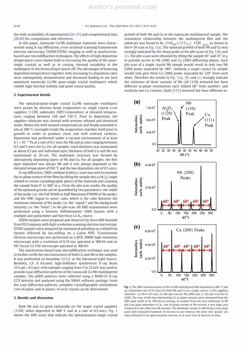
Both Nb and Cu grow epitaxially on the single crystal sapphire(112̄0) when deposited at 400 °C and at a rate of 0.5 nm/s. Fig. 1shows the XRD scans that indicate the epitaxial/quasi-single crystal
growth of both Nb and Cu in the nanoscale multilayered sample. Theorientation relationship between the multilayered film and thesubstrate was found to be 110f gNbk 111f gCuk
�112
�0�Al2O3
as shown inthe θ–2θ scan in Fig. 1(a). The epitaxial growth of both Nb and Cu wasstrongly indicated by the sharp peaks in the phi-scans in Fig. 1(b) and(c). The phi-scans were obtained by tilting the sample 45° and 35° in χto provide access to Nb {200} and Cu {200} diffracting planes. Suchphi-scan of a single crystal Nb sample would result in only two Nb{200} peaks separated by 180°; similarly a single crystal Cu samplewould only give three Cu {200} peaks separated by 120° from eachother. Therefore the results in Fig. 1(a), (b) and (c) strongly indicatethe existence of three variants of Nb (all {110} textured but havedifferent in-plane orientations each shifted 60° from another) andsimilarly two Cu variants (both {111} textured but have different in-
Fig. 1. The XRD characterization of the Cu/Nb multilayered film deposited at 400 °C andat a deposition rate of 0.5 nm/s for both Nb and Cu on a single crystal (112 ̄0) sapphiresubstrate: (a) the θ–2θ scan, (b) the phi-scan for Nb {200} and (c) the phi-scan for Cu{200}. The sizes of the two intertwining Cu in-plane variants were estimated from theXRD peak width to be 100 nm on average. As evident from the non-uniformity in Nbphi-scan peak intensities in (b), one in-plane variant of Nb covered a very large areacompared to the other two Nb variants. The dominant variant is effectively a very largegrain with estimated hundreds of microns in size whereas the other two “grains” areonly estimated to be approximately microns or at most tens of microns in sizes.
4138 A.S. Budiman et al. / Thin Solid Films 519 (2011) 4137–4143
Author's personal copy
plane orientations each shifted 60° from the other) in each of therespective layers of the Cu/Nb multilayer sample.
In the Cu case, the two in-plane variants are likely to have Σ=3,{112} twinned boundary relationship with a rotation of 60°commonly found in FCC crystals with growth direction normal tothe close-packed planes. Such twin growth in Cu has been widelyreported especially in thin films on substrates [30,31]. Also suchepitaxial growth of twinned crystals related to each other by 60°rotation about the [111] axis in an FCC film on a single crystal sapphirehas been specifically reported by Ramanathan et al. [22] as well as inother similar studies [32–35]. They found that such films exhibit amicrostructure typical of the mazed bicrystal morphology, whichconsists of two intertwining orientation variants forming a maze-likestructure [22,32–35]. Further annealing experiments of such sampleswith hardly any noticeable change in the microstructure stronglyindicate that this mazed bicrystal structure forms a low-energyconfiguration for the FCC films on a single crystal sapphire [22]. Hence,it is reasonable to assume that such an energetically favorablestructure also forms in our sample.
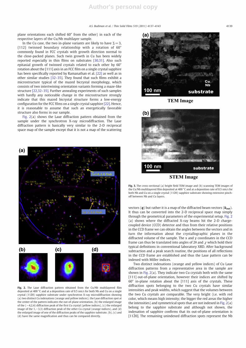
Fig. 2(a) shows the Laue diffraction pattern obtained from thesample under the synchrotron X-ray microdiffraction. The Lauediffraction pattern is basically very similar to the 2-D reciprocalspace map of the sample except that it is not a map of the scattering
vectors (q) but rather it is a map of the diffracted beam vectors (kout).It thus can be converted into the 2-D reciprocal space map simplythrough the geometrical parameters of the experimental setup. Fig. 2(a) shows where the diffracted X-ray beams hit the 2-D charge-coupled device (CCD) detector and thus from their relative positionsin the CCD frame we can obtain the angles between the vectors and inturn the information about the crystallographic planes in thediffracted volume of the sample. The x and y coordinates in the CCDframe can thus be translated into angles of 2θ and χ which hold theirtypical definitions in conventional laboratory XRD. After backgroundsubtraction and a peak search routine, the positions of all reflectionsin the CCD frame are established and thus the Laue pattern can beindexed with Miller indices.
Two distinct indexations (orange and yellow indices) of Cu Lauediffraction patterns from a representative area in the sample areshown in Fig. 2(a). They indicate two Cu crystals both with the same[111] out-of-plane orientation, however their indices are shifted by60° in-plane rotation about the [111] axis of the crystals. Thesediffraction spots belonging to the two Cu crystals have similarintensities and peak widths, which suggest that the volumes betweenthe two Cu crystals are comparable. The very bright (i.e. with redcolor, which means high intensity; the bigger the red areas the higherthe intensities) and symmetrical spots that are not indexed in Fig. 2(a)belong to the sapphire substrate and although not shown, theindexation of sapphire confirms that its out-of-plane orientation is[112̄0]. The remaining unindexed diffraction spots represent the Nb
Fig. 2. The Laue diffraction pattern obtained from the Cu/Nb multilayered filmdeposited at 400 °C and at a deposition rate of 0.5 nm/s for both Nb and Cu on a singlecrystal (112 ̄0) sapphire substrate under synchrotron X-ray microdiffraction showing(a) two distinct Cu indexations (orange and yellow indices); the Laue diffraction spot atthe center of the pattern indicates the out-of-plane orientation, (b) the enlarged imageof the (−4,2,4) diffraction peak of the first Cu crystal (yellow indices), (c) the enlargedimage of the 1,−3,3) diffraction peak of the other Cu crystal (orange indices), and (d)the enlarged image of one of the diffraction peaks of the sapphire substrate. (b), (c) and(d) have the same magnification and thus can be compared directly.
Fig. 3. The cross-sectional (a) bright field TEM image and (b) scanning TEM images ofthe Cu/Nb multilayered film deposited at 400 °C and at a deposition rate of 0.5 nm/s forboth Nb and Cu on a single crystal (112 ̄0) sapphire substrate showing extensive pinch-off between Nb and Cu layers.
4139A.S. Budiman et al. / Thin Solid Films 519 (2011) 4137–4143
Author's personal copy
crystals and although again not shown in Fig. 2(a) they confirm theexistence of three Nb crystals all with the same {110} out-of-planeorientations each shifted by 60° in-plane rotation about their [110]axis from the others.
These observations with the synchrotron X-ray microdiffractionthus confirm the earlier laboratory XRD results and provide theevidence of the existence of the two Cu variants and the three Nbvariants in the epitaxial Cu/Nb films as earlier indicated by the phi-scans. They are also consistent with the possibility of the mazedbicrystal morphology in our sample, which consists of two intertwin-ing orientation variants forming amaze-like structure, as described byRamanathan et al. [22]. Fig. 2(b) shows the enlarged image of one ofthe Cu diffraction spots belonging to one of the Cu crystals whereasFig. 2(c) shows one Cu diffraction spot belonging to the other Cucrystal in the sample. It shows a rather diffuse diffraction peak(compare that with Fig. 2(d) which shows the enlarged image of oneof the sapphire diffraction spots) but still easily recognizable by thepeak search routine and thus the crystal indexation can still be donewith considerably high confidence. The broad diffraction peak isconsistent with the rather small size of the individual Cu crystals (theindividual layer thickness of each layer of Cu is only 20 nm).
The XRD characterization results (both the laboratory andsynchrotron-based) thus so far show the high quality epitaxial/quasi-single crystals of Nb and Cu. However Fig. 3 suggests that this isnot yet the complete picture. Fig. 3(a) and (b) shows the XTEM imagesof the Cu–Nbmultilayered film on the sapphire substrate. They clearlyshow areas of layer pinch-off due to diffusion along groovingcolumnar grain boundaries during elevated temperature deposition.
The observation of layer pinch-off at high temperatures motivatedus to deposit the film at lower temperatures and at much higherdeposition rates especially for Cu layers to minimize the occurrence ofthe pinch-off events by lowering the thermal energy and minimizingthe time available for Cu atoms to diffuse. However as can beexpected, lower temperatures would also reduce the quality of theepitaxial/quasi-single crystal films and at sufficiently low tempera-tures, ultimately result in growth of polycrystalline films. Clearlydeposition parameters must be optimized in order to grow highquality epitaxial/quasi-single crystal multilayers with continuouslayers of Cu and Nb.
Therefore there really are two figures of merit in the present study.First, the quality of the epitaxial/quasi-single crystal nanolayered film
and second, the extent of layer continuity (i.e. thermal stability) in themultilayer materials. We then performed full characterization of bothfigures of merit over a range of deposition temperatures and Cudeposition rates (for reasons already mentioned above Nb depositionrates were fixed at 0.5 nm/s). The quality of the epitaxial/quasi-singlecrystal films can be quantified in terms of the FWHM and the SNR inthe phi-scans. The results of the characterization of the quality of theepitaxial/quasi-single crystal films over deposition temperaturesranging from 150 to 750 °C and Cu deposition rates ranging from0.5 to 5 nm/s are shown in Table 1. As a reminder in all these samples,the first layer of Nb (the “seed” layer) was always deposited at a hightemperature of 950 °C and at a low deposition rate of 0.5 nm/s.
Table 1The quality of the epitaxial/quasi-single crystal growth with respect to depositiontemperatures ranging from 150 to 750 °C. The instrumental broadening as estimatedfrom the FWHM of diffraction peaks of the single crystal sapphire substrate wasdetermined to be 0.09°. For both FWHM and SNR, the average of the 6 peaks observed ineach of the phi-scans was given. The standard deviations for FWHM data in this tableare less than 2%, whereas for the SNR data, the standard deviation differs considerablybetween that of Cu {200} and Nb {200} phi-scan peaks. The standard deviations for SNRdata for Nb and Cu in this table are not more than 31% and 5% respectively as evident forinstance from the non-uniformity in the Nb phi-scan peak intensities and theconsiderably more uniform Cu phi-scan peak intensities in Figs. 1 and 5.
Depositiontemperatures
Cu deposition rates
0.5 nm/s 2.5 nm/s 5 nm/s
FWHM (°) SNR FWHM (°) SNR FWHM (°) SNR
750 °C Cu 0.6 1663 0.5 596 0.5 588Nb 0.8 521 0.9 292 0.8 1012
600 °C Cu 0.9 1226 0.9 886 0.8 488Nb 1.1 489 1.2 327 1.1 224
400 °C Cu 1.6 309 1.7 256 1.4 226Nb 1.5 131 1.7 122 1.7 54
250 °C Cu 1.3 211 1.3 112 2.2 179Nb 1.5 106 1.6 89 3.6 124
200 °C Cu 3.4 128Nb 4.6 122
150 °C Cu 5.2 116Nb 5.8 68
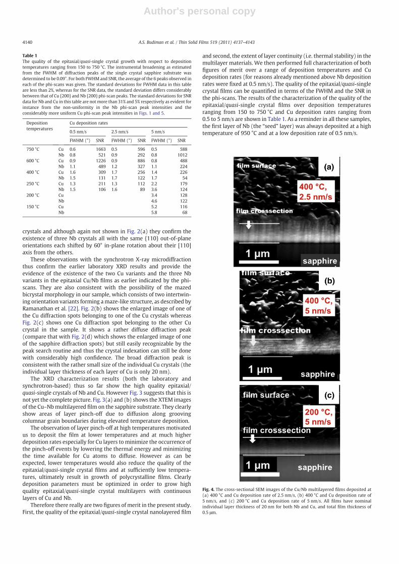
Fig. 4. The cross-sectional SEM images of the Cu/Nb multilayered films deposited at(a) 400 °C and Cu deposition rate of 2.5 nm/s, (b) 400 °C and Cu deposition rate of5 nm/s, and (c) 200 °C and Cu deposition rate of 5 nm/s. All films have nominalindividual layer thickness of 20 nm for both Nb and Cu, and total film thickness of0.5 μm.
4140 A.S. Budiman et al. / Thin Solid Films 519 (2011) 4137–4143
Author's personal copy
It must be noted that similar microstructures (i.e. epitaxial/quasi-single crystal films of Nb and Cu with the same orientationrelationship) as described above for the sample that was depositedat 400 °C and Cu deposition rate of 0.5 nm/s were maintained acrossthe ranges of deposition temperatures and Cu deposition rates.Table 1 clearly shows that the quality of the epitaxial/quasi-singlecrystal layers of both Nb and Cu increases with increasing tempera-tures and to the second order it decreases with increasing Cudeposition rates. Evidently, epitaxial growth requires thermal energyand ample time to grow in a well ordered manner. When Cudeposition rate is increased, there is less time for Cu to grow wellaligned crystals and higher probability of generating defects in the
crystals. Such defects and disordered growth of the Cu layers promotesimilar defects and disordered growth in the subsequent layers of Nb.
The results of the characterization of the extent of layerdiscontinuities (due to the pinch-off events) over depositiontemperatures ranging from 150 to 750 °C and Cu deposition ratesranging from 0.5 to 5 nm/s are shown in a few representative XSEMimages in Fig. 4. The effect of increasing Cu deposition rate is clearlyshown in the comparison between Fig. 4(a) and (b). Here bothsamples were deposited at otherwise the same deposition para-meters, except for the Cu deposition rate. Fig. 4(b) representing asample deposited at a higher Cu deposition rate of 5 nm/s clearlyshows a film cross-section with much higher extent of layercontinuities than that of Fig. 4(a) which represents a sampledeposited at a lower Cu deposition rate of 2.5 nm/s. This confirmsour earlier hypothesis that higher deposition rate of Cu would restrictthe time available for Cu atoms to diffuse around to the adjacent layersof Nb resulting in significantly fewer pinch-off events and leading tomuch higher extent of layer continuities. The effects of increasing Cudeposition rate can be further confirmed by comparing Fig. 4(a) and(b) with Fig. 3(a) and (b) which represents a sample deposited at aneven lower Cu deposition rate of 0.5 nm/s although direct comparisonmight be difficult as Fig. 3(a) and (b) was taken at a much highermagnification. Nevertheless they show a much higher level of pinch-off and much less resemblance of layer continuities especially if seenat much lower magnifications.
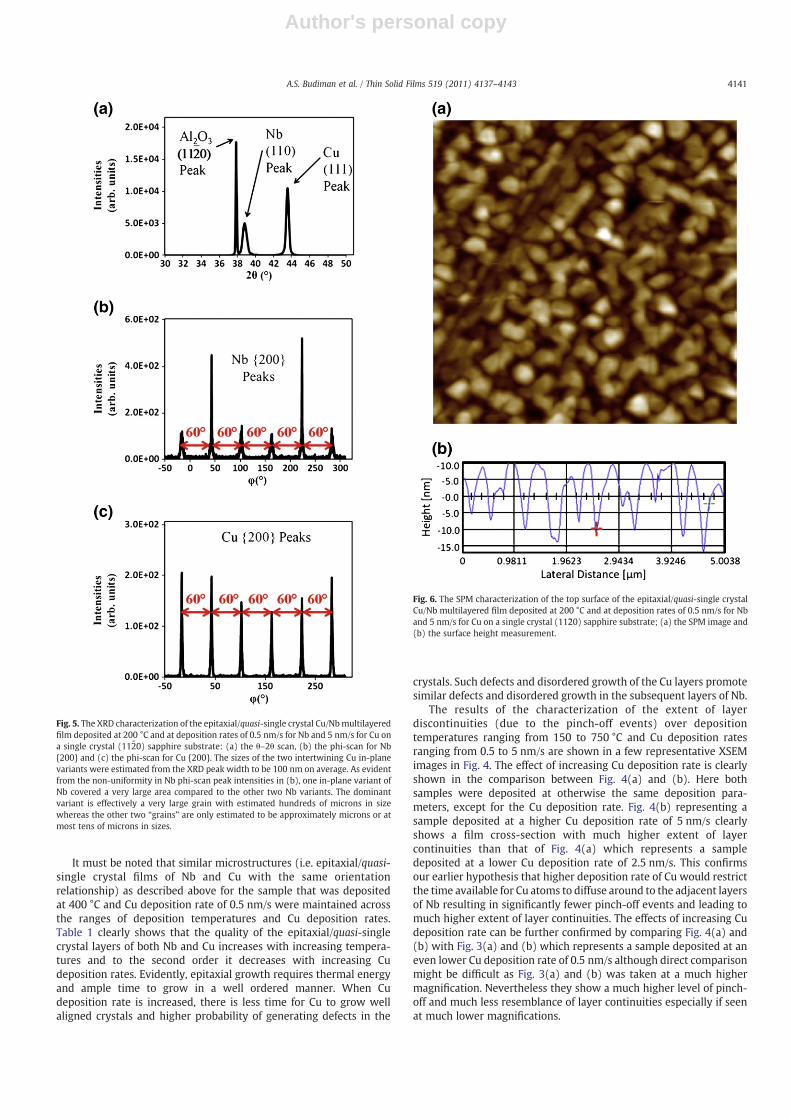
Fig. 5. The XRD characterization of the epitaxial/quasi-single crystal Cu/Nbmultilayeredfilm deposited at 200 °C and at deposition rates of 0.5 nm/s for Nb and 5 nm/s for Cu ona single crystal (112 ̄0) sapphire substrate: (a) the θ–2θ scan, (b) the phi-scan for Nb{200} and (c) the phi-scan for Cu {200}. The sizes of the two intertwining Cu in-planevariants were estimated from the XRD peak width to be 100 nm on average. As evidentfrom the non-uniformity in Nb phi-scan peak intensities in (b), one in-plane variant ofNb covered a very large area compared to the other two Nb variants. The dominantvariant is effectively a very large grain with estimated hundreds of microns in sizewhereas the other two “grains” are only estimated to be approximately microns or atmost tens of microns in sizes.
Fig. 6. The SPM characterization of the top surface of the epitaxial/quasi-single crystalCu/Nb multilayered film deposited at 200 °C and at deposition rates of 0.5 nm/s for Nband 5 nm/s for Cu on a single crystal (112 ̄0) sapphire substrate; (a) the SPM image and(b) the surface height measurement.
4141A.S. Budiman et al. / Thin Solid Films 519 (2011) 4137–4143
Author's personal copy
The effect of lowering the deposition temperature is clearly shownin the comparison between Fig. 4(b) that we have seen earlier andFig. 4(c). Here both samples were deposited at otherwise the samedeposition parameters, except for the temperature. Fig. 4(c) repre-senting a sample deposited at a lower deposition temperature of200 °C clearly shows a film cross-section with much higher extent oflayer continuities than that of Fig. 4(b) which represents a sampledeposited at a temperature of 400 °C. This again confirms our earlierhypothesis that lower deposition temperature would restrict thethermal energy needed for Cu atoms to diffuse around to the adjacentlayers of Nb resulting in significantly fewer pinch-off events andleading to much higher extent of layer continuities.
Herein therefore lies our need to optimize the depositionparameters in order to achieve our objective of a high quality andthermally stable epitaxial/quasi-single crystal multilayer sample.Increasing temperatures increases the quality of the epitaxial/quasi-single crystal films but decreases the thermal stability of the layers asshown in Fig. 3(a) and (b). However lowering the temperature toomuch would result in a polycrystalline growth like it does in roomtemperature. Increasing Cu deposition rate increases the thermalstability of the layers significantly but reduces the quality of theepitaxial/quasi-single crystal growth although slightly. In the end, weconsider the sample shown in Fig. 4(c) to be our best optimizednanoscale Cu/Nb epitaxial/quasi-single crystal multilayers. It wasdeposited at a temperature of 200 °C and at a rate of 0.5 nm/s for Nband a much higher rate of 5 nm/s for Cu. It exhibits both layers of Cuand Nb that are largely continuous with just a minimum amount ofdiscontinuities due to the pinch-off events while maintaining thedesired microstructure with a still reasonably high quality of theepitaxial/quasi-single crystal growth.
Fig. 5 shows the complete XRD characterization of the sample. The θ–2θ scan of this sample as shown in Fig. 5(a) confirms the preferentialorientation, and thephi-scansof Cu {200}andNb {200} as shown in Fig. 5(b) and (c) respectively also confirm the in-plane alignment of Cu andNb. The still reasonably high quality of the epitaxial/quasi-single crystalgrowth of Cu andNb is also evident from the FWHM and the SNR for thesample deposited at 200 °C and at a Cu deposition rate of 5 nm/s asshown in Table 1. Fig. 4(c) shows also the top surface in addition to thecross-section of the 0.5 μm-thick multilayer film. The top surfaceindicates that it is rather rough and confirmed by the scanning probemicroscopy (SPM) image as shown in Fig. 6(a) as well as by the surfaceheight measurement as shown in Fig. 6(b). The surface roughnessincreases with increasing temperatures.
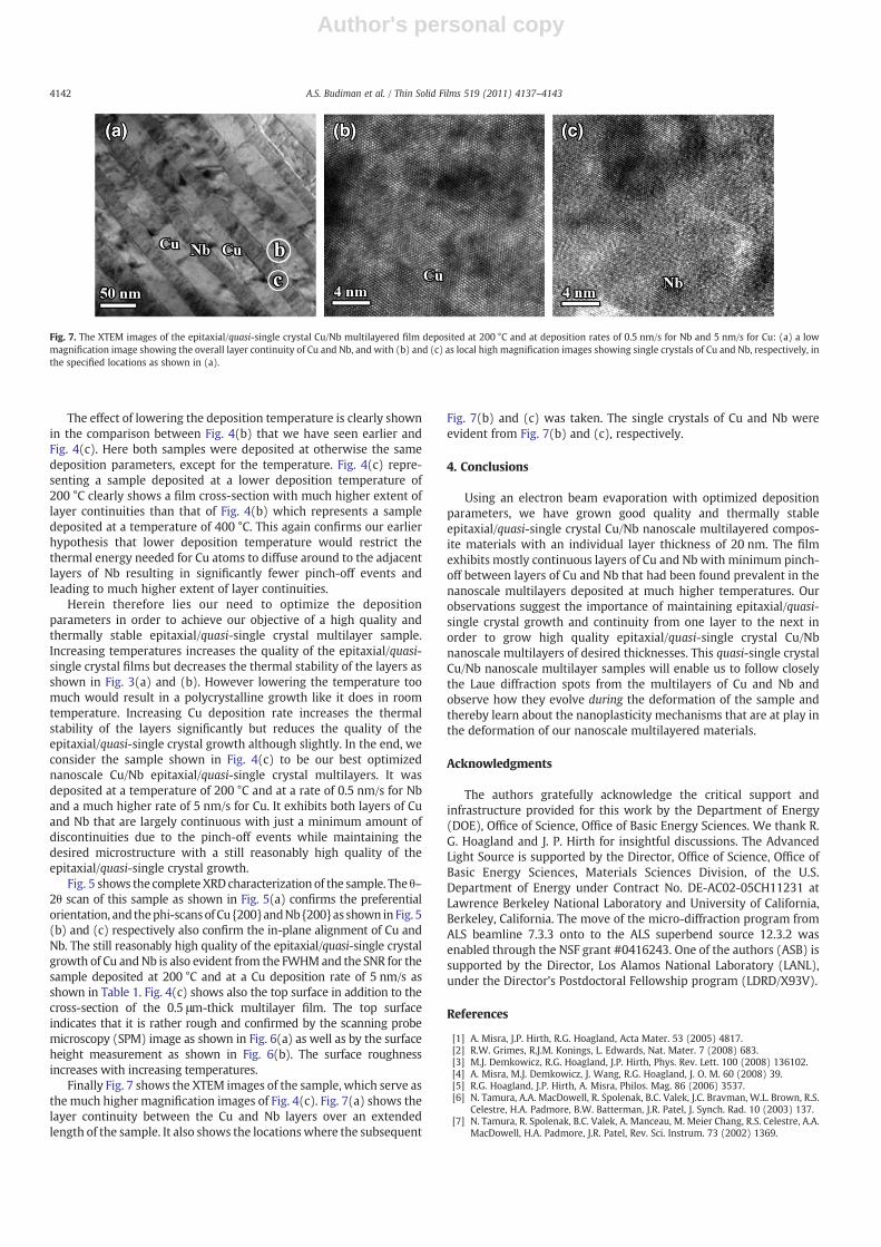
Finally Fig. 7 shows the XTEM images of the sample, which serve asthe much higher magnification images of Fig. 4(c). Fig. 7(a) shows thelayer continuity between the Cu and Nb layers over an extendedlength of the sample. It also shows the locationswhere the subsequent
Fig. 7(b) and (c) was taken. The single crystals of Cu and Nb wereevident from Fig. 7(b) and (c), respectively.
4. Conclusions
Using an electron beam evaporation with optimized depositionparameters, we have grown good quality and thermally stableepitaxial/quasi-single crystal Cu/Nb nanoscale multilayered compos-ite materials with an individual layer thickness of 20 nm. The filmexhibits mostly continuous layers of Cu and Nb with minimum pinch-off between layers of Cu and Nb that had been found prevalent in thenanoscale multilayers deposited at much higher temperatures. Ourobservations suggest the importance of maintaining epitaxial/quasi-single crystal growth and continuity from one layer to the next inorder to grow high quality epitaxial/quasi-single crystal Cu/Nbnanoscale multilayers of desired thicknesses. This quasi-single crystalCu/Nb nanoscale multilayer samples will enable us to follow closelythe Laue diffraction spots from the multilayers of Cu and Nb andobserve how they evolve during the deformation of the sample andthereby learn about the nanoplasticity mechanisms that are at play inthe deformation of our nanoscale multilayered materials.
Acknowledgments
The authors gratefully acknowledge the critical support andinfrastructure provided for this work by the Department of Energy(DOE), Office of Science, Office of Basic Energy Sciences. We thank R.G. Hoagland and J. P. Hirth for insightful discussions. The AdvancedLight Source is supported by the Director, Office of Science, Office ofBasic Energy Sciences, Materials Sciences Division, of the U.S.Department of Energy under Contract No. DE-AC02-05CH11231 atLawrence Berkeley National Laboratory and University of California,Berkeley, California. The move of the micro-diffraction program fromALS beamline 7.3.3 onto to the ALS superbend source 12.3.2 wasenabled through the NSF grant #0416243. One of the authors (ASB) issupported by the Director, Los Alamos National Laboratory (LANL),under the Director's Postdoctoral Fellowship program (LDRD/X93V).
References
[1] A. Misra, J.P. Hirth, R.G. Hoagland, Acta Mater. 53 (2005) 4817.[2] R.W. Grimes, R.J.M. Konings, L. Edwards, Nat. Mater. 7 (2008) 683.[3] M.J. Demkowicz, R.G. Hoagland, J.P. Hirth, Phys. Rev. Lett. 100 (2008) 136102.[4] A. Misra, M.J. Demkowicz, J. Wang, R.G. Hoagland, J. O. M. 60 (2008) 39.[5] R.G. Hoagland, J.P. Hirth, A. Misra, Philos. Mag. 86 (2006) 3537.[6] N. Tamura, A.A. MacDowell, R. Spolenak, B.C. Valek, J.C. Bravman, W.L. Brown, R.S.
Celestre, H.A. Padmore, B.W. Batterman, J.R. Patel, J. Synch. Rad. 10 (2003) 137.[7] N. Tamura, R. Spolenak, B.C. Valek, A. Manceau, M. Meier Chang, R.S. Celestre, A.A.
MacDowell, H.A. Padmore, J.R. Patel, Rev. Sci. Instrum. 73 (2002) 1369.
Fig. 7. The XTEM images of the epitaxial/quasi-single crystal Cu/Nb multilayered film deposited at 200 °C and at deposition rates of 0.5 nm/s for Nb and 5 nm/s for Cu: (a) a lowmagnification image showing the overall layer continuity of Cu and Nb, and with (b) and (c) as local high magnification images showing single crystals of Cu and Nb, respectively, inthe specified locations as shown in (a).
4142 A.S. Budiman et al. / Thin Solid Films 519 (2011) 4137–4143
Author's personal copy
[8] M. Kunz, N. Tamura, K. Chen, A.A. MacDowell, R.S. Celestre, M.M. Church, S. Fakra,E.E. Domning, J.M. Glossinger, J.L. Kirschman, G.Y. Morrison, D.W. Plate, B.V. Smith,T. Warwick, V.V. Yashchuk, H.A. Padmore, E. Ustundag, Rev. Sci. Instrum. 80(2009) 035108.
[9] A.S. Budiman, S.M. Han, J.R. Greer, N. Tamura, J.R. Patel, W.D. Nix, Acta Mater. 56(2008) 602.
[10] G. Feng, A.S. Budiman, W.D. Nix, N. Tamura, J.R. Patel, J. Appl. Phys. 104 (2008)043501.
[11] G. Lee, J.Y. Kim, A.S. Budiman, N. Tamura, M. Kunz, K. Chen, M.J. Burek, J.R. Greer, T.Y. Tsui, Acta Mater. 58 (2010) 1361.
[12] A.S. Budiman, W.D. Nix, N. Tamura, B.C. Valek, K. Gadre, J. Maiz, R. Spolenak, J.R.Patel, Appl. Phys. Lett. 88 (2006) 233515.
[13] A.S. Budiman, P. Besser, C.S. Hau-Riege, A. Marathe, Y.C. Joo, N. Tamura, J.R. Patel,W.D. Nix, J. Electron. Mater. 38 (2009) 379.
[14] A.S. Budiman, C.S. Hau-Riege, W.C. Baek, C. Lor, A. Huang, H.S. Kim, G. Neubauer, J.Pak, P. Besser, W.D. Nix, J. Electron. Mater. 39 (2010) 2483.
[15] J.Wang, N. Li, O. Anderoglu, X. Zhang, A. Misra, J.Y. Huang, J.P. Hirth, ActaMater. 58(2010) 2262.
[16] J. Ye, R.K. Mishra, A.M. Minor, Scr. Mater. 59 (2008) 951.[17] J. Birch, Y. Yamamoto, L. Hultman, G. Radnoczi, J.E. Sundgren, Vacuum 41 (1990)
1231.[18] C. Engstrom, A. Madan, J. Birch, M. Nastasi, L. Hultman, S.A. Barnett, J. Mater. Res.
15 (2000) 554.
[19] G.R. English, G.F. Simenson, B.M. Clemens, W.D. Nix, Mater. Res. Symp. Proc. 356(1995) 363.
[20] S.Yamamoto,H.Naramoto,B. Tuchiya,K.Narumi,Y.Aoki, ThinSolidFilms335(1998)85.[21] O. Igarashi, Jpn. J. Appl. Phys. 34 (1995) 563.[22] S. Ramanathan, B.M. Clemens, P.C. McIntyre, Philos. Mag. 81 (2001) 2073.[23] R. Loloee, M.A. Crimp, W. Zhu, W.P. Pratt, Mater. Res. Symp. Proc. 528 (1998) 203.[24] N. Mara, D. Bhattacharryya, P. Dickerson, R.G. Hoagland, A. Misra, Appl. Phys. Lett.
92 (2008) 231901.[25] A. Misra, R.G. Hoagland, J. Mater. Sci. 42 (2007) 1765.[26] K. Nyilas, A. Misra, T. Ungar, Acta Mater. 54 (2006) 751.[27] C.C. Aydiner, D.W. Brown, N. Mara, J. Almer, A. Misra, Appl. Phys. Lett. 94 (2009)
031906.[28] J. Wang, R.G. Hoagland, J.P. Hirth, A. Misra, Acta Mater. 56 (2008) 3109.[29] J. Wang, R.G. Hoagland, A. Misra, Scr. Mater. 60 (2008) 1067.[30] C. Lingk, M.E. Gross, W.L. Brown, J. Appl. Phys. 87 (2000) 2232.[31] O. Anderoglu, A. Misra, H. Wang, F. Ronning, M.F. Hundley, X. Zhang, Appl. Phys.
Lett. 93 (2008) 083108.[32] R.F.C. Farrow, G.R. Harp, R.F. Marks, T.A. Rabedeau, M.F. Toney, D. Weller, S.S.P.
Parkin, J. Cryst. Growth 133 (1993) 47.[33] M.L. Hildner, T.J. Minvielle, R.J. Wilson, Surf. Sci. 396 (1998) 16.[34] J.H. Song, W.K. Choi, K.H. Kim, J.C. Lee, S.C. Kim, H.B. Kim, M.H. Lee, K. Jeong, C.N.
Whang, Nucl. Instrum. Meth. B149 (1999) 361.[35] R. Vargas, T. Goto, W. Zhang, T. Hirai, Appl. Phys. Lett. 65 (1994) 1094.
4143A.S. Budiman et al. / Thin Solid Films 519 (2011) 4137–4143
Related Documents