TEA1999TK/2 GreenChip synchronous rectifier controller Rev. 3 — 13 September 2018 Product data sheet 1 General description The TEA1999TK is a member of a new generation of Synchronous Rectifier (SR) controller ICs for switched mode power supplies with adaptive gate drive for maximum efficiency at any load. The TEA1999TK is a dedicated controller IC for synchronous rectification on the secondary side of flyback converters. It incorporates the sensing stage and driver stage for driving the SR MOSFET, which is rectifying the output of the secondary transformer winding. The TEA1999TK can generate its own supply voltage for battery charging applications with low output voltage or for applications with high-side rectification. The TEA1999TK is fabricated in a Silicon-On-Insulator (SOI) process. 2 Features and benefits 2.1 Efficiency features • Adaptive gate drive for maximum efficiency at any load • Typical supply current in no-load operation below 250 μA 2.2 Application features • Operates in an output voltage range between 26 V and 0 V • Drain sense pin capable of handling input voltages up to 120 V • Self-supplying for operation with low output voltage • Self-supplying for high-side rectification without the use of an auxiliary winding • Operates with standard and logic level SR MOSFETs • Supports USB BC, QuickCharge, and smart charging applications • HVSON8 package 2.3 Control features • Adaptive gate drive for fast turn-off at the end of conduction • UnderVoltage LockOut (UVLO) with active gate pull-down • Blanking input for low and high switching frequency • Enable input for CCM operation and for disabling at start-up or shorted output

Welcome message from author
This document is posted to help you gain knowledge. Please leave a comment to let me know what you think about it! Share it to your friends and learn new things together.
Transcript
TEA1999TK/2GreenChip synchronous rectifier controllerRev. 3 — 13 September 2018 Product data sheet
1 General description
The TEA1999TK is a member of a new generation of Synchronous Rectifier (SR)controller ICs for switched mode power supplies with adaptive gate drive for maximumefficiency at any load.
The TEA1999TK is a dedicated controller IC for synchronous rectification on thesecondary side of flyback converters. It incorporates the sensing stage and driver stagefor driving the SR MOSFET, which is rectifying the output of the secondary transformerwinding.
The TEA1999TK can generate its own supply voltage for battery charging applicationswith low output voltage or for applications with high-side rectification.
The TEA1999TK is fabricated in a Silicon-On-Insulator (SOI) process.
2 Features and benefits
2.1 Efficiency features
• Adaptive gate drive for maximum efficiency at any load• Typical supply current in no-load operation below 250 μA
2.2 Application features
• Operates in an output voltage range between 26 V and 0 V• Drain sense pin capable of handling input voltages up to 120 V• Self-supplying for operation with low output voltage• Self-supplying for high-side rectification without the use of an auxiliary winding• Operates with standard and logic level SR MOSFETs• Supports USB BC, QuickCharge, and smart charging applications• HVSON8 package
2.3 Control features
• Adaptive gate drive for fast turn-off at the end of conduction• UnderVoltage LockOut (UVLO) with active gate pull-down• Blanking input for low and high switching frequency• Enable input for CCM operation and for disabling at start-up or shorted output
NXP Semiconductors TEA1999TK/2GreenChip synchronous rectifier controller
TEA1999TK All information provided in this document is subject to legal disclaimers. © NXP B.V. 2018. All rights reserved.
Product data sheet Rev. 3 — 13 September 20182 / 21
3 Applications
The TEA1999TK is intended for flyback power supplies. In such applications, it can drivethe external synchronous rectifier MOSFET, which replaces the diode for the rectificationof the voltage on the secondary winding of the transformer.
It can be used in all power supplies that require a high efficiency, like:
• Chargers• Adapters• Flyback power supplies with very low and/or variable output voltage
4 Ordering informationTable 1. Ordering information
PackageType number
Name Description Version
TEA1999TK/2 HVSON8 plastic thermal enhanced very thin small outline package; no leads; 8terminals; body 3 mm × 3 mm × 0.85 mm
SOT782-1
5 MarkingTable 2. Marking codeType number Marking code
TEA1999TK/2 E1999
NXP Semiconductors TEA1999TK/2GreenChip synchronous rectifier controller
TEA1999TK All information provided in this document is subject to legal disclaimers. © NXP B.V. 2018. All rights reserved.
Product data sheet Rev. 3 — 13 September 20183 / 21
6 Block diagram
V AND IREFERENCE
UNDERVOLTAGELOCKOUT
LOGIC
ENERGYSAVE
CONTROL
BLANKING
VOLTAGELIMITER
on regulation
CAP
XV
ENABLE
BLANKING
DRAIN
GATE
SOURCE
GND
aaa-024112
off regulation
turn-on
SWITCH-OFF
TURN-ON
OTP
+250 mV-20 mV-25 mV
---
TEA1999
Ich(CAP)
-400 mV
-
Figure 1. TEA1999TK block diagram

NXP Semiconductors TEA1999TK/2GreenChip synchronous rectifier controller
TEA1999TK All information provided in this document is subject to legal disclaimers. © NXP B.V. 2018. All rights reserved.
Product data sheet Rev. 3 — 13 September 20184 / 21
7 Pinning information
7.1 Pinning
aaa-026448
IC
CAP
ENABLE
XV
BLANKING
SOURCE GND
GATE DRAIN
Transparent top view
4 5
3 6
2 7
1 8
terminal 1index area
Figure 2. TEA1999TK pin configuration (SOT782-1)
7.2 Pin description
Table 3. Pin descriptionSymbol Pin Description
GATE 1 gate driver output for SR MOSFET
SOURCE 2 source sense input of SR MOSFET
ENABLE 3 enable input for SR operation
XV 4 external supply input
CAP 5 capacitor input for internal supply voltage
BLANKING 6 blanking input for minimum active time selection
GND 7 ground
DRAIN 8 drain sense input of SR MOSFET

NXP Semiconductors TEA1999TK/2GreenChip synchronous rectifier controller
TEA1999TK All information provided in this document is subject to legal disclaimers. © NXP B.V. 2018. All rights reserved.
Product data sheet Rev. 3 — 13 September 20185 / 21
8 Functional description
8.1 Introduction
The TEA1999TK is a controller IC for Synchronous Rectification (SR) in flybackapplications. It can drive the external synchronous rectifier MOSFET for the rectificationof the voltage on the secondary winding of the transformer. Figure 3 shows a typicalconfiguration.
DRIVER
PRIMARYCONTROLLER
SECONDARYCONTROLLER
S1
CAP
BLANKING
VCC
OPTO
GND
GATE
DRAINXV
GND
SOURCE
TEA1999
ISENSE
AUX
VCC
HV
CTRL
GND
PROTECT
8
6
2
7
3
5
4
1
aaa-023940
SR low side
ENABLE
Figure 3. TEA1999TK configuration with low-side rectification
8.2 Start-up and UnderVoltage LockOut (UVLO; CAP and XV pins)
The capacitor on the CAP pin supplies the TEA1999TK. At a low CAP voltage (< 3.7 V),the capacitor is charged via the DRAIN pin with a limited start-up current of typically15 mA. When the CAP voltage exceeds 3.7 V, the DRAIN pin or the XV pin can chargethe capacitor. When the XV voltage < 4.7 V, the capacitor is charged via the DRAIN pinwith a typical charge current of 125 mA. When the XV voltage ≥ 4.7 V, the capacitoris charged via the XV pin and an internal regulator. The regulator reduces the voltagedifference between the XV and CAP pins to a level below 100 mV.
When the voltage on the CAP pin exceeds Vstart(CAP) (3.7 V typical), the IC leaves theUVLO state and activates the synchronous rectifier circuitry. When the voltage dropsbelow 3.6 V (typical), the UVLO state is re-entered and the SR MOSFET gate driveroutput is actively kept low.
8.3 Drain sense (DRAIN pin)
The drain sense pin is an input pin capable of handling input voltages up to 120 V. Atpositive drain sense voltages, the gate driver is in off-mode with the gate driver pulleddown (pin GATE). At negative drain sense voltages, the IC enables the SynchronousRectification (SR) by sensing the drain source differential voltage.
NXP Semiconductors TEA1999TK/2GreenChip synchronous rectifier controller
TEA1999TK All information provided in this document is subject to legal disclaimers. © NXP B.V. 2018. All rights reserved.
Product data sheet Rev. 3 — 13 September 20186 / 21
8.4 Synchronous rectification (DRAIN and SOURCE pins)
The IC senses the voltage difference between the drain sense (DRAIN pin) and thesource sense (SOURCE pin) connections. This drain source differential voltage of the SRMOSFET is used to drive the gate of the SR MOSFET.
When this absolute voltage difference is higher than Vact(drv), the corresponding gatedriver output turns on the external SR MOSFET. When the external SR MOSFET isswitched on, the absolute voltage difference between the drain and the source senseconnections drops to below Vact(drv). The regulation phase follows the turn-on phase.
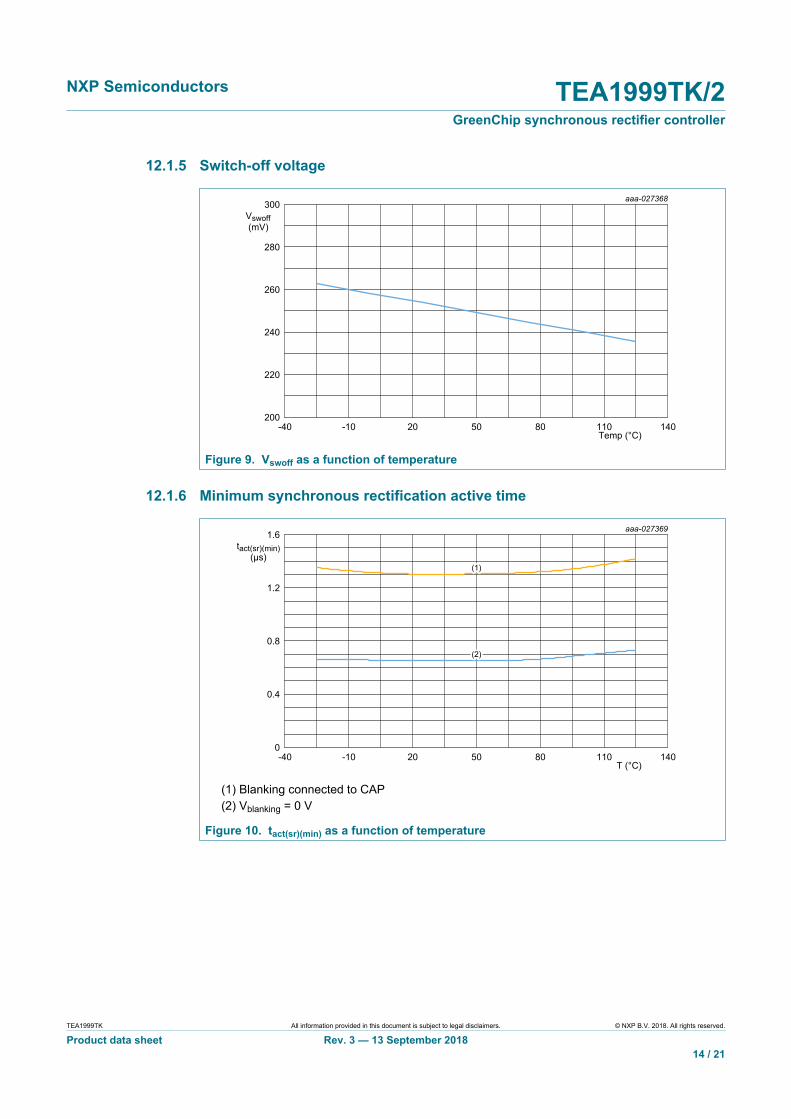
In the regulation phase, the IC regulates the difference between the drain and the sourcesense inputs to an absolute level of 25 mV. When the absolute difference exceeds 25 mV(Vreg(drv)), the gate driver output increases the gate voltage of the external SR MOSFETuntil the 25 mV level is reached. The SR MOSFET does not switch off at low current. Toavoid that the device switches off because of ringing, a minimum on-time of 1.5 μs (ttact(sr)(min)) is integrated.
When the absolute difference < 20 mV, the gate driver output decreases the gate voltageof the external SR MOSFET. The voltage waveform on the gate of the SR MOSFETfollows the waveform of the current through the SR MOSFET. When the current throughthe SR MOSFET reaches zero, the SR MOSFET is switched off quickly.
After SR MOSFET switch-off, the drain voltage increases. When the drain voltageexceeds 250 mV, a low ohmic gate pull-down of 3 Ω keeps the gate of the SR MOSFETswitched off.
8.5 Gate driver (GATE pin)
The gate driver circuit charges the gate of the external SR MOSFET during the risingpart of the current. The driver circuit discharges the gate during the falling part of thecurrent. The gate driver has a source capability of typically 0.70 A. It has a sink capabilityof typically 0.50 A. The source and sink capabilities allow fast turn-on and fast turn-off ofthe external SR MOSFET.
The maximum output voltage of the driver is limited to the voltage on the CAP pin. Themaximum output voltage ranges between 4.7 V and 10 V, depending on the voltage onthe CAP pin. The high output gate voltage drives all MOSFET brands to the minimum on-state resistance. In applications where the IC is supplied with 5 V, the maximum outputvoltage of the driver is 4.90 V, and logic level SR MOSFETs can be used.
The IC is self-supplying in applications with high-side rectification or in battery chargingapplications with an output voltage < 4.7 V. When the XV pin is connected to groundfor driving standard SR MOSFETs, the driver is regulated to 10 V. When the XV pinis connected to the converter output for driving logic-level SR MOSFETs, the driver isregulated to the voltage on the XV pin with a minimum of 4.7 V.

NXP Semiconductors TEA1999TK/2GreenChip synchronous rectifier controller
TEA1999TK All information provided in this document is subject to legal disclaimers. © NXP B.V. 2018. All rights reserved.
Product data sheet Rev. 3 — 13 September 20187 / 21
aaa-028212
0
VCAPVG(MAX)
5 VX V
10 V 26 V1 V
10 V
9 V
4.7 V
Figure 4. Maximum gate voltage (VG(max))
During start-up conditions (VCAP < Vstart(CAP)) and UVLO, the driver output voltage isactively pulled low.
When the XV voltage exceeds 10 V, the CAP voltage and VG(max) are limited to typically10.7 V. The XV voltage is allowed to increase until the 26 V limit is reached.
8.6 Source sense (SOURCE pin)
The IC is equipped with an additional source sense pin (SOURCE). This pin is used formeasuring the drain-to-source voltage of the external SR MOSFET. Voltage differenceson PCB tracks because of parasitic inductance in combination with large dI/dt values, cancause errors. To minimize these errors, the source sense input must be connected asclose as possible to the SOURCE pin of the external SR MOSFET.
8.7 Overtemperature protection (GATE pin)
Overtemperature protection is triggered when the output of the gate driver:
• Has a load that is too high• Is short-circuited to ground• Is short-circuited to the SOURCE pin
The OTP circuit is triggered at 165 °C. It actively pulls down the gate driver output. Whenthe temperature has decreased to 145 °C, the circuit resumes normal operation.
8.8 Enable input (ENABLE pin)
The enable input can be used for enabling and disabling the SR driver.
Disabling the SR driver can be desired during start-up or during a short-circuit of theoutput.
The enable input can be used for turning off the SR in CCM operation.
If the output voltage is higher than 2 V, input connect to the XV pin enables the SRoperation. Pulling the input to ground disables the driver.
An open input enables the SR operation by an internal 1 μA pull-up current.
NXP Semiconductors TEA1999TK/2GreenChip synchronous rectifier controller
TEA1999TK All information provided in this document is subject to legal disclaimers. © NXP B.V. 2018. All rights reserved.
Product data sheet Rev. 3 — 13 September 20188 / 21
8.9 Blanking input (BLANKING pin)
The blanking input can set the minimum active time (tact(sr)(min)).
An open pin or a pin connected to the CAP pin can be used for a long blanking time(1.5 μs) for applications with a switching frequency of up to 150 kHz.
A pin connected to ground can be used for a short blanking time (0.8 μs) for applicationswith a switching frequency of up to 300 kHz.

NXP Semiconductors TEA1999TK/2GreenChip synchronous rectifier controller
TEA1999TK All information provided in this document is subject to legal disclaimers. © NXP B.V. 2018. All rights reserved.
Product data sheet Rev. 3 — 13 September 20189 / 21
9 Limiting valuesTable 4. Limiting valuesIn accordance with the Absolute Maximum Rating System (IEC 60134). All voltages are measuredwith respect to ground (pin 2); positive currents flow into the chip. Voltage ratings are valid providedother ratings are not violated; current ratings are valid provided the other ranges are not violated.
Symbol Parameter Conditions Min Max Unit
Voltages
VXV voltage on pin XV −0.4 +26 V
Vsense(DRAIN) sense voltage on pin DRAIN −0.8 +120 V
Vsense(SOURCE) sense voltage on pinSOURCE
−0.4 +0.4 V
VENABLE voltage on pin ENABLE −0.4 +26 V
VBLANKING voltage on pin BLANKING −0.4 VCAP V
General
Ptot total power dissipation Tamb = 90 °C - 1 W
Tstg storage temperature −55 +150 °C
Tj junction temperature −40 +150 °C
ElectroStatic Discharge (ESD)
class 2
human bodymodel
[1] - 2000 V
charged devicemodel
- 500 V
VESD electrostatic dischargevoltage
machine model [2] - 200 V
[1] Equivalent to discharging a 100 pF capacitor through a 1.5 kΩ series resistor.[2] Equivalent to discharging a 200 pF capacitor through a 10 Ω series resistor and a 0.75 μH inductor.
10 Recommended operating conditionsTable 5. Recommended operating conditionsSymbol Parameter Conditions Min Typ Max Unit
VXV voltage on pin XV 0 - 21 V
VDRAIN voltage on pin DRAIN peak voltage inswitching application
8 - 120 V

NXP Semiconductors TEA1999TK/2GreenChip synchronous rectifier controller
TEA1999TK All information provided in this document is subject to legal disclaimers. © NXP B.V. 2018. All rights reserved.
Product data sheet Rev. 3 — 13 September 201810 / 21
11 Thermal characteristicsTable 6. Thermal characteristicsSymbol Parameter Conditions Typ Unit
Rth(j-a) thermal resistance fromjunction to ambient
JEDEC test board 57 K/W
Rth(j-c) thermal resistance fromjunction to case
JEDEC test board 48 K/W
12 CharacteristicsTable 7. Characteristics−25 °C < Tj < +125 °C; Vxv = 5 V; ENABLE connected to XV; BLANKING connected to CAP; CCAP = 1 μF; CGATE = 10 nF(capacitor between the GATE and the GND pins); all voltages are measured with respect to ground (pin 2); currents arepositive when flowing into the IC; unless otherwise specified.
Symbol Parameter Conditions Min Typ Max Unit
Supply voltage management (XV and CAP pins)
Vstart(CAP) start voltage on pin CAP VXV = 0 V 3.5 3.7 3.9 V
Vstop(CAP) stop voltage on pin CAP VXV = 0 V 3.4 3.6 3.8 V
Istart(CAP) start current on pin CAP VXV = 5 V; VCAP = 0 V;VDRAIN = 12 V
−24 −15 −8 mA
power save operation
VXV = 0 V; VCAP = 8 V;VDRAIN = 12 V; Tj = 25 °C
−120 −80 −50 mA
Ich(CAP) charge current on pin CAP
VXV = 2 V; VCAP = 4 V;VDRAIN = 12 V; Tj = 25 °C
−160 −110 −50 mA
VXV = 0 V; VDRAIN = 15 V 9.0 9.4 9.8 V
VXV = 2 V; VDRAIN = 12 V 4.5 4.6 4.8 V
VXV = 5 V 4.8 4.9 5.0 V
VXV = 10 V 9.8 9.9 10.0 V
VI(CAP) input voltage on pin CAP
VXV = 26 V 10.3 10.7 11.1 V
power save operation;VDRAIN = 5.5 V; Tj = 25 °C
200 240 280 μAII(XV) input current on pin XV
normal operation; without gatecharge; VDRAIN step from 5.5 Vto −250 mV; Tj = 25 °C
1.0 1.2 1.4 mA
tact(pwrsave) power-save activation time 70 100 130 μs
Synchronous rectification sense input (DRAIN and SOURCE pins)
Vact(drv) driver activation voltage VSOURCE = 0 V; Tj = 25 °C −510 −470 −430 mV
Vreg(drv) driver regulation voltage VSOURCE = 0 V; Tj = 25 °C −30 −25 −20 mV
Vswoff switch-off voltage VSOURCE = 0 V 180 250 320 mV

NXP Semiconductors TEA1999TK/2GreenChip synchronous rectifier controller
TEA1999TK All information provided in this document is subject to legal disclaimers. © NXP B.V. 2018. All rights reserved.
Product data sheet Rev. 3 — 13 September 201811 / 21
Symbol Parameter Conditions Min Typ Max Unit
td(act)(drv) driver activation delay time VSOURCE = 0 V; normaloperation; time for step-onVDRAIN (2 V to −0.5 V) to risingof VG at 10 % of end value
- 40 - ns
td(deact)(drv) driver deactivation delay time VSOURCE = 0 V; normaloperation; time for step-onVDRAIN (−50 mV to 2 V) tofalling of VG at 90 % of beginvalue
- 40 - ns
VSOURCE = 0 V; normaloperation; time for step-onVDRAIN (−700 mV to +100 mV)to falling of VG at 90 % of beginvalue; without gate charge
1.1 1.4 1.8 μstact(sr)(min) minimum synchronousrectification active time
VSOURCE = 0 V; normaloperation; time for step-onVDRAIN (−700 mV to +100 mV)to falling of VG at 90 % of beginvalue; without gate charge;VBLANKING = 0 V
0.5 0.7 0.9 μs
Gate driver (GATE pin)
Isource source current peak.current; VXV = 5 V;Vds = −0.5 V; VG = 0 V
- -0.70 - A
regulation current; VXV = 5 V;Vds = 0 V; VG = 3 V
- 100 - mAIsink sink current
peak current; VXV = 5 V;Vds = 0.5 V; VG = 4 V
- 0.50 - A
Rpd(G) gate pull-down resistance VDRAIN = 0.5 V; IG = 100 mA;VXV = 5 V; Tj = 25 °C
2.6 3.2 4.0 Ω
VXV = 0 V 9.0 9.4 9.8 V
VXV = 2 V 4.45 4.60 4.75 V
VXV = 5 V 4.8 4.9 5.0 V
VXV = 10 V 9.8 9.9 10.0 V
VG(max) maximum gate voltage
VXV = 26 V 10.3 10.7 11.1 V
Enable function (ENABLE pin)
Vth(en) enable threshold voltage 1.1 1.6 2.0 V
Vth(dis) disable threshold voltage 1.0 1.5 1.9 V
td(en) enable delay time turn-on delay - 85 - ns
td(dis) disable delay time turn-off delay - 100 - ns
Temperature protection
Totp(act) activation overtemperatureprotection temperature
155 165 175 °C
Totp(hys) overtemperature protection triphysteresis
- 20 - °C

NXP Semiconductors TEA1999TK/2GreenChip synchronous rectifier controller
TEA1999TK All information provided in this document is subject to legal disclaimers. © NXP B.V. 2018. All rights reserved.
Product data sheet Rev. 3 — 13 September 201812 / 21
12.1 Temperature curves
12.1.1 Charge current (CAP pin)
aaa-027364
-40 -10 20 50 80 110 140-150
-120
-90
-60
-30
0
T (°C)
Ich(CAP)Ich(CAP)(mA)(mA)
(1)(1)
(2)(2)
(1) Ich(CAP) at VCAP = 8 V; VXV = 0 V(2) Ich(CAP) at VCAP = 4 V; VXV = 2 V
Figure 5. Ich(CAP) as a function of temperature
12.1.2 Operating current (XV pin)
aaa-027365
-40 -10 20 50 80 110 1400
400
800
1200
1600
T (°C)
II(XV)II(XV)(µA)(µA)
(2)(2)
(1)(1)
(1) II(XV) - normal operation(2) II(XV) - power save operation
Figure 6. II(XV) as a function of temperature

NXP Semiconductors TEA1999TK/2GreenChip synchronous rectifier controller
TEA1999TK All information provided in this document is subject to legal disclaimers. © NXP B.V. 2018. All rights reserved.
Product data sheet Rev. 3 — 13 September 201813 / 21
12.1.3 Driver regulation voltage
aaa-027366
-40 -10 20 50 80 110 140-30
-25
-20
-15
-10
-5
0
T (°C)
Vreg(drv)Vreg(drv)(mV)(mV)
Figure 7. Vreg(drv) as a function of temperature
12.1.4 Gate pull-down resistance
aaa-027367
-40 -10 20 50 80 110 1400
1
2
3
4
5
T (°C)
Rpd(G)Rpd(G)(Ω)(Ω)
Figure 8. Rpd(G) as a function of temperature
NXP Semiconductors TEA1999TK/2GreenChip synchronous rectifier controller
TEA1999TK All information provided in this document is subject to legal disclaimers. © NXP B.V. 2018. All rights reserved.
Product data sheet Rev. 3 — 13 September 201814 / 21
12.1.5 Switch-off voltage
aaa-027368
-40 -10 20 50 80 110 140200
220
240
260
280
300
Temp (°C)
VswoffVswoff(mV)(mV)
Figure 9. Vswoff as a function of temperature
12.1.6 Minimum synchronous rectification active time
aaa-027369
-40 -10 20 50 80 110 1400
0.4
0.8
1.2
1.6
T (°C)
tact(sr)(min)tact(sr)(min)(μs)(μs)
(1)(1)
(2)(2)
(1) Blanking connected to CAP(2) Vblanking = 0 V
Figure 10. tact(sr)(min) as a function of temperature

NXP Semiconductors TEA1999TK/2GreenChip synchronous rectifier controller
TEA1999TK All information provided in this document is subject to legal disclaimers. © NXP B.V. 2018. All rights reserved.
Product data sheet Rev. 3 — 13 September 201815 / 21
13 Application information
A flyback switched mode power supply with the TEA1999TK consists of a primaryside controller with a primary switch, a transformer, and an output stage. To obtainlow conduction loss rectification, an SR MOSFET is used in the output stage. TheSR MOSFET can be placed low-side (see Figure 3) or can be placed high-side (seeFigure 11). In the high-side application, the TEA1999TK is self-supplying. The capacitoron the CAP pin supplies the TEA1999TK. When the drain voltage is positive, it is chargedvia the DRAIN pin.
The gate drive voltage for the synchronous rectifier switch is derived from the voltagedifference between the corresponding drain sense and source sense pins.
Special attention must be paid to the connection of the drain sense and source sensepins. The voltages measured on these pins are used for the gate drive voltage. Wrongmeasurement results in a less efficient gate drive because a gate voltage that is eithertoo low or too high. The connections to these pins must not interfere with the powerwiring.
The power wiring conducts currents with high dI/dt values. It can easily causemeasurement errors resulting from induced voltages due to parasitic inductances. Theseparate source sense pins make it possible to sense the source voltage of the externalMOSFETs directly, without having to use the current carrying power ground tracks.
DRIVER
PRIMARYCONTROLLER
SECONDARYCONTROLLER
S1
CAP
ENABLE
BLANKING
VCC
OPTO
GND
GATE
DRAINXV
GND
SOURCE
TEA1999
ISENSE
AUX
VCC
HV
CTRL
GND
PROTECT
8
6
2
7
3
5
4
1
aaa-023939
SR high side
Figure 11. TEA1999TK configuration with high-side rectification

NXP Semiconductors TEA1999TK/2GreenChip synchronous rectifier controller
TEA1999TK All information provided in this document is subject to legal disclaimers. © NXP B.V. 2018. All rights reserved.
Product data sheet Rev. 3 — 13 September 201816 / 21
Some important guidelines for a good layout:
• Keep the trace from the DRAIN pin to the MOSFET drain as short as possible.• Keep the trace from the SOURCE pin to the MOSFET source as short as possible.• Keep the area of the loop from the DRAIN pin to the MOSFET drain, to the MOSFET
source, and to the SOURCE pin as small as possible. Make sure that the overlap ofthis loop over the power drain track or the power source track is as small as possible.
• Keep the track from the GATE pin to the gate of the MOSFET as short as possible.• Use separate clean tracks for the XV and GND pins. If possible, use a small ground
plane underneath the IC, which improves the heat dispersion.

NXP Semiconductors TEA1999TK/2GreenChip synchronous rectifier controller
TEA1999TK All information provided in this document is subject to legal disclaimers. © NXP B.V. 2018. All rights reserved.
Product data sheet Rev. 3 — 13 September 201817 / 21
14 Package outline
ReferencesOutlineversion
Europeanprojection Issue date
IEC JEDEC JEITA
SOT782-1 - - -- - -
sot782-1_po
09-08-2509-08-28
Unit(1)
mmmaxnommin
1.000.850.80
0.050.030.00
0.23.103.002.90
2.452.402.35
3.103.002.90
0.65 1.950.450.400.35
0.1
A
Dimensions
Note1. Plastic or metal protrusions of 0.075 maximum per side are not included.
HVSON8: plastic thermal enhanced very thin small outline package; no leads;8 terminals; body 3 x 3 x 0.85 mm SOT782-1
A1 b
0.350.300.25
c D Dh E Eh
1.651.601.55
e e1 K
0.350.300.25
L v
0.1
w
0.05
y
0.05
y1
0 1 2 mm
scale
MO-229
X
C
yCy1
detail X
A
cA1
B AD
E
terminal 1index area
b
Dh
L
Eh
K
e1
e AC BvCw
1 4
8 5
terminal 1index area
Figure 12. Package outline SOT782-1 (HVSON8)
NXP Semiconductors TEA1999TK/2GreenChip synchronous rectifier controller
TEA1999TK All information provided in this document is subject to legal disclaimers. © NXP B.V. 2018. All rights reserved.
Product data sheet Rev. 3 — 13 September 201818 / 21
15 Revision historyTable 8. Revision historyDocument ID Release date Data sheet status Change notice Supersedes
TEA1999TK v.3 20180913 Product data sheet - TEA1999TK v.2
Modifications: • Text and graphics have been updated throughout this document.
TEA1999TK v.2 20171103 Product data sheet - TEA1999TK v.1
TEA1999TK v.1 201710818 Product data sheet - -

NXP Semiconductors TEA1999TK/2GreenChip synchronous rectifier controller
TEA1999TK All information provided in this document is subject to legal disclaimers. © NXP B.V. 2018. All rights reserved.
Product data sheet Rev. 3 — 13 September 201819 / 21
16 Legal information
16.1 Data sheet status
Document status[1][2] Product status[3] Definition
Objective [short] data sheet Development This document contains data from the objective specification for productdevelopment.
Preliminary [short] data sheet Qualification This document contains data from the preliminary specification.
Product [short] data sheet Production This document contains the product specification.
[1] Please consult the most recently issued document before initiating or completing a design.[2] The term 'short data sheet' is explained in section "Definitions".[3] The product status of device(s) described in this document may have changed since this document was published and may differ in case of multiple
devices. The latest product status information is available on the Internet at URL http://www.nxp.com.
16.2 DefinitionsDraft — The document is a draft version only. The content is still underinternal review and subject to formal approval, which may result inmodifications or additions. NXP Semiconductors does not give anyrepresentations or warranties as to the accuracy or completeness ofinformation included herein and shall have no liability for the consequencesof use of such information.
Short data sheet — A short data sheet is an extract from a full data sheetwith the same product type number(s) and title. A short data sheet isintended for quick reference only and should not be relied upon to containdetailed and full information. For detailed and full information see therelevant full data sheet, which is available on request via the local NXPSemiconductors sales office. In case of any inconsistency or conflict with theshort data sheet, the full data sheet shall prevail.
Product specification — The information and data provided in a Productdata sheet shall define the specification of the product as agreed betweenNXP Semiconductors and its customer, unless NXP Semiconductors andcustomer have explicitly agreed otherwise in writing. In no event however,shall an agreement be valid in which the NXP Semiconductors productis deemed to offer functions and qualities beyond those described in theProduct data sheet.
16.3 DisclaimersLimited warranty and liability — Information in this document is believedto be accurate and reliable. However, NXP Semiconductors does notgive any representations or warranties, expressed or implied, as to theaccuracy or completeness of such information and shall have no liabilityfor the consequences of use of such information. NXP Semiconductorstakes no responsibility for the content in this document if provided by aninformation source outside of NXP Semiconductors. In no event shall NXPSemiconductors be liable for any indirect, incidental, punitive, special orconsequential damages (including - without limitation - lost profits, lostsavings, business interruption, costs related to the removal or replacementof any products or rework charges) whether or not such damages are basedon tort (including negligence), warranty, breach of contract or any otherlegal theory. Notwithstanding any damages that customer might incur forany reason whatsoever, NXP Semiconductors’ aggregate and cumulativeliability towards customer for the products described herein shall be limitedin accordance with the Terms and conditions of commercial sale of NXPSemiconductors.
Right to make changes — NXP Semiconductors reserves the right tomake changes to information published in this document, including withoutlimitation specifications and product descriptions, at any time and without
notice. This document supersedes and replaces all information supplied priorto the publication hereof.
Suitability for use — NXP Semiconductors products are not designed,authorized or warranted to be suitable for use in life support, life-critical orsafety-critical systems or equipment, nor in applications where failure ormalfunction of an NXP Semiconductors product can reasonably be expectedto result in personal injury, death or severe property or environmentaldamage. NXP Semiconductors and its suppliers accept no liability forinclusion and/or use of NXP Semiconductors products in such equipment orapplications and therefore such inclusion and/or use is at the customer’s ownrisk.
Applications — Applications that are described herein for any of theseproducts are for illustrative purposes only. NXP Semiconductors makesno representation or warranty that such applications will be suitablefor the specified use without further testing or modification. Customersare responsible for the design and operation of their applications andproducts using NXP Semiconductors products, and NXP Semiconductorsaccepts no liability for any assistance with applications or customer productdesign. It is customer’s sole responsibility to determine whether the NXPSemiconductors product is suitable and fit for the customer’s applicationsand products planned, as well as for the planned application and use ofcustomer’s third party customer(s). Customers should provide appropriatedesign and operating safeguards to minimize the risks associated withtheir applications and products. NXP Semiconductors does not accept anyliability related to any default, damage, costs or problem which is basedon any weakness or default in the customer’s applications or products, orthe application or use by customer’s third party customer(s). Customer isresponsible for doing all necessary testing for the customer’s applicationsand products using NXP Semiconductors products in order to avoid adefault of the applications and the products or of the application or use bycustomer’s third party customer(s). NXP does not accept any liability in thisrespect.
Limiting values — Stress above one or more limiting values (as defined inthe Absolute Maximum Ratings System of IEC 60134) will cause permanentdamage to the device. Limiting values are stress ratings only and (proper)operation of the device at these or any other conditions above thosegiven in the Recommended operating conditions section (if present) or theCharacteristics sections of this document is not warranted. Constant orrepeated exposure to limiting values will permanently and irreversibly affectthe quality and reliability of the device.
Terms and conditions of commercial sale — NXP Semiconductorsproducts are sold subject to the general terms and conditions of commercialsale, as published at http://www.nxp.com/profile/terms, unless otherwiseagreed in a valid written individual agreement. In case an individualagreement is concluded only the terms and conditions of the respectiveagreement shall apply. NXP Semiconductors hereby expressly objects toapplying the customer’s general terms and conditions with regard to thepurchase of NXP Semiconductors products by customer.

NXP Semiconductors TEA1999TK/2GreenChip synchronous rectifier controller
TEA1999TK All information provided in this document is subject to legal disclaimers. © NXP B.V. 2018. All rights reserved.
Product data sheet Rev. 3 — 13 September 201820 / 21
No offer to sell or license — Nothing in this document may be interpretedor construed as an offer to sell products that is open for acceptance orthe grant, conveyance or implication of any license under any copyrights,patents or other industrial or intellectual property rights.
Export control — This document as well as the item(s) described hereinmay be subject to export control regulations. Export might require a priorauthorization from competent authorities.
Non-automotive qualified products — Unless this data sheet expresslystates that this specific NXP Semiconductors product is automotive qualified,the product is not suitable for automotive use. It is neither qualified nortested in accordance with automotive testing or application requirements.NXP Semiconductors accepts no liability for inclusion and/or use of non-automotive qualified products in automotive equipment or applications. Inthe event that customer uses the product for design-in and use in automotiveapplications to automotive specifications and standards, customer (a) shalluse the product without NXP Semiconductors’ warranty of the product forsuch automotive applications, use and specifications, and (b) whenevercustomer uses the product for automotive applications beyond NXPSemiconductors’ specifications such use shall be solely at customer’s ownrisk, and (c) customer fully indemnifies NXP Semiconductors for any liability,damages or failed product claims resulting from customer design and use
of the product for automotive applications beyond NXP Semiconductors’standard warranty and NXP Semiconductors’ product specifications.
Translations — A non-English (translated) version of a document is forreference only. The English version shall prevail in case of any discrepancybetween the translated and English versions.
Security — While NXP Semiconductors has implemented advancedsecurity features, all products may be subject to unidentified vulnerabilities.Customers are responsible for the design and operation of their applicationsand products to reduce the effect of these vulnerabilities on customer’sapplications and products, and NXP Semiconductors accepts no liability forany vulnerability that is discovered. Customers should implement appropriatedesign and operating safeguards to minimize the risks associated with theirapplications and products.
16.4 TrademarksNotice: All referenced brands, product names, service names andtrademarks are the property of their respective owners.
GreenChip — is a trademark of NXP B.V.

NXP Semiconductors TEA1999TK/2GreenChip synchronous rectifier controller
Please be aware that important notices concerning this document and the product(s)described herein, have been included in section 'Legal information'.
© NXP B.V. 2018. All rights reserved.For more information, please visit: http://www.nxp.comFor sales office addresses, please send an email to: [email protected]
Date of release: 13 September 2018Document identifier: TEA1999TK
Contents1 General description ............................................ 12 Features and benefits .........................................12.1 Efficiency features ............................................. 12.2 Application features ........................................... 12.3 Control features ................................................. 13 Applications .........................................................24 Ordering information .......................................... 25 Marking .................................................................26 Block diagram ..................................................... 37 Pinning information ............................................ 47.1 Pinning ...............................................................47.2 Pin description ................................................... 48 Functional description ........................................58.1 Introduction ........................................................ 58.2 Start-up and UnderVoltage LockOut (UVLO;
CAP and XV pins) ............................................. 58.3 Drain sense (DRAIN pin) ...................................58.4 Synchronous rectification (DRAIN and
SOURCE pins) .................................................. 68.5 Gate driver (GATE pin) ......................................68.6 Source sense (SOURCE pin) ............................ 78.7 Overtemperature protection (GATE pin) ............ 78.8 Enable input (ENABLE pin) ............................... 78.9 Blanking input (BLANKING pin) .........................89 Limiting values ....................................................910 Recommended operating conditions ................ 911 Thermal characteristics ....................................1012 Characteristics .................................................. 1012.1 Temperature curves .........................................1212.1.1 Charge current (CAP pin) ................................1212.1.2 Operating current (XV pin) .............................. 1212.1.3 Driver regulation voltage ..................................1312.1.4 Gate pull-down resistance ............................... 1312.1.5 Switch-off voltage ............................................ 1412.1.6 Minimum synchronous rectification active
time .................................................................. 1413 Application information ....................................1514 Package outline .................................................1715 Revision history ................................................ 1816 Legal information ..............................................19
Related Documents