PSoC ® Creator™ Component Datasheet Cypress Semiconductor Corporation • 198 Champion Court • San Jose, CA 95134-1709 • 408-943-2600 Document Number: 001-75622 Rev. ** Revised January 17, 2012 Features 8- or 16-bit interface to Graphic LCD Controller Compatible with many graphic controller devices Interfaces with SEGGER emWin graphics library Performs read and write transactions 2 to 255 cycles for read low pulse width 1 to 255 cycles for read high pulse width Implements typical i8080 interface General Description The Graphic LCD Interface (GraphicLCDIntf) component provides the interface to a graphic LCD controller and driver device. These devices are commonly integrated into an LCD panel. The interface to these devices is commonly referred to as an i8080 interface. This is a reference to the historic parallel bus interface protocol of the Intel 8080 microprocessor. This component is designed to work with the SEGGER emWin graphics library. This graphics library is provided by Cypress to use with Cypress devices and is available on the Cypress website at www.cypress.com/go/comp_emWin. This graphics library provides a full-featured set of graphics functions for drawing and rendering text and images. When to Use a GraphicLCDIntf LCD controllers and driver devices are commonly integrated into an LCD panel. They either include or provide the interface to the frame buffer for the display and manage that buffer. The GraphicLCDIntf component performs read and write transactions to this controller. These transactions have the following parameters: Read or write Address: A one-bit address driven on the d_c pin Data (8 or 16 bits): Sent on “do” for writes and read on “di” for reads Graphic LCD Interface (GraphicLCDIntf) 1.61

Welcome message from author
This document is posted to help you gain knowledge. Please leave a comment to let me know what you think about it! Share it to your friends and learn new things together.
Transcript
PSoC® Creator™ Component Datasheet
Cypress Semiconductor Corporation • 198 Champion Court • San Jose, CA 95134-1709 • 408-943-2600Document Number: 001-75622 Rev. ** Revised January 17, 2012
Features 8- or 16-bit interface to Graphic LCD Controller
Compatible with many graphic controller devices
Interfaces with SEGGER emWin graphics library
Performs read and write transactions
2 to 255 cycles for read low pulse width
1 to 255 cycles for read high pulse width
Implements typical i8080 interface
General DescriptionThe Graphic LCD Interface (GraphicLCDIntf) component provides the interface to a graphic LCDcontroller and driver device. These devices are commonly integrated into an LCD panel. Theinterface to these devices is commonly referred to as an i8080 interface. This is a reference tothe historic parallel bus interface protocol of the Intel 8080 microprocessor.This component is designed to work with the SEGGER emWin graphics library. This graphicslibrary is provided by Cypress to use with Cypress devices and is available on the Cypresswebsite at www.cypress.com/go/comp_emWin. This graphics library provides a full-featured setof graphics functions for drawing and rendering text and images.
When to Use a GraphicLCDIntfLCD controllers and driver devices are commonly integrated into an LCD panel. They eitherinclude or provide the interface to the frame buffer for the display and manage that buffer. TheGraphicLCDIntf component performs read and write transactions to this controller. Thesetransactions have the following parameters:
Read or write
Address: A one-bit address driven on the d_c pin
Data (8 or 16 bits): Sent on “do” for writes and read on “di” for reads
Graphic LCD Interface (GraphicLCDIntf)1.61
Graphic LCD Interface (GraphicLCDIntf) PSoC® Creator™ Component Datasheet
Page 2 of 20 Document Number: 001-75622 Rev. **
The GraphicLCDIntf component supports many controllers. Use these three parameters whenyou configure this component.
Clock frequency: The frequency for the clock driving this component is often limited byminimum pulse width low for the write signal (this value can be found in the Graphic LCDController datasheet). The write pulse is low for a single clock period, so set the clockfrequency to satisfy this requirement.
Read pulse width high: This setting in the customizer is measured in clock cycles. The clockperiod times the number of cycles set for the pulse width high must satisfy the requirementfor read pulse width high for the controller.
Read pulse width low: This parameter is set in the same way as the read pulse width highparameter. The timing for the read pulse width low must satisfy the controller’s requirementfor the read pulse width and the requirement for read access time. The data is sampled oneclock cycle before the end of the active low read pulse, so the pulse width must be longenough that the access time is satisfied
The following lists the settings for the applicable LCD controller:
Solomon Systech SSD1289
Clock frequency: 20 MHz (50 ns)
Read pulse width high: 10 clock cycles (500 ns)
Read pulse width low: 10 clock cycles (500 ns)
Solomon Systech SSD2119
Clock frequency: 25 MHz (40 ns)
Read pulse width high: 13 clock cycles (500 ns)
Read pulse width low: 13 clock cycles (500 ns)
Himax HX8347A
Clock frequency: 28.5 MHz (35 ns)
Read pulse width high: 3 clock cycles (105 ns)
Read pulse width low: 11 clock cycles (385 ns)
ILITEK ILI9325
Clock frequency: 20 MHz (50 ns)
PSoC® Creator™ Component Datasheet Graphic LCD Interface (GraphicLCDIntf)
Document Number: 001-75622 Rev. ** Page 3 of 20
Read pulse width high: 3 clock cycles (150 ns)
Read pulse width low: 3 clock cycles (150 ns)
Epson S1D13743
Clock frequency: 33 MHz (33.3 ns)
Read pulse width high: 2 clock cycles (67 ns)
Read pulse width low: 5 clock cycles (167 ns)
Input/Output ConnectionsThis section describes the input and output connections for the GraphicLCDIntf component. Anasterisk (*) in the list of I/Os indicates that the I/O may be hidden on the symbol under theconditions listed in the description of that I/O.
clockThe clock that operates this component. The GraphicLCDIntf operates entirely from a singleclock connected to the component.
di_lsb[7:0]The lower eight bits of the input data bus. They are used for data during a read transaction.Connect these to an input pin on the device and disable the “Input Synchronized” selection forthis pin. The signals themselves are inherently synchronized because they are driven based onsynchronous output signals.
di_msb[7:0] *The upper eight bits of the input data bus. They are used for data during a read transaction.They are only present for 16-bit interface mode.Connect these signals to an input pin on the device and disable the “Input Synchronized”selection for this pin. The signals themselves are inherently synchronized because they aredriven based on synchronous output signals.
do_lsb[7:0]The lower eight bits of the output data bus. They are used for data during a write transaction.
Graphic LCD Interface (GraphicLCDIntf) PSoC® Creator™ Component Datasheet
Page 4 of 20 Document Number: 001-75622 Rev. **
do_msb[7:0] *The upper eight bits of the output data bus. They are used for data during a write transaction.They are only present for 16-bit interface mode.
oeThe output enable for the data bus. It is normally connected to the output enable of theInput/Output pin component for the data buses. Refer to the Schematic Macro Information to seehow this signal is used.
d_cData/Command signal. This signal indicates a data transaction when high and a commandtransaction when low.
ncsActive-low chip select.
nwrActive-low write control signal.
nrdActive-low read control signal.
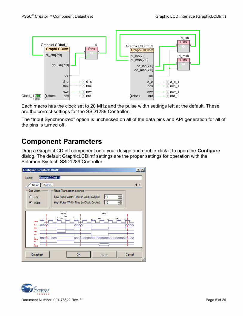
Schematic Macro InformationPSoC Creator supplies two macros in addition to the standard symbol entry in the componentcatalog. One macro is for an 8-bit implementation connected to pins and a clock. The other is fora 16-bit implementation connected to pins and a clock.
PSoC® Creator™ Component Datasheet Graphic LCD Interface (GraphicLCDIntf)
Document Number: 001-75622 Rev. ** Page 5 of 20
Each macro has the clock set to 20 MHz and the pulse width settings left at the default. Theseare the correct settings for the SSD1289 Controller.The “Input Synchronized” option is unchecked on all of the data pins and API generation for all ofthe pins is turned off.
Component ParametersDrag a GraphicLCDIntf component onto your design and double-click it to open the Configuredialog. The default GraphicLCDIntf settings are the proper settings for operation with theSolomon Systech SSD1289 Controller.
Graphic LCD Interface (GraphicLCDIntf) PSoC® Creator™ Component Datasheet
Page 6 of 20 Document Number: 001-75622 Rev. **
Bus WidthDetermines whether the component supports an 8- or 16-bit parallel interface to a graphic LCDcontroller. The default setting is 16 bit.
Low Pulse Width TimeDetermines the number of clock cycles required for the read pulse width low for the controller.This value can be set between 2 and 255 clock cycles (the minimum is 2 because the read valuemust be sampled one clock before the end of the pulse). The default setting is 10.
High Pulse Width TimeDetermines the number of clock cycles required for read pulse width high for the controller. Thisvalue can be set between 1 and 255 clock cycles. The default setting is 10.
Clock SelectionThere is no internal clock in this component. You must attach a clock source. This componentoperates from a single clock connected to the component.
PlacementThe GraphicLCDIntf is placed throughout the UDB array and all placement information isprovided to the API through the cyfitter.h file.
Resources
Resources
Resource Type API Memory (Bytes)
Pins (perExternal I/O)
DatapathCells PLDs
StatusCells Flash RAM
8-bit interface 1 4 2 109 1 12
16-bit interface 2 4 3 120 1 20
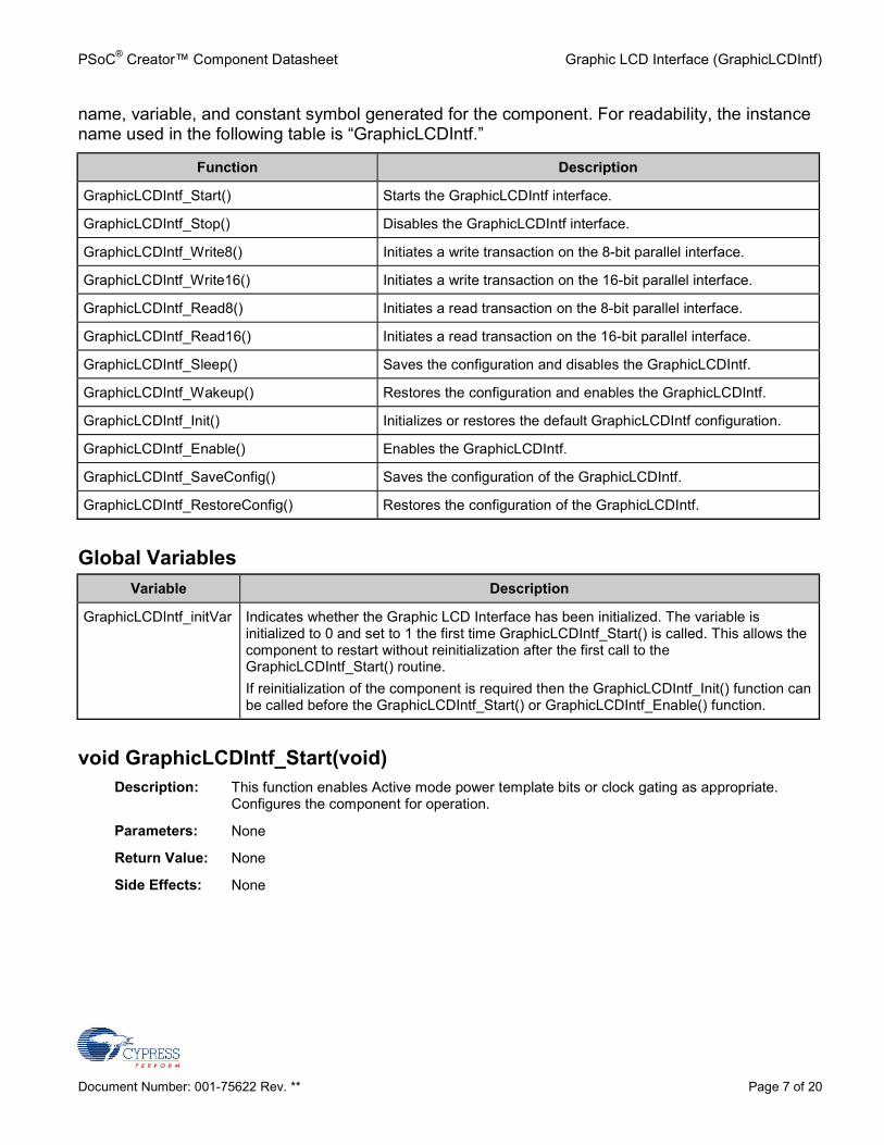
Application Programming InterfaceApplication Programming Interface (API) routines allow you to configure the component usingsoftware. The following table lists and describes the interface to each function. The subsequentsections discuss each function in more detail.By default, PSoC Creator assigns the instance name “GraphicLCDIntf_1” to the first instance ofa component in a given design. You can rename the instance to any unique value that followsthe syntactic rules for identifiers. The instance name becomes the prefix of every global function
PSoC® Creator™ Component Datasheet Graphic LCD Interface (GraphicLCDIntf)
Document Number: 001-75622 Rev. ** Page 7 of 20
name, variable, and constant symbol generated for the component. For readability, the instancename used in the following table is “GraphicLCDIntf.”
Function Description
GraphicLCDIntf_Start() Starts the GraphicLCDIntf interface.
GraphicLCDIntf_Stop() Disables the GraphicLCDIntf interface.
GraphicLCDIntf_Write8() Initiates a write transaction on the 8-bit parallel interface.
GraphicLCDIntf_Write16() Initiates a write transaction on the 16-bit parallel interface.
GraphicLCDIntf_Read8() Initiates a read transaction on the 8-bit parallel interface.
GraphicLCDIntf_Read16() Initiates a read transaction on the 16-bit parallel interface.
GraphicLCDIntf_Sleep() Saves the configuration and disables the GraphicLCDIntf.
GraphicLCDIntf_Wakeup() Restores the configuration and enables the GraphicLCDIntf.
GraphicLCDIntf_Init() Initializes or restores the default GraphicLCDIntf configuration.
GraphicLCDIntf_Enable() Enables the GraphicLCDIntf.
GraphicLCDIntf_SaveConfig() Saves the configuration of the GraphicLCDIntf.
GraphicLCDIntf_RestoreConfig() Restores the configuration of the GraphicLCDIntf.
Global VariablesVariable Description
GraphicLCDIntf_initVar Indicates whether the Graphic LCD Interface has been initialized. The variable isinitialized to 0 and set to 1 the first time GraphicLCDIntf_Start() is called. This allows thecomponent to restart without reinitialization after the first call to theGraphicLCDIntf_Start() routine.If reinitialization of the component is required then the GraphicLCDIntf_Init() function canbe called before the GraphicLCDIntf_Start() or GraphicLCDIntf_Enable() function.
void GraphicLCDIntf_Start(void)Description: This function enables Active mode power template bits or clock gating as appropriate.
Configures the component for operation.
Parameters: None
Return Value: None
Side Effects: None
Graphic LCD Interface (GraphicLCDIntf) PSoC® Creator™ Component Datasheet
Page 8 of 20 Document Number: 001-75622 Rev. **
void GraphicLCDIntf_Stop(void)Description: This function disables Active mode power template bits or gates clocks as appropriate.
Parameters: None
Return Value: None
Side Effects: None
void GraphicLCDIntf_Write8(uint8 d_c, uint8 data)Description: This function initiates a write transaction on the 8-bit parallel interface. The write is a posted
write, so this function returns before the write has actually completed on the interface. If thecommand queue is full, this function does not return until space is available to queue thiswrite request.
Parameters: d_c: Data (1) or Command (0) indication. Passed to the d_c pin
data: Data sent on the do_lsb[7:0] pins
Return Value: None
Side Effects: None
void GraphicLCDIntf_Write16(uint8 d_c, uint16 data)Description: This function initiates a write transaction on the 16-bit parallel interface. The write is a
posted write, so this function returns before the write has actually completed on theinterface. If the command queue is full, this function does not return until space is availableto queue this write request.
Parameters: d_c: Data (1) or Command (0) indication. Passed to the d_c pin
data: Data sent on the do_msb[7:0] (most significant byte) and do_lsb[7:0] (least significantbyte) pins
Return Value: None
Side Effects: None
uint8 GraphicLCDIntf_Read8(uint8 d_c)Description: This function initiates a read transaction on the 8-bit parallel interface. The read executes
after all currently posted writes have completed. This function waits until the readcompletes and then returns the read value.
Parameters: d_c: Data (1) or Command (0) indication. Passed to the d_c pin.
Return Value: 8-bit read value from the di_lsb[7:0] pins
Side Effects: None
PSoC® Creator™ Component Datasheet Graphic LCD Interface (GraphicLCDIntf)
Document Number: 001-75622 Rev. ** Page 9 of 20
uint16 GraphicLCDIntf_Read16(uint8 d_c)Description: This function initiates a read transaction on the 16-bit parallel interface. The read executes
after all currently posted writes have completed. This function waits until the readcompletes and then returns the read value.
Parameters: d_c: Data (1) or Command (0) indication. Passed to the d_c pin.
Return Value: 16-bit read value from the di_msb[7:0] (most significant byte) and di_lsb[7:0] (leastsignificant byte) pins
Side Effects: None
void GraphicLCDIntf_Sleep(void)Description: This is the preferred routine to prepare the component for sleep. The
GraphicLCDIntf_Sleep() routine saves the current component state. Then it calls theGraphicLCDIntf_Stop() function and calls GraphicLCDIntf_SaveConfig() to save thehardware configuration. Disables Active mode power template bits or clock gating asappropriate.Call the GraphicLCDIntf_Sleep() function before calling the CyPmSleep() or theCyPmHibernate() function. See the PSoC Creator System Reference Guide for moreinformation about power-management functions.
Parameters: None
Return Value: None
Side Effects: None
void GraphicLCDIntf_Wakeup(void)Description: This is the preferred routine to restore the component to the state when
GraphicLCDIntf_Sleep() was called. The GraphicLCDIntf_Wakeup() function calls theGraphicLCDIntf_RestoreConfig() function to restore the configuration. If the component wasenabled before the GraphicLCDIntf_Sleep() function was called, theGraphicLCDIntf_Wakeup() function also re-enables the component. Enables Active modepower template bits or clock gating as appropriate.
Parameters: None
Return Value: None
Side Effects: Calling the GraphicLCDIntf_Wakeup() function without first calling theGraphicLCDIntf_Sleep() or GraphicLCDIntf_SaveConfig() function can produce unexpectedbehavior.
Graphic LCD Interface (GraphicLCDIntf) PSoC® Creator™ Component Datasheet
Page 10 of 20 Document Number: 001-75622 Rev. **
void GraphicLCDIntf_Init(void)Description: This function initializes or restores the component according to the customizer Configure
dialog settings. It is not necessary to call GraphicLCDIntf_Init() because theGraphicLCDIntf_Start() routine calls this function and is the preferred method to begincomponent operation. Only the static component configuration that defines Read Low andHigh Pulse Widths will be restored to its initial values.
Parameters: None
Return Value: None
Side Effects: This reinitializes the component but it does not clear data from the FIFOs, and it does notreset the component hardware state machine. The current transaction is performed on thebus.
void GraphicLCDIntf_Enable(void)Description: This function activates the hardware and begins component operation. It is not necessary
to call GraphicLCDIntf_Enable() because the GraphicLCDIntf_Start() routine calls thisfunction, which is the preferred method to begin component operation.
Parameters: None
Return Value: None
Side Effects: None
void GraphicLCDIntf_SaveConfig(void)Description: This function saves the component configuration and nonretention registers. It also saves
the current component parameter values, as defined in the Configure dialog or as modifiedby appropriate APIs. This function is called by the GraphicLCDIntf_Sleep() function. Thecompile-time component configuration that defines read low and high pulse widths isstored.
Parameters: None
Return Value: None
Side Effects: None
PSoC® Creator™ Component Datasheet Graphic LCD Interface (GraphicLCDIntf)
Document Number: 001-75622 Rev. ** Page 11 of 20
void GraphicLCDIntf_RestoreConfig(void)Description: This function restores the configuration of GraphicLCDIntf nonretention registers. The API
is called by GraphicLCDIntf_Wakeup to restore component nonretention registers.
Parameters: None
Return Value: None
Side Effects: If this API is called before GraphicLCDIntf_SaveConfig(), the component configuration forread low and high pulse widths is restored to the values provided with the customizer.
Sample Firmware Source CodePSoC Creator provides many example projects that include schematics and example code in theFind Example Project dialog. For component-specific examples, open the dialog from theComponent Catalog or an instance of the component in a schematic. For general examples,open the dialog from the Start Page or File menu. As needed, use the Filter Options in thedialog to narrow the list of projects available to select.Refer to the “Find Example Project” topic in the PSoC Creator Help for more information..
Functional Description
Bus TransactionsThis interface can perform either a read or a write transaction. These transactions have thefollowing parameters:
Read or write
Address: In this case it is a one bit address driven on the d_c pin
Data (8 or 16 bits): Sent on “do” for writes and read on “di” for reads.The implementation assumes that the CPU sends a command byte to the component using aFIFO (the same FIFO that is used for data). That command byte indicates read or write andprovides the d_c bit.
Idle ConditionWhen neither a read nor a write is occurring on the interface, the interface is in the idle state.The values for the output pins in that condition are:
d_c: Don’t care (may be left at its last state)
ncs: 1
Graphic LCD Interface (GraphicLCDIntf) PSoC® Creator™ Component Datasheet
Page 12 of 20 Document Number: 001-75622 Rev. **
nwr: 1
nrd: 1
do: Don’t care (may be left at its last state)
oe: 0In the description of the read and write transactions, any signal not listed is idle.
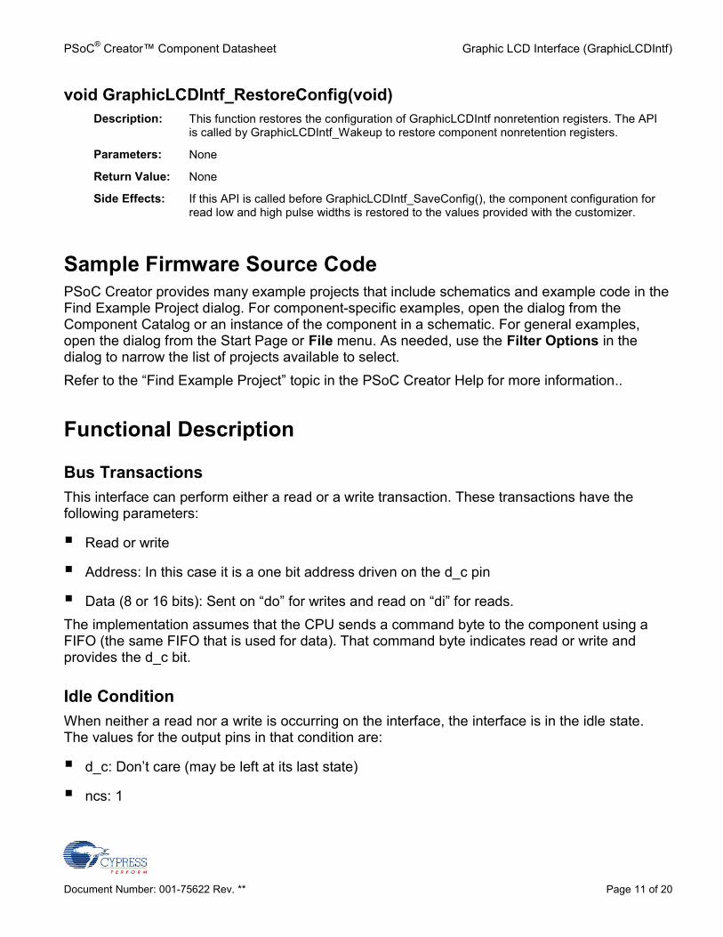
Write TransactionFigure 1 shows the timing diagram for a write transaction on the parallel interface.
Figure 1. Write Transaction Timing Diagram
d_c
ncs
nwr
do
oe
This diagram shows that the write transaction requires three clock cycles. The timing diagram isthe same regardless of the bit width. This transaction can be immediately preceded or followedby another read or write transaction or may be in the idle state before or after a write transaction.The interface to the CPU allows the CPU to make posted write requests (request a writeproviding the address and data and then proceed before the transaction is actually completed onparallel bus). The implementation allows the CPU to have two write requests outstanding withoutstalling.
PSoC® Creator™ Component Datasheet Graphic LCD Interface (GraphicLCDIntf)
Document Number: 001-75622 Rev. ** Page 13 of 20
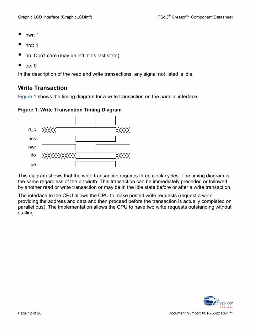
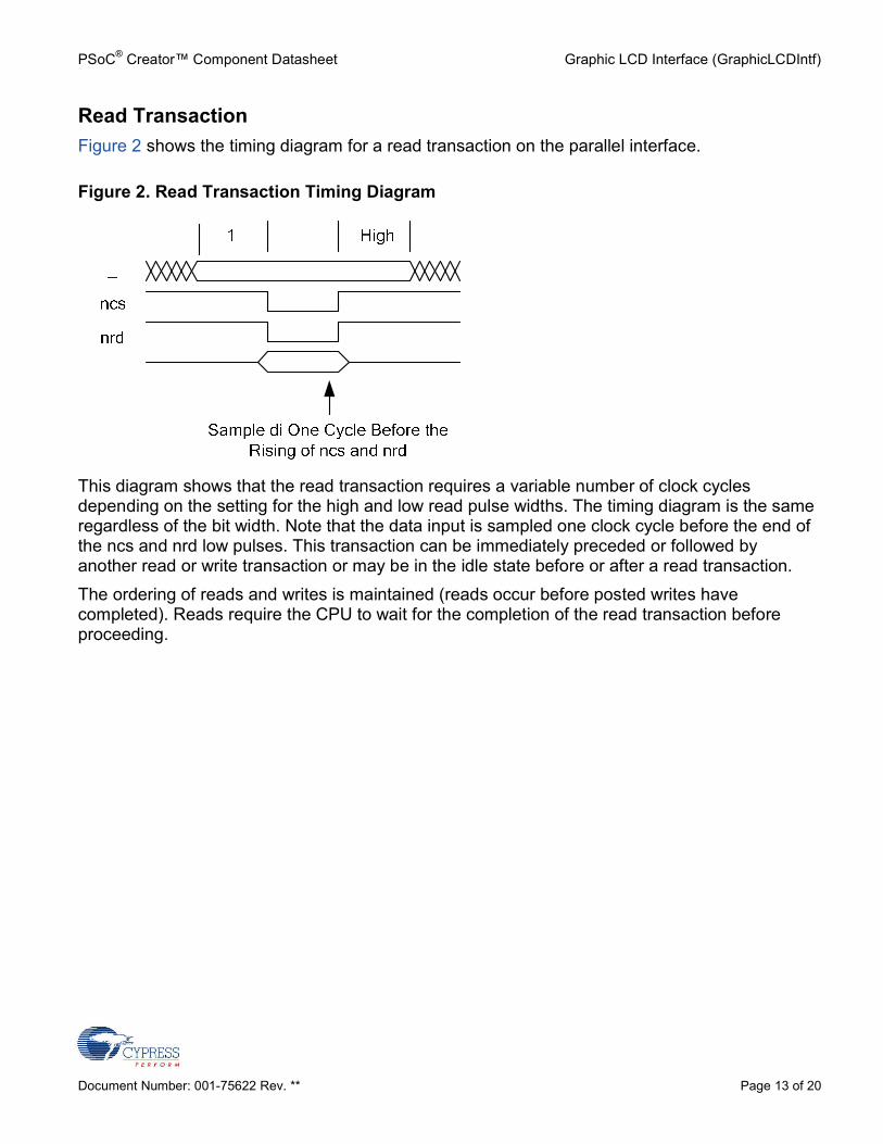
Read TransactionFigure 2 shows the timing diagram for a read transaction on the parallel interface.
Figure 2. Read Transaction Timing Diagram
This diagram shows that the read transaction requires a variable number of clock cyclesdepending on the setting for the high and low read pulse widths. The timing diagram is the sameregardless of the bit width. Note that the data input is sampled one clock cycle before the end ofthe ncs and nrd low pulses. This transaction can be immediately preceded or followed byanother read or write transaction or may be in the idle state before or after a read transaction.The ordering of reads and writes is maintained (reads occur before posted writes havecompleted). Reads require the CPU to wait for the completion of the read transaction beforeproceeding.
Graphic LCD Interface (GraphicLCDIntf) PSoC® Creator™ Component Datasheet
Page 14 of 20 Document Number: 001-75622 Rev. **
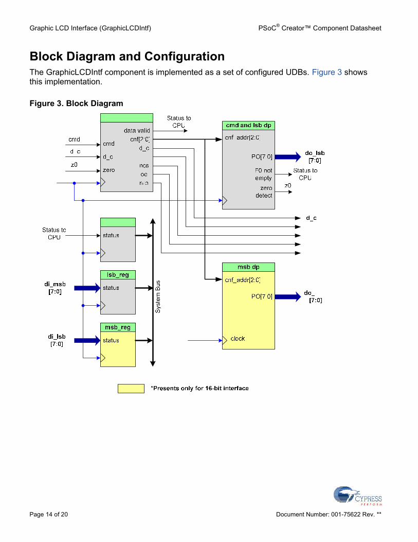
Block Diagram and ConfigurationThe GraphicLCDIntf component is implemented as a set of configured UDBs. Figure 3 showsthis implementation.
Figure 3. Block Diagram
PSoC® Creator™ Component Datasheet Graphic LCD Interface (GraphicLCDIntf)
Document Number: 001-75622 Rev. ** Page 15 of 20
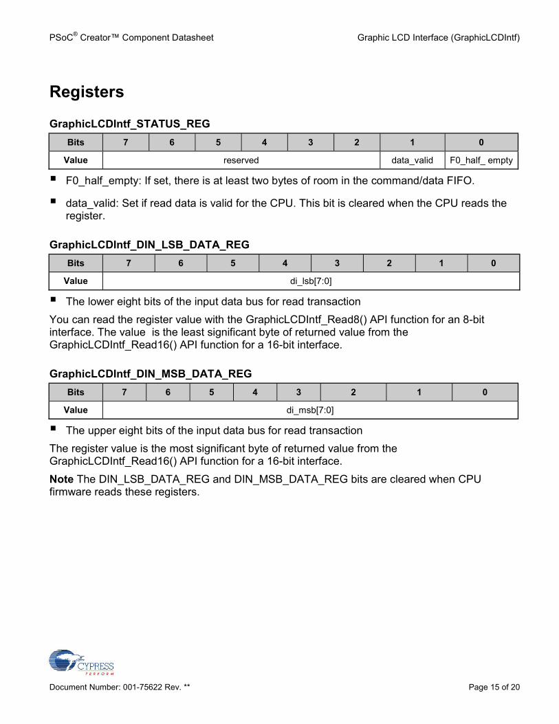
Registers
GraphicLCDIntf_STATUS_REGBits 7 6 5 4 3 2 1 0
Value reserved data_valid F0_half_ empty
F0_half_empty: If set, there is at least two bytes of room in the command/data FIFO.
data_valid: Set if read data is valid for the CPU. This bit is cleared when the CPU reads theregister.
GraphicLCDIntf_DIN_LSB_DATA_REGBits 7 6 5 4 3 2 1 0
Value di_lsb[7:0]
The lower eight bits of the input data bus for read transactionYou can read the register value with the GraphicLCDIntf_Read8() API function for an 8-bitinterface. The value is the least significant byte of returned value from theGraphicLCDIntf_Read16() API function for a 16-bit interface.
GraphicLCDIntf_DIN_MSB_DATA_REGBits 7 6 5 4 3 2 1 0
Value di_msb[7:0]
The upper eight bits of the input data bus for read transactionThe register value is the most significant byte of returned value from theGraphicLCDIntf_Read16() API function for a 16-bit interface.Note The DIN_LSB_DATA_REG and DIN_MSB_DATA_REG bits are cleared when CPUfirmware reads these registers.
Graphic LCD Interface (GraphicLCDIntf) PSoC® Creator™ Component Datasheet
Page 16 of 20 Document Number: 001-75622 Rev. **
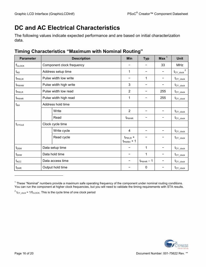
DC and AC Electrical CharacteristicsThe following values indicate expected performance and are based on initial characterizationdata.
Timing Characteristics “Maximum with Nominal Routing”Parameter Description Min Typ Max 1 Unit
fCLOCK Component clock frequency − − 33 MHz
tAS Address setup time 1 − − tCY_clock2
tPWLW Pulse width low write − 1 − tCY_clock
tPWHW Pulse width high write 3 − − tCY_clock
tPWLR Pulse width low read 2 − 255 tCY_clock
tPWHR Pulse width high read 1 − 255 tCY_clock
tAH Address hold time
Write 2 − − tCY_clock
Read tPWHR − − tCY_clock
tCYCLE Clock cycle time
Write cycle 4 − − tCY_clock
Read cycle tPWLR +tPWRH + 1
− − tCY_clock
tDSW Data setup time − 1 − tCY_clock
tDHW Data hold time − 1 − tCY_clock
tACC Data access time − tPWHR – 1 − tCY_clock
tDHR Output hold time − 0 − tCY_clock
1 These “Nominal” numbers provide a maximum safe operating frequency of the component under nominal routing conditions.You can run the component at higher clock frequencies, but you will need to validate the timing requirements with STA results.2 tCY_clock = 1/fCLOCK. This is the cycle time of one clock period
PSoC® Creator™ Component Datasheet Graphic LCD Interface (GraphicLCDIntf)
Document Number: 001-75622 Rev. ** Page 17 of 20
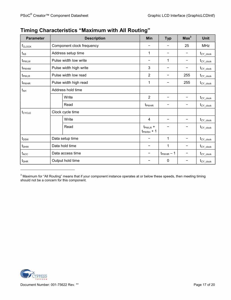
Timing Characteristics “Maximum with All Routing”Parameter Description Min Typ Max3 Unit
fCLOCK Component clock frequency − − 25 MHz
tAS Address setup time 1 − − tCY_clock
tPWLW Pulse width low write − 1 − tCY_clock
tPWHW Pulse width high write 3 − − tCY_clock
tPWLR Pulse width low read 2 − 255 tCY_clock
tPWHR Pulse width high read 1 − 255 tCY_clock
tAH Address hold time
Write 2 − − tCY_clock
Read tPWHR − − tCY_clock
tCYCLE Clock cycle time
Write 4 − − tCY_clock
Read tPWLR +tPWRH + 1
− − tCY_clock
tDSW Data setup time − 1 − tCY_clock
tDHW Data hold time − 1 − tCY_clock
tACC Data access time − tPWHR – 1 − tCY_clock
tDHR Output hold time − 0 − tCY_clock
3 Maximum for “All Routing” means that if your component instance operates at or below these speeds, then meeting timingshould not be a concern for this component.
Graphic LCD Interface (GraphicLCDIntf) PSoC® Creator™ Component Datasheet
Page 18 of 20 Document Number: 001-75622 Rev. **
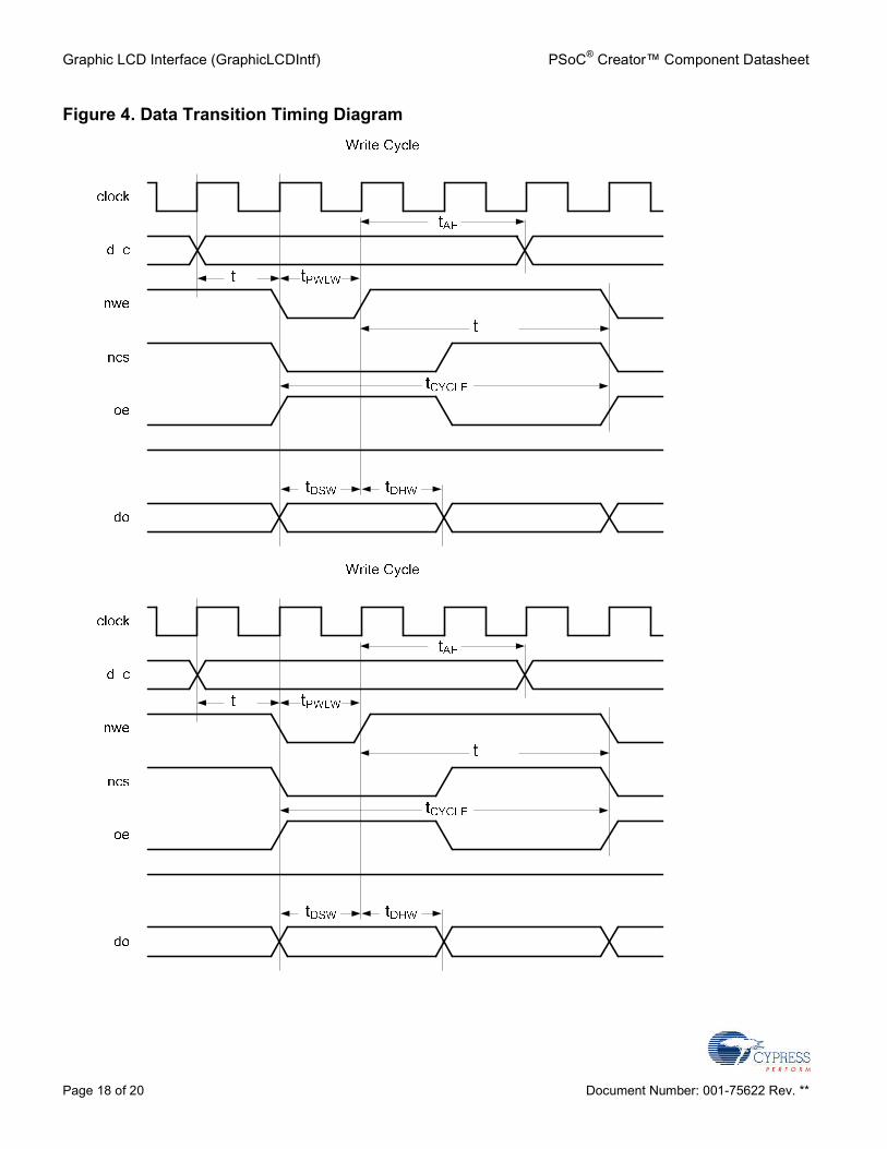
Figure 4. Data Transition Timing Diagram
PSoC® Creator™ Component Datasheet Graphic LCD Interface (GraphicLCDIntf)
Document Number: 001-75622 Rev. ** Page 19 of 20
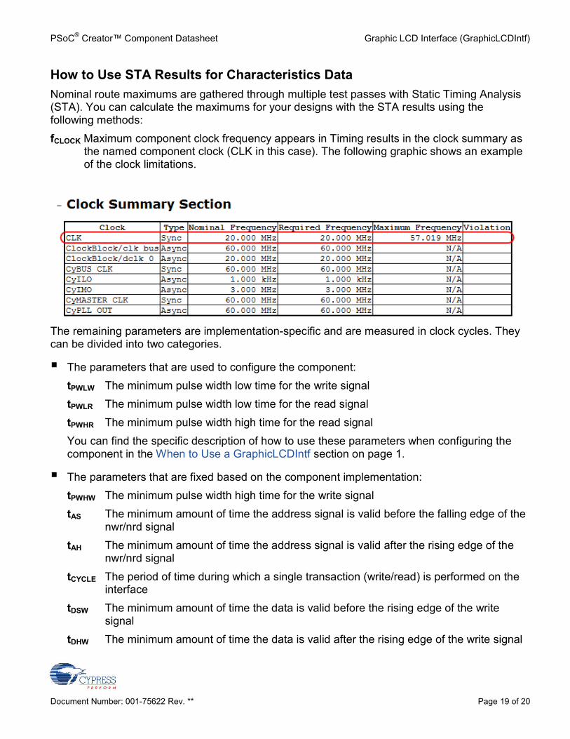
How to Use STA Results for Characteristics DataNominal route maximums are gathered through multiple test passes with Static Timing Analysis(STA). You can calculate the maximums for your designs with the STA results using thefollowing methods:fCLOCK Maximum component clock frequency appears in Timing results in the clock summary as
the named component clock (CLK in this case). The following graphic shows an exampleof the clock limitations.
The remaining parameters are implementation-specific and are measured in clock cycles. Theycan be divided into two categories.
The parameters that are used to configure the component:tPWLW The minimum pulse width low time for the write signaltPWLR The minimum pulse width low time for the read signaltPWHR The minimum pulse width high time for the read signalYou can find the specific description of how to use these parameters when configuring thecomponent in the When to Use a GraphicLCDIntf section on page 1.
The parameters that are fixed based on the component implementation:tPWHW The minimum pulse width high time for the write signaltAS The minimum amount of time the address signal is valid before the falling edge of the
nwr/nrd signaltAH The minimum amount of time the address signal is valid after the rising edge of the
nwr/nrd signaltCYCLE The period of time during which a single transaction (write/read) is performed on the
interfacetDSW The minimum amount of time the data is valid before the rising edge of the write
signaltDHW The minimum amount of time the data is valid after the rising edge of the write signal
Graphic LCD Interface (GraphicLCDIntf) PSoC® Creator™ Component Datasheet
Page 20 of 20 Document Number: 001-75622 Rev. **
tACC The minimum amount of time the data is sampled after the negative edge of the readsignal
tDHR The minimum amount of time the data should be valid after rising edge of the nrdsignal
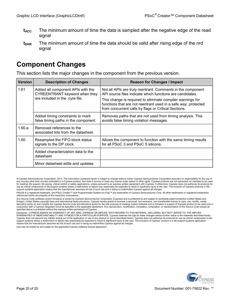
Component ChangesThis section lists the major changes in the component from the previous version.
Version Description of Changes Reason for Changes / Impact
1.61 Added all component APIs with theCYREENTRANT keyword when theyare included in the .cyre file.
Not all APIs are truly reentrant. Comments in the componentAPI source files indicate which functions are candidates.This change is required to eliminate compiler warnings forfunctions that are not reentrant used in a safe way: protectedfrom concurrent calls by flags or Critical Sections.
Added timing constraints to markfalse timing paths in the component.
Removes paths that are not used from timing analysis. Thisavoids false timing violation messages.
1.60.a Removed references to theassociated kits from the datasheet.
1.60 Resampled the FIFO block statussignals to the DP clock.
Allows the component to function with the same timing resultsfor all PSoC 3 and PSoC 5 silicons.
Added characterization data to thedatasheet
Minor datasheet edits and updates
© Cypress Semiconductor Corporation, 2012. The information contained herein is subject to change without notice. Cypress Semiconductor Corporation assumes no responsibility for the use ofany circuitry other than circuitry embodied in a Cypress product. Nor does it convey or imply any license under patent or other rights. Cypress products are not warranted nor intended to be usedfor medical, life support, life saving, critical control or safety applications, unless pursuant to an express written agreement with Cypress. Furthermore, Cypress does not authorize its products foruse as critical components in life-support systems where a malfunction or failure may reasonably be expected to result in significant injury to the user. The inclusion of Cypress products in life-support systems application implies that the manufacturer assumes all risk of such use and in doing so indemnifies Cypress against all charges.PSoC® is a registered trademark, and PSoC Creator™ and Programmable System-on-Chip™ are trademarks of Cypress Semiconductor Corp. All other trademarks or registered trademarksreferenced herein are property of the respective corporations.Any Source Code (software and/or firmware) is owned by Cypress Semiconductor Corporation (Cypress) and is protected by and subject to worldwide patent protection (United States andforeign), United States copyright laws and international treaty provisions. Cypress hereby grants to licensee a personal, non-exclusive, non-transferable license to copy, use, modify, createderivative works of, and compile the Cypress Source Code and derivative works for the sole purpose of creating custom software and or firmware in support of licensee product to be used only inconjunction with a Cypress integrated circuit as specified in the applicable agreement. Any reproduction, modification, translation, compilation, or representation of this Source Code except asspecified above is prohibited without the express written permission of Cypress.Disclaimer: CYPRESS MAKES NO WARRANTY OF ANY KIND, EXPRESS OR IMPLIED, WITH REGARD TO THIS MATERIAL, INCLUDING, BUT NOT LIMITED TO, THE IMPLIEDWARRANTIES OF MERCHANTABILITY AND FITNESS FOR A PARTICULAR PURPOSE. Cypress reserves the right to make changes without further notice to the materials described herein.Cypress does not assume any liability arising out of the application or use of any product or circuit described herein. Cypress does not authorize its products for use as critical components in life-support systems where a malfunction or failure may reasonably be expected to result in significant injury to the user. The inclusion of Cypress’ product in a life-support systems applicationimplies that the manufacturer assumes all risk of such use and in doing so indemnifies Cypress against all charges.Use may be limited by and subject to the applicable Cypress software license agreement.
Related Documents