Graphene From Wikipedia, the free encyclopedia Jump to: navigation , search Not to be confused with Grapheme , Graphane , or Graphyne . This article may be too technical for most readers to understand. Please help improve this article to make it understandable to non-experts , without removing the technical details. The talk page may contain suggestions. (December 2013) Graphene is an atomic-scale honeycomb lattice made of carbon atoms. Graphene is a 2-dimensional, crystaline allotrope of carbon . In graphene carbon atoms are densely packed in a regular sp 2 -bonded atomic-scale chicken wire (hexagonal ) pattern. Graphene can be described as a one-atom thick layer of graphite . It is the basic structural element of other allotropes, including graphite, charcoal , carbon nanotubes and fullerenes . It can also be considered as an indefinitely large aromatic molecule, the limiting case of the family of flat polycyclic aromatic hydrocarbons . High-quality graphene is strong, light, nearly transparent and an excellent conductor of heat and electricity. Its interactions with other materials and with light and its inherently two- dimensional nature produce unique properties, such as the bipolar

Graphene-A 2 Dimensional Material
Oct 24, 2015
Graphene-a 2 dimensional material
Welcome message from author
This document is posted to help you gain knowledge. Please leave a comment to let me know what you think about it! Share it to your friends and learn new things together.
Transcript
GrapheneFrom Wikipedia, the free encyclopediaJump to: navigation, search Not to be confused with Grapheme, Graphane, or Graphyne.
This article may be too technical for most readers to understand. Please help improve this article to make it understandable to non-experts, without removing the technical details. The talk page may contain suggestions. (December 2013)
Graphene is an atomic-scale honeycomb lattice made of carbon atoms.
Graphene is a 2-dimensional, crystaline allotrope of carbon. In graphene carbon atoms are densely packed in a regular sp 2 -bonded atomic-scale chicken wire (hexagonal) pattern. Graphene can be described as a one-atom thick layer of graphite. It is the basic structural element of other allotropes, including graphite, charcoal, carbon nanotubes and fullerenes. It can also be considered as an indefinitely large aromatic molecule, the limiting case of the family of flat polycyclic aromatic hydrocarbons.
High-quality graphene is strong, light, nearly transparent and an excellent conductor of heat and electricity. Its interactions with other materials and with light and its inherently two-dimensional nature produce unique properties, such as the bipolar transistor effect, ballistic transport of charges and large quantum oscillations.
At the time of its isolation in 2004,[1] many researchers studying carbon nanotubes were already familiar with graphene's composition, structure and properties, which had been calculated decades earlier.
The combination of familiarity, extraordinary properties and surprising ease of isolation enabled a rapid increase in graphene research. Andre Geim and Konstantin Novoselov at the University of Manchester won the Nobel Prize in Physics in 2010 "for groundbreaking experiments regarding the two-dimensional material graphene".[2]

Contents
1 Definition 2 History 3 Properties
o 3.1 Structure o 3.2 Physical o 3.3 Electronic o 3.4 Optical o 3.5 Excitonic o 3.6 Thermal o 3.7 Mechanical o 3.8 Spin transport o 3.9 Anomalous quantum Hall effect
4 Forms o 4.1 Nanostripes o 4.2 Graphene oxide o 4.3 Chemical modification o 4.4 Casimir effect and dispersion o 4.5 Bilayer graphene o 4.6 3D graphene
5 Production techniques o 5.1 Exfoliation o 5.2 Epitaxy o 5.3 Reduction o 5.4 Metal-carbon melts o 5.5 Sodium ethoxide pyrolysis o 5.6 Nanotube slicing o 5.7 Graphite sonication o 5.8 Carbon dioxide reduction
6 Potential applications o 6.1 Medicine o 6.2 Integrated circuits o 6.3 Redox o 6.4 Transparent conducting electrodes o 6.5 Ethanol distillation o 6.6 Desalination o 6.7 Solar cells o 6.8 Single-molecule gas detection o 6.9 Quantum dots o 6.10 Frequency multiplier o 6.11 Optical modulator o 6.12 Coolant additive o 6.13 Reference material o 6.14 Thermal management
o 6.15 Energy storage o 6.16 Engineered piezoelectricity o 6.17 Biodevice
7 Pseudo-relativistic theory 8 See also 9 References 10 Sources 11 External links
Definition
"Graphene" is a combination of graphite and the suffix -ene, named by Hanns-Peter Boehm,[3] who described single-layer carbon foils in 1962.[4]
The term graphene first appeared in 1987[5] to describe single sheets of graphite as one of the constituents of graphite intercalation compounds (GICs); conceptually a GIC is a crystalline salt of the intercalant and graphene. The term was also used in early descriptions of carbon nanotubes,[6] as well as for epitaxial graphene[7] and polycyclic aromatic hydrocarbons.[8]
The IUPAC compendium of technology states: "previously, descriptions such as graphite layers, carbon layers, or carbon sheets have been used for the term graphene... it is incorrect to use for a single layer a term which includes the term graphite, which would imply a three-dimensional structure. The term graphene should be used only when the reactions, structural relations or other properties of individual layers are discussed."[9]
Graphene can be considered an "infinite alternant" (only six-member carbon ring) polycyclic aromatic hydrocarbon (PAH). The largest known isolated PAH molecule consists of 222 atoms and is 10 benzene rings across.[10] It has proven difficult to synthesize even slightly bigger molecules, and they still remain "a dream of many organic and polymer chemists".[11]
A definition of "isolated or free-standing graphene" was proposed: "graphene is a single atomic plane of graphite, which – and this is essential – is sufficiently isolated from its environment to be considered free-standing."[12] This definition is narrower than the definition given above and refers to cleaved, transferred and suspended graphene monolayers.[citation needed] Other forms of graphene, such as graphene grown on various metals, can become free-standing if, for example, suspended or transferred to silicon dioxide (SiO2) or silicon carbide (after its passivation with hydrogen).[13]
History
In 1859 Benjamin Collins Brodie was aware of the highly lamellar structure of thermally reduced graphite oxide.[14]
The structure of graphite was solved in 1916.[15] by the related method of powder diffraction,[16][17]
It was studied in detail by V. Kohlschütter and P. Haenni in 1918, who also described the
properties of graphite oxide paper.[18] Its structure was determined from single-crystal diffraction in 1924.[19][20]
The theory of graphene was first explored by P. R. Wallace in 1947 as a starting point for understanding the electronic properties of 3D graphite. The emergent massless Dirac equation was first pointed out by Gordon Walter Semenoff and David P. DeVincenzo and Eugene J. Mele.[21] Semenoff emphasized the occurrence in a magnetic field of an electronic Landau level precisely at the Dirac point. This level is responsible for the anomalous integer quantum Hall effect.[22][23][24]
The earliest TEM images of few-layer graphite were published by G. Ruess and F. Vogt in 1948.[25] Later, single graphene layers were also observed directly by electron microscopy.[26] Before 2004 intercalated graphite compounds were studied under a transmission electron microscope (TEM). Researchers occasionally observed thin graphitic flakes ("few-layer graphene") and possibly even individual layers. An early, detailed study on few-layer graphite dates to 1962.[27]
[28]
Starting in the 1970s single layers of graphite were grown epitaxially on top of other materials.[29]
This "epitaxial graphene" consists of a single-atom-thick hexagonal lattice of sp 2 -bonded carbon atoms, as in free-standing graphene. However, there is significant charge transfer from the substrate to the epitaxial graphene, and, in some cases, hybridization between the d-orbitals of the substrate atoms and π orbitals of graphene, which significantly alters the electronic structure of epitaxial graphene.
Single layers of graphite were also observed by transmission electron microscopy within bulk materials, in particular inside soot obtained by chemical exfoliation. Efforts to make thin films of graphite by mechanical exfoliation started in 1990,[30] but nothing thinner than 50 to 100 layers was produced before 2004.
A lump of graphite, a graphene transistor and a tape dispenser. Donated to the Nobel Museum in Stockholm by Andre Geim and Konstantin Novoselov in 2010.
Initial attempts to make atomically thin graphitic films employed exfoliation techniques similar to the drawing method. Multilayer samples down to 10 nm in thickness were obtained.[31] Old papers were unearthed[27] in which researchers tried to isolate graphene starting with intercalated compounds. These papers reported the observation of very thin graphitic fragments (possibly monolayers) by transmission electron microscopy. Neither of the earlier observations was
sufficient to "spark the graphene gold rush", which awaited macroscopic samples of extracted atomic planes.
In 2004 Andre Geim and Kostya Novoselov at University of Manchester extracted single-atom-thick crystallites from bulk graphite in 2004.[32] They pulled graphene layers from graphite and transferred them onto thin SiO2 on a silicon wafer in a process called either micromechanical cleavage or the Scotch tape technique. The SiO2 electrically isolated the graphene and weakly interacted with it, providing nearly charge-neutral graphene layers. The silicon beneath the SiO2 could be used as a "back gate" electrode to vary the charge density in the graphene over a wide range. They may not have been the first to use this technique—patent 6667100 US, filed in 2002, describes how to process commercially available flexible expanded graphite to achieve a graphite thickness of 0.01 thousandth of an inch. The key to success was high-throughput visual recognition of graphene on a properly chosen substrate, which provides a small but noticeable optical contrast.
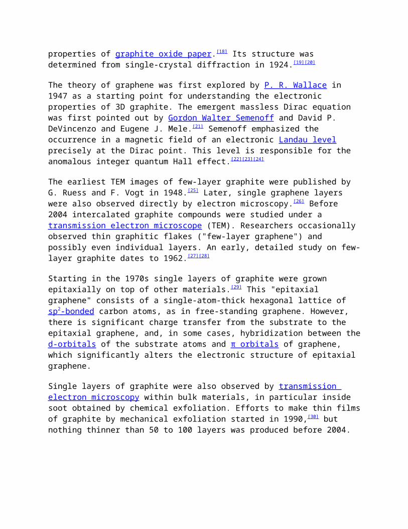
The cleavage technique led directly to the first observation of the anomalous quantum Hall effect in graphene,[22][24] which provided direct evidence of graphene's theoretically predicted Berry's phase of massless Dirac fermions. The effect was reported soon after by Philip Kim and Yuanbo Zhang in 2005. These experiments started after the researchers observed colleagues who were looking for the quantum Hall effect[33] and Dirac fermions[34] in bulk graphite.
Even though graphene on nickel and on silicon carbide have both existed in the laboratory for decades, graphene mechanically exfoliated on SiO2 provided the first proof of the Dirac fermion nature of electrons.[citation needed]
Andre Geim and Konstantin Novoselov, 2010
Geim and Novoselev received several awards for their pioneering research on graphene, notably the 2010 Nobel Prize in Physics.[35]
Properties
Structure

The atomic structure of isolated, single-layer graphene was studied by transmission electron microscopy (TEM) on sheets of graphene suspended between bars of a metallic grid.[26] Electron diffraction patterns showed the expected honeycomb lattice. Suspended graphene also showed "rippling" of the flat sheet, with amplitude of about one nanometer. These ripples may be intrinsic to the material as a result of the instability of two-dimensional crystals,[31][36][37] or may originate from the ubiquitous dirt seen in all TEM images of graphene. Atomic resolution real-space images of isolated, single-layer graphene on SiO2 substrates are available[38][39] via scanning tunneling microscopy. Photoresist residue, which must be removed to obtain atomic-resolution images, may be the "adsorbates" observed in TEM images, and may explain the observed rippling. Rippling on SiO2 is caused by conformation of graphene to the underlying SiO2, and is not intrinsic.[38]
Graphene sheets in solid form usually show evidence in diffraction for graphite's (002) layering. This is true of some single-walled nanostructures.[40] However, unlayered graphene with only (hk0) rings has been found in the core of presolar graphite onions.[41] TEM studies show faceting at defects in flat graphene sheets[42] and suggest a role for two-dimensional crystallization from a melt.
Graphene can self-repair holes in its sheets, when exposed to molecules containing carbon, such as hydrocarbons. Bombarded with pure carbon atoms, the atoms perfectly align into hexagons, completely filling the holes.[43][44]
Physical
The carbon–carbon bond length in graphene is about 0.142 nanometers.[45] Graphene sheets stack to form graphite with an interplanar spacing of 0.335 nm.
Electronic
GNR band structure for zig-zag orientation. Tightbinding calculations show that zigzag orientation is always metallic.
GNR band structure for arm-chair orientation. Tightbinding calculations show that armchair orientation can be semiconducting or metallic depending on width (chirality).
Graphene differs from most three-dimensional materials. Intrinsic graphene is a semi-metal or zero-gap semiconductor. Understanding the electronic structure of graphene is the starting point for finding the band structure of graphite. The energy-momentum relation (dispersion relation) is linear for low energies near the six corners of the two-dimensional hexagonal Brillouin zone, leading to zero effective mass for electrons and holes.[46] Due to this linear (or “conical") dispersion relation at low energies, electrons and holes near these six points, two of which are inequivalent, behave like relativistic particles described by the Dirac equation for spin-1/2 particles.[47][48] Hence, the electrons and holes are called Dirac fermions and the six corners of the Brillouin zone are called the Dirac points.[47] The equation describing the electrons' linear
dispersion relation is ; where the Fermi velocity vF ~ 106 m/s, and the wavevector k is measured from the Dirac points (the zero of energy is chosen here to coincide with the Dirac points).[48]
Electron transport
Experimental results from transport measurements show that graphene has a remarkably high electron mobility at room temperature, with reported values in excess of 15,000 cm2·V−1·s−1.[31] Additionally, the symmetry of the experimentally measured conductance indicates that hole and electron mobilities should be nearly the same.[46] The mobility is nearly independent of temperature between 10 K and 100 K,[22][49][50] which implies that the dominant scattering mechanism is defect scattering. Scattering by the acoustic phonons of graphene intrinsically limits room temperature mobility to 200,000 cm2·V−1·s−1 at a carrier density of 1012 cm−2.[50][51] The corresponding resistivity of the graphene sheet would be 10−6 Ω·cm. This is less than the resistivity of silver, the lowest known at room temperature.[52] However, for graphene on SiO2 substrates, scattering of electrons by optical phonons of the substrate is a larger effect at room

temperature than scattering by graphene’s own phonons. This limits mobility to 40,000 cm2·V−1·s−1.[50]
Despite zero carrier density near the Dirac points, graphene exhibits a minimum conductivity on
the order of . The origin of this minimum conductivity is still unclear. However, rippling of the graphene sheet or ionized impurities in the SiO2 substrate may lead to local puddles of carriers that allow conduction.[46] Several theories
suggest that the minimum conductivity should be ; however, most measurements are
of order or greater[31] and depend on impurity concentration.[53]
Graphene doped with various gaseous species (both acceptors and donors) can be returned to an undoped state by gentle heating in vacuum.[53][54] Even for dopant concentrations in excess of 1012
cm2 carrier mobility exhibits no observable change.[54] Graphene doped with potassium in ultra-high vacuum at low temperature can reduce mobility 20-fold.[53][55] The mobility reduction is reversible on heating the graphene to remove the potassium.
Due to graphene's two dimensions, charge fractionalization (where the apparent charge of individual pseudoparticles in low-dimensional systems is less than a single quantum[56]) is thought to occur. It may therefore be a suitable material for constructing quantum computers [57] using anyonic circuits.[58]
Optical
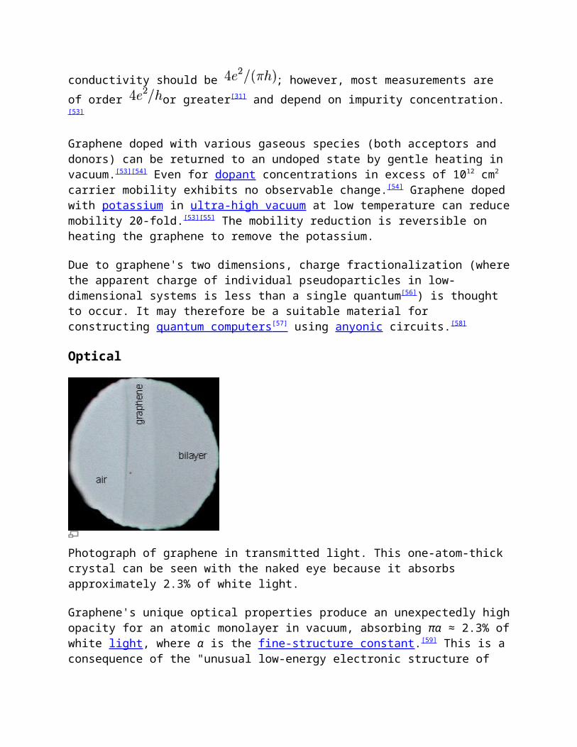
Photograph of graphene in transmitted light. This one-atom-thick crystal can be seen with the naked eye because it absorbs approximately 2.3% of white light.
Graphene's unique optical properties produce an unexpectedly high opacity for an atomic monolayer in vacuum, absorbing πα ≈ 2.3% of white light, where α is the fine-structure constant.[59] This is a consequence of the "unusual low-energy electronic structure of monolayer graphene that features electron and hole conical bands meeting each other at the Dirac point... [which] is qualitatively different from more common quadratic massive bands".[60] Based on the Slonczewski–Weiss–McClure (SWMcC) band model of graphite, the interatomic distance,

hopping value and frequency cancel when optical conductance is calculated using Fresnel equations in the thin-film limit.
Although confirmed experimentally, the measurement is not precise enough to improve on other techniques for determining the fine-structure constant.[61]
Graphene's band gap can be tuned from 0 to 0.25 eV (about 5 micrometre wavelength) by applying voltage to a dual-gate bilayer graphene field-effect transistor (FET) at room temperature.[62] The optical response of graphene nanoribbons is tunable into the terahertz regime by an applied magnetic field.[63] Graphene/graphene oxide systems exhibit electrochromic behavior, allowing tuning of both linear and ultrafast optical properties.[64]
A graphene-based Bragg grating (one-dimensional photonic crystal) has been fabricated and demonstrated its capability for excitation of surface electromagnetic waves in the periodic structure by using 633 nm He-Ne laser as the light source.[65]
Saturable absorption
Such unique absorption could become saturated when the input optical intensity is above a threshold value. This nonlinear optical behavior is termed saturable absorption and the threshold value is called the saturation fluence. Graphene can be saturated readily under strong excitation over the visible to near-infrared region, due to the universal optical absorption and zero band gap. This has relevance for the mode locking of fiber lasers, where fullband mode locking has been achieved by graphene-based saturable absorber. Due to this special property, graphene has wide application in ultrafast photonics. Moreover, the optical response of graphene/graphene oxide layers can be tuned electrically.[64][66] Saturable absorption in graphene could occur at the Microwave and Terahertz band, owing to its wideband optical absorption property. The microwave saturable absorption in graphene demonstrates the possibility of graphene microwave and terahertz photonics devices, such as microwave saturable absorber, modulator, polarizer, microwave signal processing and broad-band wireless access networks.[67]
Nonlinear Kerr effect
Under more intensive laser illumination, graphene could also possess a nonlinear phase shift due to the optical nonlinear Kerr effect. Based on a typical open and close aperture z-scan measurement, graphene possesses a giant non-linear Kerr coefficient of 10−7 cm2·W−1, almost nine orders of magnitude larger than that of bulk dielectrics.[68] This suggests that graphene may be a nonlinear Kerr medium, paving the way for graphene-based nonlinear Kerr photonics such as a soliton.
Excitonic
First-principle calculations with quasiparticle corrections and many-body effects are performed to study the electronic and optical properties of graphene-based materials. The approach is described as three stages.[69] With GW calculation, the properties of graphene-based materials are accurately investigated, including graphene,[70] graphene nanoribbons,[71] edge and surface
functionalized armchair graphene nanoribbons,[72] hydrogen saturated armchair graphene nanoribbons,[73] Josephson effect in graphene SNS junctions with single localized defect[74] and scaling properties in armchair graphene nanoribbons.[75]
Thermal
Stability
Ab initio calculations show that a graphene sheet is thermodynamically unstable if its size is less than about 20 nm (“graphene is the least stable structure until about 6000 atoms”) and becomes the most stable fullerene (as within graphite) only for molecules larger than 24,000 atoms.[76]
Conductivity
The near-room temperature thermal conductivity of graphene was measured to be between (4.84±0.44) × 103 to (5.30±0.48) × 103 W·m−1·K−1. These measurements, made by a non-contact optical technique, are in excess of those measured for carbon nanotubes or diamonds. The isotopic composition, the ratio of 12 C to 13 C , has a significant impact on thermal conductivity, where isotopically pure 12C graphene has higher conductivity than either a 50:50 isotope ratio or the naturally occurring 99:1 ratio.[77] It can be shown by using the Wiedemann–Franz law, that the thermal conduction is phonon-dominated.[78] However, for a gated graphene strip, an applied gate bias causing a Fermi energy shift much larger than kBT can cause the electronic contribution to increase and dominate over the phonon contribution at low temperatures. The ballistic thermal conductance of graphene is isotropic.[79][80]
Potential for this high conductivity can be seen by considering graphite, a 3D version of graphene that has basal plane thermal conductivity of over a 1,000 W·m−1·K−1 (comparable to diamond). In graphite, the c-axis (out of plane) thermal conductivity is over a factor of ~100 smaller due to the weak binding forces between basal planes as well as the larger lattice spacing.[81] In addition, the ballistic thermal conductance of a graphene is shown to give the lower limit of the ballistic thermal conductances, per unit circumference, length of carbon nanotubes.[82]
Despite its 2-D nature, graphene has 3 acoustic phonon modes. The two in-plane modes (LA, TA) have a linear dispersion relation, whereas the out of plane mode (ZA) has a quadratic dispersion relation. Due to this, the T2 dependent thermal conductivity contribution of the linear modes is dominated at low temperatures by the T1.5 contribution of the out of plane mode.[82] Some graphene phonon bands display negative Grüneisen parameters.[83] At low temperatures (where most optical modes with positive Grüneisen parameters are still not excited) the contribution from the negative Grüneisen parameters will be dominant and thermal expansion coefficient (which is directly proportional to Grüneisen parameters) negative. The lowest negative Grüneisen parameters correspond to the lowest transversal acoustic ZA modes. Phonon frequencies for such modes increase with the in-plane lattice parameter since atoms in the layer upon stretching will be less free to move in the z direction. This is similar to the behavior of a string, which, when it is stretched, will have vibrations of smaller amplitude and higher frequency. This phenomenon, named "membrane effect", was predicted by Lifshitz in 1952.[84]
Mechanical
The flat graphene sheet is unstable with respect to scrolling i.e. bending into a cylindrical shape, which is its lower-energy state.[85]
As of 2009, graphene appeared to be one of the strongest materials known with a breaking strength over 100 times greater than a hypothetical steel film of the same (thin) thickness,[86] with a Young's modulus (stiffness) of 1 TPa (150,000,000 psi).[87] The Nobel announcement illustrated this by saying that a 1 square meter graphene hammock would support a 4 kg cat but would weigh only as much as one of the cat's whiskers, at 0.77 mg (about 0.001% of the weight of 1 m2 of paper).[86]
However, the process of separating it from graphite, where it occurs naturally, requires technological development to be economical enough to be used in industrial processes.[88][89]
The spring constant of suspended graphene sheets has been measured using an atomic force microscope (AFM). Graphene sheets, held together by van der Waals forces, were suspended over SiO2 cavities where an AFM tip was probed to test its mechanical properties. Its spring constant was in the range 1–5 N/m and the stiffness was 0.5 TPa, which differs from that of bulk graphite. These high values make graphene very strong and rigid. These intrinsic properties could lead to using graphene for NEMS applications such as pressure sensors and resonators.[90]
As is true of all materials, regions of graphene are subject to thermal and quantum fluctuations in relative displacement. Although the amplitude of these fluctuations is bounded in 3D structures (even in the limit of infinite size), the Mermin-Wagner theorem shows that the amplitude of long-wavelength fluctuations grows logarithmically with the scale of a 2D structure, and would therefore be unbounded in structures of infinite size. Local deformation and elastic strain are negligibly affected by this long-range divergence in relative displacement. It is believed that a sufficiently large 2D structure, in the absence of applied lateral tension, will bend and crumple to form a fluctuating 3D structure. Researchers have observed ripples in suspended layers of graphene,[26] and it has been proposed that the ripples are caused by thermal fluctuations in the material. As a consequence of these dynamical deformations, it is debatable whether graphene is truly a 2D structure.[31][36][37][91]
Spin transport
Graphene is claimed to be an ideal material for spintronics due to its small spin-orbit interaction and the near absence of nuclear magnetic moments in carbon (as well as a weak hyperfine interaction). Electrical spin current injection and detection has been demonstrated up to room temperature.[92][93][94] Spin coherence length above 1 micrometre at room temperature was observed,[92] and control of the spin current polarity with an electrical gate was observed at low temperature.[93]
Anomalous quantum Hall effect
This section may be too technical for most readers to understand. Please help improve this section to make it understandable to non-experts, without removing the technical details. The talk page may contain suggestions. (December 2013)
The quantum Hall effect is relevant for accurate measuring of electrical quantities, and in 1985 Klaus von Klitzing received the Nobel prize for its discovery. The effect concerns the dependence of a transverse conductivity on a magnetic field, which is perpendicular to a current-carrying stripe. Usually the phenomenon, the quantization of the so-called Hall conductivity
at integer multiples (the "Landau level") of the basic quantity (where e is the elementary electric charge and h is Planck's constant) can be observed only in very clean silicon or gallium arsenide solids at very low temperatures around 3 K and very high magnetic fields.
In contrast graphene shows the quantum Hall effect just in the presence of a magnetic field and just with respect to conductivity-quantization: the effect is anomalous in that the sequence of stepsis shifted by 1/2 with respect to the standard sequence and with an additional factor of 4.
Graphene's Hall conductivity is , where N is the Landau level and the double valley and double spin degeneracies give the factor of 4.[31] Moreover, in graphene these anomalies are present at room temperature, i.e. at roughly 20 °C.[22] This anomalous behavior is a direct result of graphene's massless Dirac electrons. In a magnetic field, their spectrum has a Landau level with energy precisely at the Dirac point. This level is a consequence of the Atiyah–Singer index theorem and is half-filled in neutral graphene,[47] leading to the "+1/2" in the Hall conductivity.[23] Bilayer graphene also shows the quantum Hall effect,
but with only one of the two anomalies (i.e. ). In the second anomaly, the first plateau at N = 0 is absent, indicating that bilayer graphene stays metallic at the neutrality point.[31]
Unlike normal metals, graphene's longitudinal resistance shows maxima rather than minima for integral values of the Landau filling factor in measurements of the Shubnikov–De Haas oscillations, which show a phase shift of π, known as Berry’s phase.[46][22] Berry’s phase arises due to the zero effective carrier mass near the Dirac points.[24] Study of the temperature dependence of graphene's Shubnikov–de Haas oscillations reveals that the carriers have a non-zero cyclotron mass, despite their zero effective mass from the E–k relation.[22]
Graphene samples prepared on nickel films, and on both the silicon face and carbon face of silicon carbide, show the anomalous quantum Hall effect directly in electrical measurements.[95]
[96][97][98][99][100] Graphitic layers on the carbon face of silicon carbide show a clear Dirac spectrum inangle-resolved photoemission experiments, and the anomalous quantum Hall effect is observed in cyclotron resonance and tunneling experiments.[101]
Strong magnetic fields
Graphene's quantum Hall effect in magnetic fields above 10 Teslas or so reveals additional
interesting features. Additional plateaus of the Hall conductivity at with
are observed.[102] Also, the observation of a plateau at [103] and the
fractional quantum Hall effect at were reported.[103][104]
These observations with indicate that the four-fold degeneracy (two valley and two spin degrees of freedom) of the Landau energy levels is partially or completely lifted. One hypothesis is that the magnetic catalysis of symmetry breaking is responsible for lifting the degeneracy.[citation needed]
Forms
Nanostripes
Graphene nanoribbons ("nanostripes" in the "zig-zag" orientation), at low temperatures, show spin-polarized metallic edge currents, which also suggests applications in the new field of spintronics. (In the "armchair" orientation, the edges behave like semiconductors.[105])
Graphene oxide
Further information: Graphite oxide
Using paper-making techniques on dispersed, oxidized and chemically processed graphite in water, the monolayer flakes form a single sheet and create strong bonds. These sheets, called graphene oxide paper have a measured tensile modulus of 32 GPa.[106] The chemical property of graphite oxide is related to the functional groups attached to graphene sheets. These can change the polymerization pathway and similar chemical processes.[107] Graphene oxide flakes in polymers display enhanced photo-conducting properties.[108] Graphene-based membranes are impermeable to all gases and liquids (vacuum-tight). However, water evaporates through them as quickly as if the membrane was not present.[109]
Chemical modification
This section may be too technical for most readers to understand. Please help improve this section to make it understandable to non-experts, without removing the technical details. The talk page may contain suggestions. (December 2013)
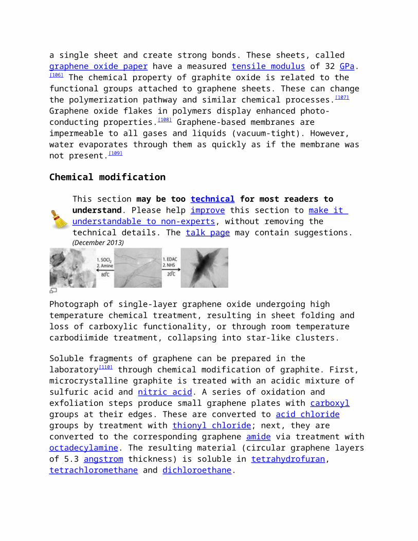
Photograph of single-layer graphene oxide undergoing high temperature chemical treatment, resulting in sheet folding and loss of carboxylic functionality, or through room temperature carbodiimide treatment, collapsing into star-like clusters.

Soluble fragments of graphene can be prepared in the laboratory[110] through chemical modification of graphite. First, microcrystalline graphite is treated with an acidic mixture of sulfuric acid and nitric acid. A series of oxidation and exfoliation steps produce small graphene plates with carboxyl groups at their edges. These are converted to acid chloride groups by treatment with thionyl chloride; next, they are converted to the corresponding graphene amide via treatment with octadecylamine. The resulting material (circular graphene layers of 5.3 angstrom thickness) is soluble in tetrahydrofuran, tetrachloromethane and dichloroethane.
Refluxing single-layer graphene oxide (SLGO) in solvents leads to size reduction and folding of individual sheets as well as loss of carboxylic group functionality, by up to 20%, indicating thermal instabilities of SLGO sheets dependant on their preparation methodology. When using thionyl chloride, acyl chloride groups result, which can then form aliphatic and aromatic amides with a reactivity conversion of around 70–80%.
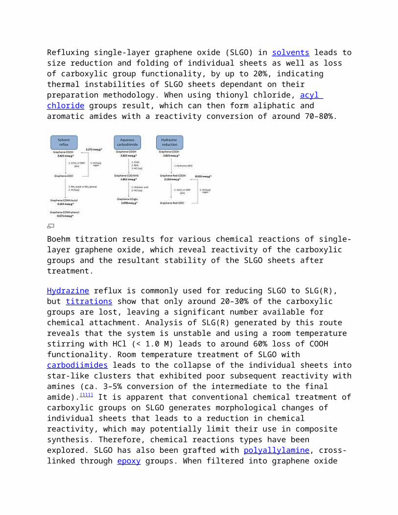
Boehm titration results for various chemical reactions of single-layer graphene oxide, which reveal reactivity of the carboxylic groups and the resultant stability of the SLGO sheets after treatment.
Hydrazine reflux is commonly used for reducing SLGO to SLG(R), but titrations show that only around 20–30% of the carboxylic groups are lost, leaving a significant number available for chemical attachment. Analysis of SLG(R) generated by this route reveals that the system is unstable and using a room temperature stirring with HCl (< 1.0 M) leads to around 60% loss of COOH functionality. Room temperature treatment of SLGO with carbodiimides leads to the collapse of the individual sheets into star-like clusters that exhibited poor subsequent reactivity with amines (ca. 3–5% conversion of the intermediate to the final amide).[111] It is apparent that conventional chemical treatment of carboxylic groups on SLGO generates morphological changes of individual sheets that leads to a reduction in chemical reactivity, which may potentially limit their use in composite synthesis. Therefore, chemical reactions types have been explored. SLGO has also been grafted with polyallylamine, cross-linked through epoxy groups. When filtered into graphene oxide paper, these composites exhibit increased stiffness and strength relative to unmodified graphene oxide paper.[112]
Full hydrogenation from both sides of graphene sheet results in graphane, but partial hydrogenation leads to hydrogenated graphene.[113] Similarly, both-side fluorination of graphene (or chemical and mechanical exfoliation of graphite fluoride) leads to fluorographene (graphene
fluoride), while partial fluorination (generally halogenation) provides fluorinated (halogenated) graphene.
Casimir effect and dispersion
The Casimir effect is an interaction between any disjoint neutral bodies provoked by the fluctuations of the electrodynamical vacuum. Mathematically it can be explained by considering the normal modes of electromagnetic fields, which explicitly depend on the boundary (or matching) conditions on the surfaces of the interacting bodies. Since the interaction of graphene with an electromagnetic field is surprisingly strong for a one-atom-thick material, the Casimir effect is of growing interest.[114][115]
The related van der Waals force (or dispersion force) is also unusual, obeying an inverse cubic, asymptotic power law in contrast to the usual inverse quartic.[116]
Bilayer graphene
Main article: Bilayer graphene
Bilayer graphene displays the anomalous quantum Hall effect, a tunable band gap [117] and potential for excitonic condensation [118] –making them promising candidates for optoelectronic and nanoelectronic applications. Bilayer graphene typically can be found either in twisted configurations where the two layers are rotated relative to each other or graphitic Bernal stacked configurations where half the atoms in one layer lie atop half the atoms in the other. Stacking order and orientation govern the optical and electronic properties of bilayer graphene.
One way to synthesize bilayer graphene is via chemical vapor deposition, and can produce large bilayer regions that almost exclusively conform to a Bernal stack geometry.[119]
3D graphene
In 2013, a three-dimensional honeycomb of hexagonally arranged carbon was termed 3D graphene.[120]
Production techniques
True isolated 2D crystals cannot be grown via chemical synthesis beyond small sizes even in principle. However, other routes to 2d materials exist:
Fundamental forces place seemingly insurmountable barriers in the way of creating [2D crystals]... The nascent 2D crystallites try to minimize their surface energy and inevitably morph into one of the rich variety of stable 3D structures that occur in soot.
But there is a way around the problem. Interactions with 3D structures stabilize 2D crystals during growth. So one can make 2D crystals sandwiched between or placed on top of the atomic
planes of a bulk crystal. In that respect, graphene already exists within graphite... One can then hope to fool Nature and extract single-atom-thick crystallites at a low enough temperature that they remain in the quenched state prescribed by the original higher-temperature 3D growth.[121]
Graphene planes become better separated in intercalated graphite compounds.
Graphene fragments are produced (along with other debris) whenever graphite is abraded, such as when drawing with a pencil.[30]
In 2011 the Institute of Electronic Materials Technology and Department of Physics at Warsaw University announced Sic-baswed epitaxy technology for producing large pieces of graphene with the best quality to date.[122]
Exfoliation
This involves splitting single layers of graphene from multi-layered graphite. Achieving single layers typically requires multiple exfoliation steps, each producing a slice with fewer layers, until only one remains. Geim and Novosolev used adhesive tape to split the layers.
After exfoliation the flakes are deposited on a silicon wafer using "dry deposition". Individual atomic planes can be viewed with an optical microscope. Crystallites larger than 1 mm and visible to the naked eye can be obtained with the technique. It is often referred to as a "scotch tape" or "drawing" method. The latter name appeared because the dry deposition resembles drawing with a piece of graphite.[121]
Single-oriented monolayers of graphene containing bilayer regions can be formed on silicon carbide crystal surfaces and transferred to other substrates. A nickel film grown to a thickness designed to impart a particular surface stress acts as a “handle” for moving the graphene to a silica substrate. An additional gold layer can remove any excess layers to create a monolayer suitable for electronics applications.[123][124]
Free-standing atomic planes of boron nitride, mica, dichalcogenides and complex oxides can also be obtained using the drawing method.[125] These 2D materials have so far attracted little attention.
Epitaxy
Epitaxy refers to the deposition of a crystalline overlayer on a crystalline substrate, where there is registry between the two. In some cases epitaxial graphene layers are coupled to surfaces weakly enough (by Van der Waals forces) to retain the two dimensional electronic band structure of isolated graphene.[126][127] An example of weakly coupled epitaxial graphene is the one grown on SiC.[32]
Graphene monolayers grown on SiC and Ir are weakly coupled to these substrates (how weakly remains debated) and the graphene–substrate interaction can be further passivated.[13]
Silicon carbide
Main article: Carbide-derived Carbon
Heating silicon carbide (SiC) to high temperatures (>1,100 °C) under low pressures (~10−6 torr) reduces it to graphene.[128] This process produces epitaxial graphene with dimensions dependent upon the size of the wafer. The face of the SiC used for graphene formation, silicon- or carbon-terminated, highly influences the thickness, mobility and carrier density of the resulting graphene.
The electronic band-structure (so-called Dirac cone structure) was first visualized in this material.[129][130][131] Weak anti-localization is observed in this material, but not in exfoliated graphene produced by the pencil-trace method.[132] Large, temperature-independent mobilities have been observed, approaching those in exfoliated graphene placed on silicon oxide, but lower than mobilities in suspended graphene produced by the drawing method. Even without transfer, graphene on SiC exhibits massless Dirac fermions.[95][96][97][98][99][100]
The weak van der Waals force that provides the cohesion of multilayer graphene stacks does not always affect the electronic properties of the individual graphene layers in the stack. That is, while the electronic properties of certain multilayered epitaxial graphenes are identical to that of a single layer,[133] in other cases the properties are affected,[129][130] as they are in bulk graphite. This effect is well understood theoretically and is related to the symmetry of the interlayer interactions.[133]
Epitaxial graphene on SiC can be patterned using standard microelectronics methods. The band gap can be tuned by laser irradiation.[134]
Metal substrates
The atomic structure of a metal substrate can seed the growth of graphene. Graphene grown on ruthenium does not typically produce uniform layer thickness. Bonding between the bottom graphene layer and the substrate may affect layer properties.[135]
Graphene grown on iridium is very weakly bonded, uniform in thickness and can be highly ordered. As on many other substrates, graphene on iridium is slightly rippled. Due to the long-range order of these ripples, minigaps in the electronic band-structure (Dirac cone) become visible.[136] High-quality sheets of few-layer graphene exceeding 1 cm2 (0.2 sq in) in area have been synthesized via chemical vapor deposition on thin nickel films with methane as a carbon source. These sheets have been successfully transferred to various substrates.[137][95][138]
An improvement of this technique employs copper foil; at very low pressure, the growth of graphene automatically stops after a single graphene layer forms. Arbitrarily large films can be created.[137][139] The single layer growth is also due to low concentration of carbon in methane. Larger hydrocarbons such as ethane and propane produce bilayer graphene.[140] Atmospheric pressure CVD growth produces multilayer graphene on copper (similar to that grown on nickel
films).[141] Graphene has been demonstrated at temperatures compatible with conventional CMOS processing, using a nickel-based alloy with gold as catalyst.[142]
Reduction
Graphite oxide reduction was probably the first method of graphene synthesis. P. Boehm reported producing monolayer flakes of reduced graphene oxide in 1962.[143] Geim acknowledged Boehm's contribution.[144] Rapid heating of graphite oxide and exfoliation yields highly dispersed carbon powder with a few percent of graphene flakes. Reduction of graphite oxide monolayer films, e.g. by hydrazine, annealing in argon/hydrogen, was reported to yield graphene films. However, the quality is lower compared to scotch-tape graphene, due to incomplete removal of functional groups. Furthermore, the oxidation protocol introduces permanent defects due to over-oxidation. Recently, the oxidation protocol was enhanced to yield graphene oxide with an almost intact carbon framework that allows highly efficient removal of functional groups. The measured charge carrier mobility exceeded 1,000 centimetres (393.70 in)/Vs.[145] Spectroscopic analysis of reduced graphene oxide has been conducted.[146][147]
Applying a layer of graphite oxide film to a DVD and burning it in a DVD writer produced a thin graphene film with high electrical conductivity (1738 siemens per meter) and specific surface area (1520 square meters per gram), and was highly resistant and malleable.[148]
Metal-carbon melts
This process dissolves carbon atoms inside a transition metal melt at a certain temperature and then precipitates the dissolved carbon at lower temperatures as single layer graphene (SLG).[149]
The metal is first melted in contact with a carbon source, possibly a graphite crucible inside which the melt is carried out or graphite powder or chunks that are placed in the melt. Keeping the melt in contact with the carbon at a specific temperature dissolves the carbon atoms, saturating the melt based on the binary phase diagram of metal-carbon. Upon lowering the temperature, carbon's solubility decreases and the excess carbon precipitates atop the melt. The floating layer can be either skimmed or frozen for later removal. Using different morphology, including thick graphite, few layer graphene (FLG) and SLG were observed on metal substrate. Raman spectroscopy proved that SLG had grown on nickel substrate. The SLG Raman spectrum featured no D and D′ band, indicating its pristine nature. Among transition metals, nickel provides the best substrate for growing SLG. Since nickel is not Raman active, direct Raman spectroscopy of graphene layers on top of the nickel is achievable.[149]
Sodium ethoxide pyrolysis
Gram-quantities of graphene were produced by the reduction of ethanol by sodium metal, followed by pyrolysis of the ethoxide product and washing with water to remove sodium salts.[150]
Nanotube slicing
Graphene can be created by cutting open carbon nanotubes.[151] In one such method multi-walled carbon nanotubes are cut open in solution by action of potassium permanganate and sulfuric acid.[152] In another method graphene nanoribbons were produced by plasma etching of nanotubes partly embedded in a polymer film.[153]
Graphite sonication
Dispersing graphite in a proper liquid medium can be produce graphene by sonication. Non-exfoliated graphite is separated from graphene by centrifugation,[154] producing graphene concentrations initially up to 0.01 mg/ml in N-methylpyrrolidone (NMP) and later to 2.1 mg/ml in NMP,.[155] Using a suitable ionic liquid as the dispersing liquid medium for graphite exfoliation[156] produced concentrations of 5.33 mg/ml.
Carbon dioxide reduction
A highly exothermic reaction combusts magnesium in an oxidation-reduction reaction with carbon dioxide, producing a variety of carbon nanoparticles including graphene and fullerenes. The carbon dioxide reactant may be either solid (dry-ice) or gaseous. The products of this reaction are carbon and magnesium oxide. US patent 8377408 was issued for this process.[157]
Potential applications
Potential applications include lightweight, thin, flexible, yet durable display screens, electric circuits, and solar cells, as well as various medical, chemical and industrial processes enhanced or enabled by the use of new graphene materials.[158]
In 2008, graphene produced by exfoliation was one of the most expensive materials on Earth, with a sample with the area of the cross section of a human hair costing more than $1,000 as of April 2008 (about $100,000,000/cm2).[30] Since then, exfoliation procedures have been scaled up, and now companies sell graphene in large quantities.[159] The price of epitaxial graphene on SiC is dominated by the substrate price, which was approximately $100/cm2 as of 2009.
This article is outdated. Please update this article to reflect recent events or newly available information. (December 2013)
Hong and his team in South Korea pioneered the synthesis of large-scale graphene films using chemical vapour deposition (CVD) on thin nickel layers, which triggered research on practical applications,[160] with wafer sizes up to 30 inches (760 mm) reported.[137]
In 2013, the European Union made a €1 billion grant to be used for research into potential graphene applications.[161] In 2013 the Graphene Flagship consortium formed, including Chalmers University of Technology and seven other European universities and research centers, along with Nokia.[162] Nokia has also been working on graphene technology for several years.[163]
Medicine
Graphene is reported to have enhanced PCR by increasing the yield of DNA product.[164] Experiments revealed that graphene's thermal conductivity could be the main factor behind this result. Graphene yields DNA product equivalent to positive control with up to 65% reduction in PCR cycles.
Integrated circuits
For integrated circuits, graphene has a high carrier mobility, as well as low noise, allowing it to be used as the channel in a field-effect transistor. Single sheets of graphene are hard to produce and even harder to make on an appropriate substrate.[165]
In 2008, the smallest transistor so far, one atom thick, 10 atoms wide was made of graphene.[166] IBM announced in December 2008 that they had fabricated and characterized graphene transistors operating at GHz frequencies.[167] In May 2009, an n-type transistor was announced meaning that both n and p-type graphene transistors had been created.[168][169] A functional graphene integrated circuit was demonstrated – a complementary inverter consisting of one p- and one n-type graphene transistor.[170] However, this inverter suffered from a very low voltage gain.
According to a January 2010 report,[171] graphene was epitaxially grown on SiC in a quantity and with quality suitable for mass production of integrated circuits. At high temperatures, the quantum Hall effect could be measured in these samples. IBM built 'processors' using 100 GHz transistors on 2-inch (51 mm) graphene sheets.[172]
In June 2011, IBM researchers announced that they had succeeded in creating the first graphene-based integrated circuit, a broadband radio mixer.[173] The circuit handled frequencies up to 10 GHz. Its performance was unaffected by temperatures up to 127 C.
In June 2013 an 8 transistor 1.28 GHz ring oscillator circuit was described.[174]
Transistors
Graphene exhibits a pronounced response to perpendicular external electric fields, potentially forming field-effect transistors (FET). A 2004 paper documented FETs with an on-off ratio of ~30 at room temperature.[citation needed] A 2006 paper announced an all-graphene planar FET with side gates.[175] Their devices showed changes of 2% at cryogenic temperatures. The first top-gated FET (on–off ratio of <2) was demonstrated in 2007.[176] Graphene nanoribbons may prove generally capable of replacing silicon as a semiconductor.[177]
US patent 7015142 for graphene-based electronics was issued in 2006. In 2008, researchers at MIT Lincoln Lab produced hundreds of transistors on a single chip[178] and in 2009, very high frequency transistors were produced at Hughes Research Laboratories.[179]
A 2008 paper demonstrated a switching effect based on a reversible chemical modification of the graphene layer that gives an on–off ratio of greater than six orders of magnitude. These reversible switches could potentially be employed in nonvolatile memories.[180]
In 2009, researchers demonstrated four different types of logic gates, each composed of a single graphene transistor.[181]
Practical uses for these circuits are limited by the very small voltage gain they exhibit. Typically, the amplitude of the output signal is about 40 times less than that of the input signal. Moreover, none of these circuits operated at frequencies higher than 25 kHz.
In the same year, tight-binding numerical simulations[182] demonstrated that the band-gap induced in graphene bilayer field effect transistors is not sufficiently large for high-performance transistors for digital applications, but can be sufficient for ultra-low voltage applications, when exploiting a tunnel-FET architecture.[183]
In February 2010, researchers announced transistors with an on/off rate of 100 gigahertz, far exceeding the rates of previous attempts, and exceeding the speed of silicon transistors with an equal gate length. The 240 nm devices were made with conventional silicon-manufacturing equipment.[184][185][186]
In November 2011, researchers used 3d printing (additive manufacturing) as a method for fabricating graphene devices.[187]
In 2013, researchers demonstrated graphene's high mobility in a detector that allows broad band frequency selectivity ranging from the THz to IR region (0.76-33THz)[188] A separate group created a terahertz-speed transistor with bistable characteristics, which means that the device can spontaneously switch between two electronic states. The device consists of two layers of graphene separated by an insulating layer of boron nitride a few atomic layers thick. Electrons move through this barrier by quantum tunneling. These new transistors exhibit “negative differential conductance,” whereby the same electrical current flows at two different applied voltages.[189]
Graphene does not have an energy band-gap, which presents a hurdle for its applications in digital logic gates. The efforts to induce a band-gap in graphene via quantum confinement or surface functionalization have not resulted in a breakthrough. The negative differential resistance experimentally observed in graphene field-effect transistors of "conventional" design allows for construction of viable non-Boolean computational architectures with the gap-less graphene. The negative differential resistance - observed under certain biasing schemes - is an intrinsic property of graphene resulting from its symmetric band structure. The results present a conceptual change in graphene research and indicate an alternative route for graphene's applications in information processing.[190]
In 2013 researchers reported the creation of transistors printed on flexible plastic that operate at 25-gigahertz, sufficient for communications circuits and that can be fabricated at scale. The researchers first fabricate the non-graphene-containing structures—the electrodes and gates—on plastic sheets. Separately, they grow large graphene sheets on metal, then peel it off and transfer it to the plastic. Finally, they top the sheet with a waterproof layer. The devices work after being soaked in water, and are flexible enough to be folded.[191]

Redox
Graphene oxide can be reversibly reduced and oxidized using electrical stimulus. Controlled reduction and oxidation in two-terminal devices containing multilayer graphene oxide films are shown to result in switching between partially reduced graphene oxide and graphene, a process that modifies the electronic and optical properties. Oxidation and reduction are related to resistive switching.[192]
Transparent conducting electrodes
Graphene's high electrical conductivity and high optical transparency make it a candidate for transparent conducting electrodes, required for such applications as touchscreens, liquid crystal displays, organic photovoltaic cells, and organic light-emitting diodes. In particular, graphene's mechanical strength and flexibility are advantageous compared to indium tin oxide, which is brittle. Graphene films may be deposited from solution over large areas.[193][194]
Large-area, continuous, transparent and highly conducting few-layered graphene films were produced by chemical vapor deposition and used as anodes for application in photovoltaic devices. A power conversion efficiency (PCE) up to 1.71% was demonstrated, which is 55.2% of the PCE of a control device based on indium tin oxide.[195]
Organic light-emitting diodes (OLEDs) with graphene anodes have been demonstrated.[196] The electronic and optical performance of graphene-based devices are similar to devices made with indium tin oxide.
A carbon-based device called a light-emitting electrochemical cell (LEC) was demonstrated with chemically-derived graphene as the cathode and the conductive polymer PEDOT as the anode.[197] Unlike its predecessors, this device contains only carbon-based electrodes, with no metal.
Ethanol distillation
Graphene oxide membranes allow water vapor to pass through, but are impermeable to other liquids and gases.[109] This phenomenon has been used for further distilling of vodka to higher alcohol concentrations, in a room-temperature laboratory, without the application of heat or vacuum as used in traditional distillation methods.[198] Further development and commercialization of such membranes could revolutionize the economics of biofuel production and the alcoholic beverage industry.
Desalination
Research suggests that graphene filters could outperform other techniques of desalination by a significant margin.[199]
Solar cells

Graphene has a unique combination of high electrical conductivity and optical transparency, which make it a candidate for use in solar cells. A single sheet of graphene is a zero-bandgap semiconductor whose charge carriers are delocalized over large areas, implying that carrier scattering does not occur. Because this material only absorbs 2.3% of visible light, it is a candidate for applications requiring a transparent conductor. Graphene can be assembled into a film electrode with low roughness. However, graphene films produced via solution processing contain lattice defects and grain boundaries that act as recombination centers and decrease the material's electrical conductivity. Thus, these films must be made thicker than one atomic layer to obtain useful sheet resistances. This added resistance can be combatted by incorporating conductive filler materials, such as a silica matrix. Reduced graphene film's electrical conductivity can be improved by attaching large aromatic molecules such as pyrene-1-sulfonic acid sodium salt (PyS) and the disodium salt of 3,4,9,10-perylenetetracarboxylic diimide bisbenzenesulfonic acid (PDI). These large aromatic molecules, under high temperatures, facilitate better π-conjugation of the graphene basal plane. Graphene films have high transparency in the visible and near-infrared regions and are chemically and thermally stable.[200]
For graphene to be used in commercial solar cells, large-scale production are required. However, the peeling of pyrolytic graphene is not yet a scalable process. An alternative potentially scalable process is thermal decomposition of silicon carbide.[200]
Graphene's high charge mobilities recommend if for use as a charge collector and transporter in photovoltaics. Using graphene as a photoactive material requires its bandgap to be 1.4-1.9eV. In 2010, single cell efficiencies of nanostructured graphene-based PVs of over 12% were achieved. According to P. Mukhopadhyay and R. K. Gupta OPVs could be "devices in which semiconducting graphene is used as the photoactive material and metallic graphene is used as the conductive electrodes".[200]
Large scale production of highly transparent graphene films by chemical vapor deposition was achieved in 2008. In this process, ultra-thin graphene sheets are created by first depositing carbon atoms in the form of graphene films on a nickel plate from methane gas. A protective layer of thermoplastic is laid over the graphene layer and the nickel underneath is dissolved in an acid bath. The final step is to attach the plastic-protected graphene to a flexible polymer sheet, which can then be incorporated into an OPV cell. Graphene/polymer sheets range in size up to 150 square centimeters and can be used to create dense arrays of flexible OPV cells. It may eventually be possible to run printing presses covering extensive areas with inexpensive solar cells, much like newspaper presses print newspapers (roll-to-roll).[201]
Silicon generates only one current-driving electron for each photon it absorbs, while graphene can produce multiple electrons. Solar cells made with graphene could offer 60% conversion efficiency – double the widely-accepted maximum efficiency of silicon cells.[202]
Single-molecule gas detection
Theoretically graphene makes an excellent sensor due to its 2D structure. The fact that its entire volume is exposed to its surrounding makes it very efficient to detect adsorbed molecules. However, similar to carbon nanotubes, graphene has no dangling bonds on its surface. Gaseous

molecules cannot be readily adsorbed onto graphene surfaces, so intrinsically graphene is insensitive.[203] The sensitivity of graphene chemical gas sensors can be dramatically enhanced by functionalization, for example, coating the film with a thin layer of certain polymers. The thin polymer layer acts like a concentrator that absorbs gaseous molecules. The molecule absorption introduces a local change in electrical resistance of graphene sensors. While this effect occurs in other materials, graphene is superior due to its high electrical conductivity (even when few carriers are present) and low noise, which makes this change in resistance detectable.[54]
Quantum dots
Graphene quantum dots (GQDs) keep all dimensions less than 10 nm. Their size and edge crystallography govern their electrical, magnetic, optical and chemical properties. GQDs can be produced via graphite nanotomy[204] or via bottom-up, solution-based routes (Diels-Alder, cyclotrimerization and/or cyclodehydrogenation reactions).[205] GQDs with controlled structure can be incorporated into applications in electronics, optoelectronics and electromagnetics. Quantum confinement can be created by changing the width of GNRs[clarification needed] at select points along the ribbon.[166][206]
Frequency multiplier
In 2009, researchers built experimental graphene frequency multipliers that take an incoming signal of a certain frequency and output a signal at a multiple of that frequency.[207]
Optical modulator
When the Fermi level of graphene is tuned, its optical absorption can be changed. In 2011, researchers reported the first graphene-based optical modulator. Operating at 1.2 GHz without a temperature controller, this modulator has a broad bandwidth (from 1.3 to 1.6 μm) and small footprint (~25 μm2).[208]
Coolant additive
Graphene's high thermal conductivity suggests that it could be used as an additive in coolants. Preliminary research work showed that 5% graphene by volume can enhance the thermal conductivity of a base fluid by 86%.[209] Another application due to graphene's enhanced thermal conductivity was found in PCR.[210]
Reference material
Graphene's properties suggest it as a reference material for characterizing electroconductive and transparent materials. One layer of graphene absorbs 2.3% of white light.[211]
This property was used to define the conductivity of transparency that combines sheet resistance and transparency. This parameter was used to compare materials without the use of two independent parameters.[212]

Thermal management
In 2011, researchers reported that a three-dimensional, vertically aligned, functionalized multilayer graphene architecture can be an approach for graphene-based thermal interfacial materials (TIMs) with superior thermal conductivity and ultra-low interfacial thermal resistance between graphene and metal.[80]
Graphene-metal composites can be utilized in thermal interface materials.[149]
Energy storage
Supercapacitor
Due to graphene's high surface area to mass ratio, one potential application is in the conductive plates of supercapacitors.[213]
In February 2013 researchers announced a novel technique to produce graphene supercapacitors based on the DVD burner reduction approach.[214]
Electrode for Li-ion batteries
Stable Li-ion cycling has recently been demonstrated in bi- and few layer graphene films grown on nickel substrates,[215] while single layer graphene films have been demonstrated as a protective layer against corrosion in battery components such as the battery case.[216] This creates possibilities for flexible electrodes for microscale Li-ion batteries where the anode acts as the active material as well as the current collector.[217]
Engineered piezoelectricity
Density functional theory simulations predict that depositing certain adatoms on graphene can render it piezoelectrically responsive to an electric field applied in the out-of-plane direction. This type of locally engineered piezoelectricity is similar in magnitude to that of bulk piezoelectric materials and makes graphene a candidate for control and sensing in nanoscale devices.[218]
Biodevice
Graphene's modifiable chemistry, large surface area, atomic thickness and molecularly gatable structure make antibody-functionalized graphene sheets excellent candidates for mammalian and microbial detection and diagnosis devices.[219]

Energy of the electrons with wavenumber k in graphene, calculated in the Tight Binding-approximation. The unoccupied (occupied) states, colored in blue–red (yellow–green), touch each other without energy gap exactly at the above-mentioned six k-vectors.
The most ambitious biological application of graphene is for rapid, inexpensive electronic DNA sequencing. Integration of graphene (thickness of 0.34 nm) layers as nanoelectrodes into a nanopore[220] can solve a bottleneck for nanopore-based single-molecule DNA sequencing.
On November 20, 2013 the Bill & Melinda Gates Foundation awarded $100,000 to 'to develop new elastic composite materials for condoms containing nanomaterials like graphene'.[221]
Pseudo-relativistic theory
Graphene's electrical properties can be described by a conventional tight-binding model; in this model the energy of the electrons with wave vector k is[222][47]
with the nearest-neighbor hopping energy γ0 ≈ 2.8 eV and the lattice constant a ≈ 2.46 Å. The conduction and valence band, respectively, correspond to the different signs in the above dispersion relation; they touch each other at six points, the "K-values". However, only two of these six points are independent, while the rest are equivalent by symmetry. In the vicinity of the K-points the energy depends linearly on the wave vector, similar to a relativistic particle. Since an elementary cell of the lattice has a basis of two atoms, the wave function even has an effective 2-spinor structure.

As a consequence, at low energies, even neglecting the true spin, the electrons can be described by an equation that is formally equivalent to the massless Dirac equation. This pseudo-relativistic description is restricted to the chiral limit, i.e., to vanishing rest mass M0, which leads to interesting additional features:[47][223]
Here vF ~ 106 is the Fermi velocity in graphene, which replaces the velocity of light in the Dirac
theory; is the vector of the Pauli matrices, is the two-component wave function of the electrons, and E is their energy.[105]
Related Documents