LC OSCILLATOR CHIRP GENERATOR FOR LADAR APPLICATIONS Joseph Grace III MSEE Defense April 19th, 2013 Advisory Committee: Nuri Emanetoglu, Assistant Professor of Electrical and Computer Engineering, Advisor Donald Hummels, Professor and Chair of Electrical and Computer Engineering David Kotecki, Associate Professor of Electrical and Computer Engineering

Welcome message from author
This document is posted to help you gain knowledge. Please leave a comment to let me know what you think about it! Share it to your friends and learn new things together.
Transcript
LC OSCILLATOR CHIRP GENERATOR
FOR LADAR APPLICATIONS
Joseph Grace III
MSEE Defense
April 19th, 2013
Advisory Committee:
Nuri Emanetoglu, Assistant Professor of Electrical and Computer Engineering, Advisor
Donald Hummels, Professor and Chair of Electrical and Computer Engineering
David Kotecki, Associate Professor of Electrical and Computer Engineering
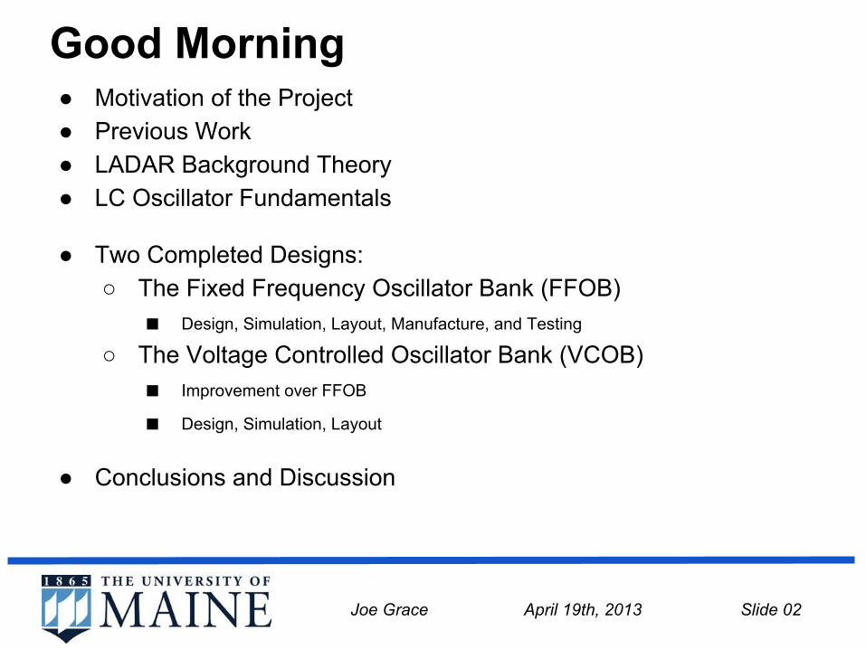
Good Morning● Motivation of the Project● Previous Work● LADAR Background Theory● LC Oscillator Fundamentals
● Two Completed Designs:○ The Fixed Frequency Oscillator Bank (FFOB)
■ Design, Simulation, Layout, Manufacture, and Testing
○ The Voltage Controlled Oscillator Bank (VCOB)■ Improvement over FFOB
■ Design, Simulation, Layout
● Conclusions and Discussion
Joe Grace April 19th, 2013 Slide 02
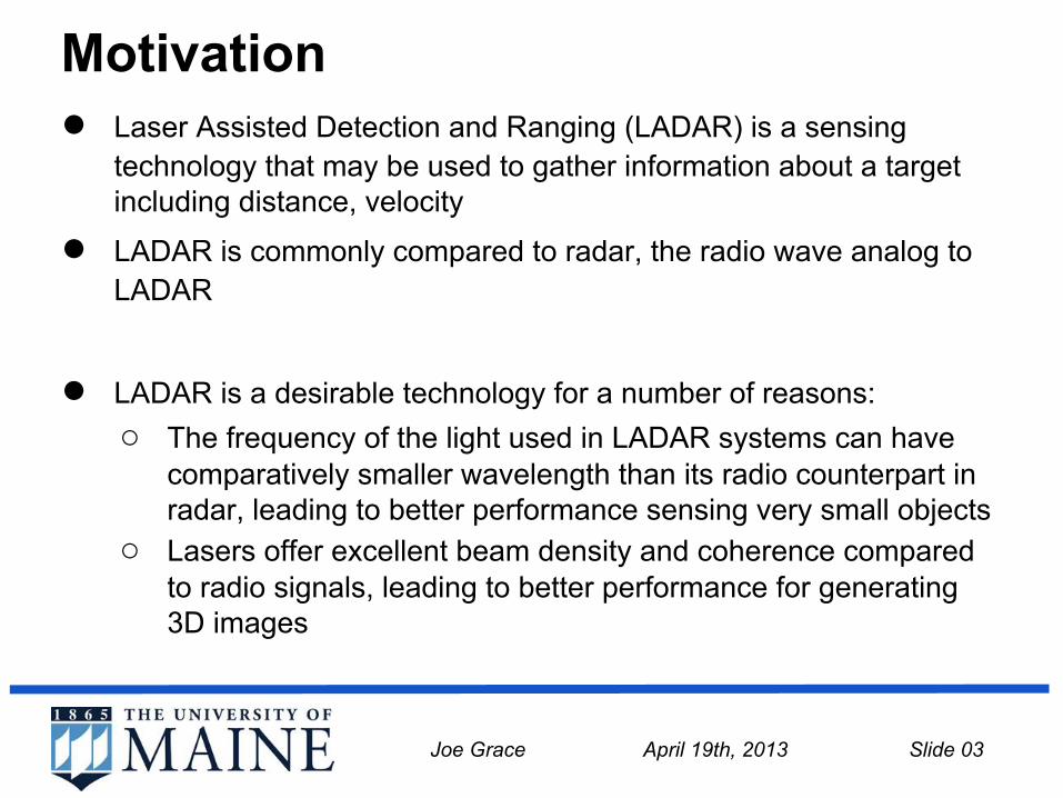
Motivation ● Laser Assisted Detection and Ranging (LADAR) is a sensing
technology that may be used to gather information about a target including distance, velocity
● LADAR is commonly compared to radar, the radio wave analog to LADAR
● LADAR is a desirable technology for a number of reasons:○ The frequency of the light used in LADAR systems can have
comparatively smaller wavelength than its radio counterpart in radar, leading to better performance sensing very small objects
○ Lasers offer excellent beam density and coherence compared to radio signals, leading to better performance for generating 3D images
Joe Grace April 19th, 2013 Slide 03

Motivation ● LADAR applications include:
○ Collision avoidance○ Target recognition and range finding○ Terrain Mapping
● LADAR systems may be improved and applied to a wider array of applications if they can be miniaturized
● The goal of this project was to take a crucial part of a LADAR system, the "chirp" signal generator, and put it on a CMOS IC
● One step along path to a complete LADAR system-on-a-chip
Joe Grace April 19th, 2013 Slide 04
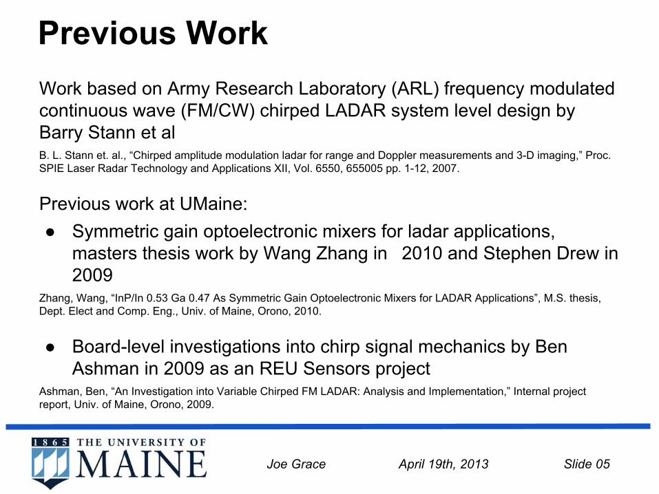
Previous WorkWork based on Army Research Laboratory (ARL) frequency modulated continuous wave (FM/CW) chirped LADAR system level design by Barry Stann et alB. L. Stann et. al., “Chirped amplitude modulation ladar for range and Doppler measurements and 3-D imaging,” Proc. SPIE Laser Radar Technology and Applications XII, Vol. 6550, 655005 pp. 1-12, 2007.
Previous work at UMaine:● Symmetric gain optoelectronic mixers for ladar applications,
masters thesis work by Wang Zhang in 2010 and Stephen Drew in 2009
Zhang, Wang, “InP/In 0.53 Ga 0.47 As Symmetric Gain Optoelectronic Mixers for LADAR Applications”, M.S. thesis, Dept. Elect and Comp. Eng., Univ. of Maine, Orono, 2010.
● Board-level investigations into chirp signal mechanics by Ben Ashman in 2009 as an REU Sensors project
Ashman, Ben, “An Investigation into Variable Chirped FM LADAR: Analysis and Implementation,” Internal project report, Univ. of Maine, Orono, 2009.
Joe Grace April 19th, 2013 Slide 05
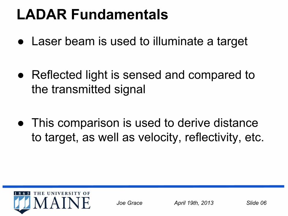
LADAR Fundamentals
● Laser beam is used to illuminate a target
● Reflected light is sensed and compared to the transmitted signal
● This comparison is used to derive distance to target, as well as velocity, reflectivity, etc.
Joe Grace April 19th, 2013 Slide 06
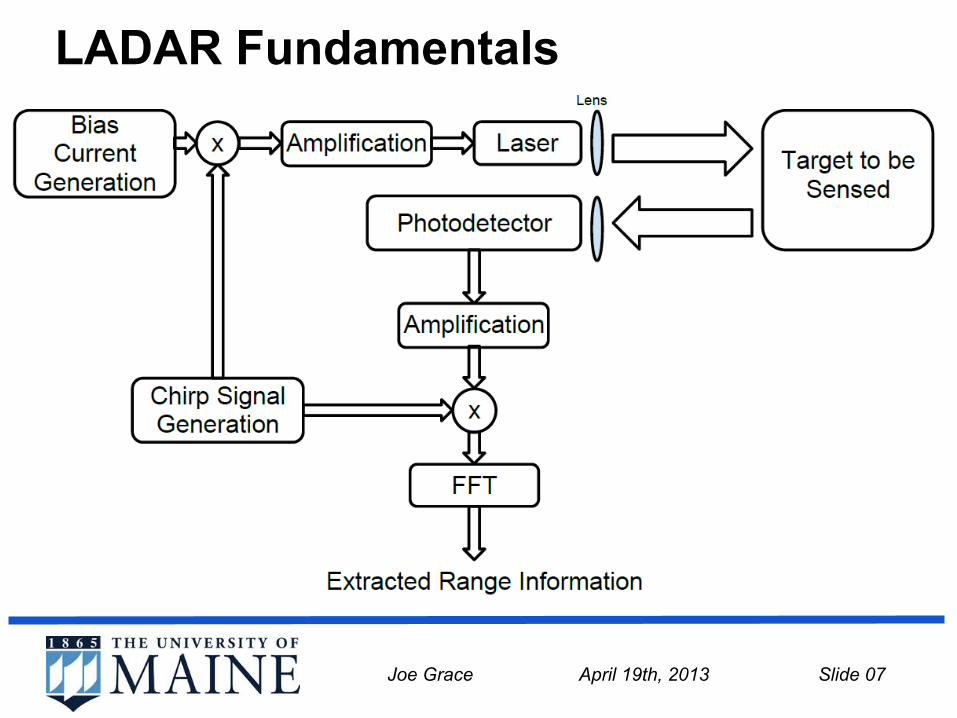
LADAR Fundamentals
Joe Grace April 19th, 2013 Slide 07
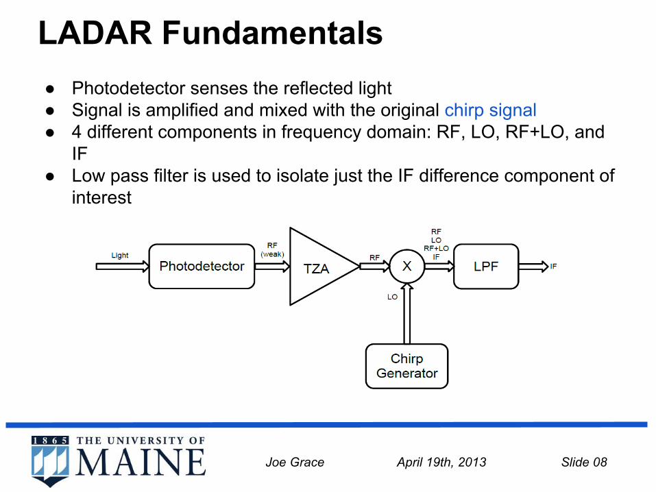
LADAR Fundamentals● Photodetector senses the reflected light● Signal is amplified and mixed with the original chirp signal● 4 different components in frequency domain: RF, LO, RF+LO, and
IF● Low pass filter is used to isolate just the IF difference component of
interest
Joe Grace April 19th, 2013 Slide 08
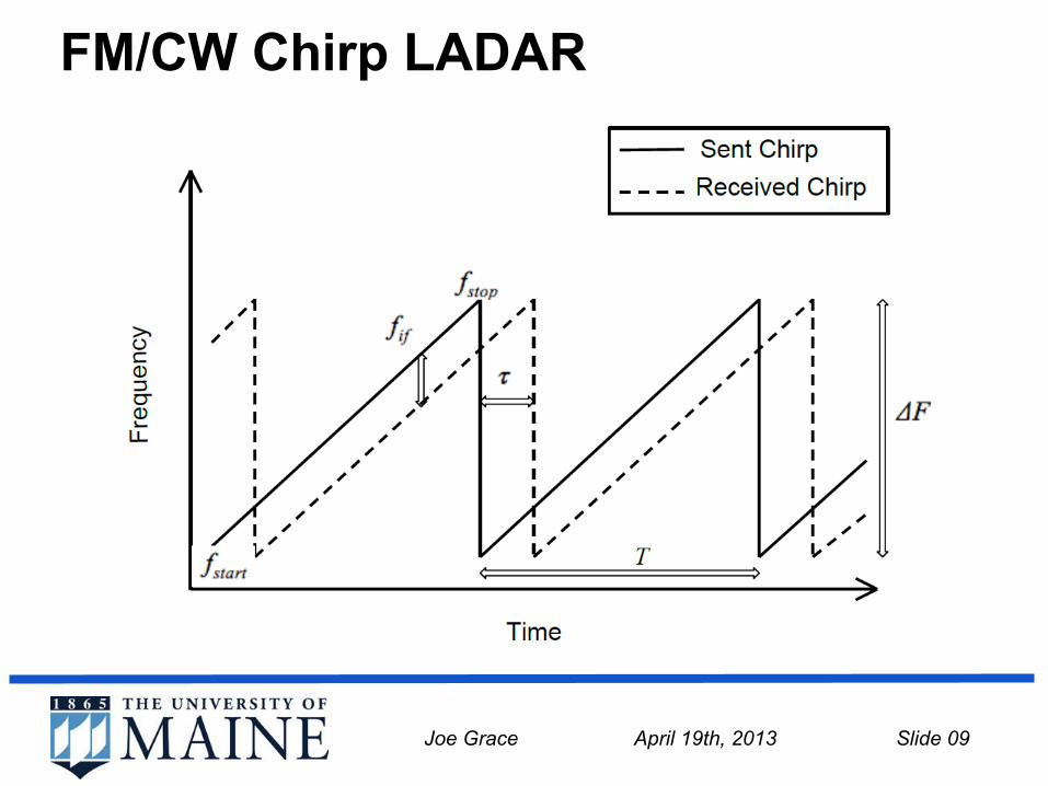
FM/CW Chirp LADAR
Joe Grace April 19th, 2013 Slide 09

FM/CW Chirp LADARThe difference in frequency is proportional to the time delay between the transmitted and reflected signals:
This represents the fundamental relationship that makes both FM/CW radar and LADAR possible.
The time delay expressed in terms of the distance to the target, D:
Combining these equations yields
which relates the intermediate frequency to the metric of interest, D.
Joe Grace April 19th, 2013 Slide 10
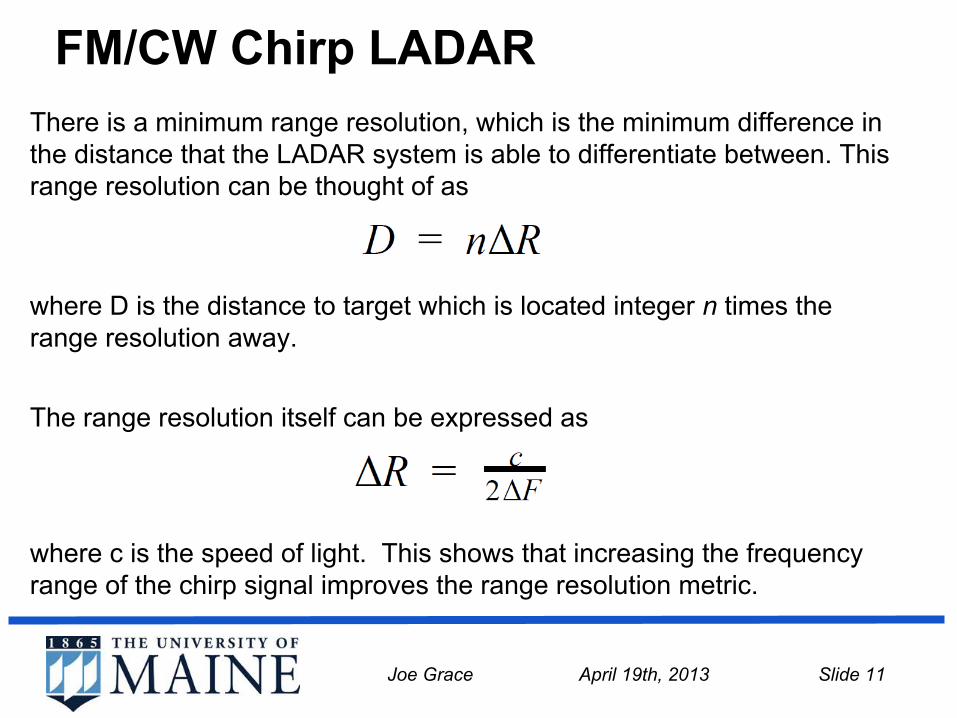
FM/CW Chirp LADARThere is a minimum range resolution, which is the minimum difference in the distance that the LADAR system is able to differentiate between. This range resolution can be thought of as
where D is the distance to target which is located integer n times the range resolution away.
The range resolution itself can be expressed as
where c is the speed of light. This shows that increasing the frequency range of the chirp signal improves the range resolution metric.
Joe Grace April 19th, 2013 Slide 11
LC Oscillator Fundamentals
Joe Grace April 19th, 2013 Slide 12
That concludes the background theory on LADAR systems.
Next topic is....
LC Oscillator Fundamentals
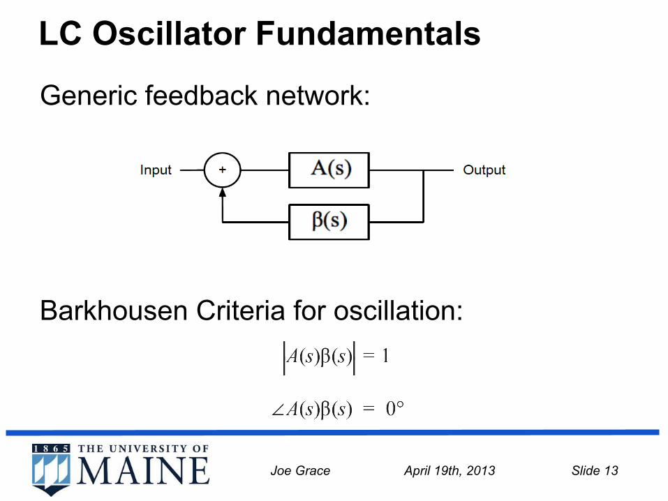
Generic feedback network:
Barkhousen Criteria for oscillation:
Joe Grace April 19th, 2013 Slide 13
LC Oscillator Fundamentals
Joe Grace April 19th, 2013 Slide 14
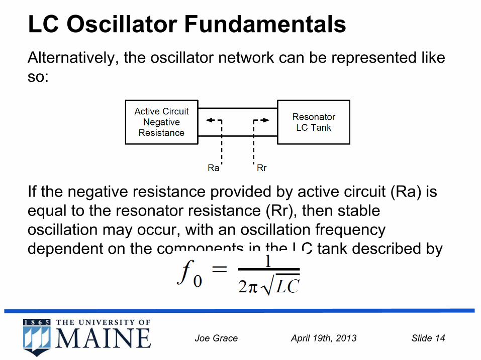
Alternatively, the oscillator network can be represented like so:
If the negative resistance provided by active circuit (Ra) is equal to the resonator resistance (Rr), then stable oscillation may occur, with an oscillation frequency dependent on the components in the LC tank described by

LC Oscillator Fundamentals
Joe Grace April 19th, 2013 Slide 15
Single Transistor LC Oscillators(a) Generic Direct Feedback Oscillator(b) Colpitts Oscillator(c) Hartley Oscillator
Single Transistor LC oscillators utilize the transconductance of a MOSFET to provide the negative resistance to sustain oscillation.
Two most common topologies use a capacitor divider network (Colpitts) or an inductor divider (Hartley) to provide feedback.
These topologies offer only a single ended output and have poor quality factors relative to their required area on chip.

LC Oscillator Fundamentals
Joe Grace April 19th, 2013 Slide 16
Multiple Transistor LC Oscillators(a) NMOS LC Oscillator(b) CMOS LC Oscillator
Multiple transistor oscillators offer a double ended output and do not require capacitor or inductor divider feedback networks, but does require strong device matching.
The transconductance of the NMOS pair provides the negative resistance necessary to sustain oscillation, and the addition of PMOS transistors further improves this transconductance and makes sustaining oscillation easier.
Note that the addition of more transistors represents an acceptable increase in chip space since these components are not significantly sized compared to the LC tank, and only a single LC tank is used.
(a)
(b)

All work was completed in the Cadence Design Environment, utilizing the IBM CMRF7SF process, with manufacture being handled by MOSIS.
Two different designs:- Fixed Frequency Oscillator Bank (FFOB) Design and Simulation - Fall 2011 Layout and Extraction Simulation - Spring 2012 Manufacture and Testing - Summer and Fall 2012
- Voltage Controlled Oscillator Bank (VCOB) Improved design to address FFOB's shortcomings Design and Simulation - Fall 2012 and Spring 2013 Layout - Spring 2013
Scope of Work
Joe Grace April 19th, 2013 Slide 17

The FFOB
Joe Grace April 19th, 2013 Slide 18
Generates 16 discrete frequencies spaced 100 MHz apart ranging from fstart=600 MHz to fstop=2.1 GHz, for a total bandwidth of 1.5 GHz.
Each oscillation frequency is generated by its own fixed LC oscillator. Each oscillator is turned on and off by its own input control pin on the IC package.
3.3V supply and devices were used, with a single output capable of driving a 50 Ohm load with a current swing of 0-30mA

The FFOB - Oscillator Schematic
Joe Grace April 19th, 2013 Slide 19

The FFOB - Oscillator Schematic
Joe Grace April 19th, 2013 Slide 20
The LC Oscillator

The FFOB - Oscillator Schematic
Joe Grace April 19th, 2013 Slide 21
Bias Current Generationand Current Cutoff
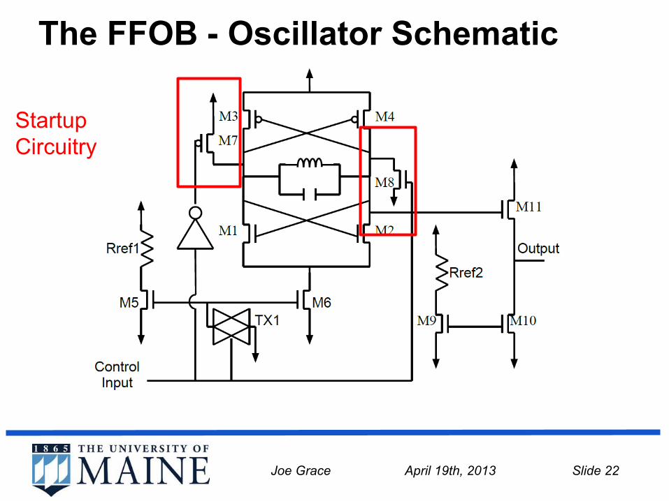
The FFOB - Oscillator Schematic
Joe Grace April 19th, 2013 Slide 22
StartupCircuitry

The FFOB - Oscillator Schematic
Joe Grace April 19th, 2013 Slide 23
Source FollowerOutput Stage
The FFOB
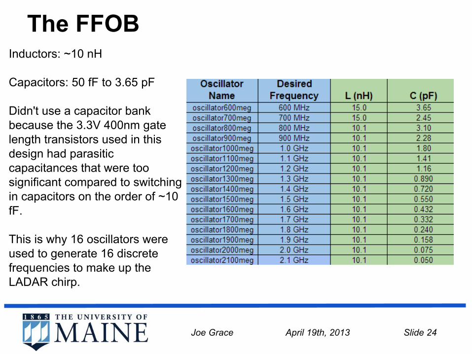
Joe Grace April 19th, 2013 Slide 24
Inductors: ~10 nH
Capacitors: 50 fF to 3.65 pF
Didn't use a capacitor bank because the 3.3V 400nm gate length transistors used in this design had parasitic capacitances that were too significant compared to switching in capacitors on the order of ~10 fF.
This is why 16 oscillators were used to generate 16 discrete frequencies to make up the LADAR chirp.

The FFOB - Oscillator Layout
Joe Grace April 19th, 2013 Slide 25
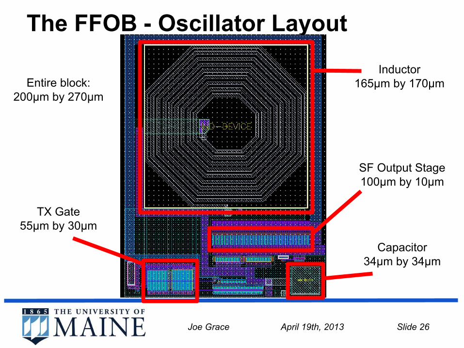
The FFOB - Oscillator Layout
Joe Grace April 19th, 2013 Slide 26
Inductor165μm by 170μm
SF Output Stage100μm by 10μm
Capacitor34μm by 34μm
TX Gate55μm by 30μm
Entire block:200μm by 270μm
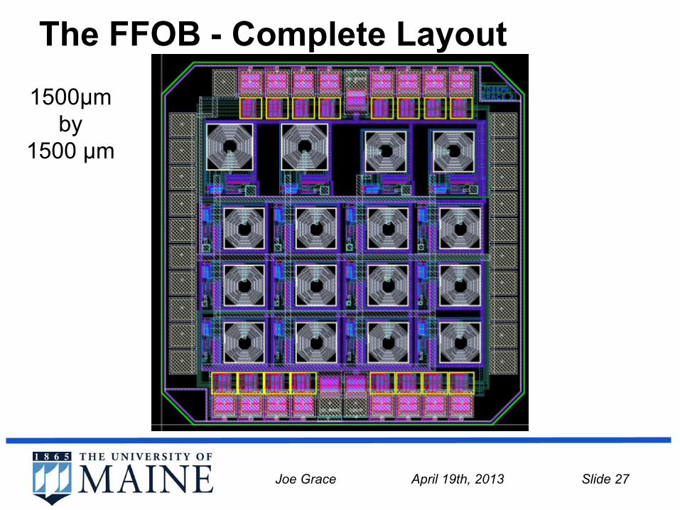
The FFOB - Complete Layout
Joe Grace April 19th, 2013 Slide 27
1500μm by
1500 μm

The FFOB - Simulation Results
FFOB 1100 MHz Oscillator in Frequency Domain
Joe Grace April 19th, 2013 Slide 28
Mag
nitu
de (m
A)
-36.5dB
-52.9dB
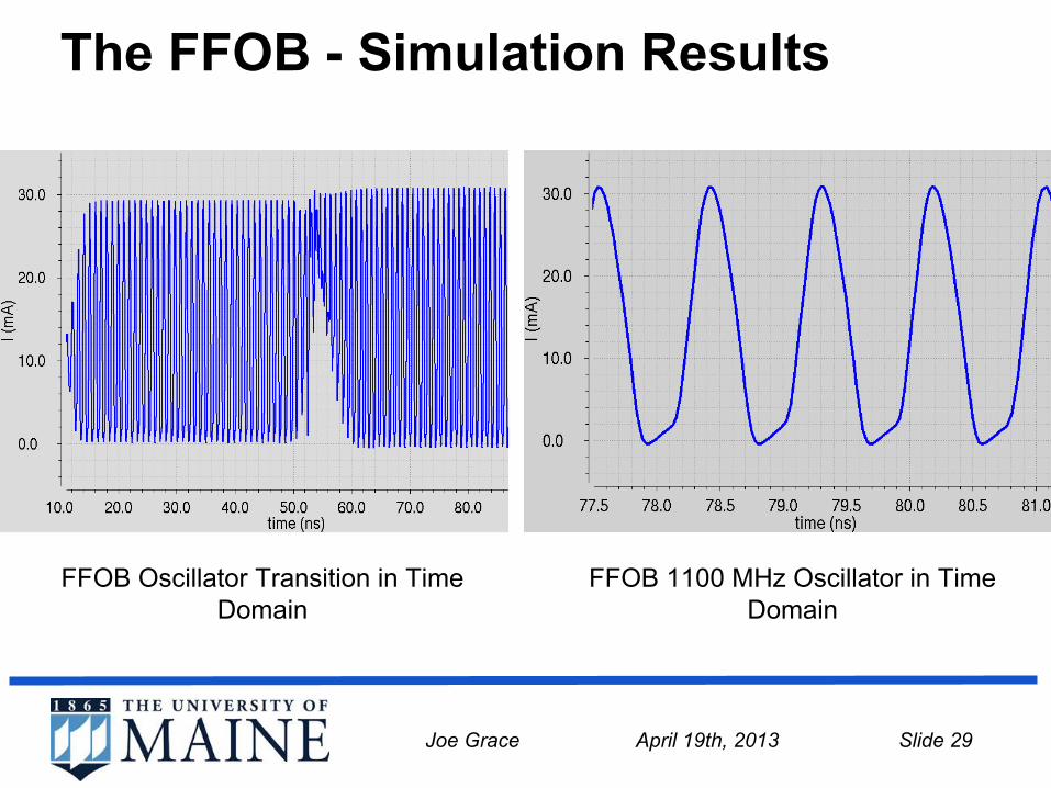
The FFOB - Simulation Results
FFOB 1100 MHz Oscillator in Time Domain
Joe Grace April 19th, 2013 Slide 29
FFOB Oscillator Transition in Time Domain

FFOB - Complete Simulation Results
Joe Grace April 19th, 2013 Slide 30
Target Freq
Simulated Freq

FFOB - Manufactured Chip - Test PCB
Joe Grace April 19th, 2013 Slide 31
A two layer PCB was designed to test the manufactured chip.
A PIC18 microcontroller was used with 16 of its I/O pins controlling the FFOB.
Also included:Voltage regulator,switches, SMA connector output

FFOB - Manufactured Chip - Test PCB
These images show the PCB with components in place and is ready for test.
Joe Grace April 19th, 2013 Slide 32
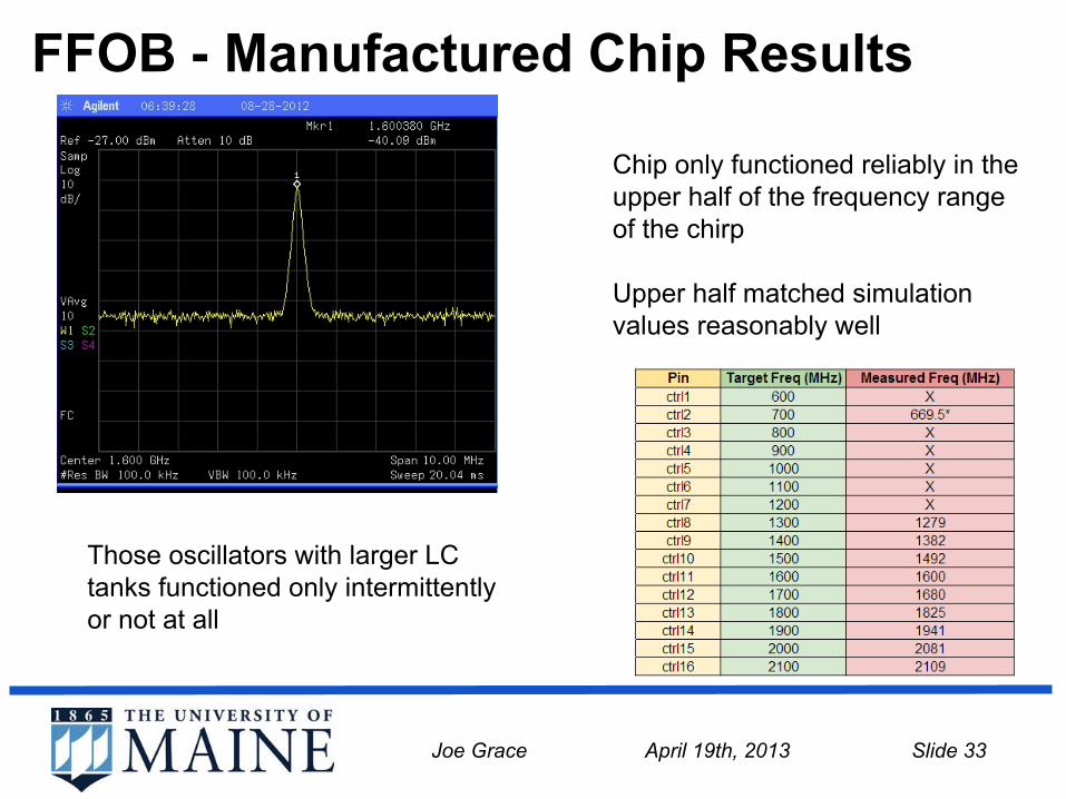
FFOB - Manufactured Chip Results
Joe Grace April 19th, 2013 Slide 33
Chip only functioned reliably in the upper half of the frequency range of the chirp
Upper half matched simulation values reasonably well
Those oscillators with larger LC tanks functioned only intermittently or not at all

FFOB - Measurements vs Simulation
Joe Grace April 19th, 2013 Slide 34
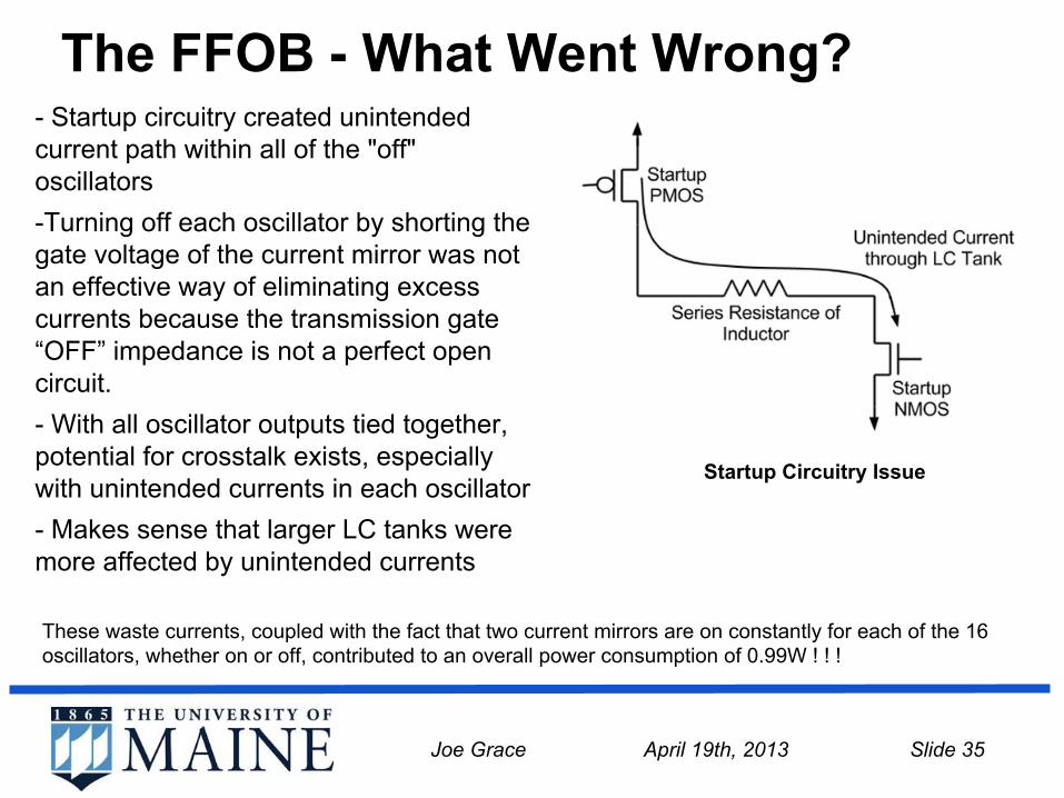
The FFOB - What Went Wrong?- Startup circuitry created unintended current path within all of the "off" oscillators-Turning off each oscillator by shorting the gate voltage of the current mirror was not an effective way of eliminating excess currents because the transmission gate “OFF” impedance is not a perfect open circuit. - With all oscillator outputs tied together, potential for crosstalk exists, especially with unintended currents in each oscillator- Makes sense that larger LC tanks were more affected by unintended currents
Joe Grace April 19th, 2013 Slide 35
These waste currents, coupled with the fact that two current mirrors are on constantly for each of the 16 oscillators, whether on or off, contributed to an overall power consumption of 0.99W ! ! !
Startup Circuitry Issue

The VCOB: An Improved Design● Uses 8 voltage controlled oscillators in design, each using a
varactor to generate a range of frequencies
● 32 discrete frequencies generated every 50 MHz from 1.5 GHz to 3.05 GHz, twice as many points as FFOB over a similar bandwidth
● Single output that drives a 50 Ohm load with an output swing from -2mA to +2mA
● 5 inputs:○ A clock signal that determines the chirp period (maximum
frequency is 500 MHz, which results in a 128 ns chirp period)○ 4 varactor DC bias voltages (1.1, 1.5, 2.2, and 3.2V)
Joe Grace April 19th, 2013 Slide 36
The VCOB- Why is it better?● Startup circuitry changed to a
single PMOS pull up transistor on unused oscillator output (no current path to ground in off state)
● TX gate used to cut off Vdd entirely from unused oscillators, not just the gate connection of current mirror
● TX gate on the output of every oscillator output to prevent crosstalk between oscillators
● Single output stage for all oscillators to reduce chip space and power consumption
Joe Grace April 19th, 2013 Slide 37
● Each oscillator output tuned to produce consistent output amplitude and is better matched to the linear range of the VTC of the SF output stage
● Each oscillator transistors sized individually to prevent saturation but maintain output swing
● 1.8V, 180 nm gate length transistors used to allow for the use of varactors for better frequency tunability
● Digital timing circuit implemented to automatically cycle through oscillation frequencies without the need for off-chip control

The VCOB Block Diagram
Joe Grace April 19th, 2013 Slide 38
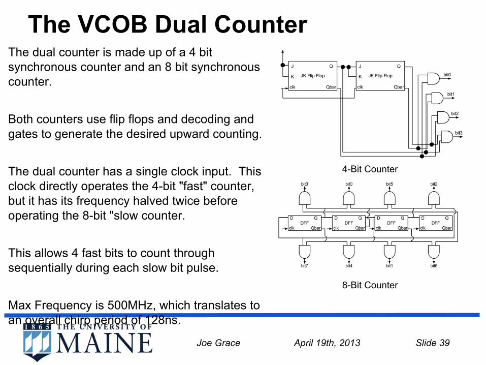
The VCOB Dual Counter
Joe Grace April 19th, 2013 Slide 39
4-Bit Counter
8-Bit Counter
The dual counter is made up of a 4 bit synchronous counter and an 8 bit synchronous counter.
Both counters use flip flops and decoding and gates to generate the desired upward counting.
The dual counter has a single clock input. This clock directly operates the 4-bit "fast" counter, but it has its frequency halved twice before operating the 8-bit "slow counter.
This allows 4 fast bits to count through sequentially during each slow bit pulse.
Max Frequency is 500MHz, which translates to an overall chirp period of 128ns.

The VCOB Dual Counter - Fast Bits
Joe Grace April 19th, 2013 Slide 40
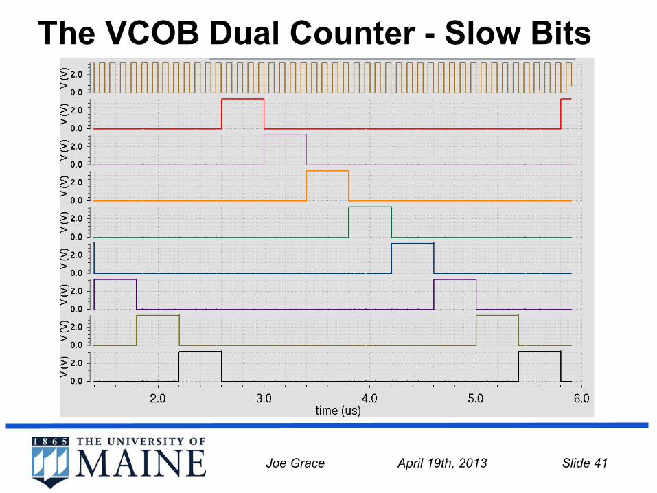
The VCOB Dual Counter - Slow Bits
Joe Grace April 19th, 2013 Slide 41

The VCOB Oscillator
Joe Grace April 19th, 2013 Slide 42

The VCOB Oscillator
Joe Grace April 19th, 2013 Slide 43
LC Oscillatorwith varactor

The VCOB Oscillator
Joe Grace April 19th, 2013 Slide 44
Current cutoffTX gate

The VCOB Oscillator
Joe Grace April 19th, 2013 Slide 45
Single startuppull-up PMOS

The VCOB Oscillator
Joe Grace April 19th, 2013 Slide 46
TX gate isolatingoscillator outputs

The VCOB Output Stage
Joe Grace April 19th, 2013 Slide 47
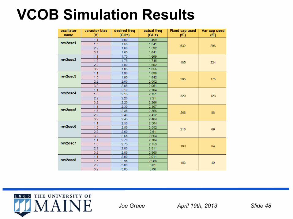
VCOB Simulation Results
Joe Grace April 19th, 2013 Slide 48

VCOB Simulation Results
Joe Grace April 19th, 2013 Slide 49
1.85 GHz Oscillator in Frequency Domain1.85 GHz Oscillator in Time Domain
Mag
nitu
de (m
A)
-55.9dB
-84.5dB

The VCOB- Complete Layout
Joe Grace April 19th, 2013 Slide 50
1500μm by
1500 μm
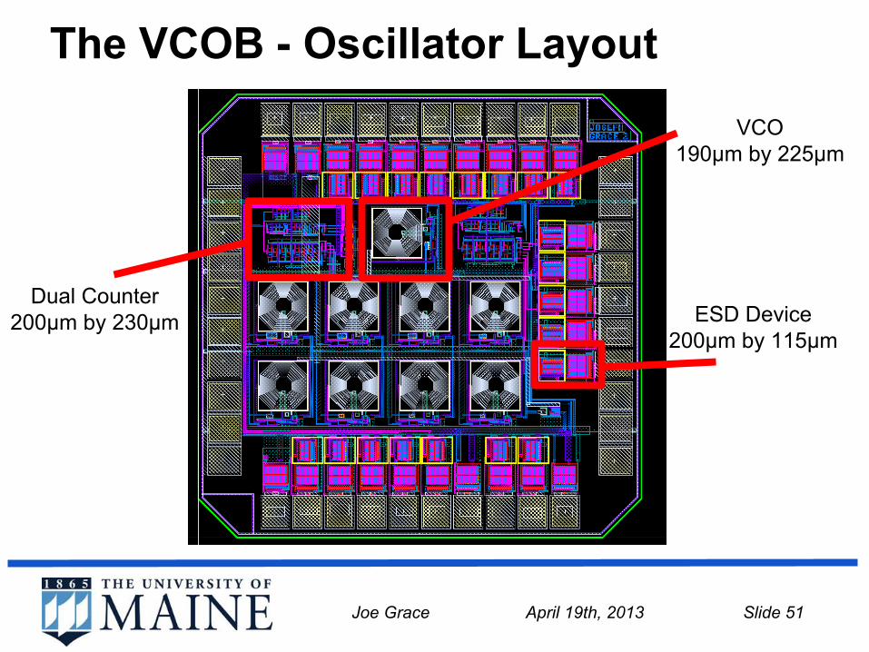
The VCOB - Oscillator Layout
Joe Grace April 19th, 2013 Slide 51
VCO190μm by 225μm
ESD Device200μm by 115μm
Dual Counter200μm by 230μm

VCOB Summary
Joe Grace April 19th, 2013 Slide 52
● 32 discrete frequencies generated by 8 VCOs ( Improved from 16 discrete frequencies generated by 16 separate fixed oscillators in FFOB design)
● 3.3V and 1.8V dual supply utilized with both analog and digital circuitry (just 3.3V in FFOB)
● 18mW of power consumed while running (Down from 990mW in FFOB design)
● Oscillator reliability, uniformity, 2nd harmonic distortion all improved over FFOB design
● Clock input sets chirp period and each oscillator is controlled by on-chip digital counters (controlled off-chip in FFOB design)

Conclusions
Joe Grace April 19th, 2013 Slide 53
● Two LC Oscillator ICs have been designed to function as a chirp generator for a LADAR system○ Fixed Frequency Oscillator Bank (FFOB)
■ Design, Simulation, Layout, Manufacture, and Testing Complete○ Voltage Controlled Oscillator Bank (VCOB)
■ Design, Simulation, and Layout Complete
● Abstract submitted to IEEE Sensors Conference this November in Baltimore, acceptance pending
J. R. Grace III et al., "LC Oscillator Chirp Generator for LADAR Sensing Applications," submitted to IEEE Sensors Conference, Baltimore, MD, November 2013.
● Future work in this area might include:○ Have the VCOB manufactured and tested○ Integrate this CMOS chirp generator with other LADAR
subsystems onto one CMOS IC
Q & A
Joe Grace April 19th, 2013 Slide 54