ii CENTRAL POLYTECHNIC COLLEGE Tharamani - chennai-113. PROJECT REPORT(2014-2015) DEVELOPMENT OF COMPUTER VISSION SYSTEM FOR VISUALLY IMPAIRED Submitted in partial full fillment for the award of diploma in ELECTRONICS AND COMMUNICATION ENGINEERING GUIDED BY Mr.T.PADMANATHAN.,B.E DONE BY S.GOWTHAM 401112019 S.LOGESWARAN 401112041 S.MANOJ KUMAR 401112046 S.PONNAIYAN 401112060 M.PRASANTH 401112062 K.PRATHAP 401112064

Welcome message from author
This document is posted to help you gain knowledge. Please leave a comment to let me know what you think about it! Share it to your friends and learn new things together.
Transcript
ii
CENTRAL POLYTECHNIC COLLEGE
Tharamani - chennai-113.
PROJECT REPORT(2014-2015)
DEVELOPMENT OF COMPUTER VISSION
SYSTEM FOR VISUALLY IMPAIRED
Submitted in partial full fillment for the award of diploma in
ELECTRONICS AND COMMUNICATION ENGINEERING
GUIDED BY
Mr.T.PADMANATHAN.,B.E
DONE BY
S.GOWTHAM 401112019
S.LOGESWARAN 401112041
S.MANOJ KUMAR 401112046
S.PONNAIYAN 401112060
M.PRASANTH 401112062
K.PRATHAP 401112064
ii
CENTRAL POLYTECHNIC COLLEGE, THARAMANI,CHENNAI-113
DEPARTMENT OF ELECTRONICS AND COMMUNICATION
ENGINEERING
PROJECT REPORT
(2014-2015)
BONAFIDE CERTIFICATE
This is to certify that this is a bonafide record of the project work
done by
Selvan........................................... Reg. no................... of final year
Diploma in ELECTRONICS AND COMMUNICATION
ENGINEERING who carried out the project work under my
supervision during the Academic Year 2014-2015. submitted for
board examination held on.................
MARKS AWARDED: __/25
PROJECT GUIDE HEAD OF THE DEPARTMENT
INTERNAL EXAMINER EXTERNAL EXAMINER

ii
ACKNOWLEDGEMENT
First of all, would like to express our sincere thanks to our parents
creating us as diploma engineers.
Next our thanks to our honourable THE DIRECTOR, DIRECTORATE OF
TECHNICAL EDUCATION who made me our ways full of light will a
kind heart to achieve our targets.
We would all so like to thank our honourable principle.
DR.SOKKALINGAM. M.E., Ph.D.,who leads our college in a
respectable manner.
We thank our respectable Head of the Department
Mr.JAYAPAL for providing us more facilities and also for the great
encouragement while doing our project.
We thank our respectable project guide
Mr.T.PADMANATHAN.,B.E.,for his valuable suggestions.
We would thank our department staff and other department staffs
for providing us a great support by helping in various times to finish
our project.

ii
PREFACE
PROJECT WORK IMPORTANCE
Project work plays an important role in technical education.
With working through the project, students are exposed to
different fields in production.
Thus the students get an opportunity to make use of his
knowledge, skill and ability in the design, fabrication and
erection of the project.
He even learns new subjects and practical works as well. He
gains great experience in getting ideas in organizing the work
and putting them into practice.
He learns to approach various problems systematically,
thereby constructing a project and improving his knowledge.
ii
CONTENTS
CHAPTERS page no
1. INTRODUCTION . . .6
2. AIM OF THE PROJECT . . .7
3. SYSTEM DESIGN . . .8
BLOCK DIAGRAM BLOCK DESCRIPTION
CIRCUIT DIAGRAM
CIRCUIT DESCRIPTION
PIC MICROCONTROLLER 16F877A
POWER SUPPLY
MAX 232
APR 9600 VOICE IC
LCD MODULE
MPLAB IDE V8
4. SYSTEM SOFTWARE . . .59
5. CONCLUSION . . .69
ii
INTRODUCTION
The Embedded Technology is now in its prime and
the wealth of Knowledge available is mind-blowing.
Embedded System is a combination of hardware
and software. Embedded technology plays a major
role in integrating the various functions associated
with it.
This needs to tie up the various sources of the
Department in a closed loop system. This proposal
greatly reduces the manpower, saves time and
operates efficiently without human interference.
Basedon statistics from the World Health
Organization (WHO), there are more than 161
million visually impaired people around the world,
and 37 million of them are blind.
Choosing clothes with suitable colors and patterns is
a challenging task for blind or visually impaired
people.
ii
AIM OF PROJECT
The aim of the project is about DEVELOPMENT OF
COMPUTER VISSION SYSTEM FOR VISUALLY
IMPAIRED
METHODOLOGY:
With the help of PIC microcontroller and WEB camerais used to find the
person and path without anyone help.
WORKING PRINCIPLE:
The system integrates a camera, a microphone, a
computer, and a speaker for audio description of certain
objects.
A camera is used to capture the certain objects like table,
chair. Also person face recognition is done for
authentication.
The detected object and status of the system displayed on
LCD. Also the voice is alerted using APR.
ADVANTAGES:
Very much helpful for blind people
More reliable system
Portable
ii
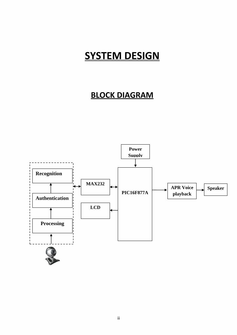
SYSTEM DESIGN
BLOCK DIAGRAM
Power
Supply
PIC16F877A
MAX232 APR Voice
playback
Speaker
Recognition
Authentication
Processing
LCD
ii
BLOCK DESCRIPTION:
POWER SUPPLY
PIC MICROCONTROLLER
MAX 232
LCD MODULE
APR 9600 VOICE IC
MPLAM COMPILER

ii
BLOCK 1: POWER SUPPLY
Power Supply for PIC 16F877A Microcontroller
This section describes how to generate +5V DC power supply
The power supply section is the important one. It should
deliver constant output regulated power supply for successful
working of the project. A 0-12V/1 mA transformer is used for
this purpose.
The primary of this transformer is connected in to main
supply through on/off switch& fuse for protecting from
overload and short circuit protection. The secondary is
connected to the diodes to convert 12V AC to 12V DC voltage.
And filtered by the capacitor. Which is further regulated to
+5v, by using IC 7805.
ii
BLOCK 2: PIC MICROCONTROLLER
INTRODUCTION OF PIC16F877A:
The PIC16F877A CMOS FLASH-based 8-bit microcontroller is upward
compatible with the PIC16C5x, PIC12Cxxx and PIC16C7x devices. It
features 200 ns instruction execution, 256 bytes of EEPROM data
memory, self programming, an ICD, 2 Comparators, 8 channels of 10-bit
Analog-to-Digital (A/D) converter, 2 capture/compare/PWM functions, a
synchronous serial port that can be configured as either 3-wire SPI or 2-
wire I2C bus, a USART, and a Parallel Slave Port.
Microchip PIC16F877A Microcontroller Features:
High-Performance RISC CPU
Operating speed: 20 MHz, 200 ns instruction cycle Operating voltage: 4.0-5.5V Industrial temperature range (-40° to +85°C) 15 Interrupt Sources 35 single-word instructions All single-cycle instructions except for program branches (two-
cycle)
Special Microcontroller Features
Flash Memory: 14.3 Kbytes (8192 words) Data SRAM: 368 bytes Data EEPROM: 256 bytes Self-reprogrammable under software control In-Circuit Serial Programming via two pins (5V) Watchdog Timer with on-chip RC oscillator Programmable code protection

ii
Power-saving Sleep mode Selectable oscillator options In-Circuit Debug via two pins
Peripheral Features
33 I/O pins; 5 I/O ports Timer0: 8-bit timer/counter with 8-bit prescaler Timer1: 16-bit timer/counter with prescaler
o Can be incremented during Sleep via external crystal/clock Timer2: 8-bit timer/counter with 8-bit period register, prescaler and
prescaler Two Capture, Compare, PWM modules
o 16-bit Capture input; max resolution 12.5 ns o 16-bit Compare; max resolution 200 ns o 10-bit PWM
Synchronous Serial Port with two modes: o SPI Master o I2C Master and Slave
USART/SCI with 9-bit address detection Parallel Slave Port (PSP)
o 8 bits wide with external RD, WR and CS controls Brown-out detection circuitry for Brown-Out Reset
Analog Features
10-bit, 8-channel A/D Converter Brown-Out Reset Analog Comparator module
o 2 analog comparators o Programmable on-chip voltage reference module
ii
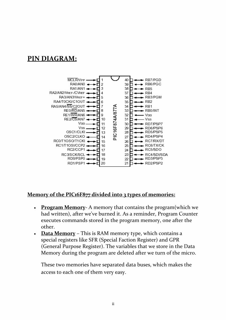
PIN DIAGRAM:
Memory of the PIC16F877 divided into 3 types of memories:
Program Memory- A memory that contains the program(which we had written), after we've burned it. As a reminder, Program Counter executes commands stored in the program memory, one after the other.
Data Memory – This is RAM memory type, which contains a special registers like SFR (Special Faction Register) and GPR (General Purpose Register). The variables that we store in the Data Memory during the program are deleted after we turn of the micro.
These two memories have separated data buses, which makes the
access to each one of them very easy.
ii
Data EEPROM (Electrically Erasable Programmable Read-Only Memory)- A memory that allows storing the variables as a result of burning the written program.
Each one of them has a different role. Program Memory and Data Memory
two memories that are needed to build a program, and Data EEPROM is
used to save data after the microcontroller is turn off.
Program Memory and Data EEPROM they are non-volatile memories,
which store the information even after the power is turn off. These
memories called Flash Or EEPROM. In contrast, Data Memory does not
save the information because it needs power in order to maintain the
information stored in the chip.
PIC16F87XA Program Memory
The PIC16F87XA devices have a 13-bit program counter capable
of addressing an 8K word x 14 bit program memory space. This
memory is used to store the program after we burn it to the
microcontroller. The PIC16F876A/877A devices have 8K words x
14 bits of Flash program memory that can be electrically erased
and reprogrammed. Each time we burn program into the micro,
we erase an old program and write a new one.
ii
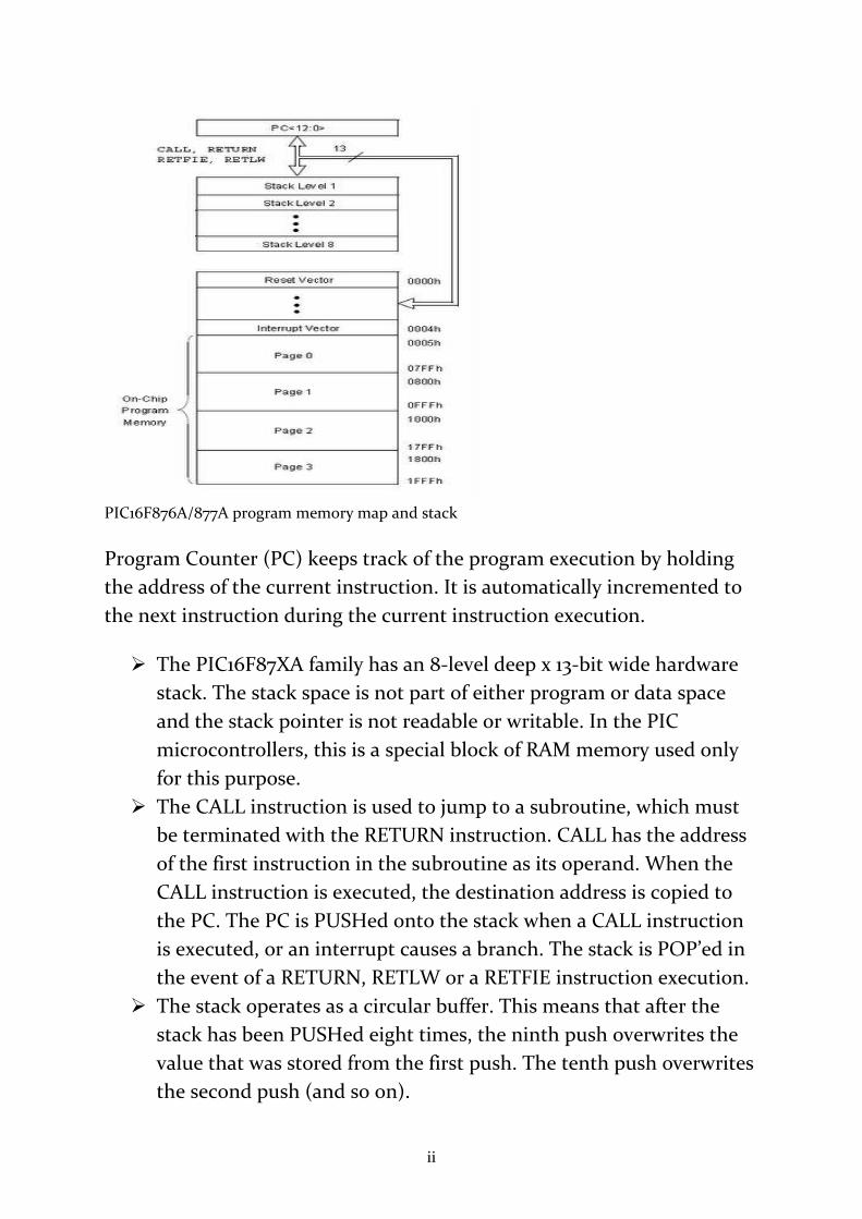
PIC16F876A/877A program memory map and stack
Program Counter (PC) keeps track of the program execution by holding
the address of the current instruction. It is automatically incremented to
the next instruction during the current instruction execution.
The PIC16F87XA family has an 8-level deep x 13-bit wide hardware
stack. The stack space is not part of either program or data space
and the stack pointer is not readable or writable. In the PIC
microcontrollers, this is a special block of RAM memory used only
for this purpose.
The CALL instruction is used to jump to a subroutine, which must
be terminated with the RETURN instruction. CALL has the address
of the first instruction in the subroutine as its operand. When the
CALL instruction is executed, the destination address is copied to
the PC. The PC is PUSHed onto the stack when a CALL instruction
is executed, or an interrupt causes a branch. The stack is POP’ed in
the event of a RETURN, RETLW or a RETFIE instruction execution.
The stack operates as a circular buffer. This means that after the
stack has been PUSHed eight times, the ninth push overwrites the
value that was stored from the first push. The tenth push overwrites
the second push (and so on).
ii
Each time the main program execution starts at address 0000 -
Reset Vector. The address 0004 is “reserved” for the “interrupt
service routine” (ISR).
If we plan to use an interrupt, our program will begin after the
Interrupt Vector; and if not we can start to write from the beginning
of the Reset Vector.
Some of the memory is divided into the pages that are designed for
write/burn the program into them; the remaining memory (Stack,
Interrupt Vector, and Reset Vector) is hardware registers.
Attention!
Program Memory is divided into the pages, where the program is stored.
Data Memory is divided into the banks. The banks are located inside the
RAM, where the special registers and the data located.
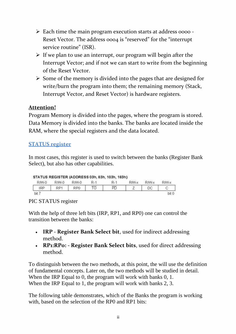
STATUS register
In most cases, this register is used to switch between the banks (Register Bank
Select), but also has other capabilities.
PIC STATUS register
With the help of three left bits (IRP, RP1, and RP0) one can control the
transition between the banks:
IRP - Register Bank Select bit, used for indirect addressing method.
RP1:RP0: - Register Bank Select bits, used for direct addressing method.
To distinguish between the two methods, at this point, the will use the definition
of fundamental concepts. Later on, the two methods will be studied in detail.
When the IRP Equal to 0, the program will work with banks 0, 1.
When the IRP Equal to 1, the program will work with banks 2, 3.
The following table demonstrates, which of the Banks the program is working
with, based on the selection of the RP0 and RP1 bits:
ii
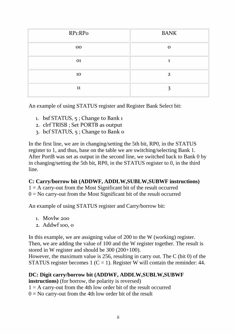
RP1:RP0 BANK
00 0
01 1
10 2
11 3
An example of using STATUS register and Register Bank Select bit:
1. bsf STATUS, 5 ; Change to Bank 1 2. clrf TRISB ; Set PORTB as output 3. bcf STATUS, 5 ; Change to Bank 0
In the first line, we are in changing/setting the 5th bit, RP0, in the STATUS
register to 1, and thus, base on the table we are switching/selecting Bank 1.
After PortB was set as output in the second line, we switched back to Bank 0 by
in changing/setting the 5th bit, RP0, in the STATUS register to 0, in the third
line.
C: Carry/borrow bit (ADDWF, ADDLW,SUBLW,SUBWF instructions) 1 = A carry-out from the Most Significant bit of the result occurred
0 = No carry-out from the Most Significant bit of the result occurred
An example of using STATUS register and Carry/borrow bit:
1. Movlw 200 2. Addwf 100, 0
In this example, we are assigning value of 200 to the W (working) register.
Then, we are adding the value of 100 and the W register together. The result is
stored in W register and should be 300 (200+100).
However, the maximum value is 256, resulting in carry out. The C (bit 0) of the
STATUS register becomes 1 (C = 1). Register W will contain the reminder: 44.
DC: Digit carry/borrow bit (ADDWF, ADDLW,SUBLW,SUBWF
instructions) (for borrow, the polarity is reversed)
1 = A carry-out from the 4th low order bit of the result occurred
0 = No carry-out from the 4th low order bit of the result

ii
Z: Zero bit 1 = The result of an arithmetic or logic operation is zero
0 = The result of an arithmetic or logic operation is not zero
The bits 3 and 4 are used with WDT - Watchdog Timer.
PD: Power-down bit 1 = After power-up or by the CLRWDT instruction
0 = By execution of the SLEEP instruction
TO: Time-out bit 1 = After power-up, CLRWDT instruction or SLEEP instruction
0 = A WDT time-out occurred
PORT register
The role of the PORT register is to receive the information from an external
source (e.g. sensor) or to send information to the external elements (e.g. LCD).
ii
We can control each port by using an assigned address of specific port, but there
is much easier way to control the port. We are allowed to use the names of the
ports without considering their addresses.
For example:
# define SWITCH PORTA, 0
We define a variable named SWITCH, which received a value of bit number 0
of the PORTA. Usually we define the ports at the beginning of the program, and
then we use only the given names.
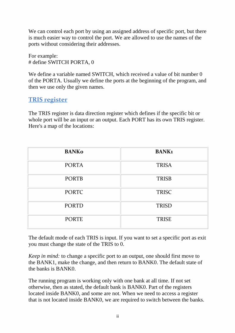
TRIS register
The TRIS register is data direction register which defines if the specific bit or
whole port will be an input or an output. Each PORT has its own TRIS register.
Here's a map of the locations:
BANK0 BANK1
PORTA TRISA
PORTB TRISB
PORTC TRISC
PORTD TRISD
PORTE TRISE
The default mode of each TRIS is input. If you want to set a specific port as exit
you must change the state of the TRIS to 0.
Keep in mind: to change a specific port to an output, one should first move to
the BANK1, make the change, and then return to BANK0. The default state of
the banks is BANK0.
The running program is working only with one bank at all time. If not set
otherwise, then as stated, the default bank is BANK0. Part of the registers
located inside BANK0, and some are not. When we need to access a register
that is not located inside BANK0, we are required to switch between the banks.
ii
For example, the access to PORT registers is done inside BANK0. However, to
change port from an input to an output and vice versa, we need to access TRIS
register that is located inside BANK1. From the moment we moved to the
BANK1, the program will always work with BANK1; at this time, to access
registers inside BANK0, we will have to return to the situation in which our
program will work with BANK0.
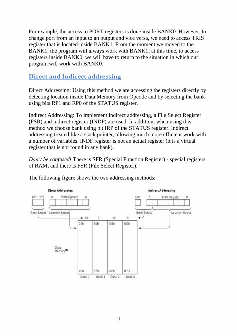
Direct and Indirect addressing
Direct Addressing: Using this method we are accessing the registers directly by
detecting location inside Data Memory from Opcode and by selecting the bank
using bits RP1 and RP0 of the STATUS register.
Indirect Addressing: To implement indirect addressing, a File Select Register
(FSR) and indirect register (INDF) are used. In addition, when using this
method we choose bank using bit IRP of the STATUS register. Indirect
addressing treated like a stack pointer, allowing much more efficient work with
a number of variables. INDF register is not an actual register (it is a virtual
register that is not found in any bank).
Don’t be confused! There is SFR (Special Function Register) - special registers
of RAM, and there is FSR (File Select Register).
The following figure shows the two addressing methods:
ii
To the left you can see the direct addressing method, where the bank selection is
made by RP bits and the referencing is made directly from memory Opcode by
using the variable name.
To the right you can see the indirect addressing method, where the bank
selection is made by IRP bit and accessing the variable by pointer FSR.
Let’s explore the differences between the 2 methods:
We want to assign number 5 to the variable TEMP located at address 0X030. In
the first row of each example, we will define the variable TEMP at the address
0X030.
Example of direct addressing:
1. TEMP Equ 0x030 2. Movlw 5 3. Movwf TEMP
It's easy to understand, that direct addressing method means working directly
with the variables. In the second line we put the number 5 into the working
register W, and in the line 3, the content of the W passes to the TEMP variable.
Example of indirect addressing:
1. TEMP Equ 0x030 2. Movlw 0x030 3. Movwf FSR 4. Movlw 5 5. Movwf INDF
In the second line, we put a value into the W register. In the third line, the value
passes to the FSR register, and from this moment FSR points to the address of
the TEMP variable. In the fourth line, the number 5 passes to the W register,
and in the fifth line, we move the contents of W register (which is 5) to the
INDF. In fact INDF performs the following: it takes the number 5 and puts it in
the address indicated by FSR register.
ii
PIC16F87XA Data EEPROM
The data EEPROM and Flash program memory is readable and writable during
normal operation (over the full VDD range). This memory is not directly
mapped in the register file space. Instead, it is indirectly addressed through the
Special Function Registers.
There are six SFRs used to read and write to this memory:
1. EECON1 2. EECON2 3. EEDATA 4. EEDATH 5. EEADR 6. EEADRH
When interfacing to the data memory block, EEDATA holds the 8-bit data for
read/write and EEADR holds the address of the EEPROM location being
accessed. These devices have 128 or 256 bytes of data EEPROM (depending on
the device), with an address range from 00h to FFh. On devices with 128 bytes,
addresses from 80h to FFh are unimplemented.
A few important points about Data EEPROM memory:
It lets you save data DURING programming The data is saved during the “burning” process You can read the data memory during the programming and use it The use is made possible with the help of SFR
At this point there is no need to learn how to use this memory with special
registers, because there are functions (writing and reading) that are ready.
Write to DATA EEPROM
To write to an EEPROM data location, the user must first write the address to
the EEADR register and the data to the EEDATA register. Then the user must
follow a specific write sequence to initiate the write for each byte.
BSF STATUS, RP1 ;
BSF STATUS, RP0 ; Bank 3
BTFSC EECON1, WR ;Wait for write
ii
GOTO $-1 ;to complete
BCF STATUS, RP0 ;Bank 2
MOVF DATA_EE_ADDR, W ;Data Memory
MOVWF EEADR ;Address to write
MOVF DATA_EE_DATA, W ;Data Memory Value
MOVWF EEDATA ;to write
BSF STATUS, RP0 ;Bank 3
BCF EECON1, EEPGD ;Point to DATA memory
BSF EECON1, WREN ;Enable writes
BCF INTCON, GIE ;Disable INTs.
MOVLW 55h ;
MOVWF EECON2 ;Write 55h
MOVLW AAh ;
MOVWF EECON2 ;Write AAh
BSF EECON1, WR ;Set WR bit to begin write
BSF INTCON, GIE ;Enable INTs
BCF EECON1, WREN ;Disable writes
Read DATA EEPROM
To read a data memory location, the user must write the address to the
EEADR register, clear the EEPGD control bit (EECON1<7>) and then set
control bit RD (EECON1<0>). The data is available in the very next cycle
in the EEDATA register; therefore, it can be read in the next instruction.
EEDATA will hold this value until another read or until it is written to by
the user (during a write operation).
BSF STATUS, RP1 ;
BCF STATUS, RP0 ; Bank 2
MOVF DATA_EE_ADDR, W ; Data Memory
MOVWF EEADR ; Address to read
BSF STATUS, RP0 ; Bank 3
BCF EECON1, EEPGD ; Point to Data memory
BSF EECON1, RD ; EE Read
BCF STATUS, RP0 ; Bank 2
MOVF EEDATA, W ; W = EEDATA
ii
Both of these functions are provided by the manufacturer. There is a
required sequence in order to write/read to/from the memory; that
process can be performed independently, but it is better to use ready
functions of Microchip.
PIC Timer0:
Many times, we plan and build systems that perform various processes
that depend on time.
Simple example of this process is the digital wristwatch. The role of this
electronic system is to display time in a very precise manner and change
the display every second (for seconds), every minute (for minutes) and so
on.
To perform the steps we've listed, the system must use a timer, which
needs to be very accurate in order to take necessary actions. The clock is
actually a core of any electronic system.
In this PIC timer module tutorial we will study the existing PIC timer
modules. The microcontroller PIC16F877 has 3 different timers:
PIC Timer0 PIC Timer1 PIC Timer2
We can use these timers for various important purposes. So far we used
“delay procedure” to implement some delay in the program, that was
counting up to a specific value, before the program could be continued.
"Delay procedure" had two disadvantages:
we could not say exactly how long the Delay procedure was in progress
we could not perform any further steps while the program executes the "delay procedure"
Now, using Timers we can build a very precise time delays which will be
based on the system clock and allow us to achieve our desired time delay
well-known in advance.
ii
In order for us to know how to work with these timers, we need to learn
some things about each one of them. We will study each one separately.
PIC Timer0
The Timer0 module timer/counter has the following features:
8-bit timer/counter Readable and writable 8-bit software programmable prescaler Internal (4 Mhz) or external clock select Interrupt on overflow from FFh to 00h Edge select (rising or falling) for external clock
Let’s explain the features of PIC Timer0 we have listed above:
Timer0 has a register called TMR0 Register, which is 8 bits of size.
We can write the desired value into the register which will be increment
as the program progresses. Frequency varies depending on the Prescaler.
Maximum value that can be assigned to this register is 255.
TMR0IF - TMR0 Overflow Interrupt Flag bit.
The TMR0 interrupt is generated when the TMR0 register overflows from
FFh to 00h. This overflow sets bit TMR0IF (INTCON<2>). You can
initialize the value of this register to what ever you want (not necessarily
"0").
We can read the value of the register TMR0 and write into. We can reset
its value at any given moment (write) or we can check if there is a certain
numeric value that we need (read).
Prescaler - Frequency divider.
1:2
ii
1:4 1:8 1:16 1:32 1:64 1:128 1:256
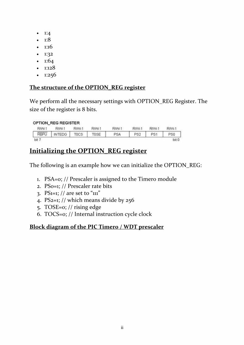
The structure of the OPTION_REG register
We perform all the necessary settings with OPTION_REG Register. The
size of the register is 8 bits.
Initializing the OPTION_REG register
The following is an example how we can initialize the OPTION_REG:
1. PSA=0; // Prescaler is assigned to the Timer0 module 2. PS0=1; // Prescaler rate bits 3. PS1=1; // are set to “111” 4. PS2=1; // which means divide by 256 5. TOSE=0; // rising edge 6. TOCS=0; // Internal instruction cycle clock
Block diagram of the PIC Timer0 / WDT prescaler
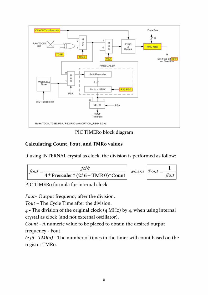
ii
PIC TIMER0 block diagram
Calculating Count, Fout, and TMR0 values
If using INTERNAL crystal as clock, the division is performed as follow:
PIC TIMER0 formula for internal clock
Fout– Output frequency after the division.
Tout – The Cycle Time after the division.
4 - The division of the original clock (4 MHz) by 4, when using internal
crystal as clock (and not external oscillator).
Count - A numeric value to be placed to obtain the desired output
frequency - Fout.
(256 - TMR0) - The number of times in the timer will count based on the
register TMR0.
ii
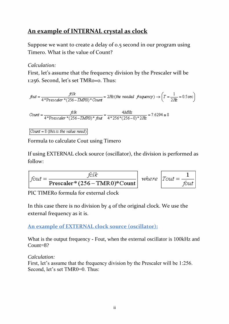
An example of INTERNAL crystal as clock
Suppose we want to create a delay of 0.5 second in our program using
Timer0. What is the value of Count?
Calculation:
First, let’s assume that the frequency division by the Prescaler will be
1:256. Second, let’s set TMR0=0. Thus:
Formula to calculate Cout using Timer0
If using EXTERNAL clock source (oscillator), the division is performed as
follow:
PIC TIMER0 formula for external clock
In this case there is no division by 4 of the original clock. We use the
external frequency as it is.
An example of EXTERNAL clock source (oscillator):
What is the output frequency - Fout, when the external oscillator is 100kHz and
Count=8?
Calculation:
First, let’s assume that the frequency division by the Prescaler will be 1:256.
Second, let’s set TMR0=0. Thus:
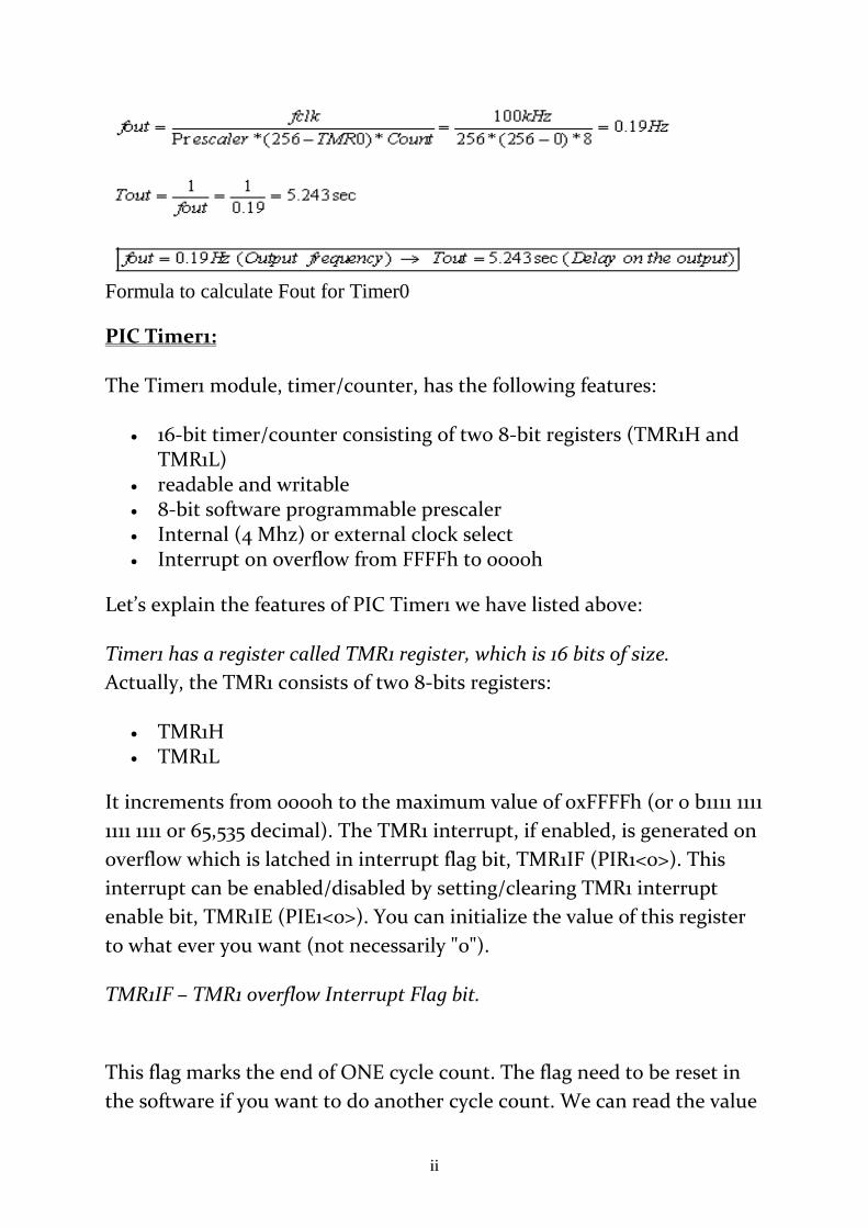
ii
Formula to calculate Fout for Timer0
PIC Timer1:
The Timer1 module, timer/counter, has the following features:
16-bit timer/counter consisting of two 8-bit registers (TMR1H and TMR1L)
readable and writable 8-bit software programmable prescaler Internal (4 Mhz) or external clock select Interrupt on overflow from FFFFh to 0000h
Let’s explain the features of PIC Timer1 we have listed above:
Timer1 has a register called TMR1 register, which is 16 bits of size.
Actually, the TMR1 consists of two 8-bits registers:
TMR1H TMR1L
It increments from 0000h to the maximum value of 0xFFFFh (or 0 b1111 1111
1111 1111 or 65,535 decimal). The TMR1 interrupt, if enabled, is generated on
overflow which is latched in interrupt flag bit, TMR1IF (PIR1<0>). This
interrupt can be enabled/disabled by setting/clearing TMR1 interrupt
enable bit, TMR1IE (PIE1<0>). You can initialize the value of this register
to what ever you want (not necessarily "0").
TMR1IF – TMR1 overflow Interrupt Flag bit.
This flag marks the end of ONE cycle count. The flag need to be reset in
the software if you want to do another cycle count. We can read the value
ii
of the register TMR1 and write into. We can reset its value at any given
moment (write) or we can check if there is a certain numeric value that
we need (read).
Prescaler – Frequency divider.
We can use Prescaler for further division of the system clock. The size of
the register is 2-bit only, so you can make four different division. The
options are:
1:1 1:2 1:4 1:8
You can choose whether to use an internal system clock (crystal) or
external oscillator that can be connected to a pin RC0.
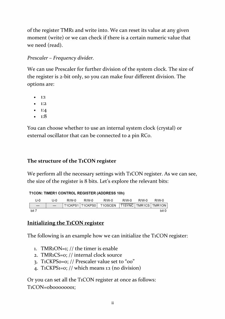
The structure of the T1CON register
We perform all the necessary settings with T1CON register. As we can see,
the size of the register is 8 bits. Let’s explore the relevant bits:
Initializing the T1CON register
The following is an example how we can initialize the T1CON register:
1. TMR1ON=1; // the timer is enable 2. TMR1CS=0; // internal clock source 3. T1CKPS0=0; // Prescaler value set to “00” 4. T1CKPS1=0; // which means 1:1 (no division)
Or you can set all the T1CON register at once as follows:
T1CON=0b00000001;
ii
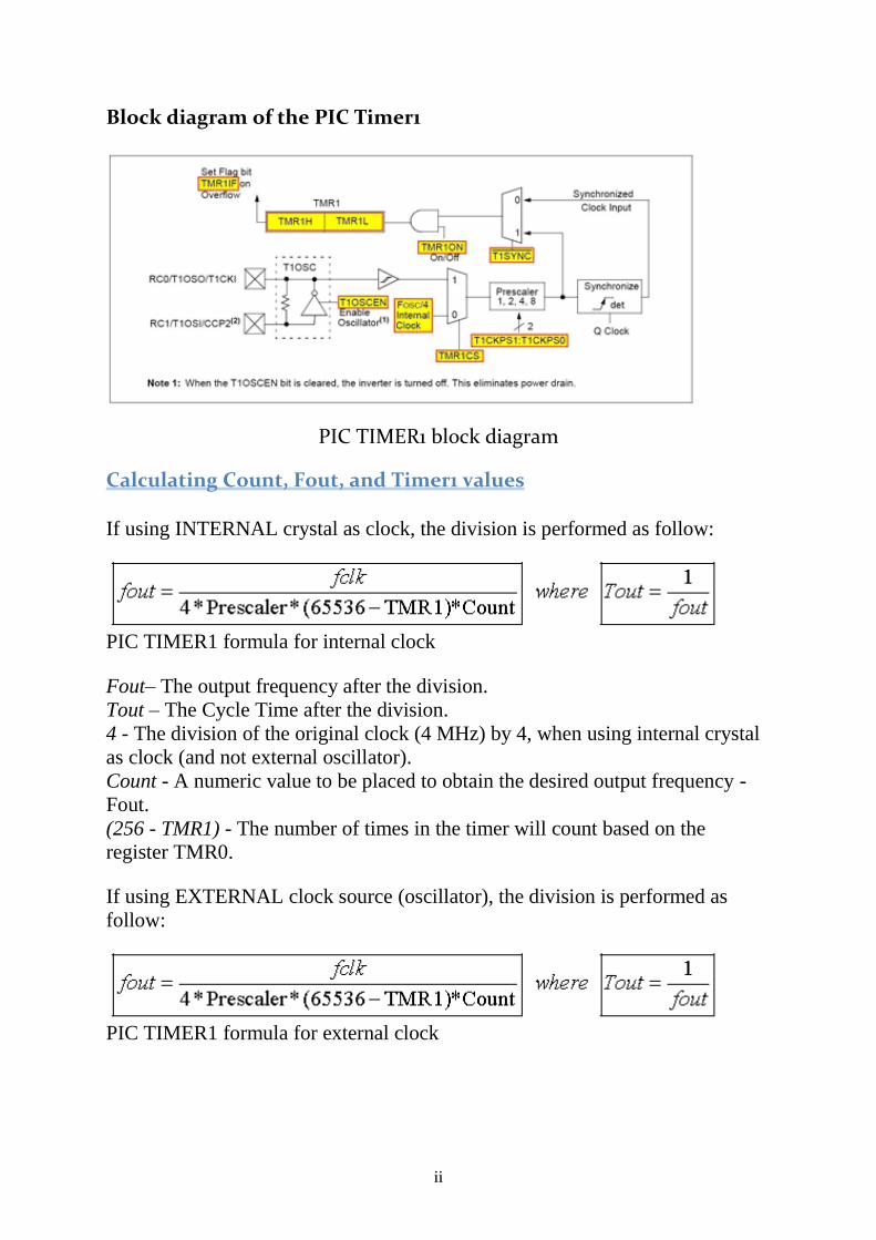
Block diagram of the PIC Timer1
PIC TIMER1 block diagram
Calculating Count, Fout, and Timer1 values
If using INTERNAL crystal as clock, the division is performed as follow:
PIC TIMER1 formula for internal clock
Fout– The output frequency after the division.
Tout – The Cycle Time after the division.
4 - The division of the original clock (4 MHz) by 4, when using internal crystal
as clock (and not external oscillator).
Count - A numeric value to be placed to obtain the desired output frequency -
Fout.
(256 - TMR1) - The number of times in the timer will count based on the
register TMR0.
If using EXTERNAL clock source (oscillator), the division is performed as
follow:
PIC TIMER1 formula for external clock
ii
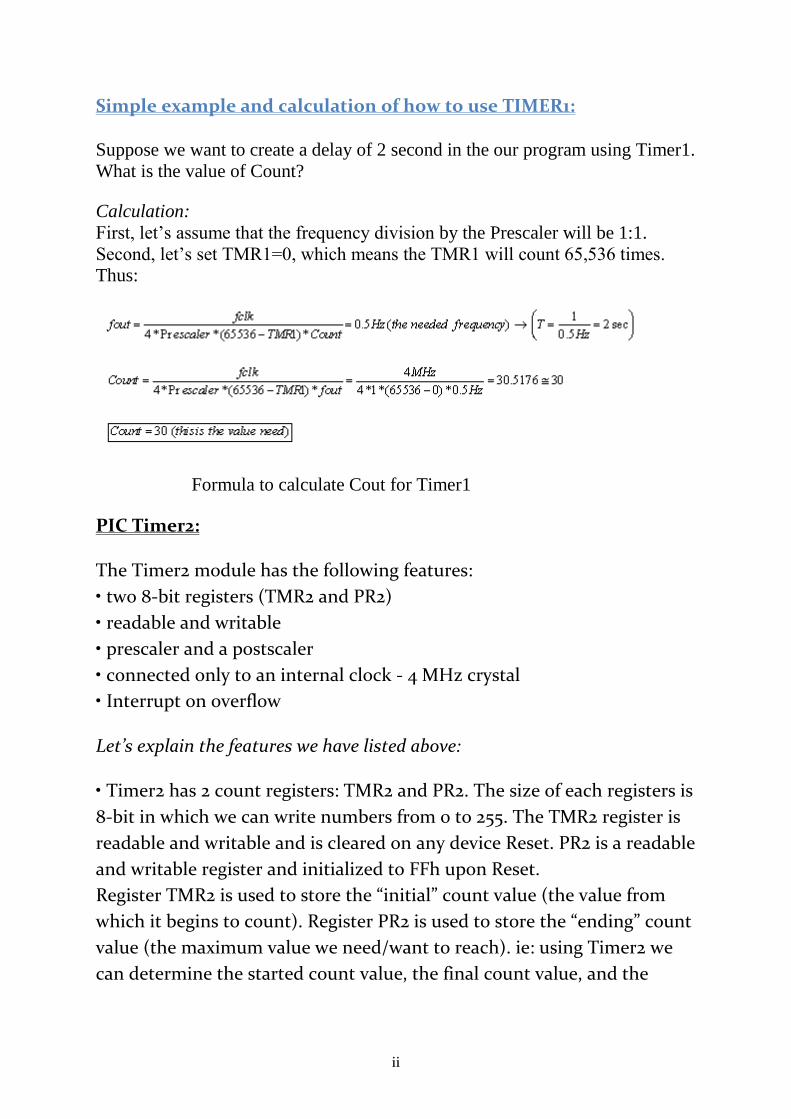
Simple example and calculation of how to use TIMER1:
Suppose we want to create a delay of 2 second in the our program using Timer1.
What is the value of Count?
Calculation:
First, let’s assume that the frequency division by the Prescaler will be 1:1.
Second, let’s set TMR1=0, which means the TMR1 will count 65,536 times.
Thus:
Formula to calculate Cout for Timer1
PIC Timer2:
The Timer2 module has the following features:
• two 8-bit registers (TMR2 and PR2)
• readable and writable
• prescaler and a postscaler
• connected only to an internal clock - 4 MHz crystal
• Interrupt on overflow
Let’s explain the features we have listed above:
• Timer2 has 2 count registers: TMR2 and PR2. The size of each registers is
8-bit in which we can write numbers from 0 to 255. The TMR2 register is
readable and writable and is cleared on any device Reset. PR2 is a readable
and writable register and initialized to FFh upon Reset.
Register TMR2 is used to store the “initial” count value (the value from
which it begins to count). Register PR2 is used to store the “ending” count
value (the maximum value we need/want to reach). ie: using Timer2 we
can determine the started count value, the final count value, and the
ii
count will be between these two values. The Timer2 increments from 00h
until it matches PR2 and then resets to 00h on the next increment cycle.
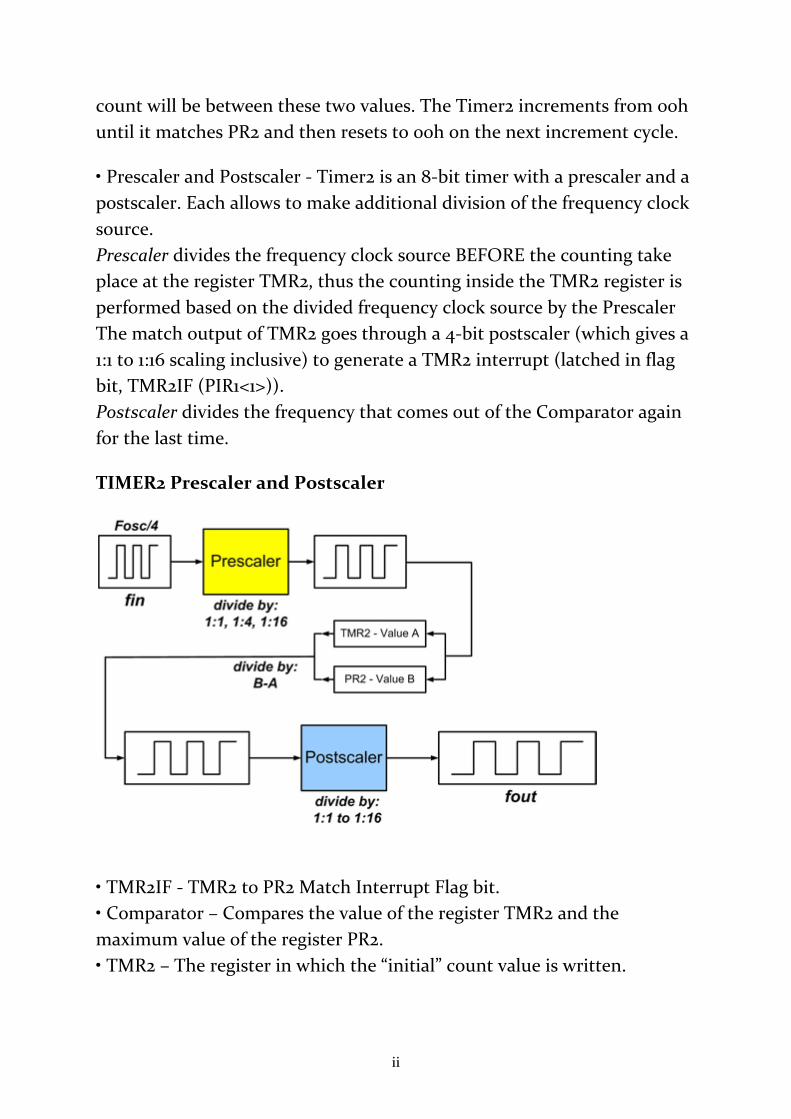
• Prescaler and Postscaler - Timer2 is an 8-bit timer with a prescaler and a
postscaler. Each allows to make additional division of the frequency clock
source.
Prescaler divides the frequency clock source BEFORE the counting take
place at the register TMR2, thus the counting inside the TMR2 register is
performed based on the divided frequency clock source by the Prescaler
The match output of TMR2 goes through a 4-bit postscaler (which gives a
1:1 to 1:16 scaling inclusive) to generate a TMR2 interrupt (latched in flag
bit, TMR2IF (PIR1<1>)).
Postscaler divides the frequency that comes out of the Comparator again
for the last time.
TIMER2 Prescaler and Postscaler
• TMR2IF - TMR2 to PR2 Match Interrupt Flag bit.
• Comparator – Compares the value of the register TMR2 and the
maximum value of the register PR2.
• TMR2 – The register in which the “initial” count value is written.
ii
• PR2 – The register in which the final or the maximum count value is
written.
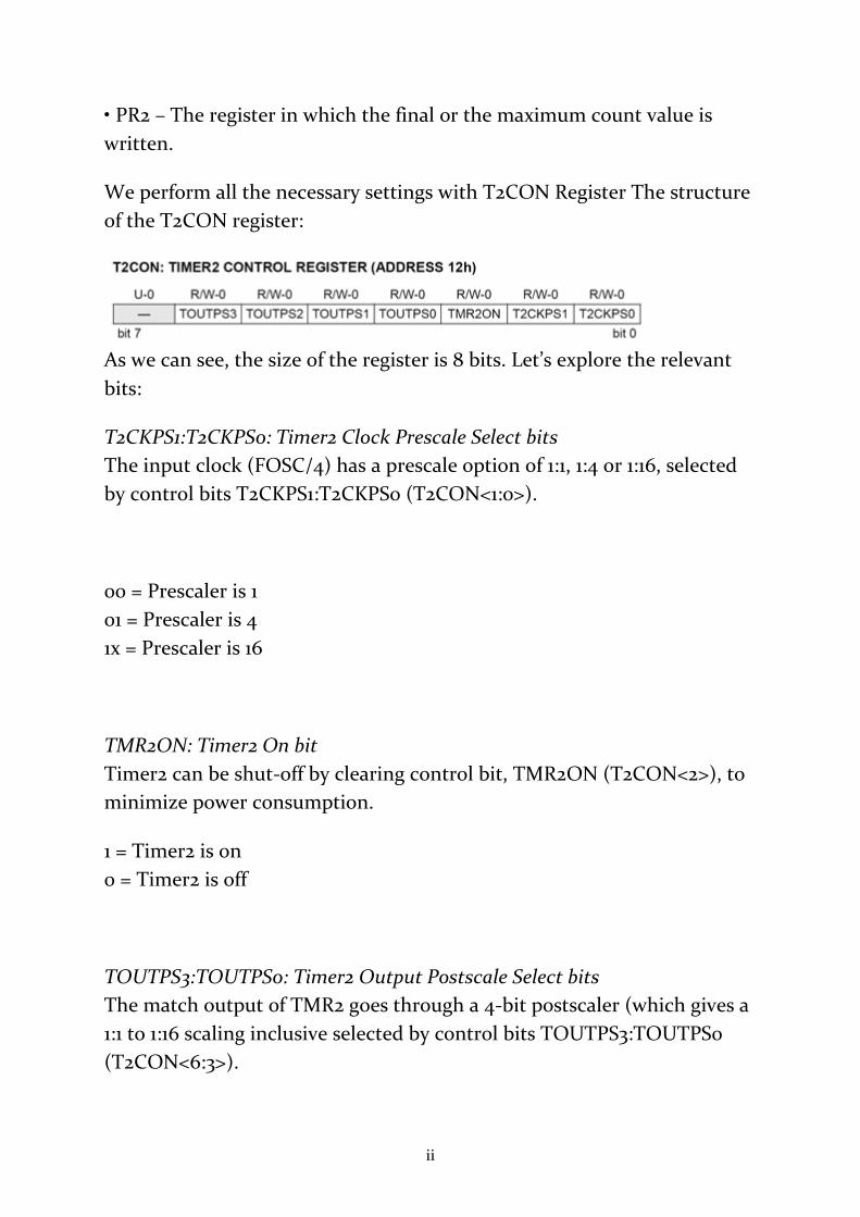
We perform all the necessary settings with T2CON Register The structure
of the T2CON register:
As we can see, the size of the register is 8 bits. Let’s explore the relevant
bits:
T2CKPS1:T2CKPS0: Timer2 Clock Prescale Select bits
The input clock (FOSC/4) has a prescale option of 1:1, 1:4 or 1:16, selected
by control bits T2CKPS1:T2CKPS0 (T2CON<1:0>).
00 = Prescaler is 1
01 = Prescaler is 4
1x = Prescaler is 16
TMR2ON: Timer2 On bit
Timer2 can be shut-off by clearing control bit, TMR2ON (T2CON<2>), to
minimize power consumption.
1 = Timer2 is on
0 = Timer2 is off
TOUTPS3:TOUTPS0: Timer2 Output Postscale Select bits
The match output of TMR2 goes through a 4-bit postscaler (which gives a
1:1 to 1:16 scaling inclusive selected by control bits TOUTPS3:TOUTPS0
(T2CON<6:3>).
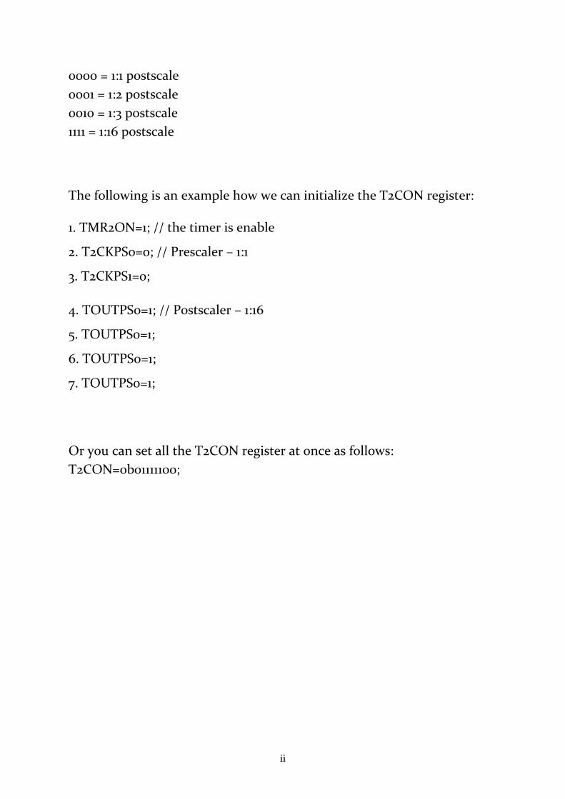
ii
0000 = 1:1 postscale
0001 = 1:2 postscale
0010 = 1:3 postscale
1111 = 1:16 postscale
The following is an example how we can initialize the T2CON register:
1. TMR2ON=1; // the timer is enable
2. T2CKPS0=0; // Prescaler – 1:1
3. T2CKPS1=0;
4. TOUTPS0=1; // Postscaler – 1:16
5. TOUTPS0=1;
6. TOUTPS0=1;
7. TOUTPS0=1;
Or you can set all the T2CON register at once as follows:
T2CON=0b01111100;
ii
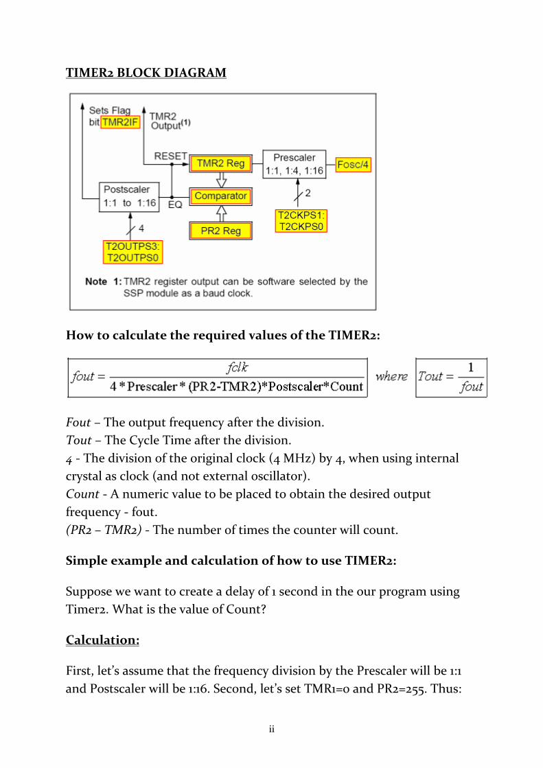
TIMER2 BLOCK DIAGRAM
How to calculate the required values of the TIMER2:
Fout – The output frequency after the division.
Tout – The Cycle Time after the division.
4 - The division of the original clock (4 MHz) by 4, when using internal
crystal as clock (and not external oscillator).
Count - A numeric value to be placed to obtain the desired output
frequency - fout.
(PR2 – TMR2) - The number of times the counter will count.
Simple example and calculation of how to use TIMER2:
Suppose we want to create a delay of 1 second in the our program using
Timer2. What is the value of Count?
Calculation:
First, let’s assume that the frequency division by the Prescaler will be 1:1
and Postscaler will be 1:16. Second, let’s set TMR1=0 and PR2=255. Thus:
ii
Introduction to Serial communication with PIC16F877
microcontroller
In this tutorial we will study the communication component – USART
(Universal Synchronous Asynchronous Receiver Transmitter) located
within the PIC. It is a universal communication component
(Synchronous/Asynchronous), which can be used as transmitter or as
receiver. We will look at:
serial and parallel communications synchronous and asynchronous communications how to enable serial communication - TXSTA and RCSTA registers An example of 8-bit transmission An example of 9-bit transmission how to calculate the value being placed in the SPBRG register USART Transmit and Receive block diagrams Max323 Driver/Receiver the implementation of the PIC serial communication (C program
and a video)
We will show how to set USART in order to allow communication
between PIC to PIC or between PIC to a personal computer. We will start
with the definition of media concepts. There are two options to
differentiate when speaking about transmission of information on the
transmission lines:
serial communication parallel communication
ii
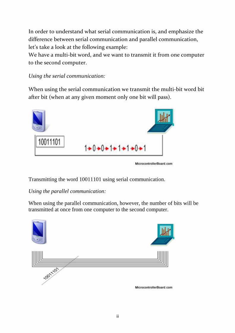
In order to understand what serial communication is, and emphasize the
difference between serial communication and parallel communication,
let’s take a look at the following example:
We have a multi-bit word, and we want to transmit it from one computer
to the second computer.
Using the serial communication:
When using the serial communication we transmit the multi-bit word bit
after bit (when at any given moment only one bit will pass).
Transmitting the word 10011101 using serial communication.
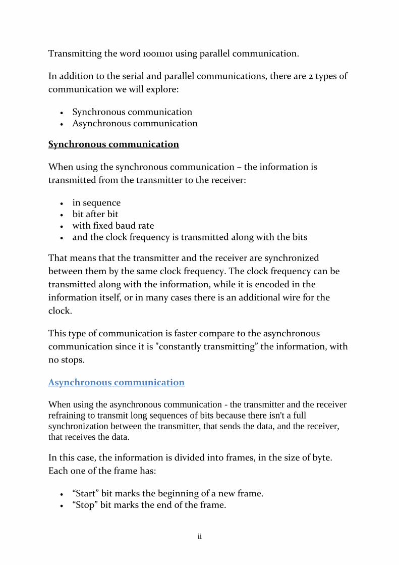
Using the parallel communication:
When using the parallel communication, however, the number of bits will be
transmitted at once from one computer to the second computer.
ii
Transmitting the word 10011101 using parallel communication.
In addition to the serial and parallel communications, there are 2 types of
communication we will explore:
Synchronous communication Asynchronous communication
Synchronous communication
When using the synchronous communication – the information is
transmitted from the transmitter to the receiver:
in sequence bit after bit with fixed baud rate and the clock frequency is transmitted along with the bits
That means that the transmitter and the receiver are synchronized
between them by the same clock frequency. The clock frequency can be
transmitted along with the information, while it is encoded in the
information itself, or in many cases there is an additional wire for the
clock.
This type of communication is faster compare to the asynchronous
communication since it is "constantly transmitting” the information, with
no stops.
Asynchronous communication
When using the asynchronous communication - the transmitter and the receiver
refraining to transmit long sequences of bits because there isn't a full
synchronization between the transmitter, that sends the data, and the receiver,
that receives the data.
In this case, the information is divided into frames, in the size of byte.
Each one of the frame has:
“Start” bit marks the beginning of a new frame. “Stop” bit marks the end of the frame.
ii
Frames of information must not necessarily be transmitted at equal time
space, since they are independent of the clock.
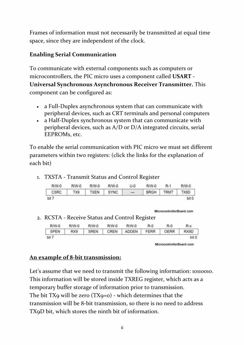
Enabling Serial Communication
To communicate with external components such as computers or
microcontrollers, the PIC micro uses a component called USART -
Universal Synchronous Asynchronous Receiver Transmitter. This
component can be configured as:
a Full-Duplex asynchronous system that can communicate with peripheral devices, such as CRT terminals and personal computers
a Half-Duplex synchronous system that can communicate with peripheral devices, such as A/D or D/A integrated circuits, serial EEPROMs, etc.
To enable the serial communication with PIC micro we must set different
parameters within two registers: (click the links for the explanation of
each bit)
1. TXSTA - Transmit Status and Control Register
2. RCSTA - Receive Status and Control Register
An example of 8-bit transmission:
Let’s assume that we need to transmit the following information: 10110010.
This information will be stored inside TXREG register, which acts as a
temporary buffer storage of information prior to transmission.
The bit TX9 will be zero (TX9=0) - which determines that the
transmission will be 8-bit transmission, so there is no need to address
TX9D bit, which stores the ninth bit of information.
ii
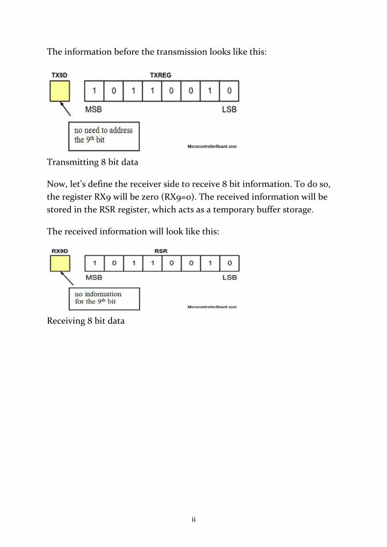
The information before the transmission looks like this:
Transmitting 8 bit data
Now, let’s define the receiver side to receive 8 bit information. To do so,
the register RX9 will be zero (RX9=0). The received information will be
stored in the RSR register, which acts as a temporary buffer storage.
The received information will look like this:
Receiving 8 bit data
ii
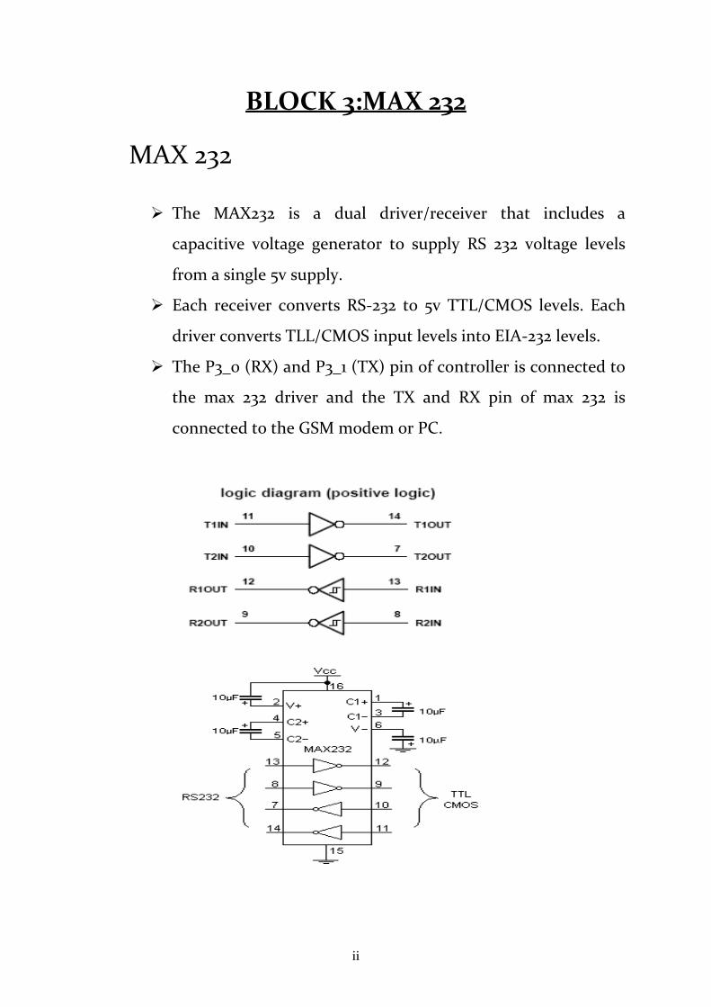
BLOCK 3:MAX 232
MAX 232 The MAX232 is a dual driver/receiver that includes a
capacitive voltage generator to supply RS 232 voltage levels
from a single 5v supply.
Each receiver converts RS-232 to 5v TTL/CMOS levels. Each
driver converts TLL/CMOS input levels into EIA-232 levels.
The P3_0 (RX) and P3_1 (TX) pin of controller is connected to
the max 232 driver and the TX and RX pin of max 232 is
connected to the GSM modem or PC.
ii
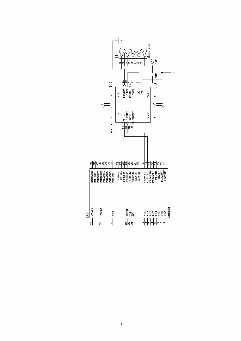
In this circuit the microcontroller transmitter pin is
connected in the MAX232 T2IN pin which converts input 5v
TTL/CMOS level to RS232 level.
Then T2OUT pin is connected to reviver pin of 9 pin D type
serial connector which is directly connected to PC.
In PC the transmitting data is given to R2IN of MAX232
through transmitting pin of 9 pin D type connector which
converts the RS232 level to 5v TTL/CMOS level.
The R2OUT pin is connected to receiver pin of the
microcontroller. Likewise the data is transmitted and received
between the microcontroller and PC or other device vice
versa.
CIRCUIT
ii
ii
BLOCK4 : LCD MODULE
►Introduction
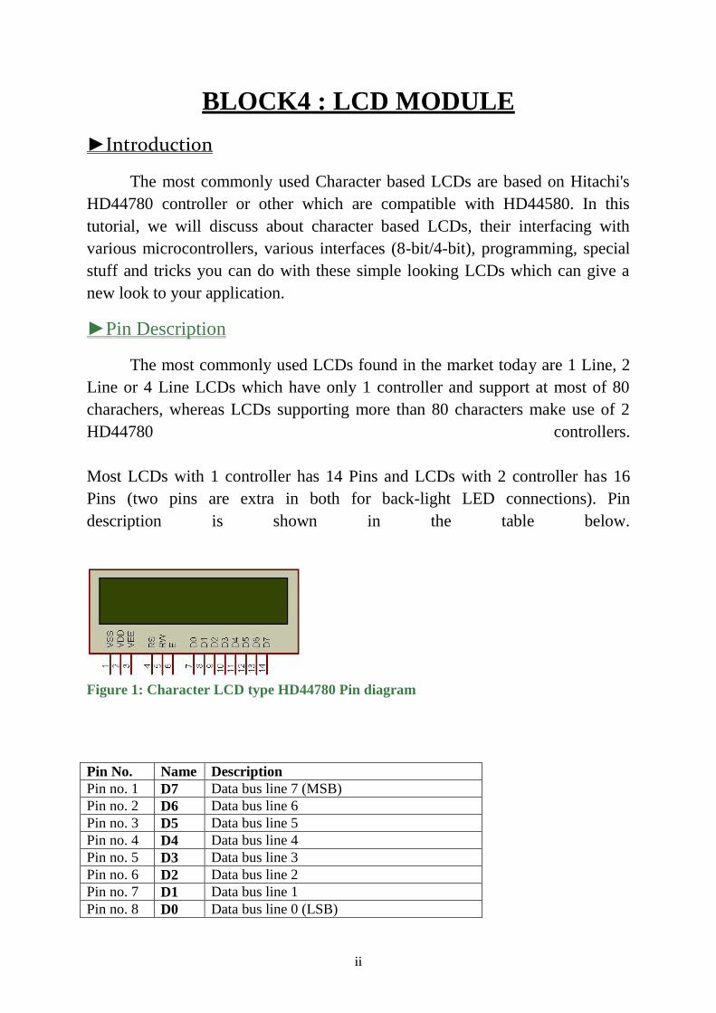
The most commonly used Character based LCDs are based on Hitachi's
HD44780 controller or other which are compatible with HD44580. In this
tutorial, we will discuss about character based LCDs, their interfacing with
various microcontrollers, various interfaces (8-bit/4-bit), programming, special
stuff and tricks you can do with these simple looking LCDs which can give a
new look to your application.
►Pin Description
The most commonly used LCDs found in the market today are 1 Line, 2
Line or 4 Line LCDs which have only 1 controller and support at most of 80
charachers, whereas LCDs supporting more than 80 characters make use of 2
HD44780 controllers.
Most LCDs with 1 controller has 14 Pins and LCDs with 2 controller has 16
Pins (two pins are extra in both for back-light LED connections). Pin
description is shown in the table below.
Figure 1: Character LCD type HD44780 Pin diagram
Pin No. Name Description
Pin no. 1 D7 Data bus line 7 (MSB)
Pin no. 2 D6 Data bus line 6
Pin no. 3 D5 Data bus line 5
Pin no. 4 D4 Data bus line 4
Pin no. 5 D3 Data bus line 3
Pin no. 6 D2 Data bus line 2
Pin no. 7 D1 Data bus line 1
Pin no. 8 D0 Data bus line 0 (LSB)
ii
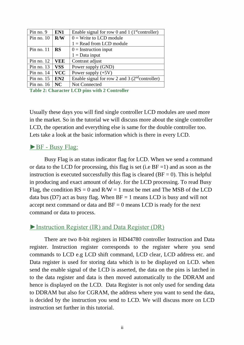
Pin no. 9 EN1 Enable signal for row 0 and 1 (1stcontroller)
Pin no. 10 R/W 0 = Write to LCD module
1 = Read from LCD module
Pin no. 11 RS 0 = Instruction input
1 = Data input
Pin no. 12 VEE Contrast adjust
Pin no. 13 VSS Power supply (GND)
Pin no. 14 VCC Power supply (+5V)
Pin no. 15 EN2 Enable signal for row 2 and 3 (2ndcontroller)
Pin no. 16 NC Not Connected
Table 2: Character LCD pins with 2 Controller
Usually these days you will find single controller LCD modules are used more
in the market. So in the tutorial we will discuss more about the single controller
LCD, the operation and everything else is same for the double controller too.
Lets take a look at the basic information which is there in every LCD.
►BF - Busy Flag:
Busy Flag is an status indicator flag for LCD. When we send a command
or data to the LCD for processing, this flag is set (i.e BF =1) and as soon as the
instruction is executed successfully this flag is cleared (BF = 0). This is helpful
in producing and exact amount of delay. for the LCD processing. To read Busy
Flag, the condition RS = 0 and R/W = 1 must be met and The MSB of the LCD
data bus (D7) act as busy flag. When BF = 1 means LCD is busy and will not
accept next command or data and BF = 0 means LCD is ready for the next
command or data to process.
►Instruction Register (IR) and Data Register (DR)
There are two 8-bit registers in HD44780 controller Instruction and Data
register. Instruction register corresponds to the register where you send
commands to LCD e.g LCD shift command, LCD clear, LCD address etc. and
Data register is used for storing data which is to be displayed on LCD. when
send the enable signal of the LCD is asserted, the data on the pins is latched in
to the data register and data is then moved automatically to the DDRAM and
hence is displayed on the LCD. Data Register is not only used for sending data
to DDRAM but also for CGRAM, the address where you want to send the data,
is decided by the instruction you send to LCD. We will discuss more on LCD
instruction set further in this tutorial.
ii
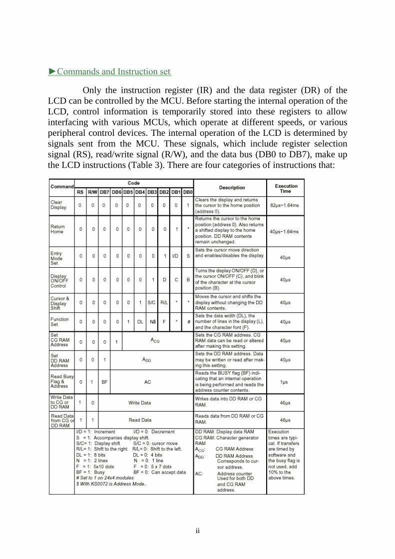
►Commands and Instruction set
Only the instruction register (IR) and the data register (DR) of the
LCD can be controlled by the MCU. Before starting the internal operation of the
LCD, control information is temporarily stored into these registers to allow
interfacing with various MCUs, which operate at different speeds, or various
peripheral control devices. The internal operation of the LCD is determined by
signals sent from the MCU. These signals, which include register selection
signal (RS), read/write signal (R/W), and the data bus (DB0 to DB7), make up
the LCD instructions (Table 3). There are four categories of instructions that:
ii
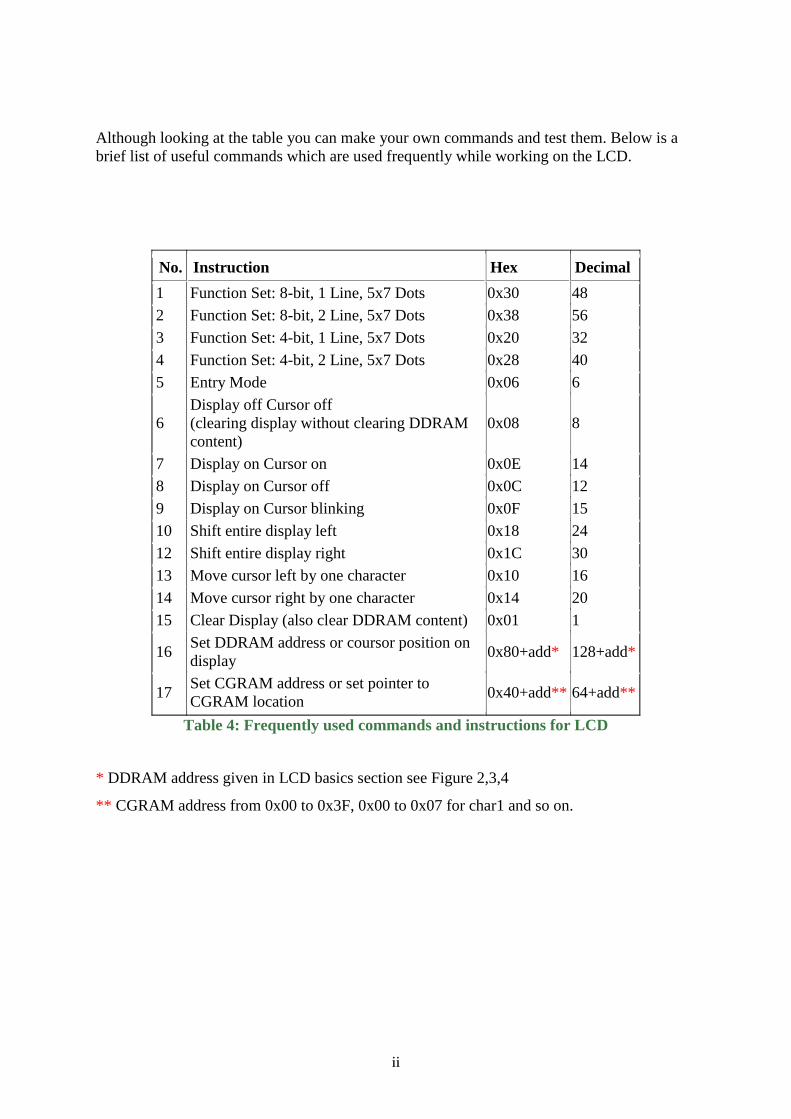
Although looking at the table you can make your own commands and test them. Below is a
brief list of useful commands which are used frequently while working on the LCD.
No. Instruction Hex Decimal
1 Function Set: 8-bit, 1 Line, 5x7 Dots 0x30 48
2 Function Set: 8-bit, 2 Line, 5x7 Dots 0x38 56
3 Function Set: 4-bit, 1 Line, 5x7 Dots 0x20 32
4 Function Set: 4-bit, 2 Line, 5x7 Dots 0x28 40
5 Entry Mode 0x06 6
6
Display off Cursor off
(clearing display without clearing DDRAM
content)
0x08 8
7 Display on Cursor on 0x0E 14
8 Display on Cursor off 0x0C 12
9 Display on Cursor blinking 0x0F 15
10 Shift entire display left 0x18 24
12 Shift entire display right 0x1C 30
13 Move cursor left by one character 0x10 16
14 Move cursor right by one character 0x14 20
15 Clear Display (also clear DDRAM content) 0x01 1
16 Set DDRAM address or coursor position on
display 0x80+add* 128+add*
17 Set CGRAM address or set pointer to
CGRAM location 0x40+add** 64+add**
Table 4: Frequently used commands and instructions for LCD
* DDRAM address given in LCD basics section see Figure 2,3,4
** CGRAM address from 0x00 to 0x3F, 0x00 to 0x07 for char1 and so on.

ii
BLOCK 5: APR 9600 VOICE IC
APR9600 is a low-cost high performance sound
record/replay IC incorporating flash analogue storage
technique. Recorded sound is retained even after power
supply is removed from the module.
The replayed sound exhibits high quality with a low noise
level. Sampling rate for a 60 second recording period is
4.2 kHz that gives a sound record/replay bandwidth of
20Hz to 2.1 kHz.
However, by changing an oscillation resistor, a sampling
rate as high as 8.0 kHz can be achieved. This shortens the
total length of sound recording to 32 seconds.
Total sound recording time can be varied from 32 seconds
to 60 seconds by changing the value of a single resistor.
The IC can operate in one of two modes: serial mode and
parallel mode. In serial access mode, sound can be
recorded in 256 sections.
In parallel access mode, sound can be recorded in 2, 4 or 8
sections. The IC can be controlled simply using push
button keys. It is also possible to control the IC using
external digital circuitry such as micro-controllers and
computers.
ii
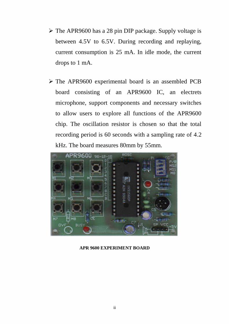
The APR9600 has a 28 pin DIP package. Supply voltage is
between 4.5V to 6.5V. During recording and replaying,
current consumption is 25 mA. In idle mode, the current
drops to 1 mA.
The APR9600 experimental board is an assembled PCB
board consisting of an APR9600 IC, an electrets
microphone, support components and necessary switches
to allow users to explore all functions of the APR9600
chip. The oscillation resistor is chosen so that the total
recording period is 60 seconds with a sampling rate of 4.2
kHz. The board measures 80mm by 55mm.
APR 9600 EXPERIMENT BOARD
ii
APR 9600
Pin-out of the APR9600 is given in Figure 1. A typical connection
of the chip is given in Figure 2 (This is the circuit diagram of the
module).
During sound recording, sound is picked up by the microphone. A
microphone pre-amplifier amplifies the voltage signal from the
microphone. An AGC circuit is included in the pre-amplifier, the
extent of which is controlled by an external capacitor and resistor.
If the voltage level of a sound signal is around 100 mV peak to-
peak, the signal can be fed directly into the IC through ANA IN pin
(pin 20). The sound signal passes through a filter and a sampling
and hold circuit. The analogue voltage is then written into non-
volatile flash analogue RAMs. It has a 28 pin DIP package. Supply
voltage is between 4.5V to 6.5V.
During recording and replaying, current consumption is 25 mA. In
idle mode, the current drops to 1 mA.
ii
ii
TYPICAL CONNECTION OF APR9600
APR9600 MODULE
The circuit diagram of the module is shown in Figure 2. The module consists of an
APR9600 chip, an electrets microphone, support components, a mode selection
switch (-RE, MSEL1, MSEL2 and – M8) and 9 keys (-M1 to –M8 and CE). The
oscillation resistor is chosen so that the total recording period is 60 seconds with a
sampling rate of 4.2 kHz.
Users can change the value of the ROSC to obtain other sampling frequencies. It
should be noted that if the sampling rate is increased, the length of recording time is
decreased. Table 3 gives the details. An 8-16 Ohm speaker is to be used with the
module. Users can select different modes using the mode selection switch.
The module is measured 80mm´55mm. Connection points (0-8, C and B) can connect
to other switches or external digital circuits. In this cased, on-board keys M1 to M8
and CE are by-passed.
ii
Application tips
1. Use a good quality 8 Ohm speaker with a cavity such as speakers for
computer sound systems. Do not use a bare speaker which gives you degraded
sound.
2. For better sound replay quality, speak with a distance to the on-board
microphone and speak clearly. Also keep the background noise as low as
possible.
3. For even better sound replay quality, use microphone input or Audio Line In
input. If Audio Line In is used, the amplitude of input signal should be < 100
mV p-p.
ii
BLOCK 6: MPLAB COMPILER
ABOUT MPLAB COMPILER:
The MPLAB X IDE is the new graphical, integrated debugging tool set for all of
Microchip’s more than 800 8-bit, 16-bit and 32-bit MCUs and digital signal
controllers, and memory devices.
It includes a feature-rich editor, source-level debugger, project manager, software
simulator, and supports Microchip’s popular hardware tools, such as the MPLAB ICD
3 in-circuit debugger, PICkit™ 3, and MPLAB PM3 programmer.
Based on the open-source NetBeans platform, MPLAB X runs on Windows® OS,
MAC® OS and Linux, supports many third-party tools, and is compatible with many
NetBeans plug-ins.
MPLAB IDE v8
What is MPLAB IDE?
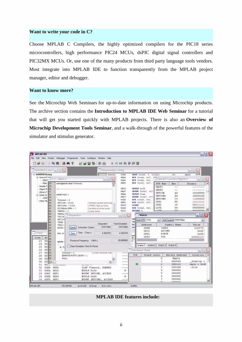
MPLAB Integrated Development Environment (IDE) is a free, integrated toolset for the
development of embedded applications employing Microchip's PIC® and
dsPIC® microcontrollers. MPLAB IDE runs as a 32-bit application on MS Windows®, is easy
to use and includes a host of free software components for fast application development and
super-charged debugging. MPLAB IDE also serves as a single, unified graphical user
interface for additional Microchip and third party software and hardware development tools.
Moving between tools is a snap, and upgrading from the free software simulator to hardware
debug and programming tools is done in a flash because MPLAB IDE has the same user
interface for all tools.
Don't know where to start?
Download MPLAB IDE and use the tutorial in the MPLAB IDE User’s Guide at the bottom
of this page to explore how easy it is to create an application. Write assembly code, build and
assemble your project with MPLAB's wizards, then test your code with the built-in simulator
and debugger. When you are ready to test your own application, select one of our low-cost
debugger/programmers to program a device and analyze your hardware.
ii
Want to write your code in C?
Choose MPLAB C Compilers, the highly optimized compilers for the PIC18 series
microcontrollers, high performance PIC24 MCUs, dsPIC digital signal controllers and
PIC32MX MCUs. Or, use one of the many products from third party language tools vendors.
Most integrate into MPLAB IDE to function transparently from the MPLAB project
manager, editor and debugger.
Want to know more?
See the Microchip Web Seminars for up-to-date information on using Microchip products.
The archive section contains the Introduction to MPLAB IDE Web Seminar for a tutorial
that will get you started quickly with MPLAB projects. There is also an Overview of
Microchip Development Tools Seminar, and a walk-through of the powerful features of the
simulator and stimulus generator.
MPLAB IDE features include:
ii
Flexible customizable programmer's text
editor
Free components
Fully integrated debugging with
right mouse click menus for
breakpoints, trace and editor
functions
Tabbed editor option or separate
source windows
Recordable macros
Context sensitive color
highlighting for assembly, C and
BASIC code readability
Mouse over variable to instantly
evaluate the contents of variables
and registers
Set breakpoints and
tracepoints directly in editor to
instantly make changes and evaluate
their effects
Graphical project manager
Version control support for MS
Source Safe, CVS, PVCS,
Subversion
Programmer’s text editor
MPLAB SIM, high speed software
simulator for PIC and dsPIC devices with
peripheral simulation, complex stimulus
injection and register logging
Full featured debugger
MPASM™ and MPLINK for PIC MCUs
and dsPIC DSC devices
HI-TECH C PRO for PIC10/12/16 MCU
Families running in lite mode
CCS PCB C Compiler
Labcenter Electronic’s Proteus
VSM spice simulator
Many Powerful Plug-Ins including
○ AN851 Bootloader programmer
○ AN901 BLDC Motor Control Interface
○ AN908 ACIM Tuning Interface
○ KeeLoq support
○ Real Time Data Monitor and Control
Simple, powerful source level debugging Built in support for hardware and add-on
components
Auto alignment of
breakpoints after source code
modification
Mouse-over variable inspection
Drag and drop variables to watch
windows
Watch variables, structures and
MPLAB C Compilers (free student
editions available for download)
MPLAB REAL ICE™ in-circuit emulator
MPLAB ICD 2 and MPLAB ICD 3 in-
circuit debuggers and engineering
programmers for selected Flash devices
PICkit 2 and PICkit 3 Debug
ii
arrays
Mixed source code/disassembly
view
Stack symbolic return label
display
Automatic single-step "animate"
feature
Pass counts and break on PIC18F,
PIC24 and dsPIC file register R/W
for MPLAB ICD 2
Step-Out-Of function
Custom hot keys
Powerful simulator stimulus
generator
Trace to source correlation to
compare real time data collected
with original source code and
comments
Express economy debug/programmers
PICSTART Plus development
programmer
MPLAB PM3 device programmer
Third Party tools, including HI-TECH,
IAR, Byte Craft, B. Knudsen, CCS,
Micrium, microEngineering Labs,
Labcenter, MATLAB, Segger
A host of low cost starter boards,
demonstration and evaluation kits
ii
SYSTEM SOFTWARE
ii
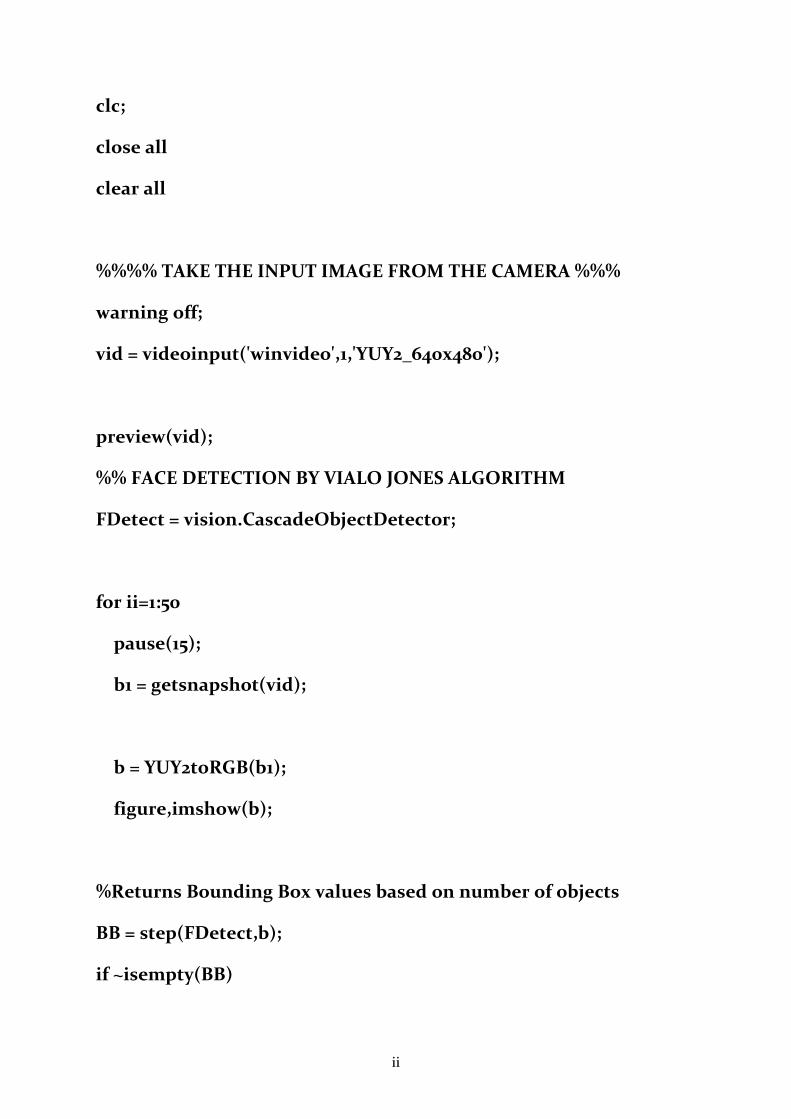
clc;
close all
clear all
%%%% TAKE THE INPUT IMAGE FROM THE CAMERA %%%
warning off;
vid = videoinput('winvideo',1,'YUY2_640x480');
preview(vid);
%% FACE DETECTION BY VIALO JONES ALGORITHM
FDetect = vision.CascadeObjectDetector;
for ii=1:50
pause(15);
b1 = getsnapshot(vid);
b = YUY2toRGB(b1);
figure,imshow(b);
%Returns Bounding Box values based on number of objects
BB = step(FDetect,b);
if ~isempty(BB)
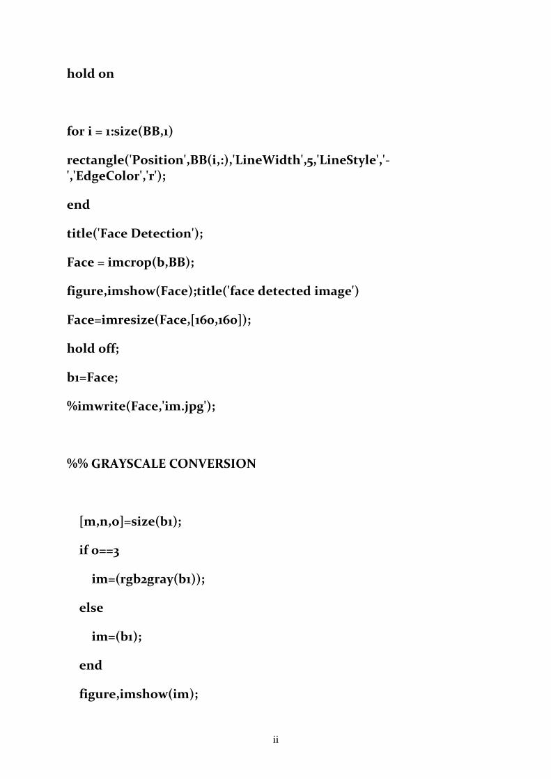
ii
hold on
for i = 1:size(BB,1)
rectangle('Position',BB(i,:),'LineWidth',5,'LineStyle','-','EdgeColor','r');
end
title('Face Detection');
Face = imcrop(b,BB);
figure,imshow(Face);title('face detected image')
Face=imresize(Face,[160,160]);
hold off;
b1=Face;
%imwrite(Face,'im.jpg');
%% GRAYSCALE CONVERSION
[m,n,o]=size(b1);
if o==3
im=(rgb2gray(b1));
else
im=(b1);
end
figure,imshow(im);
ii
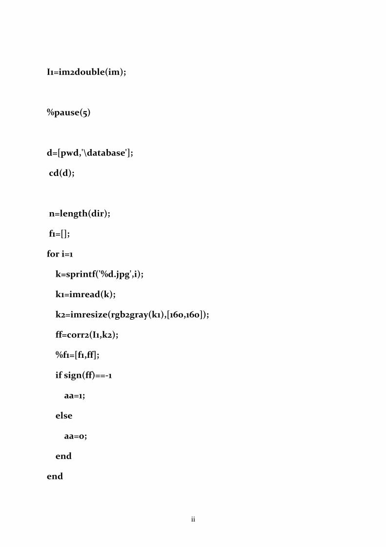
I1=im2double(im);
%pause(5)
d=[pwd,'\database'];
cd(d);
n=length(dir);
f1=[];
for i=1
k=sprintf('%d.jpg',i);
k1=imread(k);
k2=imresize(rgb2gray(k1),[160,160]);
ff=corr2(I1,k2);
%f1=[f1,ff];
if sign(ff)==-1
aa=1;
else
aa=0;
end
end
ii
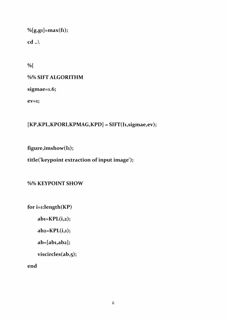
%[g,g1]=max(f1);
cd ..\
%{
%% SIFT ALGORITHM
sigmae=1.6;
ev=1;
[KP,KPL,KPORI,KPMAG,KPD] = SIFT(I1,sigmae,ev);
figure,imshow(I1);
title('keypoint extraction of input image');
%% KEYPOINT SHOW
for i=1:length(KP)
ab1=KPL(i,2);
ab2=KPL(i,1);
ab=[ab1,ab2];
viscircles(ab,5);
end
ii
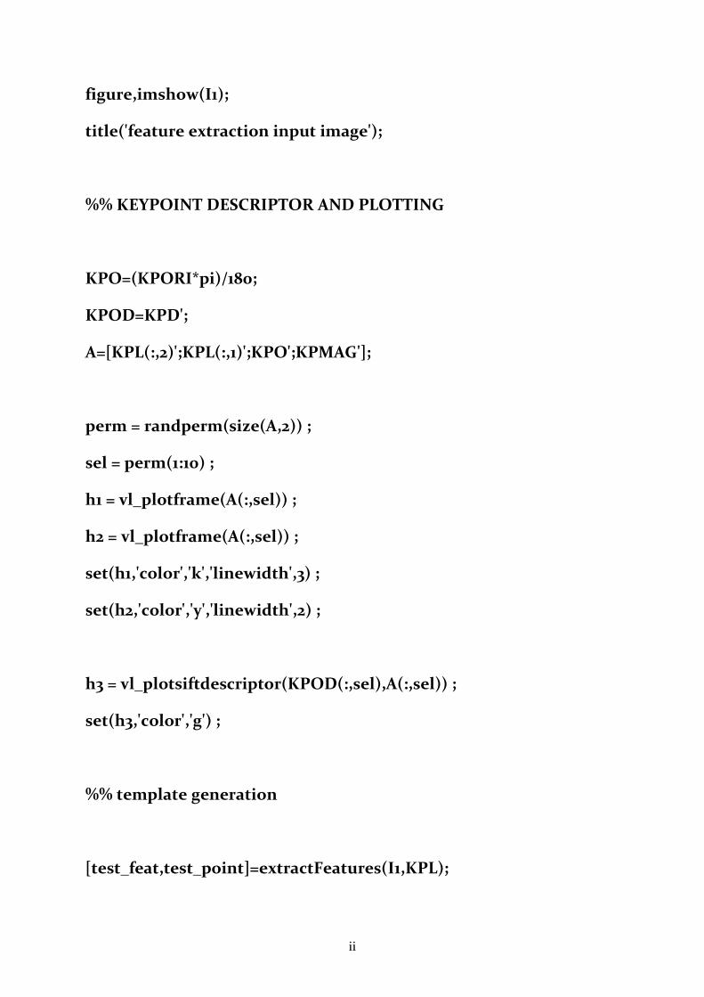
figure,imshow(I1);
title('feature extraction input image');
%% KEYPOINT DESCRIPTOR AND PLOTTING
KPO=(KPORI*pi)/180;
KPOD=KPD';
A=[KPL(:,2)';KPL(:,1)';KPO';KPMAG'];
perm = randperm(size(A,2)) ;
sel = perm(1:10) ;
h1 = vl_plotframe(A(:,sel)) ;
h2 = vl_plotframe(A(:,sel)) ;
set(h1,'color','k','linewidth',3) ;
set(h2,'color','y','linewidth',2) ;
h3 = vl_plotsiftdescriptor(KPOD(:,sel),A(:,sel)) ;
set(h3,'color','g') ;
%% template generation
[test_feat,test_point]=extractFeatures(I1,KPL);
ii
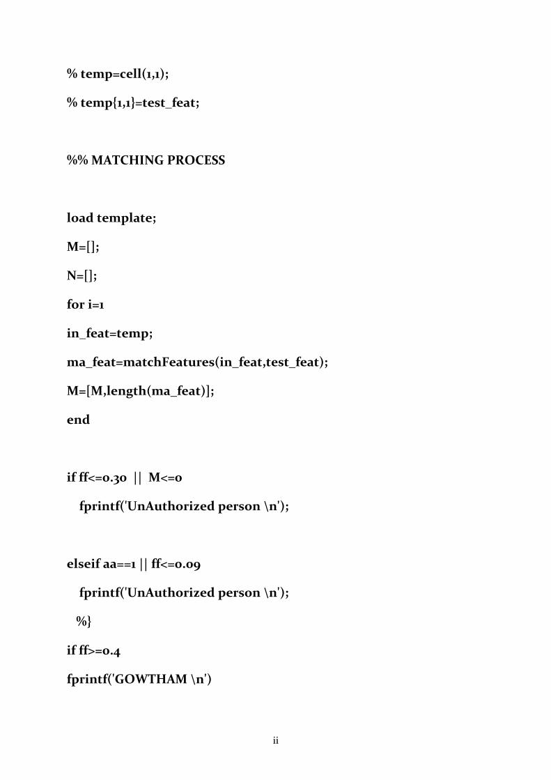
% temp=cell(1,1);
% temp{1,1}=test_feat;
%% MATCHING PROCESS
load template;
M=[];
N=[];
for i=1
in_feat=temp;
ma_feat=matchFeatures(in_feat,test_feat);
M=[M,length(ma_feat)];
end
if ff<=0.30 || M<=0
fprintf('UnAuthorized person \n');
elseif aa==1 || ff<=0.09
fprintf('UnAuthorized person \n');
%}
if ff>=0.4
fprintf('GOWTHAM \n')
ii
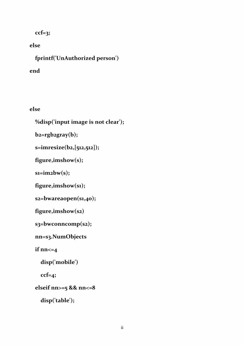
ccf=3;
else
fprintf('UnAuthorized person')
end
else
%disp('input image is not clear');
b2=rgb2gray(b);
s=imresize(b2,[512,512]);
figure,imshow(s);
s1=im2bw(s);
figure,imshow(s1);
s2=bwareaopen(s1,40);
figure,imshow(s2)
s3=bwconncomp(s2);
nn=s3.NumObjects
if nn<=4
disp('mobile')
ccf=4;
elseif nn>=5 && nn<=8
disp('table');
ii
ccf=2;
elseif nn>=9 && nn<=20
disp('chair');
ccf=1;
else
disp('unwanted content');
end
end
%% HARDWARE
instrumentObjects=instrfind; % don't pass it anything - find all of them.
delete(instrumentObjects)
a=serial('COM1','BaudRate',9600);
fopen(a);
if ccf==1
fprintf(a,'1');
elseif ccf==2
fprintf(a,'2');
elseif ccf==3
fprintf(a,'3');

ii
elseif ccf==4
fprintf(a,'4');
end
fclose(a);
pause(2)
close all;
end
delete(vid);

ii
CONCLUSION
The aim of this project work undertaken in our polytechnic is to improve our practical knowledge and to implement our creativity in scientific and technical way.
The project work teaches us, how the work can be done collectively with proper understanding among the members of the team.
We have successfully completed the project. We have made this project entirely different from the rest. Since concepts involved is entirely different that based blind person to find the person or way without anyone help with the use of pic micro controller and the web camera, which makes our project a unique.
By doing this project we gained knowledge of pic micro controller based systems and knew many things related to our project`
In this way, we can conclude that this project idea will take a major role in our science world to give a confidential survive for a blind person.

ii
Related Documents