Gowin MIPI D-PHY RX TX Advance IP User Guide IPUG948-1.11E, 07/09/2021

Welcome message from author
This document is posted to help you gain knowledge. Please leave a comment to let me know what you think about it! Share it to your friends and learn new things together.
Transcript
Gowin MIPI D-PHY RX TX Advance IP
User Guide
IPUG948-1.11E, 07/09/2021

Copyright © 2021 Guangdong Gowin Semiconductor Corporation. All Rights Reserved.
, , Gowin, and GOWINSEMI are trademarks of Guangdong Gowin
Semiconductor Corporation and are registered in China, the U.S. Patent and Trademark
Office, and other countries. All other words and logos identified as trademarks or service
marks are the property of their respective holders. No part of this document may be
reproduced or transmitted in any form or by any denotes, electronic, mechanical,
photocopying, recording or otherwise, without the prior written consent of GOWINSEMI.
Disclaimer
GOWINSEMI assumes no liability and provides no warranty (either expressed or implied)
and is not responsible for any damage incurred to your hardware, software, data, or
property resulting from usage of the materials or intellectual property except as outlined in
the GOWINSEMI Terms and Conditions of Sale. All information in this document should be
treated as preliminary. GOWINSEMI may make changes to this document at any time
without prior notice. Anyone relying on this documentation should contact GOWINSEMI for
the current documentation and errata.
Revision History
Date Version Description
09/01/2020 1.0E Initial version published.
04/27/2021 1.1E The description of D-PHY RX Ports revised.
07/09/2021 1.11E The supported device info. improved.
The Appendix A MIPI D-PHY Data Rates added.
Contents
IPUG948-1.11E i
Contents
Contents ............................................................................................................... i
List of Figures .................................................................................................... iii
List of Tables ...................................................................................................... iv
1 About This Guide ............................................................................................. 1
1.1 Purpose .............................................................................................................................. 1
1.2 Related Documents ............................................................................................................ 1
1.3 Terminology and Abbreviations ........................................................................................... 1
1.4 Support and Feedback ....................................................................................................... 2
2 Overview ........................................................................................................... 3
2.1 Introduction to MIPI D-PHY RX/TX Advance IP ................................................................. 3
2.2 MIPI D-PHY ........................................................................................................................ 4
3 Features and Performance ............................................................................. 5
3.1 Features .............................................................................................................................. 5
3.2 Max. Frequency .................................................................................................................. 5
3.3 Latency ............................................................................................................................... 5
3.4 Resource Utilization ............................................................................................................ 6
3.5 Devices Supported ............................................................................................................. 7
4 Functional Description .................................................................................... 8
4.1 MIPI D-PHY RX Advance Structure and Function .............................................................. 8
4.2 MIPI D-PHY TX Advance Structure and Function ............................................................ 10
4.3 MIPI IO .............................................................................................................................. 13
5 Port Description ............................................................................................. 15
5.1 MIPI D-PHY RX Advance Ports ........................................................................................ 15
5.2 MIPI D-PHY TX Advance Ports ........................................................................................ 17
Contents
IPUG948-1.11E ii
6 Timing Description ........................................................................................ 19
6.1 RX Input Signal Timing ..................................................................................................... 19
6.2 TX Input Signal Timing ...................................................................................................... 20
7 Configuration and Generation ...................................................................... 23
7.1 MIPI D-PHY RX Advance Configuration ........................................................................... 23
7.2 MIPI D-PHY TX Advance Configuration ........................................................................... 26
List of Figures
IPUG948-1.11E iii
List of Figures
Figure 2-1 MIPI D-PHY Structure Diagram ........................................................................................ 4
Figure 4-1 Interface Implementation in HS Mode and LP Mode ....................................................... 9
Figure 4-2 Interface Implementation in HS Mode and LP Mode (ELVDS Adopted in HS Mode) ...... 11
Figure 4-3 Interface Implementation in HS Mode and LP Mode (TLVDS Adopted in HS Mode) ...... 12
Figure 4-4 MIPI IP Ports in MIPI IO Mode ......................................................................................... 13
Figure 4-5 MIPI IP Ports in MIPI IO Mode (External Termination Resistor Required) ....................... 14
Figure 6-1 Input Signal Timing of MIPI D-PHY RX Advance in HS 1:8 Mode ................................... 20
Figure 6-2 Input Signal Timing of MIPI D-PHY TX Advance in HS 1:8 Mode .................................... 21
Figure 6-3 Input Signal Timing of MIPI D-PHY TX Advance in HS 1:16 Mode .................................. 21
Figure 7-1 MIPI D-PHY RX Advance Configuration ........................................................................... 24
Figure 7-2 MIPI D-PHY TX Advance Configuration ........................................................................... 26
List of Tables
IPUG948-1.11E iv
List of Tables
Table 1-1 Terminology and Abbreviations .......................................................................................... 2
Table 2-1 MIPI D-PHY RX Advance and TX Advance IP ................................................................... 3
Table 3-1 D-PHY TX/RX Advance Latency ........................................................................................ 6
Table 3-2 MIPI D-PHY RX Advance Resource Utilization.................................................................. 6
Table 3-3 MIPI D-PHY TX Advance Resource Utilization .................................................................. 6
Table 3-4 MIPI D-PHY RX Advance Devices Supported ................................................................... 7
Table 3-5 MIPI D-PHY TX Advance Devices Supported .................................................................... 7
Table 5-1 D-PHY RX Advance I/O Ports ............................................................................................ 15
Table 5-2 D-PHY TX Advance I/O Ports ............................................................................................ 17
Table 7-1 MIPI D-PHY RX Advance Options ..................................................................................... 24
Table 7-2 MIPI D-PHY TX Advance Options ...................................................................................... 26
Table A-1 MIPI D-PHY Data Rates (LittleBee®
Family) ...................................................................... 29
Table A-2 MIPI D-PHY Data Rates (Arora Family) ............................................................................. 30
1 About This Guide 1.1 Purpose
IPUG948-1.11E 1(30)
1 About This Guide
1.1 Purpose
The purpose of this Gowin MIPI D-PHY RX/TX Advance IP User Guide
is to help you to quickly learn the features and usage of Gowin MIPI D-PHY
RX/TX Advance IP by providing the descriptions of the functions, features,
ports, timing, configuration, and reference design, etc.
1.2 Related Documents
The latest user guides are available on the GOWINSEMI Website. You
can find the related documents at http://www.gowinsemi.com:
1. DS100, GW1N series of FPGA Products Data Sheet
2. DS821, GW1NS series of FPGA Products Data Sheet
3. DS117, GW1NR series of FPGA Products Data Sheet
4. DS861, GW1NSR series of FPGA Products Data Sheet
5. DS102, GW2A series of FPGA Products Data Sheet
6. DS226, GW2AR series of FPGA Products Data Sheet
7. SUG100, Gowin Software User Guide
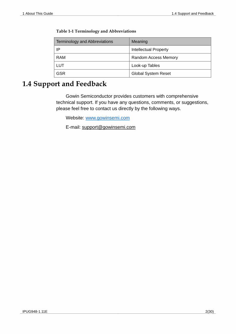
1.3 Terminology and Abbreviations
The terminology and abbreviations used in this manual are as shown
in Table 1-1.
1 About This Guide 1.4 Support and Feedback
IPUG948-1.11E 2(30)
Table 1-1 Terminology and Abbreviations
Terminology and Abbreviations Meaning
IP Intellectual Property
RAM Random Access Memory
LUT Look-up Tables
GSR Global System Reset
1.4 Support and Feedback
Gowin Semiconductor provides customers with comprehensive
technical support. If you have any questions, comments, or suggestions,
please feel free to contact us directly by the following ways.
Website: www.gowinsemi.com
E-mail: [email protected]
2 Overview 2.1 Introduction to MIPI D-PHY RX/TX Advance IP
IPUG948-1.11E 3(30)
2 Overview
2.1 Introduction to MIPI D-PHY RX/TX Advance IP
Gowin MIPI D-PHY TX/RX Advance IP applies to the display serial
interface (DSI) and the camera serial interface (CSI). It aims to receive and
send images or video data. MIPI D-PHY provides a physical layer
definition.
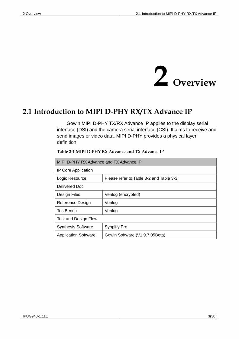
Table 2-1 MIPI D-PHY RX Advance and TX Advance IP
MIPI D-PHY RX Advance and TX Advance IP
IP Core Application
Logic Resource Please refer to Table 3-2 and Table 3-3.
Delivered Doc.
Design Files Verilog (encrypted)
Reference Design Verilog
TestBench Verilog
Test and Design Flow
Synthesis Software Synplify Pro
Application Software Gowin Software (V1.9.7.05Beta)
2 Overview 2.2 MIPI D-PHY
IPUG948-1.11E 4(30)
2.2 MIPI D-PHY
The Mobile Industry Processor Interface (MIPI) is an interface
standard for mobile devices. MIPI D-PHY provides a physical definition for
DSI and CSI and describes the physical layer interface protocols of source
synchronous, high speed, and low power. In accordance with application
requirements, MIPI D-PHY Advance includes RX and TX, which are used
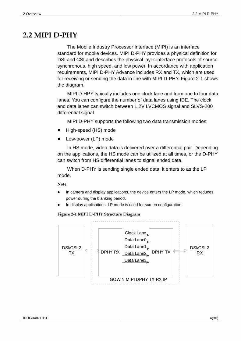
for receiving or sending the data in line with MIPI D-PHY. Figure 2-1 shows
the diagram.
MIPI D-HPY typically includes one clock lane and from one to four data
lanes. You can configure the number of data lanes using IDE. The clock
and data lanes can switch between 1.2V LVCMOS signal and SLVS-200
differential signal.
MIPI D-PHY supports the following two data transmission modes:
High-speed (HS) mode
Low-power (LP) mode
In HS mode, video data is delivered over a differential pair. Depending
on the applications, the HS mode can be utilized at all times, or the D-PHY
can switch from HS differential lanes to signal ended data.
When D-PHY is sending single ended data, it enters to as the LP
mode.
Note!
In camera and display applications, the device enters the LP mode, which reduces
power during the blanking period.
In display applications, LP mode is used for screen configuration.
Figure 2-1 MIPI D-PHY Structure Diagram
DSI/CSI-2
TX DPHY RX DPHY TXDSI/CSI-2
RX
Clock Lane
Data Lane0
Data Lane1
Data Lane2
Data Lane3
GOWIN MIPI DPHY TX RX IP
3 Features and Performance 3.1 Features
IPUG948-1.11E 5(30)
3 Features and Performance
3.1 Features
In line with MIPI Alliance Standard for D-PHY Specification, version
1.1.
Supports the RX and TX Interfaces of MIPI CSI2 and DSI
Supports unidirectional High-speed (HS) mode.
Supports bidirectional Low-power operation mode.
Supports serial high-speed data conversion
Supports MIPI D-PHY TX 8:1 mode and 16:1 mode.
Supports MIPI D-PHY RX 1:8 mode and 1:16 mode.
Supports IO Types of ELVDS, TLVDS, and MIPI IO.
The line rate of the single lane TX supports the range: 80Mb/s ~
1500Mb/s.
The line rate of the single lane RX supports the range: 80Mb/s ~
1200Mb/s.
Data transmission in LP mode is at a speed of 10Mb/s.
3.2 Max. Frequency
The max. frequency of MIPI D-PHY is mainly determined by the line
rate and the speed grade of the devices.
3.3 Latency
D-PHY TX Latency is the time from inputting the data_in (8-bit/16-bit
parallel data) to outputting HS_DATA.
D-PHY RX Latency is the time from inputting the HS_DATA SOT
(start-of-transmission) to outputting data_out (8-bit/16-bit parallel data).
3 Features and Performance 3.4 Resource Utilization
IPUG948-1.11E 6(30)
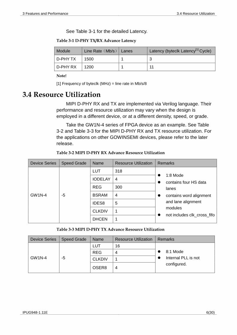
See Table 3-1 for the detailed Latency.
Table 3-1 D-PHY TX/RX Advance Latency
Module Line Rate(Mb/s) Lanes Latency (byteclk Latency[1]
Cycle)
D-PHY TX 1500 1 3
D-PHY RX 1200 1 11
Note!
[1] Frequency of byteclk (MHz) = line rate in Mb/s/8
3.4 Resource Utilization MIPI D-PHY RX and TX are implemented via Verilog language. Their
performance and resource utilization may vary when the design is
employed in a different device, or at a different density, speed, or grade.
Take the GW1N-4 series of FPGA device as an example. See Table
3-2 and Table 3-3 for the MIPI D-PHY RX and TX resource utilization. For
the applications on other GOWINSEMI devices, please refer to the later
release.
Table 3-2 MIPI D-PHY RX Advance Resource Utilization
Device Series Speed Grade Name Resource Utilization Remarks
GW1N-4 -5
LUT 318 1:8 Mode
contains four HS data
lanes
contains word alignment
and lane alignment
modules
not includes clk_cross_fifo
IODELAY 4
REG 300
BSRAM 4
IDES8 5
CLKDIV 1
DHCEN 1
Table 3-3 MIPI D-PHY TX Advance Resource Utilization
Device Series Speed Grade Name Resource Utilization Remarks
GW1N-4 -5
LUT 16
8:1 Mode
Internal PLL is not
configured.
REG 4
CLKDIV 1
OSER8 4
3 Features and Performance 3.5 Devices Supported
IPUG948-1.11E 7(30)
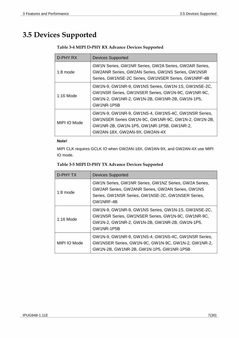
3.5 Devices Supported
Table 3-4 MIPI D-PHY RX Advance Devices Supported
D-PHY RX Devices Supported
1:8 mode
GW1N Series, GW1NR Series, GW2A Series, GW2AR Series,
GW2ANR Series, GW2AN Series, GW1NS Series, GW1NSR
Series, GW1NSE-2C Series, GW1NSER Series, GW1NRF-4B
1:16 Mode
GW1N-9, GW1NR-9, GW1NS Series, GW1N-1S, GW1NSE-2C,
GW1NSR Series, GW1NSER Series, GW1N-9C, GW1NR-9C,
GW1N-2, GW1NR-2, GW1N-2B, GW1NR-2B, GW1N-1P5,
GW1NR-1P5B
MIPI IO Mode
GW1N-9, GW1NR-9, GW1NS-4, GW1NS-4C, GW1NSR Series,
GW1NSER Series GW1N-9C, GW1NR-9C, GW1N-2, GW1N-2B,
GW1NR-2B, GW1N-1P5, GW1NR-1P5B, GW1NR-2,
GW2AN-18X, GW2AN-9X, GW2AN-4X
Note!
MIPI CLK requires GCLK IO when GW2AN-18X, GW2AN-9X, and GW2AN-4X use MIPI
IO mode.
Table 3-5 MIPI D-PHY TX Advance Devices Supported
D-PHY TX Devices Supported
1:8 mode
GW1N Series, GW1NR Series, GW1NZ Series, GW2A Series,
GW2AR Series, GW2ANR Series, GW2AN Series, GW1NS
Series, GW1NSR Series, GW1NSE-2C, GW1NSER Series,
GW1NRF-4B
1:16 Mode
GW1N-9, GW1NR-9, GW1NS Series, GW1N-1S, GW1NSE-2C,
GW1NSR Series, GW1NSER Series, GW1N-9C, GW1NR-9C,
GW1N-2, GW1NR-2, GW1N-2B, GW1NR-2B, GW1N-1P5,
GW1NR-1P5B
MIPI IO Mode
GW1N-9, GW1NR-9, GW1NS-4, GW1NS-4C, GW1NSR Series,
GW1NSER Series, GW1N-9C, GW1N-9C, GW1N-2, GW1NR-2,
GW1N-2B, GW1NR-2B, GW1N-1P5, GW1NR-1P5B
4 Functional Description 4.1 MIPI D-PHY RX Advance Structure and Function
IPUG948-1.11E 8(30)
4 Functional Description
MIPI D-PHY contains the following two D-PHY IP modules:
D-PHY RX Advance
D-PHY TX Advance
In D-PHY RX Advance and D-PHY TX Advance, HS data is converted
to serial-parallel/parallel-serial respectively. The data in LP mode can be
transmitted bi-directionally on any data lane or clock lane.
Note!
D- PHY RX Advance and D-PHY TX have different resister networks; However, both
modules support bi-directional LP communication and unidirectional HS communication.
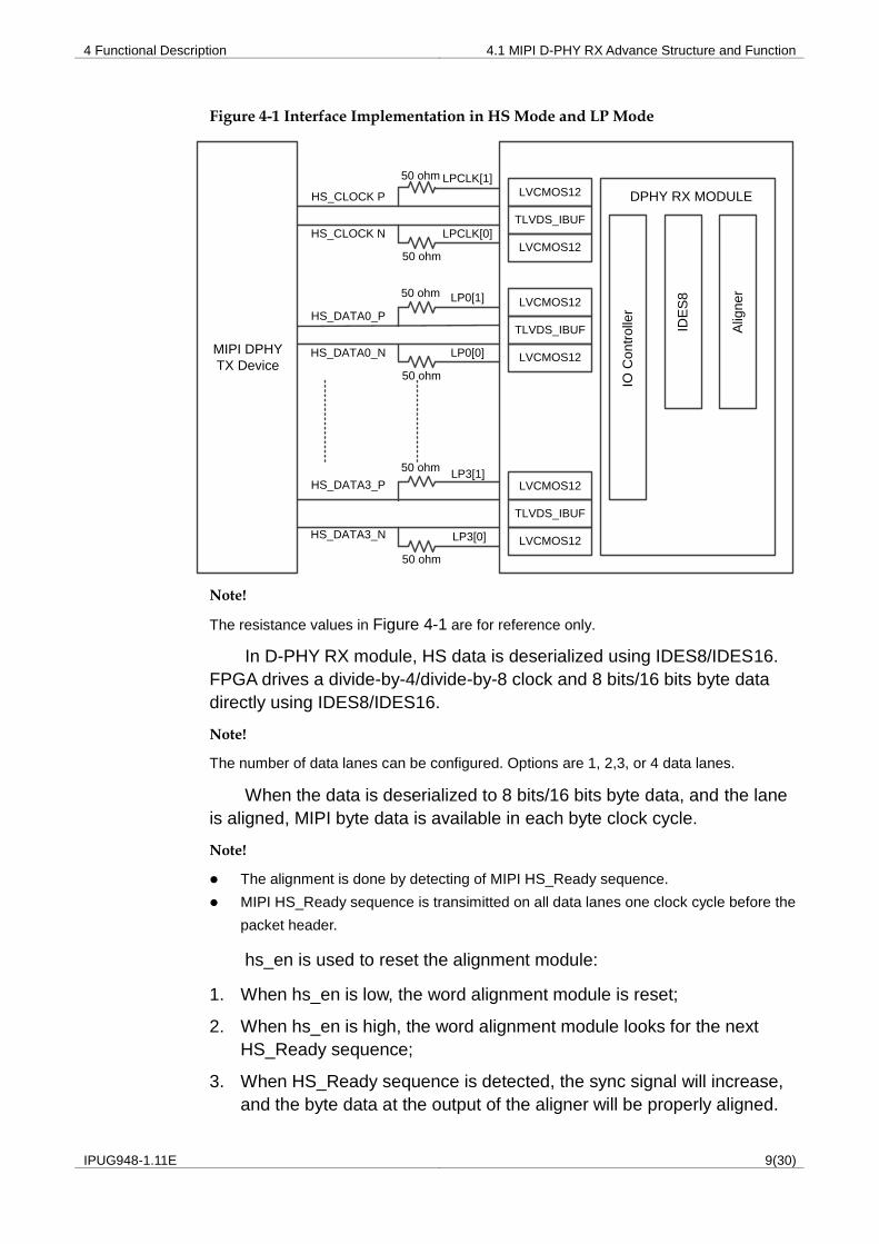
4.1 MIPI D-PHY RX Advance Structure and Function
HS data can be received on one clock lane and four clock data lanes
using D-PHY RX Advance.
Each clock and data lane uses four I/Os. Two I/O pins are used to
receive HS data with TLVDS differential I/O. TLVDS I/O is used to handle
the common 200mV mode voltage. The other two I/Os are used as serial
termination in HS mode, and can be used to transmit or receive 1.2V
CMOS data in LP mode, as shown in Figure 4-1.
4 Functional Description 4.1 MIPI D-PHY RX Advance Structure and Function
IPUG948-1.11E 9(30)
Figure 4-1 Interface Implementation in HS Mode and LP Mode
LVCMOS12
TLVDS_IBUF
LVCMOS12
50 ohm LPCLK[1]
LPCLK[0]
50 ohm
HS_CLOCK P
HS_CLOCK N
IO C
on
tro
ller
IDE
S8
Alig
ne
r
DPHY RX MODULE
MIPI DPHY
TX Device
LVCMOS12
TLVDS_IBUF
LVCMOS12
50 ohm LP0[1]
LP0[0]
50 ohm
HS_DATA0_P
HS_DATA0_N
LVCMOS12
TLVDS_IBUF
LVCMOS12
50 ohmLP3[1]
LP3[0]
50 ohm
HS_DATA3_P
HS_DATA3_N
Note!
The resistance values in Figure 4-1 are for reference only.
In D-PHY RX module, HS data is deserialized using IDES8/IDES16.
FPGA drives a divide-by-4/divide-by-8 clock and 8 bits/16 bits byte data
directly using IDES8/IDES16.
Note!
The number of data lanes can be configured. Options are 1, 2,3, or 4 data lanes.
When the data is deserialized to 8 bits/16 bits byte data, and the lane
is aligned, MIPI byte data is available in each byte clock cycle.
Note!
The alignment is done by detecting of MIPI HS_Ready sequence.
MIPI HS_Ready sequence is transimitted on all data lanes one clock cycle before the
packet header.
hs_en is used to reset the alignment module:
1. When hs_en is low, the word alignment module is reset;
2. When hs_en is high, the word alignment module looks for the next
HS_Ready sequence;
3. When HS_Ready sequence is detected, the sync signal will increase,
and the byte data at the output of the aligner will be properly aligned.
4 Functional Description 4.2 MIPI D-PHY TX Advance Structure and Function
IPUG948-1.11E 10(30)
The aligner module consists of two subsidiary modules as below:
The first module aligns the 8-bit data from the deserializer.
The second module aligns each of the data lanes to each other.
Note!
In some cases, lane alignment or lane and word alignment is not needed;
Macro compiling commands can be used to turn the word and lane alignment on and
off.
HS termination is designed to be implemented by controlling
IO_Ctrol_RX module with term_en signal. Although there is no direction
detection mechanism, the following two ways can be used to enable HS
termination:
1. The HS clock can be used to observe LP to HS data transition on one
data lane.
2. In comparison to the data lane, the clock lane will enter the HS mode in
advance and put off to the HS mode. Initialize the LP signals as input at
startup, and then observe the clock and data lanes of LP and HS.
Once the sequence is detected, term_en can be set to "low" by
enabling HS_termination.
The IO_Ctrol_RX module also controls LP signal.
Each data lane has a lp*_dir signal, which controls LP data direction
between the FPGA and the transmitting device.
You can turn on/off LP IP for each clock and data lane individually by
using Macro complier directives. This can be convenient if you require the
LP mode for one or two MIPI D-PHY data lanes.
The LP signal is defined as a 2-bit bus. Signal 1 is usually connected
to the P-side, and 0 to the N-side. This maintains the consistency with the
LP transition mode.
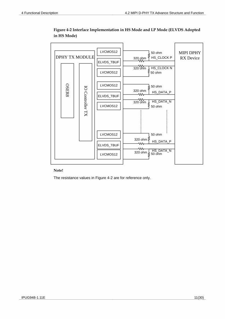
4.2 MIPI D-PHY TX Advance Structure and Function
You can use one clock lane and up to four data lanes by D-PHY TX IP.
Each lane has four I/Os. Two I/O pins transmit HS data with ELVDS type or
TLVDS type I/O. The other two I/O pins are used to provide voltage dividing
circuit in HS mode and to transmit or receive 1.2V CMOS data in LP mode.
For the circuit structure of HS data adopting ELVDS type I/O, please refer
to Figure 4-2; for the circuit structure of adopting TLVDS type I/O, please
refer to Figure 4-2.
4 Functional Description 4.2 MIPI D-PHY TX Advance Structure and Function
IPUG948-1.11E 11(30)
Figure 4-2 Interface Implementation in HS Mode and LP Mode (ELVDS Adopted
in HS Mode)
50 ohm
50 ohm
HS_CLOCK P
HS_CLOCK N
IO C
on
troller T
X
OS
ER
8
DPHY TX MODULEMIPI DPHY
RX Device
HS_DATA_P
HS_DATA_N
HS_DATA_P
HS_DATA_N
320 ohm
320 ohm
320 ohm
320 ohm
320 ohm
320 ohm
50 ohm
50 ohm
50 ohm
50 ohm
LVCMOS12
LVCMOS12
LVCMOS12
LVCMOS12
LVCMOS12
LVCMOS12
ELVDS_TBUF
ELVDS_TBUF
ELVDS_TBUF
Note!
The resistance values in Figure 4-2 are for reference only.
4 Functional Description 4.2 MIPI D-PHY TX Advance Structure and Function
IPUG948-1.11E 12(30)
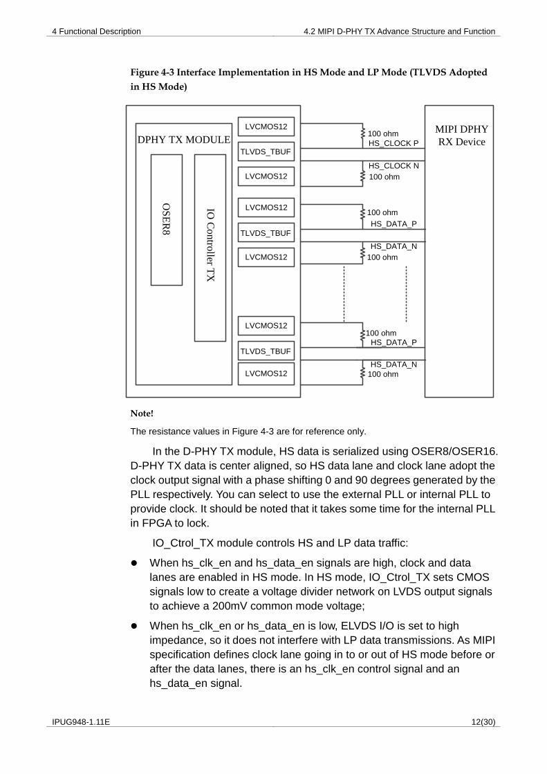
Figure 4-3 Interface Implementation in HS Mode and LP Mode (TLVDS Adopted
in HS Mode)
100 ohm
100 ohm
HS_CLOCK P
HS_CLOCK N
IO C
ontro
ller TX
OS
ER
8
DPHY TX MODULEMIPI DPHY
RX Device
HS_DATA_P
HS_DATA_N
HS_DATA_P
HS_DATA_N
100 ohm
100 ohm
100 ohm
100 ohm
LVCMOS12
LVCMOS12
LVCMOS12
LVCMOS12
LVCMOS12
LVCMOS12
TLVDS_TBUF
TLVDS_TBUF
TLVDS_TBUF
Note!
The resistance values in Figure 4-3 are for reference only.
In the D-PHY TX module, HS data is serialized using OSER8/OSER16.
D-PHY TX data is center aligned, so HS data lane and clock lane adopt the
clock output signal with a phase shifting 0 and 90 degrees generated by the
PLL respectively. You can select to use the external PLL or internal PLL to
provide clock. It should be noted that it takes some time for the internal PLL
in FPGA to lock.
IO_Ctrol_TX module controls HS and LP data traffic:
When hs_clk_en and hs_data_en signals are high, clock and data
lanes are enabled in HS mode. In HS mode, IO_Ctrol_TX sets CMOS
signals low to create a voltage divider network on LVDS output signals
to achieve a 200mV common mode voltage;
When hs_clk_en or hs_data_en is low, ELVDS I/O is set to high
impedance, so it does not interfere with LP data transmissions. As MIPI
specification defines clock lane going in to or out of HS mode before or
after the data lanes, there is an hs_clk_en control signal and an
hs_data_en signal.
4 Functional Description 4.3 MIPI IO
IPUG948-1.11E 13(30)
lp_data_dir signal controls the LP mode direction:
When hs_*_en='1', the lp*_dir control signal is overwritten;
While in LP mode, IO_Ctrol_TX module also controls the LP data
traffic.
The lp*_dir signal controls LP mode data traffic direction. The LP
signals are defined as two bit buses. Signal 1 is usually connected to the
P-side, and 0 to the N-side, which maintains consistency with LP transition
identification scheme.
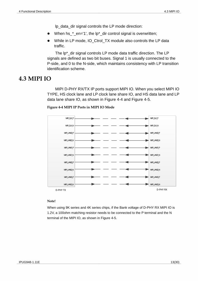
4.3 MIPI IO
MIPI D-PHY RX/TX IP ports support MIPI IO. When you select MIPI IO
TYPE, HS clock lane and LP clock lane share IO, and HS data lane and LP
data lane share IO, as shown in Figure 4-4 and Figure 4-5.
Figure 4-4 MIPI IP Ports in MIPI IO Mode
MIPI_CLK_P
MIPI_CLK_N
MIPI_LANE0_P
MIPI_LANE0_N
MIPI_LANE1_P
MIPI_LANE1_N
MIPI_LANE2_P
MIPI_LANE2_N
MIPI_LANE3_P
MIPI_LANE3_N
D-PHY TX
MIPI_CLK_P
MIPI_CLK_N
MIPI_LANE0_P
MIPI_LANE0_N
MIPI_LANE1_P
MIPI_LANE1_N
MIPI_LANE2_P
MIPI_LANE2_N
MIPI_LANE3_P
MIPI_LANE3_N
D-PHY RX
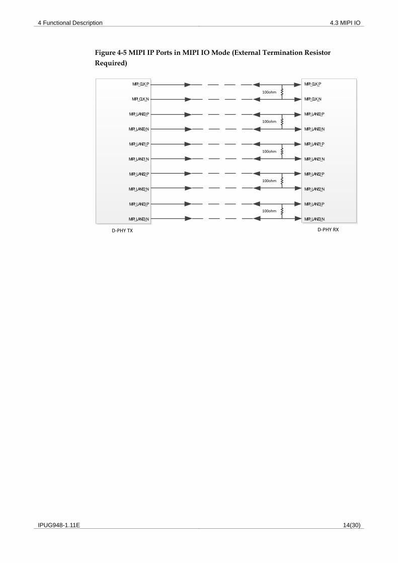
Note!
When using 9K series and 4K series chips, if the Bank voltage of D-PHY RX MIPI IO is
1.2V, a 100ohm matching resistor needs to be connected to the P terminal and the N
terminal of the MIPI IO, as shown in Figure 4-5.
4 Functional Description 4.3 MIPI IO
IPUG948-1.11E 14(30)
Figure 4-5 MIPI IP Ports in MIPI IO Mode (External Termination Resistor
Required)
MIPI_CLK_P
MIPI_CLK_N
MIPI_LANE0_P
MIPI_LANE0_N
MIPI_LANE1_P
MIPI_LANE1_N
MIPI_LANE2_P
MIPI_LANE2_N
MIPI_LANE3_P
MIPI_LANE3_N
D-PHY TX
MIPI_CLK_P
MIPI_CLK_N
MIPI_LANE0_P
MIPI_LANE0_N
MIPI_LANE1_P
MIPI_LANE1_N
MIPI_LANE2_P
MIPI_LANE2_N
MIPI_LANE3_P
MIPI_LANE3_N
D-PHY RX
100ohm
100ohm
100ohm
100ohm
100ohm
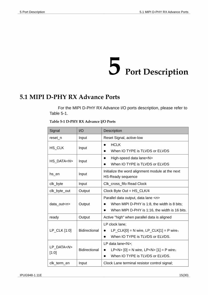
5 Port Description 5.1 MIPI D-PHY RX Advance Ports
IPUG948-1.11E 15(30)
5 Port Description
5.1 MIPI D-PHY RX Advance Ports
For the MIPI D-PHY RX Advance I/O ports description, please refer to
Table 5-1.
Table 5-1 D-PHY RX Advance I/O Ports
Signal I/O Description
reset_n Input Reset Signal, active-low
HS_CLK Input HCLK
When IO TYPE is TLVDS or ELVDS
HS_DATA<N> Input High-speed data lane<N>
When IO TYPE is TLVDS or ELVDS
hs_en Input Initialize the word alignment module at the next
HS-Ready sequence
clk_byte Input Clk_cross_fifo Read Clock
clk_byte_out Output Clock Byte Out = HS_CLK/4
data_out<n> Output
Parallel data output, data lane <n>
When MIPI D-PHY is 1:8, the width is 8 bits;
When MIPI D-PHY is 1:16, the width is 16 bits.
ready Output Active "high" when parallel data is aligned
LP_CLK [1:0] Bidirectional
LP clock lane;
LP_CLK[0] = N wire, LP_CLK[1] = P wire;
When IO TYPE is TLVDS or ELVDS.
LP_DATA<N>
[1:0] Bidirectional
LP data lane<N>;
LP<N> [0] = N wire, LP<N> [1] = P wire;
When IO TYPE is TLVDS or ELVDS.
clk_term_en Input Clock Lane terminal resistor control signal;
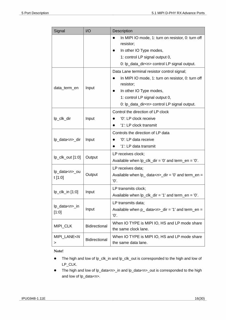
5 Port Description 5.1 MIPI D-PHY RX Advance Ports
IPUG948-1.11E 16(30)
Signal I/O Description
In MIPI IO mode, 1: turn on resistor, 0: turn off
resistor;
In other IO Type modes,
1: control LP signal output 0,
0: lp_data_dir<n> control LP signal output.
data_term_en Input
Data Lane terminal resistor control signal;
In MIPI IO mode, 1: turn on resistor, 0: turn off
resistor;
In other IO Type modes,
1: control LP signal output 0,
0: lp_data_dir<n> control LP signal output.
lp_clk_dir Input
Control the direction of LP clock
'0': LP clock receive
'1': LP clock transmit
lp_data<n>_dir Input
Controls the direction of LP data
'0': LP data receive
'1': LP data transmit
lp_clk_out [1:0] Output LP receives clock;
Available when lp_clk_dir = '0' and term_en = '0'.
lp_data<n>_ou
t [1:0] Output
LP receives data;
Available when lp_ data<n>_dir = '0' and term_en =
'0'.
lp_clk_in [1:0] Input LP transmits clock;
Available when lp_clk_dir = '1' and term_en = '0'.
lp_data<n>_in
[1:0] Input
LP transmits data;
Available when p_ data<n>_dir = '1' and term_en =
'0'.
MIPI_CLK Bidirectional When IO TYPE is MIPI IO, HS and LP mode share
the same clock lane.
MIPI_LANE<N
> Bidirectional
When IO TYPE is MIPI IO, HS and LP mode share
the same data lane.
Note!
The high and low of lp_clk_in and lp_clk_out is corresponded to the high and low of
LP_CLK. The high and low of lp_data<n>_in and lp_data<n>_out is corresponded to the high
and low of lp_data<n>.
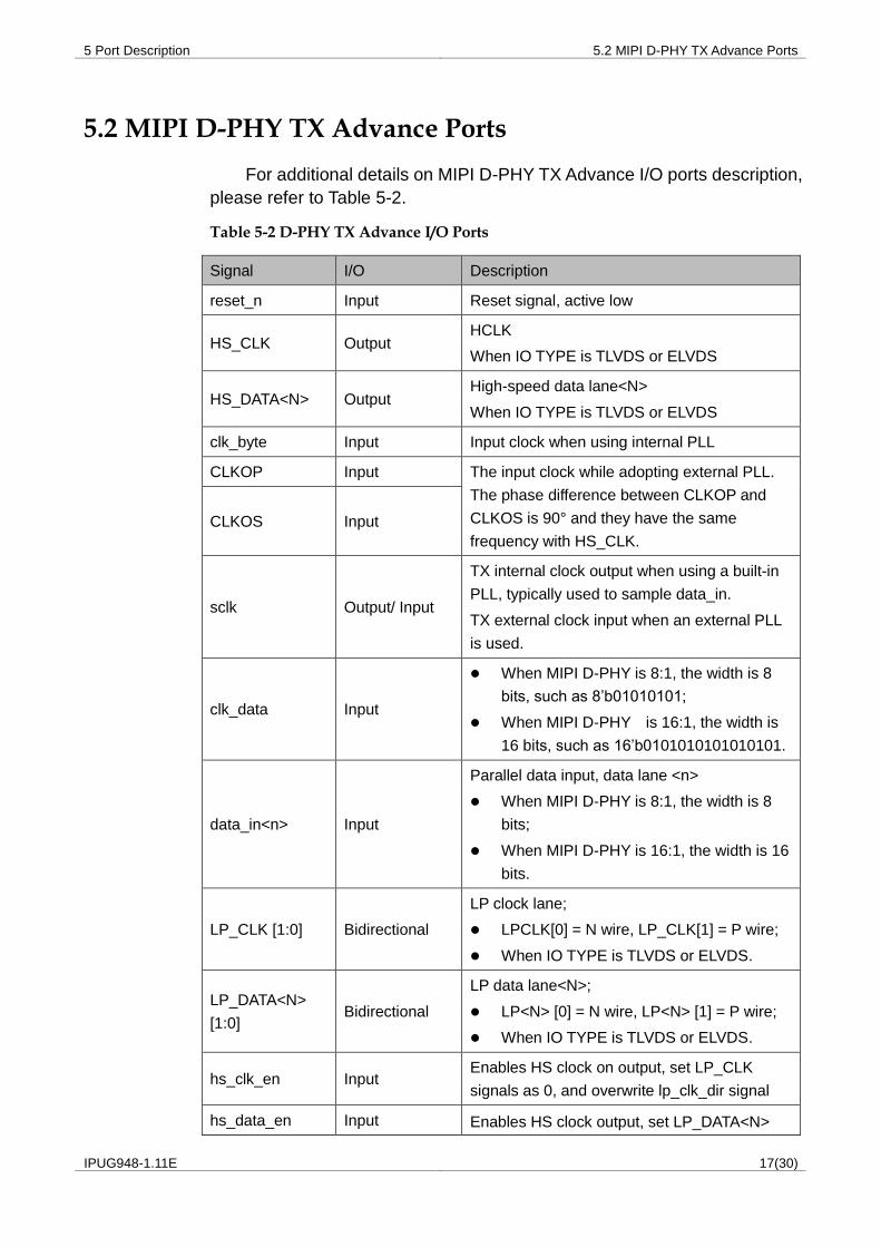
5 Port Description 5.2 MIPI D-PHY TX Advance Ports
IPUG948-1.11E 17(30)
5.2 MIPI D-PHY TX Advance Ports
For additional details on MIPI D-PHY TX Advance I/O ports description,
please refer to Table 5-2.
Table 5-2 D-PHY TX Advance I/O Ports
Signal I/O Description
reset_n Input Reset signal, active low
HS_CLK Output HCLK
When IO TYPE is TLVDS or ELVDS
HS_DATA<N> Output High-speed data lane<N>
When IO TYPE is TLVDS or ELVDS
clk_byte Input Input clock when using internal PLL
CLKOP Input The input clock while adopting external PLL.
The phase difference between CLKOP and
CLKOS is 90° and they have the same
frequency with HS_CLK.
CLKOS Input
sclk Output/ Input
TX internal clock output when using a built-in
PLL, typically used to sample data_in.
TX external clock input when an external PLL
is used.
clk_data Input
When MIPI D-PHY is 8:1, the width is 8
bits, such as 8’b01010101;
When MIPI D-PHY is 16:1, the width is
16 bits, such as 16’b0101010101010101.
data_in<n> Input
Parallel data input, data lane <n>
When MIPI D-PHY is 8:1, the width is 8
bits;
When MIPI D-PHY is 16:1, the width is 16
bits.
LP_CLK [1:0] Bidirectional
LP clock lane;
LPCLK[0] = N wire, LP_CLK[1] = P wire;
When IO TYPE is TLVDS or ELVDS.
LP_DATA<N>
[1:0] Bidirectional
LP data lane<N>;
LP<N> [0] = N wire, LP<N> [1] = P wire;
When IO TYPE is TLVDS or ELVDS.
hs_clk_en Input Enables HS clock on output, set LP_CLK
signals as 0, and overwrite lp_clk_dir signal
hs_data_en Input Enables HS clock output, set LP_DATA<N>
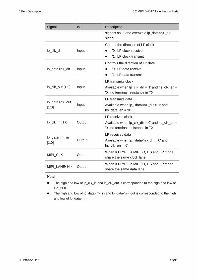
5 Port Description 5.2 MIPI D-PHY TX Advance Ports
IPUG948-1.11E 18(30)
Signal I/O Description
signals as 0, and overwrite lp_data<n>_dir
signal
lp_clk_dir Input
Control the direction of LP clock
'0': LP clock receive
'1': LP clock transmit
lp_data<n>_dir Input
Controls the direction of LP data
'0': LP data receive
'1': LP data transmit
lp_clk_out [1:0] Input
LP transmits clock
Available when lp_clk_dir = '1' and hs_clk_en =
'0', no terminal resistance in TX
lp_data<n>_out
[1:0] Input
LP transmits data
Available when lp_ data<n>_dir = '1' and
hs_data_en = '0'
lp_clk_in [1:0] Output
LP receives clock
Available when lp_clk_dir = '0' and hs_clk_en =
'0', no terminal resistance in TX
lp_data<n>_in
[1:0] Output
LP receives data
Available when lp_ data<n>_dir = '0' and
hs_clk_en = '0'
MIPI_CLK Output When IO TYPE is MIPI IO, HS and LP mode
share the same clock lane.
MIPI_LANE<N> Output When IO TYPE is MIPI IO, HS and LP mode
share the same data lane.
Note!
The high and low of lp_clk_in and lp_clk_out is corresponded to the high and low of
LP_CLK. The high and low of lp_data<n>_in and lp_data<n>_out is corresponded to the high
and low of lp_data<n>.
6 Timing Description 6.1 RX Input Signal Timing
IPUG948-1.11E 19(30)
6 Timing Description
This chapter mainly describes the input signals timing of MIPI D- PHY
RX Advance and TX Advance in HS mode.
In practical applications, RX and TX can be connected; i.e., RX output
can be TX input, and TX output can be RX input. Therefore, only the timing
for RX and TX input signals is described as below.
6.1 RX Input Signal Timing
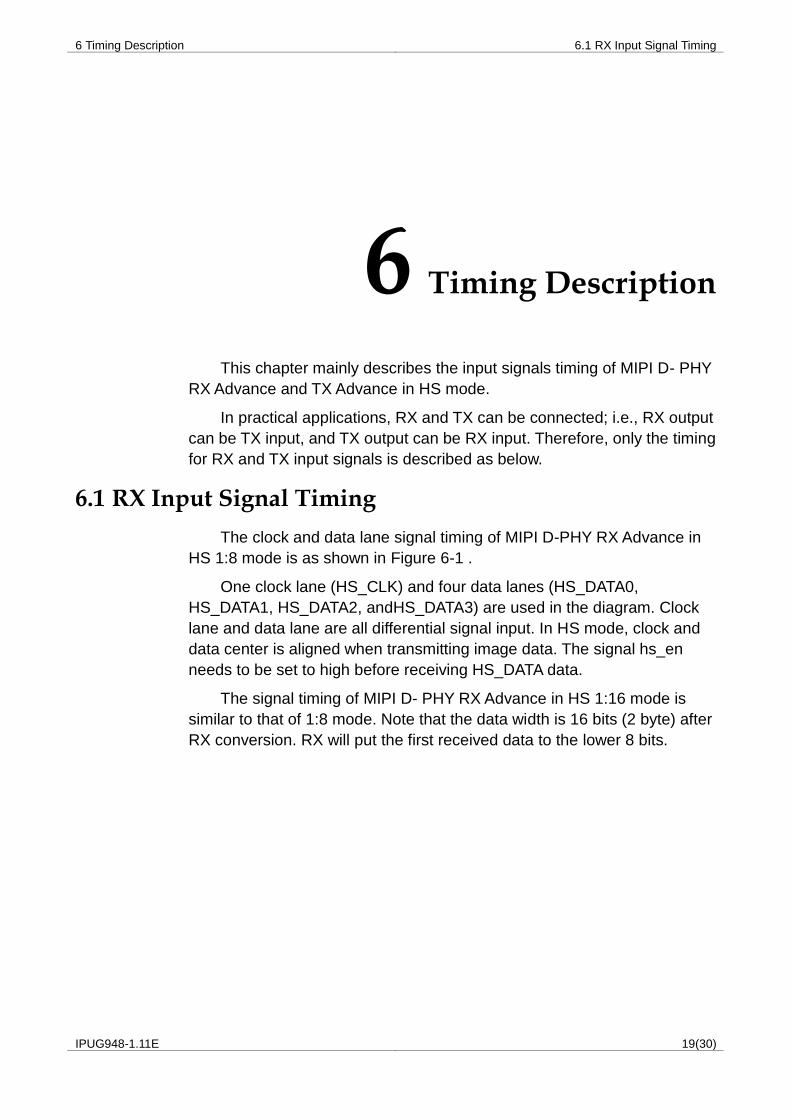
The clock and data lane signal timing of MIPI D-PHY RX Advance in
HS 1:8 mode is as shown in Figure 6-1 .
One clock lane (HS_CLK) and four data lanes (HS_DATA0,
HS_DATA1, HS_DATA2, andHS_DATA3) are used in the diagram. Clock
lane and data lane are all differential signal input. In HS mode, clock and
data center is aligned when transmitting image data. The signal hs_en
needs to be set to high before receiving HS_DATA data.
The signal timing of MIPI D- PHY RX Advance in HS 1:16 mode is
similar to that of 1:8 mode. Note that the data width is 16 bits (2 byte) after
RX conversion. RX will put the first received data to the lower 8 bits.
6 Timing Description 6.2 TX Input Signal Timing
IPUG948-1.11E 20(30)
Figure 6-1 Input Signal Timing of MIPI D-PHY RX Advance in HS 1:8 Mode
6.2 TX Input Signal Timing
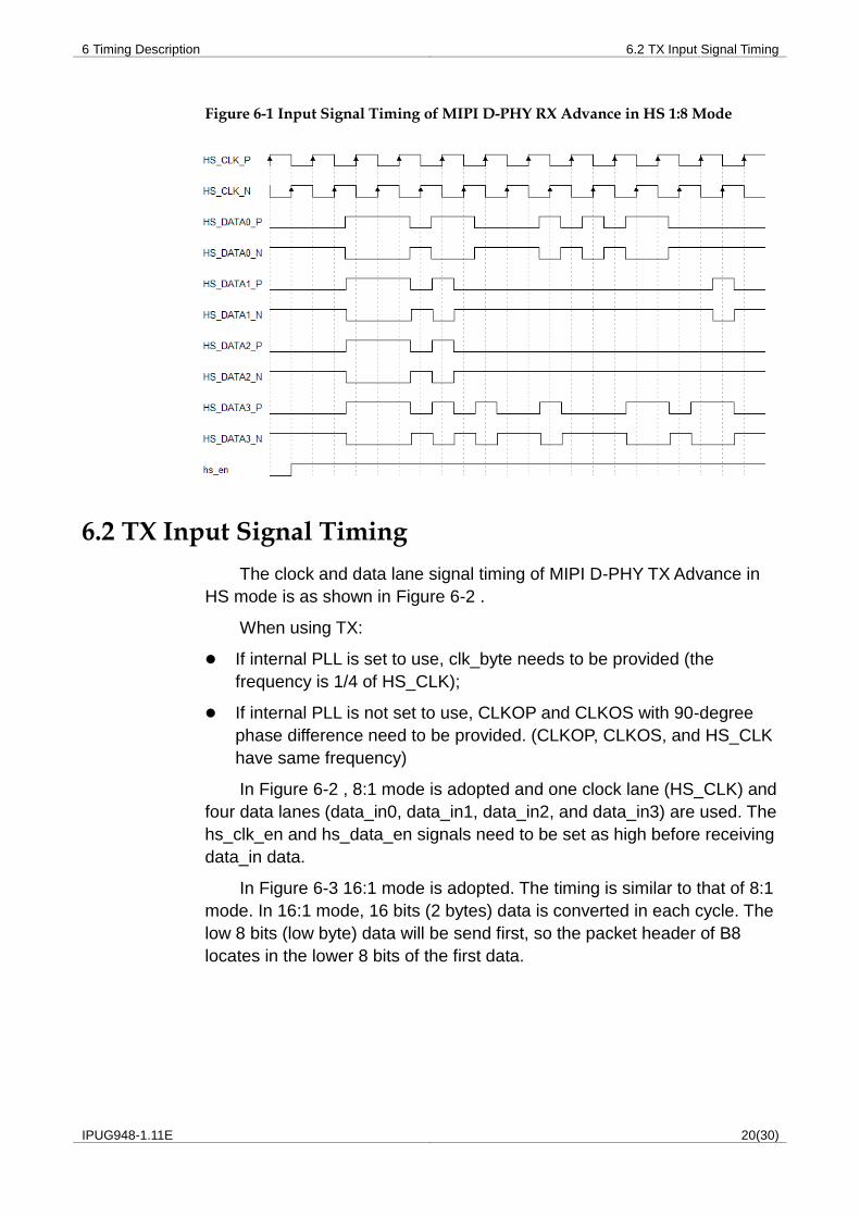
The clock and data lane signal timing of MIPI D-PHY TX Advance in
HS mode is as shown in Figure 6-2 .
When using TX:
If internal PLL is set to use, clk_byte needs to be provided (the
frequency is 1/4 of HS_CLK);
If internal PLL is not set to use, CLKOP and CLKOS with 90-degree
phase difference need to be provided. (CLKOP, CLKOS, and HS_CLK
have same frequency)
In Figure 6-2 , 8:1 mode is adopted and one clock lane (HS_CLK) and
four data lanes (data_in0, data_in1, data_in2, and data_in3) are used. The
hs_clk_en and hs_data_en signals need to be set as high before receiving
data_in data.
In Figure 6-3 16:1 mode is adopted. The timing is similar to that of 8:1
mode. In 16:1 mode, 16 bits (2 bytes) data is converted in each cycle. The
low 8 bits (low byte) data will be send first, so the packet header of B8
locates in the lower 8 bits of the first data.
6 Timing Description 6.2 TX Input Signal Timing
IPUG948-1.11E 21(30)
Figure 6-2 Input Signal Timing of MIPI D-PHY TX Advance in HS 1:8 Mode
Figure 6-3 Input Signal Timing of MIPI D-PHY TX Advance in HS 1:16 Mode
8'hB8 Byte0 Byte1
Byte1
Byte1
Byte1
Byte2
Byte2
Byte2
Byte2
8'hB8
8'hB8
8'hB88'h00
8'h00
8'h00
8'h00
Byte0
Byte0
Byte0
CLKOP
CLKOS
hs_clk_en
hs_data_en
data_in0[7:0]
data_in1[7:0]
data_in2[7:0]
data_in3[7:0]
[Byte0,8'hB8] [Byte2,Byte1] [Byte4,Byte3] [Byte6,Byte5]
16'h0000
16'h0000
16'h0000
16'h0000
[Byte0,8'hB8] [Byte2,Byte1] [Byte4,Byte3] [Byte6,Byte5]
[Byte0,8'hB8] [Byte2,Byte1] [Byte4,Byte3] [Byte6,Byte5]
[Byte0,8'hB8] [Byte2,Byte1] [Byte4,Byte3] [Byte6,Byte5]
CLKOP
CLKOS
hs_clk_en
hs_data_en
data_in0[15:0]
data_in1[15:0]
data_in2[15:0]
data_in3[15:0]
6 Timing Description 6.2 TX Input Signal Timing
IPUG948-1.11E 22(30)
7 Configuration and Generation 7.1 MIPI D-PHY RX Advance Configuration
IPUG948-1.11E 23(30)
7 Configuration and Generation
Start "IP Core Generator" from the "Tools" menu in the Gowin software
and then configure and generate the MIPI D-PHY RX and MIPI D-PHY TX
Advance.
7.1 MIPI D-PHY RX Advance Configuration
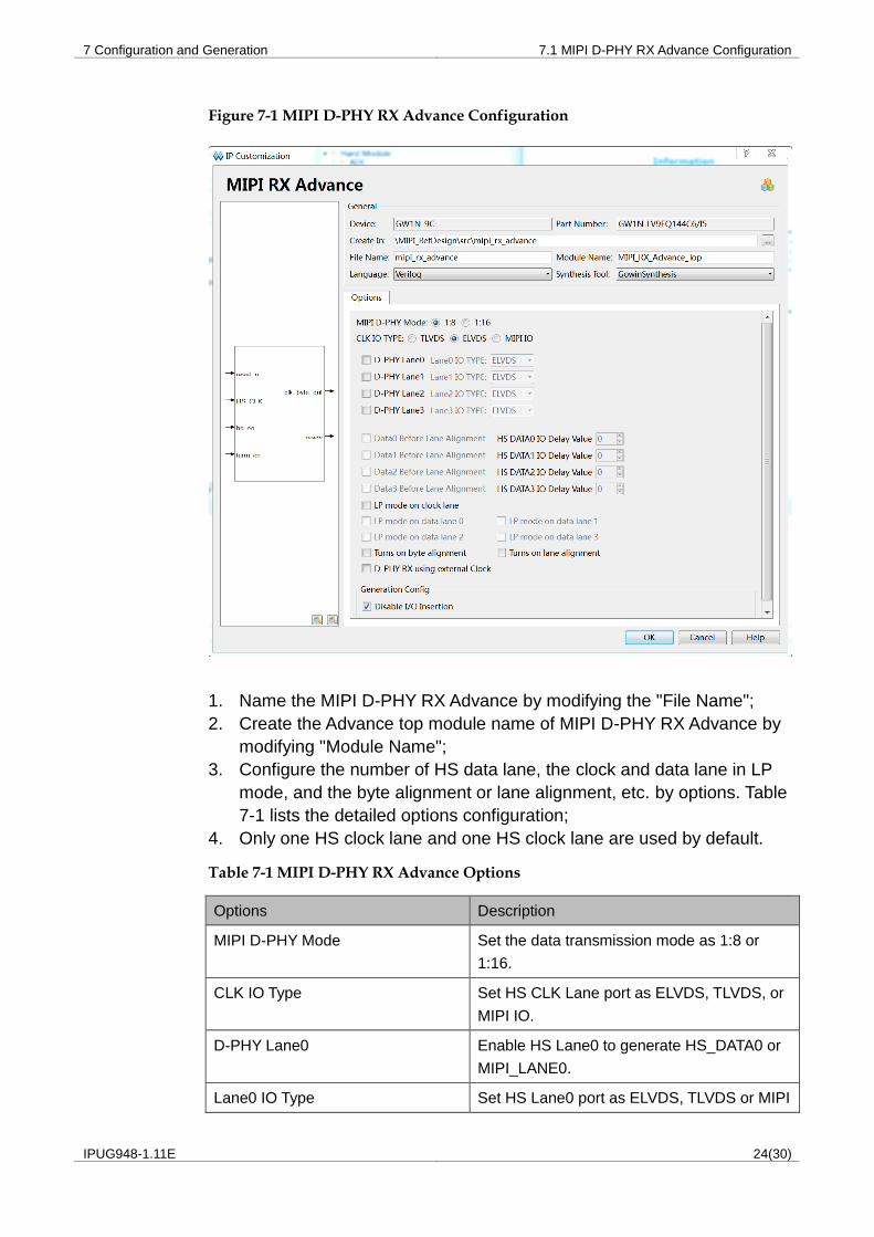
The configuration options for MIPI D-PHY RX Advance are shown in
Figure 7-1.
7 Configuration and Generation 7.1 MIPI D-PHY RX Advance Configuration
IPUG948-1.11E 24(30)
Figure 7-1 MIPI D-PHY RX Advance Configuration
1. Name the MIPI D-PHY RX Advance by modifying the "File Name";
2. Create the Advance top module name of MIPI D-PHY RX Advance by
modifying "Module Name";
3. Configure the number of HS data lane, the clock and data lane in LP
mode, and the byte alignment or lane alignment, etc. by options. Table
7-1 lists the detailed options configuration;
4. Only one HS clock lane and one HS clock lane are used by default.
Table 7-1 MIPI D-PHY RX Advance Options
Options Description
MIPI D-PHY Mode Set the data transmission mode as 1:8 or
1:16.
CLK IO Type Set HS CLK Lane port as ELVDS, TLVDS, or
MIPI IO.
D-PHY Lane0 Enable HS Lane0 to generate HS_DATA0 or
MIPI_LANE0.
Lane0 IO Type Set HS Lane0 port as ELVDS, TLVDS or MIPI
7 Configuration and Generation 7.1 MIPI D-PHY RX Advance Configuration
IPUG948-1.11E 25(30)
Options Description
IO.
D-PHY Lane1 Enable HS Lane3 to generate HS_DATA0 or
MIPI_LANE0.
Lane1 IO Type Set HS Lane1 port as ELVDS、TLVDS or
MIPI IO.
D-PHY Lane2 Enable HS Lane3 to generate HS_DATA0 or
MIPI_LANE0.
Lane2 IO Type Set HS Lane2 port as ELVDS、TLVDS or
MIPI IO.
D-PHY Lane3 Enable HS Lane3 to generate HS_DATA0 or
MIPI_LANE0.
Lane3 IO Type Set HS Lane3 port as ELVDS, TLVDS or MIPI
IO.
Data3/2/1/0 Before Lane Alignment Set whether to generate data port, output data
before entering the lane alignment module;
HS Lanes can be set independently.
HS Data3/2/1/0 IO Delay Value Set the IO Delay value of HS Lane ports
HS Lanes can be set independently.
LP mode on clock lane Generate LP_CLK[1:0] and the other I/O ports
for LP mode on clock lane.
LP mode on data lane0 Generate LP_DATA0[1:0] and the other I/O
ports for LP mode on data lane0.
LP mode on data lane1 Generate LP_DATA1[1:0] and the other I/O
ports for LP mode on data lane1.
LP mode on data lane2 Generate LP_DATA2[1:0] and the other I/O
ports for LP mode on data lane2.
LP mode on data lane3 Generate LP_DATA3[1:0] and the other I/O
ports for LP mode on data lane3.
Turns on byte alignment Check this option to enable byte alignment,
which is used to align the bytes after
deserializing on one lane.
Turns on lane alignment Check this option to enable lane alignment,
which is used to align different data lanes.
D-PHY RX using external Clock Check this option for RX module to use an
external clock (clk_byte), and data_out0/1/2/3
will align at clk_byte.
7 Configuration and Generation 7.2 MIPI D-PHY TX Advance Configuration
IPUG948-1.11E 26(30)
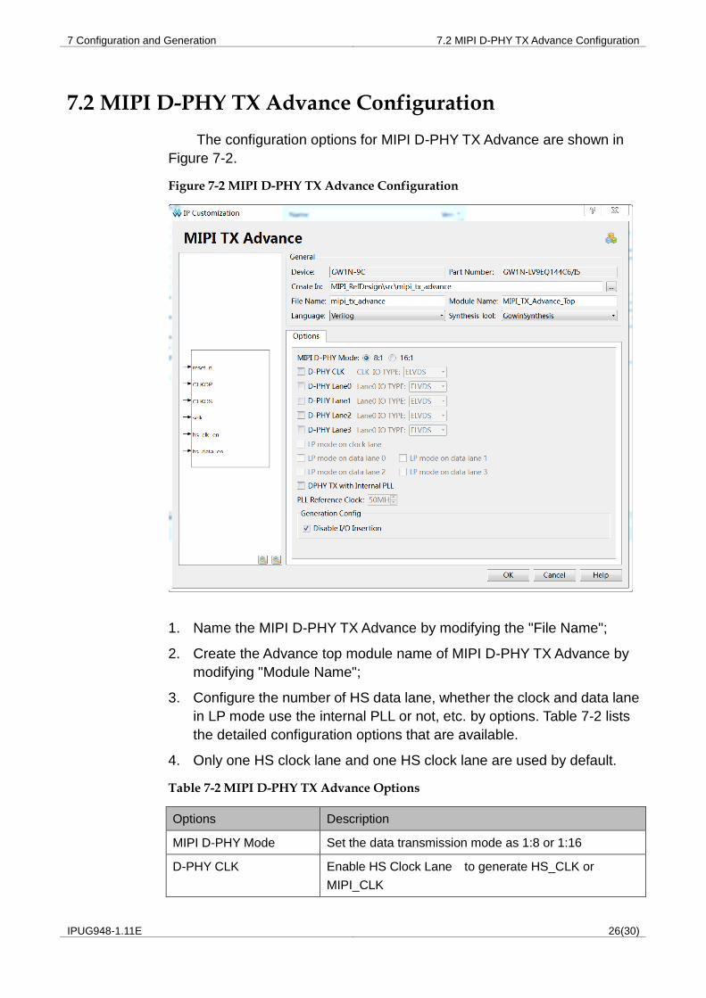
7.2 MIPI D-PHY TX Advance Configuration
The configuration options for MIPI D-PHY TX Advance are shown in
Figure 7-2.
Figure 7-2 MIPI D-PHY TX Advance Configuration
1. Name the MIPI D-PHY TX Advance by modifying the "File Name";
2. Create the Advance top module name of MIPI D-PHY TX Advance by
modifying "Module Name";
3. Configure the number of HS data lane, whether the clock and data lane
in LP mode use the internal PLL or not, etc. by options. Table 7-2 lists
the detailed configuration options that are available.
4. Only one HS clock lane and one HS clock lane are used by default.
Table 7-2 MIPI D-PHY TX Advance Options
Options Description
MIPI D-PHY Mode Set the data transmission mode as 1:8 or 1:16
D-PHY CLK Enable HS Clock Lane to generate HS_CLK or
MIPI_CLK
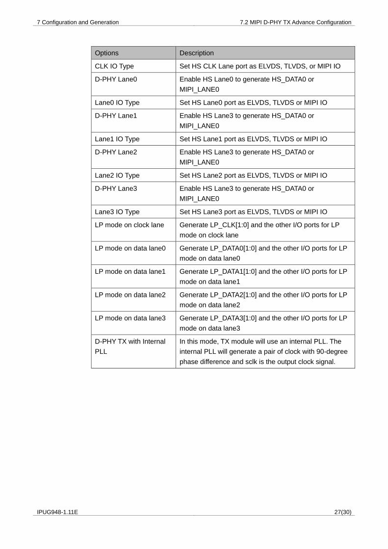
7 Configuration and Generation 7.2 MIPI D-PHY TX Advance Configuration
IPUG948-1.11E 27(30)
Options Description
CLK IO Type Set HS CLK Lane port as ELVDS, TLVDS, or MIPI IO
D-PHY Lane0 Enable HS Lane0 to generate HS_DATA0 or
MIPI_LANE0
Lane0 IO Type Set HS Lane0 port as ELVDS, TLVDS or MIPI IO
D-PHY Lane1 Enable HS Lane3 to generate HS_DATA0 or
MIPI_LANE0
Lane1 IO Type Set HS Lane1 port as ELVDS, TLVDS or MIPI IO
D-PHY Lane2 Enable HS Lane3 to generate HS_DATA0 or
MIPI_LANE0
Lane2 IO Type Set HS Lane2 port as ELVDS, TLVDS or MIPI IO
D-PHY Lane3 Enable HS Lane3 to generate HS_DATA0 or
MIPI_LANE0
Lane3 IO Type Set HS Lane3 port as ELVDS, TLVDS or MIPI IO
LP mode on clock lane Generate LP_CLK[1:0] and the other I/O ports for LP
mode on clock lane
LP mode on data lane0 Generate LP_DATA0[1:0] and the other I/O ports for LP
mode on data lane0
LP mode on data lane1 Generate LP_DATA1[1:0] and the other I/O ports for LP
mode on data lane1
LP mode on data lane2 Generate LP_DATA2[1:0] and the other I/O ports for LP
mode on data lane2
LP mode on data lane3 Generate LP_DATA3[1:0] and the other I/O ports for LP
mode on data lane3
D-PHY TX with Internal
PLL
In this mode, TX module will use an internal PLL. The
internal PLL will generate a pair of clock with 90-degree
phase difference and sclk is the output clock signal.
Appendix A MIPI D-PHY Data Rates
IPUG948-1.11E 28(30)
Appendix A MIPI D-PHY Data Rates
Appendix A MIPI D-PHY Data Rates
IPUG948-1.11E 29(30)
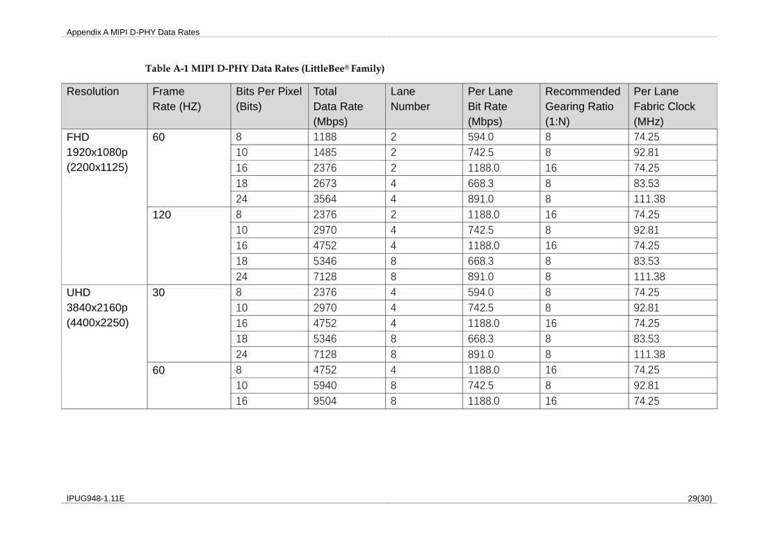
Table A-1 MIPI D-PHY Data Rates (LittleBee® Family)
Resolution Frame
Rate (HZ)
Bits Per Pixel
(Bits)
Total
Data Rate
(Mbps)
Lane
Number
Per Lane
Bit Rate
(Mbps)
Recommended
Gearing Ratio
(1:N)
Per Lane
Fabric Clock
(MHz)
FHD
1920x1080p
(2200x1125)
60 8 1188 2 594.0 8 74.25
10 1485 2 742.5 8 92.81
16 2376 2 1188.0 16 74.25
18 2673 4 668.3 8 83.53
24 3564 4 891.0 8 111.38
120 8 2376 2 1188.0 16 74.25
10 2970 4 742.5 8 92.81
16 4752 4 1188.0 16 74.25
18 5346 8 668.3 8 83.53
24 7128 8 891.0 8 111.38
UHD
3840x2160p
(4400x2250)
30 8 2376 4 594.0 8 74.25
10 2970 4 742.5 8 92.81
16 4752 4 1188.0 16 74.25
18 5346 8 668.3 8 83.53
24 7128 8 891.0 8 111.38
60 8 4752 4 1188.0 16 74.25
10 5940 8 742.5 8 92.81
16 9504 8 1188.0 16 74.25
Appendix A MIPI D-PHY Data Rates
IPUG948-1.11E 30(30)
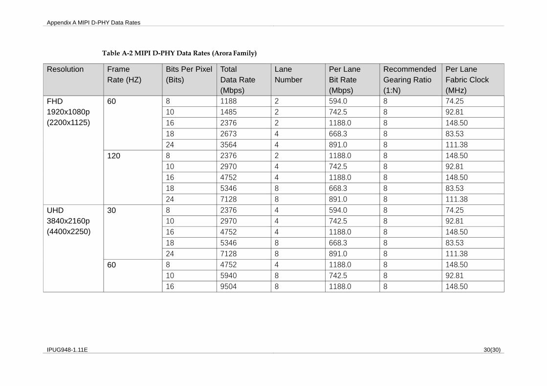
Table A-2 MIPI D-PHY Data Rates (Arora Family)
Resolution Frame
Rate (HZ)
Bits Per Pixel
(Bits)
Total
Data Rate
(Mbps)
Lane
Number
Per Lane
Bit Rate
(Mbps)
Recommended
Gearing Ratio
(1:N)
Per Lane
Fabric Clock
(MHz)
FHD
1920x1080p
(2200x1125)
60 8 1188 2 594.0 8 74.25
10 1485 2 742.5 8 92.81
16 2376 2 1188.0 8 148.50
18 2673 4 668.3 8 83.53
24 3564 4 891.0 8 111.38
120 8 2376 2 1188.0 8 148.50
10 2970 4 742.5 8 92.81
16 4752 4 1188.0 8 148.50
18 5346 8 668.3 8 83.53
24 7128 8 891.0 8 111.38
UHD
3840x2160p
(4400x2250)
30 8 2376 4 594.0 8 74.25
10 2970 4 742.5 8 92.81
16 4752 4 1188.0 8 148.50
18 5346 8 668.3 8 83.53
24 7128 8 891.0 8 111.38
60 8 4752 4 1188.0 8 148.50
10 5940 8 742.5 8 92.81
16 9504 8 1188.0 8 148.50

Related Documents


