1 Government Polytechnic, Muzaffarpur ELECTRONIC CONSTRUCTION AND REPAIR LAB Subject Code: 1620407 Experiment:1& 3 Aim of experiment:Construction of a Battery Eliminator Apparatus required AC Plug 15-18V Transformer Full Wave Bridge Rectifier LM317 Voltage Regulator Heat Sink 2200μF electrolytic capacitor 100μF electrolytic capacitor Rotary Switch 240Ω Resistor 48Ω Resistor 336Ω Resistor 624Ω Resistor 912Ω Resistor 1488Ω Resistor (1.5KΩ is fine) 2064Ω Resistor (2KΩ is fine)

Welcome message from author
This document is posted to help you gain knowledge. Please leave a comment to let me know what you think about it! Share it to your friends and learn new things together.
Transcript

1
Government Polytechnic, Muzaffarpur
ELECTRONIC CONSTRUCTION AND REPAIR LAB
Subject Code: 1620407
Experiment:1& 3
Aim of experiment:Construction of a Battery Eliminator
Apparatus required
AC Plug
15-18V Transformer
Full Wave Bridge Rectifier
LM317 Voltage Regulator
Heat Sink
2200μF electrolytic capacitor
100μF electrolytic capacitor
Rotary Switch
240Ω Resistor
48Ω Resistor
336Ω Resistor
624Ω Resistor
912Ω Resistor
1488Ω Resistor (1.5KΩ is fine)
2064Ω Resistor (2KΩ is fine)
2
Theory of experiment
A battery eliminator is any device which supplies the necessary DC power to a device,
replacing the need for batteries.
For example, say if we have a device that is normally powered by batteries, such as a
calculator. It may receive 4 'AA' or 'AAA' batteries, depending on the calculator. In this
case, the DC voltage that the calculator needs is 6 volts, since 4 'AA' batteries in series adds
up to 6VDC. We can power the calculator without batteries if we supply it with the 6VDC.
So any device which allows us to bypass the use of batteries and power the device still is a
battery eliminator.
Now , we will build a simple, effective battery eliminator which supplies many of the typical
voltages that batteries would, only without the need for batteries.
Battery Eliminator Schematic Diagram
3
a battery eliminator, it creates DC voltage from the AC mains voltage from a wall outlet. To
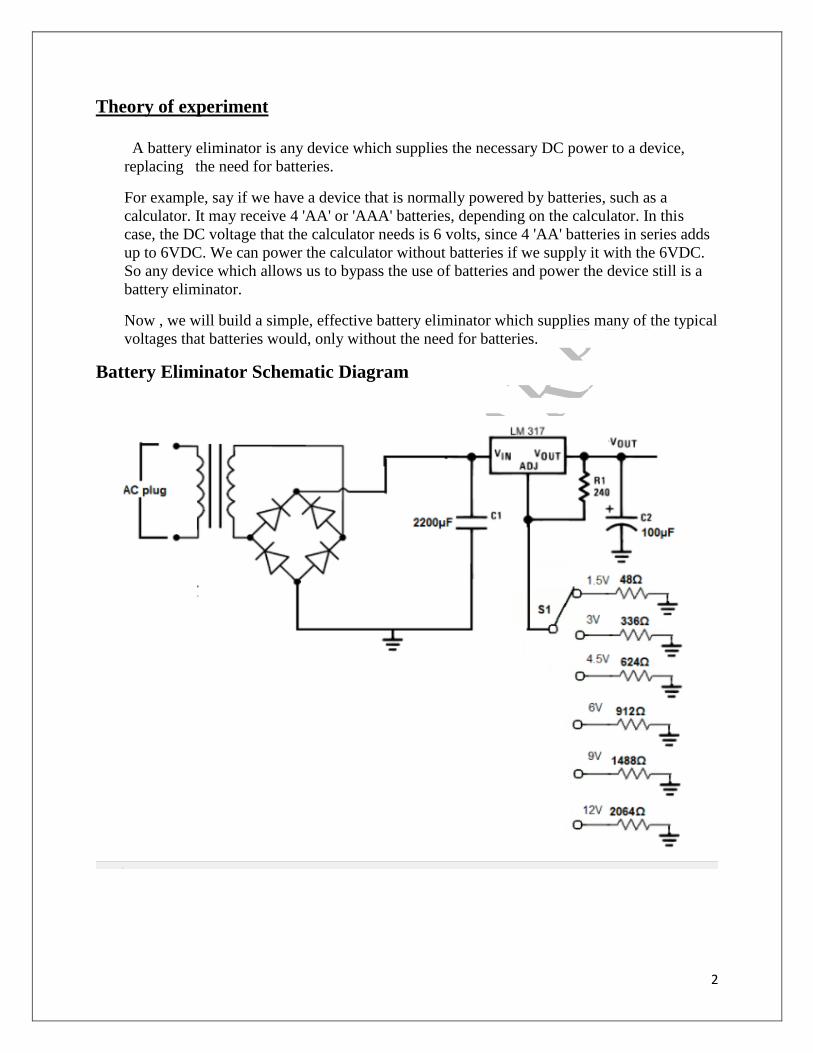
build a battery eliminator, purchase a 3-prong AC plug. It can also work with a two-prong AC
plug. But having a 3-prong plug is better because ground provides
better against possible electric fires.
Transformer- After the AC plug, we need a step-down
transformer. The tranformer's job is to take the 120V AC We'll
now go over each part of this circuit and go over the role each
component plays, so that you can know how this circuit works in
its entirety.
AC Plug- The first part of the circuit is the AC plug. When we create voltage from the mains
line and step it down to 15-18 volts. This is because our battery eliminator will supply variable
DC voltage of 1-20V. Therefore, we lower the very high voltage that we get from the mains
outlet from the wall into a smaller voltage. It must still exceed the voltage of the DC which we
want to output. Since we want to create up to 20VDC variable voltage output, we need a
transformer that converts the mains voltage to a voltage that is higher than this 20V. A step-
down transformer is a great device for lowering voltage from a mains AC voltage line.
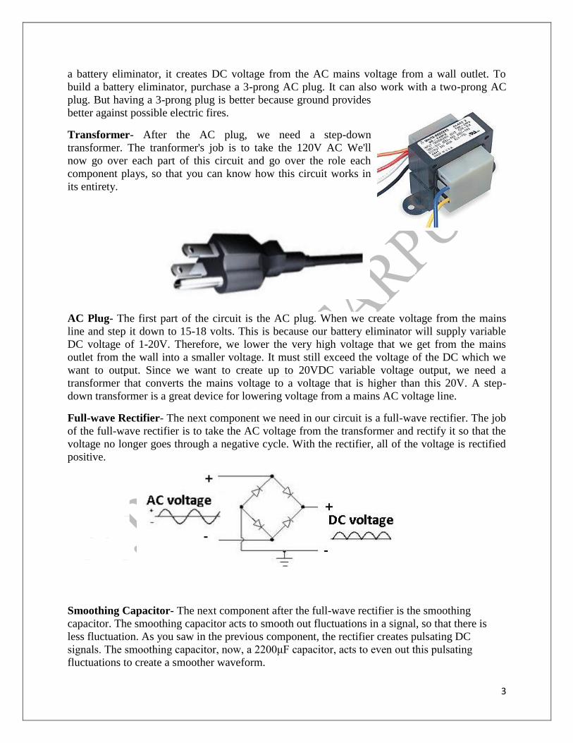
Full-wave Rectifier- The next component we need in our circuit is a full-wave rectifier. The job
of the full-wave rectifier is to take the AC voltage from the transformer and rectify it so that the
voltage no longer goes through a negative cycle. With the rectifier, all of the voltage is rectified
positive.
Smoothing Capacitor- The next component after the full-wave rectifier is the smoothing
capacitor. The smoothing capacitor acts to smooth out fluctuations in a signal, so that there is
less fluctuation. As you saw in the previous component, the rectifier creates pulsating DC
signals. The smoothing capacitor, now, a 2200μF capacitor, acts to even out this pulsating
fluctuations to create a smoother waveform.
4
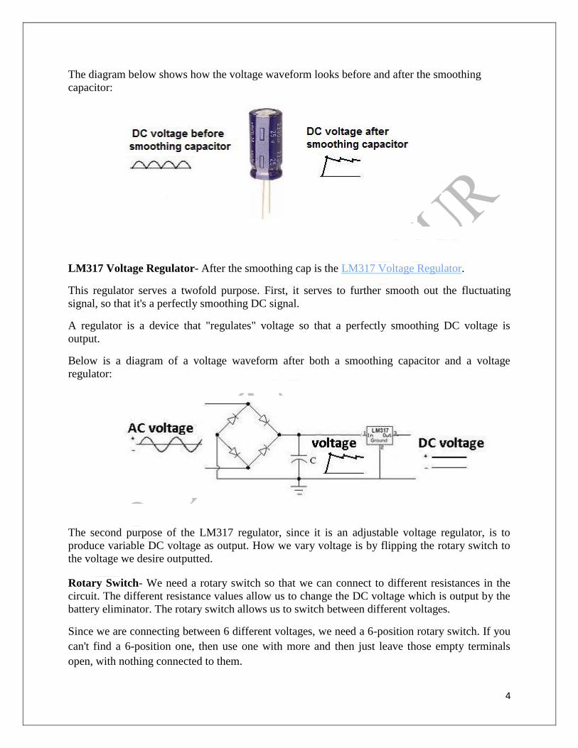
The diagram below shows how the voltage waveform looks before and after the smoothing
capacitor:
LM317 Voltage Regulator- After the smoothing cap is the LM317 Voltage Regulator.
This regulator serves a twofold purpose. First, it serves to further smooth out the fluctuating
signal, so that it's a perfectly smoothing DC signal.
A regulator is a device that "regulates" voltage so that a perfectly smoothing DC voltage is
output.
Below is a diagram of a voltage waveform after both a smoothing capacitor and a voltage
regulator:
The second purpose of the LM317 regulator, since it is an adjustable voltage regulator, is to
produce variable DC voltage as output. How we vary voltage is by flipping the rotary switch to
the voltage we desire outputted.
Rotary Switch- We need a rotary switch so that we can connect to different resistances in the
circuit. The different resistance values allow us to change the DC voltage which is output by the
battery eliminator. The rotary switch allows us to switch between different voltages.
Since we are connecting between 6 different voltages, we need a 6-position rotary switch. If you
can't find a 6-position one, then use one with more and then just leave those empty terminals
open, with nothing connected to them.

5
Resistors Connected to Rotary Switch- We attach resistors to the rotary switch, S1, to create
different voltage outputs at each of the terminals of the switch. We use 48Ω, 336Ω, 624Ω, 912Ω,
1488Ω, and 2064Ω resistors. The reason we use these resistors is because the output voltage
created by the LM317 voltage regulator is produced according to the formula, VOUT= 1.25V (1
+ R2/R1). The recommended resistor value to use for R1 by the manufacturer is 240Ω. So this
resistor value is fixed. To create different output voltages, we vary the value of resistor R2. By
making R2 48Ω, we create 1.5V as output. By making the value 336Ω, we create 3V as output.
By making the value 624Ω, we create 4.5V as output. By making the value 912Ω, we create 6V
as output. By making the value 1488Ω, we create 9V as output. By making the value 2064Ω, we
create 12V as output.
We realize that getting resistors of value 1488Ω and 2064Ω is difficult, so you can get use
1.5KΩ and 2KΩ as replacements to simplify the value.
Again, these resistance values are what create the various output voltages.
Heat sink- One thing we must do to the voltage regulator is attach a heat sink to it. This is vital
for this application.
This is because when we use a regulator, we input a voltage into it and it outputs the voltage,
based on the values of resistor R1 and the resistance value which the rotary switch is connected
to. When the rotary switch is connected to its highest resistance, it doesn't dissipate that much
heat. Since our transformer outputs 15-18V, when the rotary is set to 2.6KΩ, the regulator
outputs 12V. 15-12V=3V. Thus, not that much wasted voltage is created. However, if the
potentiometer is set to 48Ω, the regulator outputs approximately 1.5. 15V-1.5V= 13.5V of
wasted, dissipated energy. This creates a lot of heat, since the voltage difference between input
and output voltage is so great. Any difference appears as heat. So the greater the difference, the
greater the heat. This is the r reason it is vital to attach a heat sink to the regulator. When the
difference between input and output voltage is great, it appears as heat. We must have a way to
dissipate this heat, or else it can damage or destroy the circuitry of the battery eliminator. The
way to do this is to use a heat sink.

6
C2 Capacitor- The C2 capacitor acts again as a load balancer. It helps to smooth out any
fluctuations that may exist on the output of the regulator.
And this is how a simple battery eliminator can be built that allows for voltage adjustment.
Conclusion:
7
Government Polytechnic, Muzaffarpur
ELECTRONIC CONSTRUCTION AND REPAIR LAB
Subject Code: 1620407
Experiment:1 & 3
Aim of experiment: Construction Assembling of a Stabilizer
Apparatus required
Resistor R1 & R2 = 10KΩ
Resistor R3 = 470KΩ
Variable Resistor = 10KΩ
Capacitor C1 = 1000 µF/25 V
Diode D1 & D2 = 1N 4007
Zener Diode Z1 & Z2 = 4.7 V/ 400mW
Transformer TR1 = 0V - 12 V , 500mA
Transformer TR2 = 9V-0V-9V, 5A.
Op-Amp = LM 741
Transistor = BC 547
Relay = DPDT, 12V, 200Ω.
LED = Red (1)
Voltmeter = 1 Pcs.
Theory of experiment
8
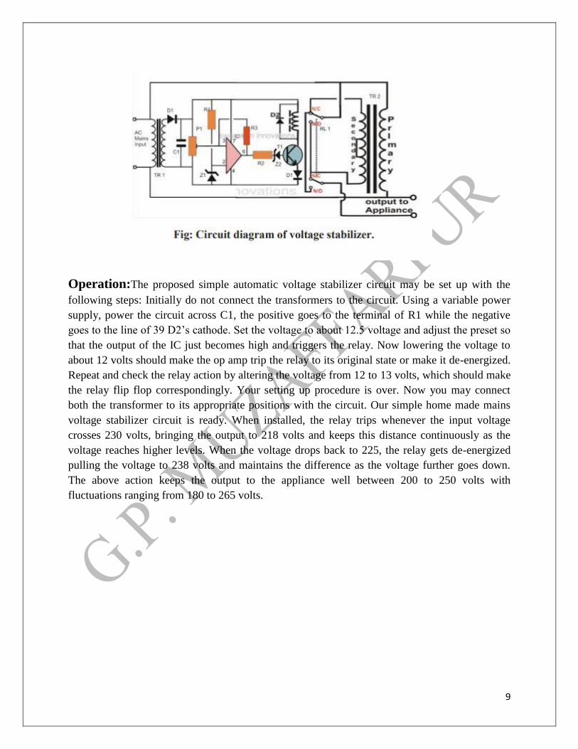
A voltage stabilizer is a device which is used to sense inappropriate voltage levels and correct
them to produce a reasonably stable output at the output where the load is connected. Here we
will study the design of a simple automatic mains AC voltage stabilizer which can be applied for
the above purpose. Referring to the figure we find that the whole circuit is configured with the
single op amp IC 741. It becomes the control section of the whole design. The IC is wired as a
comparator, we all know how well this mode suits the IC 741 and other op amps. It's two inputs
are suitable rigged for the said operations. Pin #2 of the IC is clamped to a reference level,
created by the resistor R1 and the zener diode, while pin #3 is applied with the sample voltage
from the transformer or the supply source. This voltage becomes the sensing voltage for the IC
and is directly proportional to the varying AC input of our mains supply. The preset is used to set
the triggering point or the threshold point at which the voltage may be assumed to be dangerous
or inappropriate. We will discuss this in the setting up procedure section. The pin #6 which is the
output of the IC, goes high as soon as pin #3 reaches the set point and activates the
transistor/relay stage. In case the mains voltage crosses a predetermined threshold, the ICs non
inverting detects it and its output immediately goes high, switching ON the transistor and the
relay for the desired actions. The relay, which is a DPDT type of relay, has its contacts wired up
to a transformer, which is an ordinary transformer modified to perform the function of a
stabilizer transformer. It’s primary and secondary windings are interconnected in such a manner
that through appropriate switching of its taps, the transformer is able to add or deduct a certain
magnitude of AC mains voltage and produce the resultant to the output connected load.
The relay contacts are appropriately integrated to the transformer taps for executing the
above actions as per the commands given by the op amp output. So if the input AC voltage tends
to increase a set threshold value, the transformer deducts some voltage and tries to stop the
voltage from reaching dangerous levels and vice versa during low voltage situations.
Circuit Diagram:
9
Operation:The proposed simple automatic voltage stabilizer circuit may be set up with the
following steps: Initially do not connect the transformers to the circuit. Using a variable power
supply, power the circuit across C1, the positive goes to the terminal of R1 while the negative
goes to the line of 39 D2’s cathode. Set the voltage to about 12.5 voltage and adjust the preset so
that the output of the IC just becomes high and triggers the relay. Now lowering the voltage to
about 12 volts should make the op amp trip the relay to its original state or make it de-energized.
Repeat and check the relay action by altering the voltage from 12 to 13 volts, which should make
the relay flip flop correspondingly. Your setting up procedure is over. Now you may connect
both the transformer to its appropriate positions with the circuit. Our simple home made mains
voltage stabilizer circuit is ready. When installed, the relay trips whenever the input voltage
crosses 230 volts, bringing the output to 218 volts and keeps this distance continuously as the
voltage reaches higher levels. When the voltage drops back to 225, the relay gets de-energized
pulling the voltage to 238 volts and maintains the difference as the voltage further goes down.
The above action keeps the output to the appliance well between 200 to 250 volts with
fluctuations ranging from 180 to 265 volts.

10
Limitation:
When installed, the relay trips whenever the input voltage crosses 230 volts, bringing the
output to 218 volts and keeps this distance continuously as the voltage reaches higher
levels.
When the voltage drops back to 225, the relay gets de-energized pulling the voltage to
238 volts and maintains the difference as the voltage further goes down.
The above action keeps the output to the appliance well between 200 to 250 volts with
fluctuations ranging from 180 to 265 volts.

11
Government Polytechnic, Muzaffarpur
ELECTRONIC CONSTRUCTION AND REPAIR LAB
Subject Code: 1620407
Experiment:2
Aim of experiment: Soldering Practice: Connecting circuit components
Apparatus required
The basic tools that are used for this purpose are
Soldering Iron
Solder Wire [Alloy]
Flux
PCB and the components that are to be soldered
The soldering iron is the heat source tool for the process. It should be of high quality. Of course
the price may increase with the quality, but the soldering will be perfect. Usually a 25 Watt
soldering iron is adequate for the process. A higher watt device may bring too much heat to the
PCB and will surely damage the sensitive components. A lesser watt device may not have
adequate heat and thus is prone to be extensively used. This may also cause extensive heat
damage.
The solder wire is used to fix the components like resistors, capacitors and so on to the PCB in
the given fields. The leads of the devices are connected to the track of the PCB by melting the
soldering wire to the junction. When the heat from the soldering iron touches the soldering wire
it starts melting and this melted wire when introduced to the junction, joins the components to
the track firmly.
The soldering wire is actually an alloy of tin and lead in the ratio 60:40. This is the best ratio that
is considered for soldering in PCB’s. There are other proportions of this alloy and they are
considered low quality as the tin content with respect to lead will be lower.
A high quality solder wire will have a melting point of about 250 degree Celsius and will have a
very high conductivity along with a shiny appearance. When a high quality solder wire is used
to connect the components to the PCB, there is to be no fear of corrosion in future.
Flux is another important component that is used in soldering purposes. It is sealed to the core of
the solder wire before soldering. The flux is used to reduce the surface tension of the solder wire
in its melting point. Thus, it acts as a wetting agent and wets the parts that are to be joined to the
PCB. This also helps in the proper heat transfer from the solder iron to the solder wire.

12
Another main use of the flux is to prevent oxidation of both the solder wire and the components
that are added to the PCB. The Tin-Lead alloy that is used as solder wire may have no problem
when attached to copper. But they do not attach so well, when in contact with the oxides of
copper. The oxides of copper mostly form when the temperature is increased for soldering. The
flux can prevent the formation of metal oxide as they are nearly inert at room temperature and
become strongly reduced when the temperature increases. The use of flux causes the rise of
smoke when the soldering process continues. During this time the flux acts as a catalyst and
helps in removing the oxidants and thus cause a better solder joint.
Soldering Technique
Here is the step by step procedure for soldering.
1. By that time the solder iron may get heated to the optimum temperature [250 degree Celsius].
2. Bend the leads of the different devices that are to be connected to the PCB. For a clean bend, the
approximate distance of bend is about 2mm from its body ends.
3. If you are connecting a resistor to the PCB, find its spot and place it into the hole of the PCB.
4. After placing the resistor flip the PCB in such a way that the inserted leads looks towards you.
5. Take the soldering iron in the right hand and the solder wire in the left hand. The solder wire
must be placed on your finger tips with about 3 inches extending from your finger grip.
6. Bring both the solder iron tip and the solder wire tip close to the base of the lead of the resistor
and copper track of the PCB. Make them come in contact at the same instant at the junction.
7. You will notice that the solder wire starts to melt as soon as the contact is made.
8. When the wire starts melting keep pushing it till the joint has been filled up with the molten
alloy.
9. Move away the solder wire and the solder iron simultaneously and allow the molten wire to
solidify. Thus one lead of the resistor has been connected to the PCB. Do the same step for the
other lead and also for all other components.
The setp by step procedure is also shown in the figures given below.
10. Soldering Techniques
11.
13
Precautions to be taken while Soldering
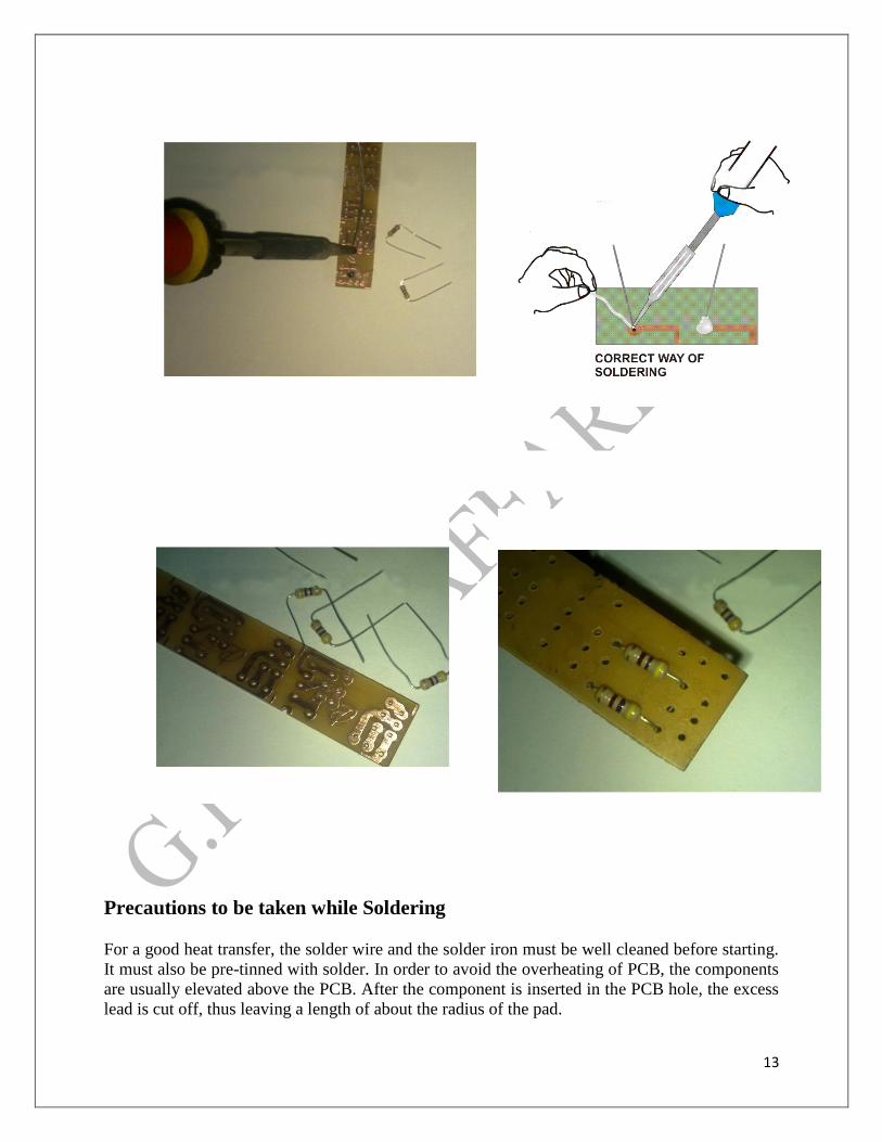
For a good heat transfer, the solder wire and the solder iron must be well cleaned before starting.
It must also be pre-tinned with solder. In order to avoid the overheating of PCB, the components
are usually elevated above the PCB. After the component is inserted in the PCB hole, the excess
lead is cut off, thus leaving a length of about the radius of the pad.

14
After soldering, the soldered joints must also be cleaned after it has been solidified.
Some components that are to be soldered may be heat sensitive. For such components a heat sink
may be used on the leads which will reduce the heat transfer to the components. The only
problem is that for such components more heat will be required from the solder iron to complete
the joint.
15
Government Polytechnic, Muzaffarpur
ELECTRONIC CONSTRUCTION AND REPAIR LAB
Subject Code: 1620407
Experiment:4
Aim: Assembling Inverter
Theory:
An inverter is a device that changes D.C. voltage into A.C. voltage. A direct current (D.C) is a
current that flows in only one direction, while an alternating current (A.C.) is that which flows in
both positive and negative directions.
The inverter performs the opposite function of a rectifier formed in the late nineteenth century
through the middle of the twentieth century; DC to AC power conversion was accomplished
using rotary converters or motor-generator sets (M-G set).
The origins of electromechanical inverters explain the source of the term inverter. Early A.C to
D.C converters used an induction or synchronous AC motor direct – connected to a generator
(dynamo) so that the generators commutator reversed its connections at exactly the right
moments to produce DC. A later development is the synchronous converter, in which the motor
and generator windings are combined into one armature, with slip rings at one end and a
commutator at the other end only one field frame.
Transformer:
It is an inductively coupled circuit used for transmitting alternating current energy. It is also used
for matching impedance between the generator and the load. It makes use of mutual inductance
in which a current flowing in a coil produces a varying electromagnetic wound over the primary
coil.
Most transformers are used to step-up or step down voltage or current. The number of turns on
the primary winding is usually different form that of Secondary. However, an isolation
transformer provides secondary voltage and current that is same as that of primary voltage and
current, because both winding have the same number of turns, (Expect for resistive losses).
These transformers prevent the transfer of unwanted electrical noise from the primary to the
secondary winding.
The primary and secondary windings of conventional transformer for electronic application are
wound on tubular bobbin (insulated spool that serves as a support for the coil) made of plastic
and other insulated materials. The wound bobbins are then enclosed by iron or steel cores in the
shape of figure start of “E” and “I” shaped laminated metal sheets, assembled through and round
16
the wound bobbins. The laminations are then clamped down to form a rigid assembly; some
transformers have plastic shrouds to insulate the windings from the core. Both primary and
secondary windings can be wound on the same bobbin, but it is now common practice, to wind
the primary and secondary windings separately on a split bobbin, to improve electrical isolation.
The primary and secondary terminals may be connected to rigid pins on the bobbin that also
functions as printed circuit board mounting pins.
Mosfet:
Metal Oxide Semiconductor Field Effect Transistor (MOSFET) is a three terminal device they
can be used either as an amplifier or as a switch. MOSFETs are classified as enhancement a
depletion types.
Battery:
It is a d.c. power source to electrical or electronic equipment or devices that make use of it.
Battery is being made available as direct source of energy. It is therefore necessary to select a
reliable battery for optimum performance.
Light Emitting Diode:
It radiates optical energy when forward biased. LED is divided into base on the type of optical
energy it radiates. The visible LED provides a useful means of indicating the state of a circuit
and is therefore used as an indicator. In order to use visible LED as an indicating there is a need for the
use of a protective resistor, which serves as a potential divider as shown below. The invisible/infrared
LED radiates infrared light when forward biased. It is used in conjunction with the photodiode
phototransistor to form a sensing system as in the remote control circuit.
2. INVERTER DESIGN AND CONSTRUCTION
The inverter is a two operation modes device, the inverting and the charging modes. The
inverting mode comprises of the oscillator, the driver, the output (MOSFET) section, the PWM
section, low battery / overload protection circuit, and the transformer. The charging mode
implements the transformer, the FET‟s (internal diodes) and the charging control circuit. A third
operation mode is the changeover modes for switching between the two aforementioned modes
at times of auto-back up for power failure and power restoration for the charging process. This
mode implements a delay circuit, electromagnetic relays and power supply circuit.
3. TRANSFORMER DESIGN
A transformer is a device that couples two AC circuits magnetically and provides electrical isolation
between the circuits while allowing a transformation of voltage and current from one circuit to another i.e.
it is mainly used for voltage and current transformation .
The Generated E.M.F in a Wounded Transformer

17
In observing an ideal transformer with secondary opened and the primary connected to a
sinusoidal alternating voltage V1, the potential different causes an alternating current to flow in
the primary since primary coil is purely inductive and has no output but draw the magnetizing
current I only .And this I will function as to magnetized the core in the secondary .It is small in
and lag voltage V1 by 900. It therefore produces an alternating flux that is proportional to the
current inputs. This flux is linked by both primary and secondary windings .Thus; this leakage(s)
produced a mutually induced e.m.f E2 in secondary winding that anti-phase with V1 and has
magnitude proportional to rate of change of flux and the number of secondary turns.
Let N1=Number of turns in primary, N2=number of turns in secondary
The transformation ratio, K= N1/N2
The equation for the voltage and current transformation of a transformer is given by K= V2/V1= I1/I2
F=Frequency of A.C input (Hz)
Maximum flux in core (Webbers) =B*A
Average rate of change of flux =maximum. Flux divided by 1/4F. (Wb/s or Volt.)
Now rate of change of flux per turn means induced e .m .f in Volt
Thus Average e.m. f /turn =4*F*max. Flux
Since the flux is sinusoidal
r.m.s =form factor*Average e.m.f /turn
But form factor =r.m.s value /Average value=1.11,
Then r.m.s value of E.m.f =1.11*4F*max. Flux =4.44F*max. Flux ,
But max .flux =Bm*A r.m.s value of E.m .f in primary turn (Tp) =4.44F*Bm*A*Tp
NOTE: Bm is assumed to be 15000Wb/m. F=50 Hz By introducing stacking factor (10-8) and Tp
factor (0.9) then we have Number of turns per volt, NT.V-1= 7/A
But form factor =r.m.s value /Average value=1.11, Then r.m.s value of E.m.f =1.11*4F*max. Flux
=4.44F*max. Flux , But max .flux =Bm*A r.m.s value of E.m .f in primary turn (Tp)
=4.44F*Bm*A*Tp NOTE: Bm is assumed to be 15000Wb/m. F=50 Hz By introducing stacking
factor (10-8) and Tp factor (0.9) then we have Number of turns per volt, NT.V-1= 7/A
4. CHOICE OF TRANSFORMER’S COMPONENTS
The power Rating for the Inverter transformer (KVA) =1.0KA , E2=12V
Assuming the efficiency of transformer =85%
Then Input rating =output /Efficiency=1000VA/0.85=1176VA
18
Ip = PI / VP VP = 260V
Ip = 1176 / 260 = 4.5A
Is = Po / Vs Vs = 12V
Ip = 1000 / 12 = 83.3A
5. 50 Hz FREQUENCY OSCILLATOR SECTION
The generation of 50 Hz frequency by the oscillator section is based on the application of a
PWM controller IC SG3524
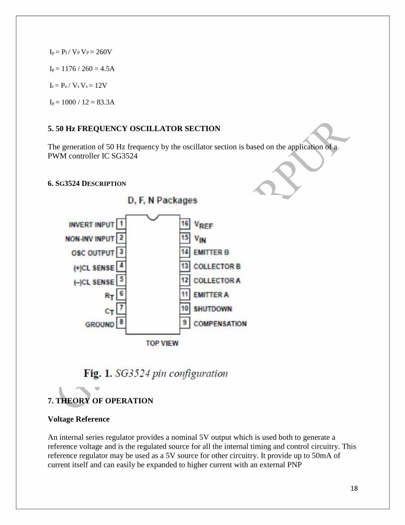
6. SG3524 DESCRIPTION
7. THEORY OF OPERATION
Voltage Reference
An internal series regulator provides a nominal 5V output which is used both to generate a
reference voltage and is the regulated source for all the internal timing and control circuitry. This
reference regulator may be used as a 5V source for other circuitry. It provide up to 50mA of
current itself and can easily be expanded to higher current with an external PNP

19
Oscillator
The oscillator in the SG3524 uses an external resistor (RT) to establish a constant charging
current into an external capacitor (CT). While this uses more current than a series-connected RC,
it provides a linear ramp voltage on the capacitor which is also used as a reference for the
comparator.
8. THE OSCILLATOR SECTION
The schematic diagram of the oscillatory section is as shown in fig. 2. IC1 SG3524 is used to
generate the 50 Hz frequency required to generate AC supply by the inverter. Battery supply is
connected to the pin-15. Pin-8 of the IC1 is connected to negative terminal of the battery. Pin-6
and 7 of IC1 are oscillator section pins.
9. DRIVER SECTION
MOS drive signal from pin-11 and 14 of IC1 are coupled to base of transistors T1 and T2. This
result in the separation of the signal into two different channels and an amplification of the signal
to a sufficient level output from the transistors emitter. The resulting MOS drive signal at emitter
of T1 and T2 is coupled to the gate of each MOSFET in the first and second MOSFET channels
respectively. The driver section made up of T1 and T2 circuit is incorporated into the oscillator
Fig 2. Oscillator Circuit Diagram
20
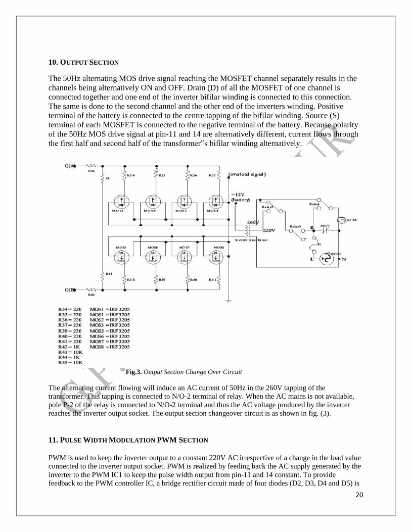
10. OUTPUT SECTION
The 50Hz alternating MOS drive signal reaching the MOSFET channel separately results in the
channels being alternatively ON and OFF. Drain (D) of all the MOSFET of one channel is
connected together and one end of the inverter bifilar winding is connected to this connection.
The same is done to the second channel and the other end of the inverters winding. Positive
terminal of the battery is connected to the centre tapping of the bifilar winding. Source (S)
terminal of each MOSFET is connected to the negative terminal of the battery. Because polarity
of the 50Hz MOS drive signal at pin-11 and 14 are alternatively different, current flows through
the first half and second half of the transformer‟s bifilar winding alternatively.
Fig.3. Output Section Change Over Circuit
The alternating current flowing will induce an AC current of 50Hz in the 260V tapping of the
transformer. This tapping is connected to N/O-2 terminal of relay. When the AC mains is not available,
pole P-2 of the relay is connected to N/O-2 terminal and thus the AC voltage produced by the inverter
reaches the inverter output socket. The output section changeover circuit is as shown in fig. (3).
11. PULSE WIDTH MODULATION PWM SECTION
PWM is used to keep the inverter output to a constant 220V AC irrespective of a change in the load value
connected to the inverter output socket. PWM is realized by feeding back the AC supply generated by the
inverter to the PWM IC1 to keep the pulse width output from pin-11 and 14 constant. To provide
feedback to the PWM controller IC, a bridge rectifier circuit made of four diodes (D2, D3, D4 and D5) is
21
connected to the drain of the MOSFET channels. The DC voltage from the bridge rectifier is filtered by a
10μF capacitor and given to pin-1 of PWM IC through a potential divider circuit made of 10k and PWM
adjustment preset VR2. The PWM circuit has also been incorporated into the oscillator schematic
diagram as shown in fig. (2). Pin-1, 2 and 9 are three pins of an internal Op-Amp, pin-1 and 2 are input
pins and pin-9 is the output pin. Pin-1 is given the feedback signal; pin-2 is given 2.5V regulated supply
as reference voltage through voltage divider circuit of two 10K resistors. The reference voltage is taken
from pin-16 of the PWM IC1. Pin-9 is internally connected to the section that controls the width of the
oscillating frequency. Change in signal at pin-9 will result in a change in the width of the output
frequency and this will always bring back the inverter output to its original 220V.
12. LOW BATTERY / OVERLOAD PROTECTION CIRCUIT
The low battery and overload protection circuit is a protection circuitry that protects the
battery from being over drain and inverter‟s transformer and MOSFET from being damaged
respectively. The low battery and overload shutdown circuit are built upon Op-Amp
comparator application.
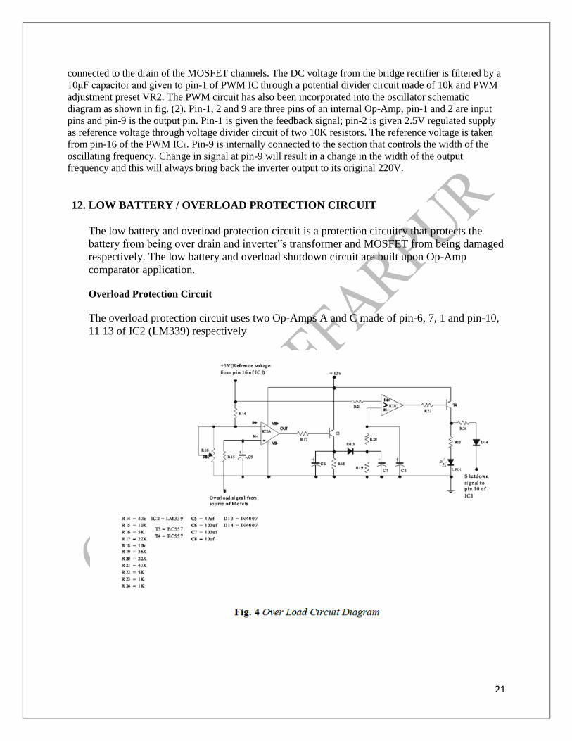
Overload Protection Circuit
The overload protection circuit uses two Op-Amps A and C made of pin-6, 7, 1 and pin-10,
11 13 of IC2 (LM339) respectively

22
Battery Charging Control Section
In this mode, the inverter transformer works as a step-down transformer and output 12V at
its secondary winding. During charging, MOSFET at the output section works as rectifier
(due to internal diodes), the drain being the cathode and the source as anode. The center
tapping of the transformer is connected to the positive terminal of the battery and the
MOSFET source is connected to negative terminal of the battery. When the inverter receives
AC mains supply, inverter transformer and MOSFET together works as a charger and
charge the battery.
The battery charging control circuit is as shown in fig. 7. In other to protect the battery from
being over charge and the MOSFET from sudden surge current at the start of charging when
power is restored, two other circuits are incorporated; the soft start section and charging
voltage sensing sections.
13. CHARGING VOLTAGE SENSING SECTION
The charging voltage sensing section makes use of Op-Amp A and B of IC3 (LM393), SCR Q2,
transistors T6 and T7. Pin-2 and 6 of IC3 is given a constant reference voltage of 5.6V through 47k
resistor. Pin-3 is given positive supply from the battery through divider circuit of 5k and 7k resistor.
When the charging battery voltage is below 12V, pin-2 voltage is higher than pin-3 voltage and thus
Op-Amp A of IC3 ramps low which biases transistor T6. The voltage at the collector of T6 provides
the trigger current IT for SCR Q2 through 1k resistor. Q2 switches ON (conduct) and 8V battery
charging signal is available at cathode used for the following;
23
Once Q2 is fired, charging continues until the voltage at pin-5 of IC3 passes a voltage level
of 5.6V when the battery is charged beyond 14.5V. At charging battery Volt of 14.5V, pin-5
of IC3 becomes more positive than pin-6 thus op-amp B ramps high to bias transistor T7.
The switching of T7 reduces the holding current IH of Q2 to zero and Q2 stops conducting.
Q2 remains in the off state until battery voltage fall below 12V when charging starts again.
Charging continues till 14.5V is reached. In this way, the battery charge is topped at interval
to keep the battery voltage level before power failure. This is incorporated in fig. 6 battery
charging control circuit.
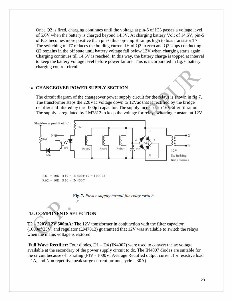
14. CHANGEOVER POWER SUPPLY SECTION
The circuit diagram of the changeover power supply circuit for the relays is shown in fig 7.
The transformer steps the 220Vac voltage down to 12Vac that is rectified by the bridge
rectifier and filtered by the 1000μf capacitor. The supply increases to 16V after filtration.
The supply is regulated by LM7812 to keep the voltage for relay switching constant at 12V.
15. COMPONENTS SELECTION
T2 – 220V/12V 500mA: The 12V transformer in conjunction with the filter capacitor
(1000uf/25V) and regulator (LM7812) guaranteed that 12V was available to switch the relays
when the mains voltage is restored.
Full Wave Rectifier: Four diodes, D1 – D4 (IN4007) were used to convert the ac voltage
available at the secondary of the power supply circuit to dc. The IN4007 diodes are suitable for
the circuit because of its rating (PIV - 1000V, Average Rectified output current for resistive load
– 1A, and Non repetitive peak surge current for one cycle – 30A)

24
Filter Capacitor: the 1000μf /25 capacitor is used to filter the ripple levels present in the
rectifier voltage. The values of the capacitor used with a 50Hz supply may range from 100uf –
30,000uf depending on the load current and the degree of smoothening required. In selecting
capacitors, the ripple voltage required is 10% of the peak value. The selection of this capacitor is
based on the following calculation.
17. PERFORMANCE EVALUATION
Table 4.1. Settings on the Inverter
Inverter output voltage
Inverter frequency
Minimum battery voltage
Maximum loading capacity
Minimum A.C. input voltage
Maximum A.C. input voltage
Table 4.2. Load Test
Power (watt)
Voltage (v)
16. MAINTENANCE, SAFETY AND PRECAUTION
1. Dead batteries should not be used with the inverter
2. The battery terminals should not be removed too often. When it is removed, replacement of
correct polarity must be ensured.
3. The inverter must be put in a moderate temperature environment.
4. The inverter should always be shut down when not in use

25
5. The inverter should always be partially loaded (not more than 80% of its maximum capacity
will be enough).
6. The use if inductive loads like refrigerator, induction machine e.t.c. on the inverter should be
avoided.
7. The input plug of the inverter should be plugged to a three-pin, properly earthed socked.
18. CONCLUSION
26
Government Polytechnic, Muzaffarpur
ELECTRONIC CONSTRUCTION AND REPAIR LAB
Subject Code: 1620407
Experiment:5
Aim:
AC Adapter Troubleshooting and Repair
AC Adapter Testing
AC adapters can easily be tested with a VOM or DMM. The voltage we measure (AC or DC)
will probably be 10-25% higher than the label specification. If we get no reading, wiggle,
squeeze, squish, and otherwise abuse the cord both at the wall wart end and at the device end.
We may be able to get it to make momentary contact and confirm that the adapter itself is
functioning.
The most common problem is one or both conductors breaking internally at one of the ends due
to continuous bending and stretching.
Make sure the outlet is live - check with a lamp.
Make sure any voltage selector switch is set to the correct position. Move it back and forth a
couple of times to make sure the contacts are clean.
If the voltage readings check out for now, then wiggle the cord as above in any case to make sure
the internal wiring is intact - it may be intermittent.
Although it is possible for the adapter to fail in peculiar ways, a satisfactory voltage test should
indicate that the adapter is functioning correctly.
It's also possible that the power jack on the device itself is damaged from use or abuse. If
possible, confirm proper operation with a COMPATIBLE adapter. With battery operated
devices, there is usually a set of contacts that should close when the adapter is removed to
connect the internal battery to the circuitry. If these don't operate properly, the device may not
work off batteries (they may appear to not be charged), the AC adapter, or both. Check the jack

27
for obvious signs of damage (cracked, loose, etc.). A squirt of contact cleaner into the jack may
clear up intermittent contact problems not due to actual damage.
AC Adapter Repair
Although the cost of a new adapter is usually modest, repair is often so easy that it makes sense
in any case.
The most common problem (and the only one we will deal with here) is the case of a broken wire
internal to the cable at either the wall wart or device end due to excessive flexing of the cable.
Usually, the point of the break is just at the end of the rubber cable guard. If we flex the cable,
we will probably see that it bends more easily here than elsewhere due to the broken inner conductor. If we are reasonably dextrous, we can cut the cable at this point, strip the wires back
far enough to get to the good copper, and solder the ends together. Insulate completely with
several layers of electrical tape. Make sure we do not interchange the two wires for DC output
adapters! (They are usually marked somehow either with a stripe on the insulator, a thread inside
with one of the conductors, or copper and silver colored conductors. Before you cut, make a note
of the proper hookup just to be sure. Verify polarity after the repair with a voltmeter.
The same procedure can be followed if the break is at the device plug end but we may be able to
buy a replacement plug which has solder or screw terminals rather than attempting to salvage the
old one.
Once the repair is complete, test for correct voltage and polarity before connecting the powered
equipment.
This repair may not be pretty, but it will work fine, is safe, and will last a long time if done
carefully.
If the adapter can be opened - it is assembled with screws rather than being glued together - then
we can run the good part of the cable inside and solder directly to the internal terminals. Again,
verify the polarity before we plug in our expensive equipment.
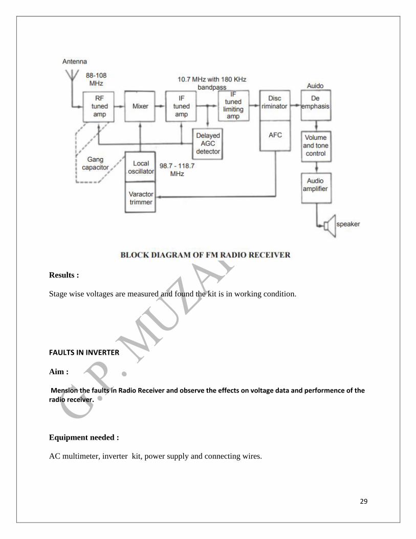
FAULTS IN RADIO RECEIVER
Aim :
Mension the faults in Radio Receiver and observe the effects on voltage data and performence of the radio receiver.
Equipment needed :

28
AC multimeter, radio receiver kit, power supply and connecting wires.
Theory & Procedure :
General faults identified in radio receiver as follows
1. low sound of Radio Band
2. Shortwave working but MW is not working
3. Disturbed and booming sound of radio band
4. Normal sound at low volume level, but distorted output when volume increases.
5. AM band is not working
1. Low Sound of Radio Band :
Due to misalignment of IFTs and related stages components detection diode (OA79) and related
components loose contact or dry solder, check print.
2. SW working but MW is not working :
This problems occurs when band switch point open at MW band position. Properly contact
position should be adjusted to switch position, MW oscillator, MW antenna coil open, moisture
on MW oscillator coil, loose contact or dry solder, check print of PCB.
3. Disturbed and booming sound of Radio Band :
This problem comes when gang capacitor is connected loosly, trimmer loose, band switch loose,
oscillator crip or IFT instable or loose contact or dry solder, check print of PCB.
4. Normal sound at low volume level, but distorted output when volume increases :
Low supply voltage or low current, check for excess to motor, high tension in pinch roller, belt is
tight rectifing and filter circuit components failure, weak motor, loose cantact, dry solder, check
print, low sound occurs for defects.
5. AM band is not working :
Defects in coils and gang capacitor, select switch S1 defective band switch, loose contact or dry
solder, check print of PCB.
29
Results :
Stage wise voltages are measured and found the kit is in working condition.
FAULTS IN INVERTER
Aim :
Mension the faults in Radio Receiver and observe the effects on voltage data and performence of the radio receiver.
Equipment needed :
AC multimeter, inverter kit, power supply and connecting wires.

30
Inverter
Theory & Procedure :
If the inverter appear to be malfunction following procedure should be followed to eliminate any
external problems.
1.Turn the Inverter “OFF” via the circuit breaker switch on the front panel.
1. Disconnect all AC wiring from the Inverter.
2. Disconnect DC Battery leads from Battery.
3. Clean Terminals (remove all grease and or corrosion on both DC leads and battery terminals

31
4. Ensure we have sufficient battery capacity at the nominal voltage (specified on the
compliance label at the rear of our Inverter). Please note: Use minimum 60AH battery or the
size of a substantial car battery.
5. Make connection direct to battery terminals and insure all connections are tight.
6. Ensure battery voltage is within the correct limits as outlined in the section ELECTRICAL &
MECHANICAL SPECIFICATIONS of this manual. If we do not have a DC voltmeter or
multimeter check the front panel for overvolts and undervolts LED’S.
7. Turn the Inverter “ON” via the circuit breaker switch on the front panel. Observe the lights
on the front left of your Inverter. Refer to sections INVERTER OPERATION for
explanation of lights and / or section FAULT FINDING CHART.
8. Plug in various appliances and monitor the Inverters operation.
Important must be remembered
• Remember that it has automatic start with load.
• Make sure leads and terminals are not corroded or faulty in any way.
• Make sure the Inverter goes into Standby with no load switched on.
• Make sure the circuit breaker is reset properly. If unsure switch “OFF” and “ON” again.
• When measuring the AC output of Modified Squarewave Inverters use a TRUE RMS VOLT
METER. Average reading meters will not give an accurate measurement. (240V RMS =
210V average) depending on Battery voltage and load

32
Symptom Cause a
Action
No LED on. Is Circuit Breaker switched on? Switch OFF and ON.
No output power. Is input voltage present? Check battery connections.
Was too high DC Voltage left on Inverter ie. from PV If voltage exceeds more than triple the Inverter input voltage, damage
Modules or battery charger may have occurred.
Inverter does not go back to Stand by Inverter senses load present.
Disconnect all loads. Disconnect leads on junction box on back of
mode Green LED does not Inverter.
flash. Auto Start set too low. Turn Auto Start clockwise.
Inverter overloads constantly. Inverter overheated due to a large load being run. Check if case is hot, allow 5 minutes to cool down, reset Inverter via
circuit breaker.
Current draw from battery is excessive due to a short Disconnect all AC 240V wiring from Inverter, check if Green LED
circuit on 240V AC side or load to be started is too flashes .
large.
Fluorescent Lights are used with power factor Remove capacitors (MSW only)
correction capacitors
If any lightning has occurred unit might be damaged. Return to supplier.
Inverter constantly shuts down in Battery voltage below specified limit. Check battery connections and state of charge (should be above SG
undervolts. level of 1220)
Battery voltage drops below limit only when load is Check size of load, might be too large for battery to handle. Check
being connected. connections! Check DC wiring between Inverter and battery for any
defects!
Inverter constantly shuts down in Battery voltage above specified limit. Battery might be overcharged.
overvolts. Battery charger imposes high ripple peak voltages Check battery charger.
across battery terminal which may exceed limit for short periods.
Solar panels are connected to Inverter without Open circuit voltage of solar panels exceeds limit. Check system.
batteries.
Solar regulator causes voltage peaks across battery Check solar regulator for this symptom. This only occurs during peak
terminals. sun periods and when load demand on system is very low, ie. during
holiday periods.
Battery Charger without regulation circuit and or choke
Battery bank might be too small to soak up these currents. The
is connected to the battery which imposes very high detection circuit of the Inverter works within a time frame of 0.1 second
peak currents. to detect this fault condition. Check float voltage.

33
Symptom Cause Action
Inverter does not sense load Load too small for inverter to
sense. I/e. compact
Adjust Auto Start anti clockwise or run other load at the same time or
fit
(MSW only) fluros without electronic ballast! PTC Sense resistor. Use PL
lamps.
Inverter switches on with load but Current draw of load changes. ie.
small battery
Auto Start also depends on battery voltage to some extent.
Run other
drops out occasionally. chargers. small load at the same time.
Inverter starts up correctly ie. Green
Current flow causes voltage drop on Battery
Check battery connections and fuse connections. Connect
inverter
light on then flashing; but shuts connections. straight to battery terminal.
down when load applied
AC Output voltage too low Average reading meters will not
give an accurate Use TRUE RMS volt meter..(MSW only)
measurement of Modified
Squarewaves. (240V RMS =
210V average) depending on
Battery voltage and load
Conclusion:

34
Government Polytechnic, Muzaffarpur
ELECTRONIC CONSTRUCTION AND REPAIR LAB
Subject Code: 1620407
Experiment:6
Aim: Location of faults in different types of Electronics Circuits.
Apparatus :
Digital Multimeter
Analog Multimeter
ohms meter
flyback tester
Theory: While many digital multimeters these days have a specific capability for testing diodes
and sometimes transistors, not all do, especially the older analogue multimeters that are still in
widespread use. However it is still quite easy to perform a simple go / no-go test using the
simplest of equipment.
This form of testing is able to detect whether transistor or a diode is operational, and although it
cannot provide details of the parameters, this is seldom a problem because these components will
have been tested at manufacture and it is comparatively rare for the performance to fall to a point
where they do not operate in a circuit. Most failures are catastrophic, rendering the component
completely inoperable. These simple multimeter tests are able to detect these problems very
quickly and easily.
Procedure:
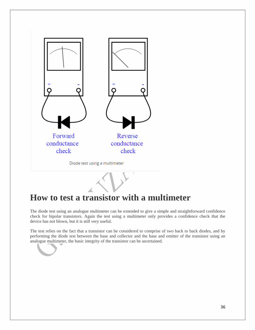
The basic diode test is very simple to perform. Just two tests are needed with the multimeter to ensure that the
diode works satisfactorily:
35
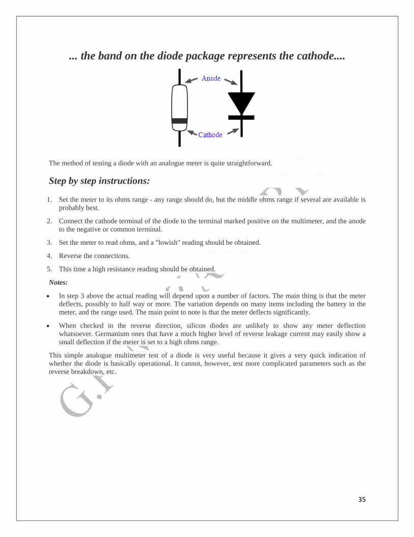
... the band on the diode package represents the cathode....
The method of testing a diode with an analogue meter is quite straightforward.
Step by step instructions:
1. Set the meter to its ohms range - any range should do, but the middle ohms range if several are available is
probably best.
2. Connect the cathode terminal of the diode to the terminal marked positive on the multimeter, and the anode
to the negative or common terminal.
3. Set the meter to read ohms, and a "lowish" reading should be obtained.
4. Reverse the connections.
5. This time a high resistance reading should be obtained.
Notes:
In step 3 above the actual reading will depend upon a number of factors. The main thing is that the meter
deflects, possibly to half way or more. The variation depends on many items including the battery in the
meter, and the range used. The main point to note is that the meter deflects significantly.
When checked in the reverse direction, silicon diodes are unlikely to show any meter deflection
whatsoever. Germanium ones that have a much higher level of reverse leakage current may easily show a
small deflection if the meter is set to a high ohms range.
This simple analogue multimeter test of a diode is very useful because it gives a very quick indication of
whether the diode is basically operational. It cannot, however, test more complicated parameters such as the
reverse breakdown, etc.
36
How to test a transistor with a multimeter
The diode test using an analogue multimeter can be extended to give a simple and straightforward confidence
check for bipolar transistors. Again the test using a multimeter only provides a confidence check that the
device has not blown, but it is still very useful.
The test relies on the fact that a transistor can be considered to comprise of two back to back diodes, and by
performing the diode test between the base and collector and the base and emitter of the transistor using an
analogue multimeter, the basic integrity of the transistor can be ascertained.
37
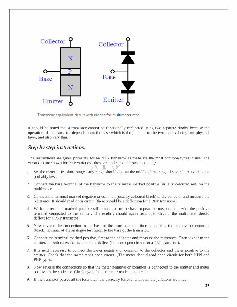
It should be noted that a transistor cannot be functionally replicated using two separate diodes because the
operation of the transistor depends upon the base which is the junction of the two diodes, being one physical
layer, and also very thin.
Step by step instructions:
The instructions are given primarily for an NPN transistor as these are the most common types in use. The
variations are shown for PNP varieties - these are indicated in brackets (.. .. ..):
1. Set the meter to its ohms range - any range should do, but the middle ohms range if several are available is
probably best.
2. Connect the base terminal of the transistor to the terminal marked positive (usually coloured red) on the
multimeter
3. Connect the terminal marked negative or common (usually coloured black) to the collector and measure the
resistance. It should read open circuit (there should be a deflection for a PNP transistor).
4. With the terminal marked positive still connected to the base, repeat the measurement with the positive
terminal connected to the emitter. The reading should again read open circuit (the multimeter should
deflect for a PNP transistor).
5. Now reverse the connection to the base of the transistor, this time connecting the negative or common
(black) terminal of the analogue test meter to the base of the transistor.
6. Connect the terminal marked positive, first to the collector and measure the resistance. Then take it to the
emitter. In both cases the meter should deflect (indicate open circuit for a PNP transistor).
7. It is next necessary to connect the meter negative or common to the collector and meter positive to the
emitter. Check that the meter reads open circuit. (The meter should read open circuit for both NPN and
PNP types.
8. Now reverse the connections so that the meter negative or common is connected to the emitter and meter
positive to the collector. Check again that the meter reads open circuit.
9. If the transistor passes all the tests then it is basically functional and all the junctions are intact.
38
Notes:
The final checks from collector to emitter ensure that the base has not been "blown through". It is
sometimes possible that there is still a diode present between collector and base and the emitter and the
base, but the collector and emitter are shorted together.
As with the germanium diode, the reverse readings for germanium transistors will not be as good as for
silicon transistors. A small level of current is allowable as this results from the presence of minority
carriers in the germanium.
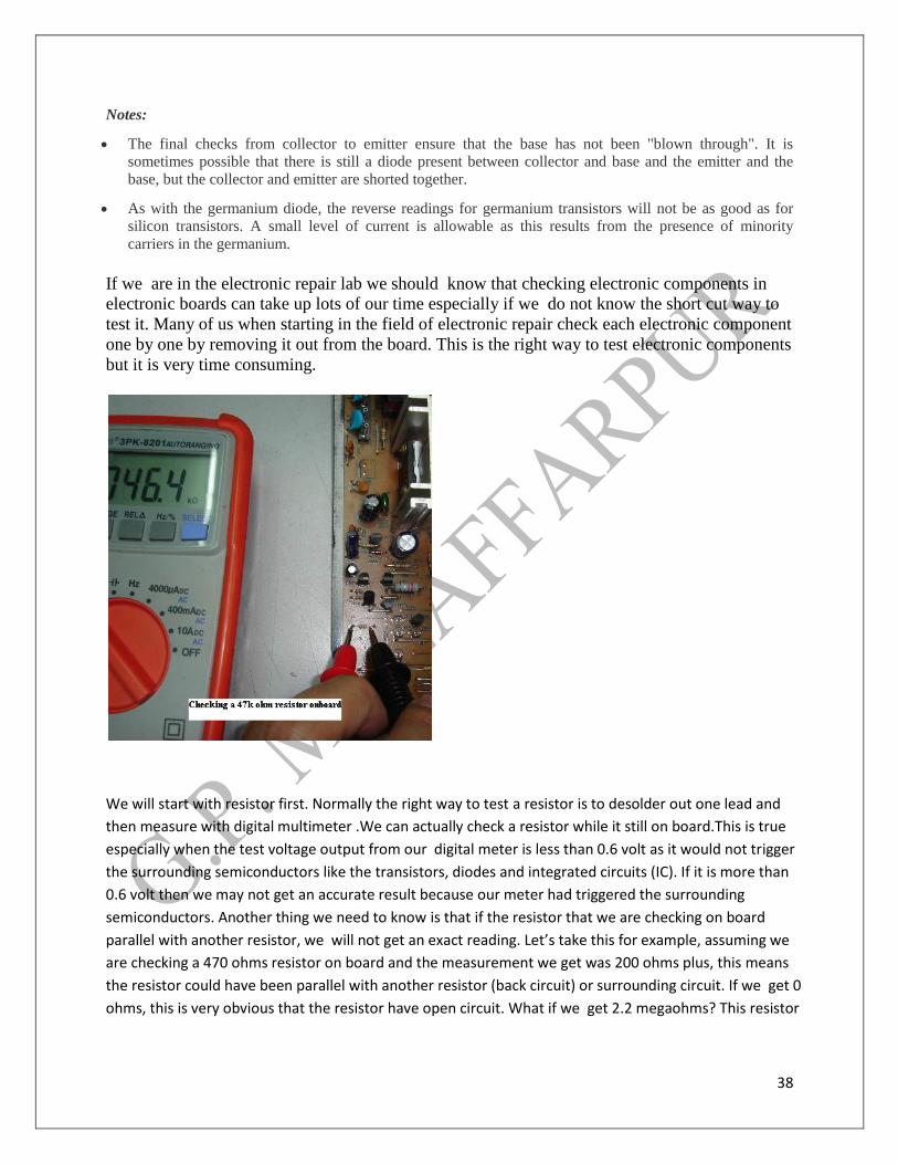
If we are in the electronic repair lab we should know that checking electronic components in
electronic boards can take up lots of our time especially if we do not know the short cut way to
test it. Many of us when starting in the field of electronic repair check each electronic component
one by one by removing it out from the board. This is the right way to test electronic components
but it is very time consuming.
We will start with resistor first. Normally the right way to test a resistor is to desolder out one lead and
then measure with digital multimeter .We can actually check a resistor while it still on board.This is true
especially when the test voltage output from our digital meter is less than 0.6 volt as it would not trigger
the surrounding semiconductors like the transistors, diodes and integrated circuits (IC). If it is more than
0.6 volt then we may not get an accurate result because our meter had triggered the surrounding
semiconductors. Another thing we need to know is that if the resistor that we are checking on board
parallel with another resistor, we will not get an exact reading. Let’s take this for example, assuming we
are checking a 470 ohms resistor on board and the measurement we get was 200 ohms plus, this means
the resistor could have been parallel with another resistor (back circuit) or surrounding circuit. If we get 0
ohms, this is very obvious that the resistor have open circuit. What if we get 2.2 megaohms? This resistor
39
is either open or has gone up in value. Other circuit components cannot possibly increase the value of a
resistor; any back circuit could only make the resistance reading lower!
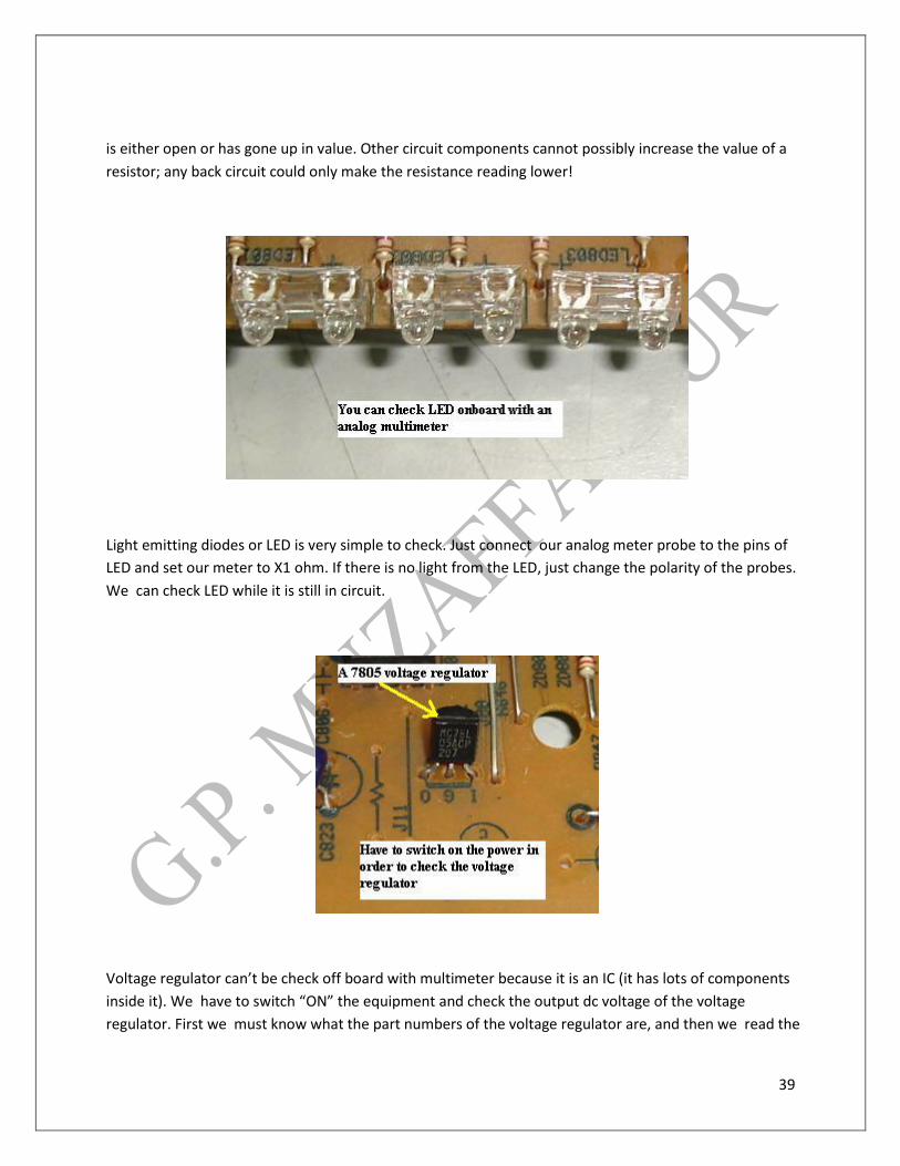
Light emitting diodes or LED is very simple to check. Just connect our analog meter probe to the pins of
LED and set our meter to X1 ohm. If there is no light from the LED, just change the polarity of the probes.
We can check LED while it is still in circuit.
Voltage regulator can’t be check off board with multimeter because it is an IC (it has lots of components
inside it). We have to switch “ON” the equipment and check the output dc voltage of the voltage
regulator. First we must know what the part numbers of the voltage regulator are, and then we read the

40
specification and locate the input and output voltage and pins. For example, the general type of voltage
regulator starts with the part numbers like 7805, 7812, 7908 and etc. From the spec we would know that
pin one is input, pin 2 is ground and pin 3 is output. If there is input voltage to the voltage regulator and
no or low output voltage, suspect the voltage regulator itself faulty or something along the output line
that dragged down the output voltage.
Many switch mode power supply are using the combination of a power FET and a PWM IC design to
switch the power transformer. Whenever there is any power failure (fuse totally blown into dark color)
one will always suspect the power FET has gave way. Usually we would use the black probe set to X 1
ohms and place it to the center pin (drain) and the red probe to the gate and the source pin. This is the
same way when we want to check HOT on board. If there is a reading, chances are high that the FET has
developed a short circuit. But we also have to remember that a shorted bridge rectifier may cause the
power FET to have reading when check with the analog meter while it still on board.
41
If we get an open reading this doesn’t mean the power FET is good because a faulty FET can become
open circuit too.We don’t waste our time checking FET onboard (if the FET shorted then we can detect
right away but what if the FET open circuit?) because it is not accurate, we have no choice when comes to
testing FET, we just have to remove it out from board and test it with analog meter set to X 10k ohms.
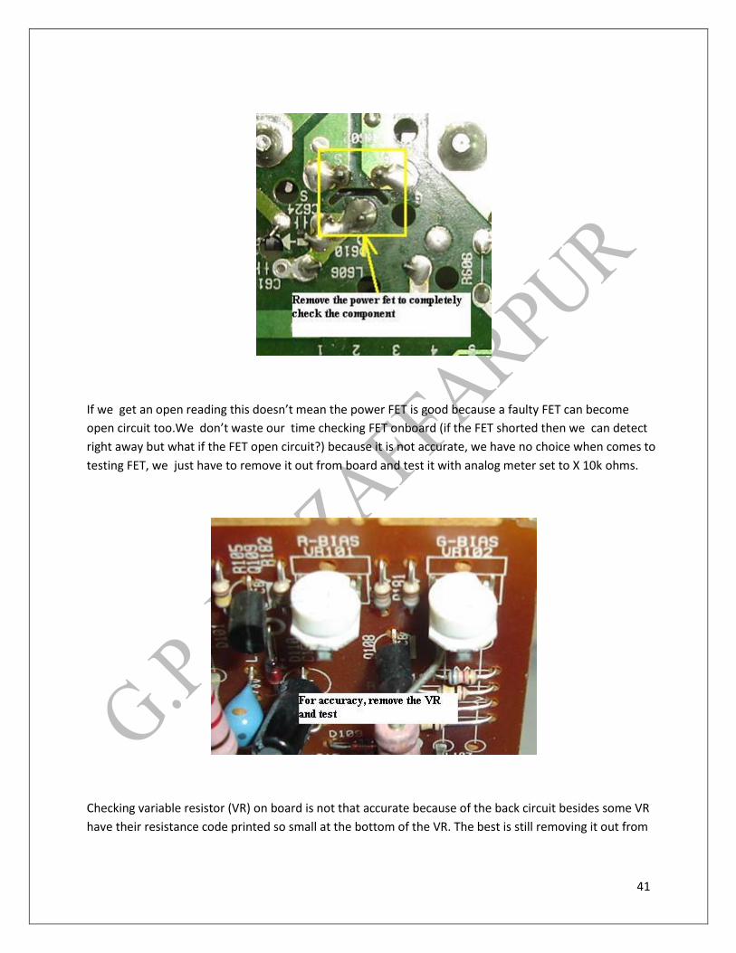
Checking variable resistor (VR) on board is not that accurate because of the back circuit besides some VR
have their resistance code printed so small at the bottom of the VR. The best is still removing it out from
42
the circuit and test it with an analog meter. Any erratic reading can be easily seen from the analog meter
panel compares to using digital meter.
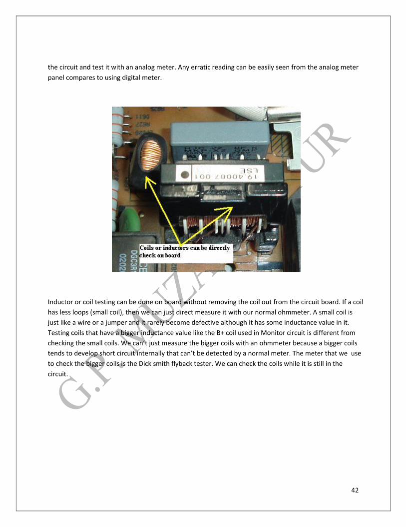
Inductor or coil testing can be done on board without removing the coil out from the circuit board. If a coil
has less loops (small coil), then we can just direct measure it with our normal ohmmeter. A small coil is
just like a wire or a jumper and it rarely become defective although it has some inductance value in it.
Testing coils that have a bigger inductance value like the B+ coil used in Monitor circuit is different from
checking the small coils. We can’t just measure the bigger coils with an ohmmeter because a bigger coils
tends to develop short circuit internally that can’t be detected by a normal meter. The meter that we use
to check the bigger coils is the Dick smith flyback tester. We can check the coils while it is still in the
circuit.
43
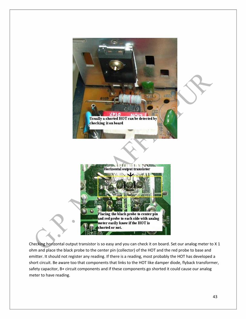
Checking horizontal output transistor is so easy and you can check it on board. Set our analog meter to X 1
ohm and place the black probe to the center pin (collector) of the HOT and the red probe to base and
emitter. It should not register any reading. If there is a reading, most probably the HOT has developed a
short circuit. Be aware too that components that links to the HOT like damper diode, flyback transformer,
safety capacitor, B+ circuit components and if these components go shorted it could cause our analog
meter to have reading.
44
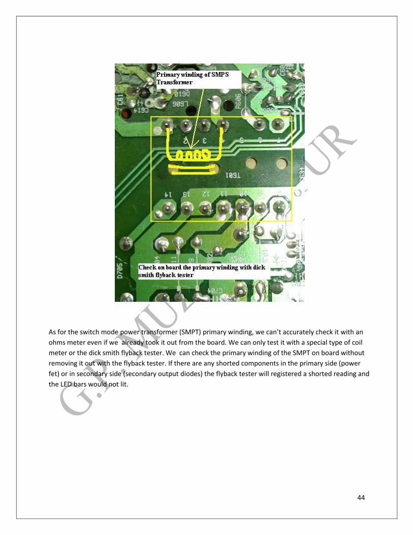
As for the switch mode power transformer (SMPT) primary winding, we can’t accurately check it with an
ohms meter even if we already took it out from the board. We can only test it with a special type of coil
meter or the dick smith flyback tester. We can check the primary winding of the SMPT on board without
removing it out with the flyback tester. If there are any shorted components in the primary side (power
fet) or in secondary side (secondary output diodes) the flyback tester will registered a shorted reading and
the LED bars would not lit.

45
Checking the on/off power switch is the easiest one. Just place our meter probes to the switch point
(assuming the power switch have 2 leads) and set our ohm meter or continuity check function. It should
show a very low ohm resistance or the beeper will beep if we use the continuity checker. We can perform
this test even if the power switch is still in circuit. We can also use this method to test on the micro
switch.

46
Optoisolator or optocoupler IC’s usually located in between the primary and secondary side of power
supply and can be test even if the IC is still on board (you can actually test this type of IC with your
multimeter). Some of the famous optocoupler part numbers are 4N25, 4N35, PC123 and etc. Just
desolder one pin on each side (assuming this optocoupler have 2 pins on each side) of the optocoupler.
Pin 1 and 2 is the LED light and pin 3 and 4 is the phototransistor collector and emitter. Place your analog
meter probe set to X10 k ohms at pin 1 and 2 either way and it should show only one reading (low
resistance reading). This is just the exact same way as when you are checking a normal diode. If it shows 2
reading most probably it had developed a short circuit. Now place your probes to pin 3 and 4 either way
and again it will only show one reading (this time the resistance reading is a little bit high). If you got two
readings then the internal transistor may have short circuit.

47
If we want to measure an optocoupler that have 6 or even 8 pins, then we have to search for its data first
from the internet or from semiconductor data book. Once we know how the internal components are
wired, then we will use the best checking method to test them individually. Remember, a shorted
optoisolator can cause low power, no power or even power blink in switch mode power supply.
Results:
Conclusion:

48
Government Polytechnic, Muzaffarpur
ELECTRONIC CONSTRUCTION AND REPAIR LAB
Subject Code: 1620407
Experiment:7
Aim:
Tracing fault in a CRO and its repair.
Troubleshooting Technique & Procedure:
The oscilloscope is an excellent tool for providing clues to faults within itself .In addition to the
CRT display,the calibrate signals and the front – panel indicators often provides sufficient
information to isolate the problem.
For effective troubleshooting ,examine the simple possibilities before proceeding with extensive
troubleshooting.The following list provides a logical sequence to follow while troubleshooting .
1. Check Control setting
2. Check associate equipment
3. Make a thorough visual check of the instrument.
4. Check instrument calibration
5. Isolate trouble to block level.
6. Check voltage & waveform
7. Check individual components.
Observing the malfunction of different multifunction switch position can do much to identify a
problem. Detecting a problem in all circuits may indicate the problem in the power supply .
Switching to the external horizontal input (X-Y mode) disconnect the sweep and is a mean of
determining whether a problem is associated with the horizontal amplifier or sweep generator.At
the same time it indicate the condition of unblinking circuitry.
Varying the trigger source switch between internal & external triggering checks the trigger pivk
off circuitry. If the sweep is free run by adjusting the stability and trigger level control ,addition
circuitry may be checked .comparing operation in different trigger modes can often localize a
problem to specific trigger modes.

49
Vertical preamplifier plug in units are quick way of checking performance to the vertical
amplifier input .Once a problem is isolated to specific plug in unit ,plug in circuit board (if used)
may isolate the problem even further.
Once a problem has been traced to a specific block ,a close visual check may pin point the
problem .Troubleshooting job can be shortened by finding the burned components and loose
leads.
Another method of streamlining troubleshooting procedure is through the substitution
method.This method can be used in many levels of troubleshooting .In troubleshooting
instruments in plug in module isolate the faulty sub-system by substituting known good plug in
modules for those that are questionable.
There are some basic rules that we must remember & follow in using this method of
troubleshooting .
1. Ensure that we use the proper components ,by part number ,when substituting .
2. Ensure that power is removed when making the substitution ,to prevent damage to the
instruments.
3. Be careful when removing and replacing components to avoid physical /mechanical
damage to the components.
4. Keep the no. of components to be minimum ,substitute one components at one time.
5. Though several components in a circuit may have same part number ,avoid inter circuit
components swaps.Failure to return components to proper place whining a circuit may
require a complete calibration of circuit.If the components are placed properly ,circuit
may require only a performance check and spot calibration after the repair is competed .
6. Always return components to proper place after the problem has been solved.

50

51
Common Power Supply problem
1.Fuse blows when power is applied –shorted diode in bridge ,shorted filter cap.
2.Fuse blows after delay-overloaded output.
3.Excessive ripple –divide by 10 for approximate solid state value.
a.50 mv to 1.5 v-comparator ,speedup capacitor
b.1.5-8 V-output filter
c.8 V to more-input filter
4. off tolerance –Leaky speedup capacitor
5. Noisy output-poor connection,noisy diode ,noisy resistor

52

53
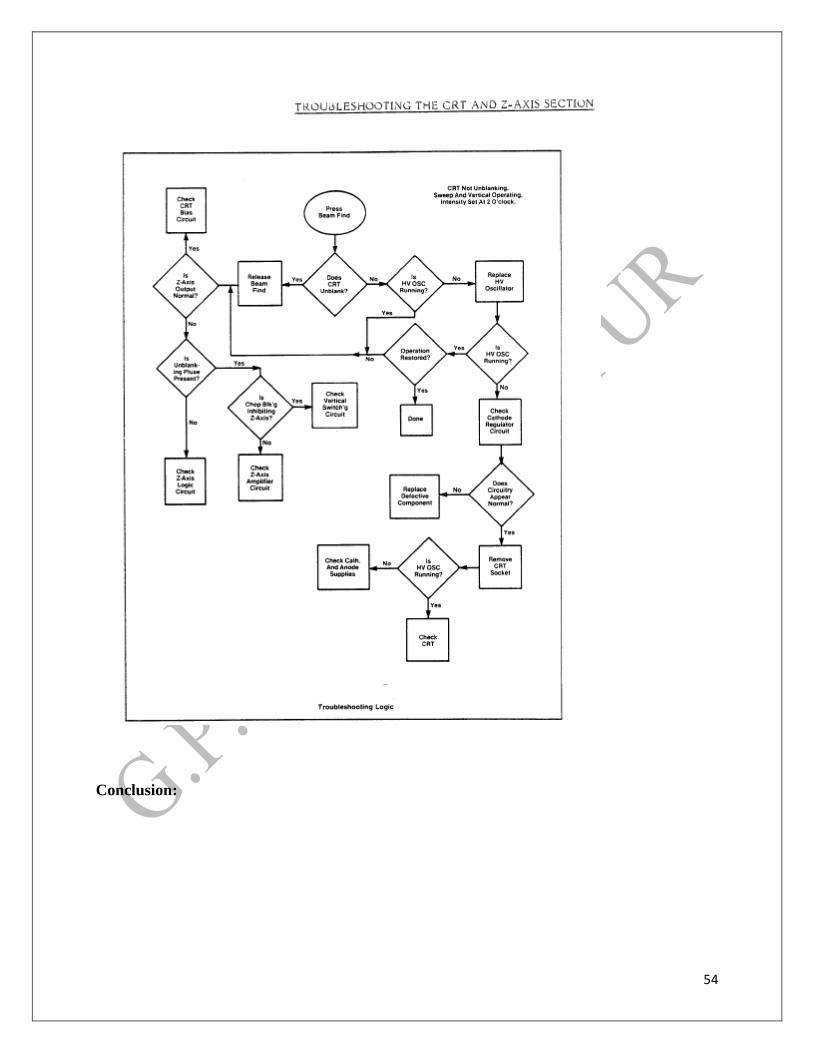
54
Conclusion:
55
Government Polytechnic, Muzaffarpur
ELECTRONIC CONSTRUCTION AND REPAIR LAB
Subject Code: 1620407
Experiment:8
Aim
Handling of different types of multimeter: Frequency meters
Theory:
Digital frequency meter is a general purpose instrument that displays the frequency of a periodic
electrical signal to an accuracy of three decimal places. It counts the number events occurring
within the oscillations during a given interval of time. As the preset period gets completed, the
value in the counter display on the screen and the counter reset to zero. Various types of
instruments are available which operates at a fixed or variable frequency. But if any frequency
meter operates at a different frequency than specified range, it could carry out abnormally. For
measuring low frequencies, the deflection type meters are widely used. The deflection of the
pointer on the scale shows the change in frequency. The deflection type instruments are of two
types: one is electrically resonant circuits and other is ratio meter.
Operating Principle of Digital Frequency Meter
A frequency meter has a small device which converts the sinusoidal voltage of the frequency into
a train of unidirectional pulses. The frequency of input signal is the displayed count, averaged
over a suitable counting interval out of 0.1, 1.0, or 10 seconds. These three intervals repeat
themselves sequentially. As the ring counting units resets, these pulses pass through the time-

56
base-gate and then entered into the main gate, which opens for a certain period of time interval.
The time base gate prevents a divider pulse from opening the main gate during the display time
interval. The main gate acts as a switch when the gate is open, pulses are allowed to pass. When
the gate is closed, pulses are not allowed to pass that means the flow of pulses get obstructed.
The functioning of the gate is operated by the main-gate flip-flop. An electronic counter at the
gate output that counts the number of pulses passed through the gate while it was open. As the
next divider pulse is received at main gate flip-flop, the counting interval ends and divider pulses
are locked out. The resultant value displayed on a display screen which has the ring counting
units of scale-of-ten circuits and each unit is coupled to a numeric indicator, which provides the
digital display. As the reset pulse generator is triggered, ring counters get reset automatically and
the same procedure starts again.
The range of modern digital frequency meter is between the range from104 to 109 hertz. The
possibility of relative measurement error ranges between from 10-9 to 10-11 hertz and a sensitivity
of 10-2 volt.
Use of Digital Frequency Meter
For testing radio equipment
Measuring the temperature, pressure, and other physical values.
Measuring vibration, strain
Measuring transducers
Vacuum Tube Voltmeter (VTVM)

57
Theory
The voltmeter which uses the vacuum tube for amplifying the measurand AC and DC
voltage is known as the vacuum tube voltmeter (VTM). The vacuum tube increases the
sensitivity of the voltmeter because of which it can detect the signal of very weak strength.
The electronic voltmeter is used for measuring the voltage of direct, RMS and peak voltage
of the system. The vacuum tube has many advantages like they have high input impedance, wide
frequency range and high sensitivity.
The most significant advantage of the VTM is that it can draw very less current as compared
to the other meter. In VTM, the measuring signal is directly supplied to the vacuum tube of the
meter. The vacuum tube is amplifying the signal and pass it to the deflecting meter.
Types of Vacuum tube Voltmeter
The Vacuum Tube Voltmeter is classified into the following types.
1. Diode Type
o Peak Reading Diode Vacuum Tube Voltmeter
2. Single Triode
3. Balanced Triode Type
4. Rectifiers Amplifier Type
5. Amplifier Rectifier Type
Simple Diode Type Voltmeter
The circuit of the diode voltmeter consists the PMMC meter, load resistor, vacuum tube diode.
The vacuum tube diode connects in series with resistance raises the strength of the weak signal.
Because of the vacuum tube, the system becomes more sensitive than the normal voltmeter.
For obtaining the accurate reading from the voltmeter, it is essential that their current and
voltage are directly proportional to each other. This can be done by the help of the series
resistor. The circuit diagram of the diode vacuum tube voltmeter is shown in the figure below.
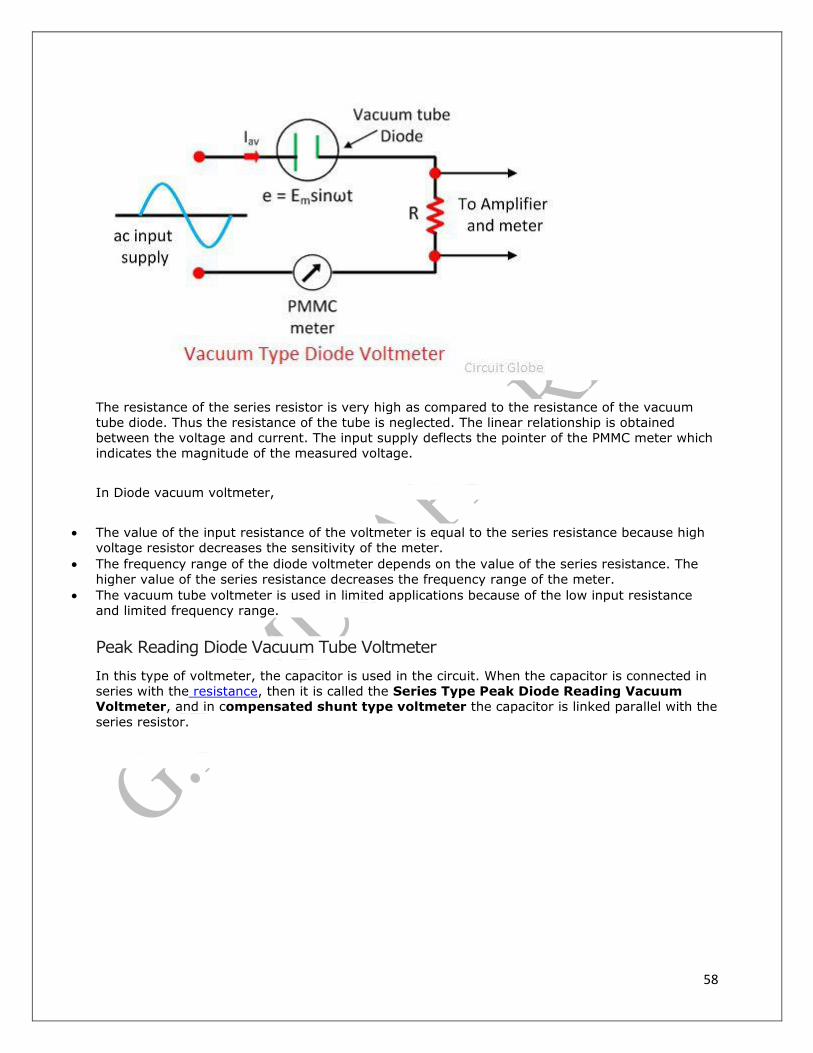
58
The resistance of the series resistor is very high as compared to the resistance of the vacuum
tube diode. Thus the resistance of the tube is neglected. The linear relationship is obtained
between the voltage and current. The input supply deflects the pointer of the PMMC meter which
indicates the magnitude of the measured voltage.
In Diode vacuum voltmeter,
The value of the input resistance of the voltmeter is equal to the series resistance because high
voltage resistor decreases the sensitivity of the meter.
The frequency range of the diode voltmeter depends on the value of the series resistance. The
higher value of the series resistance decreases the frequency range of the meter.
The vacuum tube voltmeter is used in limited applications because of the low input resistance
and limited frequency range.
Peak Reading Diode Vacuum Tube Voltmeter
In this type of voltmeter, the capacitor is used in the circuit. When the capacitor is connected in
series with the resistance, then it is called the Series Type Peak Diode Reading Vacuum
Voltmeter, and in compensated shunt type voltmeter the capacitor is linked parallel with the
series resistor.
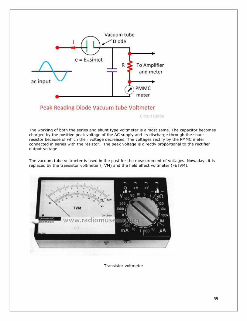
59
The working of both the series and shunt type voltmeter is almost same. The capacitor becomes
charged by the positive peak voltage of the AC supply and its discharge through the shunt
resistor because of which their voltage decreases. The voltages rectify by the PMMC meter
connected in series with the resistor. The peak voltage is directly proportional to the rectifier
output voltage.
The vacuum tube voltmeter is used in the past for the measurement of voltages. Nowadays it is
replaced by the transistor voltmeter (TVM) and the field effect voltmeter (FETVM).
Transistor voltmeter
60
FETVM-FET Voltmeter
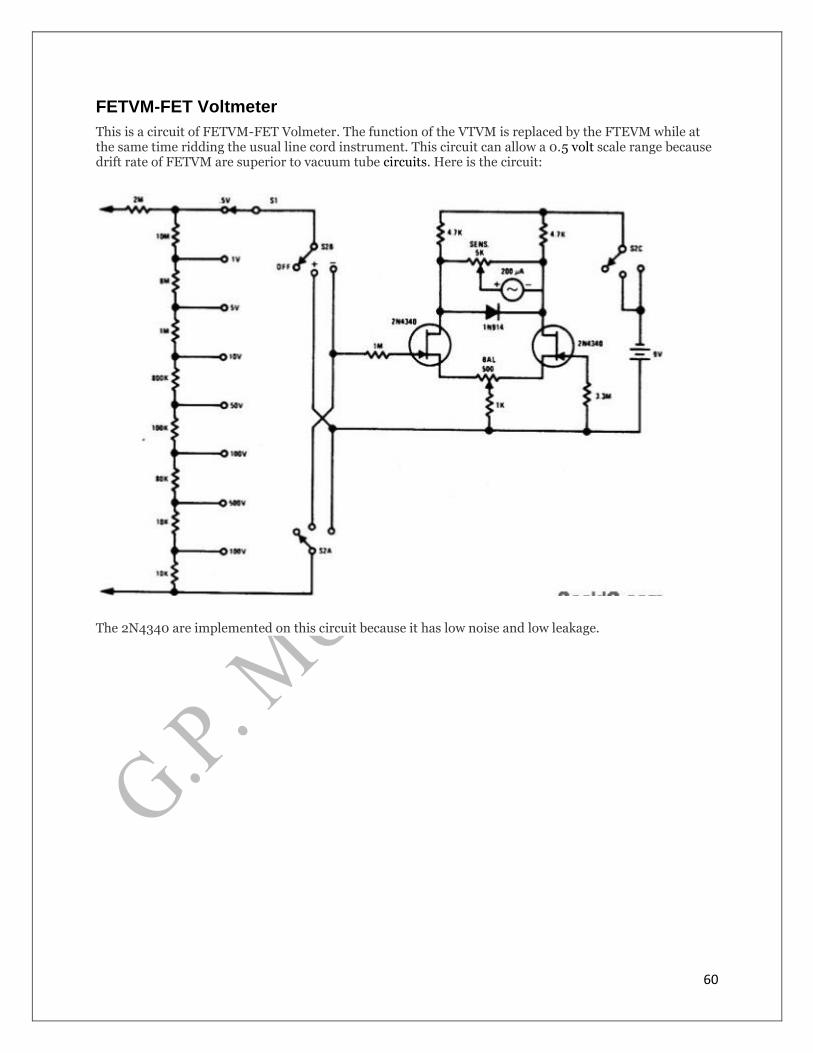
This is a circuit of FETVM-FET Volmeter. The function of the VTVM is replaced by the FTEVM while at the same time ridding the usual line cord instrument. This circuit can allow a 0.5 volt scale range because drift rate of FETVM are superior to vacuum tube circuits. Here is the circuit:
The 2N4340 are implemented on this circuit because it has low noise and low leakage.
61
v
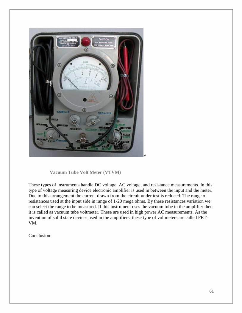
Vacuum Tube Volt Meter (VTVM)
These types of instruments handle DC voltage, AC voltage, and resistance measurements. In this
type of voltage measuring device electronic amplifier is used in between the input and the meter.
Due to this arrangement the current drawn from the circuit under test is reduced. The range of
resistances used at the input side in range of 1-20 mega ohms. By these resistances variation we
can select the range to be measured. If this instrument uses the vacuum tube in the amplifier then
it is called as vacuum tube voltmeter. These are used in high power AC measurements. As the
invention of solid state devices used in the amplifiers, these type of voltmeters are called FET-
VM.
Conclusion:
62
Government Polytechnic, Muzaffarpur
ELECTRONIC CONSTRUCTION AND REPAIR LAB
Subject Code: 1620407
Experiment:9
Fault Location and repair of instruments – Multimeter
Aim: Transistor Circuit Test & Fault Finding using a Multimeter
Procedure for fault finding :
One of the main uses for multimeters whether they are analogue multimeters or digital
multimeters, DMMs is to test and fault find circuits like those in a transistor radio. Multimeters
are ideal items of test equipment for finding many faults in a transistor circuit.
However to use a multimeter to test a circuit and find faults it is necessary to have a little
knowledge about the circuit, and also to adopt a logical approach in tracking down any faults that
may exist.
The first step when looking at tracing any faults and testing a transistor circuit of any sort is to
look for the obvious or major faults. Fortunately most faults with electronics equipment such as
transistor radios are relatively major and therefore easy to find. Accordingly the first step in any
fault finding is to look for the major problems.
1.Check the supply to the circuit: The first steps in checking the circuit are to ensure that it
has power being supplied to it. This is easily done using a multimeter set to a voltage range.
Measure the voltage using a multimter at the points where the supply enters the circuit board. If
the multimeter indicates that there is no supply voltage then there can be a number of
possibilities to investigate.

63
1.Battery could be flat if the equipment is battery powered
2.If the transistor equipment is battery powered, the battery could have been left in for many
months and corroded the battery compartment. Check for this and if there are signs of leakage
then clean and remove all signs of corrosion being careful not to touch any of the residue.
3.On-off switch faulty. This can be checked by disconnecting any power source and checking for
continuity across the switch
4.Corroded connector. One common problem is that connectors become corroded with time and
connections can become very poor, especially of the equipment has not been used for some time.
To overcome this it can help to unplug and then re-mate the connector.
5.Check for any broken wiring that would prevent the power reaching the circuit board
2.Check the outputs from the board: In the same way that broken connections may exist for
the power line, the same may be true of the outputs from the board. Again it is worth checking
any connectors that may have corroded or oxidised with time, and check for any broken
connections.
3.Check the inputs to the circuit: Likewise, if the signal inputs are not reaching the board then
it will not be able to perform. Again any switches, and connectors along with any broken wires
should be checked. Often a multimeter can be used to check the continuity of the wires, but first
ensure there is no power applied to the circuit.
By using a multimeter for the fault finding, it is possible to find many of the obvious faults that
can occur. If the problem cannot be found, and it appears that the correct power is reaching the
transistor circuit, and the inputs are all connected and present as well as the output lines being
intact, then further fault finding on the transistor circuit board itself may be needed. Again a
multimeter can assist in this.
Expected voltages in a transistor circuit
If all the inputs to the board appear to be correct, further tests can be undertaken using a
multimeter for the fault finding and to track down the problem. Again a systematic approach
should be adopted.
When testing a particular transistor circuit, a multimeter can be used to determine if the voltages
around the circuit are correct. To test and fault find a particular transistor circuit, it is necessary
to have an idea what the steady voltages should be. The circuit below is a typical basic transistor
circuit. Many circuits are similar to it, and it provides good starting point to explain some of the
points to note.

64
The circuit shows several of the points where the voltage can be measured in a circuit. Most of
them are measured with respect to ground. This is the easiest way to make a voltage
measurement because the "common" or negative probe can be clipped to a suitable ground point
(many black probes used for the negative line have a crocodile or alligator clip for this purpose).
Then all the measurements can be made relative to ground.
There are normally a number of points around a transistor circuit that are easy to measure, and
the expected voltages can be anticipated for the most part if a few assumptions are made:
Assume the circuit is operating in a linear mode, i.e. it is not a switching circuit.
Assume the circuit is operating in a common emitter mode as shown in the diagram.
Assume the circuit has a resistive collector load.
If the assumptions above are true, then the following voltages can be expected. If not then
allowances need to be made for the changes.
1. The collector voltage should sit at approximately half the rail voltage. More specifically it
should sit at half the rail voltage less the emitter voltage. In this way the greatest voltage
swing can be obtained. If the transistor has an inductive load, as in the case of the intermediate
frequency amplifier in a radio which may have an IF transformer in the collector circuit, then
the collector should sit at virtually the same voltage as the rail voltage.
2. The emitter voltage should sit at around a volt or two. In most class A common emitter
circuits an emitter resistor is included to give some DC feedback. The voltage across this
resistor is typically a volt or so.
65
3. The base voltage should sit at the PN junction turn on voltage above the emitter. For a silicon
transistor, which is the most common type, this is around 0.6 volts.
Indications of the types of voltage expected can be seen on the circuit diagram.
In addition to this, there are many other types of circuit which may need fault finding. Switching
circuits are quite common these days where transistors are used to drive other elements such as
relays or other devices. These do not operate in a linear mode. Instead all voltages are either on
or off. The collector voltage will either be approximately zero when the transistor is on, and
approximately the rail voltage when off. The emitter will usually be connected to ground, and the
base voltage will be high, i.e. approximately 0.6 volts for a silicon transistor when the transistor
is on (i.e. collector near zero), and low, (zero volts) when the transistor is off and the collector is
high.
Conclusion:
A multimeter is an ideal piece of test equipment to help with fault finding an electronics
transistor circuit. Often circuits like transistor radios fail after they have been used for many
years, and it is useful to be able to mend them Also when constructing equipment, circuits do not
always work first time and it is necessary to fault-find these circuits. While it will not be possible
to solve all problems using a multimeter, it is one of the most useful basic tools for any fault
finding job.
66
Government Polytechnic, Muzaffarpur
ELECTRONIC CONSTRUCTION AND REPAIR LAB
Subject Code: 1620407
Experiment:10
Aim: Repair of faulty study panels of your laboratory
Theory: A work area of a electronics laboratory should consist of a large workbench, desk,
or table (preferably wooden) for performing circuit assembly, with household electrical power
(120 volts AC) readily accessible to power soldering equipment, power supplies, and any test
equipment. Inexpensive desks intended for computer use function very well for this purpose.
Avoid a metal-surface desk, as the electrical conductivity of a metal surface creates both a
shock hazard and the very distinct possibility of unintentional “short circuits” developing from
circuit components touching the metal tabletop. Vinyl and plastic bench surfaces are to be
avoided for their ability to generate and store large static-electric charges, which may damage
sensitive electronic components. Also, these materials melt easily when exposed to hot
soldering irons and molten solder droplets.The electronics workbench consists of an electric
panel with protected sockets and different voltage outputs, in order to make the work to
electronics circuits very easy and comfortable. The electric panel consists of 3 surface
mounting distribution boards (gewiss), the size of each one is 12 slots. The first one on the left
is equipped by a circuit breaker (which protects everything from short circuits, overloads and
current leakages); 3 switches that pilot 2 transformers + 2 power supplies located in the
junction box on the left; and a kill switch. If it's pressed, it simulates a current leakage that
make the circuit breaker turn off. The second one is equipped by 4 schuko sockets, whereas in
the third one we can find the outputs of the transformers/power supplies, like the 230V
insulated socket, the 12/24V alternating current outputs and the 5V/12V direct current outputs.
67
Apparatus:
Digital multimeter
Wire stripping pliers
Jumper wires
Needle-nose pliers
Screwdrivers
Soldering iron and solder (“rosin core”)
Soldering gun
Utility knife
Slip-joint pliers
Adjustable-joint pliers
Procedure:
Repair of circuit breaker:
Reset circuit breaker: We need to turn the switch off first and then move it back into the
"On" position. The circuit breaker generally turns off when a circuit has overloaded or short
circuited. Check for loose wires: Often problems such as flickering of lights are caused due to faulty
wiring. Check for any loose wires and replace them. Check the load: In case of a circuit overload, before resetting the circuit breaker, check all
appliances connected into the circuit. If there are too many, shift some to another circuit.
To Replace:
1. Remove fuse or trip circuit breaker to off for the lab or outlet you are replacing.
Test to be sure we have correct circuit by plugging a lamp that we know works into
the receptacle.
2. Unscrew and remove face the plate.
3. Unscrew the mounting screws at top and bottom and pull the unit out.
4. Notice how wires are connected and connect them to the new unit the same way.
All white wires are connected to the side with a silvery color and the black wires to the
brassy terminals.
5. A green grounding wire is connected on newer systems so be sure to reconnect
this wire also. If not and a loose ground wire is present, connect it to the grounding
screw attached to the top of the metal support plate.
6. Reassemble the outlet doing steps above in reverse order.
7. Wrap electrical tape around the entire top, bottom and sides of the outlet so that
when removing it in the future, we have less of a chance of touching wires.
If one of sockets has been scorched, it's usually been caused by overloading or loose
connections in a plug. Don't plug circuit back in without dealing with the problem first or it will
happen again.
1. Safety first
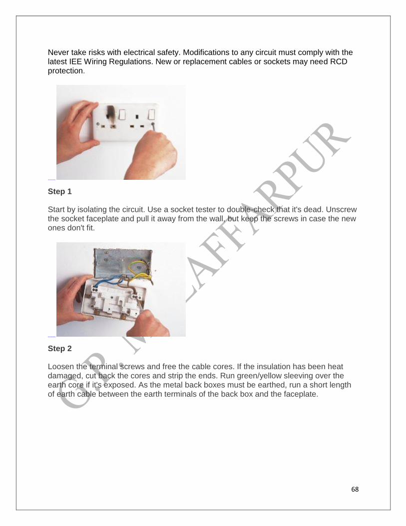
68
Never take risks with electrical safety. Modifications to any circuit must comply with the latest IEE Wiring Regulations. New or replacement cables or sockets may need RCD protection.
Zoom: [i mage descripti on]
Step 1
Start by isolating the circuit. Use a socket tester to double-check that it's dead. Unscrew the socket faceplate and pull it away from the wall, but keep the screws in case the new ones don't fit.
Zoom: [i mage descripti on]
Step 2
Loosen the terminal screws and free the cable cores. If the insulation has been heat damaged, cut back the cores and strip the ends. Run green/yellow sleeving over the earth core if it's exposed. As the metal back boxes must be earthed, run a short length of earth cable between the earth terminals of the back box and the faceplate.

69
Zoom: [i mage descripti on]
Step 3
Connect the live core or cores to the live terminal (L) of the new faceplate, the neutral to the neutral terminal (N) and the earth to the earth terminal (E or (Earth symbol)). Fully tighten the terminal screws, and fit the new faceplate. If the new screws don't fit the lugs of the old box, just re-use the original screws. Finally, use the socket tester to check you've wired everything correctly.
Precaution:
Use electrical cords only if they are in good condition. Cords must not be cracked, frayed, or
have corroded prongs.
Do not use 3-to-2 prong adapters unless other grounding provisions have been made. Plug 3-
prong plugs into 3-prong outlets.
Use power strips that have circuit breakers or fuses. Do not link power strips in series.
Do not leave cables and cords unsecured and hanging in areas where they can pose a trip and
movement hazard. Place cords so that they are not subjected to mechanical stress or
temperatures that could damage the insulation.
Do not conceal cords behind or attach electrical cords to building surfaces.
Do not leave electrical circuits exposed. Use electrical tape to insulate wires or use a guard as
cover to prevent accidental contact.
Do not block access to electrical panels.
Do not install standard electrical equipment in locations where flammable gases, vapors,
dusts, or other easily ignitable materials are present. If electrical equipment is used in a
chemical fume hood, elevate it to allow efficient air flow.
Related Documents