IP1000A LF Preliminary Data Sheet 1/75 July 5, 2005 Copyright © 2005, IC Plus Corp. IP1000A LF-DS-R08 Gigabit Ethernet NIC Single Chip Features z PCI & DMA Features – PCI Specification Revision 2.3 compliant – 32-bit, 33/66MHz bus master capability – Efficient DMA operation maximizes PCI band-width utilization – 1 Terabyte (40 bit) address space – Scatter, gather transmit/receive DMA – Transmit "interrupt-less" mode of operation – Receive frame priority interrupts – Receive interrupt coalescing z FIFO Features – No external memory required – Receive FIFO flow control thresholds – Configurable TX/RX FIFO z MAC Features – IEEE 802.3z, 802.3x compliant – IEEE 802.1p, 802.1Q compliant – 1000Mbps, 100Mbps, 10Mbps triple speed, half/full duplex operation – Transmit and receive back to back frames at full wire speed – Half duplex carrier extension and packet bursting – Asymmetric/symmetric flow control – VLAN tag insertion/removal – VLAN tagged frame filtering – IPV4/6, TCP, UDP checksum calculation/ verification – 802.3 MIB statistic register sets – 64-bit hash table for multicast frame filtering – Jumbo frame support for transmit/receive – Big-endian z Phsical Layer Features – Fully integrated IEEE 802.3ab compliant 1000BASE-T, 100BASE-TX and 10BASE-T port – DSP receiver includes feed-forward equalizer, decision feedback equalizer, echo canceller, crosstalk canceller, and baseline wander correction – 802.3ab compliant Auto-Negotiation for automatic speed, duplex, and master/slave configuration – Automatic MDI/MDI-X crossover function and polarity correction – Automatic pair skew adjustment – PHY management registers – Smart Cable Analyzer (SCA™) – Smart speed downshift – APS(Auto Power Saving) a. Power Saving with Link status detecting b. Keep only MAC alive through software setting z Power Management, EEPROM and Package – WakeOnLAN support – ACPI Revision 1.0 compliant – 1.8/3.3V CMOS with 5V tolerant I/O – EEPROM 93C46 support – Optional boot from serial ROM support – 128-pin LQFP with e-PAD package z Support Lead Free package (Please refer to the Order Information) General Description The IP1000A LF is a truly 10/100/1000Mbps Gigabit Ethernet NIC single chip which it incorporates a 32-bit PCI interface with bus master support. It is manufactured using standard digital CMOS process and contains all the active circuitry required to implement the physical layer functions to transmit and receive data on standard CAT5 unshielded twisted pair cable. The IP1000A LF is designed for use in a variety of applications including workstation NICs, and other systems utilizing a PCI bus. The IP1000A LF includes a 32-bit PCI bus interface, IEEE 802.3 compliant MAC, transmit and receive FIFO buffers, IEEE 802.3 compliant 10BASE-T, and 100BASE-TX PHY, IEEE 802.3z compliant 1000 BASE-T PHY, serial EEPROM interface, expansion ROM interface and LED drivers. The IP1000A LF supports features for use in “Green PCs” or systems where control over system power consumption is desired. The IP1000A LF supports several power down states, and the ability to issue a system “wake event” via reception of unique, user defined Ethernet frames. In addition, the IP1000A LF can assert a wake event in response to changes in the Ethernet link status. 查询IP1000ALF-DS-R08供应商 捷多邦,专业PCB打样工厂,24小时加急出货

Welcome message from author
This document is posted to help you gain knowledge. Please leave a comment to let me know what you think about it! Share it to your friends and learn new things together.
Transcript

IP1000A LF Preliminary Data Sheet
1/75 July 5, 2005Copyright © 2005, IC Plus Corp. IP1000A LF-DS-R08
Gigabit Ethernet NIC Single Chip Features
PCI & DMA Features – PCI Specification Revision 2.3 compliant – 32-bit, 33/66MHz bus master capability – Efficient DMA operation maximizes PCI
band-width utilization – 1 Terabyte (40 bit) address space – Scatter, gather transmit/receive DMA – Transmit "interrupt-less" mode of
operation – Receive frame priority interrupts – Receive interrupt coalescing
FIFO Features – No external memory required – Receive FIFO flow control thresholds – Configurable TX/RX FIFO
MAC Features – IEEE 802.3z, 802.3x compliant – IEEE 802.1p, 802.1Q compliant – 1000Mbps, 100Mbps, 10Mbps triple
speed, half/full duplex operation – Transmit and receive back to back frames
at full wire speed – Half duplex carrier extension and packet
bursting – Asymmetric/symmetric flow control – VLAN tag insertion/removal – VLAN tagged frame filtering – IPV4/6, TCP, UDP checksum calculation/
verification – 802.3 MIB statistic register sets – 64-bit hash table for multicast frame
filtering – Jumbo frame support for transmit/receive – Big-endian
Phsical Layer Features – Fully integrated IEEE 802.3ab compliant
1000BASE-T, 100BASE-TX and 10BASE-T port
– DSP receiver includes feed-forward equalizer, decision feedback equalizer, echo canceller, crosstalk canceller, and baseline wander correction
– 802.3ab compliant Auto-Negotiation for automatic speed, duplex, and master/slave configuration
– Automatic MDI/MDI-X crossover function and polarity correction
– Automatic pair skew adjustment – PHY management registers – Smart Cable Analyzer (SCA™) – Smart speed downshift – APS(Auto Power Saving)
a. Power Saving with Link status detecting b. Keep only MAC alive through
software setting
Power Management, EEPROM and Package – WakeOnLAN support – ACPI Revision 1.0 compliant – 1.8/3.3V CMOS with 5V tolerant I/O – EEPROM 93C46 support – Optional boot from serial ROM support – 128-pin LQFP with e-PAD package
Support Lead Free package (Please refer to
the Order Information) General Description
The IP1000A LF is a truly 10/100/1000Mbps Gigabit Ethernet NIC single chip which it incorporates a 32-bit PCI interface with bus master support. It is manufactured using standard digital CMOS process and contains all the active circuitry required to implement the physical layer functions to transmit and receive data on standard CAT5 unshielded twisted pair cable. The IP1000A LF is designed for use in a variety of applications including workstation NICs, and other systems utilizing a PCI bus. The IP1000A LF includes a 32-bit PCI bus interface, IEEE 802.3 compliant MAC, transmit and receive FIFO buffers, IEEE 802.3 compliant 10BASE-T, and 100BASE-TX PHY, IEEE 802.3z compliant 1000 BASE-T PHY, serial EEPROM interface, expansion ROM interface and LED drivers. The IP1000A LF supports features for use in “Green PCs” or systems where control over system power consumption is desired. The IP1000A LF supports several power down states, and the ability to issue a system “wake event” via reception of unique, user defined Ethernet frames. In addition, the IP1000A LF can assert a wake event in response to changes in the Ethernet link status.
查询IP1000ALF-DS-R08供应商 捷多邦,专业PCB打样工厂,24小时加急出货

IP1000A LF Preliminary Data Sheet
Block Diagram
PCI Bus
Interface
Physical
Layer
(PCS, PMA, PMD)
RX DMADual
QueueController
IP/TCP/UDPChecksumGeneration
TransmitFlow
Control
ReceiveFlow
Control
Media
Access
Control
(MAC)IP/TCP/UDPChecksumVerification
RXFIFO
TXFIFO
32 bitBus
Master
TX DMADual
QueueController
PCI
RSTN
PCICLK
GNTN
IDSEL
INTAN
REQN
AD[31:0]CBEN[3:0]
PAR
IRDYN
FRAMENTRDYN
DEVSELNSTOPN
PERRNSERRN
VDET
ANALOG MISC
MDI
EEPROM
EXPANSION ROM
LEDLED_LINK10NLED_LINK100NLED_LINK1000NLED_DUPLEXN
TP_MDI[3:0]+TP_MDI[3:0]-
LED_RXNLED_TXN
EESKEEDIEEDO
X2X1
RSETCTRL_REGA
MAIN CLOCK
PMEN
POWER AND GROUND
VSS1VSS2VCC1VCC2AVSSAVCC
AVCCH
EECS
BECSEESK
BootRom_HOLDBootRom_WEN
CTRL_REGD
EEDIEEDO
2/75 July 5, 2005Copyright © 2005, IC Plus Corp. IP1000A LF-DS-R08
IP1000A LF Preliminary Data Sheet
3/75 July 5, 2005Copyright © 2005, IC Plus Corp. IP1000A LF-DS-R08
Table Of Contents
Features..................................................................................................................................................................................1 General Description...............................................................................................................................................................1 Block Diagram .......................................................................................................................................................................2 Table Of Contents..................................................................................................................................................................3 Revision History.....................................................................................................................................................................4 PIN Diagram ..........................................................................................................................................................................5 1 PIN Description .............................................................................................................................................................6 PIN Description (continued) .................................................................................................................................................7 PIN Description (continued) .................................................................................................................................................8 PIN Description (continued) .................................................................................................................................................9 2 Function Description...................................................................................................................................................10
2.1 Physical Layer...................................................................................................................... 10 2.1.1 Introduction ............................................................................................................. 10 2.1.2 Receiver Fucntion ................................................................................................... 10 2.1.3 Transmit Function ....................................................................................................11 2.1.4 Link Function............................................................................................................11 2.1.5 Smart Cable Analyzer (SCA™)............................................................................... 12 2.1.6 Smart Speed Downshift .......................................................................................... 12
2.2 PCI ....................................................................................................................................... 12 2.2.1 Reset ……………………………………………………………………………………...13 2.2.2 FIFOs ……………………………………………………………………………………...13 2.2.3 DMA ……………………………………………………………………………………...13 2.2.4 Interrupts ................................................................................................................. 14 2.2.5 ACPI ……………………………………………………………………………………...15 2.2.6 Wake On LAN ......................................................................................................... 16
2.3 Media Access Control .......................................................................................................... 19 2.3.1 VLAN ……………………………………………………………………………………...20 2.3.2 Layer 3/4 Checksums ............................................................................................. 20 2.3.3 Flow Control ............................................................................................................ 21
3 Register Description ...................................................................................................................................................22 3.1 PHY Registers...................................................................................................................... 22
3.1.1 Control Register (Reg0) .......................................................................................... 23 3.1.2 Status Register (Reg1)............................................................................................ 24 3.1.3 PHY Identifier Register (Reg2) ............................................................................... 25 3.1.4 PHY Identifier Register (Reg3) ............................................................................... 25 3.1.5 Advertisement Register (Reg4) .............................................................................. 25 3.1.6 Link Partner Ability Register (Base Page) (Reg5) .................................................. 26 3.1.7 Auto-Negotiation Expansion Register (Reg6)......................................................... 26 3.1.8 Auto-Negotiation Next Page Transmit Register (Reg7).......................................... 27 3.1.9 Auto-Negotiation Link Partner Next Page Register (Reg8) .................................... 27 3.1.10 1000BASE-T Control Register (Reg9).................................................................... 28 3.1.11 1000BASE-T Status Register (Reg10) ................................................................... 28 3.1.12 Extended Status Register (Reg15) ......................................................................... 29
3.2 MAC Registers..................................................................................................................... 30 3.2.1 Ethernet MIB Statistics............................................................................................ 30 3.2.2 PCI Configuration Space Registers ........................................................................ 47 3.2.3 EEPROM Fields...................................................................................................... 61
4 Absolute Maximum Ratings.......................................................................................................................................66 5 Operating Ranges.......................................................................................................................................................66 6 DC Characteristics......................................................................................................................................................66 7 Switching Characteristics...........................................................................................................................................68 8 Order Information........................................................................................................................................................74 9 Package Detail ............................................................................................................................................................75

IP1000A LF Preliminary Data Sheet
4/75 July 5, 2005Copyright © 2005, IC Plus Corp. IP1000A LF-DS-R08
Revision History
Revision # Change Description IP1000A LF-DS-R01 1. Initial release. IP1000A LF-DS-R02 1. Adding package information, 128-pin LQFP with e-PAD, in page-1 and page-67
order information. IP1000A LF-DS-R03 1. Modify I/O Register in page-4 and page-49
2. Modify Wake Signal in page-17, page-20 and page-60 3. Modify DeviceId in page-54 4. Modify Default setting as 0 in page-64
IP1000A LF-DS-R04 1. Add EXP-ROM Disable Bit in EEPROM content, in page64 2. Add EEPROM Disable Bit in EEPROM content, in page64 3. Add POA Disable Bit in EEPROM content, in page65 4. Add LED Mode, flashing speed and DSP setting parameter in EEPROM content,
in page68 IP1000A LF-DS-R05 1. Add DC characteristic, in page69
2. Add EXP-ROM Timing diagram, in page71,72, 74, 75 3. Pin48 modify as “Left Floating”, in page 7 4. RevisionID = 41, in page62 5. Delete POA description, in page1, 65 6. Modify jumbo description, in page1 7. Swap Pin31, Pin32 type Input and output, in page 8
IP1000A LF-DS-R06 1. Add detailed power consumption for for different voltage, in page 68 2. Remove IntRequested and countdown description, in page 15. 3. Remove receive interrupt coalescing description, in page 16. 4. Remove TCP segmenation, in page 23. 5. Modify VendorID description, in page62 6. Modify Minimum Core Voltage from 1.71V to 1.73V, in page68, 69
IP1000A LF-DS-R07 1. Add the order information for lead free package. IP1000A LF-DS-R08 1. Remove description about 93C56, support 93C46 only, in page-1, 6

IP1000A LF Preliminary Data Sheet
PIN Diagram 1 2 9876543 10 11 383736353433323130292827262524232221201918171615141312
3940414243444546474849505152535455565758596061626364
656667686970717273747576777879808182838485868788899091929394959697989910 010 110 2
103104105106107108109110111112113114115116117118119120121122123124125126127128
VC
C1
AD5
AD4
AD3
VSS
2AD
2AD
1C
TRL_
RE
GD
AD0
VC
C1
VC
C2
VSS
1V
SS2
LED
_LIN
K10
00N
(EE
_OP
)V
CC
1LE
D_T
XN
LED
_LIN
K10
N
(EE
SK)
LED
_LIN
K100
N (E
ED
I)V
SS1
VC
C2
LED
_RX
NLE
D_D
UP
LEX
N (E
ED
O)
VS
S2V
CC
1TE
ST
VC
C2
BEC
SE
ECS
VC
C2
NC X2
X1
VSS
2R
SET
AVS
STP
_MD
I0 +
TP_M
DI0
-A
VSS
TRD
YN
IRD
YNFR
AMEN
VCC
2VC
C1
VSS
2C
BE2
NAD
16VS
S1
AD17
VCC
1VC
C2
AD18
VSS
2AD
19VS
S1
AD20
AD21
AD22
AD23
IDS
ELVC
C1
CB
E3N
AD24
VSS
1AD
25AD
26VS
S2
VCC
2AD
27AD
28AD
29AD
30AD
31R
EQ
NPC
ICLK
VCC
2VS
S2
VSS1PMENGNTNRSTNVDETINTANAVCCAVSSTP_MDI3 -TP_MDI3 +AVSSAVCCAVSSTP_MDI2 -TP_MDI2 +AVSSHSDAC_PAVCCHAVSSCTRL_REGAAVCCAVSSTP_MDI1 -TP_MDI1 +AVSSAVCCVSS1
AD6AD7
CBE0NAD8AD9
VSS2VCC2VCC1VSS1AD10AD11AD12AD13AD14AD15
CBE1NVCC2VSS1VSS2PAR
SERRNVCC1
PERRNSTOPN
DEVSELN
IP1000A LF
5/75 July 5, 2005Copyright © 2005, IC Plus Corp. IP1000A LF-DS-R08
IP1000A LF Preliminary Data Sheet
6/75 July 5, 2005Copyright © 2005, IC Plus Corp. IP1000A LF-DS-R08
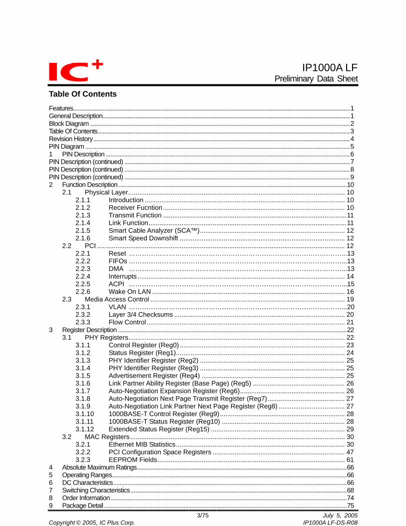
1 PIN Description
Pin no. Label Type Description Medium Interface 36, 37, 41, 42, 50, 51, 55, 56
TP_MDI [3:0]+/- I/O Twisted- Pair Media Dependent Interface [3:0] In 1000BASE-T mode, all 4 pairs are both input and output at the same time. In 100BASE-TX and 10BASE-T mode, one pair of TP_MDI [1:0]+/- is used for transmit pair and the other is used for receive pair. TP_MDI [3:2]+/- are unused in 100BASE-TX and 10BASE-T mode.
Analog misc 48 HSDAC_P O Test Pin
Left floating 8 CTRL_REGD O Digital Regulator Control.
Regulator control to generate 1.8V supply. 45 CTRL_REGA O Analog Regulator Control.
Regulator control to generate 1.8V supply. 34 RSET I Reference.
External 6.2 kΩresistor connection as bandgap resistor. LED 17 LED_LINK10N
EESK
O
O
LINK 10Mb/s LED. 10BASE-T Link Indicator. This pin is shared with EEPROM/serial ROM clock
18 LED_LINK100N EEDI
O
O
LINK 100Mb/s LED. 100Mb/s Link Indicator. This pin is shared with EEPROM/serial ROM Data Input
14 LED_LINK1000N O LI
LINK 1000Mb/s LED.
22 LED_DUPLEXN EEDO
O I
Duplex LED. Duplex or Duplex/Collision indicator. This pin is shared with the output from EEPROM/serial ROM
21 LED_RXN BootRom_HOLD
O Receive LED. Receive Activity. shared pin of output to serial Rom for HOLD
16 LED_TXN BootRom_WEN
O Transmit LED. Transmit Activity. shared pin of output to serial Rom for write enable(active low)
IP1000A LF Preliminary Data Sheet
7/75 July 5, 2005Copyright © 2005, IC Plus Corp. IP1000A LF-DS-R08
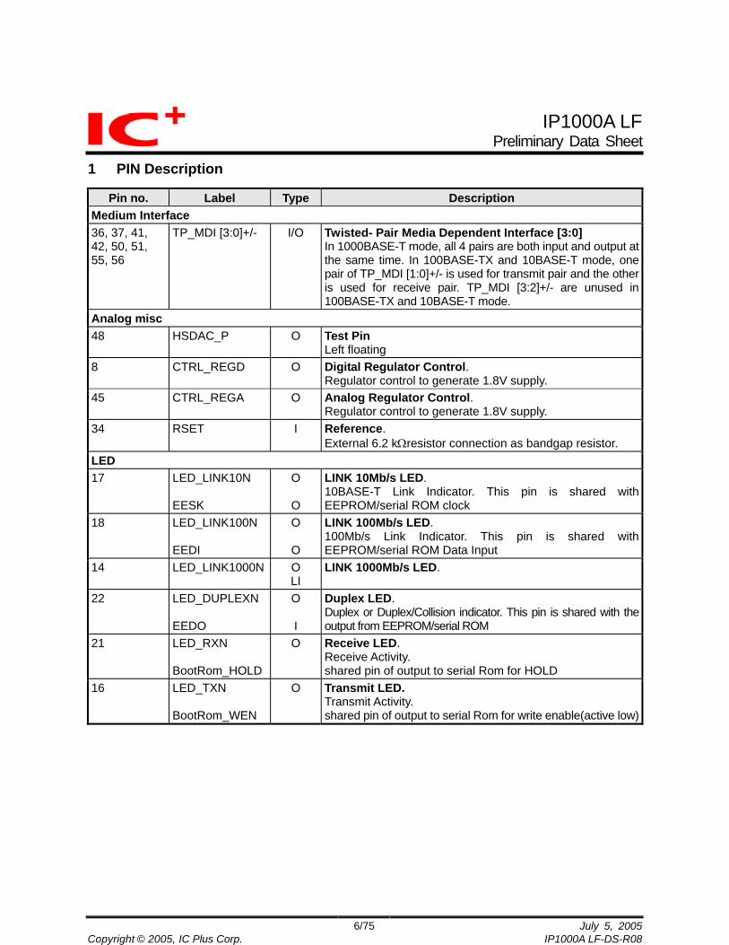
PIN Description (continued)
Pin no. Label Type Description Main Clock 31 X2 O Reference Clock.
25 MHz crystal reference. 32 X1 I Reference Clock.
25 MHz crystal reference or oscillator input. PCI interface 60 VDET I Power Detect.
The IP1000A LF detects whether PCI bus power supply is available or not from this pin.
59 INTAN O Interrupt Request, asserted LOW. The IP1000A LF asserts INTAN to request an interrupt, when any one of the programmed interrupt event occurs.
61 RSTN I Reset, asserted LOW. RSTN will cause the IP1000A LF to reset all of its functionalblocks. RSTN must be asserted for a minimum duration of 10 PCICLK cycles. While RSTN is asserted, the IP1000A LF PCI interface is placed in an isolated state. When the IP1000A LF PCI bus is isolated, all PCI output and bi-directional signals are placed in a high impedance state, and all inputs are ignored. The IP1000A LF will remain in a reset state for approximately 380ns following the de-assertion of RSTN.
63 PMEN O Wake Event, assertion level is programmable. The IP1000A LF asserts PMEN to signal the detection of a wake event. The PMEN signal eventually drives the PCI bus PME# signal, but not intended to be directly connected to PME#. See the PCI Bus Power Management InterfaceSpecification for details on generating PME# from PMEN.
108 PAR I/O Parity. PCI Bus parity is even across bits 0 through 31 of AD and bits 0 through 3 of CBEN. The IP1000A LF generates PAR during address and write data phases as a bus master, and during read data phase as a target. It checks for correct parity during read data phase as bus master, during every address phase as a bus slave, and during write data phasesas a target.
100 FRAMEN I/O PCI Bus Cycle Frame, asserted LOW. FRAMEN is asserted at the beginning of the address phase of the bus transaction and de-asserted before the final transfer of the data phase of the transaction.
102 TRDYN I/O Target Ready, asserted LOW. A bus target asserts TRDYN to indicate valid read data phases, and to indicate it is ready to accept data duringwrite data phases. A bus master will monitor TRDYN.

IP1000A LF Preliminary Data Sheet
8/75 July 5, 2005Copyright © 2005, IC Plus Corp. IP1000A LF-DS-R08
PIN Description (continued)
Pin no. Label Type Description PCI interface (continued) 101 IRDYN I/O Initiator Ready, asserted LOW.
A bus master asserts IRDYN to indicate valid data phases on AD during write data phases, and to indicate it is ready to accept data during read data phases. A target will monitorIRDYN.
104 STOPN I/O Stop, asserted LOW. STOPN is driven by the slave target to inform the bus master to terminate the current transaction.
103 DEVSELN I/O Device Select, asserted LOW. The IP1000A LF asserts DEVSELN when it is selected as a target during a bus transaction. It monitors DEVSELN forany target to acknowledge a bus transaction initiated by the IP1000A LF.
82 IDSEL I Initialization Device Select. The IDSEL is used to select the IP1000A LF duringconfiguration read and write transactions.
67 PCICLK I PCI Bus Clock. This clock is used to drive the PCI bus interfaces and the internal DMA logic. All bus signals are sampled on the rising edge of PCICLK. PCICLK can operate from 0MHz to 66MHz, on a PCI bus.
105 PERRN I/O Parity Error, asserted LOW. The IP1000A LF asserts PERRN when it checks and detects a bus parity error. When it is generating PAR output, the IP1000A LF monitors for any reported parity error on PERRN.
107 SERRN O System Error, asserted LOW. 68 REQN O Request, asserted LOW.
The IP1000A LF asserts REQN to request PCI bus master operation.
62 GNTN I PCI Bus Grant, asserted LOW. GNTN signals access to the PCI bus has been granted to IP1000A LF.
80, 96, 112, 125
CBE [3:0] N I/O PCI Bus Command/Byte Enable, asserted LOW. Bus command and byte enables are multiplexed on the CBEN signals. CBEN specify the bus command during the address phase transaction, and carry byte enables during the data phase.

IP1000A LF Preliminary Data Sheet
9/75 July 5, 2005Copyright © 2005, IC Plus Corp. IP1000A LF-DS-R08
PIN Description (continued)
Pin no. Label Type Description PCI address/data bus 2, 3, 4, 6, 7, 9, 69, 70, 71, 72, 73, 76, 77, 79, 83, 84, 85, 86, 88, 90, 93. 95, 113, 114, 115, 116, 117, 118, 123, 124, 126, 127,
AD [31:0] I/O PCI Bus Address/Data. Address and data are multiplexed on the AD pins. Bits 0 through 31 carry the lower 32 bits of the physical address during the first clock cycle of a transaction, and carry data during the subsequent clock cycles.
EEPROM interface / EXPANSION ROM 27 BECS
O Boot ROM Chip Select
Note: EESK, EEDI, EEDO are shared with EEPROM 28 EECS O EEPROM Chip Select Test pins 25 TEST I,PU Selection of internal test ( tied to ground for normal mode )30 NC I,PU NC Analog Power and Ground 47 AVCCH Power Analog Power 3.3V 39, 44, 53, 58 AVCC Power Analog Power 1.8V. 35, 38, 40, 43, 46, 49, 52, 54, 57
AVSS Ground Analog Ground
Digital Power and Ground 11, 20, 26, 29, 66, 74, 91, 99, 111, 121
VCC2 Power Digital I/O Power 3.3V
1, 10, 15, 24, 81, 92, 98, 106, 120
VCC1 Power Digital Core Power 1.8V.
5, 13, 23, 33, 65, 75, 89, 97, 109, 122
VSS2 Ground Digital Ground
8, 12, 19, 64, 78, 87, 94, 110, 119, 128
VSS1 Ground Digital Ground
IP1000A LF Preliminary Data Sheet
2 Function Description
2.1 Physical Layer 2.1.1 Introduction
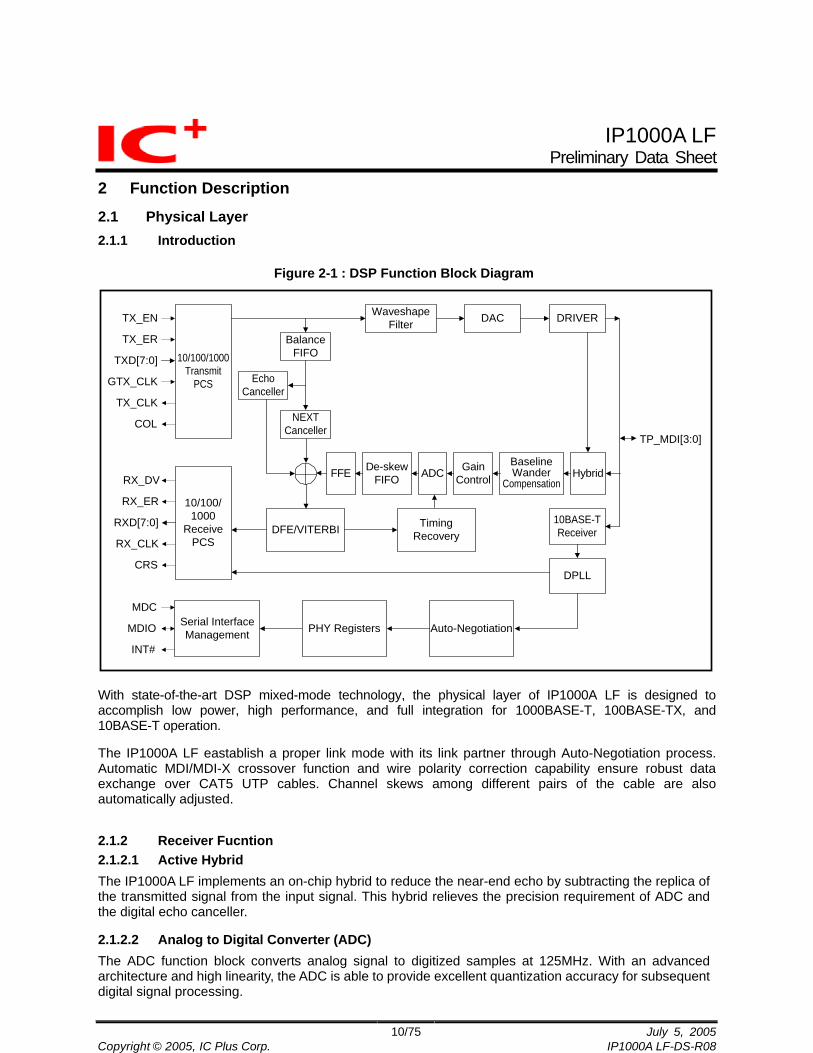
Figure 2-1 : DSP Function Block Diagram
10/100/1000Transmit
PCS
TX_EN
TXD[7:0]
TX_ER
COL
TX_CLK
GTX_CLK
10/100/1000
ReceivePCS
CRS
RX_CLK
RXD[7:0]
RX_ER
RX_DV
BalanceFIFO
NEXTCanceller
EchoCanceller
HybridBaselineWander
CompensationGain
ControlADCDe-skewFIFOFFE
DFE/VITERBI
WaveshapeFilter DAC DRIVER
TimingRecovery
10BASE-TReceiver
DPLL
Auto-NegotiationSerial InterfaceManagement PHY Registers
MDC
MDIO
INT#
TP_MDI[3:0]
With state-of-the-art DSP mixed-mode technology, the physical layer of IP1000A LF is designed to accomplish low power, high performance, and full integration for 1000BASE-T, 100BASE-TX, and 10BASE-T operation. The IP1000A LF eastablish a proper link mode with its link partner through Auto-Negotiation process. Automatic MDI/MDI-X crossover function and wire polarity correction capability ensure robust data exchange over CAT5 UTP cables. Channel skews among different pairs of the cable are also automatically adjusted. 2.1.2 Receiver Fucntion 2.1.2.1 Active Hybrid The IP1000A LF implements an on-chip hybrid to reduce the near-end echo by subtracting the replica of the transmitted signal from the input signal. This hybrid relieves the precision requirement of ADC and the digital echo canceller. 2.1.2.2 Analog to Digital Converter (ADC) The ADC function block converts analog signal to digitized samples at 125MHz. With an advanced architecture and high linearity, the ADC is able to provide excellent quantization accuracy for subsequent digital signal processing.
10/75 July 5, 2005Copyright © 2005, IC Plus Corp. IP1000A LF-DS-R08

IP1000A LF Preliminary Data Sheet
11/75 July 5, 2005Copyright © 2005, IC Plus Corp. IP1000A LF-DS-R08
2.1.2.3 Echo Canceller With the proprietary architecture, the adaptive digital echo canceller further reduces the residual echo not removed by the hybrid, the reflection due to patch cord impedance mismatch and non-ideal cable characteristics. 2.1.2.4 NEXT Canceller When IP1000A LF is operated in 1000BASE-T mode, it uses 4 pairs of wires to transmit and receive data at the same time. This results in a detrimental near-end crosstalk between adjacent pairs and significantly impairs the receiver performance. An adaptive digital NEXT canceller is implemented in IP1000A LF to mitigate this effect. 2.1.2.5 Baseline Wander Canceller IP1000A LF implements a digital adaptive baseline wander cancellation circuit to compensate DC shifts, which are result of the DC loss from the transformer. 2.1.2.6 Feed-Forward Equalizer (FFE) and Decision-Feedback Equalizer (DFE) The FFE and DFE of IP1000A LF are designed to remove inter-symbol interference. These fully adaptive filters can track the inherently time-variant channel environment. 2.1.2.7 Digital Timing Recovery IP1000A LF adopts a digital timing recovery scheme to accurately acquire the timing information at the receiver side. This advanced digital timing recovery block reduces both long-term and short-term frequency jitter to achieve as low bit error rate as possible. The maximum frequency offset it can track far exceeds the requirement of the IEEE standard. 2.1.2.8 Decoder The IP1000A LF implements different decoders for 1000BASE-T, 100BASE-TX, and 10BASE-T respectively. 2.1.3 Transmit Function 2.1.3.1 Digital to Analog Converter (DAC) The IP1000A LF incorporates a hightly integrated DAC to transmit Normal Link Pulse (NLP), Fast Link Pulse (FLP), Manchester coded symbols, MLT3 waveform, or partial response PAM5 signals. 2.1.3.2 Encoder The IP1000A LF implements different encoders for 1000BASE-T, 100BASE-TX, and 10BASE-T respectively. 2.1.4 Link Function 2.1.4.1 Medium Dependent Interface (MDI) The IP1000A LF transmits and receives data with all four pairs of wires in 1000BASE-T mode. If the IP1000A LF is operated in 100BASE-TX or 10BASE-T mode, only one pair is responsible for transmitting and the other for receiving data. 2.1.4.2 Automatic MDI/MDI-X Crossover and Pair Polarity Correction The IP1000A LF is able to correct pair polarity errors in all modes. The automatic crossover function will adjust MDI/MDI-X crossover condition for proper operation. In addition, the IP1000A LF can also correct two types of abnormal cable configuration not compliant with the IEEE 802.3ab standard. This function can be turned off by setting PHY register 20.2 to “0”.

IP1000A LF Preliminary Data Sheet
12/75 July 5, 2005Copyright © 2005, IC Plus Corp. IP1000A LF-DS-R08
Table Assignment of PMA signal to MDI and MDI-X pin-outs
RJ-45 Contact IP1000A LF pins
MDI MDI-X Abnormal type 1 Abnormal type 2
1 TP_MDI[0]+ BI_DA+ BI_DB+ BI_DA+ BI_DB+ 2 TP_MDI[0]- BI_DA - BI_DB - BI_DA - BI_DB - 3 TP_MDI[1]+ BI_DB+ BI_DA+ BI_DB+ BI_DA+ 6 TP_MDI[1]- BI_DB - BI_DA - BI_DB - BI_DA - 4 TP_MDI[2]+ BI_DC + BI_DD+ BI_DD+ BI_DC + 5 TP_MDI[2]- BI_DC - BI_DD - BI_DD - BI_DC - 7 TP_MDI[3]+ BI_DD+ BI_DC+ BI_DC+ BI_DD+ 8 TP_MDI[3]- BI_DD - BI_DC - BI_DC - BI_DD -
2.1.4.3 Auto-Negotiation and Next Page Exchange When the IP1000A LF is not set in forced mode, Auto-Negotiation automatically configures IP1000A LF for 1000BASE-T/100BASE-TX/10BASE-T, full/half duplex, and master/slave operation based on the highest common factor of both link capabality. IP1000A LF is able to perform next page exchanges. This function can be turned on/off manually by changing the register setting (PHY register 4.15). The content of the next page is based on PHY registers 7 and 8, respectively. When IP1000A LF is operated in 1000BASE-T, the next page exchanges are automatically turned on. 2.1.5 Smart Cable Analyzer (SCA™) To simplify the Gigabit link establishment, the IP1000A LF incorporates the “Smart Cable Analyzer” (SCA™) feature . This feature helps to make cable diagnosis an easy task for end users. If there is an improperly installed cable, the signal quality can be severly deteriorated to prevent from achieving a high SNR, which as result this leads to a poor networking performance. Furthermore, if the cable is open-circuited or short-circuited in any pair of wires, a Gigabit link is impossible. SCA can detect opens, shorts or impedance mismatch of a cable. It can also pinpoint the distance of the problematic segment to enable a quick troubleshooting. 2.1.6 Smart Speed Downshift A normal CAT5 cable has four pairs of wires. However, there exist some legacy cables with only two pairs of wires sufficient for a successful 100Mbps or 10Mbps operation. With the such cables, two Gigabit devices can agree on 1000Mbps speed via Auto-Negotiation but will never set up a successful link. The IP1000A LF can detect this “hangup” condition and downshifts to 100Mbps speed after several repeated failed tries in 1000 Mbps mode. The default downshift feature is turned on. It can be turned off by setting PHY register 16.11 to “0”. 2.2 PCI The PCI Bus Interface (PBI) implements the procedures and algorithms needed to link the IP1000A LF to a PCI bus. The IP1000A LF can be either a PCI bus master or slave. The PBI is also responsible for managing the DMA interfaces and the host processor accessing to the IP1000A LF registers. The PBI also manages interrupt generation for a host processor.

IP1000A LF Preliminary Data Sheet
13/75 July 5, 2005Copyright © 2005, IC Plus Corp. IP1000A LF-DS-R08
The IP1000A LF supports all of the PCI memory commands and decides on a burst-by-burst basis to issue which command to use in order to maximize bus efficiency. The list of PCI memory commands used by the IP1000A LF is shown below. For all commands, read and write commands are with respect to the IP1000A LF (i.e. read implies the IP1000A LF obtains information from an off-chip location, write implies the IP1000A LF sends information to an offchip location). Memory Read (MR) Memory Read Line (MRL) Memory Read Multiple (MRM) Memory Write (MW) Memory Write Invalidate (MWI) MR is used for all fetches of descriptor information. For reads of transmit frame data, MR, MRL, or MRM is used, depending upon the remaining number of bytes in the fragment, the amount of free space in the Transmit FIFO, and whether the Receive DMA Logic is requesting a bus master operation. MW is used for all descriptor writes. Writes of receive frame data use either MW or MWI, depending upon the remaining number of bytes in the fragment, the amount of frame data in the Receive FIFO, and whether the Transmit DMA Logic is requesting a bus master operation. The IP1000A LF provides two configuration bits to control the use of advanced memory commands. The MwlEnable bit in the ConfigCommand register allows the host to enable or disable the use of MWI. The MWIDisable bit in the DMACtrl register allows the host system the ability to disable the use of MWI PCI command. The IP1000A LF provides a set of registers that control the PCI burst behavior. These registers allow a trade-off to be made between PCI bus efficiency and underrun/overrun frequency. In support of bus isolation requirements for system states in which the IP1000A LF is powered down, all IP1000A LF PCI outputs will enter the tri-state condition when the RSTN is active. 2.2.1 Reset When the host system issues a reset to the IP1000A LF via the AsicCtrl register, a delay of at least 5ms is required before any register access should be attempted. 2.2.2 FIFOs The IP1000A LF uses a single configurable 32KB single-port SRAM for both the transmit and receive FIFOs. 2.2.3 DMA The IP1000A LF implements scatter gather Direct Memory Access (DMA) for moving data from the IP1000A LF to/from the host’s system memory. Two independent DMA processes are used to transfer transmit data from host system memory to the IP1000A LF (transmit DMA), and to transfer receive data from the IP1000A LF to host system memory (receive DMA). 2.2.3.1 Transmit DMA To utilize the IP1000A LF to transmit data onto a Gigabit Ethernet network, the data to be transmitted must be transferred from the host’s system memory to the IP1000A LF. The data bus utilized by the IP1000A LF for this data transfer is the PCI bus, and the method for transferring the data is DMA. The locations within system memory which contain the data to be transmitted are indicated to the IP1000A LF using Transmit Frame Descriptors.
IP1000A LF Preliminary Data Sheet
14/75 July 5, 2005Copyright © 2005, IC Plus Corp. IP1000A LF-DS-R08
The Transmit Frame Descriptor (TFD) is a data structure containing fields specifying a pointer to another TFD (the TFDNextPtr field), control information (the TFC0 field), and from one to 15 pointers to locations within system memory containing the Ethernet frame data (the FragInfo fields). The TFD is used to indicate to the IP1000A LF which blocks of system memory comprise the Ethernet frame data to be transmitted. Each Ethernet frame is described by one and only one TFD. 2.2.3.2 Receive DMA To utilize the IP1000A LF to receive data from a Gigabit Ethernet network, the received data must be transferred from the IP1000A LF to the host’s system memory. The data bus utilized by IP1000A LF for this data transfer is the PCI bus, and the method for transferring the data is DMA. The locations within system memory reserved for the received data are indicated to IP1000A LF using Receive Frame Descriptors. The Receive Frame Descriptor (RFD) is a data structure containing fields specifying a pointer to another RFD (the RFDNextPtr field), status information (the RFS field), and one pointer (the FragInfo field) to a unique, contiguous block of system memory which is reserved for holding the received data. Typically, one RFD will completely specify a single received Ethernet frame. While it is possible to use multiple RFDs to describe a single Ethernet frame, it is not possible to describe multiple Ethernet frames with a single RFD. 2.2.4 Interrupts The IP1000A LF generates host system processor interrupts via the PCI bus based on events related to transmit and receive DMA operation. It is the responsibility of the host system to detect these interrupts, identify the corresponding condition which caused the interrupt, and take the appropriate action. At gigabit per second data rates, interrupts related to Gigabit Ethernet frame transmission and reception can quickly overwhelm a host system processor. The IP1000A LF incorporates several features for minimizing the number of interrupts generated. These features should be carefully understood and utilized to achieve maximum system performance in Gigabit Ethernet networks. 2.2.4.1 Transmit DMA Interrupts Interrupts can be generated by the IP1000A LF based on a number of events related to transmit DMA operation: TxDMAComplete interrupt is issued after successful transfer of an Ethernet frame to the IP1000A LF
via transmit DMA with the TxDMAIndicate bit in the TFD’s TFC0 field is a logic 1. Use of this interrupt is not recommended due to the frequency of transmit DMA operations in a Gigabit Ethernet network.
TxComplete interrupt (frame transmission complete without error) is issued after successful transmission of an Ethernet frame which has already been transferred to the IP1000A LF with the TxIndicate bit in the TFD’s TFC0 field is a logic 1. A recommended use of this feature is to avoid setting the TxIndicate bit in every TFD, but instead only set the TxIndicate bit in the last TFD of a TFDList, or in every Nth frame (where N>1).
TxComplete interrupt (frame transmission encountered an error) is issued if an error occurs during transmission of an Ethernet frame which has already been transferred to the IP1000A LF independent of the TxIndicate bit setting in the TFD’s TFC0 field. When an error occurs, the transmit MAC of the IP1000A LF is disabled (and must be re-enabled to resume operation). Transmit DMA operation continues in spite of transmit errors except for the case of a transmit underrun error (indicated by the TxUnderrun bit in the TxStatus register). To resume transmit DMA operation after a transmit underrun error, the transmit DMA, transmit FIFO, and transmit MAC functions within IP1000A LF must be reset.

IP1000A LF Preliminary Data Sheet
15/75 July 5, 2005Copyright © 2005, IC Plus Corp. IP1000A LF-DS-R08
A common use of interrupts during transmit DMA operation is to determine which TFDs have been successfully transmitted so the host system can free the memory occupied by old TFDs. Interrupts however usually incur a significant cost in terms of host system performance, requiring a large percentage of processor time to service. While interrupts are expensive, memory is usually abundant, therefore a trade off which minimizes interrupts in exchange for more memory usage is desirable. 2.2.4.2 Interrupt-Less Transmit DMA IP1000A LF's transmit DMA can operate without generating host system processor interrupts. In this mode of operation, the host system does not set the TxIndicate or TxDMAIndicate bits in the TFC0 field of any TFDs used to transfer Ethernet frames from system memory. Thus, an interrupt is not issued by the IP1000A LF to indicate successful DMA transfer or successful transmission of each Ethernet frame. An interrupt will only be issued by the IP1000A LF in the event of a transmit error, but this case should be rare. Without the use of interrupts, the IP1000A LF provides another mechanism for the host system to determine which Ethernet frames have been successfully transmitted. This mechanism allows the host system to free memory locations holding old TFD lists. This “interrupt-less” mechanism involves using the TxFrameId field of the TxStatus register. The TxFrameId field of the TxStatus register indicates the last Ethernet frame which was successfully transmitted. Using this information, the host system can infer successful transmission of all Ethernet frames up to the frame indicated by the TxFrameId field of the TxStatus register. Thus, the host system decides when to poll the TxFrameId field of the TxStatus register (for example, when the amount of memory occupied by old TFD lists becomes excessive) and avoid generation of processor intensive interrupts by the IP1000A LF. 2.2.4.3 Receive DMA Interrupts Interrupts can be generated by the IP1000A LF based on a number of events related to receive DMA operation: RxDMAComplete interrupt is issued after successful transfer of one or more Ethernet frames (based
on the interrupt coalescing configuration) from the IP1000A LF to the host system memory. Interrupt coalescing should be used in conjunction with the RxDMAComplete interrupt given the frequency of frame receipts in a Gigabit Ethernet network.
RxDMAPriority interrupt is issued if a received Ethernet frame contains a Tag Control Information field with priority greater than or equal to the priority set in the RxDMAIntCtrl register.
RFDListEnd interrupt is issued if the end of the RFD list is reached (indicated by an RFDNextPtr field with a value of 0x0000000000), or a RFD with the RFDDone bit of the RFS field with a value of logic 1 is encountered.
2.2.4.4 Receive DMA Interrupt Coalescing A common use of interrupts during receive DMA operation is to indicate when new Ethernet frames have been transferred to host system memory. Interrupts however usually incur a significant cost in terms of host system performance, requiring a large percentage of processor time to service. One way to minimize the number of interrupts issued by the IP1000A LF related to receive DMA operation is to issue a single interrupt to indicate multiple Ethernet frames have been received. While minimizing interrupts can improve host system performance, it can also require more host system memory usage, and increase network latency. Therefore, a balance between interrupt frequency and network latency must be reached by the host system to optimize performance. Note: interrupt coalescing only applies to the nominal TFD list. Priority TFD lists do not utilize interrupt coalescing. 2.2.5 ACPI The IP1000A LF supports operating system directed power management according to the ACPI specification. Power management registers in the PCI configuration space, as defined by the PCI Bus Power Management Interface specification, Revision 1.1

IP1000A LF Preliminary Data Sheet
16/75 July 5, 2005Copyright © 2005, IC Plus Corp. IP1000A LF-DS-R08
2.2.5.1 Power Management States The IP1000A LF supports several power management states. The PowerState field in the PowerMgmtCtrl register determines IP1000A LF’s current power state. The power states are defined as follows: D0 Uninitialized (power state 0) is entered as a result of hardware reset, or after a transition from D3
Hot to D0. This state is the same as D0 Active except that the PCI configuration registers are uninitialized. In this state, the IP1000A LF responds to PCI configuration cycles only.
D0 Active (power state 0) is the normal operational power state for the IP1000A LF. In this state, the PCI configuration registers have been initialized by the system, including the IoSpace, MemorySpace, and BusMaster bits in the ConfigCommand register, so the IP1000A LF is able to respond to PCI I/O, memory and configuration cycles and can operate as a PCI master. The IP1000A LF cannot signal wake (PMEN on the PCI bus) from the D0 state.
D1 (power state 1) is a “light-sleep” state. The IP1000A LF optionally supports this state determined by the D1Support bit in the ConfigParm word in the EEPROM. The D1 state allows transition back to D0 with no delay. In this state, the IP1000A LF responds to PCI configuration accesses, to allow the system to change the power state. The IP1000A LF’s function in the D1 state is to recognize wake events and link state events and pass them on to the system by asserting the PMEN signal on the PCI bus.
D2 (power state 2) is a partial power-down state. The IP1000A LF optionally supports this state determined by the D2Support bit in the ConfigParm word in the EEPROM. D2 allows a faster transition back to D0 than is possible from the D3 state. In this state, the IP1000A LF responds to PCI configuration accesses, to allow the system to change the power state. In D2 the IP1000A LF does not respond to any PCI I/O or memory accesses. The IP1000A LF’s function in the D2 state is to recognize wake events and link state events and pass them on to the system by asserting the PMEN signal on the PCI bus.
D3 Hot (power state 3) is the full power-down state for the IP1000A LF. In this state, the IP1000A LF responds to PCI configuration accesses, to allow the system to change the power state back to D0 Uninitialized. In D3 hot, the IP1000A LF does not respond to any PCI I/O or memory accesses. The IP1000A LF’s main responsibility in the D3 Hot state is to recognize wake events and link state events and signal those to the system by asserting the PMEN signal on the PCI bus.
D3 Cold (power state undefined) is the power-off state for the IP1000A LF. The IP1000A LF does not function in this state. When power is restored, the system guarantees the assertion of hardware reset, which puts the IP1000A LF into the D0 Uninitialized state.
2.2.6 Wake On LAN Wake on LAN is a key component of the IBM/Intel® Advanced Manageability Alliance (AMA) initiative. The IP1000A LF implements a portion of the Wake On LAN functionality defined by the AMA initiative. Specifically, the IP1000A LF can be configured to respond to wake up frames sent by a Wake On LAN managerment station. 2.2.6.1 Wake Events The IP1000A LF can generate wake events to the system as a result of Wake Packet reception, Magic Packet reception, or due to a change in the link status. The WakeEvent register gives the host system control over which of these events are passed to the system. Wake events are signaled over the PCI bus using the PMEN signal. A Wake Packet event is controlled by the WakePktEnable bit in WakeEvent register. The WakePktEnable bit has no effect when IP1000A LF is in the D0 power state, as the wake process can only take place in states D1, D2, or D3. When the IP1000A LF detects a Wake Packet, it signals a wake event on PMEN (if PMEN assertion is enabled), and sets the WakePktEvent bit in the WakeEvent register. The IP1000A LF can signal that a wake event has occurred when it receives a pre-defined frame from another station. The host system transfers a set of frame data patterns into the transmit FIFO using the TxDMA function before placing the IP1000A LF in a power-down state. Once powered down, the IP1000A LF compares

IP1000A LF Preliminary Data Sheet
receive frames with the frame patterns in the transmit FIFO. When a matching frame is received (and also passes the filtering mode set in the Receive-Mode register), a wake event is signaled. Frame patterns are written to the transmit FIFO in a single “pseudo-packet”. Prior to transferring this pseudo-packet, the host system should first set the TxReset in the AsicCtrl (to reset the transmit FIFO pointers and prevent transmission) then prepare a TFD that points to a single data buffer. The buffer should contain one or more frame patterns placed contiguously. The number of frame patterns is limited by the transmit FIFO size. The FragLen field in the TFD must exactly equal the sum of the frame pattern bytes. Also, the host system must set the WordAlign field to ‘x1’ in the TFC0 field of the TFD to prevent frame word-alignment. Finally, the host system must write the TFD’s address to the TFDListPtr register to transfer the frame into the transmit FIFO. The frame patterns in the transmit FIFO specify which bytes in received frames are to be examined. Each byte in the transmit FIFO specifies a four bit relative offset (from the start of the received frame) in the most significant nibble and a four bit length indicator in the least significant nibble. Relative offsets describe the number of bytes of the received frame to skip from the last relevant byte, beginning with byte 0x00. Relative offsets with a value of 0xF indicate the actual relative offset is larger than 15, and is specified by the next 8 bit value in the transmit FIFO. Length indicators with a value of 0xF indicate the actual length indicator is larger than 15, and is specified by the next 8 bit value in the transmit FIFO. If both the relative offset, and the length indicator are 0xF, the first byte following the relative offset/length indicator pair is the actual relative offset, and the second following byte is the actual length indicator. A byte value of 0x00 indicates the end of the pattern for that wake frame. Immediately following the end-of-pattern is a 4-byte CRC. The calculation used to for the CRC is the same polynomial as the Ethernet MAC FCS. An example pseudo-packet (based on the ARP packet example from Appendix A of the “OnNow Network Device Class Power Management Specification”) which would be loaded into the transmit FIFO of the IP1000A LF is shown in Figure 2-2.
Figure 2-2 : Example Pseudo Packet TxFIFO
pseudopacket
0xc2
0xf3
0x00
0x10
0xf4
0x71
0xd7
0x08
0x19
offset and lengthindicator pairs
CRC to match
end of pattern
Table 2-1 deciphers the pseudo packet inFigure 2-2 indicating the relative offset and length indicators which the IP1000A LF will apply to all receive frames.
17/75 July 5, 2005Copyright © 2005, IC Plus Corp. IP1000A LF-DS-R08

IP1000A LF Preliminary Data Sheet
18/75 July 5, 2005Copyright © 2005, IC Plus Corp. IP1000A LF-DS-R08
Table 2-1 : Example Pseudo Packet Field Breakdown
PSEUDO PACKET OFFSET/ LENGTH INDICATOR PAIRS
ACTUAL RELATIVE OFFSET
ACTUAL LENGTH INDICATOR
0xC2 0xC 0x2 0x71 0x7 0x1 0xF4 0x10
0x10 0x4
If the pseudo packet shown in Figure 2-2 and described in Table 2-1 is placed into the IP1000A LF’s transmit FIFO, for each received frame the IP1000A LF will take a CRC over the bytes described inTable 2-2.
Table 2-2 : Relationship Between Pseudo Packet and Receive Frame Bytes
ACTUAL RELATIVE OFFSET
ACTUAL LENGTH INDICATOR
BYTE OFFSETS OF RECEIVE FRAME TO CALCULATE CRC OVER
0xC 0x2 0xC, 0xD 0x7 0x1 0x15
0x10 0x4 0x26, 0x27, 0x28, 0x29 If a CRC calculation over the received frame bytes indicated by the pseudo packet (in this example, those bytes described byTable 2-2) matches the CRC value in the pseudo packet (in this example 0xF31908D7) the IP1000A LF will assert a wake event. Note, this matching technique may result in false wake events being reported to the host system as it is possible that more than one set of byte values specified by the pseudo packet may result in the same CRC value. The IP1000A LF also supports Magic Packet™ technology developed by Advanced Micro Devices to allow remote wake-up of a sleeping station on a network via transmission of a special frame. Once the IP1000A LF has been placed in Magic Packet mode and put to sleep, it scans all incoming frames addressed to it for a data sequence consisting of 16 consecutive repetitions of its own 48-bit Ethernet MAC StationAddress. This sequence can be located anywhere within the frame, but must be preceded by a synchronization stream. The synchronization stream is defined as 6 bytes of 0xFF. For example, if the MAC address programmed into the StationAddress register is 0x11:22:33:44:55:66, then the IP1000A LF would be scanning for the frame data shown in Figure 2-3.

IP1000A LF Preliminary Data Sheet
19/75 July 5, 2005Copyright © 2005, IC Plus Corp. IP1000A LF-DS-R08
Figure 2-3 : Example Magic Packet
Received Packet
0xFFFFFFFFFFFF
0x112233445566
0x1122334455660x1122334455660x112233445566
0x112233445566
0x112233445566
0x1122334455660x1122334455660x1122334455660x1122334455660x1122334455660x1122334455660x1122334455660x112233445566
0x1122334455660x112233445566
Magic Packet wake up is controlled by the MagicPktEnable bit in the WakeEvent register. A wake event can only take place in the D1, D2, or D3 states, and the MagicPktEnable bit has no effect when the IP1000A LF is in the D0 power state. The Magic Packet must also pass the address matching criteria set in ReceiveMode register. A Magic Packet may also be a broadcast frame. When the IP1000A LF detects a Magic Packet, it signals a wake event on PMEN (if PMEN assertion is enabled), and sets the MagicPktEvent bit in the WakeEvent register. The IP1000A LF can also signal a wake event when it senses a change in the network link state, from “link up” to “link fail”, or vice versa. Link state wake is controlled by the LinkEventEnable bit in the WakeEvent register. At the time LinkEventEnable bit is set by the host system, the IP1000A LF samples the current link state. It then waits for the link state to change. If the link state changes before the IP1000A LF returns to state D0 or the LinkEventEnable bit is cleared, the LinkEvent bit is set in the WakeEvent register, and (if it is enabled) the PMEN signal is asserted. 2.3 Media Access Control The MAC block implements the IEEE Ethernet 802.3 Media Access Control functions with Full Duplex and Flow Control enhancements. In half duplex mode, the MAC implements the Carrier Sense Multiple Access with Collision Detect (CSMA/CD) protocol. Full duplex mode by definition does not utilize CSMA/CD, allowing data to be transmitted on demand. An optional flow control mechanism in full duplex mode is provided via the MAC Control PAUSE function. Additionally, the MAC also performs these functions in either half or full duplex mode: Optional transmit frame check sequence (FCS) generation Padding to the minimum legal frame size
IP1000A LF Preliminary Data Sheet
20/75 July 5, 2005Copyright © 2005, IC Plus Corp. IP1000A LF-DS-R08
Preamble and SFD generation Preamble and SFD removal Receive frame FCS checking and optional FCS stripping Receive frame destination address matching Support for multicast and broadcast frame reception or rejection (via filtering)
In addition, the MAC is responsible for generation of hardware signals to update the internal statistics counters. 2.3.1 VLAN Virtual Local Area Network (VLAN) technology is used to regulate broadcast and multicast traffic in switched Ethernet networks. VLAN technology utilizes Ethernet frame tagging, providing Ethernet switches a mechanism to correlate a specific Ethernet frame with a specific group of end stations. Using this correlation, Ethernet switches in a network are able to regulate broadcast and multicast VLAN tagged frames, forwarding such frames only to those nodes which are members of the same VLAN (instead of to all nodes). In this way, broadcast and multicast network utilization is minimized. The IEEE defines VLANs as follows: VLANs facilitate easy administration of logical groups of stations that can communicate as if they
were on the same LAN. They also facilitate easier administration of moves, adds and changes in members of these groups.
Traffic between VLANs is restricted. Bridges forward unicast, multicast and broadcast traffic only on LAN segments that serve the VLAN to which the traffic belongs.
As far as possible, VLANs maintain compatibility with existing bridges and end-stations. Detailed information on VLAN implementation is located in the following standards: IEEE 802.1Q Virtual Bridged Local Area Networks (also now part of ISO/IEC 15802-3: 1998).
Specifies the operation of VLAN enabled Ethernet bridges, and defines the tagged frame format. IEEE 802.3ac Frame Extensions for Virtual Bridged Local Area Networks (VLAN) Tagging on 802.3
Networks. Modifies the IEEE 802.3 specification to accommodate tagging for VLANs as specified in IEEE 802.1Q.
The IP1000A LF supports VLANs with the following functions: Transmission and reception of VLAN tagged frames, increasing the maximum frame size by four octets. VLAN tags for transmit frames may be applied either by the host system prior to transfer of the frame
to the IP1000A LF via the transmit DMA process, or by the IP1000A LF via the VLAN tag information specified in the TFC0 or the VLANTag register. The the TFC0 VLANTagInsert field, and MACCtrl register AutoVLANtagging bit determines the source for VLAN frame tagging with the TFC0 VLANTagInsert having priority over the MACCtrl register AutoVLANtagging bit.
Any VLAN tagged frames received by the IP1000A LF may be transferred to the host system unmodified, or stripped of all VLAN tags as determined by the MACCtrl register AutoVLANuntagging bit. For any received frame which contains a VLAN tag, regardless of the state of the MACCtrl register AutoVLANuntagging bit, the VLAN tag is copied to the RFS TCI field.
The priority of VLAN tagged frames received by the IP1000A LF may be detected and based on the programmable PriorityThresh field of the RxDMAIntCtrl register, an interrupt asserted via the RxDMAPriority field of the IntStatus or IntStatusAck register.
Using the ReceiveVLANMatch or ReceiveVLANHash fields of the ReceiveMode register, only VLAN tagged frames with specified VLAN ID values are passed to the host system. All other VLAN tagged frames and all un-tagged frames are dropped.
2.3.2 Layer 3/4 Checksums The Ethernet Carrier Sense Multiple Access with Collision Detect (CSMA/CD) protocol comprises a portion of Layer 2 within the Open Systems Interconnect (OSI) Seven Layer Model of network systems. Ethernet incorporates a CRC capability (via the FCS field) in an attempt to check for errors during transmission.

IP1000A LF Preliminary Data Sheet
21/75 July 5, 2005Copyright © 2005, IC Plus Corp. IP1000A LF-DS-R08
Higher layer protocols which utilize Ethernet may also utilize checksums in addition to the Ethernet FCS. These higher layer protocol checksums are typically calculated by the host system, and inserted within the Ethernet frame (for transmit data) prior to frame transfer to the IP1000A LF via the transmit DMA process. Similarly, higher layer protocol checksums within received Ethernet frames are verified by the host system after the frames have been transferred from the IP1000A LF via receive DMA process. The IP1000A LF can perform checksum calculations, and verifications for three popular higher layer protocols. Internet Protocol version 4 (Layer 3 within the OSI model) defined in RFC 791 Transmission Control Protocol (Layer 4 within the OSI model) defined in RFC 793 User Datagram Protocol (Layer 4 within the OSI model) defined in RFC 768
By configuring the IP1000A LF to perform the checksum calculations for the supported protocols, the host system working load is lightened resulting in higher performance. The IP1000A LF will check each frame for the respective checksum functions which are selected and will not calculate or insert IPv4/TCP/UDP checksums if the frame data does not contain an IPv4 datagram (or IPv6 datagram if the IPv6Enable bit is a logic 1), TCP segment, or UDP datagram. If the host system does not want the IP1000A LF to calculate and insert IPv4/TCP/UDP checksums, the respective checksum bits within the TFC0 field must be a logic 0. 2.3.3 Flow Control The IP1000A LF supports both asymmetric and symmetric IEEE 802.3 flow control via the MAC Control PAUSE function. Any IEEE 802.3 flow control compliant node receiving a PAUSE control frame must inhibit frame transmission for the amount of time specified in the PAUSE control frame. The pause time is specified in pause quanta (in Gigabit Ethernet, a pause quanta is 512 bit times and a bit time is 1ns). The maximum pause time is 65,535 pause quanta, or 33.6ms. Asymmetric operation corresponds to the IP1000A LF acting on PAUSE frames received from a Gigabit Ethernet network. Symmetric operation corresponds to the IP1000A LF both acting on received PAUSE frames, and transmitting PAUSE frames onto a Gigabit Ethernet network. Use of asymmetric and symmetric flow control is Typically determined during auto negotiation. When participating in symmetric flow control operation, transmit PAUSE control frames can be generated by the host system, or automatically by the IP1000A LF. The host system may use any mechanism to determine when to transfer a PAUSE control frame to the IP1000A LF. Automatic generation of PAUSE control frames by the IP1000A LF is related to the state of the receive FIFO. If the receive FIFO fills beyond a host system configurable point (the flow control on threshold, as defined by the FlowOnThresh register), the IP1000A LF will automatically transmit a PAUSE control frame in an attempt to halt the transmitting node. The flow control on threshold, above which the IP1000A LF sends a PAUSE control frame, must be chosen carefully to account for receive frames already in transit. A general rule is to set the flow control on threshold offset (the difference between the maximum size of the FIFO and the flow control on threshold) equal to or greater than twice the size (in bytes) of the maximum expected receive frame size. Once the receive FIFO fills to the point defined by the FlowOnThresh register, a PAUSE frames is transmitted for each non-MAC control frame received by the IP1000A LF, until the receive FIFO empties to the point defined by the FlowOffThresh register.

IP1000A LF Preliminary Data Sheet
22/75 July 5, 2005Copyright © 2005, IC Plus Corp. IP1000A LF-DS-R08
3 Register Description
Table 3-1 : Abbreviation Description
Abbreviation Description SC Self-Clear LH Latched High LL Latched Low R Read Only
R/W Read and Write 3.1 PHY Registers The IP1000A LF includes a full set of PHY registers which can be accessed through the internal MDC/MDIO interface.
Table 3-2 : PHY Register Map
Register Description Reg0 Control Register Reg1 Status Register Reg2 PHY Identifier Register Reg3 PHY Identifier Register Reg4 Auto-Negotiation advertise register Reg5 Link Partner Ability Register Reg6 Auto-Negotiation Expansion Register Reg7 Auto-Negotiation Next Page Transmit Register Reg8 Auto-Negotiation Link Partner Next Page Register Reg9 1000BASE-T Control Register Reg10 1000BASE-T Status Register Reg11 Reserved Reg12 Reserved Reg13 Reserved Reg14 Reserved Reg15 Reserved Reg16 Reserved Reg17 Reserved Reg18 Reserved Reg19 Reserved

IP1000A LF Preliminary Data Sheet
23/75 July 5, 2005Copyright © 2005, IC Plus Corp. IP1000A LF-DS-R08
3.1.1 Control Register (Reg0) Class............................. PHY Registers Access Method ............. Indirect access via PhyCtrl(Offset 0x76) registers Register Address .......... 0x0 Default .......................... 0x1140 Width ............................ 16 bits
Bit BIT Name BIT Description Type HW Reset
SW Reset
0.5:0 Reserved RO Always 0 0.6 Speed Selection
(MSB) 0.6 0.13
1 1 = Reserved 1 0 = 1000Mb/s 0 1 = 100Mb/s 0 0 = 10Mb/s
R/W 1 Update
0.7 Collision Teset 1 = Enable COL signal test 0 = Disable COL signal test
R/W 0 0
0.8 Duplex Mode 1 = Full duplex 0 = Half duplex
R/W 1 Update
0.9 Restart Auto-NEG
1 = Restart Auto-Negotiation Process 0 = Normal operation
R/W SC
0 SC
0.10 Isolate 1 = electrically Isolate PHY from MII or GMII 0 = normal operation
R/W 0 0
0.11 Power Down 1 = Power down 0 = Normal operation
R/W 0 0
0.12 Auto-Negotiation Enable
1 = Enable Auto-Negotiation Process 0 = Disable Auto-Negotiation Process
R/W 1 Update
0.13 Speed Selection (LSB)
0.6 0.13 1 1 = Reserved 1 0 = 1000Mb/s 0 1 = 100Mb/s 0 0 = 10Mb/s
R/W 0 Update
0.14 Loopback 1 = enable loopback mode 0 = disable loopback mode
R/W 0 0
0.15 Software Reset 1 = PHY software reset 0 = normal operation
R/W SC
0 0 (SC)

IP1000A LF Preliminary Data Sheet
24/75 July 5, 2005Copyright © 2005, IC Plus Corp. IP1000A LF-DS-R08
3.1.2 Status Register (Reg1) Class............................. PHY Registers Access Method ............. Indirect access via PhyCtrl(Offset 0x76) registers Register Address .......... 0x1 Default .......................... 0x7949 Width ............................ 16 bits
Bit BIT Name BIT Description Type HW Reset
SW Reset
1.0 Extended Capability
1 = extended register capabilities 0 = basic register set capabilities only
RO 1 1
1.1 Jabber Detect 1 = jabber condition detected 0 = no jabber condition detected
RO LH
0 0
1.2 Link Status 1 = link is up 0 = link is down
RO LL
0 0
1.3 Auto-Negotiation Ability
1 = PHY is able to perform Auto-Negotiation 0 = PHY is not able to perform Auto-Negotiation
RO 1 1
1.4 Remote Fault 1 = remote fault condition detected 0 = no remote fault condition detected
RO LH
0 0
1.5 Auto-Negotiation Complete
1 = Auto-Negotiation process completed 0 = Auto-Negotiation process not completed
RO 0 0
1.6 MF Preamble Suppression
1 = PHY will accept management frames with preamble uppressed.
0 = PHY will not accept management frames with preamble uppressed.
RO Reserved 1
1.7 Reserved ignore when read RO Reserved 0 1.8 Extended Status 1 = Extended status information in Register 15
0 = No extended status information in Register 15RO Reserved 1
1.9 100BASE-T2 Half Duplex
1 = PHY able to perform half duplex 100BASE-T20 = PHY not able to perform half duplex 100BASE-T2
RO Reserved 0
1.10 100BASE-T2 Full Duplex
1 = PHY able to perform full duplex 100BASE-T20 = PHY not able to perform full duplex 100BASE-T2
RO Reserved 0
1.11 10Mb/s Half Duplex 1 = PHY able to operate at 10 Mb/s in half duplex mode
0 = PHY not able to operate at 10 Mb/s in half duplex mode
RO 1 1
1.12 10 Mb/s Full Duplex 1 = PHY able to operate at 10Mb/s in full duplex mode
0 = PHY not able to operate at 10Mb/s in full duplex mode
RO 1 1
1.13 100BASE-X Half Duplex
1 = PHY able to perform half duplex 100BASE-X0 = PHY not able to perform half duplex 100BASE-X
RO 1 1
1.14 100BASE-X Full Duplex
1 = PHY able to perform full duplex 100BASE-X 0 = PHY not able to perform full duplex 100BASE-X
RO 1 1
1.15 100BASE-T4 1 = PHY able to perform 100BASE-T4 0 = PHY not able to perform 100BASE-T4
RO Reserved 0
IP1000A LF Preliminary Data Sheet
25/75 July 5, 2005Copyright © 2005, IC Plus Corp. IP1000A LF-DS-R08
3.1.3 PHY Identifier Register (Reg2) Class............................. PHY Registers Access Method ............. Indirect access via PhyCtrl(Offset 0x76) registers Register Address .......... 0x2 Default .......................... 0x0243 Width ............................ 16 bits
Bit BIT Name BIT Description Type HW Reset
SW Reset
2.15:0 Organizationally Unique Identifier Bit [3:18]
0000001001000011 note : ICPLUS OUI is 0x0090C3
RO Always 0x243
3.1.4 PHY Identifier Register (Reg3) Class............................. PHY Registers Access Method ............. Indirect access via PhyCtrl(Offset 0x76) registers Register Address .......... 0x3 Default .......................... 0x0C80 Width ............................ 16 bits
Bit BIT Name BIT Description Type HW Reset
SW Reset
3.3:0 Revision Number 0000 RO Always 0000 3.9:4 Manufacturer’s
Model Number 001000 note 3.a: This Model Number is for IP1000A LF, IP100 Model Number is 000100
RO Always 001000
3.15:10 Organizationally Unique Identifier Bit [19:24]
000011 RO Always 000011
3.1.5 Advertisement Register (Reg4) Class............................. PHY Registers Access Method ............. Indirect access via PhyCtrl(Offset 0x76) registers Register Address .......... 0x4 Default .......................... 0x01E1 Width ............................ 16 bits
Bit BIT Name BIT Description Type HW Reset
SW Reset
4.4:0 Selector Filed 00001 = 802.3 RO 00001 000014.5 10BASE-T Half
Duplex 1 = Advertise 0 = Not advertised
R/W 1 1
4.6 10BASE-T Full Duplex
1 = Advertise 0 = Not advertised
R/W 1 1
4.7 100BASE-TX Half Duplex
1 = Advertise 0 = Not advertised
R/W 1 1
4.8 100BASE-TX Full Duplex
1 = Advertise 0 = Not advertised
R/W 1 1

IP1000A LF Preliminary Data Sheet
26/75 July 5, 2005Copyright © 2005, IC Plus Corp. IP1000A LF-DS-R08
Bit BIT Name BIT Description Type HW Reset
SW Reset
4.9 100BASE-T4 1 = Capable of 100BASE-T4 0 = Not capable of 100BASE-T4
RO Reserved 0
4.10 PAUSE 1 = MAC PAUSE implemented 0 = MAC PAUSE not implemented
R/W 0
4.11 Asymmetric Pause
1 = Asymmetric Pause 0 = No asymmetric Pause
R/W 0
4.12 Reserved ignore when read R/W 0 0 4.13 Remote Fault 1 = Set Remote Fault bit
0 = Do not set Remote Fault bit R/W 0
4.14 Reserved ignore when read RO Reserved 0 4.15 Next Page 1 = Advertise
0 = Not advertised R/W 0
3.1.6 Link Partner Ability Register (Base Page) (Reg5) Class............................. PHY Registers Access Method ............. Indirect access via PhyCtrl(Offset 0x76) registers Register Address .......... 0x5 Default .......................... 0x0 Width ............................ 16 bits
Bit BIT Name BIT Description Type HW Reset
SW Reset
5.4:0 Selector Field Received Code Work Bit 4:0 RO 0 0 5.12:5 Technology
Ability Field Received Code Work Bit 12:5 RO 0 0
5.13 Remote Fault Received Code Work Bit 13 RO 0 0 5.14 Acknowledge Received Code Work Bit 14 RO 0 0 5.15 Next Page Received Code Work Bit 15 RO 0 0
3.1.7 Auto-Negotiation Expansion Register (Reg6) Class............................. PHY Registers Access Method ............. Indirect access via PhyCtrl(Offset 0x76) registers Register Address .......... 0x6 Default .......................... 0x0004 Width ............................ 16 bits
Bit BIT Name BIT Description Type HW Reset
SW Reset
6.0 Link Partner Auto-Negotiation Able
1 = Link Partner is Auto-Negotiation able 0 = Link Partner is not Auto-Negotiation able
RO 0 0
6.1 Page Received 1 = A New Page has been received 0 = A New Page has not been received
RO LH
0 0

IP1000A LF Preliminary Data Sheet
27/75 July 5, 2005Copyright © 2005, IC Plus Corp. IP1000A LF-DS-R08
Bit BIT Name BIT Description Type HW Reset
SW Reset
6.2 Local Next Page Able
1 = Local Device is Next Page able 0 = Local Device is not Next Page able
RO 0 0
6.3 Link Partner Next Page Able
1 = Link Partner is Next Page able 0 = Link Partner is not Next Page able
RO 0 0
6.4 Parallel Detection Fault
1 = A fault has been detected via the Parallel Detection function
0 = A fault has not been detected via the ParallelDetection function
RO 0 0
6.15:5 Reserved Ignore when read RO Reserve 0 3.1.8 Auto-Negotiation Next Page Transmit Register (Reg7) Class............................. PHY Registers Access Method ............. Indirect access via PhyCtrl(Offset 0x76) registers Register Address .......... 0x7 Default .......................... 0x2001 Width ............................ 16 bits
Bit BIT Name BIT Description Type HW Reset
SW Reset
7.10:0 Message/ Unformatted Field
Transmit Code Word Bit 10:0 R/W 0x001 0x001
7.11 Toggle Transmit Code Word Bit 11 RO 0 0 7.12 Acknowledge 2 Transmit Code Word Bit 12 R/W 0 0 7.13 Message Page Transmit Code Word Bit 13 R/W 1 1 7.14 Reserved Transmit Code Word Bit 14 RO Reserved 0 7.15 Next Page Transmit Code Word Bit 15 R/W 0 0
3.1.9 Auto-Negotiation Link Partner Next Page Register (Reg8) Class............................. PHY Registers Access Method ............. Indirect access via PhyCtrl(Offset 0x76) registers Register Address .......... 0x8 Default .......................... 0x0 Width ............................ 16 bits
Bit BIT Name BIT Description Type HW Reset
SW Reset
8.10 Message/ Unformatted Field
Received Code Word Bit 15 RO 0x000 0x000
8.11 Toggle Received Code Word Bit 15 RO 0 0 8.12 Acknowledge 2 Received Code Word Bit 15 RO 0 0 8.13 Message Page Received Code Word Bit 15 RO 0 0 8.14 Acknowledge Received Code Word Bit 15 RO 0 0 8.15 Next Page Received Code Word Bit 15 RO 0 0
IP1000A LF Preliminary Data Sheet
28/75 July 5, 2005Copyright © 2005, IC Plus Corp. IP1000A LF-DS-R08
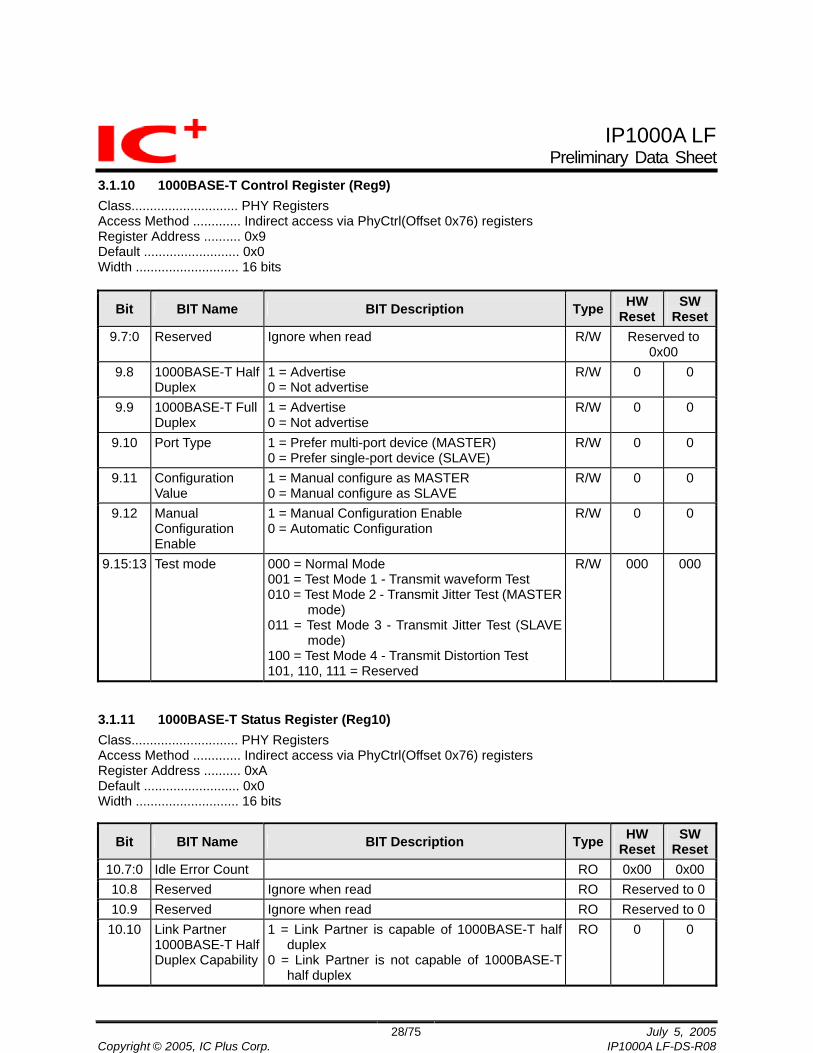
3.1.10 1000BASE-T Control Register (Reg9) Class............................. PHY Registers Access Method ............. Indirect access via PhyCtrl(Offset 0x76) registers Register Address .......... 0x9 Default .......................... 0x0 Width ............................ 16 bits
Bit BIT Name BIT Description Type HW Reset
SW Reset
9.7:0 Reserved Ignore when read R/W Reserved to 0x00
9.8 1000BASE-T Half Duplex
1 = Advertise 0 = Not advertise
R/W 0 0
9.9 1000BASE-T Full Duplex
1 = Advertise 0 = Not advertise
R/W 0 0
9.10 Port Type 1 = Prefer multi-port device (MASTER) 0 = Prefer single-port device (SLAVE)
R/W 0 0
9.11 Configuration Value
1 = Manual configure as MASTER 0 = Manual configure as SLAVE
R/W 0 0
9.12 Manual Configuration Enable
1 = Manual Configuration Enable 0 = Automatic Configuration
R/W 0 0
9.15:13 Test mode 000 = Normal Mode 001 = Test Mode 1 - Transmit waveform Test 010 = Test Mode 2 - Transmit Jitter Test (MASTER
mode) 011 = Test Mode 3 - Transmit Jitter Test (SLAVE
mode) 100 = Test Mode 4 - Transmit Distortion Test 101, 110, 111 = Reserved
R/W 000 000
3.1.11 1000BASE-T Status Register (Reg10) Class............................. PHY Registers Access Method ............. Indirect access via PhyCtrl(Offset 0x76) registers Register Address .......... 0xA Default .......................... 0x0 Width ............................ 16 bits
Bit BIT Name BIT Description Type HW Reset
SW Reset
10.7:0 Idle Error Count RO 0x00 0x0010.8 Reserved Ignore when read RO Reserved to 010.9 Reserved Ignore when read RO Reserved to 0
10.10 Link Partner 1000BASE-T Half Duplex Capability
1 = Link Partner is capable of 1000BASE-T half duplex
0 = Link Partner is not capable of 1000BASE-T half duplex
RO 0 0

IP1000A LF Preliminary Data Sheet
29/75 July 5, 2005Copyright © 2005, IC Plus Corp. IP1000A LF-DS-R08
Bit BIT Name BIT Description Type HW Reset
SW Reset
10.11 Link Partner 1000BASE-T Full Duplex Capability
1 = Link Partner is capable of 1000BASE-T full duplex
0 = Link Partner is not capable of 1000BASE-T full duplex
RO 0 0
10.12 Remote Receiver Status
1 = Remote Receiver OK 0 = Remote Receiver Not OK
RO 0 0
10.13 Local Receiver Status
1 = Local Receiver OK 0 = Local Receiver Not OK
RO 0 0
10.14 MASTER/SLAVE Configuration Resolution
1 = Local PHY configuration resolved to MASTER0 = Local PHY configuration resolved to SLAVE
RO 0 0
10.15 MASTER/SLAVE Configuration Fault
1 = MASTER/SLAVE configuration fault detected0 = No MASTER/SLAVE configuration fault detected
RO LH SC
0 0
3.1.12 Extended Status Register (Reg15) Class............................. PHY Registers Access Method ............. Indirect access via PhyCtrl(Offset 0x76) registers Register Address .......... 0xF Default .......................... 0xC000 Width ............................ 16 bits
Bit BIT Name BIT Description Type HW Reset
SW Reset
15.11:0 Reserved Ignore when read RO 0x000 0x00015.12 1000BASE-T Half
Duplex 1 =PHY able to perform half duplex 1000BASE-T0 =PHY not able to perform half duplex 1000BASE-T
RO 1 1
15.13 1000BASE-T Full Duplex
1 =PHY able to perform full duplex 1000BASE-T 0 =PHY not able to perform full duplex 1000BASE-T
RO 1 1
15.14 1000BASE-X Half Duplex
1 =PHY able to perform half duplex 1000BASE-X0 =PHY not able to perform half duplex 1000BASE-X
RO 0 0
15.15 1000BASE-X Full Duplex
1 =PHY able to perform full duplex 1000BASE-X 0 =PHY not able to perform full duplex 1000BASE-X
RO 0 0

IP1000A LF Preliminary Data Sheet
30/75 July 5, 2005Copyright © 2005, IC Plus Corp. IP1000A LF-DS-R08
3.2 MAC Registers 3.2.1 Ethernet MIB Statistics The host interacts with the IP1000A LF mainly through slave registers, which occupy 256 bytes in the host system’s I/O space, 512 bytes in memory space, or both. Generally, registers are referred to as “I/O registers”, implying that the registers may in fact be mapped and accessed by the host system in memory space. These registers must be accessed with instructions that are no larger than the bit-width of the register being accessed. There are several classes of I/O registers, with Ethernet Management Information Base (MIB) Statistics comprising a portion of the total I/O register space. The Ethernet MIB Statistic registers implement several counters defined in the IEEE 802.3 standard.
Table 3-3 : IP1000A LF Ethernet MIB Statistics Register Map
CLK BYTE 4 BYTE 3 BYTE 2 BYTE 1 ADDR OFFSETTx FramesWEXDeferal FramesAbortXSColls FC Tx MacControlFramesXmtd CarrierSenseErrors F8 Tx BcstFramesXmtdOk F4 Tx SingleColFrames F0 Tx MultiColFrames EC Tx LateCollisions E8 Tx FramesWDeferredXmt E4 Tx McstFramesXmtdOk E0 Tx FramesXmtdOk DC Tx BcstOctetXmtOk D8 Tx McstOctetXmtOk D4 Tx OctetXmtOk D0 Rx FramesLostRxErrors FramesCheckSeqErrors CC Rx InRangeLengthErrors FrameTooLongErrors C8 Rx MacControlFramesRcvd C4 Rx C0 Rx BcstFramesRcvdOk BC Rx McstFramesRcvdOk B8 Rx FramesRcvdOk B4 Rx BcstOctetRcvOk B0 Rx McstOctetRcvdOk AC Rx OctetRcvOk A8

IP1000A LF Preliminary Data Sheet
31/75 July 5, 2005Copyright © 2005, IC Plus Corp. IP1000A LF-DS-R08
3.2.1.1 BcstFramesRcvdOk Class............................. Ethernet MIB Statistics I/O Base Address ......... IoBaseAddress register value Memory Base Address . MemBaseAddress register value Address Offset .............. 0xBC Default Value ................ 0x0000 Access Rule.................. Word Width ............................ 16 bits
Bit BIT Name BIT Description Type HW Reset
SW Reset
15..0 BcstFramesRcvdOk
Broadcast Frames Received OK is the count of the number of frames that are successfully received with destination address equal to the broadcast address (0xFFFFFFFFFFFF).Bcst-FramesRcvdOk does not include frames received with frames too long, FCS, length or alignment errors, or frames lost due to internal MAC sublayer error (i.e. overrun). BcstFramesRcvdOk will wrap around to zero after reaching 0xFFFF. See IEEE 802.3 Clause 30.3.1.1.22. An UpdateStats interrupt (UpdateStats bit within the IntStatus register) will occur when BcstFramesRcvdOk reaches a value of 0xC000. BcstFramesRcvdOk is enabled by writing a logic 1to the StatisticsEnable bit in the MACCtrl register, and a logic 0 to the BcstFramesRcvdOk bit within the StatisticsMask register.
R/W
3.2.1.2 BcstFramesXmtdOk Class............................. Ethernet MIB Statistics I/O Base Address ......... IoBaseAddress register value Memory Base Address . MemBaseAddress register value Address Offset .............. 0xF6 Default Value ................ 0x0000 Access Rule.................. Word Width ............................ 16 bits
Bit BIT Name BIT Description Type HW Reset
SW Reset
15..0 BcstFramesXmtdOk
Broadcast Frames Transmitted is the count of the number of frames that are successfully transmitted to the broadcast address (0xFFFFFFFFFFFF). Frames transmitted to othermulticast addresses are excluded from this statistic. Bcst-FramesXmtdOk will wrap around to zero after reaching 0xFFFF. See IEEE 802.3 Clause 30.3.1.1.19. An UpdateStats interrupt (UpdateStats bit within the IntStatus register) will occur when
R/W
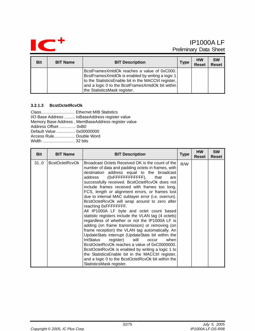
IP1000A LF Preliminary Data Sheet
32/75 July 5, 2005Copyright © 2005, IC Plus Corp. IP1000A LF-DS-R08
Bit BIT Name BIT Description Type HW Reset
SW Reset
BcstFramesXmtdOk reaches a value of 0xC000. BcstFramesXmtdOk is enabled by writing a logic 1to the StatisticsEnable bit in the MACCtrl register, and a logic 0 to the BcstFramesXmtdOk bit within the StatisticsMask register.
3.2.1.3 BcstOctetRcvOk Class............................. Ethernet MIB Statistics I/O Base Address ......... IoBaseAddress register value Memory Base Address . MemBaseAddress register value Address Offset .............. 0xB0 Default Value ................ 0x00000000 Access Rule.................. Double Word Width ............................ 32 bits
Bit BIT Name BIT Description Type HW Reset
SW Reset
31..0 BcstOctetRcvOk Broadcast Octets Received OK is the count of the number of data and padding octets in frames, with destination address equal to the broadcast address (0xFFFFFFFFFFFF), that aresuccessfully received. BcstOctetRcvOk does not include frames received with frames too long, FCS, length or alignment errors, or frames lost due to internal MAC sublayer error (i.e. overrun). BcstOctetRcvOk will wrap around to zero afterreaching 0xFFFFFFFF. All IP1000A LF byte and octet count based statistic registers include the VLAN tag (4 octets) regardless of whether or not the IP1000A LF is adding (on frame transmission) or removing (on frame reception) the VLAN tag automatically. An UpdateStats interrupt (UpdateStats bit within the IntStatus register) will occur when BcstOctetRcvOk reaches a value of 0xC0000000. BcstOctetRcvOk is enabled by writing a logic 1 to the StatisticsEnable bit in the MACCtrl register, and a logic 0 to the BcstOctetRcvOk bit within the StatisticsMask register.
R/W

IP1000A LF Preliminary Data Sheet
33/75 July 5, 2005Copyright © 2005, IC Plus Corp. IP1000A LF-DS-R08
3.2.1.4 BcstOctetXmtOk Class............................. Ethernet MIB Statistics I/O Base Address ......... IoBaseAddress register value Memory Base Address . MemBaseAddress register value Address Offset .............. 0xD8 Default Value ................ 0x00000000 Access Rule.................. Double Word Width ............................ 32 bits
Bit BIT Name BIT Description Type HW Reset
SW Reset
31..0 BcstOctetXmtOk Broadcast Octets Transmitted OK is a count of data and padding octets of frames successfully transmitted to a the broadcast address (0xFFFFFFFFFFFF). BcstOctetXmtOk will wraparound to zero after reaching 0xFFFFFFFF. All IP1000A LF byte and octet count based statistic registers include the VLAN tag (4 octets) regardless of whether or not the IP1000A LF is adding (on frame transmission) or removing (on frame reception) the VLAN tag automatically. An UpdateStats interrupt (UpdateStats bit within the IntStatus register) will occur when BcstOctetXmtOk reaches a value of 0xC0000000. BcstOctetXmtOk is enabled by writing a logic 1 to the StatisticsEnable bit in the MACCtrl register, and a logic 0 to the BcstOctetXmtOk bit within the StatisticsMask register.
R/W
3.2.1.5 CarrierSenseErrors Class............................. Ethernet MIB Statistics I/O Base Address ......... IoBaseAddress register value Memory Base Address . MemBaseAddress register value Address Offset .............. 0xF8 Default Value ................ 0x0000 Access Rule.................. Word Width ............................ 16 bits
Bit BIT Name BIT Description Type HW Reset
SW Reset
15..0 CarrierSenseErrors Carrier Sense Errors counts the number of times that the carrier sense signal (CRS) was de-asserted (a logic 0) during the transmission of a frame without collision. The carrier sense signal is not monitored for the purpose of this statistic until after the preamble and start-of-frame delimiter fields of the Ethernet frame have been transmitted. CarrierSenseErrors will wrap around to zero after reaching 0xFFFF. See IEEE 802.3Clause 30.3.1.1.13. An UpdateStats interrupt (UpdateStats bit within
R/W

IP1000A LF Preliminary Data Sheet
34/75 July 5, 2005Copyright © 2005, IC Plus Corp. IP1000A LF-DS-R08
Bit BIT Name BIT Description Type HW Reset
SW Reset
the IntStatus register) will occur when CarrierSenseErrors reaches a value of 0xC000. CarrierSenseErrors is enabled by writing a logic 1to the StatisticsEnable bit in the MACCtrl register, and a logic 0 to the CarrierSenseErrors bit within the StatisticsMask register.
3.2.1.6 FramesAbortXSColls Class............................. Ethernet MIB Statistics I/O Base Address ......... IoBaseAddress register value Memory Base Address . MemBaseAddress register value Address Offset .............. 0xFC Default Value ................ 0x0000 Access Rule.................. Word Width ............................ 16 bits
Bit BIT Name BIT Description Type HW Reset
SW Reset
15..0 FramesAbortXS-Colls
Frames Aborted Due to Excess Collisions counts the number of frames which are not transmitted successfully due to excessive collisions. FramesAbortXSColls will wrap around to zeroafter reaching 0xFFFF. See IEEE 802.3 Clause 30.3.1.1.11. An UpdateStats interrupt (UpdateStats bit within the IntStatus register) will occur when FramesAbortXSColls reaches a value of 0xC000. FramesAbortXSColls is enabled by writing a logic 1 to the StatisticsEnable bit in the MACCtrl register, and a logic 0 to the FramesAbortXSColls bit within the StatisticsMask register.
R/W

IP1000A LF Preliminary Data Sheet
35/75 July 5, 2005Copyright © 2005, IC Plus Corp. IP1000A LF-DS-R08
3.2.1.7 FramesCheckSeqErrors Class............................. Ethernet MIB Statistics I/O Base Address ......... IoBaseAddress register value Memory Base Address . MemBaseAddress register value Address Offset .............. 0xCC Default Value ................ 0x0000 Access Rule.................. Word Width ............................ 16 bits
Bit BIT Name BIT Description Type HW Reset
SW Reset
15..0 FramesCheckSeqErrors
Frame Check Sequence Errors is a count of received frames that are an integral number of octets in length and do not pass the FCS check. This does not include frames received withframe-too-long, or frame-too-short (runt) errors. FramesCheck-SeqErrors will wrap around to zero after reaching 0xFFFF. See IEEE 802.3 Clause 30.3.1.1.6. An UpdateStats interrupt (UpdateStats bit within the IntStatus register) will occur when FramesCheckSeqErrors reaches a value of 0xC000. FramesCheckSeqErrors is enabled by writing a logic 1 to the StatisticsEnable bit in the MACCtrl register, and a logic 0 to the FramesCheckSeqErrors bit within the StatisticsMask register.
R/W
3.2.1.8 FramesLostRxErrors Class............................. Ethernet MIB Statistics I/O Base Address ......... IoBaseAddress register value Memory Base Address . MemBaseAddress register value Address Offset .............. 0xCE Default Value ................ 0x0000 Access Rule.................. Word Width ............................ 16 bits
Bit BIT Name BIT Description Type HW Reset
SW Reset
15..0 FramesLostRx-Errors
Frames Lost Due to Receive Errors is a count of the number of frames that should have been received (the destination address matched the filter criteria) but experienced a receive FIFO overrun error (the receive FIFO does not have enough free space to store the received data). FramesLostRxErrors only includes overruns that become apparent to the host system, and does not include frames that are completely ignoreddue to a completely full receive FIFO at the beginning of frame reception. FramesLostRxErrors will wrap around to zero
R/W

IP1000A LF Preliminary Data Sheet
36/75 July 5, 2005Copyright © 2005, IC Plus Corp. IP1000A LF-DS-R08
Bit BIT Name BIT Description Type HW Reset
SW Reset
after reaching 0xFFFF. See IEEE 802.3 Clause 30.3.1.1.15. An UpdateStats interrupt (UpdateStats bit within the IntStatus register) will occur when FramesLostRxErrors reaches a value of 0xC000. FramesLostRxErrors is enabled by writing a logic 1 to the StatisticsEnable bit in the MACCtrl register, and a logic 0 to the FramesLostRxErrors bit within the StatisticsMask register.
3.2.1.9 FramesRcvdOk Class............................. Ethernet MIB Statistics I/O Base Address ......... IoBaseAddress register value Memory Base Address . MemBaseAddress register value Address Offset .............. 0xB4 Default Value ................ 0x00000000 Access Rule.................. Double Word Width ............................ 32 bits
Bit BIT Name BIT Description Type HW Reset
SW Reset
31..0 FramesRcvdOk Frames Received OK is the count of the number of frames that are successfully received. FramesRcvdOk does not include frames received with frames too long, FCS, length or alignment errors, or frames lost due to internal MAC sublayer error (i.e. overrun). FramesRcvdOk will wrap around to zero after reaching 0xFFFFFFFF. See IEEE 802.3 Clause 30.3.1.1.5.An UpdateStats interrupt (UpdateStats bit within the IntStatus register) will occur when FramesRcvdOk reaches a value of 0xC0000000. FramesRcvdOk is enabled by writing a logic 1 tothe StatisticsEnable bit in the MACCtrl register, and a logic 0 to the FramesRcvdOk bit within the StatisticsMask register.
R/W

IP1000A LF Preliminary Data Sheet
37/75 July 5, 2005Copyright © 2005, IC Plus Corp. IP1000A LF-DS-R08
3.2.1.10 FramesWDeferredXmt Class............................. Ethernet MIB Statistics I/O Base Address ......... IoBaseAddress register value Memory Base Address . MemBaseAddress register value Address Offset .............. 0xE4 Default Value ................ 0x00000000 Access Rule.................. Double Word Width ............................ 32 bits
Bit BIT Name BIT Description Type HW Reset
SW Reset
31..0 FramesWDeferredXmt
Frames with Deferred Transmit is a count of the number of frames that must delay their first attempt of transmission because the medium was busy. Frames involved in any collisions are not counted by FramesWDeferredXmt. FramesWDeferredXmtwrap around to zero after reaching 0xFFFFFFFF.See IEEE 802.3 Clause 30.3.1.1.9. An UpdateStats interrupt (UpdateStats bit within the IntStatus register) will occur when FramesWDeferredXmt reaches a value of 0xC0000000. FramesWDeferredXmt is enabled bywriting a logic 1 to the StatisticsEnable bit in the MACCtrl register, and a logic 0 to the FramesWDeferredXmt bit within the StatisticsMask register.
R/W
3.2.1.11 FramesWEXDeferal Class............................. Ethernet MIB Statistics I/O Base Address ......... IoBaseAddress register value Memory Base Address . MemBaseAddress register value Address Offset .............. 0xFE Default Value ................ 0x0000 Access Rule.................. Word Width ............................ 16 bits
Bit BIT Name BIT Description Type HW Reset
SW Reset
15..0 FramesWEXDe-feral
Frames with Excessive Deferals counts the number of frames that deferred for an excessive period of time (exceeding the defer limit). FramesWEXDeferal is only incremented once perLLC frame. FramesWEXDeferal will wrap around to zero after reaching 0xFFFF. See IEEE 802.3 Clause 30.3.1.1.20. An UpdateStats interrupt (UpdateStats bit within the IntStatus register) will occur when FramesWEXDeferal reaches a value of 0xC000. FramesWEXDeferal is enabled by writing a logic 1to the StatisticsEnable bit in the MACCtrl register, and a logic 0 to the FramesWEXDeferal bit within the StatisticsMask register.
R/W

IP1000A LF Preliminary Data Sheet
38/75 July 5, 2005Copyright © 2005, IC Plus Corp. IP1000A LF-DS-R08
3.2.1.12 FramesXmtdOk Class............................. Ethernet MIB Statistics I/O Base Address ......... IoBaseAddress register value Memory Base Address . MemBaseAddress register value Address Offset .............. 0xDC Default Value ................ 0x00000000 Access Rule.................. Double Word Width ............................ 32 bits
Bit BIT Name BIT Description Type HW Reset
SW Reset
31..0 FramesXmtdOk Frames Transmitted OK is a count of the number of frames that are successfully transmitted. FramesXmtdOk will wrap around to zero after reaching 0xFFFFFFFF. See IEEE 802.3 Clause 30.3.1.1.2. An UpdateStats interrupt (UpdateStats bit within the IntStatus register) will occur when FramesXmtdOk reaches a value of 0xC0000000. FramesXmtdOk is enabled by writing a logic 1 tothe StatisticsEnable bit in the MACCtrl register, and a logic 0 to the FramesXmtdOk bit within the StatisticsMask register.
R/W
3.2.1.13 FrameTooLongErrors Class............................. Ethernet MIB Statistics I/O Base Address ......... IoBaseAddress register value Memory Base Address . MemBaseAddress register value Address Offset .............. 0xC8 Default Value ................ 0x0000 Access Rule.................. Word Width ............................ 16 bits
Bit BIT Name BIT Description Type HW Reset
SW Reset
15..0 FrameTooLong-Errors
Frame Too Long Errors is a count of frames received whose length exceed the value in the MaxFrameSize register. FrameTooLongErrors will wrap around to zero after reaching 0xFFFF. See IEEE 802.3 Clause 30.3.1.1.25. An UpdateStats interrupt (UpdateStats bit within the IntStatus register) will occur when FrameTooLongErrors reaches a value of 0xC000. FrameTooLongErrors is enabled by writing a logic1 to the StatisticsEnable bit in the MACCtrl register, and a logic 0 to the FrameTooLongErrors bit within the StatisticsMask register.
R/W

IP1000A LF Preliminary Data Sheet
39/75 July 5, 2005Copyright © 2005, IC Plus Corp. IP1000A LF-DS-R08
3.2.1.14 InRangeLengthErrors Class............................. Ethernet MIB Statistics I/O Base Address ......... IoBaseAddress register value Memory Base Address . MemBaseAddress register value Address Offset .............. 0xCA Default Value ................ 0x0000 Access Rule.................. Word Width ............................ 16 bits
Bit BIT Name BIT Description Type HW Reset
SW Reset
15..0 InRangeLengthErrors
In Range Length Errors is a count of the number of frames with the Length/Type field value between the minimum unpadded MAC client data size and the maximum allowed MAC client data size, inclusive, that does not match the number of MAC client data octets received. InRangeLengthErrors also increments for frames whose Length/Type field value is less than the minimum allowed unpadded MAC client data size, and the number of MAC client data octets received is greater than the minimum unpadded MAC client data size. InRangeLengthErrors will wrap around to zero after reaching 0xFFFF. See IEEE 802.3 Clause 30.3.1.1.23. An UpdateStats interrupt (UpdateStats bit within the IntStatus register) will occur when InRangeLengthErrors reaches a value of 0xC000. InRangeLengthErrors is enabled by writing a logic 1 to the StatisticsEnable bit in the MACCtrl register, and a logic 0 to the InRangeLengthErrors bit within the StatisticsMask register.
R/W
3.2.1.15 LateCollisions Class............................. Ethernet MIB Statistics I/O Base Address ......... IoBaseAddress register value Memory Base Address . MemBaseAddress register value Address Offset .............. 0xE8 Default Value ................ 0x00000000 Access Rule.................. Double Word Width ............................ 32 bits
Bit BIT Name BIT Description Type HW Reset
SW Reset
31..0 LateCollisions Late Collisions is a count of the number of times that a collision has been detected later than 1 slot time into the transmitted frame. LateCollisions will wrap around to zero after reaching 0xFFFFFFFF. See IEEE 802.3 Clause 30.3.1.1.10. An UpdateStats interrupt (UpdateStats bit within the IntStatus register) will occur when
R/W

IP1000A LF Preliminary Data Sheet
40/75 July 5, 2005Copyright © 2005, IC Plus Corp. IP1000A LF-DS-R08
Bit BIT Name BIT Description Type HW Reset
SW Reset
LateCollisions reaches a value of 0xC0000000. LateCollisions is enabled by writing a logic 1 to the StatisticsEnable bit in the MACCtrl register, and a logic 0 to the LateCollisions bit within the StatisticsMask register.
3.2.1.16 MacControlFramesRcvd Class............................. Ethernet MIB Statistics I/O Base Address ......... IoBaseAddress register value Memory Base Address . MemBaseAddress register value Address Offset .............. 0xC6 Default Value ................ 0x0000 Access Rule.................. Word Width ............................ 16 bits
Bit BIT Name BIT Description Type HW Reset
SW Reset
15..0 MacControl-FramesRcvd
MAC Control Frames Received is a count of the number of MAC control PAUSE frames, and only PAUSE frames, received successfully. MacControlFramesRcvd will wrap around to zero after reaching 0xFFFF. An UpdateStats interrupt (UpdateStats bit within the IntStatus register) will occur when MacControlFramesRcvd reaches a value of 0xC000. MacControlFramesRcvd is enabled by writing a logic 1 to the StatisticsEnable bit in the MACCtrl register, and a logic 0 to the MacControlFramesRcvd bit within the StatisticsMask register.
R/W

IP1000A LF Preliminary Data Sheet
41/75 July 5, 2005Copyright © 2005, IC Plus Corp. IP1000A LF-DS-R08
3.2.1.17 MacControlFramesXmtd Class............................. Ethernet MIB Statistics I/O Base Address ......... IoBaseAddress register value Memory Base Address . MemBaseAddress register value Address Offset .............. 0xFA Default Value ................ 0x0000 Access Rule.................. Word Width ............................ 16 bits
Bit BIT Name BIT Description Type HW Reset
SW Reset
15..0 MacControl-FramesXmtd
MAC Control Frames Transmitted is the count of MAC control frames transmitted by the IP1000A LF. Note, acControl-FramesXmtd does not include MAC control frames transferred to the IP1000A LF by the host system via the transmit DMA process.An UpdateStats interrupt (UpdateStats bit within the IntStatus register) will occur when MacControlFramesXmtd reaches a value of 0xC000. MacControlFramesXmtd is enabled by writing a logic 1 to the StatisticsEnable bit in the MACCtrl register, and a logic 0 to the MacControlFramesXmtd bit within the StatisticsMask register.
R/W
3.2.1.18 McstFramesRcvdOk Class............................. Ethernet MIB Statistics I/O Base Address ......... IoBaseAddress register value Memory Base Address . MemBaseAddress register value Address Offset .............. 0xB8 Default Value ................ 0x00000000 Access Rule.................. Double Word Width ............................ 32 bits
Bit BIT Name BIT Description Type HW Reset
SW Reset
31..0 McstFramesRcvdOk
Broadcast Frames Received OK is the count of the number of frames that are successfully received to a group destination address other than the broadcast address (0xFFFFFFFFFFFF). McstFramesRcvdOk does not include frames received with frames too long, FCS, length or alignment errors, or frames lost due to internal MAC sublayer error (i.e. overrun). McstFramesRcvdOk will wrap around to zero after reaching 0xFFFFFFFF. See IEEE 802.3 Clause30.3.1.1.21. An UpdateStats interrupt (UpdateStats bit within the IntStatus register) will occur when McstFramesRcvdOk reaches a value of 0xC0000000. McstFramesRcvdOk is enabled by writing a logic 1 to the StatisticsEnable bit in the
R/W

IP1000A LF Preliminary Data Sheet
42/75 July 5, 2005Copyright © 2005, IC Plus Corp. IP1000A LF-DS-R08
Bit BIT Name BIT Description Type HW Reset
SW Reset
MACCtrl register, and a logic 0 to the McstFramesRcvdOk bit within the StatisticsMaskregister.
3.2.1.19 McstFramesXmtdOk Class............................. Ethernet MIB Statistics I/O Base Address ......... IoBaseAddress register value Memory Base Address . MemBaseAddress register value Address Offset .............. 0xE0 Default Value ................ 0x00000000 Access Rule.................. Double Word Width ............................ 32 bits
Bit BIT Name BIT Description Type HW Reset
SW Reset
31..0 McstFramesXmtdOk
Multicast Frames Transmitted OK is a count of the number of frames that are successfully transmitted to a group destination address other than the broadcast address (0xFFFFFFFFFFFF). McstFramesXmtdOk will wrap around to zero after reaching 0xFFFFFFFF. See IEEE 802.3 Clause30.3.1.1.18. An UpdateStats interrupt (UpdateStats bit within the IntStatus register) will occur when McstFramesXmtdOk reaches a value of 0xC0000000. McstFramesXmtdOk is enabled by writing a logic 1 to the StatisticsEnable bit in the MACCtrl register, and a logic 0 to the McstFramesXmtdOk bit within the StatisticsMaskregister.
R/W
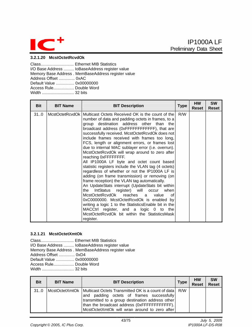
IP1000A LF Preliminary Data Sheet
43/75 July 5, 2005Copyright © 2005, IC Plus Corp. IP1000A LF-DS-R08
3.2.1.20 McstOctetRcvdOk Class............................. Ethernet MIB Statistics I/O Base Address ......... IoBaseAddress register value Memory Base Address . MemBaseAddress register value Address Offset .............. 0xAC Default Value ................ 0x00000000 Access Rule.................. Double Word Width ............................ 32 bits
Bit BIT Name BIT Description Type HW Reset
SW Reset
31..0 McstOctetRcvdOk Multicast Octets Received OK is the count of the number of data and padding octets in frames, to a group destination address other than the broadcast address (0xFFFFFFFFFFFF), that are successfully received. McstOctetRcvdOk does not include frames received with frames too long, FCS, length or alignment errors, or frames lost due to internal MAC sublayer error (i.e. overrun). McstOctetRcvdOk will wrap around to zero after reaching 0xFFFFFFFF. All IP1000A LF byte and octet count based statistic registers include the VLAN tag (4 octets) regardless of whether or not the IP1000A LF is adding (on frame transmission) or removing (on frame reception) the VLAN tag automatically. An UpdateStats interrupt (UpdateStats bit within the IntStatus register) will occur when McstOctetRcvdOk reaches a value of0xC0000000. McstOctetRcvdOk is enabled by writing a logic 1 to the StatisticsEnable bit in the MACCtrl register, and a logic 0 to the McstOctetRcvdOk bit within the StatisticsMask register.
R/W
3.2.1.21 McstOctetXmtOk Class............................. Ethernet MIB Statistics I/O Base Address ......... IoBaseAddress register value Memory Base Address . MemBaseAddress register value Address Offset .............. 0xD4 Default Value ................ 0x00000000 Access Rule.................. Double Word Width ............................ 32 bits
Bit BIT Name BIT Description Type HW Reset
SW Reset
31..0 McstOctetXmtOk Multicast Octets Transmitted OK is a count of data and padding octets of frames successfully transmitted to a group destination address other than the broadcast address (0xFFFFFFFFFFFF). McstOctetXmtOk will wrap around to zero after
R/W

IP1000A LF Preliminary Data Sheet
44/75 July 5, 2005Copyright © 2005, IC Plus Corp. IP1000A LF-DS-R08
Bit BIT Name BIT Description Type HW Reset
SW Reset
reaching 0xFFFFFFFF. All IP1000A LF byte and octet count based statistic registers include the VLAN tag (4 octets) regardless of whether or not the IP1000A LF is adding (on frame transmission) or removing (on frame reception) the VLAN tag automatically. An UpdateStats interrupt (UpdateStats bit within the IntStatus register) will occur when McstOctetXmtOk reaches a value of 0xC0000000. McstOctetXmtOk is enabled by writing a logic 1 to the StatisticsEnable bit in the MACCtrl register, and a logic 0 to the McstOctetXmtOk bit within the StatisticsMask register.
3.2.1.22 MultiColFrames Class............................. Ethernet MIB Statistics I/O Base Address ......... IoBaseAddress register value Memory Base Address . MemBaseAddress register value Address Offset .............. 0xEC Default Value ................ 0x00000000 Access Rule.................. Double Word Width ............................ 32 bits
Bit BIT Name BIT Description Type HW Reset
SW Reset
31..0 MultiColFrames Multiple Collision Frames is a count of the number of frames that are involved in more than one collision and are subsequently transmitted successfully. MultiColFrames will wrap around to zero after reaching 0xFFFFFFFF. See IEEE 802.3Clause 30.3.1.1.4. An UpdateStats interrupt (UpdateStats bit within the IntStatus register) will occur when MultiColFrames reaches a value of 0xC0000000. MultiColFrames is enabled by writing a logic 1 tothe StatisticsEnable bit in the MACCtrl register, and a logic 0 to the MultiColFrames bit within the StatisticsMask register.
R/W
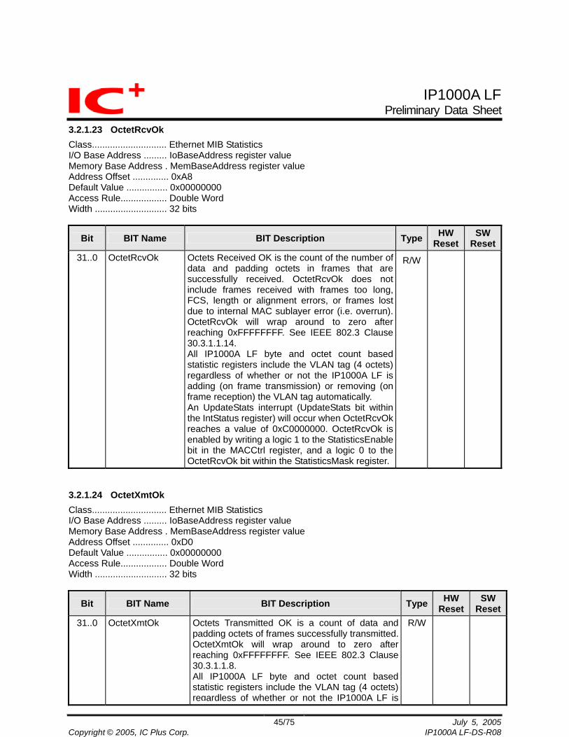
IP1000A LF Preliminary Data Sheet
45/75 July 5, 2005Copyright © 2005, IC Plus Corp. IP1000A LF-DS-R08
3.2.1.23 OctetRcvOk Class............................. Ethernet MIB Statistics I/O Base Address ......... IoBaseAddress register value Memory Base Address . MemBaseAddress register value Address Offset .............. 0xA8 Default Value ................ 0x00000000 Access Rule.................. Double Word Width ............................ 32 bits
Bit BIT Name BIT Description Type HW Reset
SW Reset
31..0 OctetRcvOk Octets Received OK is the count of the number of data and padding octets in frames that are successfully received. OctetRcvOk does not include frames received with frames too long, FCS, length or alignment errors, or frames lost due to internal MAC sublayer error (i.e. overrun). OctetRcvOk will wrap around to zero after reaching 0xFFFFFFFF. See IEEE 802.3 Clause 30.3.1.1.14. All IP1000A LF byte and octet count based statistic registers include the VLAN tag (4 octets) regardless of whether or not the IP1000A LF is adding (on frame transmission) or removing (on frame reception) the VLAN tag automatically. An UpdateStats interrupt (UpdateStats bit within the IntStatus register) will occur when OctetRcvOk reaches a value of 0xC0000000. OctetRcvOk is enabled by writing a logic 1 to the StatisticsEnable bit in the MACCtrl register, and a logic 0 to theOctetRcvOk bit within the StatisticsMask register.
R/W
3.2.1.24 OctetXmtOk Class............................. Ethernet MIB Statistics I/O Base Address ......... IoBaseAddress register value Memory Base Address . MemBaseAddress register value Address Offset .............. 0xD0 Default Value ................ 0x00000000 Access Rule.................. Double Word Width ............................ 32 bits
Bit BIT Name BIT Description Type HW Reset
SW Reset
31..0 OctetXmtOk Octets Transmitted OK is a count of data and padding octets of frames successfully transmitted. OctetXmtOk will wrap around to zero afterreaching 0xFFFFFFFF. See IEEE 802.3 Clause30.3.1.1.8. All IP1000A LF byte and octet count based statistic registers include the VLAN tag (4 octets) regardless of whether or not the IP1000A LF is
R/W

IP1000A LF Preliminary Data Sheet
46/75 July 5, 2005Copyright © 2005, IC Plus Corp. IP1000A LF-DS-R08
Bit BIT Name BIT Description Type HW Reset
SW Reset
adding (on frame transmission) or removing (on frame reception) the VLAN tag automatically. An UpdateStats interrupt (UpdateStats bit within the IntStatus register) will occur when OctetXmtOk reaches a value of 0xC0000000. OctetXmtOk is enabled by writing a logic 1 to theStatisticsEnable bit in the MACCtrl register, and a logic 0 to the OctetXmtOk bit within the StatisticsMask register.
3.2.1.25 SingleColFrames Class............................. Ethernet MIB Statistics I/O Base Address ......... IoBaseAddress register value Memory Base Address . MemBaseAddress register value Address Offset .............. 0xF0 Default Value ................ 0x00000000 Access Rule.................. Double Word Width ............................ 32 bits
Bit BIT Name BIT Description Type HW Reset
SW Reset
31..0 SingleColFrames Single Collision Frames is a count of the number of frames that are involved in a single collision, and are subsequently transmitted successfully. SingleColFrames will wrap around to zero after reaching 0xFFFFFFFF. See IEEE 802.3 Clause30.3.1.1.3. An UpdateStats interrupt (UpdateStats bit within the IntStatus register) will occur when SingleColFrames reaches a value of0xC0000000. SingleColFrames is enabled by writing a logic 1 to the StatisticsEnable bit in the MACCtrl register, and a logic 0 to the SingleColFrames bit within the StatisticsMask register.
R/W

IP1000A LF Preliminary Data Sheet
47/75 July 5, 2005Copyright © 2005, IC Plus Corp. IP1000A LF-DS-R08
3.2.2 PCI Configuration Space Registers 3.2.2.1 CapId0 Class............................. PCI Configuration Registers, Power Management I/O Base Address ......... PCI device configuration header start Address Offset .............. 0x50 Default Value ................ 0x01 Access Rule.................. Byte Width ............................ 8 bits
Bit BIT Name BIT Description Type HW Reset
SW Reset
7..0 CapId Capabilities ID. CapId indicates the type of the capability data structure for the IP1000A LF. CapId is set to the value 0x01 to indicate a PCI Power Management structure.
R
3.2.2.2 CapId1 Class............................. PCI Configuration Registers, Power Management I/O Base Address ......... PCI device configuration header start Address Offset .............. 0x60 Default Value ................ 0x07 Access Rule.................. Byte Width ............................ 8 bits
Bit BIT Name BIT Description Type HW Reset
SW Reset
7..0 CapId Capabilities ID. CapId indicates the type of the capability data structure for the IP1000A LF.
R
3.2.2.3 CapPtr Class............................. PCI Configuration Registers I/O Base Address ......... PCI device configuration header start Address Offset .............. 0x34 Default Value ................ 0x50 Access Rule.................. Byte Width ............................ 8 bits
Bit BIT Name BIT Description Type HW Reset
SW Reset
7..0 CapPtr Capabilities Pointer. CapPtr indicates the beginning of a chain of registers which describe enhanced functions. CapPtr register returns 0x50, which is the address of the first in a series ofpower management registers.
R

IP1000A LF Preliminary Data Sheet
48/75 July 5, 2005Copyright © 2005, IC Plus Corp. IP1000A LF-DS-R08
3.2.2.4 ClassCode Class............................. PCI Configuration Registers I/O Base Address ......... PCI device configuration header start Address Offset .............. 0x09 Default Value ................ 0x020000 Access Rule.................. Byte Width ............................ 24 bits
Bit BIT Name BIT Description Type HW Reset
SW Reset
23..0 ClassCode Class Code. ClassCode identifies the general function of the PCI device. A value of 0x020000 indicates an Ethernet network controller.
R
3.2.2.5 ConfigCommand Class............................. PCI Configuration Registers I/O Base Address ......... PCI device configuration header start Address Offset .............. 0x04 Default Value ................ 0x0000 Access Rule.................. Word Width ............................ 16 bits ConfigCommand provides control over the IP1000A LF’s ability to generate and respond to PCI cycles. When ConfigCommand is a logic 0, the IP1000A LF is logically disconnected from the PCI bus, except for configuration cycles.
Bit BIT Name BIT Description Type HW Reset
SW Reset
0 IoSpace I/O Space. When IoSpace is a logic the IP1000A LF can respond to I/ O space accesses (if the IP1000A LF is in the D0 power state).
R/W
1 MemorySpace Memory Space. When MemorySpace, and the AddressDecodeEnable bit in the ExpRomBaseAddress register are both a logic 1, and if the IP1000A LF is in the D0 power state, the IP1000A LF is able to decode accesses to an Expansion ROM (if present).
R/W
2 BusMaster Bus Master. When BusMaster is a logic 1 the IP1000A LF is able to initiate bus master cycles (if the adapter is in the D0 power state).
R/W
3 SpecialCycles Special Cycles. When SpecialCycles is a logic 0, the IP1000A LF ignores all Special Cycle operations. When SpecialCycles is a logic 1, the IP1000A LF can monitor Special Cycle operations.
R
4 MWlEnable Memory Write and Invalidate Enable. When MWlEnable is a logic 1 the IP1000A LF is permitted to use the MWI command.
R/W

IP1000A LF Preliminary Data Sheet
49/75 July 5, 2005Copyright © 2005, IC Plus Corp. IP1000A LF-DS-R08
Bit BIT Name BIT Description Type HW Reset
SW Reset
5 VGAPaletteSnoop VGA Palette Snoop. VGAPaletteSnoop controls how VGA compatible graphics devices handle accesses to VGA palette registers. When VGAPaletteSnoop is a logic 1, palette snooping is enabled (i.e., the device does not respond to palette reg-ister writes and snoops the data). When VGAPaletteSnoop is a logic 0, the device should treat palette write accesses like all other accesses.
R
6 ParityErrorResponse Parity Error Response. When ParityErrorResponse is a logic 1 the IP1000A LF responds to parity errors as defined within the PCI specification. When ParityErrorResponse is a logic 0, the IP1000A LF ignores parity errors.
R/W
7 SteppingControl Stepping Control. SteppingControl determines whether or not a device does address/data stepping. Devices that never do stepping must hardwire SteppingControl to a logic 0. Devicesthat always do stepping must hardwire SteppingControl to a logic 1.
R
8 SERREnable System Error Enable. When SERREnable is a logic 1, the SERRN signal is allowed to transition as appropriate. When SERREnable is a logic 0, the SERRN signal is a continuous logic 0.
R/W
9 FastBack-to-BackEnable
Fast Back-to-Back Enable. FastBack-to-BackEnable controls whether or not a master can do fast back-to-back transactions to different devices. Initialization software will set FastBack-to-Back-Enable if all targets are fast back-to-back capable. If Fast-Back-to-BackEnable is a logic 1, the master is allowed to generate fast back-to-back transactions to different agents. If FastBack-to-BackEnable is a logic 0, fast back-to-back transactions are only allowed to the same agent.
R
10 InterruptDisable Interrupt Disable. InterruptDisable disables the IP1000A LF from asserting INTAN. If InterruptDisable is a logic 0, the IP1000A LF mayassert the INTAN signal. If InterruptDisable is a logic 1, the IP1000A LF may not assert the INTAN signal.
R/W
15..11 Reserved Reserved for future use. Write as zero, ignore on read. N/A

IP1000A LF Preliminary Data Sheet
50/75 July 5, 2005Copyright © 2005, IC Plus Corp. IP1000A LF-DS-R08
3.2.2.6 ConfigStatus Class............................. PCI Configuration Registers I/O Base Address ......... PCI device configuration header start Address Offset .............. 0x06 Default Value ................ 0x0230 Access Rule.................. Word Width ............................ 16 bits ConfigStatus is used to record status information for PCI bus events. Read/write bits within ConfigStatus can only be set to a logic 0, not to a logic 1. Bits are set to a logic 0 by writing a logic 1 to the appropriate bit.
Bit BIT Name BIT Description Type HW Reset
SW Reset
2..0 Reserved Reserved for future use. Write as zero, ignore on read. N/A 3 IntStatus Interrupt Status. IntStatus reflects the state of the
interrupt of the IP1000A LF. Only when the Interrupt Disable bit in the command register is a logic 0 and IntStatus is a logic 1, will the IP1000A LF’s INTAN signal be asserted. Setting the Interrupt Disable bit to a 1 has no effect on the state of IntStatus.
R
4 CapabilitiesList Capabilities List. CapabilitiesList is a logic 1 to indicate a set of extended capabilities registers exists for the IP1000A LF. The CapPtr register indicates the first address location of the extendedcapabilities register set.
R
5 66MHzCapable 66MHz Capable. When 66MHzCapable is a logic 1 operation of the IP1000A LF PCI bus interface at 66MHz is supported.
R
6 Reserved Reserved for future use. Write as zero, ignore on read. N/A 7 FastBackToBack Fast Back to Back. When FastBackToBack is a
logic 1 the IP1000A LF when operating as a Target, supports fast back-to-back transactions as defined by the criteria in the section 3.4.2 of the PCI specification.
R
8 MasterDataParityError
Master Data Parity Error. When MasterDataParityError is a logic 1, the IP1000A LF when operating as a Master, has detected the PERRN signal asserted, and the ParityErrorResponse bit in the ConfigCommand register as a logic 1. Note: If the IP1000A LF is initialized to PCI-X mode, MasterDataPari-tyError is set in either the initiator or target under the following conditions:The initiator (requester) of a read transaction that is completed immediately calculates a data parity error. The initiator (requester) of a read transaction that is terminated with Split Response calculates a data parity error in the Split Response. The initiator (requester) of a write that is comleted immediately observes PERRN asserted three clocks after one or more of its data phases. The initiator (requester) of a write that is
R

IP1000A LF Preliminary Data Sheet
51/75 July 5, 2005Copyright © 2005, IC Plus Corp. IP1000A LF-DS-R08
Bit BIT Name BIT Description Type HW Reset
SW Reset
terminated with Split Response observes PERRN asserted three clocks after the data phase. The target (requester) of a Split Completioncalculates a data parity error in either read data or a Split Completion Message. The target (requester) receives a Split Completion Message that indicates a data parity error occurred on one of this device’s non-posted write transactions.
10..9 DevselTiming Device Select Timing. DevselTiming is used to encode the slowest time with which the IP1000A LF asserts the DEVSELN signal. A value of 0x1 for DevselTiming indicates support for “medium” speed DEVSELN assertion.
R
11 SignaledTarget-Abort
Signaled Target Abort. The IP1000A LF sets SignaledTargetAbort to a logic 1 when the IP1000A LF terminates a bus transaction with target-abort.
R
12 ReceivedTarget-Abort
Received Target Abort. The IP1000A LF sets ReceivedTargetAbort to a logic 1 when, operating as a bus master, an IP1000A LF bus transaction is terminated with target-abort.
R
13 ReceivedMaster-Abort
Received Master Abort. The IP1000A LF sets ReceivedMasterAbort to a logic 1 when, operating as a bus master, an IP1000A LF bus transaction is terminated with master-abort.
R
14 SignaledSystem-Error
Signaled System Error. When SignaledSystemError is a logic 1, the IP1000A LF asserts the SERRN signal.
R
15 DetectedParity-Error
Detected Parity Error. When DetectedParityError is a logic 1 the IP1000A LF has detected a parity error, regardless of whether parity error handling is enabled.
R

IP1000A LF Preliminary Data Sheet
52/75 July 5, 2005Copyright © 2005, IC Plus Corp. IP1000A LF-DS-R08
3.2.2.7 Data Class............................. PCI Configuration Registers I/O Base Address ......... PCI device configuration header start Address Offset .............. 0x57 Default Value ................ 0x0000 Access Rule.................. Byte Width ............................ 8 bits
Bit BIT Name BIT Description Type HW Reset
SW Reset
7..0 Data Data reports power consumption and dissipation of the IP1000A LF at worst case conditions. To properly interpret the value read from Data, it must be scaled by the factor indicated in theData_Scale field of the PowerMgmtCtrl register. The value of Data depends on the value of the Data_Select field of the PowerMgmtCtrl register..
Data_Select Data 0x0 40*Data_Scale Watts D0
Power Consumption 0x1 40*Data_Scale Watts D1
Power Consumption 0x2 40*Data_Scale Watts D2
Power Consumption 0x3 40*Data_Scale Watts D3
Power Consumption 0x4 40*Data_Scale Watts D4
Power Consumption 0x5 40*Data_Scale Watts D5
Power Consumption 0x6 40*Data_Scale Watts D6
Power Consumption 0x7 40*Data_Scale Watts D7
Power Consumption 0x8 through
0xF 0x00 Reserved.
R
3.2.2.8 DeviceId Class............................. PCI Configuration Registers I/O Base Address ......... PCI device configuration header start Address Offset .............. 0x02 Access Rule.................. Word Default Value ................ 0x1023 Width ............................ 16 bits
Bit BIT Name BIT Description Type HW Reset
SW Reset
15..0 DeviceId Device ID. DeviceId contains the 16-bit device identifier for the IP1000A LF. The DeviceId may also be modified using the ForcedConfig[1..0] bits in the AsicCtrl register.
R/W
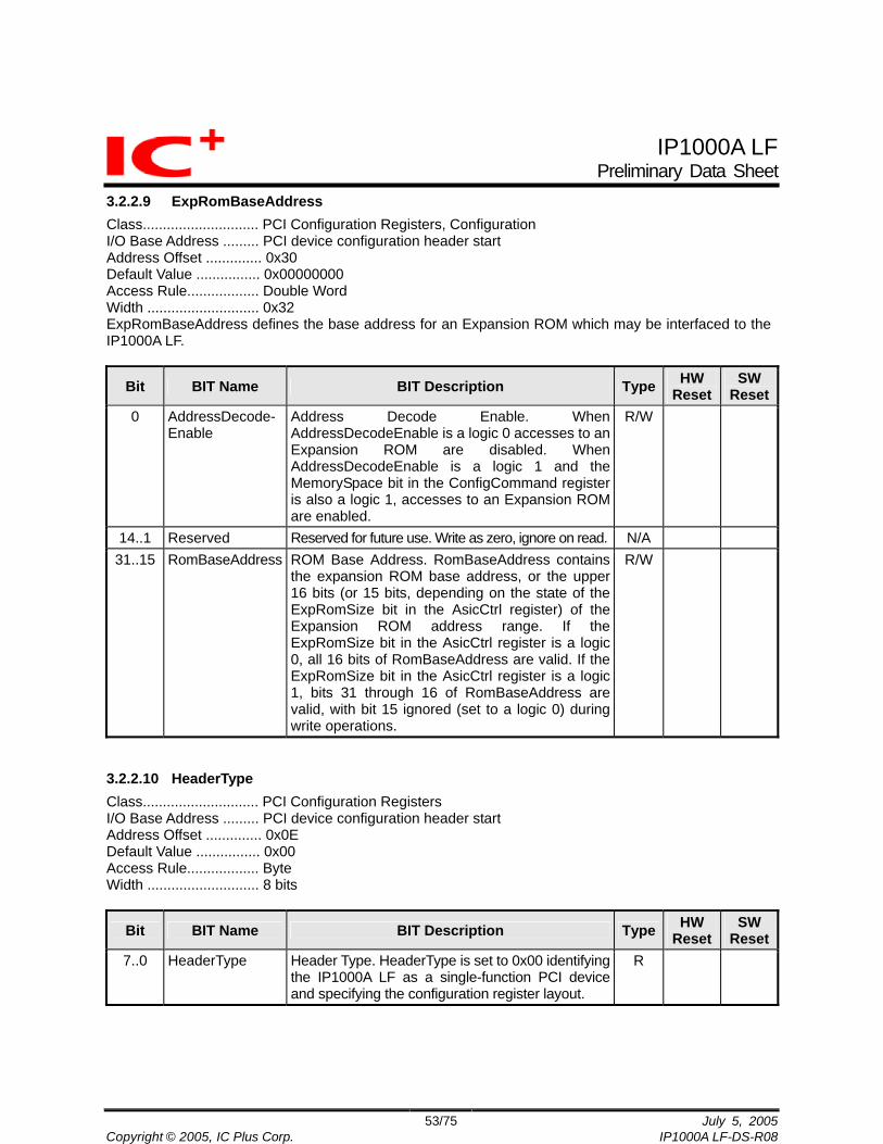
IP1000A LF Preliminary Data Sheet
53/75 July 5, 2005Copyright © 2005, IC Plus Corp. IP1000A LF-DS-R08
3.2.2.9 ExpRomBaseAddress Class............................. PCI Configuration Registers, Configuration I/O Base Address ......... PCI device configuration header start Address Offset .............. 0x30 Default Value ................ 0x00000000 Access Rule.................. Double Word Width ............................ 0x32 ExpRomBaseAddress defines the base address for an Expansion ROM which may be interfaced to the IP1000A LF.
Bit BIT Name BIT Description Type HW Reset
SW Reset
0 AddressDecode-Enable
Address Decode Enable. When AddressDecodeEnable is a logic 0 accesses to an Expansion ROM are disabled. When AddressDecodeEnable is a logic 1 and the MemorySpace bit in the ConfigCommand register is also a logic 1, accesses to an Expansion ROM are enabled.
R/W
14..1 Reserved Reserved for future use. Write as zero, ignore on read. N/A 31..15
RomBaseAddress ROM Base Address. RomBaseAddress contains
the expansion ROM base address, or the upper 16 bits (or 15 bits, depending on the state of the ExpRomSize bit in the AsicCtrl register) of the Expansion ROM address range. If the ExpRomSize bit in the AsicCtrl register is a logic 0, all 16 bits of RomBaseAddress are valid. If the ExpRomSize bit in the AsicCtrl register is a logic 1, bits 31 through 16 of RomBaseAddress are valid, with bit 15 ignored (set to a logic 0) during write operations.
R/W
3.2.2.10 HeaderType Class............................. PCI Configuration Registers I/O Base Address ......... PCI device configuration header start Address Offset .............. 0x0E Default Value ................ 0x00 Access Rule.................. Byte Width ............................ 8 bits
Bit BIT Name BIT Description Type HW Reset
SW Reset
7..0 HeaderType Header Type. HeaderType is set to 0x00 identifying the IP1000A LF as a single-function PCI device and specifying the configuration register layout.
R
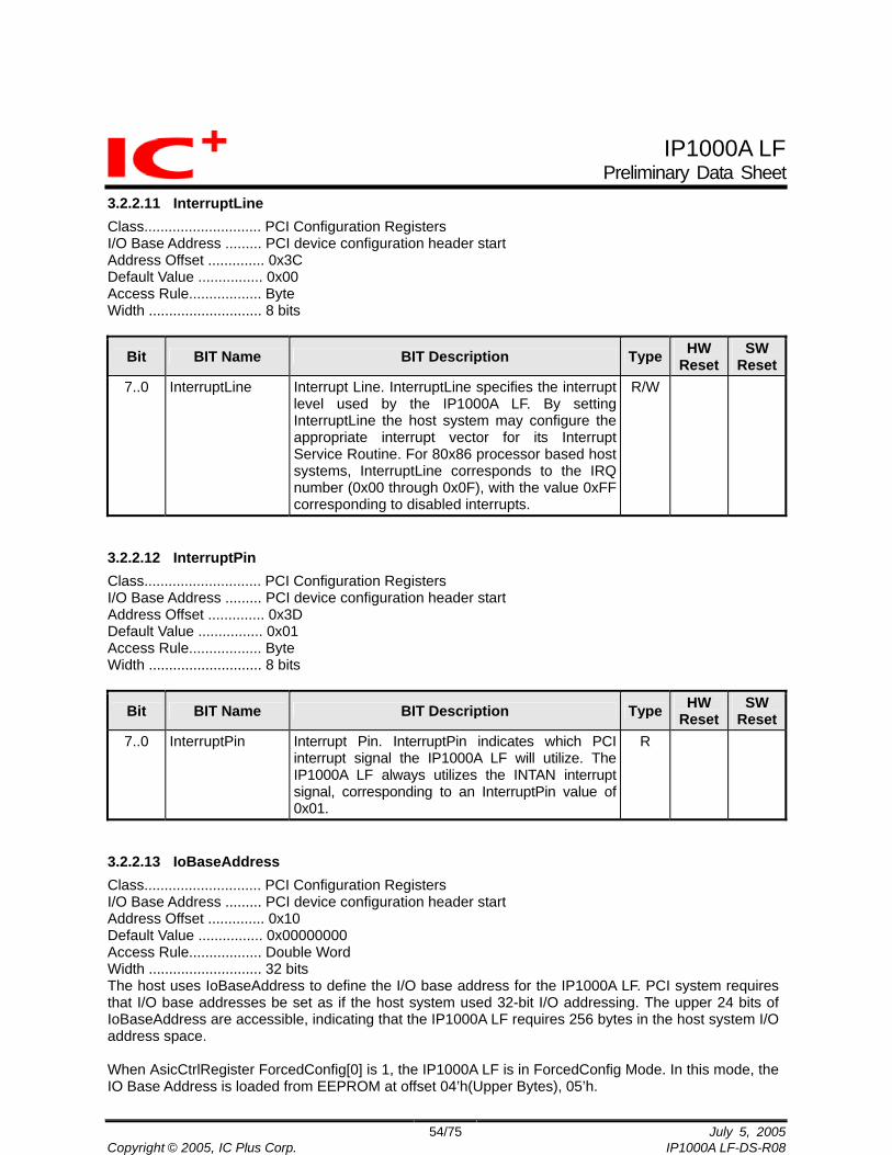
IP1000A LF Preliminary Data Sheet
54/75 July 5, 2005Copyright © 2005, IC Plus Corp. IP1000A LF-DS-R08
3.2.2.11 InterruptLine Class............................. PCI Configuration Registers I/O Base Address ......... PCI device configuration header start Address Offset .............. 0x3C Default Value ................ 0x00 Access Rule.................. Byte Width ............................ 8 bits
Bit BIT Name BIT Description Type HW Reset
SW Reset
7..0 InterruptLine Interrupt Line. InterruptLine specifies the interrupt level used by the IP1000A LF. By setting InterruptLine the host system may configure the appropriate interrupt vector for its Interrupt Service Routine. For 80x86 processor based host systems, InterruptLine corresponds to the IRQ number (0x00 through 0x0F), with the value 0xFF corresponding to disabled interrupts.
R/W
3.2.2.12 InterruptPin Class............................. PCI Configuration Registers I/O Base Address ......... PCI device configuration header start Address Offset .............. 0x3D Default Value ................ 0x01 Access Rule.................. Byte Width ............................ 8 bits
Bit BIT Name BIT Description Type HW Reset
SW Reset
7..0 InterruptPin Interrupt Pin. InterruptPin indicates which PCI interrupt signal the IP1000A LF will utilize. The IP1000A LF always utilizes the INTAN interruptsignal, corresponding to an InterruptPin value of 0x01.
R
3.2.2.13 IoBaseAddress Class............................. PCI Configuration Registers I/O Base Address ......... PCI device configuration header start Address Offset .............. 0x10 Default Value ................ 0x00000000 Access Rule.................. Double Word Width ............................ 32 bits The host uses IoBaseAddress to define the I/O base address for the IP1000A LF. PCI system requires that I/O base addresses be set as if the host system used 32-bit I/O addressing. The upper 24 bits of IoBaseAddress are accessible, indicating that the IP1000A LF requires 256 bytes in the host system I/O address space. When AsicCtrlRegister ForcedConfig[0] is 1, the IP1000A LF is in ForcedConfig Mode. In this mode, the IO Base Address is loaded from EEPROM at offset 04’h(Upper Bytes), 05’h.

IP1000A LF Preliminary Data Sheet
55/75 July 5, 2005Copyright © 2005, IC Plus Corp. IP1000A LF-DS-R08
Bit BIT Name BIT Description Type HW Reset
SW Reset
0 IoBaseAddrInd I/O Base Address Indicator. When IoBaseAddrInd is a logic 1, IoBaseAddress contains the valid I/O base address for the IP1000A LF.
R/W
7..1 Reserved Reserved for future use. Write as zero, ignore on read. N/A 31..8 IoBaseAddress I/O Base Address. IoBaseAddress contains the 24
bit I/O base address value. With 24 bits, the IP1000A LF uses 256 bytes of I/O address space.
R/W
3.2.2.14 LatencyTimer Class............................. PCI Configuration Registers I/O Base Address ......... PCI device configuration header start Address Offset .............. 0x0D Default Value ................ 0x00 Access Rule.................. Byte Width ............................ 8 bits
Bit BIT Name BIT Description Type HW Reset
SW Reset
2..0 Reserved Reserved for future use. Write as zero, ignore on read. N/A 7..3 LatencyTimer Latency Timer. LatencyTimer indicates, in
increments of 8 bus clocks, the length of time which the IP1000A LF may hold the PCI bus in the presence of other bus requestors. Whenever theIP1000A LF asserts the FRAMEN signal, the latency timer is started. When the latency timer count expires, the IP1000A LF must relinquish the bus as soon as its GNTN signal has been de-asserted.
R/W
3.2.2.15 MaxLat Class............................. PCI Configuration Registers, Configuration I/O Base Address ......... PCI device configuration header start Address Offset .............. 0x3F Default Value ................ 0x0A Access Rule.................. Byte Width ............................ 8 bits
Bit BIT Name BIT Description Type HW Reset
SW Reset
7..0 MaxLat Maximum Latency. MaxLat specifies, in 250 ns increments, how often the IP1000A LF requires bus access while operating as a bus master. Bits 5 through 1 of the MaxLat value are loaded from the ConfigParm field within an EEPROM during auto initialization of the IP1000A LF.
R

IP1000A LF Preliminary Data Sheet
56/75 July 5, 2005Copyright © 2005, IC Plus Corp. IP1000A LF-DS-R08
3.2.2.16 MemBaseAddress Class............................. PCI Configuration Registers I/O Base Address ......... PCI device configuration header start Address Offset .............. 0x14 Default Value ................ 0x00000000 Access Rule.................. Double Word Width ............................ 32 bits MemBaseAddress can be disabled via loading of the ConfigParm field from an EEPROM during auto-iniTialization of the IP1000A LF. When AsicCtrlRegister ForcedConfig[0] is 1, the IP1000A LF is in ForcedConfig Mode. In this mode, the MemBase Address is loaded from EEPROM at offset 04’h(Upper Bytes), 05’h, the same as IO BaseAddress.
Bit BIT Name BIT Description Type HW Reset
SW Reset
0 MemBaseAddrInd Memory Base Address Indicator. When MemBaseAddrInd is a logic 1, MemBaseAddress contains the valid memory base address.
R/W
2..1 MemMapType Memory Map Type. MemMapType defines how the host system maps the IP1000A LF’s registers within the host system memory space. Bit 2 of MemMapType is always a logic 0, while bit 1 isloaded from the Lower1Meg bit of the ConfigParm field within an EEPROM during auto initialization of the IP1000A LF.
BIT 2 BIT 1 REGISTER MAPPING 0 0 Anywhere within a 32 bit
address space 0 1 Lower 1 megabyte of 32 bit
address space 1 x Undefined
7..3 Reserved Reserved for future use. Write as zero, ignore on read. N/A 31..8 MemBaseAddress Memory Base Address. MemBaseAddress contains
the 24 bit memory base address value. With 24 bits, the IP1000A LF uses 256 bytes of I/O space.
R/W
3.2.2.17 MinGnt Class............................. PCI Configuration Registers I/O Base Address ......... PCI device configuration header start Address Offset .............. 0x3E Default Value ................ 0x50 Access Rule.................. Byte Width ............................ 8 bits
Bit BIT Name BIT Description Type HW Reset
SW Reset
7..0 MinGnt Minimum Grant Time. MinGnt specifies, in 250 ns increments, how long a burst period the IP1000A LF requires when operating as a bus master. Bits 7 through 4 of the MinGnt value are loaded from the ConfigParm field within an EEPROM during auto initialization of the IP1000A LF.
R

IP1000A LF Preliminary Data Sheet
57/75 July 5, 2005Copyright © 2005, IC Plus Corp. IP1000A LF-DS-R08
3.2.2.18 NextItemPtr0 Class............................. PCI Configuration Registers I/O Base Address ......... PCI device configuration header start Address Offset .............. 0x51 Default Value ................ 0x60 Access Rule.................. Byte Width ............................ 8 bits
Bit BIT Name BIT Description Type HW Reset
SW Reset
7..0 NextItemPtr Next Item Pointer. NextItemPtr indicates the next capability data structure in the capabilities list. When NextItemPtr is set to the value 0x00, there are no further data structures.
R
3.2.2.19 NextItemPtr1 Class............................. PCI Configuration Registers I/O Base Address ......... PCI device configuration header start Address Offset .............. 0x61 Default Value ................ 0x00 Access Rule.................. Byte Width ............................ 8 bits
Bit BIT Name BIT Description Type HW Reset
SW Reset
7..0 NextItemPtr Next Item Pointer. NextItemPtr indicates the next capability data structure in the capabilities list. When NextItemPtr is set to the value 0x00, there are no further data structures.
R
3.2.2.20 PowerMgmtCap Class............................. PCI Configuration Registers I/O Base Address ......... PCI device configuration header start Address Offset .............. 0x52 Default Value ................ 0x7602 Access Rule.................. Word Width ............................ 16 bits
Bit BIT Name BIT Description Type HW Reset
SW Reset
2..0 Version Version. Version is set to 0x2, indicating PCI Bus Power Management Specification Revision 1.1.
R
8..3 Reserved Reserved for future use. Write as zero, ignore on read. N/A 9 D1Support D1 Power State Support. When D1Support is a
logic 1, the IP1000A LF supports the D1 power state (see section 2.2.5.1). D1Support is loaded from the ConfigParm field of an EEPROM during auto initialization of the IP1000A LF.
R
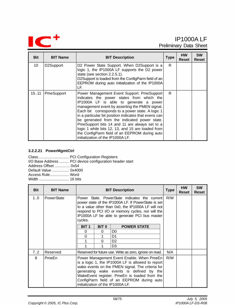
IP1000A LF Preliminary Data Sheet
58/75 July 5, 2005Copyright © 2005, IC Plus Corp. IP1000A LF-DS-R08
Bit BIT Name BIT Description Type HW Reset
SW Reset
10 D2Support D2 Power State Support. When D2Support is a logic 1, the IP1000A LF supports the D2 power state (see section 2.2.5.1). D2Support is loaded from the ConfigParm field of an EEPROM during auto initialization of the IP1000A LF.
R
15..11 PmeSupport Power Management Event Support. PmeSupport indicates the power states from which the IP1000A LF is able to generate a powermanagement event by asserting the PMEN signal. Each bit corresponds to a power state. A logic 1 in a particular bit position indicates that evens can be generated from the indicated power state.PmeSupport bits 14 and 11 are always set to a logic 1 while bits 12, 13, and 15 are loaded from the ConfigParm field of an EEPROM during auto initialization of the IP1000A LF.
R
3.2.2.21 PowerMgmtCtrl Class............................. PCI Configuration Registers I/O Base Address ......... PCI device configuration header start Address Offset .............. 0x54 Default Value ................ 0x4000 Access Rule.................. Word Width ............................ 16 bits
Bit BIT Name BIT Description Type HW Reset
SW Reset
1..0 PowerState Power State. PowerState indicates the current power state of the IP1000A LF. If PowerState is set to a value other than 0x0, the IP1000A LF will not respond to PCI I/O or memory cycles, nor will theIP1000A LF be able to generate PCI bus master cycles.
BIT 1 BIT 0 POWER STATE 0 0 D0 0 1 D1 1 0 D2 1 1 D3
R/W
7..2 Reserved Reserved for future use. Write as zero, ignore on read. N/A 8 PmeEn Power Management Event Enable. When PmeEn
is a logic 1, the IP1000A LF is allowed to report wake events on the PMEN signal. The criteria for generating wake events is defined by theWakeEvent register. PmeEn is loaded from the ConfigParm field of an EEPROM during auto initialization of the IP1000A LF.
R/W

IP1000A LF Preliminary Data Sheet
59/75 July 5, 2005Copyright © 2005, IC Plus Corp. IP1000A LF-DS-R08
Bit BIT Name BIT Description Type HW Reset
SW Reset
12..9 Data_Select Data Select is used to select which data is to be reported through the Data register and Data_Scale field.
R/W
14..13 Data_Scale Data Scale Only indicates the scaling factor to be used when interpreting the value of the Data register. The interpretation of the scale values is defined as follows:
DATA_SCALE SCALE FACTOR 0x0 Unknown 0x1 0.1 0x2 0.01 0x3 0.001
R
15 PmeStatus Power Management Event Status. When PmeStatus is a logic 1 a wake event has occurred. PmeStatus may be a logic 1 regardless of the value of PmeEn. Writing a logic 1 to PmeStatuswill set PmeStatus to a logic 0. Writing a logic 0 to PmeStatus has no effect.
R/W
3.2.2.22 RevisionId Class............................. PCI Configuration Registers I/O Base Address ......... PCI device configuration header start Address Offset .............. 0x08 Default Value ................ Depends on revision of actual device. See description below. Access Rule.................. Byte Width ............................ 8 bits
Bit BIT Name BIT Description Type HW Reset
SW Reset
7..0 RevisionId Revision ID= 41. RevisionId contains a revision code for the IP1000A LF.
R
3.2.2.23 SubsystemId Class............................. PCI Configuration Registers I/O Base Address ......... PCI device configuration header start Address Offset .............. 0x2E Default Value ................ 0x0000 Access Rule.................. Byte Width ............................ 16 bits
Bit BIT Name BIT Description Type HW Reset
SW Reset
15..0 SubsystemId Subsystem ID. SubsystemId contains the value loaded from the ConfigParm field within an EEPROM during auto initialization of the IP1000A LF.
R

IP1000A LF Preliminary Data Sheet
60/75 July 5, 2005Copyright © 2005, IC Plus Corp. IP1000A LF-DS-R08
SubsystemVendorId Class............................. PCI Configuration Registers I/O Base Address ......... PCI device configuration header start Address Offset .............. 0x2C Default Value ................ 0x0000 Access Rule.................. Word Width ............................ 16 bits
Bit BIT Name BIT Description Type HW Reset
SW Reset
15..0 SubsystemVendorId Subsystem Vendor ID. SubsystemVendorId contains the value loaded from the ConfigParm field within an EEPROM during auto initialization of the IP1000A LF.
R
3.2.2.24 VendorId Class............................. PCI Configuration Registers I/O Base Address ......... PCI device configuration header start Address Offset .............. 0x00 Default Value ................ 0x13F0 Access Rule.................. Word Width ............................ 16 bits
Bit BIT Name BIT Description Type HW Reset
SW Reset
15..0 VendorId Vendor ID. VendorId contains the unique 16-bit manufacturer’s ID as indicated by the PCI Special Interest Group. The manufacturer ID is 0x13F0.
R

IP1000A LF Preliminary Data Sheet
61/75 July 5, 2005Copyright © 2005, IC Plus Corp. IP1000A LF-DS-R08
3.2.3 EEPROM Fields Table 3-4 summarizes the layout of the data stored in an EEPROM connected to the IP1000A LF. Most defined EEPROM fields are read from the EEPROM and loaded into unique register bit positions within the IP1000A LF during auto initialization. In Table 3-4, all locations marked “Unused” and all locations not shown are not utilized by the IP1000A LF.
Table 3-4 : IP1000A LF EEPROM Field Layout
16 BIT WORD ADDR OFFSET StationAddress 12 StationAddress 11 StationAddress 10
Unused F Unused E Unused D Unused C Unused B Unused A Unused 9 Unused 8 Unused 7
LEDMode 6 PCI Register I/O, Mem Base[31:16] 5
PCI Register I/O, I/O, Mem Base[15:8] 4 SubsystemId 3
SubsystemVendorId 2 AsicCtrl 1
ConfigParm 0 3.2.3.1 ConfigParm Class............................. EEPROM Fields I/O Base Address ......... 0x00, accessed via the EepromCtrl register Address Offset .............. 0x00 Access Rule.................. Word Width ............................ 16 bits
Bit BIT Name BIT Description 0 FastBackToBack Fast Back to Back. FastBackToBack corresponds to the
FastBackTo-Back bit of the ConfigStatus register. 1 Lower1Meg Lower 1 Megabyte. Lower1Meg corresponds to bit 1 of the MemMap-Type
field in the MemBaseAddress register.
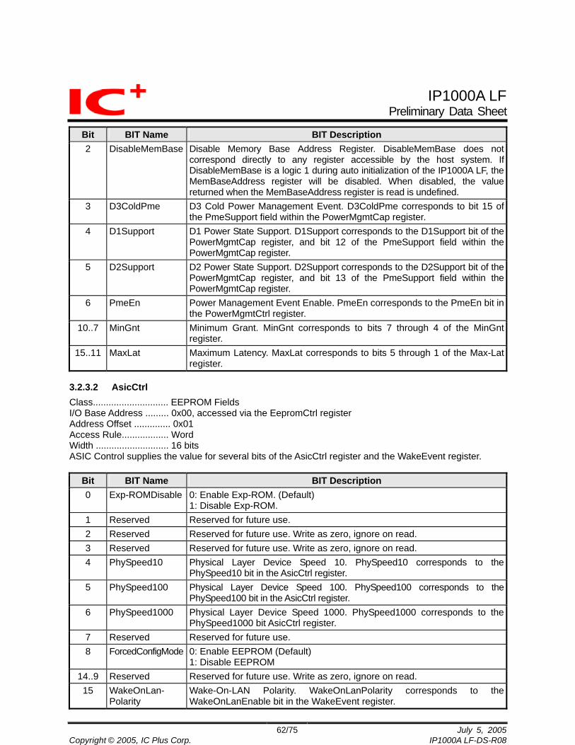
IP1000A LF Preliminary Data Sheet
62/75 July 5, 2005Copyright © 2005, IC Plus Corp. IP1000A LF-DS-R08
Bit BIT Name BIT Description 2 DisableMemBase Disable Memory Base Address Register. DisableMemBase does not
correspond directly to any register accessible by the host system. IfDisableMemBase is a logic 1 during auto initialization of the IP1000A LF, theMemBaseAddress register will be disabled. When disabled, the valuereturned when the MemBaseAddress register is read is undefined.
3 D3ColdPme D3 Cold Power Management Event. D3ColdPme corresponds to bit 15 of the PmeSupport field within the PowerMgmtCap register.
4 D1Support D1 Power State Support. D1Support corresponds to the D1Support bit of the PowerMgmtCap register, and bit 12 of the PmeSupport field within the PowerMgmtCap register.
5 D2Support D2 Power State Support. D2Support corresponds to the D2Support bit of the PowerMgmtCap register, and bit 13 of the PmeSupport field within the PowerMgmtCap register.
6 PmeEn Power Management Event Enable. PmeEn corresponds to the PmeEn bit in the PowerMgmtCtrl register.
10..7 MinGnt Minimum Grant. MinGnt corresponds to bits 7 through 4 of the MinGntregister.
15..11 MaxLat Maximum Latency. MaxLat corresponds to bits 5 through 1 of the Max-Latregister.
3.2.3.2 AsicCtrl Class............................. EEPROM Fields I/O Base Address ......... 0x00, accessed via the EepromCtrl register Address Offset .............. 0x01 Access Rule.................. Word Width ............................ 16 bits ASIC Control supplies the value for several bits of the AsicCtrl register and the WakeEvent register.
Bit BIT Name BIT Description 0 Exp-ROMDisable 0: Enable Exp-ROM. (Default)
1: Disable Exp-ROM. 1 Reserved Reserved for future use. 2 Reserved Reserved for future use. Write as zero, ignore on read. 3 Reserved Reserved for future use. Write as zero, ignore on read. 4 PhySpeed10 Physical Layer Device Speed 10. PhySpeed10 corresponds to the
PhySpeed10 bit in the AsicCtrl register. 5 PhySpeed100 Physical Layer Device Speed 100. PhySpeed100 corresponds to the
PhySpeed100 bit in the AsicCtrl register. 6 PhySpeed1000 Physical Layer Device Speed 1000. PhySpeed1000 corresponds to the
PhySpeed1000 bit AsicCtrl register. 7 Reserved Reserved for future use. 8 ForcedConfigMode 0: Enable EEPROM (Default)
1: Disable EEPROM 14..9 Reserved Reserved for future use. Write as zero, ignore on read. 15 WakeOnLan-
Polarity Wake-On-LAN Polarity. WakeOnLanPolarity corresponds to the WakeOnLanEnable bit in the WakeEvent register.

IP1000A LF Preliminary Data Sheet
63/75 July 5, 2005Copyright © 2005, IC Plus Corp. IP1000A LF-DS-R08
3.2.3.3 SubsystemVendorId Class............................. EEPROM Fields I/O Base Address ......... 0x00, accessed via the EepromCtrl register Address Offset .............. 0x02 Access Rule.................. Word Width ............................ 16 bits
Bit BIT Name BIT Description 15..0 SubsystemVendorId Subsystem Vendor ID. SubsystemVendorId corresponds to the
SubsystemVendorId register. 3.2.3.4 SubsystemId Class............................. EEPROM Fields I/O Base Address ......... 0x00, accessed via the EepromCtrl register Address Offset .............. 0x03 Access Rule.................. Word Width ............................ 16 bits
Bit BIT Name BIT Description 15..0 SubsystemId Subsystem ID. SubsystemId corresponds to the SubsystemId register.
3.2.3.5 PCI IO/Mem Base Address [15:8] Class............................. EEPROM Fields I/O Base Address ......... 0x00, accessed via the EepromCtrl register Address Offset .............. 0x04 Access Rule.................. Word Width ............................ 16 bits
Bit BIT Name BIT Description 0 APS Default setting as 1
7..1 Reserved Reserved for future use. 15..8 PCI IO/Mem Base
Address[15:8] At ForcedConfig Mode, PCI IO/Mem Base Address[15:8] are setted from the field.
3.2.3.6 PCI IO/Mem Base Address [31:16] Class............................. EEPROM Fields I/O Base Address ......... 0x00, accessed via the EepromCtrl register Address Offset .............. 0x05 Access Rule.................. Word Width ............................ 16 bits
Bit BIT Name BIT Description 15..0 PCI IO/Mem Base
Address[31:16] At ForcedConfig Mode, PCI IO/Mem Base Address[31:16] are setted from the field.

IP1000A LF Preliminary Data Sheet
64/75 July 5, 2005Copyright © 2005, IC Plus Corp. IP1000A LF-DS-R08
3.2.3.7 LEDMode Class............................. EEPROM Fields I/O Base Address ......... 0x00, accessed via the EepromCtrl register Address Offset .............. 0x06 Access Rule.................. Word Width ............................ 16 bits
Bit BIT Name BIT Description 1:0 LED Mode
BIT 1 BIT 0 LED MODE 0 0 LED MODE 0 0 1 LED MODE 1 (default) 1 0 LED MODE 2 1 1 LED MODE 3
LEDMode is used to control the LED signal pin (LEDLNK10N, LEDLNK100N, LEDLNK1000N, LEDDPLXN, LEDPWRN) functionality.
Pin LEDMode=1(default) LED10N Light_on= 10 link up
Light_off= 10 link down LED100N Light_on = 100 link up
Light_off = 100 link down LED1000N Light_on = 1000 link up
Light_off = 1000 link down LEDDPLXN Light_on = Full duplex
Light_off= Half duplex Blink = Collision
LEDRXN Light_off= not receiving Light_on = receiving
LEDTXN Light_off= not transmitting Light_on = transmitting Blink(00) = activity
Pin LEDMode=0 LED10N, LED100N
LED100,LED10= on,on = speed1000 on,off = speed100 off,on = speed10 off,off= link down
LED1000N Light_on = link up (any speed) Light_off=link down(any speed)
LEDDPLXN Light_on = Full duplex Light_off= Half duplex
LEDRXN Light_on= link up Light_off= link down Blink = receiving
LEDTXN Light_on= link up Light_off= link down Blink = activity
Pin LEDMode=2 LED10N Light_off= 10 link up
Blink slow = 100 link up Light_on= 1000 link up
LED100N Light on = 100 link up
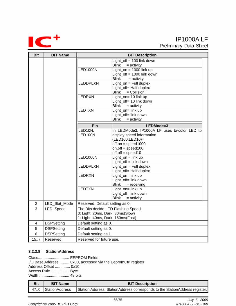
IP1000A LF Preliminary Data Sheet
65/75 July 5, 2005Copyright © 2005, IC Plus Corp. IP1000A LF-DS-R08
Bit BIT Name BIT Description Light_off = 100 link down Blink = activity
LED1000N Light_on = 1000 link up Light_off = 1000 link down Blink = activity
LEDDPLXN Light_on = Full duplex Light_off= Half duplex Blink = Collision
LEDRXN Light_on= 10 link up Light_off= 10 link down Blink = activity
LEDTXN Light_on= link up Light_off= link down Blink = activity
Pin LEDMode=3 LED10N, LED100N
In LEDMode3, IP1000A LF uses bi-color LED to display speed information. LED100,LED10= off,on = speed1000 on,off = speed100 off,off = speed10
LED1000N Light_on = link up Light_off = link down
LEDDPLXN Light_on = Full duplex Light_off= Half duplex
LEDRXN Light_on= link up Light_off= link down Blink = receiving
LEDTXN Light_on= link up Light_off= link down Blink = activity
2 LED_Stat_Mode Reserved. Default setting as 0. 3 LED_Speed The Bits decide LED Flashing Speed
0: Light: 20ms, Dark: 80ms(Slow) 1: Light: 40ms, Dark: 160ms(Fast)
4 DSPSetting Default setting as 0. 5 DSPSetting Default setting as 0. 6 DSPSetting Default setting as 1.
15..7 Reserved Reserved for future use. 3.2.3.8 StationAddress Class............................. EEPROM Fields I/O Base Address ......... 0x00, accessed via the EepromCtrl register Address Offset .............. 0x10 Access Rule.................. Byte Width ............................ 48 bits
Bit BIT Name BIT Description 47..0 StationAddress Station Address. StationAddress corresponds to the StationAddress register.

IP1000A LF Preliminary Data Sheet
66/75 July 5, 2005Copyright © 2005, IC Plus Corp. IP1000A LF-DS-R08
4 Absolute Maximum Ratings
Storage Temperature...................-65ºC to +150ºC Ambient Temperature ....................-65ºC to +70ºC Supply Voltage................................-0.3V to +3.6V Environmental stresses above those listed in Absolute Maximum Ratings may cause permanent damage resulting in device failure. Functionality at or above the limits listed below is not guaranteed. Exposure to the environmental stress at the levels listed below for extended periods may adversely affect device reliability. 5 Operating Ranges
Commercial Devices Temperature (T A ) .............................. 0ºC to +70ºC Supply Voltages (V CCH ) ..................... +3.3V ±10% Supply Voltages (V CCL ) ....................... +1.8V ±5% Input voltages .................................5V tolerant I/O Operating ranges define the limits of guaranteed device functionality. 6 DC Characteristics
DC characteristics are defined over commercial operating ranges unless specified otherwise. Operating Conditions
Parameter Sym. Min. Typ. Max. Unit Conditions Supply Voltage VCC 1.73 1.8 1.89 V Supply Voltage VCC_O 3.135 3.3 3.465 V Power Consumption 2.05 W 1000M full, VCC=1.8V,
VCC_O=3.3V Power Consumption 0.64 W 100M full, VCC=1.8V,
VCC_O=3.3V Power Consumption 0.63 W 10M full, VCC=1.8V,
VCC_O=3.3V Power Consumption 0.92 W 10M idle, VCC=1.8V,
VCC_O=3.3V Power Consumption (without LED power consumption)
Cable length 120m CAT5 Link Partner IP1000A LF Link condition Digital 1.8V Analog 1.8V CT 3.3V Digital 3.3V Analog 3.3V Actual voltage 1.8V 1.8V 3.3V 3.3V 3.3V
Watt
1000Mb Master 1000Mb D0 static 0.445A 0.197A 0.18A 0.02A 0.07A 2.05W 1000Mb D0 dynamic 0.450A 0.197A 0.18A 0.03A 0.07A 2.06W

IP1000A LF Preliminary Data Sheet
67/75 July 5, 2005Copyright © 2005, IC Plus Corp. IP1000A LF-DS-R08
1000Mb Slave 1000Mb D0 static 0.445A 0.197A 0.18A 0.02A 0.07A 2.05W 1000Mb D0 dynamic 0.449A 0.197A 0.18A 0.03A 0.07A 2.06W 100Mb 100Mb D0 static 0.105A 0.048A 0.05A 0.03A 0.03A 0.64W 100Mb D0 dynamic 0.108A 0.048A 0.05A 0.03A 0.03A 0.64W 10Mb 10Mb D0 static 0.037A 0.000A 0.10A 0.03A 0.04A 0.63W 10Mb D0 dynamic 0.037A 0.000A 0.10A 0.03A 0.04A 0.63W No Link D0 0.100A 0.101A 0.10A 0.03A 0.04A 0.92W Input Clock
Parameter Sym. Min. Typ. Max. Unit Conditions Frequency 25 MHz Frequency Tolerance -50 +50 PPM
I/O Electrical Characteristics
Parameter Sym. Min. Typ. Max. Unit Conditions Input Low Voltage VIL 0.8 V Input High Voltage VIH 2.0 V Output Low Voltage VOL 0.4 V IOH=4mA, VCC_O_x=3.3V Output High Voltage VOH 2.4 V IOL=4mA, VCC_O_x=3.3V
Parameter Symbol
Parameter Description Test Conditions Min Typ Max Unit
VCCH 3.3V power supply voltage 3.0 3.6 V VCCL 1.8V power supply voltage 1.73 1.89 V TTL I/O VIH Input high voltage(PCI Input Buffer
5V signalling) 2 V
VIL Input low voltage 0.8 V IIN Input High leakage current VIN=2.7V 10 µA IIN Input Low leakage current VIN=0.5V -10 µA VOH Output high voltage IOH=-2mA 2.4 V VOH TTL Output high voltage IOH=-4mA 2.4 V VOL TTL Output low voltage IOL=4mA 0.4 V VOL PCI Output low voltage IOL=3mA 0.55 V IOTS Output tri-state leakage ±10 µA
TABLE 6-1 : DC Characteristics.

IP1000A LF Preliminary Data Sheet
68/75 July 5, 2005Copyright © 2005, IC Plus Corp. IP1000A LF-DS-R08
7 Switching Characteristics
Parameter Symbol Parameter Description Test Conditions Min Typ Max Unit
66 MHz PCI Interface Trc RSTN cycle 300 nsTrr Rising Edge or RSTN to chip
recovery 1 µs
Tcc PCICLK cycle 15 nsTch PCICLK high 6 nsTcl PCICLK low 6 nsTrv PCICLK rise to bused signal valid 2 6 nsTrvp PCICLK rise to REQN, GNTN valid 2 6 nsTrzo PCICLK rise to signal on 2 nsTroz PCICLK rise to signal off 14 nsTsu bused signal setup wrt PCICLK rise 3 nsTsup1 GNTN setup wrt PCICLK rise 5 nsTsup2 REQN setup wrt PCICLK rise 5 nsThd signal hold wrt PCICLK rise 0 nsTrstoff RSTN low to output signal float 40 ns33MHz PCI Interface Trc RSTN cycle 300 nsTrr Rising edge or RSTN to chip
recovery 1 µs
Tcc PCICLK cycle 30 nsTch PCICLK high 11 nsTcl PCICLK lwo 11 nsTrv PCICLK rise to bused signal valid 2 11 nsTrvp PCICLK rise to REQN, GNTN valid 2 12 nsTrzo PCICLK rise to signal on 2 nsTroz PCICLK rise to signal off 28 nsTsu Bused signal setup wrt PCICLK rise 7 nsTsup1 GNTN setup wrt PCICLK rise 10 nsTsup2 REQN setup wrt PCICLK rise 12 nsThd Signal hold wrt PCICLK rise 0 nsTrstoff RSTN low to output signal float 40 nsExpansion Rom fC Clock Frequency for the following
instructions: FAST_READ, PP, SE, BE, DP, RES, WREN, WRDI, RDSR, WRSR
D.C. 25 MHz
fR Clock Frequency for READ instructions D.C. 20 MHztCH
1 Clock High Time 18 ns

IP1000A LF Preliminary Data Sheet
69/75 July 5, 2005Copyright © 2005, IC Plus Corp. IP1000A LF-DS-R08
Parameter Symbol Parameter Description Test Conditions Min Typ Max Unit
tCL1 Clock Low Time 18 ns
Clock Slew Rate2 (peak to peak) 0.1 V/nstSLCH S Active Setup Time (relative to C) 10 nstCHSL S Not Active Hold Time (relative to C) 10 nstDVCH Data In Setup Time 5 nstCHDX Data In Hold Time 5 nstCHSH S Active Hold Time (relative to C) 10 nstSHCH S Not Active Setup Time (relative to C) 10 nstSHSL S Deselect Time 100 nstSHQZ
2 Output Disable Time 15 nstCLQV Clock Low to Output Valid 15 nstCLQX Output Hold Time 0 nstHLCH HOLD Setup Time (relative to C) 10 nstCHHH HOLD Hold Time (relative to C) 10 nstHHCH HOLD Setup Time (relative to C) 10 nstCHHL HOLD Hold Time (relative to C) 10 nstHHQX
2 HOLD to Output Low-Z 15 nstHLQZ
2 HOLD to Output High-Z 20 nstDP
2 S High to Deep Power-down Mode 3 µstRES1
2 S High to Standby Mode without Electronic Signature Read
3 µs
tRES22 S High to Standby Mode with
Electronic Signature Read 1.8 µs
tW Write Status Register Cycle Time 5 15 mstPP Page Program Cycle Time 2 5 mstSE Sector Erase Cycle Time 2 3 s tBE Bulk Erase Cycle Time 3 6 s EEPROM Interface Tskc EESK cycle 1µs - nsTskh EESK high 250 - nsTskl EESK low 250 - nsTcs EECS low 250 - nsTpd EEDI valid wrt EESK rise 100 - nsTcsk EECS setup wrt EESK rise 50 - nsTcsh EECS hold wrt EESK fall 0 - nsTdos EEDO setup wrt EESK rise 70 500 nsTdoh EEDO hold wrt EESK rise - 500 nsMII Interface (10/100) – Transmit Tcc TXCLK cycle T=1 when 100Mb/s;
10 when 10Mb/s 40T ns

IP1000A LF Preliminary Data Sheet
70/75 July 5, 2005Copyright © 2005, IC Plus Corp. IP1000A LF-DS-R08
Parameter Symbol Parameter Description Test Conditions Min Typ Max Unit
Tch TXCLK high 14T 26T nsTcl TXCLK low 14T 26T nsTrv TXCLK rise to TXD, TXEN valid 20 nsTrh TXD, TXEN hold after TXCLK rise 5 nsMII Interface (10/100) – Receive Tcc RXCLK cycle T=1 when 100Mb/s;
10 when 10Mb/s - 40T ns
Tch RXCLK high 14T 26T nsTcl RXCLK low 14T 26T nsTsu RXD, RXER, RXDV setup wrt
RXCLK rise 10 20 ns
Thd RXD, RXER, RXDV hold wrt RXCLK rise
5 ns
GMII Interface (1000) – Transmit Tcc GTXCLK cycle 8 nsTch GTXCLK high 7.5 8.5 nsTcl GTXCLK low 7.5 8.5 nsTrv GTXCLK rise to TXD, TXEN valid 20 nsTrh TXD, TXEN hold after GTXCLK rise 5 nsGMII Interface (1000) – Receive Tcc RXCLK0 cycle - 8 nsTch RXCLK0 high 7.5 8.5 nsTcl RXCLK0 low 7.5 8.5 nsTsu RXD, RXER, RXDV setup wrt
RXCLK0 rise 10 20 ns
Thd RXD, RXER, RXDV hold wrt RXCLK0 rise
5 ns
MII Interface – Management Tcc MDC cycle 400 - - nsTch MDC high 160 - nsTcl MDC low 160 - nsTsu MDIO setup wrt MDC rise 10 - nsThd MDIO hold wrt MDC rise 10 - nsTrv MDC rise to MDIO valid - 20 nsMISC Interface Tcc CLK125 cycle 8.0 nsTch CLK125 high 4.0 nsTcl CLK125 low 4.0 ns

IP1000A LF Preliminary Data Sheet
71/75 July 5, 2005Copyright © 2005, IC Plus Corp. IP1000A LF-DS-R08
TABLE 7.1 : Switching Characteristics.
RSTN
PCICLK
REQN
IP10
00A
LF
trv
BUSSED SIGNALS
GNTN
ANY SIGNAL
ANY SIGNAL
tsu
tcl
tsup2trvp
tsup1trvp
trzothd
troz trstoff
trc
tcc tch
FIGURE 7-1: PCI Switching Characteristics
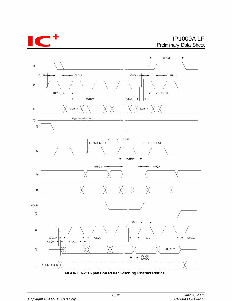
IP1000A LF Preliminary Data Sheet
72/75 July 5, 2005Copyright © 2005, IC Plus Corp. IP1000A LF-DS-R08
tSHSL
S
C
D
Q
tCHSL tSLCH
tDVCH
tCHDX
MSB IN LSB IN
tCLCH
tCHCL
tCHSH tSHCH
High Impedance
S
C
D
Q
tHLQZ tHHQX
tHHCH
HOLD
tCHHH
tHLCHtCHHL
S
C
Q
D
tCLQV tCL tSHQZ
tCH
ADDR.LSB IN
LSB OUT
tQLQHtQHQL
tCLQXtCLQXtCLQV
FIGURE 7-2: Expansion ROM Switching Characteristics.

IP1000A LF Preliminary Data Sheet
73/75 July 5, 2005Copyright © 2005, IC Plus Corp. IP1000A LF-DS-R08
EECS
EESK
EEDI
EEDO
IP10
00A
LF
tcshtcs
tcskvtskl tskc tskh
tpd
tdostdoh
A7 A0
D15 D0
FIGURE 7-3: EEPROM Switching Characteristics
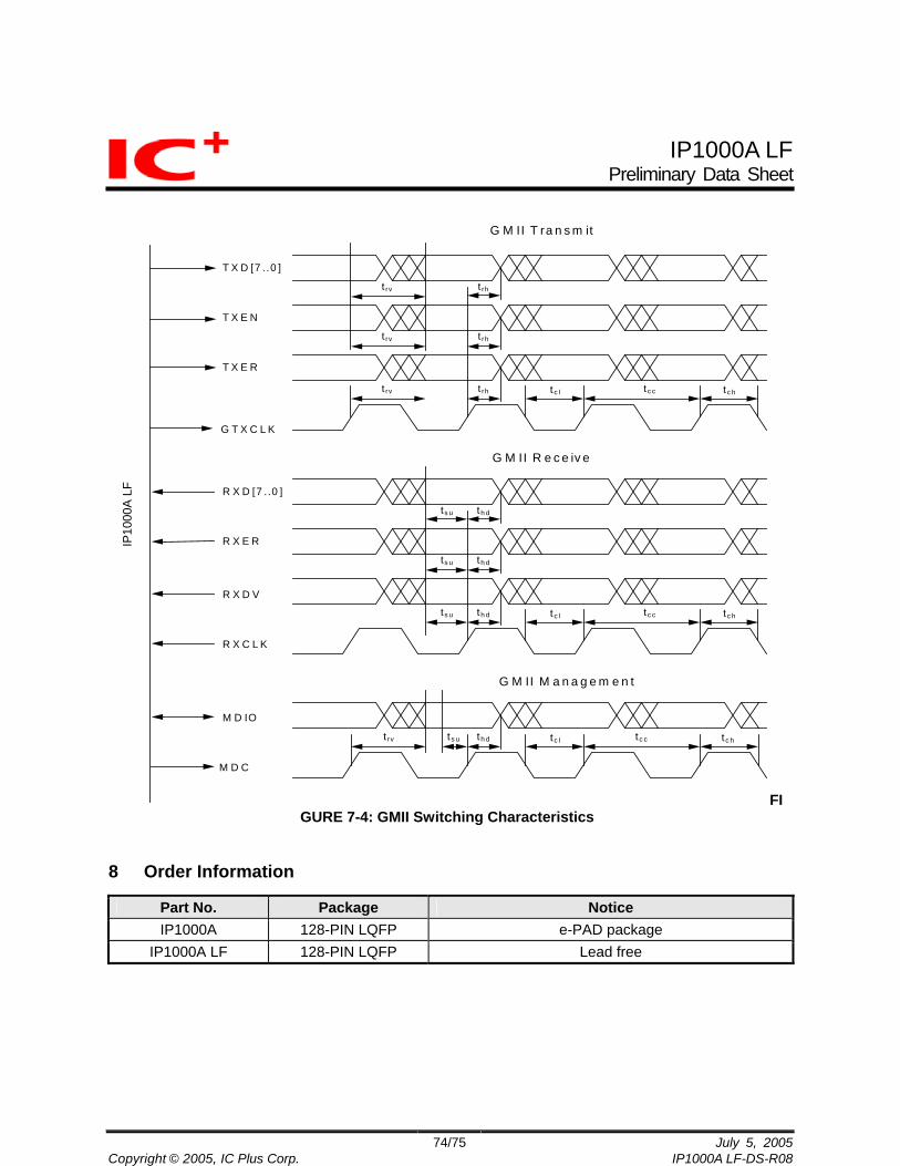
IP1000A LF Preliminary Data Sheet
74/75 July 5, 2005Copyright © 2005, IC Plus Corp. IP1000A LF-DS-R08
t rv t rh
t rv t rh
t rv t rh t c l t c c t c h
T X D [7 ..0 ]
T X E N
G T X C L K
IP10
00A
LF
T X E R
R X D [7 ..0 ]
R X E R
R X C L K
th d
th d
th d t c l t c c t c h
G M II T ra n s m it
G M II R e c e iv e
ts u
ts u
ts u
G M II M a n a g e m e n t
t rv t s u th d t c l t c c t c h
R X D V
M D IO
M D C
FIGURE 7-4: GMII Switching Characteristics
8 Order Information
Part No. Package Notice IP1000A 128-PIN LQFP e-PAD package
IP1000A LF 128-PIN LQFP Lead free

IP1000A LF Preliminary Data Sheet
9 Package Detail
LQFP 128 Outline Dimensions
IC Plus Corp. Headquarters Sales Office 10F, No.47, Lane 2, Kwang-Fu Road, Sec. 2, 4F, No. 106, Hsin-Tai-Wu Road, Sec.1, Hsin-Chu City, Taiwan 300, R.O.C. Hsi-Chih, Taipei Hsien, Taiwan 221, R.O.C. TEL : 886-3-575-0275 FAX : 886-3-575-0475 TEL : 886-2-2696-1669 FAX : 886-2-2696-2220Website: www.icplus.com.tw
75/75 July 5, 2005Copyright © 2005, IC Plus Corp. IP1000A LF-DS-R08
Related Documents


![[PPT]PowerPoint 프레젠테이션cfs3.tistory.com/upload_control/download.blog?fhandle=... · Web view... 1 VLAN 2 Backbone VLAN 1 VLAN 1 VLAN 2 VLAN 1 VLAN 2 VLAN 1 VLAN 2 물리적인](https://static.cupdf.com/doc/110x72/5ac031517f8b9a213f8bb25a/pptpowerpoint-cfs3-view-1-vlan-2-backbone-vlan-1-vlan-1.jpg)